registers, counters, and clock - school of...
TRANSCRIPT

Registers, Counters, and Clock
Z. Jerry ShiComputer Science and Engineering
University of Connecticut
Thank John Wakerly for providing his slides and figures.

Multibit registers
• 74x175 (4 bits)
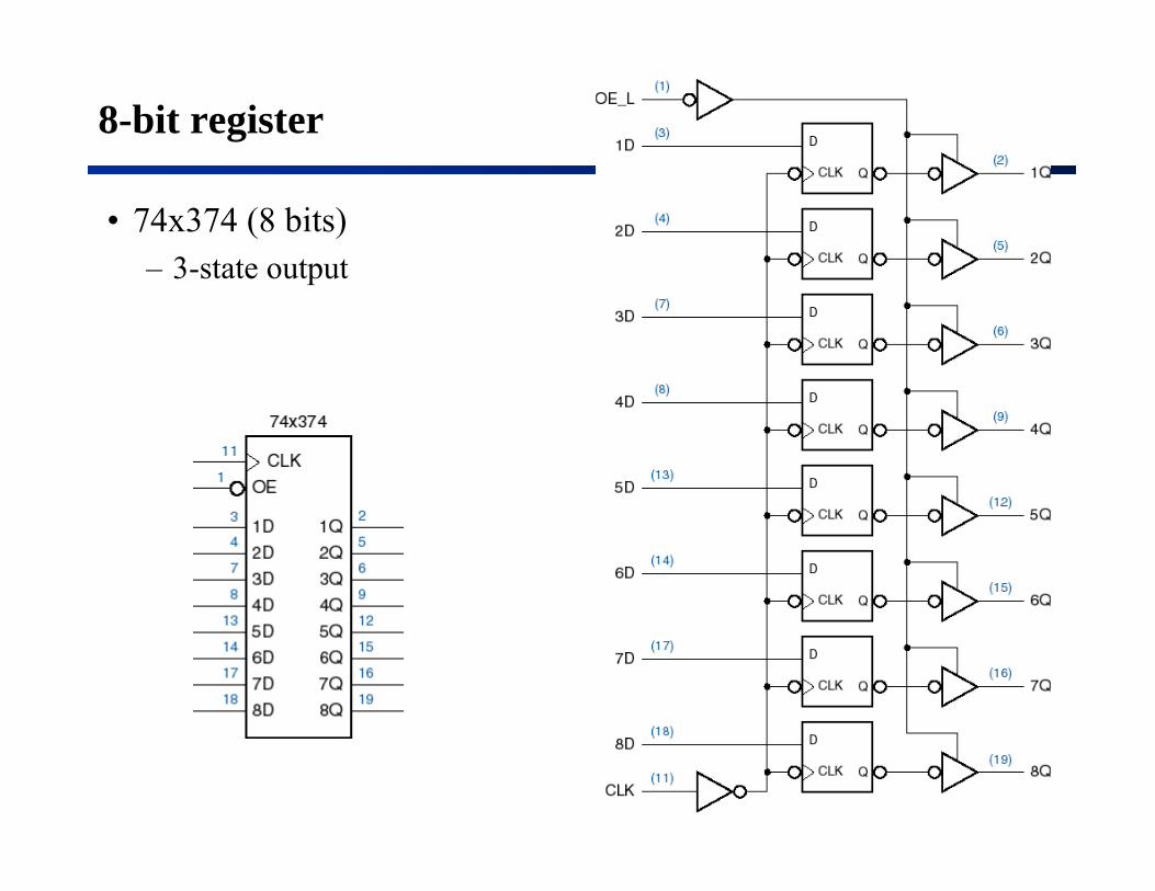
8-bit register
• 74x374 (8 bits)– 3-state output

Other octal registers
• 74x273– Asynchronous clear
• 74x377– Enable

Octal latch
• 74x373– Output enable– Latch-enable input “C” or “G”
• Register vs. latch, what’s the difference?– Register: edge-triggered behavior– Latch: output follows input when G is asserted

Counters
• Any sequential circuit whose state diagram is a single cycle.
RESET EN
EN
ENEN EN
EN
EN
EN′EN′ EN′
EN′EN′EN′

Ripple counter
• Q0 changes at the rising edge of CLK• Q1 changes when Q0: 1 0• Q2 changes when A1: 1 0
000000010010001101000101011001111000….
Long delay
LSB
MSB
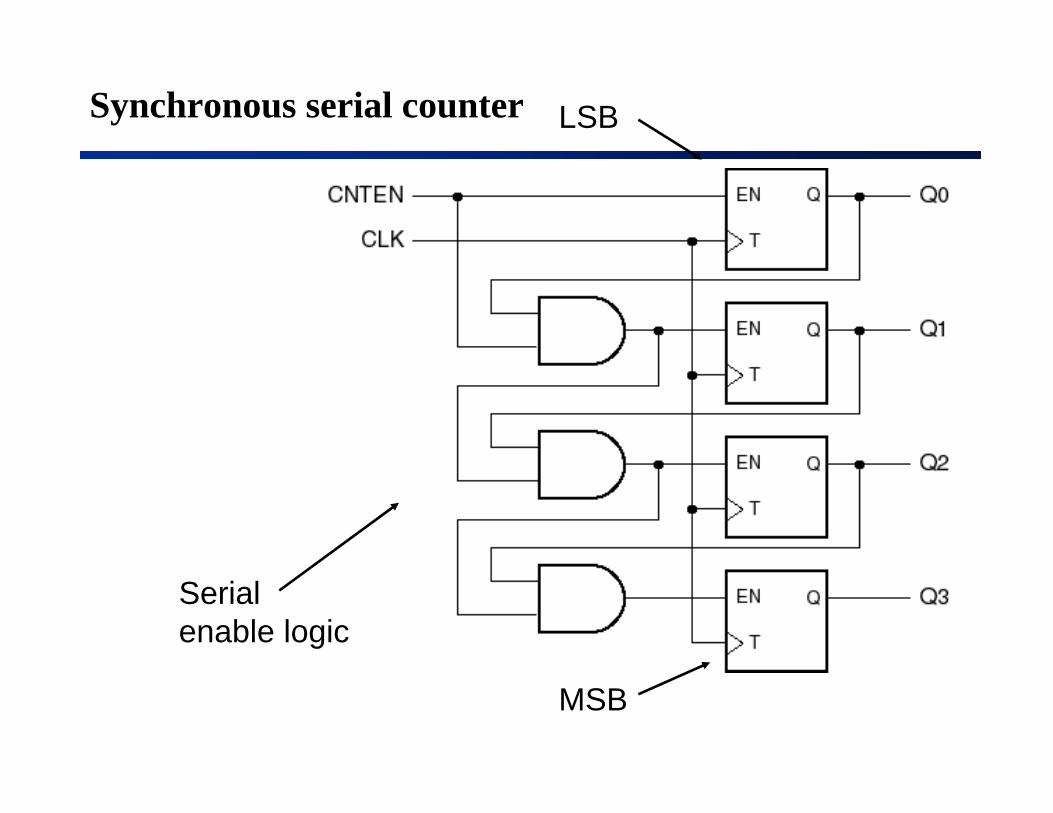
Synchronous serial counter
Serial enable logic

LSB
MSB
Synchronous parallel counter
Parallel enable logic

74x163 MSI 4-bit counter

74x163 internal logic diagram
• XOR gates embody the “T” function
• Mux-like structure for loading
S0 = CLR_L • LDS1 = CLR_L • S0′CLR_L = 0:
00: Clear CLR_L = 1:
01: Load10: Counter
RCO = QA•QB•QC•QD•ENT(may change in a cycle)
S0
S1

Counter operation
• Free-running ÷16• Count if ENP and
ENT both asserted.• Load if LD is asserted
(overrides counting).• Clear if CLR is asserted (overrides loading and counting).• All operations take place on rising CLK edge.• RCO is asserted if ENT is asserted and
Count = 15.

Free-running 4-bit ’163 counter
• “divide-by-16” counter

Modified counting sequence
• Load 0101 (5) after Count = 15• 5, 6, 7, 8, 9, 10, 11, 12, 13, 14, 15, 5, 6, …• “divide-by-11” counter

Another way
• Clear after Count = 1010 (10)• 0, 1, 2, 3, 4, 5, 6, 7, 8, 9, 10, 0, 1, 2, 3, …• “modulo-11” or “divide-by-11” counter
trick to save gate inputs

Counting from 3 to 12

Cascading counters
• RCO (ripple carry out) is asserted in state 15, if ENT is asserted.

Decoding binary-counter states

Decoder waveforms
• Glitches may or may not be a concern.– Control signals to R-S latch– Inputs to other flip flops

Glitch-free outputs
• Registered outputs delayed by one clock tick.• We’ll show another way to get the same outputs later, using a
shift register.

Up/down counter 74x169
• Similar to 74x163• Active low RCO, ENP, and ENT• Can go up and down
UP/DN=1: 0, 1, 2, 3, 4, …, 15, 0, 1, 2, …
UP/DN=0: 15, 14, 13, …, 2, 1, 0, 15, 14, …

74x169Logic diagram
2-1 MUX for loading
XOR’s implement T flip-flops
U controls a 2-1 MUX inverting the data signal
When U = 1, En = (QA′ + QB′ + QC′)′= QA • QB • QC
When U = 0,En = (( QA′ • QB′ • QC′)′)′= QA′ • QB′ • QC′

Shift registers
• For handling serial data– Such as RS-232, modem
transmission and reception, Ethernet links, etc.
• Serial-in, serial-out

Serial-to-parallel conversion
• Use a serial-in, parallel-out shift register
• The output of all D flip-flops are accessible
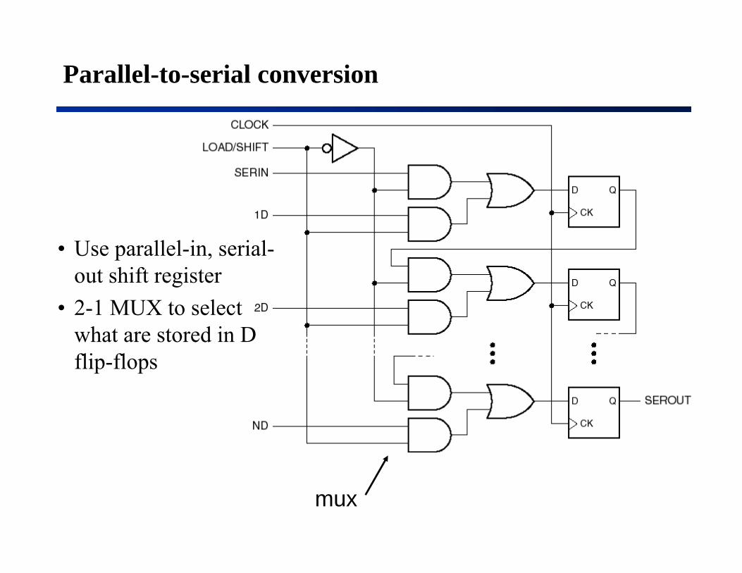
Parallel-to-serial conversion
• Use parallel-in, serial-out shift register
• 2-1 MUX to select what are stored in D flip-flops
mux

Do both
• Parallel-in, parallel-out shift register
• D flip-flops are accessible

“Universal” shift register 74x194
• Four functions– Shift left– Shift right– Load– Hold
• 4-1 MUXes to select correct input to D flip-flops
• Clear function
Control signals

One stage of 74x194

Ring counters
• Shift registers

State diagram of the simple ring counter

Self-correcting 4-bit, 4-state ring counter
Single circulating 1

State diagram for the self-correcting ring counter

Linear Feedback Shift Register (LFSR)
• 2n - 1 states before repeating• Pseudo-random number generator

Feedback equations for all values of n

Functional timing

Delays in state machines
Setup-time margin = t_clk – t_ffpd_max – t_comb_max – t_setup > 0Hold-time margin = t_ffpd_min + t_comb_min – t_hold > 0

Clock Skew
• Clock signal may not reach all flip-flops simultaneously• Output changes of flip-flops with “early” clock may reach D
inputs of flip-flops with “late” clock too soon
Reasons for slowness:(a) wiring delays(b) capacitance(c) incorrect design

Clock-skew calculation
tffpd(min) + tcomb(min) – thold > tskew(max)
tffpd(min) + tcomb(min) > tskew(max) + thold
• Clock skew should be smaller than the hold-time margin• Compensating for clock skew:
– Longer flip-flop propagation delay– Explicit combinational delays– Shorter (even negative) flip-flop hold times

Example of bad clock distribution

Clock distribution in ASICs
• This is what a typical ASIC router will do if you don’t lay out the clock by hand.

“Clock-tree” solution
• Often laid out by hand (H-tree)• Wide,fast metal (low R ==> fast RC time constant)

Gating the clock
• Definitely a no-no– Glitches possible if control signal (CLKEN) is generated by
the same clock– Excessive clock skew in any case.

If you really must gate the clock...

Control unit and data unit
• Divide large state machines into smaller machines• Data unit
– Data processing• Storing, moving, combing, etc.
– Registers, specialized functions (adder, shifter), memory• Control unit
– Starting, stopping actions in data units– Testing conditions– Deciding what to do next
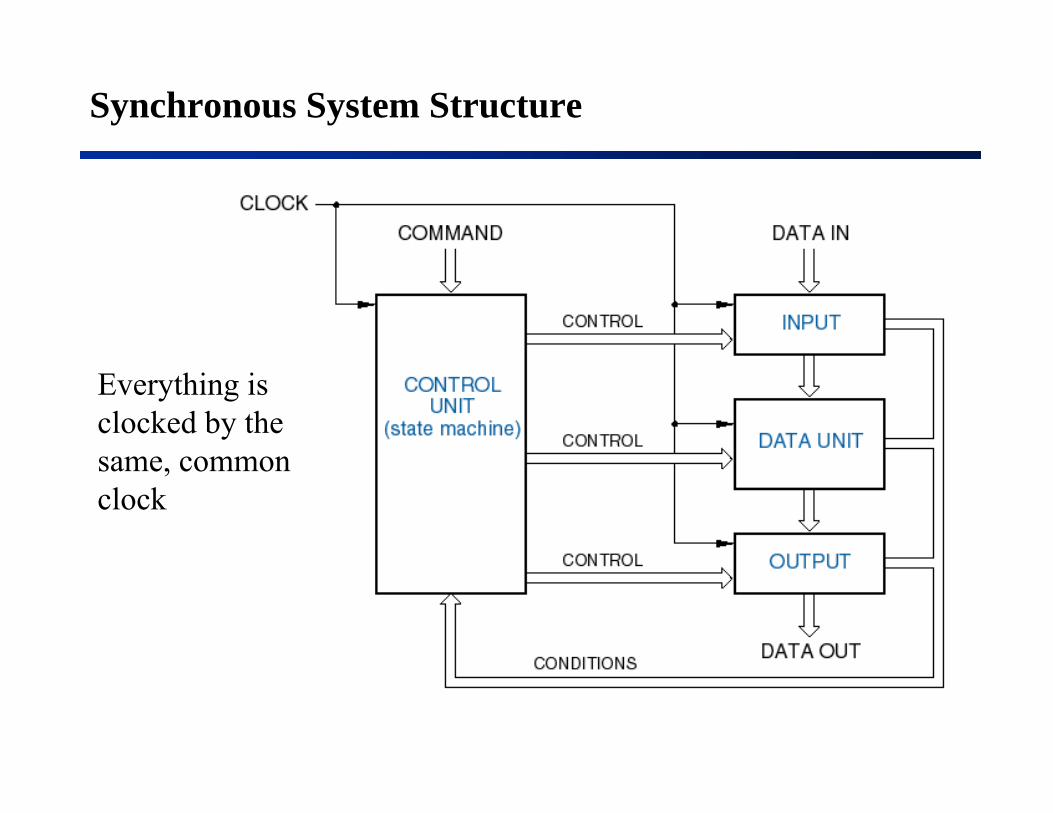
Synchronous System Structure
Everything is clocked by the same, common clock

Typical synchronous-system timing
• Outputs have one complete clock period to propagate to inputs.• Must take into account flip-flop setup times at next clock period.