flip flops, counters & registers
TRANSCRIPT

FLIP FLOPS, COUNTERS & REGISTERS

FLIP FLOPS

FLIP FLOPS Introduction Memory Elements Pulse-Triggered Latch
S-R LatchGated S-R LatchGated D Latch
Edge-Triggered Flip-flopsS-R Flip-flopD Flip-flopJ-K Flip-flopT Flip-flop
Asynchronous Inputs

4
INTRODUCTION
A sequential circuit consists of a feedback path, and employs some memory elements.
Combinational logic
Memory elements
Combinational outputs Memory outputs
External inputs
Sequential circuit = Combinational logic + Memory Elements

INTRODUCTION There are two types of sequential circuits:
synchronous: outputs change only at specific timeasynchronous: outputs change at any time
Multivibrator: a class of sequential circuits. They can be:bistable (2 stable states)monostable or one-shot (1 stable state)astable (no stable state)
Bistable logic devices: latches and flip-flops. Latches and flip-flops differ in the method
used for changing their state.

SEQUENTIAL CIRCUITS
CombinationalCircuit Memory
Elements
Inputs Outputs
• Asynchronous
• Synchronous
CombinationalCircuit
Flip-flops
Inputs Outputs
Clock

MEMORY ELEMENTS Memory element: a device which can
remember value indefinitely, or change value on command from its inputs.
Characteristic table:
Command(at time t)
Q(t) Q(t+1)
Set X 1
Reset X 0
0 0Memorise /No Change 1 1
command Memory element stored value
Q
Q(t): current stateQ(t+1) or Q+: next state

MEMORY ELEMENTS Memory element with clock. Flip-flops are
memory elements that change state on clock signals.
Clock is usually a square wave.
command Memory element stored value
Q
clock
Positive edges Negative edges
Positive pulses

MEMORY ELEMENTS Two types of triggering/activation:
pulse-triggerededge-triggered
Pulse-triggeredlatchesON = 1, OFF = 0
Edge-triggeredflip-flopspositive edge-triggered (ON = from 0 to 1; OFF =
other time)negative edge-triggered (ON = from 1 to 0; OFF =
other time)

11 / 60
LATCHES• SR Latch
R
S
Q
Q
S R Q0 Q Q’0 0 0
0
1
0
0
0 1 Q = Q0
Initial Value

12 / 60
LATCHES• SR Latch
R
S
Q
Q
S R Q0 Q Q’0 0 0 0 10 0 1
1
0
0
0
1 0 Q = Q0
Q = Q0

13 / 60
LATCHES• SR Latch
R
S
Q
Q
S R Q0 Q Q’0 0 0 0 10 0 1 1 00 1 0 0
0
1
1
0
1 Q = 0
Q = Q0

14 / 60
LATCHES• SR Latch
R
S
Q
Q
S R Q0 Q Q’0 0 0 0 10 0 1 1 00 1 0 0 10 1 11
0
1
0
0 1Q = 0
Q = Q0
Q = 0

15 / 60
LATCHES• SR Latch
R
S
Q
Q
S R Q0 Q Q’0 0 0 0 10 0 1 1 00 1 0 0 10 1 1 0 11 0 0
0
1
0
1
1 0
Q = 0
Q = Q0
Q = 1

16 / 60
LATCHES• SR Latch
R
S
Q
Q
S R Q0 Q Q’0 0 0 0 10 0 1 1 00 1 0 0 10 1 1 0 11 0 0 1 01 0 1
1
0
0
1
1 0
Q = 0
Q = Q0
Q = 1Q = 1

17 / 60
LATCHES• SR Latch
R
S
Q
Q
S R Q0 Q Q’0 0 0 0 10 0 1 1 00 1 0 0 10 1 1 0 11 0 0 1 01 0 1 1 01 1 0
0
1
1
1
0 0
Q = 0
Q = Q0
Q = 1
Q = Q’
0

18 / 60
LATCHES• SR Latch
R
S
Q
Q
S R Q0 Q Q’0 0 0 0 10 0 1 1 00 1 0 0 10 1 1 0 11 0 0 1 01 0 1 1 01 1 0 0 01 1 1
1
0
1
1
0 0
Q = 0
Q = Q0
Q = 1
Q = Q’
0
Q = Q’

19 / 60
LATCHES• SR Latch
R
S
Q
Q
S R Q0 0 Q0
0 1 01 0 11 1 Q=Q’=0
No changeResetSetInvalid
S
R
Q
Q
S R Q0 0 Q=Q’=10 1 11 0 01 1 Q0
InvalidSetResetNo change

20 / 60
LATCHES• SR Latch
R
S
Q
Q
S R Q0 0 Q0
0 1 01 0 11 1 Q=Q’=0
No changeResetSetInvalid
S’ R’ Q0 0 Q=Q’=10 1 11 0 01 1 Q0
InvalidSetResetNo change
S
R
Q
Q

21 / 60
CONTROLLED LATCHES• SR Latch with Control Input
C S R Q0 x x Q0
1 0 0 Q0
1 0 1 01 1 0 11 1 1 Q=Q’
No changeNo changeResetSetInvalid
S
R
Q
Q
S
R
C
S
RQ
QS
R
C

22 / 60
CONTROLLED LATCHES• D Latch (D = Data)
C D Q0 x Q0
1 0 01 1 1
No changeResetSet
S
R
Q
Q
D
C
C
Timing Diagram
D
Q
t
Output may change

23 / 60
CONTROLLED LATCHES• D Latch (D = Data)
C D Q0 x Q0
1 0 01 1 1
No changeResetSet
C
Timing Diagram
D
Q
Output may change
S
R
Q
Q
D
C

LATCH CIRCUITS: NOT SUITABLE Latch circuits are not suitable in synchronous
logic circuits. When the enable signal is active, the
excitation inputs are gated directly to the output Q. Thus, any change in the excitation input immediately causes a change in the latch output.
The problem is solved by using a special timing control signal called a clock to restrict the times at which the states of the memory elements may change.
This leads us to the edge-triggered memory elements called flip-flops.

25 / 60
FLIP-FLOPS• Controlled latches are level-triggered
• Flip-Flops are edge-triggered
C
CLK Positive Edge
CLK Negative Edge

26 / 60
FLIP-FLOPS• Master-Slave D Flip-Flop
D Latch (Master)
D
C
Q D Latch (Slave)
D
C
Q QD
CLKCLK
D
QMaster
QSlave
Looks like it is negative edge-triggered
Master Slave

27 / 60
FLIP-FLOPS• Edge-Triggered D Flip-Flop
D
CLKQ
Q
D Q
Q
D Q
Q
Positive Edge
Negative Edge

28 / 60
FLIP-FLOPS• JK Flip-Flop
D Q
Q
Q
QCLK
J
K
J Q
QK
D = JQ’ + K’Q

29 / 60
FLIP-FLOPS• T Flip-Flop
D = TQ’ + T’Q = T Q
J Q
QK
T D Q
Q
T
D = JQ’ + K’QT Q
Q

30 / 60
FLIP-FLOP CHARACTERISTIC TABLESD Q
Q
D Q(t+1)0 01 1
ResetSet
J K Q(t+1)0 0 Q(t)0 1 01 0 11 1 Q’(t)
No changeResetSetToggle
J Q
QK
T Q
Q
T Q(t+1)0 Q(t)1 Q’(t)
No changeToggle

31 / 60
FLIP-FLOP CHARACTERISTIC EQUATIONSD Q
Q
D Q(t+1)0 01 1
Q(t+1) = D
J K Q(t+1)0 0 Q(t)0 1 01 0 11 1 Q’(t)
Q(t+1) = JQ’ + K’QJ Q
QK
T Q
Q
T Q(t+1)0 Q(t)1 Q’(t)
Q(t+1) = T Q

32 / 60
FLIP-FLOP CHARACTERISTIC EQUATIONS• Analysis / Derivation
J Q
QK
J K Q(t) Q(t+1)0 0 0 00 0 1 10 1 00 1 11 0 01 0 11 1 01 1 1
No change
Reset
Set
Toggle

33 / 60
FLIP-FLOP CHARACTERISTIC EQUATIONS• Analysis / Derivation
J Q
QK
J K Q(t) Q(t+1)0 0 0 00 0 1 10 1 0 00 1 1 01 0 01 0 11 1 01 1 1
No change
Reset
Set
Toggle
34 / 60
FLIP-FLOP CHARACTERISTIC EQUATIONS• Analysis / Derivation
J Q
QK
J K Q(t) Q(t+1)0 0 0 00 0 1 10 1 0 00 1 1 01 0 0 11 0 1 11 1 01 1 1
No change
Reset
Set
Toggle

35 / 60
FLIP-FLOP CHARACTERISTIC EQUATIONS• Analysis / Derivation
J Q
QK
J K Q(t) Q(t+1)0 0 0 00 0 1 10 1 0 00 1 1 01 0 0 11 0 1 11 1 0 11 1 1 0
No change
Reset
Set
Toggle

36 / 60
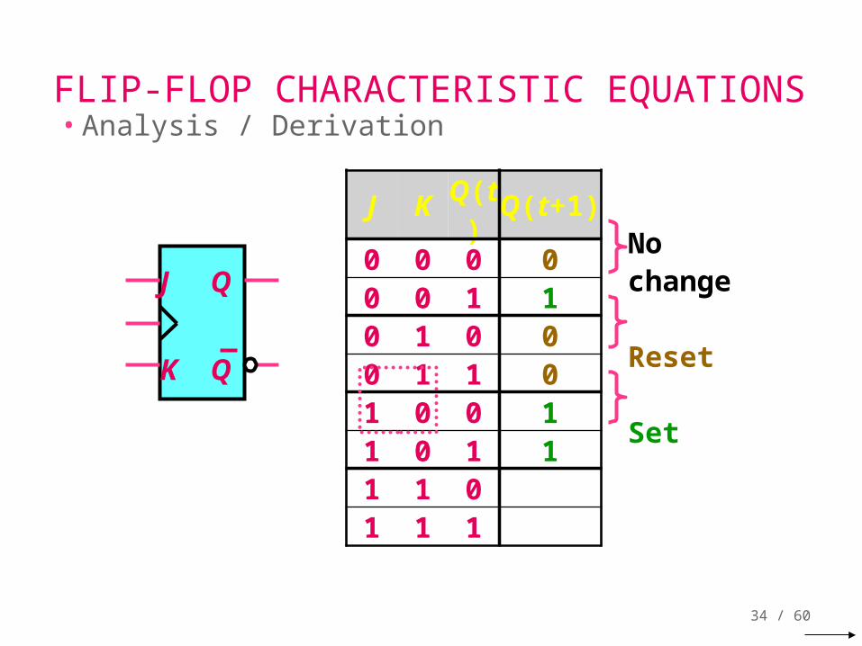
FLIP-FLOP CHARACTERISTIC EQUATIONS• Analysis / Derivation
J Q
QK
J K Q(t) Q(t+1)0 0 0 00 0 1 10 1 0 00 1 1 01 0 0 11 0 1 11 1 0 11 1 1 0
K
0 1 0 0J 1 1 0 1
Q
Q(t+1) = JQ’ + K’Q

37 / 60
FLIP-FLOPS WITH DIRECT INPUTS• Asynchronous Reset
D Q
Q
R
Reset
R’ D CLK Q(t+1)0 x x 0

38 / 60
FLIP-FLOPS WITH DIRECT INPUTS• Asynchronous Reset
D Q
Q
R
Reset
R’ D CLK Q(t+1)0 x x 01 0 ↑ 01 1 ↑ 1

39 / 60
FLIP-FLOPS WITH DIRECT INPUTS• Asynchronous Preset and Clear
PR’ CLR’ D CLK Q(t+1)1 0 x x 0D Q
Q
CLR
Reset
PR
Preset

40 / 60
FLIP-FLOPS WITH DIRECT INPUTS• Asynchronous Preset and Clear
PR’ CLR’ D CLK Q(t+1)1 0 x x 00 1 x x 1
D Q
Q
CLR
Reset
PR
Preset

41 / 60
FLIP-FLOPS WITH DIRECT INPUTS• Asynchronous Preset and Clear
PR’ CLR’ D CLK Q(t+1)1 0 x x 00 1 x x 11 1 0 ↑ 01 1 1 ↑ 1
D Q
Q
CLR
Reset
PR
Preset

42 / 60
ANALYSIS OF CLOCKED SEQUENTIAL CIRCUITS• The State
• State = Values of all Flip-Flops
Example A B = 0 0 D Q
Q
CLK
D Q
Q
A
B
y
x

43 / 60
ANALYSIS OF CLOCKED SEQUENTIAL CIRCUITS• State Equations
D Q
Q
CLK
D Q
Q
A
B
y
x
A(t+1) = DA
= A(t) x(t)+B(t) x(t) = A x + B xB(t+1) = DB
= A’(t) x(t) = A’ x y(t) = [A(t)+ B(t)] x’(t) = (A + B) x’

44 / 60
ANALYSIS OF CLOCKED SEQUENTIAL CIRCUITS
• State Table (Transition Table)D Q
Q
CLK
D Q
Q
A
B
y
x
A(t+1) = A x + B xB(t+1) = A’ x y(t) = (A + B) x’
Present State Input Next
State Output
A B x A B y0 0 00 0 10 1 00 1 11 0 01 0 11 1 01 1 1
t+1 tt
0 0 00 1 00 0 11 1 00 0 11 0 00 0 11 0 0

45 / 60
ANALYSIS OF CLOCKED SEQUENTIAL CIRCUITS
• State Table (Transition Table)D Q
Q
CLK
D Q
Q
A
B
y
x
A(t+1) = A x + B xB(t+1) = A’ x y(t) = (A + B) x’
Present State
Next State Output
x = 0 x = 1 x = 0 x = 1
A B A B A B y y0 0 0 0 0 1 0 00 1 0 0 1 1 1 01 0 0 0 1 0 1 01 1 0 0 1 0 1 0
t+1 tt

46 / 60
ANALYSIS OF CLOCKED SEQUENTIAL CIRCUITS
• State Diagram
D Q
Q
CLK
D Q
Q
A
B
y
x
0 0 1 0
0 1 1 1
0/0
0/1
1/0
1/0
1/0
1/0 0/10/1
AB input/output
Present State
Next State Output
x = 0 x = 1 x = 0 x = 1
A B A B A B y y
0 0 0 0 0 1 0 0
0 1 0 0 1 1 1 01 0 0 0 1 0 1 01 1 0 0 1 0 1 0

47 / 60
ANALYSIS OF CLOCKED SEQUENTIAL CIRCUITS• D Flip-Flops
Example:D Q
Q
x
CLK
yA
Present State Input Next
StateA x y A0 0 00 0 10 1 00 1 11 0 01 0 11 1 01 1 1
01101001
0 100,11 00,11
01,10
01,10
A(t+1) = DA = A x y

48 / 60
ANALYSIS OF CLOCKED SEQUENTIAL CIRCUITS• JK Flip-Flops
Example:J Q
QK
CLK
J Q
QK
x
A
B
JA = B KA = B x’JB = x’ KB = A x
A(t+1) = JA Q’A + K’A QA
= A’B + AB’ + AxB(t+1) = JB Q’B + K’B QB
= B’x’ + ABx + A’Bx’
Present State I/P Next
StateFlip-Flop
InputsA B x A B JA KA JB KB
0 0 00 0 10 1 00 1 11 0 01 0 11 1 01 1 1
0 0 1 00 0 0 11 1 1 01 0 0 10 0 1 10 0 0 01 1 1 11 0 0 0
0 10 01 11 01 11 00 01 1

49 / 60
ANALYSIS OF CLOCKED SEQUENTIAL CIRCUITS• JK Flip-Flops
Example:J Q
QK
CLK
J Q
QK
x
A
BPresent State I/P Next
StateFlip-Flop
InputsA B x A B JA KA JB KB
0 0 00 0 10 1 00 1 11 0 01 0 11 1 01 1 1
0 0 1 00 0 0 11 1 1 01 0 0 10 0 1 10 0 0 01 1 1 11 0 0 0
0 10 01 11 01 11 00 01 1
0 0 1 1
0 1 1 0
1 0 1
0
1
0 0
1
50 / 60
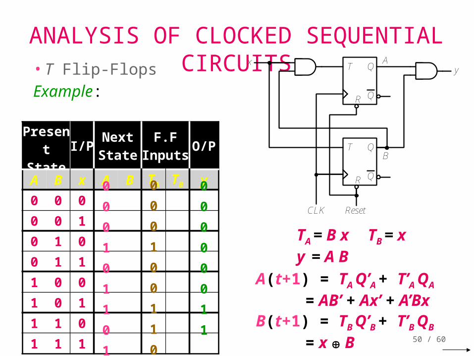
ANALYSIS OF CLOCKED SEQUENTIAL CIRCUITS• T Flip-Flops
Example:
TA = B x TB = xy = A B
A(t+1) = TA Q’A + T’A QA
= AB’ + Ax’ + A’BxB(t+1) = TB Q’B + T’B QB
= x B
A
B
T Q
QR
T Q
QR
CLK Reset
xy
Present State I/P Next
StateF.F
Inputs O/P
A B x A B TA TB y0 0 00 0 10 1 00 1 11 0 01 0 11 1 01 1 1
0 00 10 01 10 00 10 01 1
0 00 10 11 01 01 11 10 0
00000011

51 / 60
ANALYSIS OF CLOCKED SEQUENTIAL CIRCUITS• T Flip-Flops
Example:A
B
T Q
QR
T Q
QR
CLK Reset
xy
Present State I/P Next
StateF.F
Inputs O/P
A B x A B TA TB y0 0 00 0 10 1 00 1 11 0 01 0 11 1 01 1 1
0 00 10 01 10 00 10 01 1
0 00 10 11 01 01 11 10 0
00000011
0 0 0 1
1 1 1 0
0/01/0
0/0
1/0
1/0
1/1
0/00/1

52 / 60
MEALY AND MOORE MODELSPresent
State I/P Next State O/P
A B x A B y0 0 0 0 0 00 0 1 0 1 00 1 0 0 0 10 1 1 1 1 01 0 0 0 0 11 0 1 1 0 01 1 0 0 0 11 1 1 1 0 0
Mealy
For the same state,the output changes with the input
Present State I/P Next
State O/P
A B x A B y0 0 0 0 0 00 0 1 0 1 00 1 0 0 1 00 1 1 1 0 01 0 0 1 0 01 0 1 1 1 01 1 0 1 1 11 1 1 0 0 1
Moore
For the same state,the output does not change with the input

53 / 60
MOORE STATE DIAGRAMState / Output
0 0 / 0 0 1 / 0
1 1 / 1 1 0 / 0
0
1
1
1
00
01

54 / 60
TIMING DIAGRAM0 0 / 0 0 1 / 0
1 1 / 1 1 0 / 0
0 0
1
1
0 0
1
1
CLK
StateA
B
y
x
No effect
0
0
0
1
1
0
0
0
0
1
0
1
A
Bx y

55 / 60
TIMING DIAGRAM0 0 0 1
1 1 1 0
0/0 0/0
1/0
1/1
0/0 0/0
1/1
1/0
CLK
StateA
B
y
x
1
0
A
Bx y

56 / 60
DESIGN OF CLOCKED SEQUENTIAL CIRCUITS• Example:
Detect 3 or more consecutive 1’s
S0 / 0 S1 / 0
S3 / 1 S2 / 0
0
1
1
0 0
1
0
1
State A BS0 0 0S1 0 1S2 1 0S3 1 1

57 / 60
DESIGN OF CLOCKED SEQUENTIAL CIRCUITS• Example:
Detect 3 or more consecutive 1’s
Present State Input Next
State Output
A B x A B y0 0 00 0 10 1 00 1 11 0 01 0 11 1 01 1 1
0 0 00 1 00 0 01 0 00 0 01 1 00 0 11 1 1
S0 / 0 S1 / 0
S3 / 1 S2 / 0
0
1
1
0 0
1
0
1

58 / 60
DESIGN OF CLOCKED SEQUENTIAL CIRCUITS• Example:
Detect 3 or more consecutive 1’s
Present State Input Next
State Output
A B x A B y0 0 00 0 10 1 00 1 11 0 01 0 11 1 01 1 1
0 0 00 1 00 0 01 0 00 0 01 1 00 0 11 1 1
A(t+1) = DA (A, B, x) = ∑ (3, 5, 7)B(t+1) = DB (A, B, x) = ∑ (1, 5, 7)y (A, B, x) = ∑ (6, 7)
Synthesis using D Flip-Flops

59 / 60
DESIGN OF CLOCKED SEQUENTIAL CIRCUITS WITH D F.F.• Example:
Detect 3 or more consecutive 1’s
DA (A, B, x) = ∑ (3, 5, 7) = A x + B xDB (A, B, x) = ∑ (1, 5, 7) = A x + B’ xy (A, B, x) = ∑ (6, 7) = A B
Synthesis using D Flip-FlopsB
0 0 1 0A 0 1 1 0
xB
0 1 0 0A 0 1 1 0
xB
0 0 0 0A 0 0 1 1
x

60 / 60
DESIGN OF CLOCKED SEQUENTIAL CIRCUITS WITH D F.F.• Example:
Detect 3 or more consecutive 1’s
DA = A x + B xDB = A x + B’ x y = A B
Synthesis using D Flip-Flops
D Q
Q
A
CLK
x
BD Q
Q
y

61 / 60
FLIP-FLOP EXCITATION TABLESPresent
StateNext State
F.F.Input
Q(t) Q(t+1) D0 00 11 01 1
Present State
Next State
F.F.Input
Q(t) Q(t+1) J K0 00 11 01 1
0 0 (No change)0 1 (Reset)0 x
1 xx 1x 0
0101
1 0 (Set)1 1 (Toggle)0 1 (Reset)1 1 (Toggle)0 0 (No change)1 0 (Set)
Q(t) Q(t+1) T0 00 11 01 1
0110

62 / 60
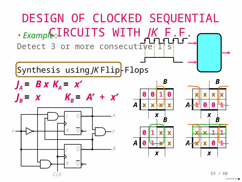
DESIGN OF CLOCKED SEQUENTIAL CIRCUITS WITH JK F.F.• Example:
Detect 3 or more consecutive 1’s
Present State Input Next
StateFlip-Flop
InputsA B x A B JA KA JB KB
0 0 0 0 00 0 1 0 10 1 0 0 00 1 1 1 01 0 0 0 01 0 1 1 11 1 0 0 01 1 1 1 1
0 x0 x0 x1 xx 1x 0x 1x 0
JA (A, B, x) = ∑ (3)dJA (A, B, x) = ∑ (4,5,6,7)KA (A, B, x) = ∑ (4, 6)dKA (A, B, x) = ∑ (0,1,2,3)JB (A, B, x) = ∑ (1, 5)dJB (A, B, x) = ∑ (2,3,6,7)KB (A, B, x) = ∑ (2, 3, 6)dKB (A, B, x) = ∑ (0,1,4,5)
Synthesis using JK F.F.
0 x1 xx 1x 10 x1 xx 1x 0
63 / 60
DESIGN OF CLOCKED SEQUENTIAL CIRCUITS WITH JK F.F.• Example:
Detect 3 or more consecutive 1’s
JA = B x KA = x’JB = x KB = A’ + x’
Synthesis using JK Flip-FlopsB
0 0 1 0A x x x x
x
B
x x x xA 1 0 0 1
xB
0 1 x xA 0 1 x x
x
B
x x 1 1A x x 0 1
x
CLK
J Q
QK
x
A
B
J Q
QK y

64 / 60
DESIGN OF CLOCKED SEQUENTIAL CIRCUITS WITH T F.F.• Example:
Detect 3 or more consecutive 1’s
Present State Input Next
StateF.F.
InputA B x A B TA TB
0 0 0 0 00 0 1 0 10 1 0 0 00 1 1 1 01 0 0 0 01 0 1 1 11 1 0 0 01 1 1 1 1
00011010
Synthesis using T Flip-Flops01110110
TA (A, B, x) = ∑ (3, 4, 6)TB (A, B, x) = ∑ (1, 2, 3, 5, 6)

65 / 60
DESIGN OF CLOCKED SEQUENTIAL CIRCUITS WITH T F.F.• Example:
Detect 3 or more consecutive 1’s
TA = A x’ + A’ B xTB = A’ B + B x
Synthesis using T Flip-Flops
B
0 0 1 0A 1 0 0 1
x
B
0 1 1 1A 0 1 0 1
x
A
B
y
T Q
Q
x
CLK
T Q
Q