21. twi – two-wire...
TRANSCRIPT
251XMEGA AU [MANUAL]8331F–AVR–04/2013
21. TWI – Two-Wire Interface
21.1 Features Bidirectional, two-wire communication interface
Phillips I2C compatible System Management Bus (SMBus) compatible
Bus master and slave operation supported Slave operation Single bus master operation Bus master in multi-master bus environment Multi-master arbitration
Flexible slave address match functions 7-bit and general call address recognition in hardware 10-bit addressing supported Address mask register for dual address match or address range masking Optional software address recognition for unlimited number of addresses
Slave can operate in all sleep modes, including power-down
Slave address match can wake device from all sleep modes
100kHz and 400kHz bus frequency support
Slew-rate limited output drivers
Input filter for bus noise and spike suppression
Support arbitration between start/repeated start and data bit (SMBus)
Slave arbitration allows support for address resolve protocol (ARP) (SMBus)
21.2 Overview
The two-wire interface (TWI) is a bidirectional, two-wire communication interface. It is I2C and System Management Bus (SMBus) compatible. The only external hardware needed to implement the bus is one pull-up resistor on each bus line.
A device connected to the bus must act as a master or a slave. The master initiates a data transaction by addressing a slave on the bus and telling whether it wants to transmit or receive data. One bus can have many slaves and one or several masters that can take control of the bus. An arbitration process handles priority if more than one master tries to transmit data at the same time. Mechanisms for resolving bus contention are inherent in the protocol.
The TWI module supports master and slave functionality. The master and slave functionality are separated from each other, and can be enabled and configured separately. The master module supports multi-master bus operation and arbitration. It contains the baud rate generator. Both 100kHz and 400kHz bus frequency is supported. Quick command and smart mode can be enabled to auto-trigger operations and reduce software complexity.
The slave module implements 7-bit address match and general address call recognition in hardware. 10-bit addressing is also supported. A dedicated address mask register can act as a second address match register or as a register for address range masking. The slave continues to operate in all sleep modes, including power-down mode. This enables the slave to wake up the device from all sleep modes on TWI address match. It is possible to disable the address matching to let this be handled in software instead.
The TWI module will detect START and STOP conditions, bus collisions, and bus errors. Arbitration lost, errors, collision, and clock hold on the bus are also detected and indicated in separate status flags available in both master and slave modes.
It is possible to disable the TWI drivers in the device, and enable a four-wire digital interface for connecting to an external TWI bus driver. This can be used for applications where the device operates from a different VCC voltage than used by the TWI bus.
252XMEGA AU [MANUAL]8331F–AVR–04/2013
21.3 General TWI Bus Concepts
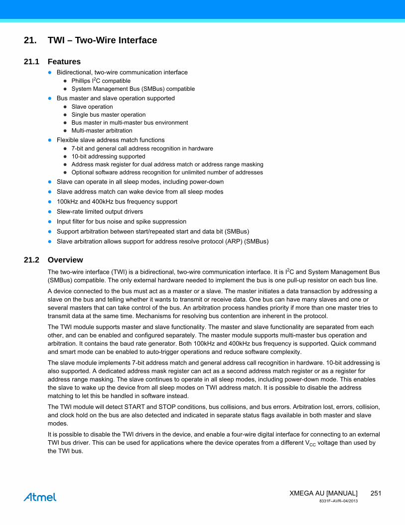
The TWI provides a simple, bidirectional, two-wire communication bus consisting of a serial clock line (SCL) and a serial data line (SDA). The two lines are open-collector lines (wired-AND), and pull-up resistors (Rp) are the only external components needed to drive the bus. The pull-up resistors provide a high level on the lines when none of the connected devices are driving the bus
The TWI bus is a simple and efficient method of interconnecting multiple devices on a serial bus. A device connected to the bus can be a master or slave, where the master controls the bus and all communication.
Figure 21-1 on page 252 illustrates the TWI bus topology.
Figure 21-1. TWI bus topology.
A unique address is assigned to all slave devices connected to the bus, and the master will use this to address a slave and initiate a data transaction.
Several masters can be connected to the same bus, called a multi-master environment. An arbitration mechanism is provided for resolving bus ownership among masters, since only one master device may own the bus at any given time.
A device can contain both master and slave logic, and can emulate multiple slave devices by responding to more than one address.
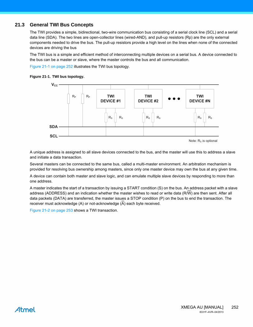
A master indicates the start of a transaction by issuing a START condition (S) on the bus. An address packet with a slave address (ADDRESS) and an indication whether the master wishes to read or write data (R/W) are then sent. After all data packets (DATA) are transferred, the master issues a STOP condition (P) on the bus to end the transaction. The receiver must acknowledge (A) or not-acknowledge (A) each byte received.
Figure 21-2 on page 253 shows a TWI transaction.
TWIDEVICE #1
RP RP
RS RS
SDA
SCL
VCC
TWIDEVICE #2
RS RS
TWIDEVICE #N
RS RS
Note: RS is optional
253XMEGA AU [MANUAL]8331F–AVR–04/2013
Figure 21-2. Basic TWI transaction diagram topology for a 7-bit address bus .
The master provides the clock signal for the transaction, but a device connected to the bus is allowed to stretch the low-level period of the clock to decrease the clock speed.
21.3.1 Electrical Characteristics
The TWI module in XMEGA devices follows the electrical specifications and timing of I2C bus and SMBus. These specifications are not 100% compliant, and so to ensure correct behavior, the inactive bus timeout period should be set in TWI master mode. Refer to “TWI Master Operation” on page 258 for more details.
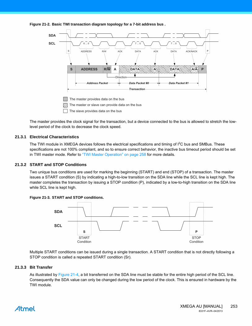
21.3.2 START and STOP Conditions
Two unique bus conditions are used for marking the beginning (START) and end (STOP) of a transaction. The master issues a START condition (S) by indicating a high-to-low transition on the SDA line while the SCL line is kept high. The master completes the transaction by issuing a STOP condition (P), indicated by a low-to-high transition on the SDA line while SCL line is kept high.
Figure 21-3. START and STOP conditions.
Multiple START conditions can be issued during a single transaction. A START condition that is not directly following a STOP condition is called a repeated START condition (Sr).
21.3.3 Bit Transfer
As illustrated by Figure 21-4, a bit transferred on the SDA line must be stable for the entire high period of the SCL line. Consequently the SDA value can only be changed during the low period of the clock. This is ensured in hardware by the TWI module.
PS ADDRESS
6 ... 0
R/W ACK ACK
7 ... 0
DATA ACK/NACK
7 ... 0
DATA
SDA
SCL
S A A/AR/WADDRESS DATA PA DATA
Address Packet Data Packet #0
Transaction
Data Packet #1
Direction
The slave provides data on the bus
The master provides data on the bus
The master or slave can provide data on the bus
SDA
SCL
STARTCondition
STOPCondition
S P
254XMEGA AU [MANUAL]8331F–AVR–04/2013
Figure 21-4. Data validity.
Combining bit transfers results in the formation of address and data packets. These packets consist of eight data bits (one byte) with the most-significant bit transferred first, plus a single-bit not-acknowledge (NACK) or acknowledge (ACK) response. The addressed device signals ACK by pulling the SCL line low during the ninth clock cycle, and signals NACK by leaving the line SCL high.
21.3.4 Address Packet
After the START condition, a 7-bit address followed by a read/write (R/W) bit is sent. This is always transmitted by the master. A slave recognizing its address will ACK the address by pulling the data line low for the next SCL cycle, while all other slaves should keep the TWI lines released and wait for the next START and address. The address, R/W bit, and acknowledge bit combined is the address packet. Only one address packet for each START condition is allowed, also when 10-bit addressing is used.
The R/W bit specifies the direction of the transaction. If the R/W bit is low, it indicates a master write transaction, and the master will transmit its data after the slave has acknowledged its address. If the R/W bit is high, it indicates a master read transaction, and the slave will transmit its data after acknowledging its address.
21.3.5 Data Packet
An address packet is followed by one or more data packets. All data packets are nine bits long, consisting of one data byte and an acknowledge bit. The direction bit in the previous address packet determines the direction in which the data are transferred.
21.3.6 Transaction
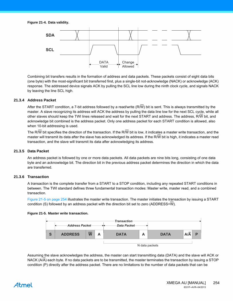
A transaction is the complete transfer from a START to a STOP condition, including any repeated START conditions in between. The TWI standard defines three fundamental transaction modes: Master write, master read, and a combined transaction.
Figure 21-5 on page 254 illustrates the master write transaction. The master initiates the transaction by issuing a START condition (S) followed by an address packet with the direction bit set to zero (ADDRESS+W).
Figure 21-5. Master write transaction.
Assuming the slave acknowledges the address, the master can start transmitting data (DATA) and the slave will ACK or NACK (A/A) each byte. If no data packets are to be transmitted, the master terminates the transaction by issuing a STOP condition (P) directly after the address packet. There are no limitations to the number of data packets that can be
SDA
SCL
DATAValid
ChangeAllowed
S A A A/A PWADDRESS DATA DATA
Address Packet Data PacketTransaction
N data packets

255XMEGA AU [MANUAL]8331F–AVR–04/2013
transferred. If the slave signals a NACK to the data, the master must assume that the slave cannot receive any more data and terminate the transaction.
Figure 21-6 on page 255 illustrates the master read transaction. The master initiates the transaction by issuing a START condition followed by an address packet with the direction bit set to one (ADDRESS+R). The addressed slave must acknowledge the address for the master to be allowed to continue the transaction.
Figure 21-6. Master read transaction.
Assuming the slave acknowledges the address, the master can start receiving data from the slave. There are no limitations to the number of data packets that can be transferred. The slave transmits the data while the master signals ACK or NACK after each data byte. The master terminates the transfer with a NACK before issuing a STOP condition.
Figure 21-7 illustrates a combined transaction. A combined transaction consists of several read and write transactions separated by repeated START conditions (Sr).
Figure 21-7. Combined Transaction.
21.3.7 Clock and Clock Stretching
All devices connected to the bus are allowed to stretch the low period of the clock to slow down the overall clock frequency or to insert wait states while processing data. A device that needs to stretch the clock can do this by holding/forcing the SCL line low after it detects a low level on the line.
Three types of clock stretching can be defined, as shown in Figure 21-8.
Figure 21-8. Clock stretching(1).
Note: 1. Clock stretching is not supported by all I2C slaves and masters.
If a slave device is in sleep mode and a START condition is detected, the clock stretching normally works during the wake-up period. For AVR XMEGA devices, the clock stretching will be either directly before or after the ACK/NACK bit, as AVR XMEGA devices do not need to wake up for transactions that are not addressed to it.
A slave device can slow down the bus frequency by stretching the clock periodically on a bit level. This allows the slave to run at a lower system clock frequency. However, the overall performance of the bus will be reduced accordingly. Both
S R A A AADDRESS DATA DATA P
TransactionAddress Packet Data Packet
N data packets
S A SrA/AR/W DATA A/A PADDRESS DATA R/WADDRESS
TransactionAddress Packet #1 N Data Packets M Data PacketsAddress Packet #2
Direction Direction
A
SDA
SCLS
ACK/NACKbit 0bit 7 bit 6
Periodic clock stretching
Random clock stretching
Wakeup clock stretching
256XMEGA AU [MANUAL]8331F–AVR–04/2013
the master and slave device can randomly stretch the clock on a byte level basis before and after the ACK/NACK bit. This provides time to process incoming or prepare outgoing data, or perform other time-critical tasks.
In the case where the slave is stretching the clock, the master will be forced into a wait state until the slave is ready, and vice versa.
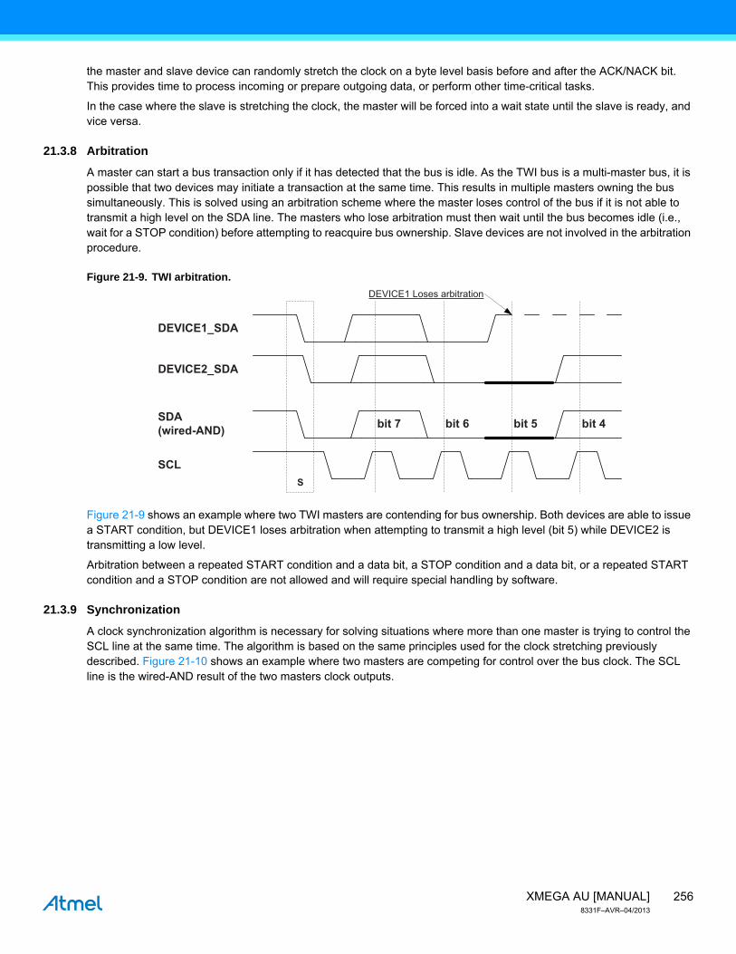
21.3.8 Arbitration
A master can start a bus transaction only if it has detected that the bus is idle. As the TWI bus is a multi-master bus, it is possible that two devices may initiate a transaction at the same time. This results in multiple masters owning the bus simultaneously. This is solved using an arbitration scheme where the master loses control of the bus if it is not able to transmit a high level on the SDA line. The masters who lose arbitration must then wait until the bus becomes idle (i.e., wait for a STOP condition) before attempting to reacquire bus ownership. Slave devices are not involved in the arbitration procedure.
Figure 21-9. TWI arbitration.
Figure 21-9 shows an example where two TWI masters are contending for bus ownership. Both devices are able to issue a START condition, but DEVICE1 loses arbitration when attempting to transmit a high level (bit 5) while DEVICE2 is transmitting a low level.
Arbitration between a repeated START condition and a data bit, a STOP condition and a data bit, or a repeated START condition and a STOP condition are not allowed and will require special handling by software.
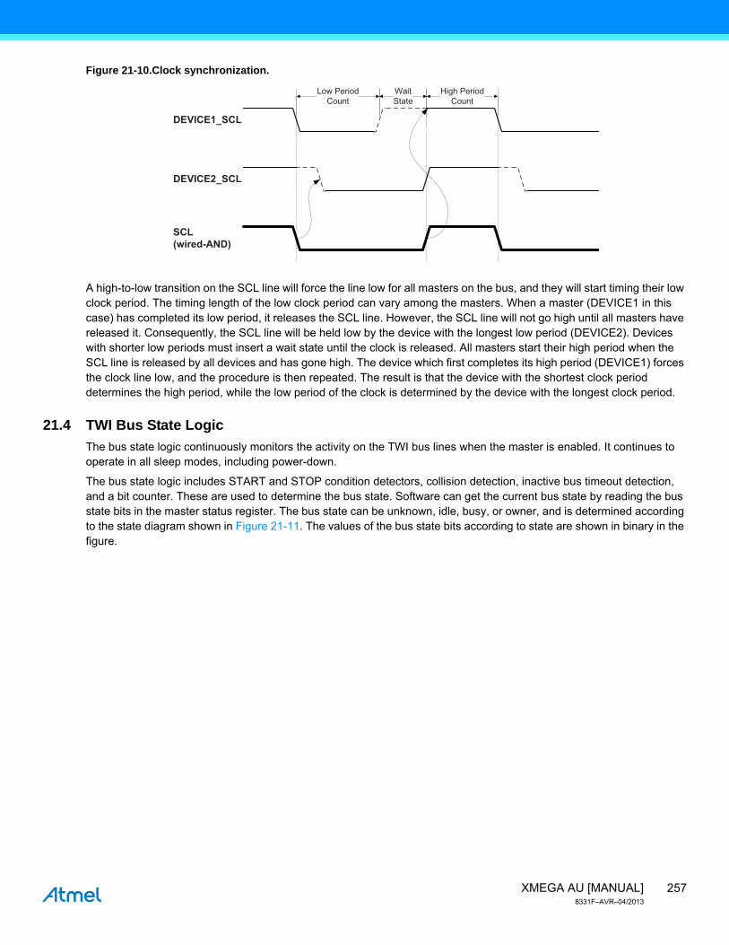
21.3.9 Synchronization
A clock synchronization algorithm is necessary for solving situations where more than one master is trying to control the SCL line at the same time. The algorithm is based on the same principles used for the clock stretching previously described. Figure 21-10 shows an example where two masters are competing for control over the bus clock. The SCL line is the wired-AND result of the two masters clock outputs.
DEVICE1_SDA
SDA(wired-AND)
DEVICE2_SDA
SCLS
bit 7 bit 6 bit 5 bit 4
DEVICE1 Loses arbitration
257XMEGA AU [MANUAL]8331F–AVR–04/2013
Figure 21-10.Clock synchronization.
A high-to-low transition on the SCL line will force the line low for all masters on the bus, and they will start timing their low clock period. The timing length of the low clock period can vary among the masters. When a master (DEVICE1 in this case) has completed its low period, it releases the SCL line. However, the SCL line will not go high until all masters have released it. Consequently, the SCL line will be held low by the device with the longest low period (DEVICE2). Devices with shorter low periods must insert a wait state until the clock is released. All masters start their high period when the SCL line is released by all devices and has gone high. The device which first completes its high period (DEVICE1) forces the clock line low, and the procedure is then repeated. The result is that the device with the shortest clock period determines the high period, while the low period of the clock is determined by the device with the longest clock period.
21.4 TWI Bus State Logic
The bus state logic continuously monitors the activity on the TWI bus lines when the master is enabled. It continues to operate in all sleep modes, including power-down.
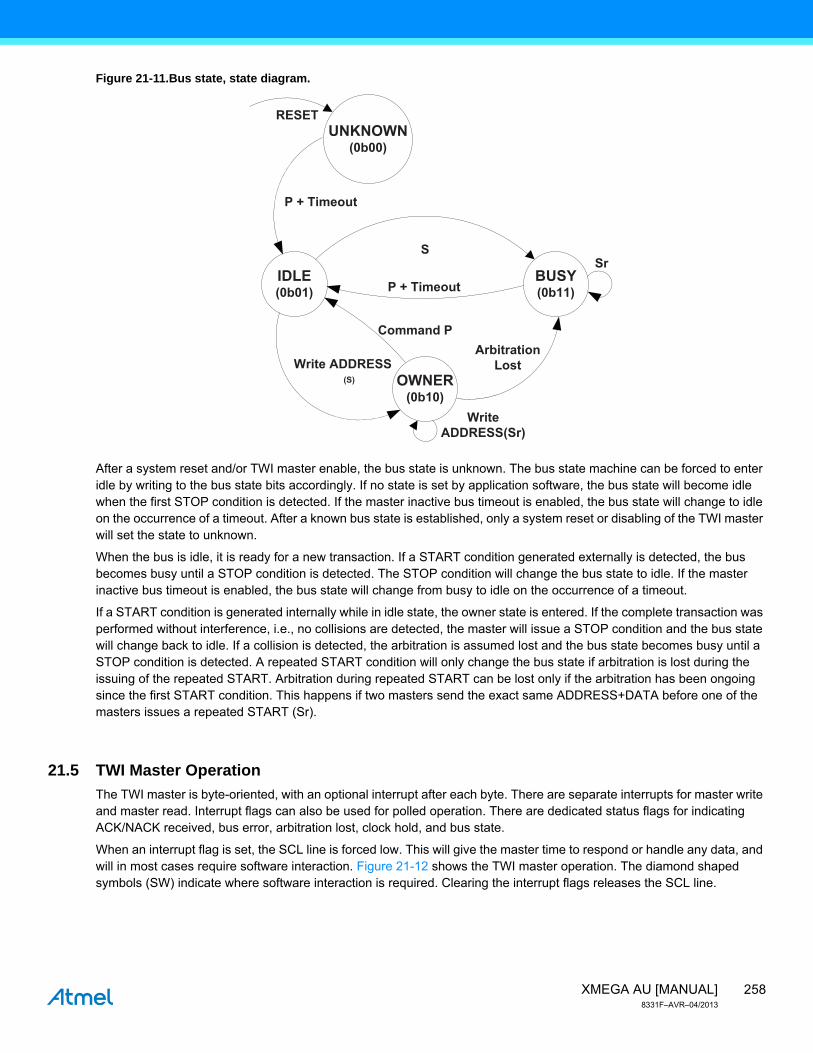
The bus state logic includes START and STOP condition detectors, collision detection, inactive bus timeout detection, and a bit counter. These are used to determine the bus state. Software can get the current bus state by reading the bus state bits in the master status register. The bus state can be unknown, idle, busy, or owner, and is determined according to the state diagram shown in Figure 21-11. The values of the bus state bits according to state are shown in binary in the figure.
DEVICE1_SCL
SCL(wired-AND)
WaitState
DEVICE2_SCL
High PeriodCount
Low PeriodCount
258XMEGA AU [MANUAL]8331F–AVR–04/2013
Figure 21-11.Bus state, state diagram.
After a system reset and/or TWI master enable, the bus state is unknown. The bus state machine can be forced to enter idle by writing to the bus state bits accordingly. If no state is set by application software, the bus state will become idle when the first STOP condition is detected. If the master inactive bus timeout is enabled, the bus state will change to idle on the occurrence of a timeout. After a known bus state is established, only a system reset or disabling of the TWI master will set the state to unknown.
When the bus is idle, it is ready for a new transaction. If a START condition generated externally is detected, the bus becomes busy until a STOP condition is detected. The STOP condition will change the bus state to idle. If the master inactive bus timeout is enabled, the bus state will change from busy to idle on the occurrence of a timeout.
If a START condition is generated internally while in idle state, the owner state is entered. If the complete transaction was performed without interference, i.e., no collisions are detected, the master will issue a STOP condition and the bus state will change back to idle. If a collision is detected, the arbitration is assumed lost and the bus state becomes busy until a STOP condition is detected. A repeated START condition will only change the bus state if arbitration is lost during the issuing of the repeated START. Arbitration during repeated START can be lost only if the arbitration has been ongoing since the first START condition. This happens if two masters send the exact same ADDRESS+DATA before one of the masters issues a repeated START (Sr).
21.5 TWI Master Operation
The TWI master is byte-oriented, with an optional interrupt after each byte. There are separate interrupts for master write and master read. Interrupt flags can also be used for polled operation. There are dedicated status flags for indicating ACK/NACK received, bus error, arbitration lost, clock hold, and bus state.
When an interrupt flag is set, the SCL line is forced low. This will give the master time to respond or handle any data, and will in most cases require software interaction. Figure 21-12 shows the TWI master operation. The diamond shaped symbols (SW) indicate where software interaction is required. Clearing the interrupt flags releases the SCL line.
P + Timeout
Write ADDRESS
IDLE(0b01)
S
BUSY(0b11)
UNKNOWN(0b00)
OWNER(0b10)
ArbitrationLost
Command P
WriteADDRESS(Sr)
Sr
(S)
RESET
P + Timeout

259XMEGA AU [MANUAL]8331F–AVR–04/2013
Figure 21-12.TWI master operation.
The number of interrupts generated is kept to a minimum by automatic handling of most conditions. Quick command and smart mode can be enabled to auto-trigger operations and reduce software complexity.
21.5.1 Transmitting Address Packets
After issuing a START condition, the master starts performing a bus transaction when the master address register is written with the 7-bit slave address and direction bit. If the bus is busy, the TWI master will wait until the bus becomes idle before issuing the START condition.
Depending on arbitration and the R/W direction bit, one of four distinct cases (M1 to M4) arises following the address packet. The different cases must be handled in software.
21.5.1.1 Case M1: Arbitration lost or bus error during address packet
If arbitration is lost during the sending of the address packet, the master write interrupt flag and arbitration lost flag are both set. Serial data output to the SDA line is disabled, and the SCL line is released. The master is no longer allowed to perform any operation on the bus until the bus state has changed back to idle.
A bus error will behave in the same way as an arbitration lost condition, but the error flag is set in addition to the write interrupt and arbitration lost flags.
21.5.1.2 Case M2: Address packet transmit complete - Address not acknowledged by slave
If no slave device responds to the address, the master write interrupt flag and the master received acknowledge flag are set. The clock hold is active at this point, preventing further activity on the bus.
21.5.1.3 Case M3: Address packet transmit complete - Direction bit cleared
If the master receives an ACK from the slave, the master write interrupt flag is set and the master received acknowledge flag is cleared. The clock hold is active at this point, preventing further activity on the bus.
IDLE S BUSYBUSY P
Sr
P
M3
M3
M2
M2
M1
M1
R DATA
ADDRESS
W
A/ADATA
Wait for IDLE
APPLICATION
SW
SW
Sr
P
M3
M2
BUSY M4ASW
A/A
A/A
A/A
M4
A
IDLE
IDLE
MASTER READ INTERRUPT + HOLD
MASTER WRITE INTERRUPT + HOLD
SW
SW
SW
BUSYR/W
SW Driver software
The master provides data on the bus
Slave provides data on the bus
A
A
R/W
BUSY M4
Bus state
Mn Diagram connections
260XMEGA AU [MANUAL]8331F–AVR–04/2013
21.5.1.4 Case M4: Address packet transmit complete - Direction bit set
If the master receives an ACK from the slave, the master proceeds to receive the next byte of data from the slave. When the first data byte is received, the master read interrupt flag is set and the master received acknowledge flag is cleared. The clock hold is active at this point, preventing further activity on the bus.
21.5.2 Transmitting Data Packets
Assuming case M3 above, the master can start transmitting data by writing to the master data register. If the transfer was successful, the slave will signal with ACK. The master write interrupt flag is set, the master received acknowledge flag is cleared, and the master can prepare new data to send. During data transfer, the master is continuously monitoring the bus for collisions.
The received acknowledge flag must be checked by software for each data packet transmitted before the next data packet can be transferred. The master is not allowed to continue transmitting data if the slave signals a NACK.
If a collision is detected and the master loses arbitration during transfer, the arbitration lost flag is set.
21.5.3 Receiving Data Packets
Assuming case M4 above, the master has already received one byte from the slave. The master read interrupt flag is set, and the master must prepare to receive new data. The master must respond to each byte with ACK or NACK. Indicating a NACK might not be successfully executed, as arbitration can be lost during the transmission. If a collision is detected, the master loses arbitration and the arbitration lost flag is set.
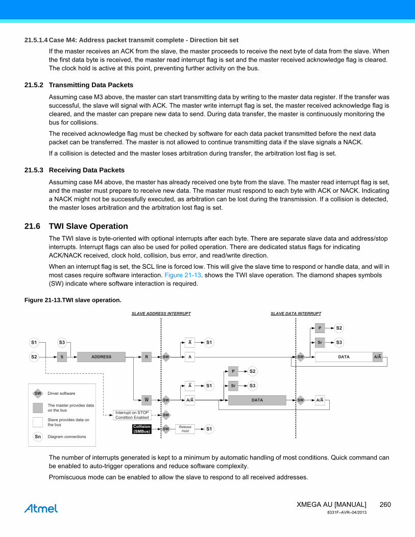
21.6 TWI Slave Operation
The TWI slave is byte-oriented with optional interrupts after each byte. There are separate slave data and address/stop interrupts. Interrupt flags can also be used for polled operation. There are dedicated status flags for indicating ACK/NACK received, clock hold, collision, bus error, and read/write direction.
When an interrupt flag is set, the SCL line is forced low. This will give the slave time to respond or handle data, and will in most cases require software interaction. Figure 21-13. shows the TWI slave operation. The diamond shapes symbols (SW) indicate where software interaction is required.
Figure 21-13.TWI slave operation.
The number of interrupts generated is kept to a minimum by automatic handling of most conditions. Quick command can be enabled to auto-trigger operations and reduce software complexity.
Promiscuous mode can be enabled to allow the slave to respond to all received addresses.
S
S3
ADDRESSS2 A
S1
R
W
DATA A/A
DATA
P S2
Sr S3
P S2
Sr S3
SLAVE ADDRESS INTERRUPT SLAVE DATA INTERRUPT
A
Collision(SMBus)
SW
SW SW
SW
A/A A/A
SW Release Hold S1
A S1
SWInterrupt on STOP Condition Enabled
S1
SW Driver software
The master provides data on the bus
Slave provides data on the bus
Sn Diagram connections
261XMEGA AU [MANUAL]8331F–AVR–04/2013
21.6.1 Receiving Address Packets
When the TWI slave is properly configured, it will wait for a START condition to be detected. When this happens, the successive address byte will be received and checked by the address match logic, and the slave will ACK a correct address and store the address in the DATA register. If the received address is not a match, the slave will not acknowledge and store address, and will wait for a new START condition.
The slave address/stop interrupt flag is set when a START condition succeeded by a valid address byte is detected. A general call address will also set the interrupt flag.
A START condition immediately followed by a STOP condition is an illegal operation, and the bus error flag is set.
The R/W direction flag reflects the direction bit received with the address. This can be read by software to determine the type of operation currently in progress.
Depending on the R/W direction bit and bus condition, one of four distinct cases (S1 to S4) arises following the address packet. The different cases must be handled in software.
21.6.1.1 Case S1: Address packet accepted - Direction bit set
If the R/W direction flag is set, this indicates a master read operation. The SCL line is forced low by the slave, stretching the bus clock. If ACK is sent by the slave, the slave hardware will set the data interrupt flag indicating data is needed for transmit. Data, repeated START, or STOP can be received after this. If NACK is sent by the slave, the slave will wait for a new START condition and address match.
21.6.1.2 Case S2: Address packet accepted - Direction bit cleared
If the R/W direction flag is cleared, this indicates a master write operation. The SCL line is forced low, stretching the bus clock. If ACK is sent by the slave, the slave will wait for data to be received. Data, repeated START, or STOP can be received after this. If NACK is sent, the slave will wait for a new START condition and address match.
21.6.1.3 Case S3: Collision
If the slave is not able to send a high level or NACK, the collision flag is set, and it will disable the data and acknowledge output from the slave logic. The clock hold is released. A START or repeated START condition will be accepted.
21.6.1.4 Case S4: STOP condition received.
When the STOP condition is received, the slave address/stop flag will be set, indicating that a STOP condition, and not an address match, occurred.
21.6.2 Receiving Data Packets
The slave will know when an address packet with R/W direction bit cleared has been successfully received. After acknowledging this, the slave must be ready to receive data. When a data packet is received, the data interrupt flag is set and the slave must indicate ACK or NACK. After indicating a NACK, the slave must expect a STOP or repeated START condition.
21.6.3 Transmitting Data Packets
The slave will know when an address packet with R/W direction bit set has been successfully received. It can then start sending data by writing to the slave data register. When a data packet transmission is completed, the data interrupt flag is set. If the master indicates NACK, the slave must stop transmitting data and expect a STOP or repeated START condition.
21.7 Enabling External Driver Interface
An external driver interface can be enabled. When this is done, the internal TWI drivers with input filtering and slew rate control are bypassed. The normal I/O pin function is used, and the direction must be configured by the user software. When this mode is enabled, an external TWI compliant tri-state driver is needed for connecting to a TWI bus.
By default, port pins 0 (Pn0) and 1 (Pn1) are used for SDA and SCL. The external driver interface uses port pins 0 to 3 for the SDA_IN, SCL_IN, SDA_OUT, and SCL_OUT signals.
262XMEGA AU [MANUAL]8331F–AVR–04/2013
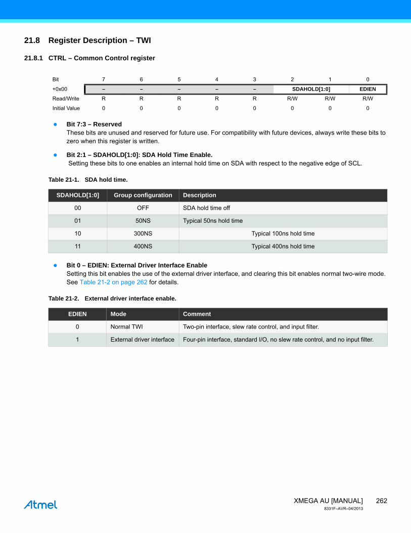
21.8 Register Description – TWI
21.8.1 CTRL – Common Control register
Bit 7:3 – ReservedThese bits are unused and reserved for future use. For compatibility with future devices, always write these bits to zero when this register is written.
Bit 2:1 – SDAHOLD[1:0]: SDA Hold Time Enable. Setting these bits to one enables an internal hold time on SDA with respect to the negative edge of SCL.
Table 21-1. SDA hold time.
Bit 0 – EDIEN: External Driver Interface EnableSetting this bit enables the use of the external driver interface, and clearing this bit enables normal two-wire mode. See Table 21-2 on page 262 for details.
Table 21-2. External driver interface enable.
Bit 7 6 5 4 3 2 1 0
+0x00 – – – – – SDAHOLD[1:0] EDIEN
Read/Write R R R R R R/W R/W R/W
Initial Value 0 0 0 0 0 0 0 0
SDAHOLD[1:0] Group configuration Description
00 OFF SDA hold time off
01 50NS Typical 50ns hold time
10 300NS Typical 100ns hold time
11 400NS Typical 400ns hold time
EDIEN Mode Comment
0 Normal TWI Two-pin interface, slew rate control, and input filter.
1 External driver interface Four-pin interface, standard I/O, no slew rate control, and no input filter.

263XMEGA AU [MANUAL]8331F–AVR–04/2013
21.9 Register Description – TWI Master
21.9.1 CTRLA – Control register A
Bit 7:6 – INTLVL[1:0]: Interrupt LevelThese bits select the interrupt level for the TWI master interrupt, as described in “Interrupts and Programmable Multilevel Interrupt Controller” on page 131.
Bit 5 – RIEN: Read Interrupt EnableSetting the read interrupt enable (RIEN) bit enables the read interrupt when the read interrupt flag (RIF) in the STATUS register is set. In addition the INTLVL bits must be nonzero for TWI master interrupts to be generated.
Bit 4 – WIEN: Write Interrupt EnableSetting the write interrupt enable (WIEN) bit enables the write interrupt when the write interrupt flag (WIF) in the STATUS register is set. In addition the INTLVL bits must be nonzero for TWI master interrupts to be generated.
Bit 3 – ENABLE: Enable TWI MasterSetting the enable TWI master (ENABLE) bit enables the TWI master.
Bit 2:0 – ReservedThese bits are unused and reserved for future use. For compatibility with future devices, always write these bits to zero when this register is written.
21.9.2 CTRLB – Control register B
Bit 7:4 – ReservedThese bits are unused and reserved for future use. For compatibility with future devices, always write these bits to zero when this register is written.
Bit 3:2 – TIMEOUT[1:0]: Inactive Bus TimeoutSetting the inactive bus timeout (TIMEOUT) bits to a nonzero value will enable the inactive bus timeout supervisor. If the bus is inactive for longer than the TIMEOUT setting, the bus state logic will enter the idle state.
Table 21-3 on page 264 lists the timeout settings.
Bit 7 6 5 4 3 2 1 0
+0x00 INTLVL[1:0] RIEN WIEN ENABLE – – –
Read/Write R/W R/W R/W R/W R/W R R R
Initial Value 0 0 0 0 0 0 0 0
Bit 7 6 5 4 3 2 1 0
+0x01 – – – – TIMEOUT[1:0] QCEN SMEN
Read/Write R R R R R/W R/W R/W R/W
Initial Value 0 0 0 0 0 0 0 0
264XMEGA AU [MANUAL]8331F–AVR–04/2013
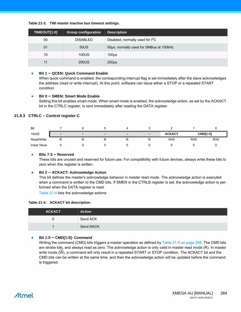
Table 21-3. TWI master inactive bus timeout settings.
Bit 1 – QCEN: Quick Command EnableWhen quick command is enabled, the corresponding interrupt flag is set immediately after the slave acknowledges the address (read or write interrupt). At this point, software can issue either a STOP or a repeated START condition.
Bit 0 – SMEN: Smart Mode EnableSetting this bit enables smart mode. When smart mode is enabled, the acknowledge action, as set by the ACKACT bit in the CTRLC register, is sent immediately after reading the DATA register.
21.9.3 CTRLC – Control register C
Bits 7:3 – ReservedThese bits are unused and reserved for future use. For compatibility with future devices, always write these bits to zero when this register is written.
Bit 2 – ACKACT: Acknowledge ActionThis bit defines the master's acknowledge behavior in master read mode. The acknowledge action is executed when a command is written to the CMD bits. If SMEN in the CTRLB register is set, the acknowledge action is per-formed when the DATA register is read.
Table 21-4 lists the acknowledge actions
Table 21-4. ACKACT bit description.
Bit 1:0 – CMD[1:0]: CommandWriting the command (CMD) bits triggers a master operation as defined by Table 21-5 on page 265. The CMD bits are strobe bits, and always read as zero. The acknowledge action is only valid in master read mode (R). In master write mode (W), a command will only result in a repeated START or STOP condition. The ACKACT bit and the CMD bits can be written at the same time, and then the acknowledge action will be updated before the command is triggered.
TIMEOUT[1:0] Group configuration Description
00 DISABLED Disabled, normally used for I2C
01 50US 50µs, normally used for SMBus at 100kHz
10 100US 100µs
11 200US 200µs
Bit 7 6 5 4 3 2 1 0
+0x02 – – – – – ACKACT CMD[1:0]
Read/Write R R R R R R/W R/W R/W
Initial Value 0 0 0 0 0 0 0 0
ACKACT Action
0 Send ACK
1 Send NACK
265XMEGA AU [MANUAL]8331F–AVR–04/2013
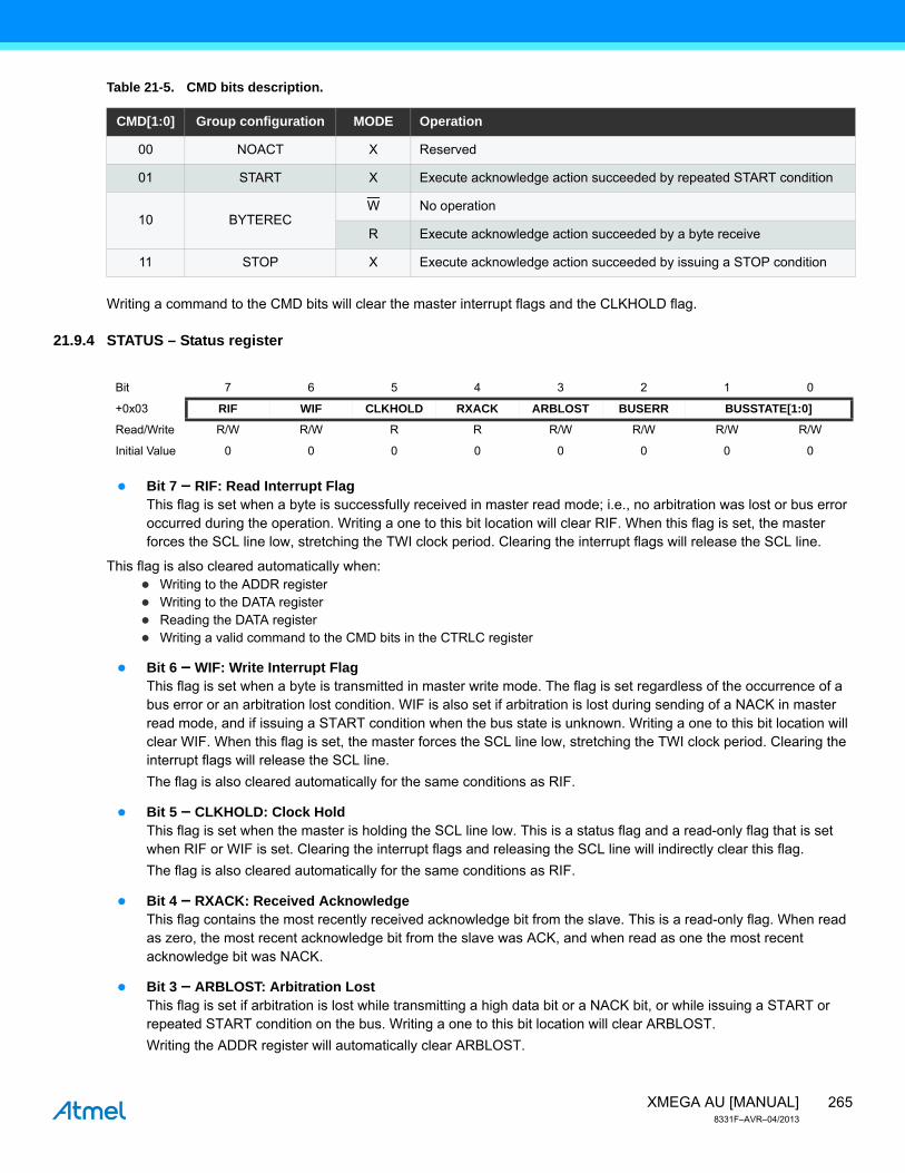
Table 21-5. CMD bits description.
Writing a command to the CMD bits will clear the master interrupt flags and the CLKHOLD flag.
21.9.4 STATUS – Status register
Bit 7 – RIF: Read Interrupt FlagThis flag is set when a byte is successfully received in master read mode; i.e., no arbitration was lost or bus error occurred during the operation. Writing a one to this bit location will clear RIF. When this flag is set, the master forces the SCL line low, stretching the TWI clock period. Clearing the interrupt flags will release the SCL line.
This flag is also cleared automatically when: Writing to the ADDR register Writing to the DATA register Reading the DATA register Writing a valid command to the CMD bits in the CTRLC register
Bit 6 – WIF: Write Interrupt FlagThis flag is set when a byte is transmitted in master write mode. The flag is set regardless of the occurrence of a bus error or an arbitration lost condition. WIF is also set if arbitration is lost during sending of a NACK in master read mode, and if issuing a START condition when the bus state is unknown. Writing a one to this bit location will clear WIF. When this flag is set, the master forces the SCL line low, stretching the TWI clock period. Clearing the interrupt flags will release the SCL line.
The flag is also cleared automatically for the same conditions as RIF.
Bit 5 – CLKHOLD: Clock HoldThis flag is set when the master is holding the SCL line low. This is a status flag and a read-only flag that is set when RIF or WIF is set. Clearing the interrupt flags and releasing the SCL line will indirectly clear this flag.
The flag is also cleared automatically for the same conditions as RIF.
Bit 4 – RXACK: Received AcknowledgeThis flag contains the most recently received acknowledge bit from the slave. This is a read-only flag. When read as zero, the most recent acknowledge bit from the slave was ACK, and when read as one the most recent acknowledge bit was NACK.
Bit 3 – ARBLOST: Arbitration LostThis flag is set if arbitration is lost while transmitting a high data bit or a NACK bit, or while issuing a START or repeated START condition on the bus. Writing a one to this bit location will clear ARBLOST.
Writing the ADDR register will automatically clear ARBLOST.
CMD[1:0] Group configuration MODE Operation
00 NOACT X Reserved
01 START X Execute acknowledge action succeeded by repeated START condition
10 BYTERECW No operation
R Execute acknowledge action succeeded by a byte receive
11 STOP X Execute acknowledge action succeeded by issuing a STOP condition
Bit 7 6 5 4 3 2 1 0
+0x03 RIF WIF CLKHOLD RXACK ARBLOST BUSERR BUSSTATE[1:0]
Read/Write R/W R/W R R R/W R/W R/W R/W
Initial Value 0 0 0 0 0 0 0 0
266XMEGA AU [MANUAL]8331F–AVR–04/2013
Bit 2 – BUSERR: Bus ErrorThis flag is set if an illegal bus condition has occurred. An illegal bus condition occurs if a repeated START or a STOP condition is detected, and the number of received or transmitted bits from the previous START condition is not a multiple of nine. Writing a one to this bit location will clear BUSERR.
Writing the ADDR register will automatically clear BUSERR.
Bit 1:0 – BUSSTATE[1:0]: Bus StateThese bits indicate the current TWI bus state as defined in Table 21-5 on page 265. The change of bus state is dependent on bus activity. Refer to the “TWI Bus State Logic” on page 257.
Table 21-6. TWI master bus state.
Writing 01 to the BUSSTATE bits forces the bus state logic into the idle state. The bus state logic cannot be forced into any other state. When the master is disabled, and after reset, the bus state logic is disabled and the bus state is unknown.
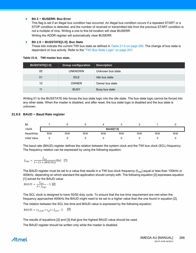
21.9.5 BAUD – Baud Rate register
The baud rate (BAUD) register defines the relation between the system clock and the TWI bus clock (SCL) frequency. The frequency relation can be expressed by using the following equation:
[1]
The BAUD register must be set to a value that results in a TWI bus clock frequency (fTWI) equal or less than 100kHz or 400kHz, depending on which standard the application should comply with. The following equation [2] expresses equation [1] solved for the BAUD value:
[2]
The SCL clock is designed to have 50/50 duty cycle. To ensure that the low time requirement are met when the frequency approaches 400kHz the BAUD might need to be set to a higher value than the one found in equation [2].
The relation between the SCL low time and BAUD value is expressed by the following equation:
[3]
The results of equations [2] and [3] that give the highest BAUD value should be used.
The BAUD register should be written only while the master is disabled.
BUSSTATE[1:0] Group configuration Description
00 UNKNOWN Unknown bus state
01 IDLE Idle bus state
10 OWNER Owner bus state
11 BUSY Busy bus state
Bit 7 6 5 4 3 2 1 0
+0x04 BAUD[7:0]
Read/Write R/W R/W R/W R/W R/W R/W R/W R/W
Initial Value 0 0 0 0 0 0 0 0
fTWI
fsys
2 ( 5 BAUD )+---------------------------------------------[Hz]=
BAUDfsys
2 fTWI------------------- 5–=
BAUD tLOW tof+ fSYS 5–=
267XMEGA AU [MANUAL]8331F–AVR–04/2013
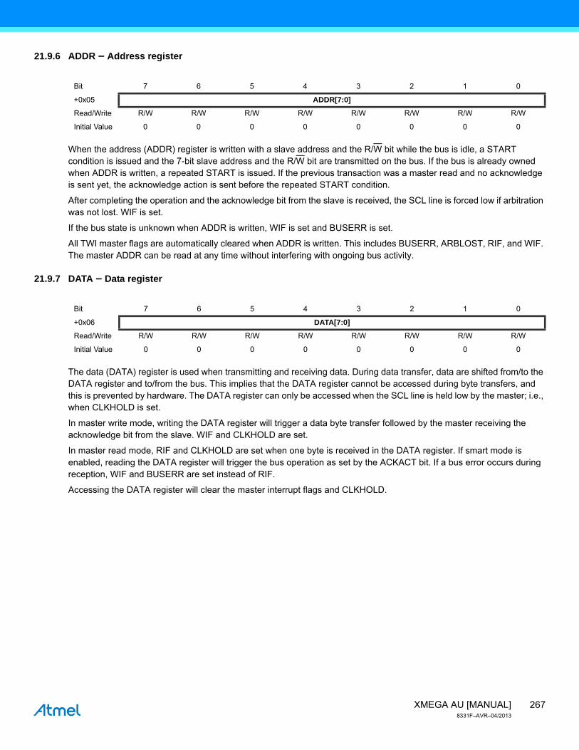
21.9.6 ADDR – Address register
When the address (ADDR) register is written with a slave address and the R/W bit while the bus is idle, a START condition is issued and the 7-bit slave address and the R/W bit are transmitted on the bus. If the bus is already owned when ADDR is written, a repeated START is issued. If the previous transaction was a master read and no acknowledge is sent yet, the acknowledge action is sent before the repeated START condition.
After completing the operation and the acknowledge bit from the slave is received, the SCL line is forced low if arbitration was not lost. WIF is set.
If the bus state is unknown when ADDR is written, WIF is set and BUSERR is set.
All TWI master flags are automatically cleared when ADDR is written. This includes BUSERR, ARBLOST, RIF, and WIF. The master ADDR can be read at any time without interfering with ongoing bus activity.
21.9.7 DATA – Data register
The data (DATA) register is used when transmitting and receiving data. During data transfer, data are shifted from/to the DATA register and to/from the bus. This implies that the DATA register cannot be accessed during byte transfers, and this is prevented by hardware. The DATA register can only be accessed when the SCL line is held low by the master; i.e., when CLKHOLD is set.
In master write mode, writing the DATA register will trigger a data byte transfer followed by the master receiving the acknowledge bit from the slave. WIF and CLKHOLD are set.
In master read mode, RIF and CLKHOLD are set when one byte is received in the DATA register. If smart mode is enabled, reading the DATA register will trigger the bus operation as set by the ACKACT bit. If a bus error occurs during reception, WIF and BUSERR are set instead of RIF.
Accessing the DATA register will clear the master interrupt flags and CLKHOLD.
Bit 7 6 5 4 3 2 1 0
+0x05 ADDR[7:0]
Read/Write R/W R/W R/W R/W R/W R/W R/W R/W
Initial Value 0 0 0 0 0 0 0 0
Bit 7 6 5 4 3 2 1 0
+0x06 DATA[7:0]
Read/Write R/W R/W R/W R/W R/W R/W R/W R/W
Initial Value 0 0 0 0 0 0 0 0

268XMEGA AU [MANUAL]8331F–AVR–04/2013
21.10 Register Description – TWI Slave
21.10.1 CTRLA – Control register A
Bit 7:6 – INTLVL[1:0]: Interrupt LevelThese bits select the interrupt level for the TWI master interrupt, as described in “Interrupts and Programmable Multilevel Interrupt Controller” on page 131.
Bit 5 – DIEN: Data Interrupt EnableSetting the data interrupt enable (DIEN) bit enables the data interrupt when the data interrupt flag (DIF) in the STA-TUS register is set. The INTLVL bits must be nonzero for the interrupt to be generated.
Bit 4 – APIEN: Address/Stop Interrupt EnableSetting the address/stop interrupt enable (APIEN) bit enables the address/stop interrupt when the address/stop interrupt flag (APIF) in the STATUS register is set. The INTLVL bits must be nonzero for interrupt to be generated.
Bit 3 – ENABLE: Enable TWI SlaveSetting this bit enables the TWI slave.
Bit 2 – PIEN: Stop Interrupt EnableSetting the this bit will cause APIF in the STATUS register to be set when a STOP condition is detected.
Bit 1 – PMEN: Promiscuous Mode EnableBy setting the this bit, the slave address match logic responds to all received addresses. If this bit is cleared, the address match logic uses the ADDR register to determine which address to recognize as its own address.
Bit 0 – SMEN: Smart Mode EnableThis bit enables smart mode. When Smart mode is enabled, the acknowledge action, as set by the ACKACT bit in the CTRLB register, is sent immediately after reading the DATA register.
21.10.2 CTRLB – Control register B
Bit 7:3 – ReservedThese bits are unused and reserved for future use. For compatibility with future devices, always write these bits to zero when this register is written.
Bit 2 – ACKACT: Acknowledge ActionThis bit defines the slave's acknowledge behavior after an address or data byte is received from the master. The acknowledge action is executed when a command is written to the CMD bits. If the SMEN bit in the CTRLA regis-ter is set, the acknowledge action is performed when the DATA register is read.
Bit 7 6 5 4 3 2 1 0
+0x00 INTLVL[1:0] DIEN APIEN ENABLE PIEN PMEN SMEN
Read/Write R/W R/W R/W R/W R/W R/W R/W R/W
Initial Value 0 0 0 0 0 0 0 0
Bit 7 6 5 4 3 2 1 0
+0x01 – – – – – ACKACT CMD[1:0]
Read/Write R R R R R R/W R/W R/W
Initial Value 0 0 0 0 0 0 0 0
269XMEGA AU [MANUAL]8331F–AVR–04/2013
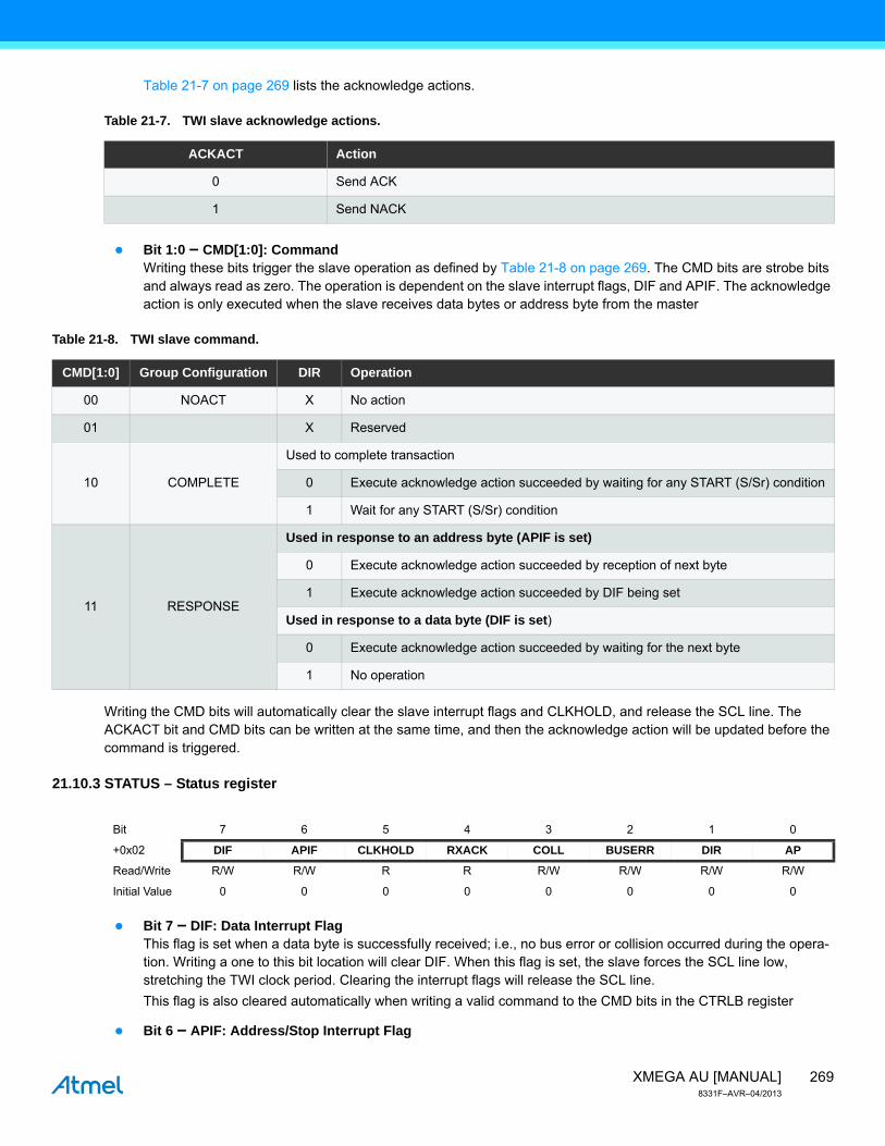
Table 21-7 on page 269 lists the acknowledge actions.
Table 21-7. TWI slave acknowledge actions.
Bit 1:0 – CMD[1:0]: CommandWriting these bits trigger the slave operation as defined by Table 21-8 on page 269. The CMD bits are strobe bits and always read as zero. The operation is dependent on the slave interrupt flags, DIF and APIF. The acknowledge action is only executed when the slave receives data bytes or address byte from the master
Table 21-8. TWI slave command.
Writing the CMD bits will automatically clear the slave interrupt flags and CLKHOLD, and release the SCL line. The ACKACT bit and CMD bits can be written at the same time, and then the acknowledge action will be updated before the command is triggered.
21.10.3 STATUS – Status register
Bit 7 – DIF: Data Interrupt FlagThis flag is set when a data byte is successfully received; i.e., no bus error or collision occurred during the opera-tion. Writing a one to this bit location will clear DIF. When this flag is set, the slave forces the SCL line low, stretching the TWI clock period. Clearing the interrupt flags will release the SCL line.
This flag is also cleared automatically when writing a valid command to the CMD bits in the CTRLB register
Bit 6 – APIF: Address/Stop Interrupt Flag
ACKACT Action
0 Send ACK
1 Send NACK
CMD[1:0] Group Configuration DIR Operation
00 NOACT X No action
01 X Reserved
10 COMPLETE
Used to complete transaction
0 Execute acknowledge action succeeded by waiting for any START (S/Sr) condition
1 Wait for any START (S/Sr) condition
11 RESPONSE
Used in response to an address byte (APIF is set)
0 Execute acknowledge action succeeded by reception of next byte
1 Execute acknowledge action succeeded by DIF being set
Used in response to a data byte (DIF is set)
0 Execute acknowledge action succeeded by waiting for the next byte
1 No operation
Bit 7 6 5 4 3 2 1 0
+0x02 DIF APIF CLKHOLD RXACK COLL BUSERR DIR AP
Read/Write R/W R/W R R R/W R/W R/W R/W
Initial Value 0 0 0 0 0 0 0 0
270XMEGA AU [MANUAL]8331F–AVR–04/2013
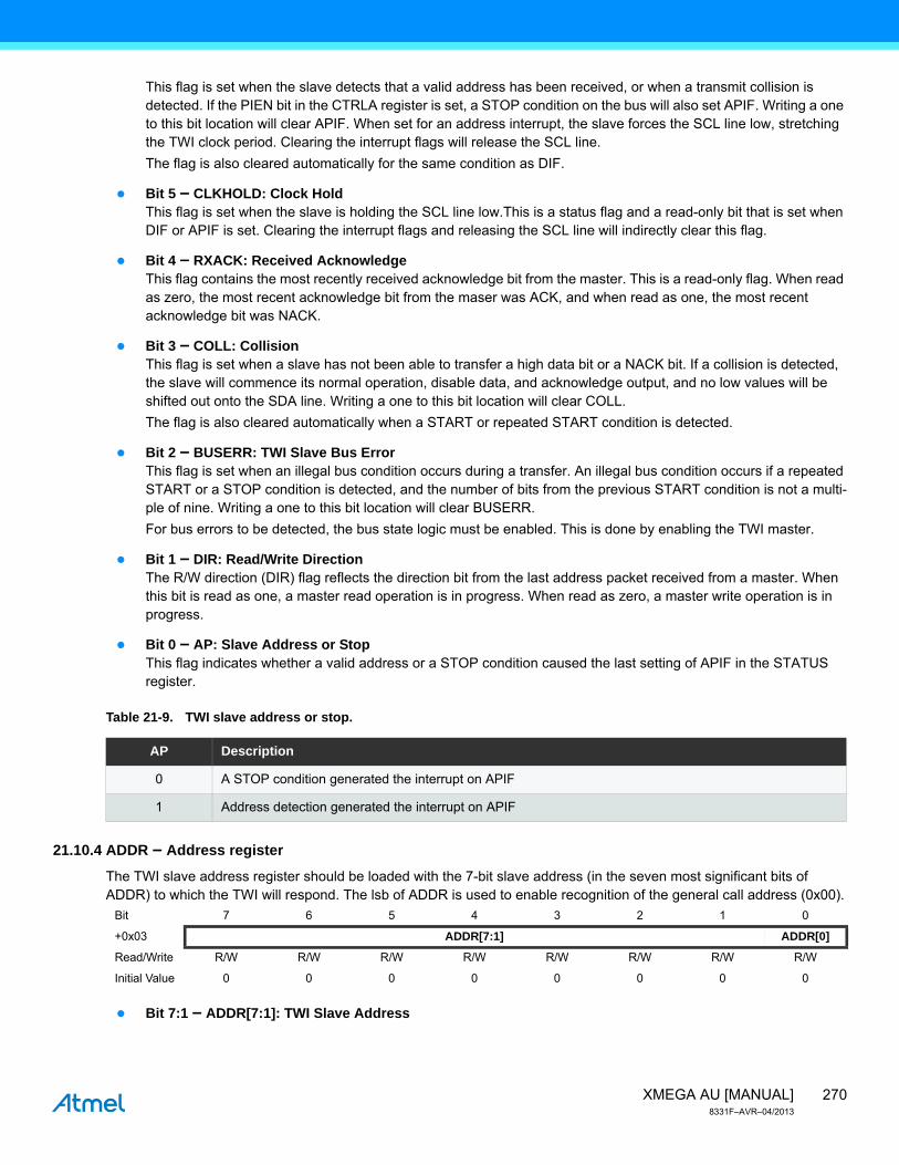
This flag is set when the slave detects that a valid address has been received, or when a transmit collision is detected. If the PIEN bit in the CTRLA register is set, a STOP condition on the bus will also set APIF. Writing a one to this bit location will clear APIF. When set for an address interrupt, the slave forces the SCL line low, stretching the TWI clock period. Clearing the interrupt flags will release the SCL line.
The flag is also cleared automatically for the same condition as DIF.
Bit 5 – CLKHOLD: Clock HoldThis flag is set when the slave is holding the SCL line low.This is a status flag and a read-only bit that is set when DIF or APIF is set. Clearing the interrupt flags and releasing the SCL line will indirectly clear this flag.
Bit 4 – RXACK: Received AcknowledgeThis flag contains the most recently received acknowledge bit from the master. This is a read-only flag. When read as zero, the most recent acknowledge bit from the maser was ACK, and when read as one, the most recent acknowledge bit was NACK.
Bit 3 – COLL: CollisionThis flag is set when a slave has not been able to transfer a high data bit or a NACK bit. If a collision is detected, the slave will commence its normal operation, disable data, and acknowledge output, and no low values will be shifted out onto the SDA line. Writing a one to this bit location will clear COLL.
The flag is also cleared automatically when a START or repeated START condition is detected.
Bit 2 – BUSERR: TWI Slave Bus ErrorThis flag is set when an illegal bus condition occurs during a transfer. An illegal bus condition occurs if a repeated START or a STOP condition is detected, and the number of bits from the previous START condition is not a multi-ple of nine. Writing a one to this bit location will clear BUSERR.
For bus errors to be detected, the bus state logic must be enabled. This is done by enabling the TWI master.
Bit 1 – DIR: Read/Write DirectionThe R/W direction (DIR) flag reflects the direction bit from the last address packet received from a master. When this bit is read as one, a master read operation is in progress. When read as zero, a master write operation is in progress.
Bit 0 – AP: Slave Address or StopThis flag indicates whether a valid address or a STOP condition caused the last setting of APIF in the STATUS register.
Table 21-9. TWI slave address or stop.
21.10.4 ADDR – Address register
The TWI slave address register should be loaded with the 7-bit slave address (in the seven most significant bits of ADDR) to which the TWI will respond. The lsb of ADDR is used to enable recognition of the general call address (0x00).
Bit 7:1 – ADDR[7:1]: TWI Slave Address
AP Description
0 A STOP condition generated the interrupt on APIF
1 Address detection generated the interrupt on APIF
Bit 7 6 5 4 3 2 1 0
+0x03 ADDR[7:1] ADDR[0]
Read/Write R/W R/W R/W R/W R/W R/W R/W R/W
Initial Value 0 0 0 0 0 0 0 0
271XMEGA AU [MANUAL]8331F–AVR–04/2013
This register contains the TWI slave address used by the slave address match logic to determine if a master has addressed the slave. The seven most-significant bits (ADDR[7:1]) represent the slave address.
When using 10-bit addressing, the address match logic only supports hardware address recognition of the first byte of a 10-bit address. By setting ADDR[7:1] = 0b11110nn, ”nn” represents bits 9 and 8 of the slave address. The next byte received is bits 7 to 0 in the 10-bit address, and this must be handled by software.
When the address match logic detects that a valid address byte is received, APIF is set and the DIR flag is updated.
If the PMEN bit in CTRLA is set, the address match logic responds to all addresses transmitted on the TWI bus. The ADDR register is not used in this mode.
Bit 0 – ADDR: General Call Recognition EnableWhen ADDR[0] is set, this enables general call address recognition logic so the device can respond to a general address call that addresses all devices on the bus.
21.10.5 DATA – Data register
The data (DATA) register is used when transmitting and received data. During data transfer, data are shifted from/to the DATA register and to/from the bus. This implies that the DATA register cannot be accessed during byte transfers, and this is prevented by hardware. The DATA register can be accessed only when the SCL line is held low by the slave; i.e., when CLKHOLD is set.
When a master is reading data from the slave, data to send must be written to the DATA register. The byte transfer is started when the master starts to clock the data byte from the slave, followed by the slave receiving the acknowledge bit from the master. DIF and CLKHOLD are set.
When a master writes data to the slave, DIF and CLKHOLD are set when one byte has been received in the DATA register. If smart mode is enabled, reading the DATA register will trigger the bus operation as set by the ACKACT bit.
Accessing the DATA register will clear the slave interrupt flags and CLKHOLD. When an address match occurs, the received address will be stored in the DATA register.
21.10.6 ADDRMASK – Address Mask register
Bit 7:1 – ADDRMASK[7:1]: Address MaskThese bits can act as a second address match register or as an address mask register, depending on the ADDREN setting.
If ADDREN is set to zero, ADDRMASK can be loaded with a 7-bit slave address mask. Each bit in ADDRMASK can mask (disable) the corresponding address bit in the ADDR register. If the mask bit is one, the address match between the incoming address bit and the corresponding bit in ADDR is ignored; i.e., masked bits will always match.
If ADDREN is set to one, ADDRMASK can be loaded with a second slave address in addition to the ADDR regis-ter. In this mode, the slave will match on two unique addresses, one in ADDR and the other in ADDRMASK.
Bit 7 6 5 4 3 2 1 0
+0x04 DATA[7:0]
Read/Write R/W R/W R/W R/W R/W R/W R/W R/W
Initial Value 0 0 0 0 0 0 0 0
Bit 7 6 5 4 3 2 1 0
+0x05 ADDRMASK[7:1] ADDREN
Read/Write R/W R/W R/W R/W R/W R/W R/W R/W
Initial Value 0 0 0 0 0 0 0 0
272XMEGA AU [MANUAL]8331F–AVR–04/2013
Bit 0 – ADDREN: Address EnableBy default, this bit is zero, and the ADDRMASK bits acts as an address mask to the ADDR register. If this bit is set to one, the slave address match logic responds to the two unique addresses in ADDR and ADDRMASK.
21.11 Register summary – TWI
21.12 Register summary – TWI master
21.13 Register summary – TWI slave
21.14 Interrupt vector summary
Table 21-10. TWI interrupt vectors and their word offset addresses.
Address Name Bit 7 Bit 6 Bit 5 Bit 4 Bit 3 Bit 2 Bit 1 Bit 0 Page
+0x00 CTRL – – – – – SDAHOLD EDIEN 262
+0x01 MASTER Offset address for TWI Master
+0x08 SLAVE Offset address for TWI Slave
Address Name Bit 7 Bit 6 Bit 5 Bit 4 Bit 3 Bit 2 Bit 1 Bit 0 Page
+0x00 CTRLA INTLVL[1:0] RIEN WIEN ENABLE – – – 263
+0x01 CTRLB – – – – TIMEOUT[1:0] QCEN SMEN 263
+0x02 CTRLC – – – – – ACKACT CMD[1:0] 264
+0x03 STATUS RIF WIF CLKHOLD RXACK ARBLOST BUSERR BUSSTATE[1:0] 265
+0x04 BAUD BAUD[7:0] 266
+0x05 ADDR ADDR[7:0] 267
+0x06 DATA DATA[7:0] 267
Address Name Bit 7 Bit 6 Bit 5 Bit 4 Bit 3 Bit 2 Bit 1 Bit 0 Page
+0x00 CTRLA INTLVL[1:0] DIEN APIEN ENABLE PIEN TPMEN SMEN 268
+0x01 CTRLB – – – – – ACKACT CMD[1:0] 268
+0x02 STATUS DIF APIF CLKHOLD RXACK COLL BUSERR DIR AP 269
+0x03 ADDR ADDR[7:0] 270
+0x04 DATA DATA[7:0] 271
+0x05 ADDRMASK ADDRMASK[7:1] ADDREN 271
Offset Source Interrupt description
0x00 SLAVE_vect TWI slave interrupt vector
0x02 MASTER_vect TWI master interrupt vector