sbos187a – october 2001 4-20ma, two-wire ... two-wire transmitter “smart” programmable with...
TRANSCRIPT
4-20mA, TWO-WIRE TRANSMITTER“Smart” Programmable with Signal Conditioning
FEATURES COMPLETE TRANSMITTER + RTD
LINEARIZATION
TWO-WIRE, 4-20mA OUTPUT
VOLTAGE OUTPUT (0.5V to 4.5V)
ELIMINATES POTENTIOMETERS ANDTRIMMING
DIGITALLY CALIBRATED
5V SUB-REGULATOR OUTPUT
SERIAL SPI BUS INTERFACE
SSOP-24 PACKAGESPI is a registered trademark of Motorola.
APPLICATIONS REMOTE RTD TRANSMITTERS
PRESSURE BRIDGE TRANSMITTERS
STRAIN GAGE TRANSMITTERS
SCADA REMOTE DATA ACQUISITION
WEIGHING SYSTEMS
INDUSTRIAL PROCESS CONTROL
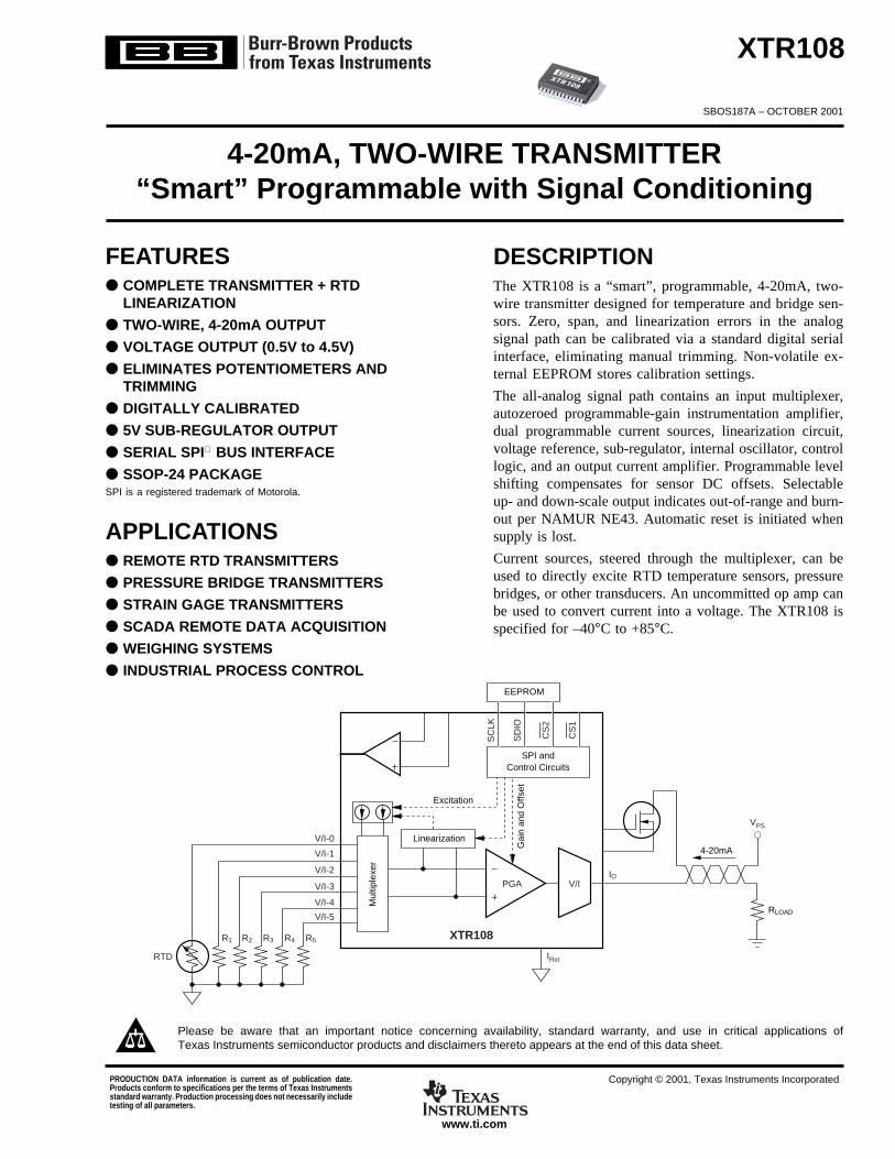
DESCRIPTIONThe XTR108 is a “smart”, programmable, 4-20mA, two-wire transmitter designed for temperature and bridge sen-sors. Zero, span, and linearization errors in the analogsignal path can be calibrated via a standard digital serialinterface, eliminating manual trimming. Non-volatile ex-ternal EEPROM stores calibration settings.
The all-analog signal path contains an input multiplexer,autozeroed programmable-gain instrumentation amplifier,dual programmable current sources, linearization circuit,voltage reference, sub-regulator, internal oscillator, controllogic, and an output current amplifier. Programmable levelshifting compensates for sensor DC offsets. Selectableup- and down-scale output indicates out-of-range and burn-out per NAMUR NE43. Automatic reset is initiated whensupply is lost.
Current sources, steered through the multiplexer, can beused to directly excite RTD temperature sensors, pressurebridges, or other transducers. An uncommitted op amp canbe used to convert current into a voltage. The XTR108 isspecified for –40°C to +85°C.
SBOS187A – OCTOBER 2001
XTR108
www.ti.com
PRODUCTION DATA information is current as of publication date.Products conform to specifications per the terms of Texas Instrumentsstandard warranty. Production processing does not necessarily includetesting of all parameters.
Copyright © 2001, Texas Instruments Incorporated
Please be aware that an important notice concerning availability, standard warranty, and use in critical applications ofTexas Instruments semiconductor products and disclaimers thereto appears at the end of this data sheet.
XTR108
SPI andControl Circuits
4-20mA
EEPROM
Linearization
Excitation
IO
IRet
Mul
tiple
xer
Gai
n an
d O
ffset
SD
IO
SC
LK
CS
2
CS
1
V/I-0
V/I-1
V/I-2
V/I-3
V/I-4
V/I-5
RTD
R1 R2 R3 R4 R5
PGA V/I
VPS
RLOAD
XTR108
XTR1082SBOS187Awww.ti.com
Loop Supply Voltage, VPS ............................ Dependent on External FET
XTR Supply Voltage, External VS (Referenced to IRET Pin) ............ +5.5V
Input Voltage to Multiplexer (Referenced to IRET Pin) ................ 0V to VS
Output Current Limit ................................................................ Continuous
Storage Temperature Range .........................................–55°C to +125°C
Junction Temperature .................................................................... +165°C
Lead Temperature (soldering, 10s) ............................................... +300°C
ABSOLUTE MAXIMUM RATINGS ELECTROSTATICDISCHARGE SENSITIVITY
This integrated circuit can be damaged by ESD. Texas Instru-ments recommends that all integrated circuits be handled withappropriate precautions. Failure to observe proper handlingand installation procedures can cause damage.
ESD damage can range from subtle performance degradationto complete device failure. Precision integrated circuits maybe more susceptible to damage because very small parametricchanges could cause the device not to meet its publishedspecifications.
SPECIFIEDPACKAGE TEMPERATURE PACKAGE ORDERING TRANSPORT
PRODUCT PACKAGE-LEAD DESIGNATOR RANGE MARKING NUMBER(1) MEDIA, QUANTITY
XTR108EA SSOP-24 DBQ –40°C to +85°C XTR108EA XTR108EA Rails" " " " " XTR108EA/2K5 Tape and Reel, 2500
NOTE: (1) Models with a slash (/) are available only in Tape and Reel in the quantities indicated (e.g., / 2K5 indicates 2500 devices per reel). Ordering 2500 piecesof “XTR108EA/2K5” will get a single 2500-piece Tape and Reel.
PACKAGE/ORDERING INFORMATION
ELECTRICAL CHARACTERISTICSBoldface limits apply over the specified temperature range, TA = –40°C to +85°C.At TA = +25°C, VPS = 24V, and Supertex DN2540 external depletion-mode FET transistor, unless otherwise noted, all voltages measured with respect to IRET pin.
XTR108EA
PARAMETER CONDITIONS MIN TYP MAX UNITS
VIN TO IOUT TRANSFER FUNCTION IO = VIN (Span) + 4mAOutput
Specified Range 4 20 mAOver-Scale Limit Resolution Digital Select: 21-28.5mA 0.5 mAFault Over-Scale Level(1) Above Over-Scale Selected +1.0 mAUnder-Scale Limit Resolution Digital Select: 2.2-3.6mA 0.2 mAFault Under-Scale Level(1) Below Under-Scale Selected –0.4 mA
Output for Zero InputZero Error, Unadjusted VIN = 0V ±50 µA
vs Temperature ±0.2 ±1.5 µA/°Cvs Loop-Supply Voltage, VLOOP VLOOP = 7.5V to 24V 0.02 µA/Vvs Common-Mode Voltage VCM = 0.2V to 3.5V ±1 µA/V
Adjustment Resolution, Zero Input 1.8 µA/StepAdjustment Range, Zero Input ±4 mA
Span(2) Span = IO/VIN
Initial, Unadjusted ±1 %Drift (vs Temperature) 40 ppm/°CSpan Adjustment Resolution 0.05 %Span Adjustment Range
PGA + Output Amplifier(3) RVI = 6.34kΩ 49.3 3150 mA/VNonlinearity, Ideal Input Full-Scale VIN = 50mV 0.01 %
PGAAutozeroing Internal Frequency 6.5 kHzPGA Offset Voltage (RTI)(4) VCM = 1V ±10 ±50 µV
vs Temperature ±0.02 µV/°Cvs Supply Voltage, VS VS = 4.5V to 5.5V ±0.5 µV/Vvs Common-Mode Voltage VCM = 0.2V to 3.5V 105 dB
Common-Mode Input Range 0.2 VS – 1.5 VInput Bias Current 50 pA
vs Temperature Doubles/10°C pAInput Offset Current 10 pA
vs Temperature Doubles/10°C pA
XTR108 3SBOS187A www.ti.com
ELECTRICAL CHARACTERISTICS (Cont.)
Boldface limits apply over the specified temperature range, TA = –40°C to +85°C.At TA = +25°C, VPS = 24V, and Supertex DN2540 external depletion-mode FET transistor, unless otherwise noted, all voltages measured with respect to IRET pin.
XTR108EA
PARAMETER CONDITIONS MIN TYP MAX UNITS
PGA (Cont.)Input Impedance: Differential 30 || 6 GΩ || pFInput Impedance: Common-Mode 50 || 20 GΩ || pFVoltage Noise, 0.1Hz to 10Hz 6 µVp-p
PGA GainGain Range Steps 6.25, 12.5, 25, 50, 100, 200, 400 6.25 400 V/VInitial Error Gain = 6.25, 12.5, 25, 50 ±0.5 ±2.5 %
G = 100, 200 ±0.5 ±3 %G = 400 ±0.8 ±3.5 %
vs Temperature ±30 ppm/°COutput Voltage Range(5) RLOAD = 6.34kΩ to IRET 0.2 4.5 V
Typical Operating Range for 4-20mA XTR Output 0.5 to 2.5 VCapacitive Drive 200 pFShort-Circuit Current +6/–9 mA
ZERO OFFSET DACSZero-Code Output Level VCM = 1V, VIN = 0V
RTO(6) of Current Amplifier RV/I = 6.34kΩ 4.116 mARTO(6) of PGA 522 mV
Coarse DAC, 256 Steps 7 Bits + SignAdjustment Range Relative to Zero-Code Level
RTO(6) of Current Amplifier –3.77 to +3.77 mARTO(6) of PGA –470 to +470 mV
Step SizeRTO(6) of Current Amplifier 0.029 mARTO(6) of PGA 3.7 mV
Linearity ±0.5 LSBFine DAC, 256 Steps Relative to Zero-Code Level 7 Bits + Sign
Adjustment RangeRTO(6) of Current Amplifier –236 to +236 µARTO(6) of PGA –29.4 to +29.4 mV
Step SizeRTO(6) of Current Amplifier 0.0018 mARTO(6) of PGA 0.23 mV
Linearity ±1 LSBNoise, RTO(6) f = 0.1Hz to 10Hz 1.1 µAp-p
CURRENT AMPLIFIERCurrent Gain 49 50 51 A/ACurrent Gain Drift 10 ppm/°C
CURRENT SOURCES, IREF1 AND IREF2Zero-Code Output Level, Each RSET = 12.1kΩ 480 493 510 µACoarse DAC, 256 Steps 7 Bits + Sign
Adjustment Range(7) –195 to +195 µAStep Size 1.54 µA
Fine DAC, 256 Steps 7 Bits + SignAdjustment Range(7) –12.2 to +12.2 µAStep Size 96 nA
LinearityCoarse ±0.2 LSBFine ±0.5 LSBvs Temperature ±35 ppm/°C
Matching ±0.2 %vs Temperature ±10 ppm/°C
Compliance Voltage, Positive(5) VS – 2 VS – 1.5 VOutput Impedance 100 MΩCurrent Noise f = 0.1Hz to 10Hz 0.015 µAp-p
LINEARIZATION DACLinearization Range, 256 Steps 8 BitsMax Linearization Coefficient ∆IREF/∆VIN, RLIN = 15.8kΩ 0.99 µA/mV
Step Size 3.9 nA/mV
SUB REGULATOR, VS Supply Voltage for XTRVoltage 4.8 5.1 5.4 V
vs Temperature ±50 ppm/°Cvs Loop-Supply Voltage VLOOP = 7.5V to 24V ±0.03 mV/V
XTR1084SBOS187Awww.ti.com
XTR108EA
PARAMETER CONDITIONS MIN TYP MAX UNITS
ELECTRICAL CHARACTERISTICS (Cont.)
Boldface limits apply over the specified temperature range, TA = –40°C to +85°C.At TA = +25°C, VPS = 24V, and Supertex DN2540 external depletion-mode FET transistor, unless otherwise noted, all voltages measured with respect to IRET pin.
NOTES: (1) Over-scale and under-scale complies with NAMUR NE43 recommendation. (2) Span adjustment is determined by PGA gain and sensorexcitation. (3) Span can be digitally adjusted in three ways: PGA gain, current reference Coarse, and current reference Fine. (4) RTI = Referred to Input.(5) Current source output voltage measured with respect to IRET. (6) RTO = Referred to Output. (7) Excitation DAC range sufficient to adjust span fullybetween PGA gain steps. (8) Output current into external circuitry is limited by an external MOS power FET. (9) Measured with over- and under-scale limitsdisabled.
OVER- AND UNDER-SCALE LIMITINGOver-Scale DAC: 16 Steps 4 Bits
Adjustment RangeRTO(6) of Current Amplifier RVI = 6.34kΩ 20.7 to 28.1 mARTO(6) of PGA 2.625 to 3.563 V
Step SizeRTO(6) of Current Amplifier 0.49 mARTO(6) of PGA 62.5 mV
Accuracy ±10 %Under-Scale DAC: 8 Steps 3 Bits
Adjustment RangeRTO(6) of Current Amplifier RVI = 6.34kΩ 2.17 to 3.55 mARTO(6) of PGA 275 to 450 mV
Step SizeRTO(6) of Current Amplifier 0.195 mARTO(6) of PGA 25 mV
Accuracy ±5 %
VOLTAGE REFERENCE, VREF
Internal Bandgap 1.193 Vvs Temperature ±5 ±50 ppm/°C
UNCOMMITTED OP AMPInput
Offset Voltage VCM = 2V ±2 mVvs Temperature ±3 µV/°Cvs Common-Mode Voltage 90 dB
Open-Loop Gain 110 dBCommon-Mode Input Range 0 to 3.5 VOutput Voltage Range RL = 10kΩ to VS/2 0.2 VS – 0.2 V
DIGITAL INPUT/OUTPUTLogic Family CMOSLogic Levels
VIL 0 0.8 VVIH 3.5 VS VVOL IOL = 300µA 0.4 VVOH IOH = –300µA VS – 1 V
Input CurrentIIH (CS1) 3.5 < VIN < VS –200 –120 10 µAIIL (CS1) 0 < VIN < 0.8 –20 –6 10 µAIIH, IIL (SCLK, DIO) 0 < VIN < VS –20 –6 10 µA
INTERNAL OSCILLATORFrequency, fOSC 210 kHz
TEMPERATURE RANGESpecification –40 +85 °COperating –55 +125 °CθJA, Junction to Ambient 100 °C/W
LOOP SUPPLYVoltage Range with Supertex DN2540 7.5 VQuiescent Current RSET Open, LINReg = 0, No Sensor Current(8)(9) 0.5 mA
XTR108 5SBOS187A www.ti.com
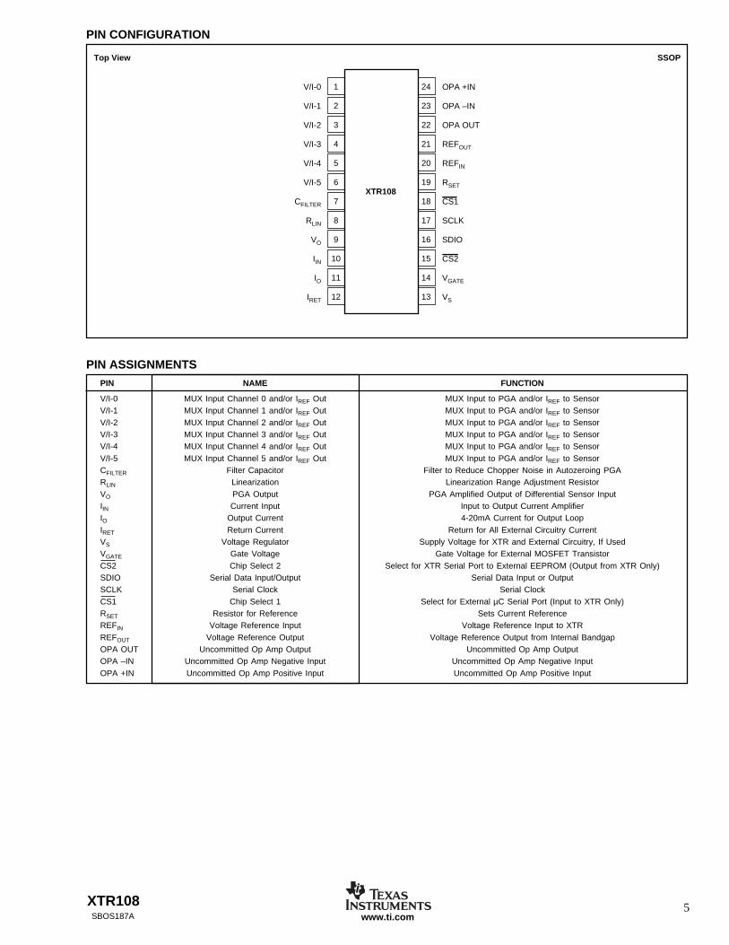
Top View SSOP
PIN CONFIGURATION
V/I-0
V/I-1
V/I-2
V/I-3
V/I-4
V/I-5
CFILTER
RLIN
VO
IIN
IO
IRET
XTR108
OPA +IN
OPA –IN
OPA OUT
REFOUT
REFIN
RSET
CS1
SCLK
SDIO
CS2
VGATE
VS
1
2
3
4
5
6
7
8
9
10
11
12
24
23
22
21
20
19
18
17
16
15
14
13
PIN ASSIGNMENTSPIN NAME FUNCTION
V/I-0 MUX Input Channel 0 and/or IREF Out MUX Input to PGA and/or IREF to SensorV/I-1 MUX Input Channel 1 and/or IREF Out MUX Input to PGA and/or IREF to SensorV/I-2 MUX Input Channel 2 and/or IREF Out MUX Input to PGA and/or IREF to SensorV/I-3 MUX Input Channel 3 and/or IREF Out MUX Input to PGA and/or IREF to SensorV/I-4 MUX Input Channel 4 and/or IREF Out MUX Input to PGA and/or IREF to SensorV/I-5 MUX Input Channel 5 and/or IREF Out MUX Input to PGA and/or IREF to SensorCFILTER Filter Capacitor Filter to Reduce Chopper Noise in Autozeroing PGARLIN Linearization Linearization Range Adjustment ResistorVO PGA Output PGA Amplified Output of Differential Sensor InputIIN Current Input Input to Output Current AmplifierIO Output Current 4-20mA Current for Output LoopIRET Return Current Return for All External Circuitry CurrentVS Voltage Regulator Supply Voltage for XTR and External Circuitry, If UsedVGATE Gate Voltage Gate Voltage for External MOSFET TransistorCS2 Chip Select 2 Select for XTR Serial Port to External EEPROM (Output from XTR Only)SDIO Serial Data Input/Output Serial Data Input or OutputSCLK Serial Clock Serial ClockCS1 Chip Select 1 Select for External µC Serial Port (Input to XTR Only)RSET Resistor for Reference Sets Current ReferenceREFIN Voltage Reference Input Voltage Reference Input to XTRREFOUT Voltage Reference Output Voltage Reference Output from Internal BandgapOPA OUT Uncommitted Op Amp Output Uncommitted Op Amp OutputOPA –IN Uncommitted Op Amp Negative Input Uncommitted Op Amp Negative InputOPA +IN Uncommitted Op Amp Positive Input Uncommitted Op Amp Positive Input
XTR1086SBOS187Awww.ti.com
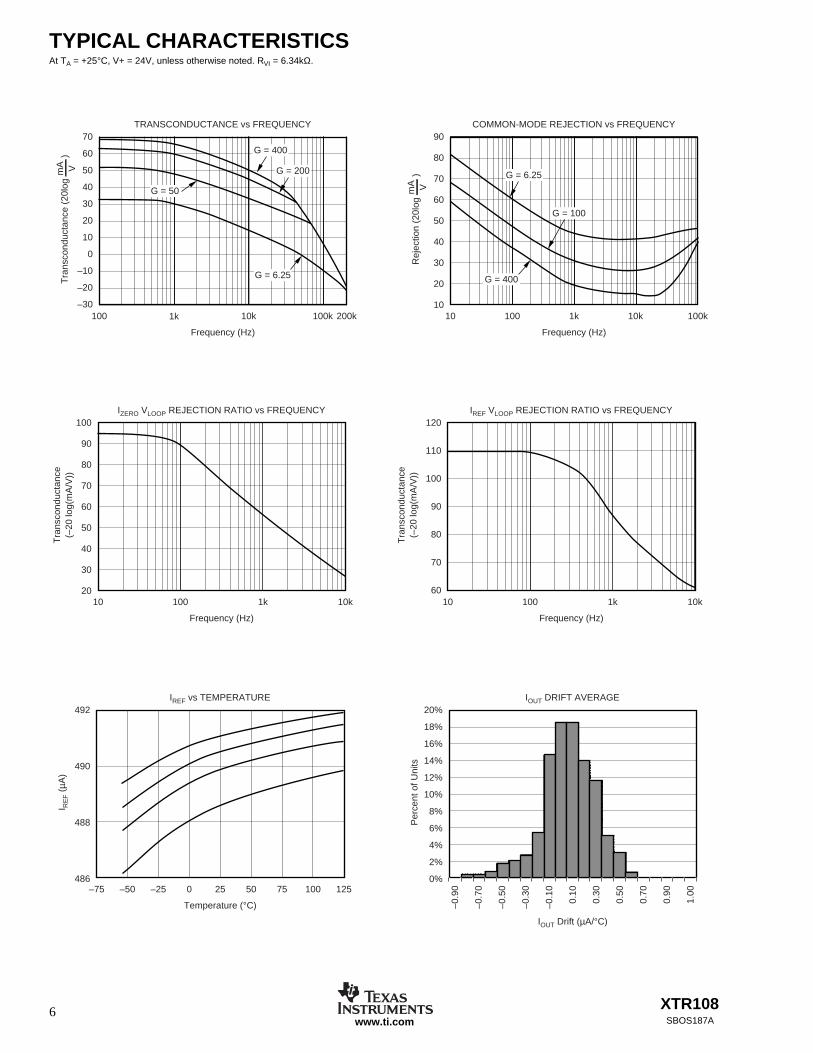
TYPICAL CHARACTERISTICSAt TA = +25°C, V+ = 24V, unless otherwise noted. RVI = 6.34kΩ.
TRANSCONDUCTANCE vs FREQUENCY
1k 10k 100k 200k100
Frequency (Hz)
70
60
50
40
30
20
10
0
–10
–20
–30
Tra
nsco
nduc
tanc
e (2
0log
)m
A V
G = 400
G = 200
G = 6.25
G = 50
COMMON-MODE REJECTION vs FREQUENCY
100 1k 10k 100k10
Frequency (Hz)
90
80
70
60
50
40
30
20
10
Rej
ectio
n (2
0log
)m
A V
G = 6.25
G = 100
G = 400
IZERO VLOOP REJECTION RATIO vs FREQUENCY
100 10k10 1k
Frequency (Hz)
Tra
nsco
nduc
tanc
e(–
20 lo
g(m
A/V
))
100
90
80
70
60
50
40
30
20
IREF VLOOP REJECTION RATIO vs FREQUENCY
100 10k10 1k
Frequency (Hz)
Tra
nsco
nduc
tanc
e(–
20 lo
g(m
A/V
))120
110
100
90
80
70
60
IREF vs TEMPERATURE
–50 –25 0 125–75 50 75 10025
Temperature (°C)
I RE
F (
µA)
492
490
488
486
IOUT DRIFT AVERAGE
–0.
90
–0.7
0
–0.5
0
–0.3
0
–0.1
0
0.10
0.30
0.50
0.70
0.90
1.00
IOUT Drift (µA/°C)
Per
cent
of U
nits
20%
18%
16%
14%
12%
10%
8%
6%
4%
2%
0%
XTR108 7SBOS187A www.ti.com
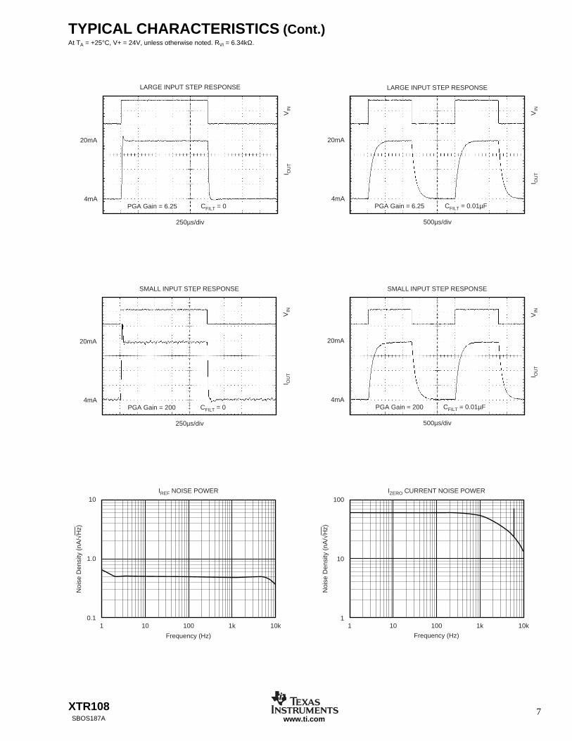
TYPICAL CHARACTERISTICS (Cont.)At TA = +25°C, V+ = 24V, unless otherwise noted. RVI = 6.34kΩ.
LARGE INPUT STEP RESPONSE
250µs/div
PGA Gain = 6.25 CFILT = 0
VIN
I OU
T
20mA
4mA
LARGE INPUT STEP RESPONSE
500µs/div
PGA Gain = 6.25 CFILT = 0.01µF
VIN
I OU
T
20mA
4mA
SMALL INPUT STEP RESPONSE
250µs/div
VIN
I OU
T
20mA
4mAPGA Gain = 200 CFILT = 0
SMALL INPUT STEP RESPONSE
VIN
I OU
T
20mA
4mA
500µs/div
PGA Gain = 200 CFILT = 0.01µF
IREF NOISE POWER
Frequency (Hz)
10 100 1k 10k1
Noi
se D
ensi
ty (
nA/√
Hz)
10
1.0
0.1
IZERO CURRENT NOISE POWER
Frequency (Hz)
10 100 1k 10k1
Noi
se D
ensi
ty (
nA/√
Hz)
100
10
1
XTR1088SBOS187Awww.ti.com
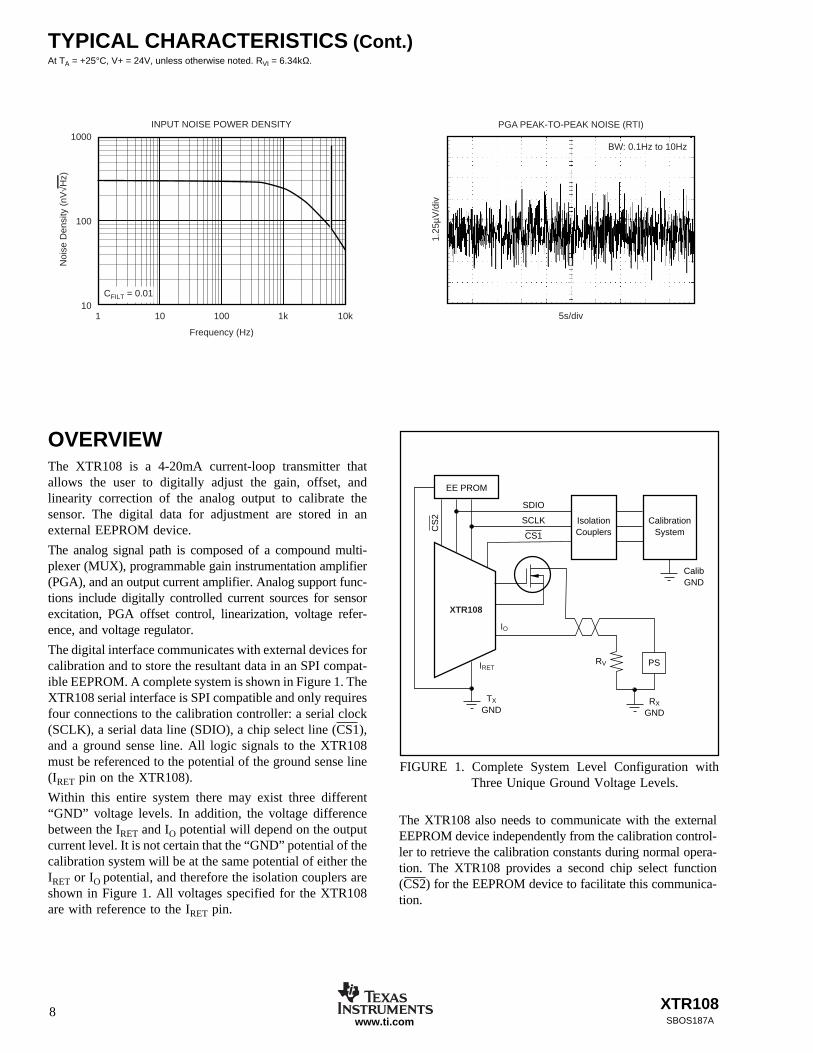
TYPICAL CHARACTERISTICS (Cont.)At TA = +25°C, V+ = 24V, unless otherwise noted. RVI = 6.34kΩ.
INPUT NOISE POWER DENSITY
10 100 1k 10k1
Frequency (Hz)
Noi
se D
ensi
ty (
nV√H
z)
1000
100
10CFILT = 0.01
PGA PEAK-TO-PEAK NOISE (RTI)
5s/div
1.25
µV/d
iv
BW: 0.1Hz to 10Hz
OVERVIEWThe XTR108 is a 4-20mA current-loop transmitter thatallows the user to digitally adjust the gain, offset, andlinearity correction of the analog output to calibrate thesensor. The digital data for adjustment are stored in anexternal EEPROM device.
The analog signal path is composed of a compound multi-plexer (MUX), programmable gain instrumentation amplifier(PGA), and an output current amplifier. Analog support func-tions include digitally controlled current sources for sensorexcitation, PGA offset control, linearization, voltage refer-ence, and voltage regulator.
The digital interface communicates with external devices forcalibration and to store the resultant data in an SPI compat-ible EEPROM. A complete system is shown in Figure 1. TheXTR108 serial interface is SPI compatible and only requiresfour connections to the calibration controller: a serial clock(SCLK), a serial data line (SDIO), a chip select line (CS1),and a ground sense line. All logic signals to the XTR108must be referenced to the potential of the ground sense line(IRET pin on the XTR108).
Within this entire system there may exist three different“GND” voltage levels. In addition, the voltage differencebetween the IRET and IO potential will depend on the outputcurrent level. It is not certain that the “GND” potential of thecalibration system will be at the same potential of either theIRET or IO potential, and therefore the isolation couplers areshown in Figure 1. All voltages specified for the XTR108are with reference to the IRET pin.
EE PROM
SDIO
CS
2 SCLK
CS1
IsolationCouplers
IO
IRET
XTR108
RV
RX
GND
PS
CalibrationSystem
CalibGND
TX
GND
FIGURE 1. Complete System Level Configuration withThree Unique Ground Voltage Levels.
The XTR108 also needs to communicate with the externalEEPROM device independently from the calibration control-ler to retrieve the calibration constants during normal opera-tion. The XTR108 provides a second chip select function(CS2) for the EEPROM device to facilitate this communica-tion.
XTR108 9SBOS187A www.ti.com
THEORY OF OPERATIONREFERENCE
The XTR108 has an on-board precision bandgap voltagereference with output at pin 21 (REFOUT). The value of thereference is factory-trimmed to 1.193V, with a typical tem-perature drift of 5ppm/°C. Pins 21 (REFOUT) and 20 (REFIN)must be connected together to use the internal reference.
External circuitry, such as a voltage excited sensor or anAnalog-to-Digital Converter (ADC), can be connected to theREFOUT pin. The unbuffered REFOUT is capable of sourcingcurrent but not sinking.
If the application necessitates, an external reference can beconnected to the XTR108 REFIN pin, as long as the referencedoes not exceed 1.4V. The REFIN pin has a high inputimpedance with the input current not exceeding a fewnanoamps.
INPUT MULTIPLEXER
The XTR108 input multiplexer is a full 6 by (2+2) cross-point switch. The current references and PGA inputs can beindependently connected to any of the six external pins,including simultaneous connections to the same pin. Thisallows a great flexibility in the sensor excitation and inputconfiguration. The input pins must not be driven below theIRET potential or above VS.
See Figure 2 for an RTD sensor connected to pin VIN0 withboth IREF supplied and PGA VIN+ sensed at that pin. Theother five input pins are used for a bank of RZ resistors thatcan be selected during the calibration process for a particularmeasurement range.
PROGRAMMABLE GAININSTRUMENTATION AMPLIFIER
The programmable gain instrumentation amplifier has sevenvoltage-gain settings in binary steps from 6.25V/V to 400V/V.The input common-mode range of the PGA is 0.2V to 3.5Vabove the IRET potential.
Normally, in the application for 4-20mA transmitters, thePGA output voltage range should be set to VZERO = 0.5V andVFS = 2.5V. Connecting a resistor (RVI = 6.34kΩ) betweenpin 9 (VO) and pin 10 (IIN) converts this voltage to the signalfor the output amplifier that produces a 4-20mA scalecurrent output. In this mode, the PGA voltage gain convertsto an overall transconductance in the range of 50mA/V to3200mA/V (approximately). Table I shows the gain totransconductance relationship.
If over-scale and under-scale limiting is disabled, the PGAcan be used with rail-to-rail voltage output, for example, inapplications that require a 0.5V to 4.5V voltage scale.
The PGA uses advanced auto-zero circuit techniques to achievehigh DC precision, and reduce mismatches and errors withinthe chip such as input offset, offset temperature drift, and low-frequency noise (see the input noise typical characteristic).
The basic clock frequency of the auto-zero loop is about6.5kHz. Due to the switching nature of the auto-zero circuit,the output of the PGA can have a noticeable clock feed-through ripple in higher gains. This noise can be reduced bythe addition of a 0.01µF capacitor between pin 7 (CFILTER)and the local ground, pin 12 (IRET). This creates a one-polelow-pass filter with –3dB frequency at about 1.5kHz. Ifwider bandwidth or faster settling time is needed, the CFILTERcan be reduced or eliminated at the expense of higher glitchamplitude at the output. Please refer to the typical stepresponse traces for settling time comparisons.
ZERO DACS
Two output-referred, 8-bit Digital-to-Analog Converters(DACs) (coarse and fine with a pedestal) set the zero level ofthe PGA output. They allow setting a desired zero-scaleoutput level and compensate the initial offset at the PGA inputdue to the sensor and resistor mismatches, sensor non-ideali-ties, etc. Both coarse and fine DACs are bidirectional andallow the output level to be set above or below a presetpedestal.
Output signals of the DACs, IZ COARSE and IZ FINE, aresummed with the pedestal, IZ PROGRAM. Each of the DACshas 8-bit resolution (256 steps) with 4-bit overlap betweenthe coarse and fine DACs. This means that one LSB of thecoarse DAC is equal to 16 fine LSBs, and the full-scalerange of the fine DAC is equal to 16 coarse LSBs. Thiseffectively produces 12-bit adjustment resolution.
This overlap allows the user to set pre-calculated valuesbefore the calibration, using the coarse DAC only and adjustthe zero output level with the fine DAC during the calibra-tion process see Table II for the equations for calculating thevalue of the output when zero differential voltage is appliedat the PGA input. For the adjustment range, LSB sizes, andlinearity values of the Zero DACs, please refer to theelectrical characteristics table.
Note that a DAC can be set to a value that produces anoutput below the under-scale level. In this case, the under-scale limit will prevent the output from getting to the desiredvalue. The value of the minimum scale should not be set solow that the PGA voltage output, VO, goes below its speci-fied range of 0.2V from IRET.
ADJUSTABLE OVER-SCALE ANDUNDER-SCALE LIMITING CIRCUIT
The XTR108 incorporates circuitry to set adjustable limits atthe output in cases when the sensor signal goes above orbelow its range. There are 16 levels for over-scale limitadjustment (4-bit DAC) and 8 levels for the under-scale (3-bitDAC).
VOLTAGE GAIN 6.25 12.5 25 50 100 200 400V/V
OUTPUT TRANSCONDUCTANCE 49 99 197 394 789 1577 3155mA/V
FULL-SCALE DIFFERENTIAL VIN 320 160 80 40 20 10 5mV
TABLE I. PGA Gain, Corresponding Loop Transductanceand Input Full-Scale Differential Voltage.
XTR10810SBOS187Awww.ti.com
FIGURE 2. XTR108 Internal Block Diagram.
4-20
mA
Vol
tage
Ref
eren
ce
Sub
-Reg
ulat
orD
river
Line
ariz
atio
nC
ircui
t
Multiplexer
SD
IOS
CLK
CS
2C
S1
V/I-
0
V/I-
1
V/I-
2
V/I-
3
V/I-
4
V/I-
5
RT
D
RZ
1R
Z2
RZ
3R
Z4
RZ
5
CF
ILT
0.01
µFR
CM
15.8
kΩ12
.1kΩ
RS
ET
RLI
N
RV
I6.
34kΩ
VO
UT
I IN
PG
A
OP
A +
INO
PA
–IN
OP
A O
UT
RE
FIN
RE
FO
UT
Σ
VG
ate
VS
I O
I RE
T
I RE
F
DA
C
I LIN
DA
C
Zer
oD
AC
SP
I and
Con
trol
Circ
uits
OS
C
RLO
AD
+ –Lo
opS
uppl
y
XT
R10
8
CG
AT
E
CR
EG
CLO
OP
Out
put
Cur
rent
Am
plifi
er
12
2.5k
Ω51
Ω
XTR108 11SBOS187A www.ti.com
The circuit is designed for compliance with NAMUR NE43recommendation for sensor interfaces. The limit levels arelisted in Tables VII and VIII. Because of the large step sizes,units that use this feature should be checked if the value iscritical. The under-scale limit circuit will override the ZeroDAC level if it is set lower and there is not enough sensoroffset at the PGA input.
It may be necessary to disable limiting if the XTR108 is usedin applications other than a 4-20mA transmitter, where thePGA output is between 0.5V and 4.5V.
SENSOR FAULT DETECTION CIRCUIT
To detect sensor burnout and/or short, a set of four compara-tors is connected to the inputs of the PGA. If any of theinputs are taken outside of the PGA’s common-mode range,the corresponding comparator sets a sensor fault flag thatcauses the PGA output to go either to the upper or lowererror limit. The state of the fault condition can be read in thedigital form from register 3. The direction of the analogoutput is set according to the “Alarm Configuration Regis-ter” (see Table X). The level of the output is produced asfollows: if the over-scale/under-scale limiting is enabled, theerror levels are: over-scale limit +2LSBs of the over-scaleDAC, about 1mA referred to IOUT or 0.125V referred to VO,of under-scale limit –2LSBs of the under-scale DAC, about0.4mA referred to IOUT or 0.05V referred to VO. If the over-scale/under-scale limiting is disabled, the PGA output volt-age will go to within 150mV of either positive or negativesupply (VS or IRET), depending on the alarm configurationbit corresponding to the error condition.
OUTPUT CURRENT AMPLIFIER + RVI RESISTOR
To produce the 4-20mA output, the XTR108 uses a currentamplifier with a fixed gain of 50A/A. The voltage from thePGA is converted to current by the external resistor, RVI. PinIRET, the common potential of the circuit (substrate and localground), is connected to the output and inverting input of theamplifier. This allows collecting all external and internalsupply currents, sensor return current, and leakage currentsfrom the different parts of the system and accounting forthem in the output current. The current from RVI flows intothe pin IIN that is connected to the noninverting input andtherefore, is at ground potential as well. The ratio of two
VOLTAGE REFERRED TO VO PINWITH RESPECT TO IRET CURRENT REFERRED TO IOUT PIN
OVERALL VZERO = VZ PROGRAM + VZ COARSE + VZ FINE IZERO = IZ PROGRAM + IZ COARSE + IZ FINE
PROGRAM VV
Z PROGRAMREF=
3 5
8
. IV
RZ PROGRAMREF
VI=
175
8
COARSE DAC VV N
Z COARSEREF= •80 4
13 IV
R
NZ COARSE
REF
VI= •
5
8 413
FINE DAC VV N
Z FINEREF= •80 64
12 IV
R
NZ FINE
REF
VI= •
5
8 6412
NOTE: N13 and N12 are assigned decimal values of registers 13 and 12, respectively.
TABLE II. Equations for Calculating Zero Output.
REFERENCE CURRENT
OVERALL IREF1, 2 = IREF PROGRAM + IREF COARSE + IREF FINE
PROGRAM IV
RREF PROGRAMREF
SET
=5
COARSE DAC IV
R
NREF COARSE
REF
SET
= • 11
64
FINE DAC IV
R
NREF FINE
REF
SET
= • 10
1024
NOTE: N11 and N10 are the decimal values of registers 11 and 10,respectively.
TABLE III. Equations for Calculating the Values of EachReference Current.
matched internal resistors determines a current gain of thisblock. Note that the IOUT pin is always biased below thesubstrate potential.
EXCITATION CURRENT DACS AND RSET RESISTOR
Two matched adjustable reference current sources are avail-able for sensor excitation. The defining equations are givenin Table III. Both current sources are controlled simulta-neously by the coarse and fine DACs with a pedestal.
The external resistor RSET is used to convert the REF voltageinto the reference current for the sensor excitation DACs.The total current output of the DACs is split, producing tworeferences: IREF1 and IREF2. Both of the current referencesmatch very closely over the full adjustment range withoutmismatched differential steps. Both current reference out-puts must be within the compliance range, i.e.: one referencecannot be floated since it will change the value of the othercurrent source.
The recommended value of RSET is 12.1kΩ for use with100Ω RTD sensors. This generates IREF1, 2 = 492µA currentswhen both coarse and fine DACs are set to zero. The valueof the RSET resistor can be increased if lower referencecurrents are required, i.e.: for 1000Ω RTD or a bridgesensor.
Similar to the Zero DACs, the outputs of the fine and coarseDAC are summed together with the pedestal IREF PROGRAM.Each of the excitation DACs has 8-bit resolution (256 steps)with 4-bit overlap between the coarse and the fine. This
XTR10812SBOS187Awww.ti.com
means that one LSB of the coarse DAC is equal to 16 fineLSBs, and the full-scale range of the fine DAC is equal to 16coarse LSBs. This effectively produces 12-bit adjustmentresolution. This allows the user to set pre-calculated valuesbefore the calibration, using the coarse DAC only and adjustthe reference current output level with the fine DAC duringthe calibration process.
LINEARIZATION CIRCUIT AND RLIN RESISTOR
The XTR108 incorporates circuitry for correcting a second-order sensor nonlinearity. A current proportional to thevoltage at the input of the PGA is added to the sensorexcitation. The RLIN resistor is used to convert this voltageinto current. By appropriately scaling this current using thelinearization DAC, parabolic sensor nonlinearity can beimproved by up to a 40:1 ratio, as shown in Figure 3. Thelinearization coefficient (ratio of the reference current changeto the input voltage) is expressed in µA/mV as follows:
GI
V
N
RLINREF
IN LIN
= ••
∆ 14
16
where N14 is the decimal value from register 14.
The recommended value of the resistor is 15.8kΩ, for usewith 100Ω RTD sensors. This value produces a full-scalelinearization coefficient of about 1mA/V. Please see thesection below on using the XTR108 with an RTD tempera-ture sensor. If the sensor excitation is scaled down byincreasing the value of RSET, the value of RLIN should bescaled proportionally.
SUB-REGULATOR WITH EXTERNAL MOSFET
The XTR108 is manufactured using a low-voltage CMOSprocess with maximum supply voltage limited to 5.5V. Forapplications in a 4-20mA current loop, a special sub-regulatorcircuit is incorporated in the device that requires an external
n-channel depletion-mode MOS transistor and three capaci-tors, see Figure 2.
A number of third-party suppliers make n-channel deple-tion-mode MOSFETs. A list of devices tested by TexasInstruments, Inc. is shown in Table IV with the capacitorvalues recommended for those devices.
The capacitors CLOOP (0.01µF), CREG (2.2µF), and CGATEare required for the regulator loop stability and supplybypass. They should be placed in close proximity to theXTR108 on the PCB. An additional 1µF capacitor may beused to bypass the supply of an EEPROM chip.
If a MOSFET other than those listed in Table IV is used, thevalue of CGATE should be adjusted such that there is noovershoot of VS during power-up and supply glitches. AnyVS overshoot above 7.5V may damage the XTR108 ordeteriorate its performance.
LOOP VOLTAGE
The XTR108 transmitter minimum loop voltage can some-what be effected by the choice of the external MOSFET. Thedevices are tested to 7.5V compliance with Supertex DN2540;choosing other MOSFETs can change this value slightly.
The maximum loop voltage is limited by the power dissipa-tion on the MOSFET as well as its breakdown voltage.Possible ambient temperatures and the power dissipationshould be taken into account when selecting the MOSFETpackage. The external MOSFET can dissipate a consider-able amount of power when running at high loop supply. Forexample, if VLOOP = 24V and IOUT = 20mA, the DC powerdissipated by the MOSFET is:
PMOSFET = IOUT (VLOOP – VS) = 380mΩFor a SOT-89 package soldered on an FR5 board, this willcause a 30°C rise in the temperature. The power dissipationgets significantly higher when the circuit is driven into anover-scale condition. Therefore, special attention should bepaid to removing the heat from the MOSFET, especiallywith small-footprint packages such as SOT-89 and TO-92.Please follow manufacturer’s recommendations about thepackage thermal characteristics and board mounting.
UNCOMMITTED OP AMP
For added flexibility in various applications, the XTR108has an on-chip uncommitted operational amplifier. The opamp has rail-to-rail output range. The input range extends toIRET potential.
FIGURE 3. Pt100 Nonlinearity Correction Using the XTR108.
–200°CProcess Temperature (°C)
+850°C
5
4
3
2
1
0
–1
UncorrectedRTD Nonlinearity
CorrectedNonlinearity
Non
linea
rity
(%)
MANUFACTURER MOSFET MODEL CGATE VALUE
Supertex DN2535, DN2540 220pFDN3535, DN3525 1000pF
Siliconix ND2012, ND2020 220pF
Infineon BSP149 1000pF
TABLE IV. Recommended Gate Capacitor Values For Se-lected MOSFETs.
XTR108 13SBOS187A www.ti.com
The uncommitted amplifier can be used for a variety ofpurposes, such as voltage sensor excitation, buffering theREFOUT pin, four-wire RTD connection, or sensing thebridge voltage for temperature compensation.
POWER-GOOD/POWER-ON RESET
In case of a supply brownout condition or short interruption,the XTR108 power-good detection circuit will initiate a chipreset that will cause all registers to be reset to 0’s and a cycleof EEPROM read to begin. The circuit generates a reset ifVS droops below 1.5V and then recovers up to the normallevel.
USING THE XTR108 IN VOLTAGE OUTPUT MODE
The XTR108 can be used not only in 4-20mA current loops,but also as a low-power, single-supply, “smart” sensor-condi-tioning chip with voltage output. In this mode, the pin IRETmust be grounded. The sub-regulator with an external MOSFETmay or may not be used. If the circuit is powered externally,the supply voltage must be in the range of 5V to ±0.5V.
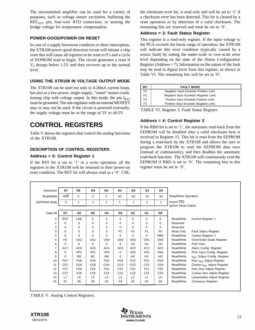
CONTROL REGISTERSTable V shows the registers that control the analog functionsof the XTR108.
DESCRIPTION OF CONTROL REGISTERS
Address = 0: Control Register 1
If the RST bit is set to ‘1’ in a write operation, all theregisters in the XTR108 will be returned to their power-onreset condition. The RST bit will always read as a ‘0’. CSE,
the checksum error bit, is read only and will be set to ‘1’ ifa checksum error has been detected. This bit is cleared by areset operation or by detection of a valid checksum. Theremaining bits are reserved and must be set to ‘0’.
Address = 3: Fault Status Register
This register is a read-only register. If the input voltage tothe PGA exceeds the linear range of operation, the XTR108will indicate this error condition (typically caused by asensor fault) by setting the under-scale or over-scale errorlevel depending on the state of the Alarm ConfigurationRegister (Address = 7). Information on the nature of the faultmay be read in digital form from this register, as shown inTable VI. The remaining bits will be set to ‘0’.
Address = 4: Control Register 2
If the RBD bit is set to ‘1’, the automatic read-back from theEEPROM will be disabled after a valid checksum byte isreceived in Register 15. This bit is read from the EEPROMduring a read-back by the XTR108 and allows the user toprogram the XTR108 to read the EEPROM data once(instead of continuously), and then disables the automaticread-back function. The XTR108 will continuously read theEEPROM if RBD is set to ‘0’. The remaining bits in thisregister must be set to ‘0’.
TABLE V. Analog Control Registers.
Instruction D7 D6 D5 D4 D3 D2 D1 D0
Read/Write R/W 0 0 0 A3 A2 A1 A0
EEPROM Mode 0 1 1 1 1 1 1 1
D7 D6 D5 D4 D3 D2 D1 D0
0 RST CSE 0 0 0 0 0 0 Read/Write Control Register 11 0 0 0 0 0 0 0 0 Reserved2 0 0 0 0 0 0 0 0 Reserved3 0 0 0 0 F3 F2 F1 F0 Read Only Fault Status Register4 0 0 0 0 0 0 0 RBD Read/Write Control Register 25 FD US2 US1 US0 OS3 OS2 OS1 OS0 Read/Write Over/Under-Scale Register6 0 0 0 0 0 G2 G1 G0 Read/Write PGA Gain7 AC7 AC6 AC5 AC4 AC3 AC2 AC1 AC0 Read/Write Alarm Config. Register8 0 VP2 VP1 VP0 0 VN2 VN1 VN0 Read/Write PGA Input Config. Register9 0 IB2 IB1 IB0 0 IA2 IA1 IA0 Read/Write IREF Output Config. Register
10 FG7 FG6 FG5 FG4 FG3 FG2 FG1 FG0 Read/Write Fine IREF Adjust Register11 CG7 CG6 CG5 CG4 CG3 CG2 CG1 CG0 Read/Write Coarse IREF Adjust Register12 FZ7 FZ6 FZ5 FZ4 FZ3 FZ2 FZ1 FZ0 Read/Write Fine Zero Adjust Register13 CZ7 CZ6 CZ5 CZ4 CZ3 CZ2 CZ1 CZ0 Read/Write Coarse Zero Adjust Register14 L7 L6 L5 L4 L3 L2 L1 L0 Read/Write Linearization Adjust Register15 S7 S6 S5 S4 S3 S2 S1 S0 Read/Write Checksum Register
Read/Write Operation
Data Bit
Assert CS2Ignore Serial Data/A
BIT FAULT MODEF0 Negative Input Exceeds Positive Limit.F1 Negative Input Exceeds Negative Limit.F2 Positive Input Exceeds Positive Limit.F3 Positive Input Exceeds Negative Limit.
TABLE VI. Register 3, Fault Status Register.
XTR10814SBOS187Awww.ti.com
Address = 5: Over- and Under-Scale Register
This register sets the magnitude of the over-scale currentlimit and the magnitude of the under-scale current limit. Thethreshold level, as shown in Table VII and VIII, is thenormal analog (no error condition) output limit. If an inputvoltage to the PGA exceeds the linear operation range, theoutput will be programmed to either the over-scale errorlevel or the under-scale error level. The over-scale errorlevel is 10mA greater than the over-scale threshold level.The under-scale error level is 0.4mA less than the under-scale threshold level. The FD bit will disable the over-scaleand under-scale limiting function as well as the PGA faultindication error levels.
Address = 6: PGA Gain Register
This register sets the gain of the programmable-gain ampli-fier. The unused bits must always be set to ‘0’. The gain stepto register content is given in Table IX.
Address = 7: Alarm Configuration Register
This register configures whether the XTR108 will go over-scale or under-scale for various detected fault conditions atthe input of the PGA. Table X defines each of the bits.
If a bit corresponding to the particular error is set to ‘1’, theoutput will go over-scale when it occurs and if a bit corre-sponding to the particular error is set to ‘0’, the output willgo under-scale.
Address = 8: PGA Input Configuration Register
This register connects the inputs of the PGA to the variousmultiplexed input pins. Tables XI and XII show the relation-ship between register, contents, and PGA inputs.
Address = 9: IREF Output Configuration Register
This register connects the reference currents to the variousmultiplexed input pins. IREF connection codes are given inTable XIII.
Address = 10: Fine IREF Adjust Register
This register sets the code to the 8-bit Fine DAC that adjuststhe magnitude of both reference currents. The DAC outputvalue has a bipolar range (for each reference current) andcan be calculated using the equations in Table III.
IO UNDER-SCALEVO UNDER-SCALE THRESHOLD
US2 US1 US0 THRESHOLD RVI = 6.34kΩ
0 0 0 450mV 3.55mA0 0 1 425mV 3.35mA0 1 0 400mV 3.15mA0 1 1 375mV 2.96mA1 0 0 350mV 2.76mA1 0 1 325mV 2.56mA1 1 0 300mV 2.37mA1 1 1 275mV 2.17mA
TABLE VIII. Register 5, Under-Scale Threshold.
IO OVER-SCALEVO OVER-SCALE THRESHOLD
OS3 OS2 OS1 OS0 THRESHOLD RVI = 6.34kΩ
0 0 0 0 2.625V 20.7mA0 0 0 1 2.6875V 21.2mA0 0 1 0 2.75V 21.7mA0 0 1 1 2.8125V 22.2mA0 1 0 0 2.875V 22.7mA0 1 0 1 2.9375V 23.2mA0 1 1 0 3.0V 23.7mA0 1 1 1 3.0625V 24.2mA1 0 0 0 3.125V 24.6mA1 0 0 1 3.1875V 25.1mA1 0 1 0 3.25V 25.6mA1 0 1 1 3.3125V 26.1mA1 1 0 0 3.375V 26.6mA1 1 0 1 3.4375V 27.1mA1 1 1 0 3.5V 27.6mA1 1 1 1 3.5625V 28.1mA
TABLE VII. Register 5, Over-Scale Threshold.
SIGNAL PATHPGA TRANSCONDUCTANCE
G2 G1 G0 VOLTAGE GAIN RVI = 6.34kΩ
0 0 0 6.25V/V 49mA/V0 0 1 12.5V/V 99mA/V0 1 0 25V/V 197mA/V0 1 1 50V/V 394mA/V1 0 0 100V/V 789mA/V1 0 1 200V/V 1577mA/V1 1 0 400V/V 3155mA/V1 1 1 Reserved
TABLE IX. Register 6, PGA Gains.
BIT AC AC AC AC AC AC AC AC
# 7 6 5 4 3 2 1 0VINN h l l h n n l hVINP l h l h l h n n
NOTES: ‘h’ = input exceeds positive common-mode range, ‘l’ = input exceedsnegative common-mode range, and ‘n’ = input pin is within the CM range.
TABLE X. Register 7, Alarm Configuration Register.
VP2 VP1 VP0 PGA POSITIVE INPUT
0 0 0 PGA VIN+ Connected to V/ I-00 0 1 PGA VIN+ Connected to V/ I-10 1 0 PGA VIN+ Connected to V/ I-20 1 1 PGA VIN+ Connected to V/ I-31 0 0 PGA VIN+ Connected to V/ I-41 0 1 PGA VIN+ Connected to V/ I-51 1 0 Reserved1 1 1 Reserved
TABLE XI. Register 8, PGA Positive Input Selection.
VN2 VN1 VN0 PGA NEGATIVE INPUT
0 0 0 PGA VIN– Connected to V/ I-00 0 1 PGA VIN– Connected to V/ I-10 1 0 PGA VIN– Connected to V/ I-20 1 1 PGA VIN– Connected to V/ I-31 0 0 PGA VIN– Connected to V/ I-41 0 1 PGA VIN– Connected to V/ I-51 1 0 Reserved1 1 1 Reserved
TABLE XII. Register 8, PGA Negative Input Selection.
XTR108 15SBOS187A www.ti.com
Address = 11: Coarse IREF Adjust Register
This register sets the code to the 8-bit coarse DAC that adjuststhe magnitude of both reference currents. The nominal valuefor the reference current (both Coarse and Fine adjust set to ‘0’)is IPROGRAM • 5. See Table III for formulas.
Address = 12: Fine Zero-Adjust Register
This register sets the code to the 8-bit Fine DAC that adjuststhe magnitude of the zero output currents. Equations aregiven in Table II. Negative numbers are in Binary Two’sComplement.
Address = 13: Coarse Zero-Adjust Register
This register sets the code to the 8-bit Coarse DAC thatadjusts the magnitude of zero-output current. See Table IIfor equations. Negative numbers are given in Binary Two’sComplement.
Address = 14: Linearization Adjust Register
This register sets the code to the 8-bit DAC that adjusts themagnitude of the linearization feedback current. Value isunipolar to 255.
Address = 15: Checksum Register
This register contains the checksum byte that is used tovalidate the data read from the EEPROM. If a write occursto this register, and the checksum is invalid, an error condi-tion will set (CSE = ‘1’). If the checksum is valid, the errorcondition will be cleared (CSE = ‘0’).
If a checksum error is detected, the XTR108 will programitself to the lowest under-scale error level.
SERIAL INTERFACEPROTOCOL
The XTR108 has an SPI-compatible serial interface. Thedata is transmitted MSB first in 8-bit bytes. The first byte isan instruction byte in which the first bit is a read/write flag(‘0’ = write, ‘1’ = read), the lowest four bits are the registeraddress and the remaining three bits are set to zero. Thesecond, and all successive bytes, are data. During a writeoperation, the successive data bytes are written to successive
registers within the XTR108. The address is automaticallyincremented at the completion of each byte. The SDIO lineis always an input during a write operation. During a readoperation, the SDIO line becomes an output during thesecond and successive bytes. As in the case of a writeoperation, the address is automatically incremented at thecompletion of each byte. Each communication transaction isterminated when CS1 is de-asserted. The CS2 line remainsde-asserted during read and write operations.
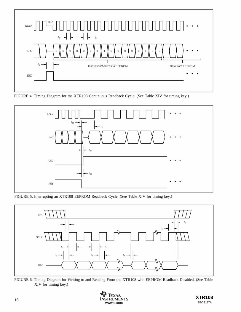
The calibration controller also needs to be able to read fromand write to the external EEPROM device. This is accom-plished by sending a special instruction code (0x7F) to theXTR108. At the completion of this instruction byte, theXTR108 will assert the CS2 line to select the EEPROMdevice and ignore all data on the SDIO line until CS1 is de-asserted and reasserted. The CS2 line will also be de-asserted when CS1 is de-asserted. This allows the calibra-tion controller to communicate with the EEPROM devicedirectly. The calibration controller then has control over thetiming required to write data to the EEPROM device.In normal operation, the XTR108 reads data from the EEPROMdevice to retrieve calibration coefficients. This is accom-plished by the read-back controller on the XTR108. The read-back controller is clocked by an on-chip oscillator and pro-vides stimulus to the EEPROM device over the SCLK, SDIO,and CS2 lines to perform the read operation, while simulta-neously providing stimulus to the serial interface controller inthe XTR108. The read-back controller defaults to being activewhen the XTR108 is powered on and will be continuouslyactive unless disabled. (It will start a new read operation assoon as the previous operation is completed, see Figure 4.) Acontrol bit (RBD) is provided to allow the XTR108 to read theEEPROM once and then stop.
The read-back controller will abort a read-back operationwhen the CS1 line is asserted. The calibration controllermust wait at least 40µs after setting the CS1 line LOWbefore the first rising edge of SCLK occurs.
For an external controller to write directly to the XTR108(sensor calibration operation) or load data into the EEPROM,it is necessary to interrupt the default read-back mode. Forboth of these modes, the SCLK direction must be reversed.See Figure 5 for the timing of this operation. First, the SCLKline must be pulled LOW for at least 20ns (t10). Then CS1is set LOW. The XTR108 will set DIO to a tri-state within20ns (t13) and CS2 HIGH within 50ns (t12). After a delay ofat least 40ns (t11), the external system will start communica-tion with a rising edge on SCLK.As long as CS1 is held LOW, the external system can write tothe EEPROM. See Figure 7 for this timing. Releasing CS1will allow the XTR108 to resume in the read-back mode.
For interactive calibration operations, the first command tothe XTR108 should set bit 0, Register 4 (RBD). This willdisable the read-back mode. It will be possible to write to thevarious registers and cycle CS1. If RBD is not set, then assoon as CS1 is released, the XTR108 will read the EEPROMcontents which will overwrite the data just loaded. Figure 6shows read and write timing.
IA2 IA1 IA0 IREF CONNECTION
0 0 0 IREF1 Connected to V/ I-00 0 1 IREF1 Connected to V/ I-10 1 0 IREF1 Connected to V/ I-20 1 1 IREF1 Connected to V/ I-31 0 0 IREF1 Connected to V/ I-41 0 1 IREF1 Connected to V/ I-51 1 0 Reserved1 1 1 Reserved
IB2 IB1 IB0 IREF CONNECTION
0 0 0 IREF2 Connected to V/ I-00 0 1 IREF2 Connected to V/ I-10 1 0 IREF2 Connected to V/ I-20 1 1 IREF2 Connected to V/ I-31 0 0 IREF2 Connected to V/ I-41 0 1 IREF2 Connected to V/ I-51 1 0 Reserved1 1 1 Reserved
TABLE XIII. Register 9, IREF Output Configuration.
XTR10816SBOS187Awww.ti.com
FIGURE 5. Interrupting an XTR108 EEPROM Readback Cycle. (See Table XIV for timing key.)
FIGURE 4. Timing Diagram for the XTR108 Continuous Readback Cycle. (See Table XIV for timing key.)
FIGURE 6. Timing Diagram for Writing to and Reading From the XTR108 with EEPROM Readback Disabled. (See TableXIV for timing key.)
Instruction/Address to EEPROM Data from EEPROM
CS2
SCLK
t8 t8
t9
DIO 0 0 0 0 0 0 1 1 0 0 0 0 0 1 0 0
Hi-Z
t10
CS2
SCLK
t11
t13
t12
DIO
CS1
CS1
SCLK
t1
t2 t2
t3 t4 t6
t5
t7
DIO
XTR108 17SBOS187A www.ti.com
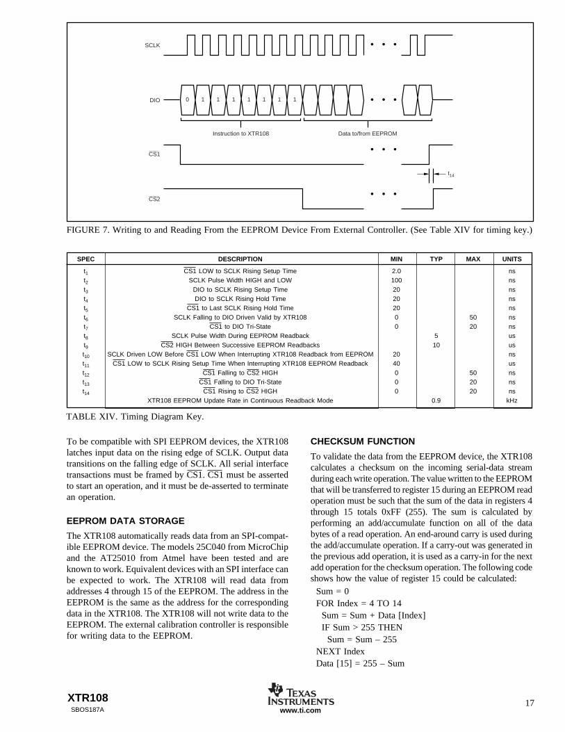
FIGURE 7. Writing to and Reading From the EEPROM Device From External Controller. (See Table XIV for timing key.)
Instruction to XTR108 Data to/from EEPROM
CS2
SCLK
t14
DIO 0 1 1 1 1 1 1 1
CS1
SPEC DESCRIPTION MIN TYP MAX UNITS
t1 CS1 LOW to SCLK Rising Setup Time 2.0 nst2 SCLK Pulse Width HIGH and LOW 100 nst3 DIO to SCLK Rising Setup Time 20 nst4 DIO to SCLK Rising Hold Time 20 nst5 CS1 to Last SCLK Rising Hold Time 20 nst6 SCLK Falling to DIO Driven Valid by XTR108 0 50 nst7 CS1 to DIO Tri-State 0 20 nst8 SCLK Pulse Width During EEPROM Readback 5 ust9 CS2 HIGH Between Successive EEPROM Readbacks 10 ust10 SCLK Driven LOW Before CS1 LOW When Interrupting XTR108 Readback from EEPROM 20 nst11 CS1 LOW to SCLK Rising Setup Time When Interrupting XTR108 EEPROM Readback 40 ust12 CS1 Falling to CS2 HIGH 0 50 nst13 CS1 Falling to DIO Tri-State 0 20 nst14 CS1 Rising to CS2 HIGH 0 20 ns
XTR108 EEPROM Update Rate in Continuous Readback Mode 0.9 kHz
TABLE XIV. Timing Diagram Key.
To be compatible with SPI EEPROM devices, the XTR108latches input data on the rising edge of SCLK. Output datatransitions on the falling edge of SCLK. All serial interfacetransactions must be framed by CS1. CS1 must be assertedto start an operation, and it must be de-asserted to terminatean operation.
EEPROM DATA STORAGE
The XTR108 automatically reads data from an SPI-compat-ible EEPROM device. The models 25C040 from MicroChipand the AT25010 from Atmel have been tested and areknown to work. Equivalent devices with an SPI interface canbe expected to work. The XTR108 will read data fromaddresses 4 through 15 of the EEPROM. The address in theEEPROM is the same as the address for the correspondingdata in the XTR108. The XTR108 will not write data to theEEPROM. The external calibration controller is responsiblefor writing data to the EEPROM.
CHECKSUM FUNCTION
To validate the data from the EEPROM device, the XTR108calculates a checksum on the incoming serial-data streamduring each write operation. The value written to the EEPROMthat will be transferred to register 15 during an EEPROM readoperation must be such that the sum of the data in registers 4through 15 totals 0xFF (255). The sum is calculated byperforming an add/accumulate function on all of the databytes of a read operation. An end-around carry is used duringthe add/accumulate operation. If a carry-out was generated inthe previous add operation, it is used as a carry-in for the nextadd operation for the checksum operation. The following codeshows how the value of register 15 could be calculated:
Sum = 0FOR Index = 4 TO 14
Sum = Sum + Data [Index]IF Sum > 255 THEN
Sum = Sum – 255NEXT IndexData [15] = 255 – Sum
XTR10818SBOS187Awww.ti.com
For a test or calibration operation, it may be necessary towrite to a few select registers. This may be accomplishedwithout writing to register 15. To accomplish this, write tothe necessary registers and release CS1. There is no need toupdate register 15.
If the command is to disable the automatic read-back func-tion by setting the RDB bit in register 4, it is necessary torewrite the entire register set data with a correct checksumvalue in register 15. The automatic read-back mode will bedisabled upon successful checksum operation.
The checksum error flag is also cleared when the XTR108is reset (i.e.: at power ON). Write operations that do notwrite to the checksum register will have no effect on thechecksum error flag. By locating the checksum register afterthe last configuration register and including the checksumregister in the EEPROM read operation, the data is validatedby the checksum function.
EEPROM DATA SECURITYSince the data in the EEPROM directly affects the analogoutput of the XTR108, the data in the EEPROM needs to besecure from accidental write operations. SPI EEPROM de-vices have a write-protect function on one of the pins. Anadditional connection to the calibration controller would berequired if the write-protect pin is used to prevent accidentalwrite operations. SPI EEPROM devices require a specialwrite enable instruction to be executed to write data to theEEPROM. It is unlikely that this would accidentally bewritten to the EEPROM device and then be followed by avalid write operation. Further security can be obtained byusing an SPI EEPROM device that has internal write-protectcontrol bits. These bits are nonvolatile and must be clearedbefore write operations are allowed.
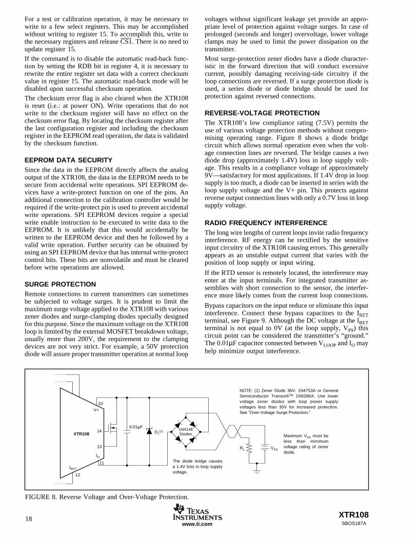
SURGE PROTECTIONRemote connections to current transmitters can sometimesbe subjected to voltage surges. It is prudent to limit themaximum surge voltage applied to the XTR108 with variouszener diodes and surge-clamping diodes specially designedfor this purpose. Since the maximum voltage on the XTR108loop is limited by the external MOSFET breakdown voltage,usually more than 200V, the requirement to the clampingdevices are not very strict. For example, a 50V protectiondiode will assure proper transmitter operation at normal loop
voltages without significant leakage yet provide an appro-priate level of protection against voltage surges. In case ofprolonged (seconds and longer) overvoltage, lower voltageclamps may be used to limit the power dissipation on thetransmitter.
Most surge-protection zener diodes have a diode character-istic in the forward direction that will conduct excessivecurrent, possibly damaging receiving-side circuitry if theloop connections are reversed. If a surge protection diode isused, a series diode or diode bridge should be used forprotection against reversed connections.
REVERSE-VOLTAGE PROTECTIONThe XTR108’s low compliance rating (7.5V) permits theuse of various voltage protection methods without compro-mising operating range. Figure 8 shows a diode bridgecircuit which allows normal operation even when the volt-age connection lines are reversed. The bridge causes a twodiode drop (approximately 1.4V) loss in loop supply volt-age. This results in a compliance voltage of approximately9V—satisfactory for most applications. If 1.4V drop in loopsupply is too much, a diode can be inserted in series with theloop supply voltage and the V+ pin. This protects againstreverse output connection lines with only a 0.7V loss in loopsupply voltage.
RADIO FREQUENCY INTERFERENCEThe long wire lengths of current loops invite radio frequencyinterference. RF energy can be rectified by the sensitiveinput circuitry of the XTR108 causing errors. This generallyappears as an unstable output current that varies with theposition of loop supply or input wiring.
If the RTD sensor is remotely located, the interference mayenter at the input terminals. For integrated transmitter as-semblies with short connection to the sensor, the interfer-ence more likely comes from the current loop connections.
Bypass capacitors on the input reduce or eliminate this inputinterference. Connect these bypass capacitors to the IRETterminal, see Figure 9. Although the DC voltage at the IRETterminal is not equal to 0V (at the loop supply, VPS) thiscircuit point can be considered the transmitter’s “ground.”The 0.01µF capacitor connected between VLOOP and IO mayhelp minimize output interference.
FIGURE 8. Reverse Voltage and Over-Voltage Protection.
XTR108
11
V+
IO
VPS
10
0.01µF
RL
D1(1)14
13
NOTE: (1) Zener Diode 36V: 1N4753A or General Semiconductor TransorbTM 1N6286A. Use lower voltage zener diodes with loop power supply voltages less than 30V for increased protection. See “Over-Voltage Surge Protection.”
Maximum VPS must be less than minimum voltage rating of zener diode.
The diode bridge causes a 1.4V loss in loop supply voltage.
1N4148Diodes
12
IRET
XTR108 19SBOS187A www.ti.com
EXCITATION CURRENT IREF
Coarse DAC code
N roundI R
VREF SET
REF11
64320=
•
–
Fine DAC Code
N roundI R
VNREF SET
REF10 11
10245120 16=
••
– –
ZERO OUTPUT IZERO
Coarse DAC Code
Fine DAC Code
N roundI R
VNZERO VI
REF12 13
512
52240 16=
••
•
– –
LINEARIZATION COEFFICIENT GLIN
Lin DAC Code
N round G RLIN LIN14 16= •( )
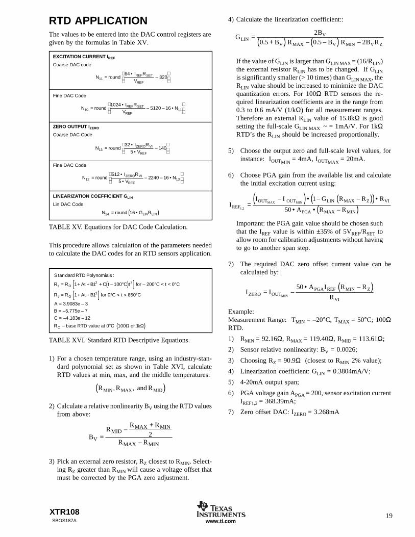
RTD APPLICATIONThe values to be entered into the DAC control registers aregiven by the formulas in Table XV.
This procedure allows calculation of the parameters neededto calculate the DAC codes for an RTD sensors application.
1) For a chosen temperature range, using an industry-stan-dard polynomial set as shown in Table XVI, calculateRTD values at min, max, and the middle temperatures:
R R and RMIN MAX MID, ,( )
2) Calculate a relative nonlinearity BV using the RTD valuesfrom above:
BR
R R
R RV
MIDMAX MIN
MAX MIN=
+–
–2
3) Pick an external zero resistor, RZ closest to RMIN. Select-ing RZ greater than RMIN will cause a voltage offset thatmust be corrected by the PGA zero adjustment.
4) Calculate the linearization coefficient::
GB
B R B R B RLINV
V MAX V MIN V Z
=+( ) ( )
2
0 5 0 5 2. – . – –
If the value of GLIN is larger than GLIN MAX = (16/RLIN)the external resistor RLIN has to be changed. If GLINis significantly smaller (> 10 times) than GLIN MAX, theRLIN value should be increased to minimize the DACquantization errors. For 100Ω RTD sensors the re-quired linearization coefficients are in the range from0.3 to 0.6 mA/V (1/kΩ) for all measurement ranges.Therefore an external RLIN value of 15.8kΩ is goodsetting the full-scale GLIN MAX ~ = 1mA/V. For 1kΩRTD’s the RLIN should be increased proportionally.
5) Choose the output zero and full-scale level values, forinstance: IOUTMIN
= 4mA, IOUTMAX = 20mA.
6) Choose PGA gain from the available list and calculatethe initial excitation current using:
II I G R R R
A R RREFOUT OUT LIN MAX Z VI
PGA MAX MIN
MAX MIN
1 2
1
50,
– – –
–=
( ) • ( )( ) •
• • ( )Important: the PGA gain value should be chosen suchthat the IREF value is within ±35% of 5VREF/RSET toallow room for calibration adjustments without havingto go to another span step.
7) The required DAC zero offset current value can becalculated by:
I IA I R R
RZERO OUTPGA REF MIN Z
VIMIN
=• ( )
––50
Example:Measurement Range: TMIN = –20°C, TMAX = 50°C; 100ΩRTD.
1) RMIN = 92.16Ω, RMAX = 119.40Ω, RMID = 113.61Ω;
2) Sensor relative nonlinearity: BV = 0.0026;
3) Choosing RZ = 90.9Ω (closest to RMIN 2% value);
4) Linearization coefficient: GLIN = 0.3804mA/V;
5) 4-20mA output span;
6) PGA voltage gain APGA = 200, sensor excitation currentIREF1,2 = 368.39mA;
7) Zero offset DAC: IZERO = 3.268mA
TABLE XV. Equations for DAC Code Calculation.
TABLE XVI. Standard RTD Descriptive Equations.
N roundI R
VZERO VI
REF13
32
5140=
••
–
S dard RTD Polynomials
R R At B C t C t for C t C
R R At B for C t C
A e
B e
C e
R base RTD value at C or k
t O
t O
O
tan :
– –
. –
– . –
– . –
–
= + + + °( )[ ] ° < < °
= + +[ ] ° < < °
===
° ( )
1 1 100 200 0
1 1 0 850
3 9083 3
5 775 7
4 183 12
0 100 1
2 3
2
Ω Ω
XTR10820SBOS187Awww.ti.com
CALIBRATION PROCEDURE FOR RTD SENSORS
Step 1 Initial parameters calculation.
• Using the procedure above, compute IREF, APGA, IZERO,and GLIN based on TMIN, TMAX, and nominal values ofRZ, RSET, and RVI. Use the equation in Table XV tocalculate the DAC register values.
• Configure the input MUX, write PGA gain, reference,and offset DAC registers of the XTR108 with calcu-lated settings. Note: write GLIN = 0 (no linearization) toXTR108 at this step;
Step 2 Measurement.
• Set RTD resistor value (or oven temperature) to mini-mum scale, measure output signal IMEAS1;
• Set RTD resistor value (or oven temperature) to maxi-mum scale, measure output signal IMEAS2;
Step 3.• Calculate corrections using the following equations:
II I R
A R R
R RI I R
A I
GB
B R B R B R
REFMEAS MEAS VI
PGA MAX MIN
Z MINZERO MEAS VI
PGA REFA
LINAV
V MAX V MIN V ZA
A
A
=( )
( )
= +( )
=+( ) ( )
2 1
1
50
50
2
0 5 0 5 2
–
–
–
. – . – –
II I G R R R
A R R
I I I I I
Adjusted I fine DAC Code N N roundI R
V
I I IA I
REFOUT OUT LIN A MAX Z VI
PGA MAX MIN
ZERO REF REF REF REF
REFREF SET
REF
ZERO OUT ZEROPGA
B
MAX MIN A
A B
A
MIN
=( ) • ( )( ) •
• • ( )= ( ) + ( )
= + •
=•
– – –
–
– –
:
– –
_1
50
1024
50
10 10
∆
∆
∆REFREF MIN Z
VI
REFZERO VI
REF
B A
A
R R
R
Adjusted I fine DAC Code N N roundI R
V
–
:
( )
= + ••
12 12
512
5
∆
This takes into account resistor value deviations, alloffsets and gain errors of the coarse DACs and PGA. Ifthe adjusted abs(N12A) > 128 or abs(N10A) > 128, adjustthe coarse DAC first, then recalculate the fine DACvalue;
• Update all the DAC register value, including lineariza-tion DAC.
Step 4 (optional).Measure output signal IMEAS3 with maximum RTD valuestill connected to the input from step 2;
Step 5 (optional).Compute GLIN correction and update LinDAC register;
Step 6 (optional).Make verification measurements at min- and max-inputsignal; If linearity check is needed: make a measurement atmid-scale; write EEPROM data.
Step 7.Set the desired over-scale, under-scale signal limits andsensor burnout indication configuration. Verify and adjustthe over-scale and under-scale levels by applying the posi-tive and negative overdriving differential signals to the PGAinputs.
XTR108 21SBOS187A www.ti.com
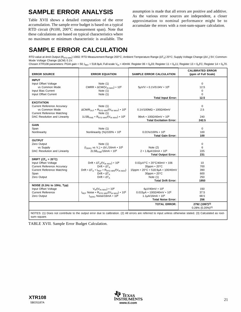
SAMPLE ERROR ANALYSISTable XVII shows a detailed computation of the erroraccumulation. The sample error budget is based on a typicalRTD circuit (Pt100, 200°C measurement span). Note thatthese calculations are based on typical characteristics whereno maximum or minimum characteristic is available. The
assumption is made that all errors are positive and additive.As the various error sources are independent, a closerapproximation to nominal performance might be toaccumulate the errors with a root-sum-square calculation.
CALIBRATED ERRORERROR SOURCE ERROR EQUATION SAMPLE ERROR CALCULATION (ppm of Full Scale)
INPUTInput Offset Voltage Note (1) 0
vs Common Mode CMRR • ∆CM/(VIN MAX) • 106 5µV/V • 0.1V/0.04V • 106 12.5Input Bias Current Note (1) 0Input Offset Current Note (1) 0
Total Input Error: 12.5
EXCITATIONCurrent Reference Accuracy Note (1) 0
vs Common Mode ∆CM/ROUT • RRTD MIN/(VIN MAX) • 106 0.1V/100MΩ • 100Ω/40mV 2.5Current Reference Matching Note (1)DAC Resolution and Linearity 1LSBFINE • RRTD MIN/(VIN MAX) • 106 96nA • 100Ω/40mV • 106 240
Total Excitation Error: 242.5
GAINSpan Note (1) 0Nonlinearity Nonlinearity (%)/100% • 106 0.01%/100% • 106 100
Total Gain Error: 100
OUTPUTZero Output Note (1) 0
vs Supply (IZERO vs V+) • ∆V+/16mA • 106 Note (2) 6DAC Resolution and Linearity 2LSBFINE/16mA • 106 2 • 1.8µA/16mA • 106 225
Total Output Error: 231
DRIFT (∆TA = 20°C)Input Offset Voltage Drift • ∆TA/(VIN MAX) • 106 0.02µV/°C • 20°C/40mV • 106 10Current Reference Accuracy Drift • ∆TA 35ppm • 20°C 700Current Reference Matching Drift • ∆TA • IREF • RRTD MIN/(VIN MAX) 15ppm • 20°C • 518.9µA • 100/40mV 390Span Drift • ∆TA 30ppm • 20°C 600Zero Output Drift • ∆TA Note (1) 250
Total Drift Error: 1950
NOISE (0.1Hz to 10Hz, Typ)Input Offset Voltage VN/(VIN MAX) • 106 6µV/40mV • 106 150Current Reference IREF Noise • RRTD MIN/(VIN MAX) • 106 0.015µA • 100Ω/40mV • 106 37.5Zero Output IZERO Noise/16mA • 106 1.1µA/16mA • 106 68.5
Total Noise Error: 256
TOTAL ERROR: 2792 (1997)(3)
0.28% (0.20%)(3)
SAMPLE ERROR CALCULATIONRTD value at 4mA Output (RRTD MIN) 100Ω: RTD Measurement Range 200°C; Ambient Temperature Range (∆TA) 20°C; Supply Voltage Change (∆V+) 5V; Common-Mode Voltage Change (∆CM) 0.1V.Chosen XTR108 parameters: PGIA gain = 50; IREF = 518.9µA; Full-scale VIN = 40mW. Register 06 = 0H03; Register 11 = 0H11; Register 13 = 0HFC; Register 14 = 0H70.
NOTES: (1) Does not contribute to the output error due to calibration. (2) All errors are referred to input unless otherwise stated. (3) Calculated as root-sum–square.
TABLE XVII. Sample Error Budget Calculation.
XTR10822SBOS187Awww.ti.com
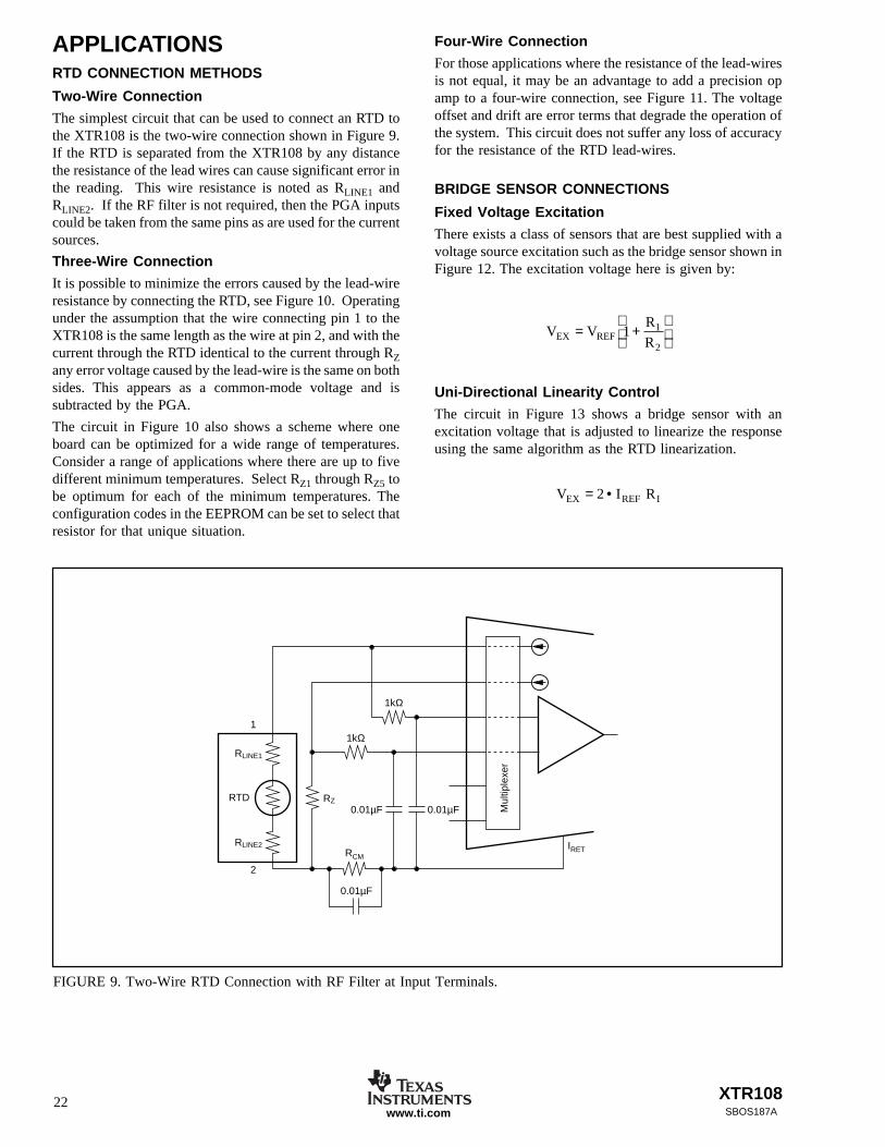
APPLICATIONSRTD CONNECTION METHODS
Two-Wire Connection
The simplest circuit that can be used to connect an RTD tothe XTR108 is the two-wire connection shown in Figure 9.If the RTD is separated from the XTR108 by any distancethe resistance of the lead wires can cause significant error inthe reading. This wire resistance is noted as RLINE1 andRLINE2. If the RF filter is not required, then the PGA inputscould be taken from the same pins as are used for the currentsources.
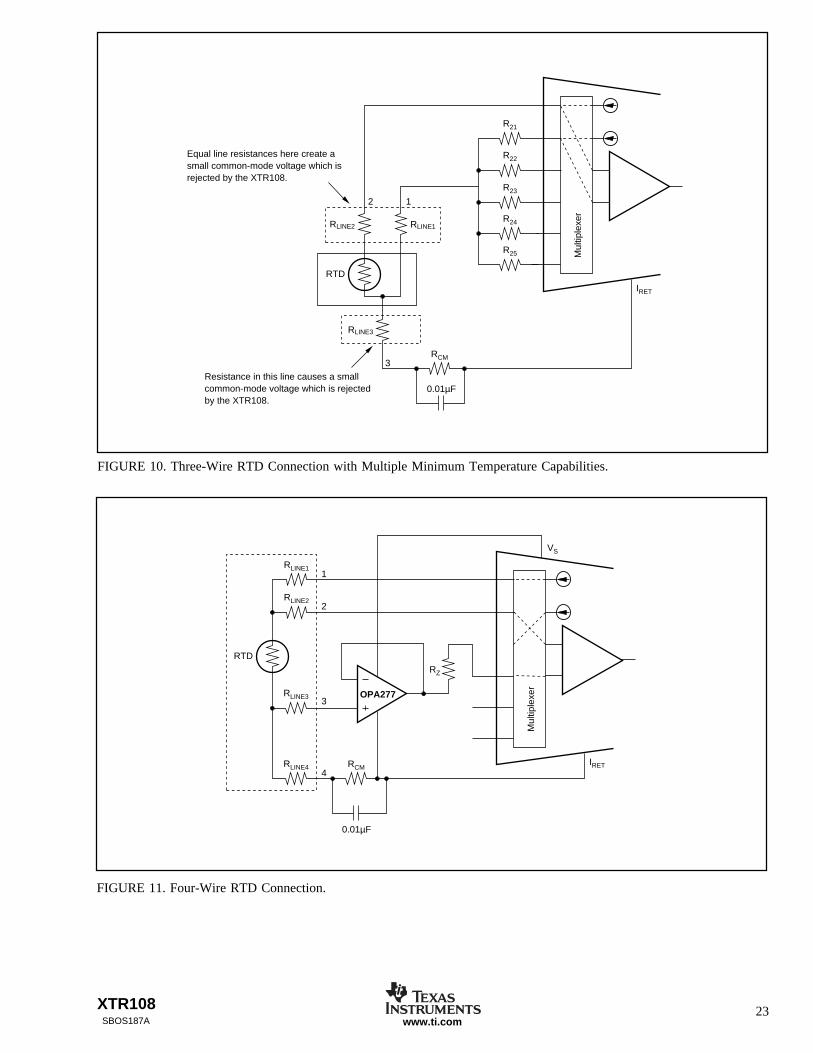
Three-Wire Connection
It is possible to minimize the errors caused by the lead-wireresistance by connecting the RTD, see Figure 10. Operatingunder the assumption that the wire connecting pin 1 to theXTR108 is the same length as the wire at pin 2, and with thecurrent through the RTD identical to the current through RZany error voltage caused by the lead-wire is the same on bothsides. This appears as a common-mode voltage and issubtracted by the PGA.
The circuit in Figure 10 also shows a scheme where oneboard can be optimized for a wide range of temperatures.Consider a range of applications where there are up to fivedifferent minimum temperatures. Select RZ1 through RZ5 tobe optimum for each of the minimum temperatures. Theconfiguration codes in the EEPROM can be set to select thatresistor for that unique situation.
Four-Wire Connection
For those applications where the resistance of the lead-wiresis not equal, it may be an advantage to add a precision opamp to a four-wire connection, see Figure 11. The voltageoffset and drift are error terms that degrade the operation ofthe system. This circuit does not suffer any loss of accuracyfor the resistance of the RTD lead-wires.
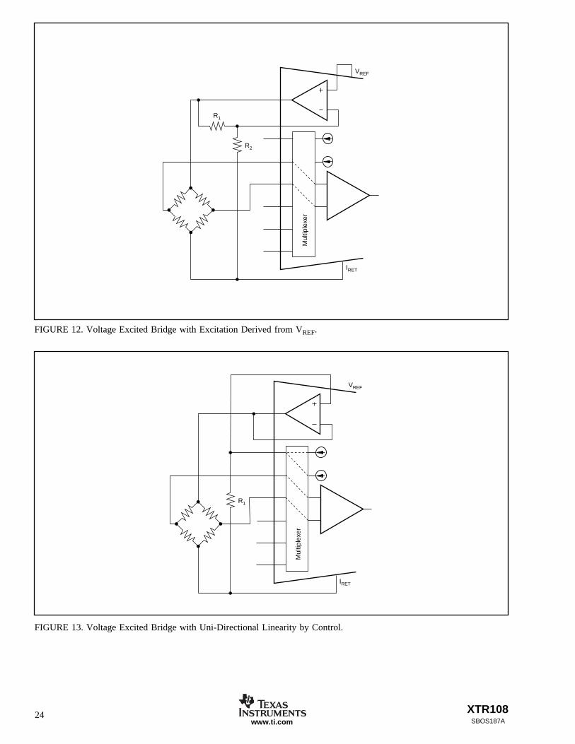
BRIDGE SENSOR CONNECTIONS
Fixed Voltage Excitation
There exists a class of sensors that are best supplied with avoltage source excitation such as the bridge sensor shown inFigure 12. The excitation voltage here is given by:
V VR
REX REF= +
1 1
2
Uni-Directional Linearity Control
The circuit in Figure 13 shows a bridge sensor with anexcitation voltage that is adjusted to linearize the responseusing the same algorithm as the RTD linearization.
V I REX REF I= •2
FIGURE 9. Two-Wire RTD Connection with RF Filter at Input Terminals.
Mul
tiple
xer
0.01µF0.01µF
1kΩ
1kΩ
RLINE2
RLINE1
RZ
1
2
RTD
RCMIRET
0.01µF
XTR108 23SBOS187A www.ti.com
FIGURE 10. Three-Wire RTD Connection with Multiple Minimum Temperature Capabilities.
FIGURE 11. Four-Wire RTD Connection.
Mul
tiple
xer
RLINE3
RLINE2 RLINE1
2 1
3
RTD
R21
R22
R23
R24
R25
RCM
IRET
0.01µF
Equal line resistances here create a small common-mode voltage which is rejected by the XTR108.
Resistance in this line causes a small common-mode voltage which is rejected by the XTR108.
Mul
tiple
xer
4
3
2
1
RTD
RCM
0.01µF
OPA277
IRET
VS
RLINE1
RZ
RLINE2
RLINE3
RLINE4
XTR10824SBOS187Awww.ti.com
FIGURE 12. Voltage Excited Bridge with Excitation Derived from VREF.
FIGURE 13. Voltage Excited Bridge with Uni-Directional Linearity by Control.
Mul
tiple
xer
IRET
VREF
R2
R1
Mul
tiple
xer
IRET
VREF
R1
XTR108 25SBOS187A www.ti.com
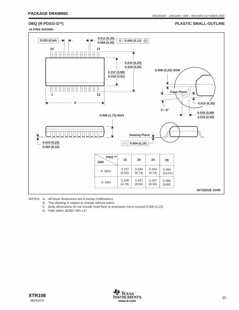
PACKAGE DRAWING MSOI004D – JANUARY 1995 – REVISED OCTOBER 2000
DBQ (R-PDSO-G**) PLASTIC SMALL-OUTLINE
Gage Plane
0.008 (0,20) NOM
0.010 (0,25)
0.016 (0,40)0.035 (0,89)
2420
Seating Plane
(8,74)
(8,56)0.3370.337
(8,56)
(8,74)0.344 0.344
4073301/E 10/00
13
0.150 (3,81)0.157 (3,99)
0.012 (0,30)0.008 (0,20)
12
A
24 PINS SHOWN
1
24
16DIM
PINS **
A MIN
A MAX
0.004 (0,10)0.010 (0,25)
0.069 (1,75) MAX
0.244 (6,20)0.228 (5,80)
0.197(5,00)
(4,78)0.188
0.004 (0,10)
M0.005 (0,13)0.025 (0,64)
0°–8°
28
(10,01)
(9,80)0.386
0.394
NOTES: A. All linear dimensions are in inches (millimeters).B. This drawing is subject to change without notice.C. Body dimensions do not include mold flash or protrusion not to exceed 0.006 (0,15).D. Falls within JEDEC MO-137

IMPORTANT NOTICE
Texas Instruments Incorporated and its subsidiaries (TI) reserve the right to make corrections, modifications,enhancements, improvements, and other changes to its products and services at any time and to discontinueany product or service without notice. Customers should obtain the latest relevant information before placingorders and should verify that such information is current and complete. All products are sold subject to TI’s termsand conditions of sale supplied at the time of order acknowledgment.
TI warrants performance of its hardware products to the specifications applicable at the time of sale inaccordance with TI’s standard warranty. Testing and other quality control techniques are used to the extent TIdeems necessary to support this warranty. Except where mandated by government requirements, testing of allparameters of each product is not necessarily performed.
TI assumes no liability for applications assistance or customer product design. Customers are responsible fortheir products and applications using TI components. To minimize the risks associated with customer productsand applications, customers should provide adequate design and operating safeguards.
TI does not warrant or represent that any license, either express or implied, is granted under any TI patent right,copyright, mask work right, or other TI intellectual property right relating to any combination, machine, or processin which TI products or services are used. Information published by TI regarding third–party products or servicesdoes not constitute a license from TI to use such products or services or a warranty or endorsement thereof.Use of such information may require a license from a third party under the patents or other intellectual propertyof the third party, or a license from TI under the patents or other intellectual property of TI.
Reproduction of information in TI data books or data sheets is permissible only if reproduction is withoutalteration and is accompanied by all associated warranties, conditions, limitations, and notices. Reproductionof this information with alteration is an unfair and deceptive business practice. TI is not responsible or liable forsuch altered documentation.
Resale of TI products or services with statements different from or beyond the parameters stated by TI for thatproduct or service voids all express and any implied warranties for the associated TI product or service andis an unfair and deceptive business practice. TI is not responsible or liable for any such statements.
Mailing Address:
Texas InstrumentsPost Office Box 655303Dallas, Texas 75265
Copyright 2001, Texas Instruments Incorporated