simulation methods of quantum-dot semiconductor optical amplifiers
TRANSCRIPT

Chapter 2Simulation Methods of Quantum-DotSemiconductor Optical Amplifiers
2.1 Introduction
In modeling a semiconductor optical amplifier, one would first consider how thecarrier dynamics are modeled. Secondly, one would be concerned about how tomodel the optical field propagation. There exist many SOA models of differentaccuracies. The most accurate way of modeling an SOA is to solve the semi-conductor bloch equation (SBE) but this is extremely time-consuming. Thecomputation time is not acceptable for the system applications of SOA-baseddevices, where many optical pulses have to be transmitted through the SOA toevaluate the system performance. A simplified approach is to include certainphysical processes phenomenologically, as it is done in rate-equation models.These models enjoy the much faster calculation speeds. Although the accuracy forsub-picosecond pulses is not as good as the SBE calculations, the rate equationmodels are quite successful in explaining the experimental results for both laserdiodes and SOAs. In early 1990s, Mørk et al. introduced the concept of the localcarrier density in the SOA modeling and by doing so, intra-band carrier dynamicssuch as spectral hole burning, carrier heating and free carrier absorption can bemodeled with great success to explain the pump-probe experimental results.
Numerical modeling is always necessary to understand the working principle ofthe devices and to optimize their performance. It is also useful to verify a novelidea before implementing it in the lab. It also allows the applications engineer topredict how an SOA or cascade of SOAs behaves in a particular application. Itmeans, physical modeling of complex devices including SOA, such as all-activeMZIs, is necessary in order to understand their potential and limitations. Inaddition, a reliable physical model may be used to investigate new configurationsleading to superior ways of operating devices, or possibly to development ofentirely new device structures.
The main purpose of modeling a SOA is to relate the internal variables of theamplifier to measurable external variables such as the output signal power,
A. Rostami et al., Nanostructure Semiconductor Optical Amplifiers,Engineering Materials, DOI: 10.1007/978-3-642-14925-2_2,� Springer-Verlag Berlin Heidelberg 2011
53

saturation output power and amplified spontaneous emission (ASE) spectrum. Thisaids the design and optimization of SOA for a given application. As the SOAmodel equations contain coupled derivatives of time and space, thus they haverarely analytical solutions. However, analytical solutions of SOA equations cangive a deep understanding on how internal variables of the device vary by externalconditions such as injection current, input pump, temperature, etc. Also, an ana-lytical solution may exactly exhibit the limitation of the operation since it containsthe influence of physical phenomena explicitly. Due to the mentioned difficultiesof obtaining an analytical solution, a numerical solution is required in most ofapplications.
Numerical techniques are usually more complex but make fewer assumptionsand are often applicable over a wide range of operating regimes. With the adventof fast personal computers, numerical techniques are beginning to supersedeanalytical techniques.
In spite of intensive research on numerical modeling of QD-SOAs, both the-oretically and experimentally, there still remains an unexplored area. This involvesthe development of equivalent circuit models for QD-SOAs suitable for circuitsimulation by using standard packages like SPICE. Considering the fact thatnumerical techniques as the solution of the rate equations require long and tediouscomputational time, analysis of equivalent circuit models with circuit programsreduces the computational time several orders.
In this chapter, we bring examples of modeling QD-SOAs by well-knownnumerical, analytical and equivalent circuits.
2.2 Numerical Methods
A comprehensive model should include the effect of several factors on QD-SOAperformance. Most of modeling methods consider quantum dots grown by theStranski–Krastanov mode as active region for QD-SOAs and thus some pre-sumptions are considered. In this manner, performance of QD-SOAs is primarilydominated by the dynamics of carriers and photons, like carrier relaxation, capture,re-excitation rate into quantum dots, radiative and non-radiative recombinationrates of carriers, inhomogeneous broadening of dot resonant energy due to sizefluctuation of dots, homogeneous broadening of optical gain due to polarizationdephasing rate, coulomb effects between electrons and holes and opticalnonlinearities.
The most popular and useful way to deal with carrier and photon dynamics inopto-electronic devices is to solve rate equations for carriers and photons. In themodeling process described in this section, quantum dots are considered to bespatially isolated and each quantum dot exchange carries with the wetting layer.Quantum dots are grouped by their resonant energy so that the model can justifythe inhomogeneously broadened gain spectra due to dot size fluctuation and thehomogeneous broadening of dots which originates from carrier-LO phonon andcarrier-carrier scatterings, has inserted into the rate equations. The homogeneous
54 2 Quantun-Dot Semiconductor Optical Amplifiers

broadening plays a crucial rule in processing applications and determines thechannel spacing in multi-wavelength operations [1]. Also, an interesting phe-nomenon happens in quantum dot lasers due to homogeneous broadening wherehomogeneous broadening of optical gain connects spatially isolated and energet-ically different quantum dots by bringing the carriers into the central lasing modeby stimulated emission and thus lasing emission with a narrower linewidth takesplace even compared with negligible homogeneous broadening case [2].
The schematic of inhomogeneously broadened quantum dot ensemble groupedby the resonant energy of dots and the related photon distribution is illustrated inFig. 2.1.
Different approaches have been introduced to treat electron and hole dynamics.In a vastly used model, one may consider an electron and a hole as an exciton anduse a common time constant for various processes [2, 3]. Separate consideration ofelectron and hole dynamics is another approach used in the researches [4].
By separate considering the electron and hole dynamics, one can develop ageneralized set of equations to consider the effect of different physical phenomenasuch as carrier doping [5]. So, this section introduces this approach by consideringseparate time constant for the processes associated with electrons and holes in aquantum dot structure.
Band diagram of a quantum dot group consisting discrete ground and excitedenergy levels, continuum like upper state (ensemble of dense energy states in eachdot which merge into the two-dimensional energy states of the wetting layer) andquantum well-type wetting layer is displayed in Fig. 2.2 where ground states,excited states and upper states are considered to be two-spin degenerate, fourfolddegenerate and many-fold degenerate respectively. Finally, quantum dots andphoton modes are divided into M (j = 1, …, M) and N (k = 1, …, N) groups,respectively.
The linear optical gain of ground or excited state of jth quantum dot group tokth photon mode can be expressed as
Fig. 2.1 Grouping of inho-mogeneously broadenedquantum dot ensemble andthe related photon modedistribution [5]
2.2 Numerical Methods 55

ggðeÞjk ¼ pq2
nbce0m20xk
pcvj j2DgðeÞNDGs
j
� Ch=ð2pÞðEc
gðeÞ;j � EvgðeÞ;j � �hxkÞ2 þ ðCh=2Þ2
ð1Þ
where pcv is the transition matrix element, c is the velocity of light, q is theelectron charge, m0 is the free electron mass, nb is the background refractive index,e0 is the permittivity of vacuum, ND is quantum dot volume density, Gj
s is thefraction of the radiative electron–hole recombination from the jth quantum dotgroup which has the Gaussian distribution with the FWHM ofCs = Cc ? Cv = 50 meV. The degeneracy of ground and excited states denotedby Dg(e) are Dg = 2 and De = 4 and their related energy in jth group are describedby Ec
gðeÞ;j, for conduction band and EvgðeÞ;j for valence band. Ch is the FWHM of
homogeneous broadening ranging from 16 to 19 meV in quantum dot lasers [2]and about 10 meV in quantum dot amplifiers [6]. As it is obvious in (1), a Lo-rentzian line shape function is used for the homogeneous broadening.
The transition matrix element (neglecting the optical-field polarization depen-dence) is expressed as
pcvj j2¼ Ic;v
����2�M2 ð2Þ
where Ic,v is the overlap integral between the envelope functions of an electron anda hole given by
M2 ¼ m20
12m�e
Eg E þ Dð ÞEg þ 2D=3
ð3Þ
Here, Eg is the band gap, D is the spin–orbit splitting energy and m�e is theelectron effective mass.
Fig. 2.2 Band diagram of aquantum dot group withmaximally allowable energystates defined by Ei,max [5]
56 2 Quantun-Dot Semiconductor Optical Amplifiers

The propagation of optical signal and the ASE along the QD-SOA can beexpressed by
oP xk; zð Þoz
¼ Cgðxk; zÞ � ai½ �P xk; zð Þ ð4Þ
oPsp xk; zð Þoz
¼ Cgðxk; zÞ � ai½ �Psp xk; zð Þ þ Cgsp xk; zð ÞPvac xkð Þ: ð5Þ
P, Psp, ai, C, gsp and Pvac are optical signal power, ASE power, intrinsic loss,confinement factor, optical gain for spontaneous emission and the optical power ofthe vacuum field between the frequency xk and xk ? Dx [7].
In self-assembled quantum dots, carriers are injected into the wetting layer andthen they are captured by upper states following with relaxation to excited andground states. Then, the carrier population dynamics of the wetting layer nc vð Þ
w , the
upper state nc vð Þu;j , the excited state nc vð Þ
e;j and the ground state nc vð Þg;j of the jth group
with corresponding occupation probabilities of f cðvÞw , f cðvÞ
u;j , f cðvÞe;j and f c vð Þ
g;j isdescribed by the following rate equations [5]
dncðvÞw
dt¼ J:A
qþX
j
ncðvÞu;j
scðvÞuw;j
1� f cðvÞw
� �
�X
j
ncðvÞw
scðvÞwu
GcðvÞj 1� f cðvÞ
u;j
� �
�ffiffiffiffiffiffiffiffiffiffinc
wnvw
p
swr
ð6Þ
dncðvÞu;j
dt¼ ncðvÞ
w
scðvÞwu
GcðvÞj 1� f cðvÞ
u;j
� �
�ncðvÞ
u;j
scðvÞuw
1� f cðvÞw
� �
þncðvÞ
e;j
scðvÞeu
1� f cðvÞu;j
� �
�ncðvÞ
u;j
scðvÞue
1� f cðvÞe;j
� �
þncðvÞ
g;j
scðvÞgu
1� f c ðvÞu;j
� �
�ncðvÞ
u;j
scðvÞug
1� f cðvÞg;j
� �
�ffiffiffiffiffiffiffiffiffiffiffiffiffinc
u;jnvu;j
p
sdr
ð7Þ
dncðvÞe;j
dt¼
ncðvÞu;j
scðvÞue
1� f cðvÞe;j
� �
�ncðvÞ
e;j
scðvÞeu
1� f cðvÞu;j
� �
þncðvÞ
g;j
scðvÞge
1� f cðvÞe;j
� �
�ncðvÞ
e;j
scðvÞeg
1� f cðvÞg;j
� �
�ffiffiffiffiffiffiffiffiffiffiffiffinc
e;jnve;j
p
sdr� CL
X
k
gejk
Pk
�hxkf ce;j þ f v
e;j � 1� �
ð8Þ
2.2 Numerical Methods 57

dncðvÞg;j
dt¼
ncðvÞu;j
scðvÞug
1� f cðvÞg;j
� �
�ncðvÞ
g;j
scðvÞgu
1� f cðvÞu;j
� �
þncðvÞ
e;j
scðvÞeg
1� f cðvÞg;j
� �
�ncðvÞ
g;j
scðvÞge
1� f cðvÞe;j
� �
�ffiffiffiffiffiffiffiffiffiffiffiffiffinc
g;jnvg;j
p
sdr� CL
X
k
ggjk
Pk
�hxkf cg;j þ f v
g;j � 1� �
:
ð9Þ
In above equations, J is the input injection current density and A is the crosssection area. The transition time constants for carriers are denoted by sxy
c(v) wherethe superscript c(v) stands for electron (hole) band and the subscript xy stands fortransition from state x to state y seg
c(v) determines the relaxation time from theexcited state to the ground state for instant). sdr and swr are the recombination timeconstants in dot and wetting layer, respectively. Typical value of parameters andtime constants used in the rate equations can be summarized as, swr = 0.2 ns,sdr = 1 ns, swu
c = 3 ps, suec = sug
c = segc = 1 ps, swu
v = suev = sug
v =segv = 0.13 ps,
Dg = 2, De = 4, Duc(v) = 10(20), Dw
c(v) = 100(200), ai = 5 cm-1 and C = 0.025.The value of time constants have obtained from the pump-probe experiments
[8], [9] and carrier escape times can be evaluated from the reported relaxation timeconstants through the relation
scðvÞyx ¼ scðvÞ
xy
Dy
Dxexp
DEcðvÞxy
kT
!
ð10Þ
where DExyc(v) is the energy difference between the state y and the state x in the
conduction (valence) band.
2.3 Equivalent Circuit Methods
In order to derive an equivalent circuit model of a QD-SOA one should firstdetermine band structure of the active region and then the governing rate equationof the active region should be obtained.
It is assumed that the QDs and WL are surrounded by a barrier material whichseparates the QD layers to the extent that the dot layers do not couple directly.Furthermore, tunneling between dots within the same layer is neglected. Thetransition of conduction band ground state (CBGS) to valence band ground state(VBGS) is assumed to be the main stimulated transition by input signal.
Band energy diagram of a quantum dot with related energy levels and intrabandrelaxation processes considered for extraction of rate equations and subsequentcircuit model is illustrated in Fig. 2.3. Here, the rate equations of the active regionmodel are written. The photon propagation equation of input signal and the
58 2 Quantun-Dot Semiconductor Optical Amplifiers

population dynamics of the wetting layer, the excited state and the ground state canbe written as [10]
oPs z; sð Þoz
¼ g� aintð ÞPs z; sð Þ ð11Þ
oNw z; sð Þos
¼ I
eV� Nw 1� hð Þ
sw2þ
~NQh
s2w� Nw
swRð12Þ
o~NQh z; sð Þos
¼ Nw 1� hð Þsw2
�~NQh
s2w�
~NQh 1� fð Þs21
þ~NQf 1� hð Þ
s12ð13Þ
o~NQf z; sð Þos
¼~NQh 1� fð Þ
s21�
~NQf 1� hð Þs12
�~NQf 2
s1R� g
r�hxsPs z; sð Þ ð14Þ
where Ps, g and aint are the optical power of input signal, the modal gain, theabsorption coefficient of material in signal wavelength, respectively and z is thedistance in longitudinal direction, i.e. z = 0 and z = L stand for input and outputfacets of the QD-SOA. �hx is the photon energy. Lw, r and V are the effectivethickness of active layer, cross section of the quantum dots or active layer and totalvolume of the quantum dots, respectively. NQ is the surface density of quantumdots where its typical value is *591010 cm-2 and ~NQ ¼ NQ=Lw is the effectivevolume density of quantum dots. Due to the larger effective mass of holes com-pared to electrons and resulting smaller level spacing, holes are expected to relaxfaster than electrons [11] and hence, electrons are assumed to limit the carrierdynamics.
The pump term in (12) is given as I/eV, with I being the bias current and e themagnitude of the electronic charge. Current is assumed to be injected directly intothe wetting layer and transport phenomena, such as drift or diffusion, are notexplicitly included in the model. swR is attributed to spontaneous recombinationtime, which contain contributions from nonradiative, radiative, and Augerrecombination. sw2 is the effective capture time and carrier capture is mediated byphonon and Auger processes. Phonon and Auger-assisted capture and relaxationcan be taken into account phenomenologically through the relation
Fig. 2.3 Band energy dia-gram of a quantum dot withrelated energy levels and in-traband relaxation processes[10]
2.3 Equivalent Circuit Methods 59

si = 1/(A ? CNw), i = w2, 21 where 1/A is the phonon-assisted capture (relaxa-tion) time and C is the coefficient determining the rate of Auger-assisted capture(relaxation) by scattering with carriers in the wetting layer. s2w is the characteristicescape time and s21, s12 are electron relaxation time from the excited state to theground state and escape time from the ground state to the excited state, respectivelyand s12 = s21 exp ((ES - EG)/kBT) where ES,G are the energies of the excited stateand ground state. s1R is spontaneous radiation lifetime in quantum dots.
The gain expression is given by g = gmax(fn ? fp - 1) where gmax is maximummodal gain [12] and can be defined as gmax ¼ Cl~NQa�1
P
iriðx0Þ where C is the
confinement factor, l is the number of quantum dot layers, a is the mean size of QDand ri(x0) is the effective cross section of the QDs at the signal frequency. fn(fp) isthe electron (hole) occupation probability in the GS. The term (fn ? fp - 1) is theeffective population inversion in GSs where the expressions of fn and fp are givenin [13]. For simplicity, fn = fp = f is assumed [14, 15]. Also hn(hp) is the electron(hole) occupation probability in the ES (hn = hp = h is presumed).
In order to achieve an input/output model of QD-SOA, we integrate the gainover the length of the device [16]. Therefore, the charge carrier density is supposedto be constant over the SOA length, Nw z; sð Þ ¼ Nw sð Þ; ~NQh z; sð Þ ¼ ~NQh sð Þ andalso~NQf z; sð Þ ¼ ~NQf sð Þ. Integration of the optical output relation reduces the SOAto a lumped element and averages the internal spatial information to single values,Nw sð Þ; ~NQh sð Þ and ~NQf sð Þ.
To relate the optical outputs at z = L to the inputs at z = 0, one may separatevariables of the propagation equation (11), integrate and normalize on [0, z], andsolve for the optical power at location z in terms of the input power
Ps z; sð Þ ¼ Ps 0; sð Þ expððg� aintÞzÞ ð15Þ
the optical output at the end of the device may describe as
Ps out sð Þ ¼ Ps in sð Þ expððg� aintÞLÞ ð16Þ
where L is the SOA length and Ps_in(s) = Ps (0, s), Ps_out(s) = Ps (L, s). Inte-grating the ground state rate equation (14) on z [ [0, L] and normalizing by 1/Lyields
d ~NQf sð Þds
¼~NQh 1� fð Þ
s21�
~NQf 1� hð Þs12
�~NQf 2
s1R� g
r�hx�Ps sð Þ ð17Þ
where Leibnitz’s rule has been employed to interchange the time derivative andthe spatial definite integral in (17) [17]. It is also defined that
�Ps sð Þ, 1L
ZL
0
Ps z; sð Þdz ð18Þ
and because f is assumed to be spatially invariant
60 2 Quantun-Dot Semiconductor Optical Amplifiers

�f sð Þ, 1L
ZL
0
f sð Þdz ð19Þ
is simply given by f(s) and the over script bar has omitted �f sð Þ ¼ f sð Þ. Substituting(15) into (18) gives
�Ps sð Þ ¼ Ps 0; sð Þ expððg� aintÞLÞ � 1½ �ðg� aintÞL
ð20Þ
So, by substituting (20) into the rate equation (17)
d~NQf sð Þds
¼~NQh 1� fð Þ
s21�
~NQf 1� hð Þs12
�~NQf 2
s1R
� gPs inðsÞ expððg� aintÞLÞ � 1½ �V�hxðg� aintÞ
ð21Þ
It is possible to rewrite the equations (12) and (13) in a similar mannerdescribed above.
Simple algebraic manipulation of new rate equations along with (15) yieldsequivalent circuit equations as
I ¼ C1dv1
dtþ v1
R4� k1v1v2 � k2v2 ð22Þ
k3v1 þ k4v3 þ k5v2v3 ¼ C2dv2
dtþ v2
R5þ k6v1v2 ð23Þ
k7v2 þ k8v2v3 ¼ C3dv3
dtþ v3
R3þ k9v2
3 þ fvs in½expðbðv3 � vtrf ÞÞ � 1� ð24Þ
vs out ¼ vs in expðbðv3 � vtrf ÞÞ ð25Þ
where the related parameters are listed below [18]
i1 ¼eVNw
sw2¼ v1
R1; i2 ¼
eV ~NQh
s21¼ v2
R2; i3 ¼
eV ~NQf
s12¼ v3
R3; i4 ¼
eVNw
swR¼ sw2
swRi1; i5
¼ eV ~NQh
s2w¼ s21
s2wi2; i6 ¼
eV ~NQf
s1R¼ s12
s1Ri3;
with R1 = R2 = R3 = 1X and R4 ¼ R1=ð1þ sw2=swRÞ;R5 ¼ R2=ð1þ s21=s2wÞ;C1 ¼ sw2=R1;C2 ¼ s21=R2;C3 ¼ s12=R3; k1 ¼ k6 ¼ s21=eV ~NQR1R2; k2 ¼ s21=s2w
R2; k3 ¼ 1=R1, R5 = R2/(1 ? s21/s2w), C1 = sw2/R1, C2 = s21/R2,C3 = s12/R3,k1 ¼ k6 ¼ s21=eV ~NQR1R2, k2 = s21/s2wR2, k3 = 1/R1, k4 = 1/R3, k5 ¼ ðs12 � s21Þ=eV ~NQR2R3, k7 = 1/R2, k8 ¼ ðs21 � s12Þ=eV ~NQR2R3, k9 ¼ s2
12=s1ReV ~NQR23,
f ¼ e2=sp�hxs, b ¼ 2gmaxs12L=eV ~NQR3,vtrf ¼ eV ~NQR3= 2s12, vs out ¼ spPs out=e,vs in ¼ spPs in=e with sp = 1.6 9 10-19 s.
2.3 Equivalent Circuit Methods 61

It is clear from above definitions that v1, v2 and v3 circuit voltages are pro-portional to Nw, h and f, respectively. Equations 22–25 can be employed todevelop the SPICE circuit model of the QD-SOA as shown in Fig. 2.4a–d withE1 = vs_in exp (b(v3 - vtrf)), G1 = k1v1v2, G2 = k2v2, G3 = k3v1, G4 = k4v3,G5 = k5v2v3, G6 = k6v1v2, G7 = k7v2, G8 = k8v2v3, G9 = k9v3
2, G10 = fvs_i-
n[ exp (b(v3 - vtrf)) - 1].The resistors Ris and Ros are arbitrary. Equations 22–24 are employed to construct
equivalent circuit models shown in Fig. 2.4b–d. Considering v1 as the node voltagein Eq. 22, the four right-hand terms of Eq. 22 are proportional to currents of acapacitor, resistor and voltage-dependant current sources (dependant on node volt-ages v1 and v2) with k1 and k2 coefficients, respectively and form the circuit model ofFig. 2.4b for instance. Equation 25 is used to form an equivalent sub-circuit modelfor Vs_out (related to the optical output power of QD-SOA) which is drawn inFig. 2.4a. These four sub-circuits are coupled to each other to determine the gainsaturation characteristics, output power, carrier dynamics and chirp of QD-SOA.
The current source I in Fig. 2.4b is proportional to the SOA bias current in (12),G1 dependant current source is dependent on v1 and v2 variables or Nw and h,respectively and is proportional to the Nwh/sw2 in (12). The dependant currentsource G2 is related to v2 variable which is proportional to ~NQh=s2wterm and C1
(capacitance) is the coefficient of wetting layer population variation (sw2/R1). All ofthe parameters can be obtained from other rate equations in a similar manner.
G7
Ris
G5
V3
Vs_in
G9
Vs_out
R4
(c)
G1
G3
RosE1
(d)
V1
C3
G2I
G10
V2
(a)
R3
R5
C1
C2
G8
G4 G6
(b)
Fig. 2.4 (a) SPICE sub-cir-cuit model to determine theoptical output power. (b)–(d)Equivalent sub-circuits tomeasure V1, V2 and V3,respectively, due to the biascurrent and Vs_in [10]
62 2 Quantun-Dot Semiconductor Optical Amplifiers

To investigate the accuracy of the equivalent circuit model, the gain saturationcharacteristics, the output pulse shape, the state occupation probabilities and thefrequency chirping of the QD-SOA have obtained using SPICE package using thetypical parameters given in [19, 20].
The saturation properties with the considered parameters for different biascurrents are illustrated in Fig. 2.5. The gain approaches its unsaturated value, G0,for small optical powers; in present case G0 & 19 dB. As the input power (andconsequently the output power) is increased, the gain starts to saturate andeventually the amplifier is forced toward transparency.
The output power at which the gain decrease by 3 dB, i.e., at Gsat = G0/2 isconsidered as output saturated power.
Beside the saturation properties, the temporal shape of amplified pulse and thegain dynamic have great importance in QD-SOA operation. As the pulse isamplified inside the SOA, the pulse shape becomes asymmetric due to variation inelectronic level population and the leading edge becomes sharper compared withthe trailing edge. Sharpening of the leading edge is a common feature of allamplifiers and occurs because the leading edge experiences larger gain thantrailing edge [21]. This fact is clear in Fig. 2.6 where the output pulse shape of aninput Gaussian pulse is plotted.
Fast gain dynamic is the other issue that should be addressed. The explanationfor the fast gain recovery can be seen in Fig. 2.7, which shows the variations of thecarrier densities of the three different levels during the amplification of the stronginput pulse. As carriers of ground state are removed through stimulated emissionthe excited state acts as a nearby carrier reservoir and enables ultrafast gainrecovery. Since the process of carrier capture is slower than intra-dot relaxation,the excited state recovers on a longer time-scale of several picoseconds which isthe upper limit for fast gain recovery time. The long recovery time of the wettinglayer is depicted in the inset of Fig. 2.7 which is in several hundred picosecondstimescale.
Since the gain change of SOAs gives rise to changes in the refractive index, asignal that has been amplified or processed with an SOA has a large frequency
Fig. 2.5 Gain saturationcharacteristics of a QD-SOAfor CW beam amplification,with the SOA gain plotted asa function of the outputpower, Pout, for differentpump current I in the SOA[10]
2.3 Equivalent Circuit Methods 63

chirp at the leading and trailing edges of the signal pulse. Figures 2.8 and 2.9 showthe frequency chirp of the amplified pulses for two input pulse trains at linear(Ps_in = 10 lW (peak value)) and nonlinear (Ps_in = 10mW) operation regions ofthe QD-SOA. The obtained results for frequency chirp, saturation power and gainrecovery process agree well with reported results in mentioned reports (Thenegligible mismatch is due to aint = 0 assumption).
Fig. 2.6 Output pulse shapeof a QD-SOA when aGaussian pulse passesthrough the amplifier [10]
Fig. 2.7 Simulated evolutionof occupation probability forthe ground state, the excitedstate and the wetting layer ofthe QD-SOA. The insetshows the slow dynamics ofthe wetting layer [10]
Fig. 2.8 Output power(pulse pattern) and chirp of apulse train passing throughthe QD-SOA operating in itslinear gain regime,Ps_in = 10 lW [10]
64 2 Quantun-Dot Semiconductor Optical Amplifiers

2.4 Analytical Methods
Most of the successful models in predicting the optical properties of QD-SOAstreat quantum dots as three-state systems and describe the SOA dynamics based ontransitions between the ground state, the excited state and the wetting layer.Therefore, a comprehensive analytical solution for explanation of the operationcharacteristics of QD-SOAs should take into account the carrier transitionsbetween these three states. The quantum dot model for active region of QD-SOAin this section comprises two nondegenerate energy states (ground and excitedstates) similar to the model introduced in the previous section. Signal propagationequation through the SOA length and also the rate equations for state occupationprobabilities may describe as [22]
oS
oz¼ gGSð�hxÞð2f � 1Þ þ gESð�hxÞð2h� 1Þ � a½ �S ð26Þ
of
ot¼ ð1� f Þh
s10� f ð1� hÞ
s01
� �
ða10 þ c10wÞ � f 2
s0R
� vggGSð�hxÞð2f � 1ÞSNQ
ð27Þ
oh
ot¼ ð1� hÞw
s21� hð1� wÞ
s12
� �
ða21 þ c21wÞ
� ð1� f Þhs10
� f ð1� hÞs01
� �
ða10 þ c10wÞ
� h2
s1R� vggESð�hxÞð2h� 1ÞS
NQ
ð28Þ
ow
ot¼ J
s0R� ð1� hÞw
s21� hð1� wÞ
s12
� �
ða21 þ c21wÞ
� w
swRðaw þ bwwþ cww2Þ
ð29Þ
Fig. 2.9 Output power(pulse pattern) and chirp of apulse train passing throughthe QD-SOA operating in itsnonlinear gain regime,Ps_in = 10 mW [10]
2.4 Analytical Methods 65

The occupation probabilities of the ground state, the excited state and thewetting layer at the band edge are expressed by f, h and w respectively, S isthe photon density, a is the waveguide loss, gGS and gES are the modal gain of theground and excited states. The phonon-assisted and Auger-assisted processes areincluded in the rate equations via a10, a21, aw and c10, c21, cw coefficients. Carrierrelaxation and excitation processes are denoted by s01, s10, s21, s12, s0R, s1R andswR as scape time from the GS to the ES, relaxation time from the ES to the GS,relaxation time from the WL to the ES, escape time from the ES to the WL,spontaneous radiative lifetimes in the GS, ES and WL respectively. NQ is thequantum dot volume density and J is normalized injection current density (J =
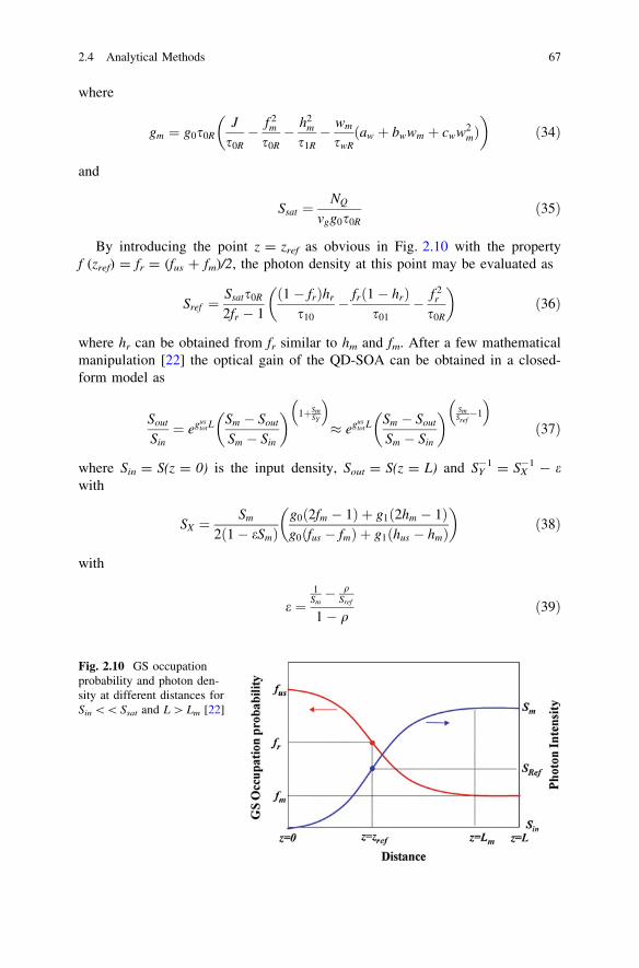
(I 9 s0R)/ qVaNWL where Va is the volume and NWL is the carrier density of the WL).Figure 2.10 describes the variation of the GS occupation probability and photon
intensity during SOA length at specified points. When a signal is injected to theSOA at z = 0, it experiences unsaturated gain. During the propagation of thesignal inside the SOA, the material gain will be decreased and for z [ Lm this gainwill be equal to material loss. Thus, for z [ Lm SOA will be transparent. Mean-while, the photon intensity increases during the pulse propagation due to stimu-lated emission and reaches to its maximum value for z [ Lm.
Therefore, the maximum output density of the devices is expected when thetotal gain equals with the material loss or gtot = a. Since the values of the GSoccupation probability and the photon intensity at z = 0, zref, Lm and L will be usedto obtain output and threshold characteristics of the SOA, It is useful to definef (z = Lm) = fm, h (z = Lm) = hm, and S (z = Lm) = Sm. Considering the photonenergy given by �hx0 and defining gGSð�hx0Þ ¼ g0 and gESð�hx0Þ ¼ g1 and findingthe roots of equation (27) - (29) for S = 0, one may obtain the unsaturatedoccupation probabilities of the GS, ES and WL. It should be noted that this methodis valid at steady state and for CW condition where the time derivatives of thecarrier rate equations can be set to zero. After evaluating the unsaturated occu-pation probabilities as fus, hus and Wus, the total unsaturated material gain andoptical gain of the amplifier may rewrite as
gustot ¼ g0ð2fus � 1Þ þ g1ð2hus � 1Þ � a ð30Þ
Gus ¼ expðgustot LÞ ð31Þ
and at the z = Lm
fm ¼12
1þ ag0
� �
� g1ð2hm � 1Þ2g0
: ð32Þ
By replacing the above expression for fm in (28) and (29), hm and wm can beextracted and the maximum output density at z = Lm can be extracted from (27) as(by finding the equivalent value for the expression between parentheses of (29) andreplacing in (28) and doing so for (28) and (27)
Sm ¼gm
aSsat ð33Þ
66 2 Quantun-Dot Semiconductor Optical Amplifiers
where
gm ¼ g0s0RJ
s0R� f 2
m
s0R� h2
m
s1R� wm
swRðaw þ bwwm þ cww2
m� �
ð34Þ
and
Ssat ¼NQ
vgg0s0Rð35Þ
By introducing the point z = zref as obvious in Fig. 2.10 with the propertyf (zref) = fr = (fus ? fm)/2, the photon density at this point may be evaluated as
Sref ¼Ssats0R
2fr � 1ð1� frÞhr
s10� frð1� hrÞ
s01� f 2
r
s0R
� �
ð36Þ
where hr can be obtained from fr similar to hm and fm. After a few mathematicalmanipulation [22] the optical gain of the QD-SOA can be obtained in a closed-form model as
Sout
Sin¼ egus
totLSm � Sout
Sm � Sin
� � 1þSmSY
� �
� egustotL
Sm � Sout
Sm � Sin
� � SmSref�1
� �
ð37Þ
where Sin = S(z = 0) is the input density, Sout = S(z = L) and SY-1 = SX
-1 - ewith
SX ¼Sm
2ð1� eSmÞg0ð2fm � 1Þ þ g1ð2hm � 1Þg0ðfus � fmÞ þ g1ðhus � hmÞ
� �
ð38Þ
with
e ¼1
Sm� q
Sref
1� qð39Þ
Fig. 2.10 GS occupationprobability and photon den-sity at different distances forSin \\ Ssat and L [ Lm [22]
2.4 Analytical Methods 67

and
q ¼ g0ð2fm � 1Þ þ g1ð2hm � 1Þ½ � g0ðfus � frÞ þ g1ðhus � hrÞ½ �g0ð2fr � 1Þ þ g1ð2hr � 1Þ½ � g0ðfus � fmÞ þ g1ðhus � hmÞ½ �: ð40Þ
Therefore, the optical gain of the QD-SOA can be obtained analytically only ifSm, Sref and the unsaturated optical gain are known. The output optical gain of theQD-SOA with analytically obtained solution and also with numerical solution ofthe rate equations using fourth-order Runge–Kutta method have plotted inFig. 2.11 to compare the accuracy of the solutions.
The following parameters have been used in the simulation; s0R =
s1R = swR = 0.2 ns, s10 = 8 ps, s21 = 2 ps, s01 = 80 ps, s12 = 20 ps, a =
3 cm-1, a10 = a21 = aw = 1, bw = cw = 0, c10 = c21 = 80, NQ = 2.5 9 1017
cm3, vg = 8.45 9 109 cm/s, g0 = 14 cm-1 and g1 = 14 cm-1. The photonintensity as a function of SOA length is also presented in Fig. 2.12 for bothnumerical and analytical methods.
Fig. 2.11 Optical gain of theQD-SOA versus devicelength for three differentapplied current values. TheSolid lines present the resultsof analytical method anddashed lines are for numericalmethod [22]
Fig. 2.12 Photon densityversus SOA length for twodifferent input signal intensi-ties. The Solid lines presentthe results of analyticalmethod and dashed lines arefor numerical method [22]
68 2 Quantun-Dot Semiconductor Optical Amplifiers

By defining the maximum SOA length as the length when the maximum outputis 3 dB less than Sm (Sout = 0.5 9 Sm), one can express an analytical formula forSOA length after which the device provided no gain. Hence, this criteria can bedefined from (37) as
L\1
gustot
ln0:5Sm
Smaxin
Sm � Smaxin
Sm � 0:5Sm
� 1þSmSY
� �0
B@
1
CA ð41Þ
As it is obvious from Fig. 2.11, this length is about 1 cm for the given deviceand for z [ 1 cm the SOA will be transparent.
References
1. Sugawara, M., Hatori, N., Akiyama, T., Nakata, Y., Ishikawa, H.: Quantum-dotsemiconductor optical amplifiers for high bit-rate signal processing over 40 Gbit/s. Jpn.J. Appl. Phys. 40, L488–L491 (2001)
2. Sugawara, M., Mukai, K., Nakata, Y., Ishikawa, H.: Effect of homogeneous broadening ofoptical gain on lasing spectra in self-assembled InxGa1-xAs/GaAs quantum dot lasers. Phys.Rev. B 61, 7595–7603 (2000)
3. Bilenca, A., Eisenstein, G.: On the noise properties of linear and nonlinear quantum-dotsemiconductor optical amplifiers: The impact of inhomogeneously broadened gain and fastcarrier dynamics. IEEE J. Quantum Electron 40, 690–702 (2004)
4. van der Poel, M., Gehrig, E., Hess, O., Birkedal, D., Hvam, J.M.: Ultrafast gain dynamics inquantum-dot amplifiers: Theoretical analysis and experimental investigations. IEEEJ. Quantum Electron 41, 1115–1123 (2005)
5. Kim, J., Laemmlin, M., Meuer, C., Bimberg, D., Eisenstein, G.: Theoretical and experimentalstudy of high-speed small-signal cross-gain modulation of quantum-dot semiconductoroptical amplifiers. IEEE J. Quantum Electron 45, 240–248 (2009)
6. Borri, P., Langbein, W., Schneider, S., Woggon, U., Sellin, R.L., Ouyang, D., Bimberg, D.:Exciton relaxation and dephasing in quantum-dot amplifiers from room-to cryogenictemperature. IEEE J. Sel. Topics Quantum Electron 8, 984–991 (2002)
7. Sugawara, M., Ebe, H., Hatori, N., Ishida, M., Arakawa, Y., Akiyama, T., Otsubo, K.,Nakata, Y.: Theory of optical signal amplification and processing by quantum-dotsemiconductor optical amplifiers. Phys. Rev. B 69, 235332-1-39 (2004)
8. Borri, P., Schneider, S., Langbein, W., Bimberg, D.: Ultrafast carrier dynamics in InGaAsquantum dot materials and devices. J. Opt. A 8, S33–S46 (2006)
9. Dommers, S., Temnov, V.V., Woggon, U., Gomis, J., Martinez-Pastor, J., Laemmlin, M.,Bimberg, D.: Complete ground state gain recovery after ultrashort double pulses in quantumdot based semiconductor optical amplifier. Appl. Phys. Lett. 90, 033508 (2007)
10. Maram, R., Baghban, H., Rasooli, H., Ghorbani, R., Rostami, A.: Equivalent circuit model ofquantum dot semiconductor optical amplifiers: dynamic behaviour and saturation properties.J. Opt. A 11, 105205-1-8 (2009)
11. Sosnowski, T.S., Norris, T.B., Jiang, H., Singh, J., Kamath, K., Bhattacharya, P.: Rapidcarrier relaxation in In0.4Ga0.6As/GaAs quantum dots characterized by differentialtransmission spectroscopy. Phys. Rev. B 57, R9423–R9426 (1998)
12. Steiner, T. (ed.): Semiconductor Nanostructures for Optoelectronic Applications. ArtechHouse, London (2004)
2.4 Analytical Methods 69

13. Asryan, L.V., Suris, R.A.: Longitudinal spatial hole burning in a quantum-dot laser. IEEE J.Quantum Electron 36, 1151–1160 (2000)
14. Qasaimeh, Q.: Characteristics of cross-gain (XG) wavelength conversion in quantum dotsemiconductor optical amplifiers. IEEE Photon. Technol. Lett. 16, 542-544 (2004)
15. Qasaimeh, O.: Optical gain and saturation characteristics of quantum-dot semiconductoroptical amplifiers. IEEE J. Quantum Electron. 39, 793–798 (2003)
16. Saleh, A.A.M.: Nonlinear models of travelling-wave optical amplifiers. Electron Lett. 24,835–837 (1988)
17. Kuntze, S.B., Pavel, L., Aitchison, J.S.: Controlling a semiconductor optical amplifier using astate-space model. IEEE J. Quantum Electron 43, 123–129 (2007)
18. Biswas, A., Basu, P.K.: Equivalent circuit models of quantum cascade lasers for SPICEsimulation of steady state and dynamic responses. J. Opt. A 9, 26–32 (2007)
19. Li X., Li, G.: Comments on ‘‘theoretical analysis of gain-recovery time and chirp inQD-SOA’’. IEEE Photon. Technol. Lett. 18, 2434–2435 (2006)
20. Ben-Ezra, Y., Haridim, M., Lembrikov, B.I.: Theoretical analysis of gain-recovery time andchirp in QD-SOA. IEEE Photon. Technol. Lett. 17, 1803–1805 (2005)
21. Agrawal, G.P., Olsson, N.A.: Self-phase modulation and spectral broadening of optical pulsesin semiconductor laser amplifiers. IEEE J. Quantum Electron 25, 2297–2306 (1989)
22. Qasaimeh, O.: Novel closed-form model for multiple-state quantum-dot semiconductoroptical amplifiers. IEEE J. Quantum Electron 44, 652–657 (2008)
70 2 Quantun-Dot Semiconductor Optical Amplifiers

http://www.springer.com/978-3-642-14924-5