optical computing with semiconductor optical amplifiers · optical computing with semiconductor...
TRANSCRIPT
Optical computing with semiconductoroptical amplifiers
Rekha MehraShikha JaiswalHemant Kumar Dixit
Downloaded From: https://www.spiedigitallibrary.org/journals/Optical-Engineering on 6/5/2018 Terms of Use: https://www.spiedigitallibrary.org/terms-of-use
Optical computing with semiconductor optical amplifiers
Rekha MehraGovernment Engineering CollegeDepartment of Electronics and CommunicationAjmer, IndiaE-mail: [email protected]
Shikha JaiswalChaudhary Charan Singh University, SD(PG)
CollegeDepartment of PhysicsMuzaffarnagar, India
Hemant Kumar DixitUniversity of AllahabadDepartment of Electronics and CommunicationAllahabad 211002, India
Abstract. Increasing communication traffic and plans to increase variousservices may cause a serious problem towards the power consumption ofnetwork equipment. One of the causes of large power consumption in thepresent network is the multiplexing scheme, such as wavelength divisionmultiplexing (WDM) and electrical routing of the packet signals. WDMrequires O/E (optical to electrical) and E/O (electrical to optical) signal con-version circuits with the same number as that of wavelength, resulting inan increase in power consumption. In addition to this electrical signal pro-cessing for the IP packet, routing, and switching at the router consumes alarge amount of power. If we could process ultrafast signals using electro-magnetic light waves without converting to electrical signals, this wouldreduce the power consumption of routers. One of the ways to overcomethese problems is the development of all-optical computing devices.All-optical computing devices are based on the nonlinear interaction oflight waves, which is an electromagnetic wave. The use of electromagneticlight waves makes computing, such as switching, possible at very highfrequencies of more than 100 GHz. We discuss all-optical computingdevices based on semiconductor optical amplifiers with the mainemphasis on all-optical logic gates. © 2012 Society of Photo-Optical InstrumentationEngineers (SPIE). [DOI: 10.1117/1.OE.51.8.080901]
Subject terms: semiconductor optical amplifier; cross gain modulation; four wavemixing; Mach–Zehnder interferometer; cross phase modulation.
Paper 120287V received Mar. 9, 2012; revised manuscript received Jun. 1, 2012;accepted for publication Jul. 6, 2012; published online Jul. 25, 2012.
1 IntroductionWith the tremendous growth of computing technology,the need of high-performance computers has significantlyincreased. Optics has been used in computing for a numberof years. Optical computing was a hot research area in1980’s, but the work tapered off due to material limitationsthat prevented opto chips from getting small enough andcheap enough beyond laboratory curiosities. Now, develop-ments in the field of optical computers are back with thedevelopment of nonlinear organic material and semiconduc-tor technology.1 The semiconductor optical amplifier (SOA)is one of the most frequently used devices for ultrafast all-optical computing. In the SOA, population inversion is rea-lized by current injection. When we put in an intense gatepulse, it causes gain reduction and an associated refractiveindex change takes place. This is the third-order nonlineareffect.
A characteristic feature of this response is that it is veryfast for the rise time; however, there is a slow component onthe order of 1 ns in the response recovery, which is the band-to-band recombination lifetime. This slow component hasbeen the obstacle in realizing ultrafast switching devicesabove 100 Gb∕s.2 Two methods are described for solvingthis problem. One is to use a wavelength filter to selectonly the very fast component of the response. Anothermethod is to use the SOA in a Mach–Zehnder interferometerconfiguration.
This paper discusses the properties of SOAs and howthese properties can be utilized to develop all-optical com-puting devices. In Sec. 2, a brief review of the basic
properties of SOAs and its features as an ultrafast nonlineardevice have been discussed. Section 3 introduces two waysof using SOAs for ultrafast signal processing: one is to useonly the very fast response component of SOAs with wave-length filter and the other is to cancel out the slow responsecomponent of SOAs using the Mach–Zehnder interferometerconfiguration. We review the progresses in SOA-based all-optical computing devices using the above two concepts. Outof the research papers based on similar methods, few havebeen included in the list of references as there is a lot ofresearch work going on in these techniques. Section 4describes the simulation results for the gain saturation char-acteristic of SOAs, which is the main characteristic for usingSOAs in optical computing devices.
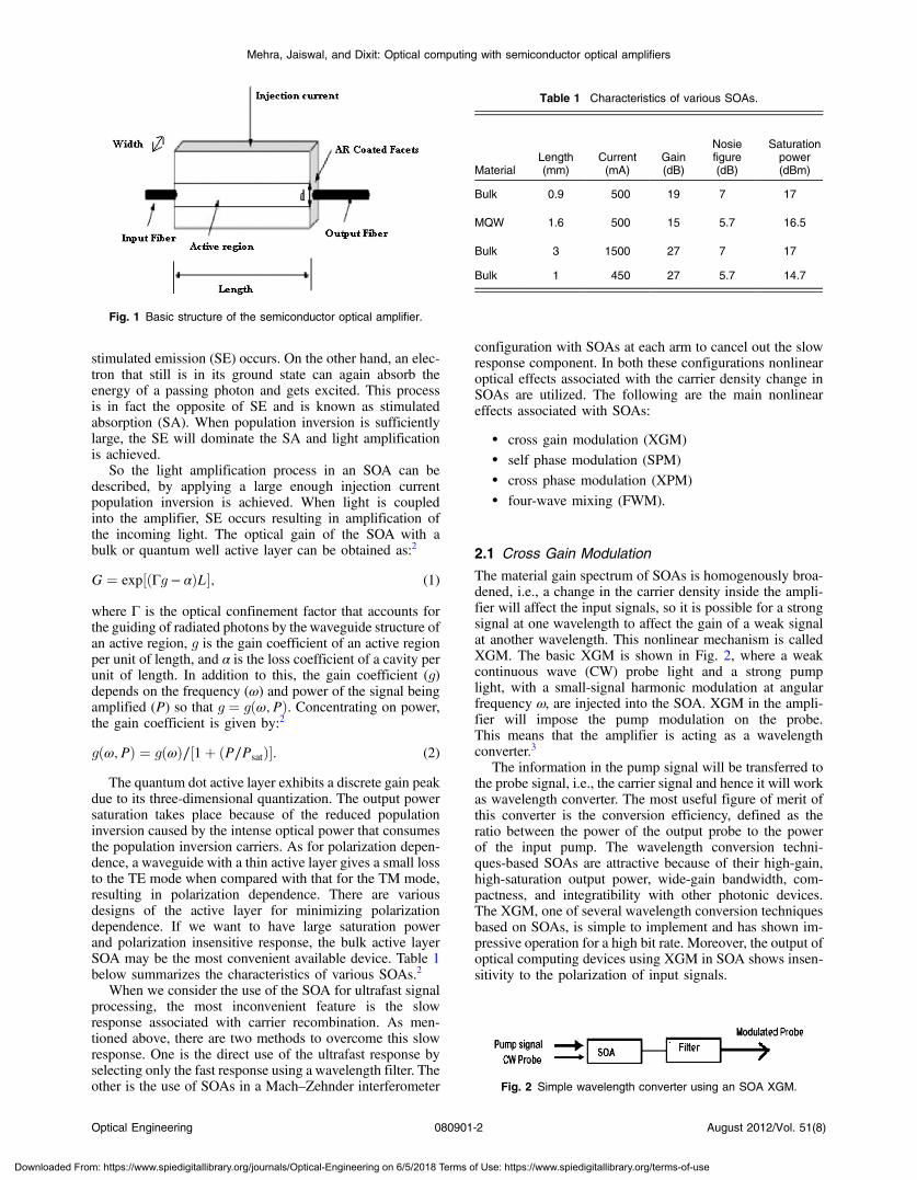
2 SOAs as an Ultrafast Nonlinear DeviceThe basic structure of a SOA is given in Fig. 1. An intrinsiclayer called the active layer is sandwiched between p-typematerial and n-type material layers. By selecting a differentmaterial composition for the active layer, it is possible to cre-ate a lower band gap with respect to its surrounding layers.When a forward voltage is applied over this heterostructure,free electrons from the n-type material and holes from thep-type material will travel towards the active layer. Herethe electrical carriers will accumulate as they are trappedin this low band gap potential well. By applying appropriatepumping, large concentrations of electrons and holes buildup in the active layer, which leads to population inversion.Photons from incoming light passing through the amplifiermedium can trigger electrons in the conduction band to relaxto their ground state and recombine with holes in the valenceband. As a result, photons with the same wavelength andphase as the incoming photons will be emitted and0091-3286/2012/$25.00 © 2012 SPIE
Optical Engineering 080901-1 August 2012/Vol. 51(8)
Optical Engineering 51(8), 080901 (August 2012) REVIEW
Downloaded From: https://www.spiedigitallibrary.org/journals/Optical-Engineering on 6/5/2018 Terms of Use: https://www.spiedigitallibrary.org/terms-of-use
stimulated emission (SE) occurs. On the other hand, an elec-tron that still is in its ground state can again absorb theenergy of a passing photon and gets excited. This processis in fact the opposite of SE and is known as stimulatedabsorption (SA). When population inversion is sufficientlylarge, the SE will dominate the SA and light amplificationis achieved.
So the light amplification process in an SOA can bedescribed, by applying a large enough injection currentpopulation inversion is achieved. When light is coupledinto the amplifier, SE occurs resulting in amplification ofthe incoming light. The optical gain of the SOA with abulk or quantum well active layer can be obtained as:2
G ¼ exp½ðΓg − αÞL�; (1)
where Γ is the optical confinement factor that accounts forthe guiding of radiated photons by the waveguide structure ofan active region, g is the gain coefficient of an active regionper unit of length, and α is the loss coefficient of a cavity perunit of length. In addition to this, the gain coefficient (g)depends on the frequency (ω) and power of the signal beingamplified (P) so that g ¼ gðω; PÞ. Concentrating on power,the gain coefficient is given by:2
gðω; PÞ ¼ gðωÞ∕½1þ ðP∕PsatÞ�: (2)
The quantum dot active layer exhibits a discrete gain peakdue to its three-dimensional quantization. The output powersaturation takes place because of the reduced populationinversion caused by the intense optical power that consumesthe population inversion carriers. As for polarization depen-dence, a waveguide with a thin active layer gives a small lossto the TE mode when compared with that for the TM mode,resulting in polarization dependence. There are variousdesigns of the active layer for minimizing polarizationdependence. If we want to have large saturation powerand polarization insensitive response, the bulk active layerSOA may be the most convenient available device. Table 1below summarizes the characteristics of various SOAs.2
When we consider the use of the SOA for ultrafast signalprocessing, the most inconvenient feature is the slowresponse associated with carrier recombination. As men-tioned above, there are two methods to overcome this slowresponse. One is the direct use of the ultrafast response byselecting only the fast response using a wavelength filter. Theother is the use of SOAs in a Mach–Zehnder interferometer
configuration with SOAs at each arm to cancel out the slowresponse component. In both these configurations nonlinearoptical effects associated with the carrier density change inSOAs are utilized. The following are the main nonlineareffects associated with SOAs:
• cross gain modulation (XGM)• self phase modulation (SPM)• cross phase modulation (XPM)• four-wave mixing (FWM).
2.1 Cross Gain Modulation
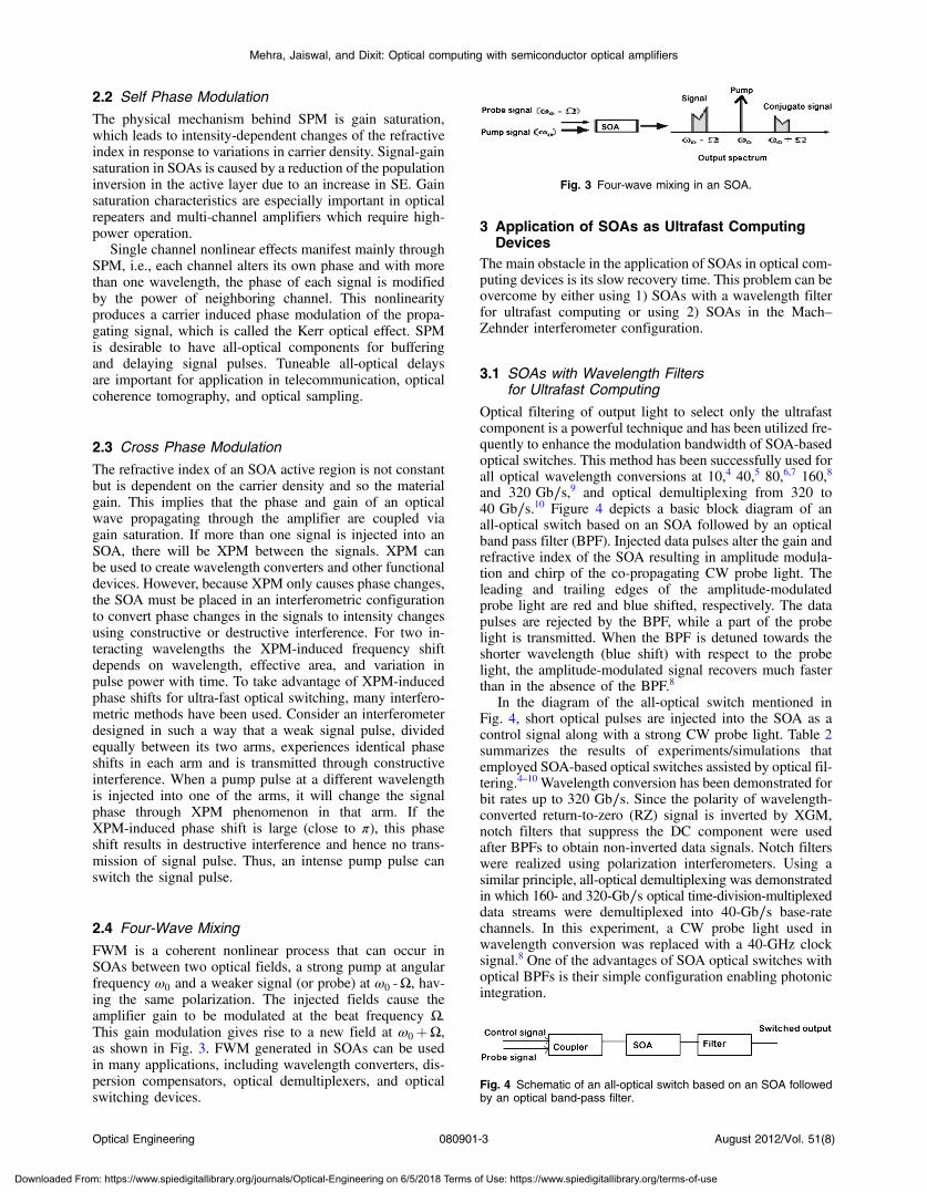
The material gain spectrum of SOAs is homogenously broa-dened, i.e., a change in the carrier density inside the ampli-fier will affect the input signals, so it is possible for a strongsignal at one wavelength to affect the gain of a weak signalat another wavelength. This nonlinear mechanism is calledXGM. The basic XGM is shown in Fig. 2, where a weakcontinuous wave (CW) probe light and a strong pumplight, with a small-signal harmonic modulation at angularfrequency ω, are injected into the SOA. XGM in the ampli-fier will impose the pump modulation on the probe.This means that the amplifier is acting as a wavelengthconverter.3
The information in the pump signal will be transferred tothe probe signal, i.e., the carrier signal and hence it will workas wavelength converter. The most useful figure of merit ofthis converter is the conversion efficiency, defined as theratio between the power of the output probe to the powerof the input pump. The wavelength conversion techni-ques-based SOAs are attractive because of their high-gain,high-saturation output power, wide-gain bandwidth, com-pactness, and integratibility with other photonic devices.The XGM, one of several wavelength conversion techniquesbased on SOAs, is simple to implement and has shown im-pressive operation for a high bit rate. Moreover, the output ofoptical computing devices using XGM in SOA shows insen-sitivity to the polarization of input signals.
Fig. 1 Basic structure of the semiconductor optical amplifier.
Table 1 Characteristics of various SOAs.
MaterialLength(mm)
Current(mA)
Gain(dB)
Nosiefigure(dB)
Saturationpower(dBm)
Bulk 0.9 500 19 7 17
MQW 1.6 500 15 5.7 16.5
Bulk 3 1500 27 7 17
Bulk 1 450 27 5.7 14.7
Fig. 2 Simple wavelength converter using an SOA XGM.
Optical Engineering 080901-2 August 2012/Vol. 51(8)
Mehra, Jaiswal, and Dixit: Optical computing with semiconductor optical amplifiers
Downloaded From: https://www.spiedigitallibrary.org/journals/Optical-Engineering on 6/5/2018 Terms of Use: https://www.spiedigitallibrary.org/terms-of-use
2.2 Self Phase Modulation
The physical mechanism behind SPM is gain saturation,which leads to intensity-dependent changes of the refractiveindex in response to variations in carrier density. Signal-gainsaturation in SOAs is caused by a reduction of the populationinversion in the active layer due to an increase in SE. Gainsaturation characteristics are especially important in opticalrepeaters and multi-channel amplifiers which require high-power operation.
Single channel nonlinear effects manifest mainly throughSPM, i.e., each channel alters its own phase and with morethan one wavelength, the phase of each signal is modifiedby the power of neighboring channel. This nonlinearityproduces a carrier induced phase modulation of the propa-gating signal, which is called the Kerr optical effect. SPMis desirable to have all-optical components for bufferingand delaying signal pulses. Tuneable all-optical delaysare important for application in telecommunication, opticalcoherence tomography, and optical sampling.
2.3 Cross Phase Modulation
The refractive index of an SOA active region is not constantbut is dependent on the carrier density and so the materialgain. This implies that the phase and gain of an opticalwave propagating through the amplifier are coupled viagain saturation. If more than one signal is injected into anSOA, there will be XPM between the signals. XPM canbe used to create wavelength converters and other functionaldevices. However, because XPM only causes phase changes,the SOA must be placed in an interferometric configurationto convert phase changes in the signals to intensity changesusing constructive or destructive interference. For two in-teracting wavelengths the XPM-induced frequency shiftdepends on wavelength, effective area, and variation inpulse power with time. To take advantage of XPM-inducedphase shifts for ultra-fast optical switching, many interfero-metric methods have been used. Consider an interferometerdesigned in such a way that a weak signal pulse, dividedequally between its two arms, experiences identical phaseshifts in each arm and is transmitted through constructiveinterference. When a pump pulse at a different wavelengthis injected into one of the arms, it will change the signalphase through XPM phenomenon in that arm. If theXPM-induced phase shift is large (close to π), this phaseshift results in destructive interference and hence no trans-mission of signal pulse. Thus, an intense pump pulse canswitch the signal pulse.
2.4 Four-Wave Mixing
FWM is a coherent nonlinear process that can occur inSOAs between two optical fields, a strong pump at angularfrequency ω0 and a weaker signal (or probe) at ω0 -Ω, hav-ing the same polarization. The injected fields cause theamplifier gain to be modulated at the beat frequency Ω.This gain modulation gives rise to a new field at ω0 þΩ,as shown in Fig. 3. FWM generated in SOAs can be usedin many applications, including wavelength converters, dis-persion compensators, optical demultiplexers, and opticalswitching devices.
3 Application of SOAs as Ultrafast ComputingDevices
The main obstacle in the application of SOAs in optical com-puting devices is its slow recovery time. This problem can beovercome by either using 1) SOAs with a wavelength filterfor ultrafast computing or using 2) SOAs in the Mach–Zehnder interferometer configuration.
3.1 SOAs with Wavelength Filtersfor Ultrafast Computing
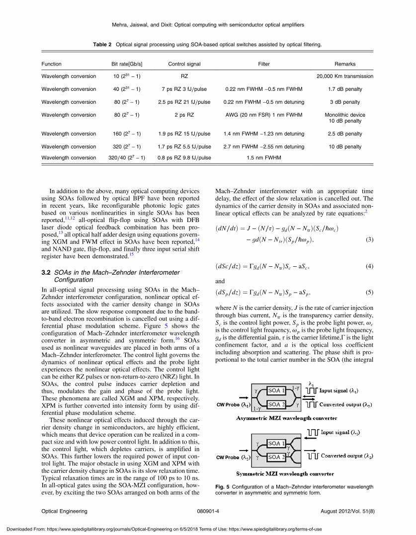
Optical filtering of output light to select only the ultrafastcomponent is a powerful technique and has been utilized fre-quently to enhance the modulation bandwidth of SOA-basedoptical switches. This method has been successfully used forall optical wavelength conversions at 10,4 40,5 80,6,7 160,8
and 320 Gb∕s,9 and optical demultiplexing from 320 to40 Gb∕s.10 Figure 4 depicts a basic block diagram of anall-optical switch based on an SOA followed by an opticalband pass filter (BPF). Injected data pulses alter the gain andrefractive index of the SOA resulting in amplitude modula-tion and chirp of the co-propagating CW probe light. Theleading and trailing edges of the amplitude-modulatedprobe light are red and blue shifted, respectively. The datapulses are rejected by the BPF, while a part of the probelight is transmitted. When the BPF is detuned towards theshorter wavelength (blue shift) with respect to the probelight, the amplitude-modulated signal recovers much fasterthan in the absence of the BPF.8
In the diagram of the all-optical switch mentioned inFig. 4, short optical pulses are injected into the SOA as acontrol signal along with a strong CW probe light. Table 2summarizes the results of experiments/simulations thatemployed SOA-based optical switches assisted by optical fil-tering.4–10 Wavelength conversion has been demonstrated forbit rates up to 320 Gb∕s. Since the polarity of wavelength-converted return-to-zero (RZ) signal is inverted by XGM,notch filters that suppress the DC component were usedafter BPFs to obtain non-inverted data signals. Notch filterswere realized using polarization interferometers. Using asimilar principle, all-optical demultiplexing was demonstratedin which 160- and 320-Gb∕s optical time-division-multiplexeddata streams were demultiplexed into 40-Gb∕s base-ratechannels. In this experiment, a CW probe light used inwavelength conversion was replaced with a 40-GHz clocksignal.8 One of the advantages of SOA optical switches withoptical BPFs is their simple configuration enabling photonicintegration.
Fig. 3 Four-wave mixing in an SOA.
Fig. 4 Schematic of an all-optical switch based on an SOA followedby an optical band-pass filter.
Optical Engineering 080901-3 August 2012/Vol. 51(8)
Mehra, Jaiswal, and Dixit: Optical computing with semiconductor optical amplifiers
Downloaded From: https://www.spiedigitallibrary.org/journals/Optical-Engineering on 6/5/2018 Terms of Use: https://www.spiedigitallibrary.org/terms-of-use
In addition to the above, many optical computing devicesusing SOAs followed by optical BPF have been reportedin recent years, like reconfigurable photonic logic gatesbased on various nonlinearities in single SOAs has beenreported,11,12 all-optical flip-flop using SOAs with DFBlaser diode optical feedback combination has been pro-posed,13 all optical half adder design using equations govern-ing XGM and FWM effect in SOAs have been reported,14
and NAND gate, flip-flop, and finally three input serial shiftregister have been demonstrated.15
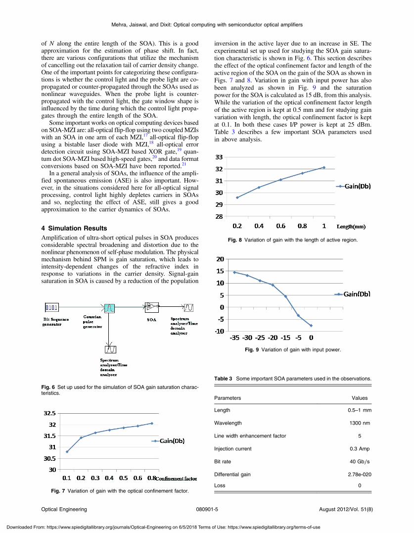
3.2 SOAs in the Mach–Zehnder InterferometerConfiguration
In all-optical signal processing using SOAs in the Mach–Zehnder interferometer configuration, nonlinear optical ef-fects associated with the carrier density change in SOAsare utilized. The slow response component due to the band-to-band electron recombination is cancelled out using a dif-ferential phase modulation scheme. Figure 5 shows theconfiguration of Mach–Zehnder interferometer wavelengthconverter in asymmetric and symmetric form.16 SOAsused as nonlinear waveguides are placed in both arms of aMach–Zehnder interferometer. The control light governs thedynamics of nonlinear optical effects and the probe lightexperiences the nonlinear optical effects. The control lightcan be either RZ pulses or non-return-to-zero (NRZ) light. InSOAs, the control pulse induces carrier depletion andthus, modulates the gain and phase of the probe light.These phenomena are called XGM and XPM, respectively.XPM is further converted into intensity form by using dif-ferential phase modulation scheme.
These nonlinear optical effects induced through the car-rier density change in semiconductors, are highly efficient,which means that device operation can be realized in a com-pact size and with low power control light. In addition to this,the control light, which depletes carriers, is amplified inSOAs. This further lowers the required power of input con-trol light. The major obstacle in using XGM and XPM withthe carrier density change in SOAs is its slow relaxation time.Typical relaxation times are in the range of 100 ps to 10 ns.In all-optical gates using the SOA-MZI configuration, how-ever, by exciting the two SOAs arranged on both arms of the
Mach–Zehnder interferometer with an appropriate timedelay, the effect of the slow relaxation is cancelled out. Thedynamics of the carrier density in SOAs and associated non-linear optical effects can be analyzed by rate equations:2
ðdN∕dtÞ ¼ J − ðN∕τÞ − gdðN − NtrÞðSc∕ℏωcÞ− gdðN − NtrÞðSp∕ℏωpÞ; (3)
ðdSc∕dzÞ ¼ ΓgdðN − NtrÞSc − aSc; (4)
and
ðdSp∕dzÞ ¼ ΓgdðN − NtrÞSp − aSp; (5)
where N is the carrier density, J is the rate of carrier injectionthrough bias current, Ntr is the transparency carrier density,Sc is the control light power, Sp is the probe light power, ωcis the control light frequency, ωp is the probe light frequency,gd is the differential gain, τ is the carrier lifetime,Γ is the lightconfinement factor, and a is the optical loss coefficientincluding absorption and scattering. The phase shift is pro-portional to the total carrier number in the SOA (the integral
Table 2 Optical signal processing using SOA-based optical switches assisted by optical filtering.
Function Bit rate[Gb/s] Control signal Filter Remarks
Wavelength conversion 10 (231 − 1) RZ 20,000 Km transmission
Wavelength conversion 40 (231 − 1) 7 ps RZ 3 fJ∕pulse 0.22 nm FWHM −0.5 nm FWHM 1.7 dB penalty
Wavelength conversion 80 (27 − 1) 2.5 ps RZ 21 fJ∕pulse 0.22 nm FWHM −0.5 nm detuning 3 dB penalty
Wavelength conversion 80 (27 − 1) 2 ps RZ AWG (20 nm FSR) 1 nm FWHM Monolithic device10 dB penalty
Wavelength conversion 160 (27 − 1) 1.9 ps RZ 15 fJ∕pulse 1.4 nm FWHM −1.23 nm detuning 2.5 dB penalty
Wavelength conversion 320 (27 − 1) 1.7 ps RZ 5.5 fJ∕pulse 2.7 nm FWHM −2.55 nm detuning 10 dB penalty
Wavelength conversion 320∕40 (27 − 1) 0.8 ps RZ 9.8 fJ∕pulse 1.5 nm FWHM
Fig. 5 Configuration of a Mach–Zehnder interferometer wavelengthconverter in asymmetric and symmetric form.
Optical Engineering 080901-4 August 2012/Vol. 51(8)
Mehra, Jaiswal, and Dixit: Optical computing with semiconductor optical amplifiers
Downloaded From: https://www.spiedigitallibrary.org/journals/Optical-Engineering on 6/5/2018 Terms of Use: https://www.spiedigitallibrary.org/terms-of-use
of N along the entire length of the SOA). This is a goodapproximation for the estimation of phase shift. In fact,there are various configurations that utilize the mechanismof cancelling out the relaxation tail of carrier density change.One of the important points for categorizing these configura-tions is whether the control light and the probe light are co-propagated or counter-propagated through the SOAs used asnonlinear waveguides. When the probe light is counter-propagated with the control light, the gate window shape isinfluenced by the time during which the control light propa-gates through the entire length of the SOA.
Some important works on optical computing devices basedon SOA-MZI are: all-optical flip-flop using two coupledMZIswith an SOA in one arm of each MZI,17 all-optical flip-flopusing a bistable laser diode with MZI,18 all-optical errordetection circuit using SOA-MZI based XOR gate,19 quan-tum dot SOA-MZI based high-speed gates,20 and data formatconversions based on SOA-MZI have been reported.21
In a general analysis of SOAs, the influence of the ampli-fied spontaneous emission (ASE) is also important. How-ever, in the situations considered here for all-optical signalprocessing, control light highly depletes carriers in SOAsand so, neglecting the effect of ASE, still gives a goodapproximation to the carrier dynamics of SOAs.
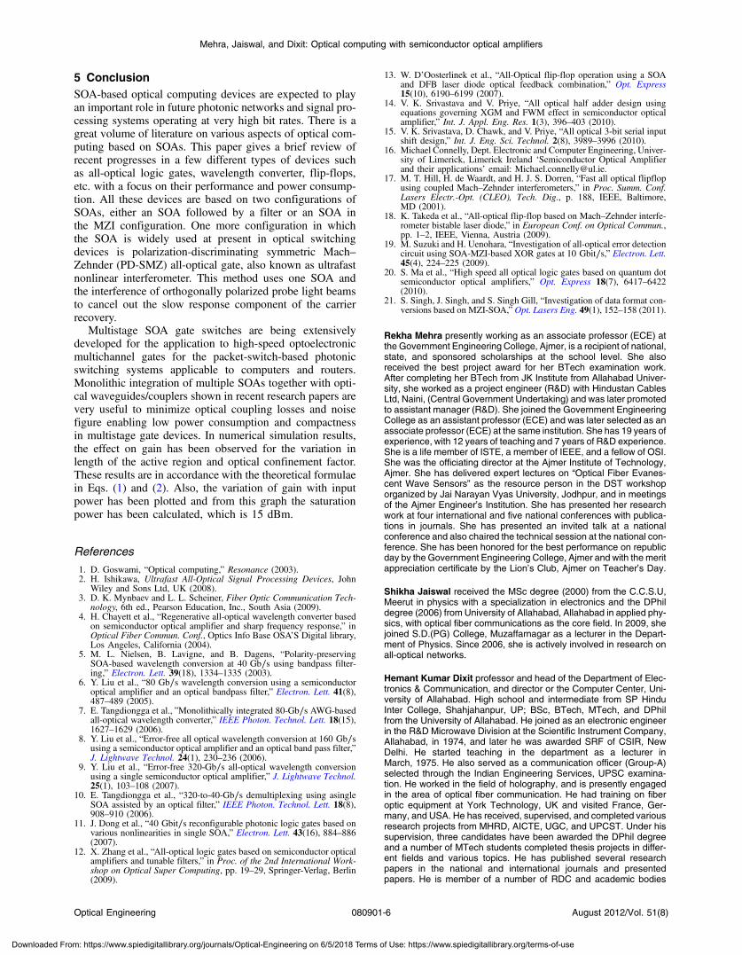
4 Simulation ResultsAmplification of ultra-short optical pulses in SOA producesconsiderable spectral broadening and distortion due to thenonlinear phenomenon of self-phase modulation. The physicalmechanism behind SPM is gain saturation, which leads tointensity-dependent changes of the refractive index inresponse to variations in the carrier density. Signal-gainsaturation in SOA is caused by a reduction of the population
inversion in the active layer due to an increase in SE. Theexperimental set up used for studying the SOA gain satura-tion characteristic is shown in Fig. 6. This section describesthe effect of the optical confinement factor and length of theactive region of the SOA on the gain of the SOA as shown inFigs. 7 and 8. Variation in gain with input power has alsobeen analyzed as shown in Fig. 9 and the saturationpower for the SOA is calculated as 15 dB, from this analysis.While the variation of the optical confinement factor lengthof the active region is kept at 0.5 mm and for studying gainvariation with length, the optical confinement factor is keptat 0.1. In both these cases I/P power is kept at 25 dBm.Table 3 describes a few important SOA parameters usedin above analysis.
Fig. 6 Set up used for the simulation of SOA gain saturation charac-teristics.
Fig. 7 Variation of gain with the optical confinement factor.
Fig. 8 Variation of gain with the length of active region.
Fig. 9 Variation of gain with input power.
Table 3 Some important SOA parameters used in the observations.
Parameters Values
Length 0.5–1 mm
Wavelength 1300 nm
Line width enhancement factor 5
Injection current 0.3 Amp
Bit rate 40 Gb∕s
Differential gain 2.78e-020
Loss 0
Optical Engineering 080901-5 August 2012/Vol. 51(8)
Mehra, Jaiswal, and Dixit: Optical computing with semiconductor optical amplifiers
Downloaded From: https://www.spiedigitallibrary.org/journals/Optical-Engineering on 6/5/2018 Terms of Use: https://www.spiedigitallibrary.org/terms-of-use
5 ConclusionSOA-based optical computing devices are expected to playan important role in future photonic networks and signal pro-cessing systems operating at very high bit rates. There is agreat volume of literature on various aspects of optical com-puting based on SOAs. This paper gives a brief review ofrecent progresses in a few different types of devices suchas all-optical logic gates, wavelength converter, flip-flops,etc. with a focus on their performance and power consump-tion. All these devices are based on two configurations ofSOAs, either an SOA followed by a filter or an SOA inthe MZI configuration. One more configuration in whichthe SOA is widely used at present in optical switchingdevices is polarization-discriminating symmetric Mach–Zehnder (PD-SMZ) all-optical gate, also known as ultrafastnonlinear interferometer. This method uses one SOA andthe interference of orthogonally polarized probe light beamsto cancel out the slow response component of the carrierrecovery.
Multistage SOA gate switches are being extensivelydeveloped for the application to high-speed optoelectronicmultichannel gates for the packet-switch-based photonicswitching systems applicable to computers and routers.Monolithic integration of multiple SOAs together with opti-cal waveguides/couplers shown in recent research papers arevery useful to minimize optical coupling losses and noisefigure enabling low power consumption and compactnessin multistage gate devices. In numerical simulation results,the effect on gain has been observed for the variation inlength of the active region and optical confinement factor.These results are in accordance with the theoretical formulaein Eqs. (1) and (2). Also, the variation of gain with inputpower has been plotted and from this graph the saturationpower has been calculated, which is 15 dBm.
References
1. D. Goswami, “Optical computing,” Resonance (2003).2. H. Ishikawa, Ultrafast All-Optical Signal Processing Devices, John
Wiley and Sons Ltd, UK (2008).3. D. K. Mynbaev and L. L. Scheiner, Fiber Optic Communication Tech-
nology, 6th ed., Pearson Education, Inc., South Asia (2009).4. H. Chayett et al., “Regenerative all-optical wavelength converter based
on semiconductor optical amplifier and sharp frequency response,” inOptical Fiber Commun. Conf., Optics Info Base OSA’S Digital library,Los Angeles, California (2004).
5. M. L. Nielsen, B. Lavigne, and B. Dagens, “Polarity-preservingSOA-based wavelength conversion at 40 Gb∕s using bandpass filter-ing,” Electron. Lett. 39(18), 1334–1335 (2003).
6. Y. Liu et al., “80 Gb∕s wavelength conversion using a semiconductoroptical amplifier and an optical bandpass filter,” Electron. Lett. 41(8),487–489 (2005).
7. E. Tangdiongga et al., ”Monolithically integrated 80-Gb∕s AWG-basedall-optical wavelength converter,” IEEE Photon. Technol. Lett. 18(15),1627–1629 (2006).
8. Y. Liu et al., “Error-free all optical wavelength conversion at 160 Gb∕susing a semiconductor optical amplifier and an optical band pass filter,”J. Lightwave Technol. 24(1), 230–236 (2006).
9. Y. Liu et al., “Error-free 320-Gb∕s all-optical wavelength conversionusing a single semiconductor optical amplifier,” J. Lightwave Technol.25(1), 103–108 (2007).
10. E. Tangdiongga et al., “320-to-40-Gb∕s demultiplexing using asingleSOA assisted by an optical filter,” IEEE Photon. Technol. Lett. 18(8),908–910 (2006).
11. J. Dong et al., “40 Gbit∕s reconfigurable photonic logic gates based onvarious nonlinearities in single SOA,” Electron. Lett. 43(16), 884–886(2007).
12. X. Zhang et al., “All-optical logic gates based on semiconductor opticalamplifiers and tunable filters,” in Proc. of the 2nd International Work-shop on Optical Super Computing, pp. 19–29, Springer-Verlag, Berlin(2009).
13. W. D’Oosterlinek et al., “All-Optical flip-flop operation using a SOAand DFB laser diode optical feedback combination,” Opt. Express15(10), 6190–6199 (2007).
14. V. K. Srivastava and V. Priye, “All optical half adder design usingequations governing XGM and FWM effect in semiconductor opticalamplifier,” Int. J. Appl. Eng. Res. 1(3), 396–403 (2010).
15. V. K. Srivastava, D. Chawk, and V. Priye, “All optical 3-bit serial inputshift design,” Int. J. Eng. Sci. Technol. 2(8), 3989–3996 (2010).
16. Michael Connelly, Dept. Electronic and Computer Engineering, Univer-sity of Limerick, Limerick Ireland ‘Semiconductor Optical Amplifierand their applications’ email: [email protected].
17. M. T. Hill, H. de Waardt, and H. J. S. Dorren, “Fast all optical flipflopusing coupled Mach–Zehnder interferometers,” in Proc. Summ. Conf.Lasers Electr.-Opt. (CLEO), Tech. Dig., p. 188, IEEE, Baltimore,MD (2001).
18. K. Takeda et al., “All-optical flip-flop based on Mach–Zehnder interfe-rometer bistable laser diode,” in European Conf. on Optical Commun.,pp. 1–2, IEEE, Vienna, Austria (2009).
19. M. Suzuki and H. Uenohara, “Investigation of all-optical error detectioncircuit using SOA-MZI-based XOR gates at 10 Gbit∕s,” Electron. Lett.45(4), 224–225 (2009).
20. S. Ma et al., “High speed all optical logic gates based on quantum dotsemiconductor optical amplifiers,” Opt. Express 18(7), 6417–6422(2010).
21. S. Singh, J. Singh, and S. Singh Gill, “Investigation of data format con-versions based on MZI-SOA,” Opt. Lasers Eng. 49(1), 152–158 (2011).
Rekha Mehra presently working as an associate professor (ECE) atthe Government Engineering College, Ajmer, is a recipient of national,state, and sponsored scholarships at the school level. She alsoreceived the best project award for her BTech examination work.After completing her BTech from JK Institute from Allahabad Univer-sity, she worked as a project engineer (R&D) with Hindustan CablesLtd, Naini, (Central Government Undertaking) and was later promotedto assistant manager (R&D). She joined the Government EngineeringCollege as an assistant professor (ECE) and was later selected as anassociate professor (ECE) at the same institution. She has 19 years ofexperience, with 12 years of teaching and 7 years of R&D experience.She is a life member of ISTE, a member of IEEE, and a fellow of OSI.She was the officiating director at the Ajmer Institute of Technology,Ajmer. She has delivered expert lectures on “Optical Fiber Evanes-cent Wave Sensors” as the resource person in the DST workshoporganized by Jai Narayan Vyas University, Jodhpur, and in meetingsof the Ajmer Engineer’s Institution. She has presented her researchwork at four international and five national conferences with publica-tions in journals. She has presented an invited talk at a nationalconference and also chaired the technical session at the national con-ference. She has been honored for the best performance on republicday by the Government Engineering College, Ajmer and with the meritappreciation certificate by the Lion’s Club, Ajmer on Teacher’s Day.
Shikha Jaiswal received the MSc degree (2000) from the C.C.S.U,Meerut in physics with a specialization in electronics and the DPhildegree (2006) from University of Allahabad, Allahabad in applied phy-sics, with optical fiber communications as the core field. In 2009, shejoined S.D.(PG) College, Muzaffarnagar as a lecturer in the Depart-ment of Physics. Since 2006, she is actively involved in research onall-optical networks.
Hemant Kumar Dixit professor and head of the Department of Elec-tronics & Communication, and director or the Computer Center, Uni-versity of Allahabad. High school and intermediate from SP HinduInter College, Shahjahanpur, UP; BSc, BTech, MTech, and DPhilfrom the University of Allahabad. He joined as an electronic engineerin the R&D Microwave Division at the Scientific Instrument Company,Allahabad, in 1974, and later he was awarded SRF of CSIR, NewDelhi. He started teaching in the department as a lecturer inMarch, 1975. He also served as a communication officer (Group-A)selected through the Indian Engineering Services, UPSC examina-tion. He worked in the field of holography, and is presently engagedin the area of optical fiber communication. He had training on fiberoptic equipment at York Technology, UK and visited France, Ger-many, and USA. He has received, supervised, and completed variousresearch projects from MHRD, AICTE, UGC, and UPCST. Under hissupervision, three candidates have been awarded the DPhil degreeand a number of MTech students completed thesis projects in differ-ent fields and various topics. He has published several researchpapers in the national and international journals and presentedpapers. He is member of a number of RDC and academic bodies
Optical Engineering 080901-6 August 2012/Vol. 51(8)
Mehra, Jaiswal, and Dixit: Optical computing with semiconductor optical amplifiers
Downloaded From: https://www.spiedigitallibrary.org/journals/Optical-Engineering on 6/5/2018 Terms of Use: https://www.spiedigitallibrary.org/terms-of-use

of other universities and institutions, and a life member and fellow inorganizations like ISTE, IETE, etc. He organized, participated, andchaired a number of symposiums, workshops and conferences. Inthe University, he has worked at various posts, such as a memberof the Administrative Computer Center, OSD examinations, assistantproctor, assistant dean student welfare, Dy. director PG admissions,
member core committee UG admissions, etc. He has been the jointsecretary, Allahabad University Teacher’s Association; social secre-tary of the Diamond Jubilee Hostel; superintendent of the Dr. TaraChand Hostel; and is presently serving as the warden of the DiamondJubilee Hostel, at the University of Allahabad. He also served astreasurer, secretary to IETE, Allahabad.
Optical Engineering 080901-7 August 2012/Vol. 51(8)
Mehra, Jaiswal, and Dixit: Optical computing with semiconductor optical amplifiers
Downloaded From: https://www.spiedigitallibrary.org/journals/Optical-Engineering on 6/5/2018 Terms of Use: https://www.spiedigitallibrary.org/terms-of-use