strained-layer ingaas(p) quantum well semiconductor … bound... · semiconductor lasers and...
TRANSCRIPT
by P.I.A. THIJS, L.F. TIEMEIJER, I.I.M. BINSMAand T. VAN DONGEN
Philips J. Res. 49 (1995) 187-224
STRAINED-LAYER InGaAs(P) QUANTUM WELLSEMICONDUCTOR LASERS AND SEMICONDUCTOR
LASER AMPLIFIERS
Philips Optoelectronics Centre, Prof Holstlaan 4, 5656 AA Eindhoven, The Netherlands
AbstractProgress in long-wavelength strained (compressive and tensile) InGaAs(P)quantum well semiconductor lasers and amplifiers for applications inoptical fibre communication systems is reviewed. By the application ofgrown-in strain, device performance is considerably improved to such anextent that conventional bulk and unstrained quantum well active-layerdevices are outperformed, while high reliability, similar to that ofunstrained devices, is maintained.
Keywords: III-V semiconductor; optoelectronics; semiconductor laser;MOVPE; quantum well; polarization; laser amplifier.
PhlUps Journal of Research Vol. 49 No. 3 1995 187
1. Introduetion
Strained-layer quantum well (QW) semiconductor lasers were fabricated forthe first time [1]by adding indium to GaAs active layers in order to bridge the880 to 1100nm wavelength gap left by the lower and higher wavelength limitsof AI GaAsjGaAs and InGaAsPjlnP, respectively. The research was extendedto the other group III - V material systems after theoretical predictions ofimproved performance for QW semiconductor lasers with the active materialdeliberately grown in a state of compressive strain [2-4]. In 1989, the firstsuccessful application of compressive strain in 1.5JLm wavelength lno.sGao.2AsjInGaAsP MQW semiconductor lasers was reported by a group in the PhilipsOptoelectronics Centre [5]. To date, enhanced and reliable performance ofstrained-layer QW semiconductor lasers has been reported for InGaAs(P)jInPand AIGalnAsjlnP telecommunication lasers, AIGalnPjGaAs visible-lightemitting lasers, and AIGa(In)As(P)jGaAs near-infrared emitting lasers. The
P.J.A. Thijs et al.
dramatic impact of strained-layer QWs is best illustrated by the fact that theyare now commercially available.
In this paper, we review the progress in strained-layer InP-based semicon-ductor lasers and semiconductor laser amplifiers for applications in opticalfibre communication systems. In Section 2, the effect of the strain on theband structure and the impact on the semiconductor laser performance willbe reported briefly. Some design considerations for enhanced performanceInP-based strained-layer telecommunication lasers and the ensuing fabricationprocedures of device structures will be given in Section 3. In Section 4, we willcompare the experimental data with the theoretical predictions and interpretthe observed data on the basis of the strain-induced band structure modifica-tions. Section 5 reports on the reliability of high-power strained-layer MQWlasers. In addition, strain compensation, achieved by employing structureswith alternating compressively and tensile strained layers, is demonstratedto be a useful tool to enhance the performance and reliability of devicesemploying a large number of strained-layer QWs. The latest developmentsin strained-layer MQW semiconductor laser amplifiers, amongst others thoseemploying tensile and compressively strained QWs in one single active layer toeliminate their polarization dependence, are reviewed in Section 6. Finally, inSection 7, we summarize some conclusions of this paper.
2. Effects of strain on the band structure and consequences for laser performance
The band structure of bulk III - V compound semiconductors is character-ized by a conduction band with light effective mass, a degenerate valenceband at the zone centre with heavy effective mass at bandgap energy Eg,and a spin split-off (so) valence band at energy Eg + Äso. This asymmetrieband structure is far from optimal for low-threshold laser operation.Especially in 1.5/-Lm wavelength InGaAsP, the complex valence subbandstructure facilitates appreciable non-radiative recombinations through Augerprocesses [6-8] and intervalenee band absorption [9-11] in which the heavy-hole (hh) and spin split-off valence subbands are involved in most cases. InAuger processes, the excess energy of the electron-hole recombination istransferred to another carrier (electron or hole), which becomes excited to ahigher-energy state in the band. As a result, both the threshold current andits temperature sensitivity increase, whereas the reabsorption of bandgapphotons by intervalenee band absorption increases the threshold currentbut, more seriously, degrades the differential efficiency.
Reshaping ofthe band structure to a higher symmetry by growing the activematerial lattice-mismatched to the substrate was proposed to enhance the
188 PhIlips Journal of Research Vol.4)1 No. 3 1995
Quantum well lasers
performance [2-4]. For layers below the critical thickness [12], the resultingbiaxial in-plane strain causes tetragonal deformation of the cubic symmetryofthe crystallattice. This modifies mainly the valence subband structure whilethe conduction band, due to its spherical s-like character, is hardly affected.For growth on (001) substrates, a simple strain tensor is obtained, with theonly non-vanishing components given by
(1)
andC12
Ezz = E_L= -2-cEll'11(2)
where x,y are taken within, and z perpendicular to the growth plane, as and aeare the relaxed lattice parameters of the substrate and of the epitaxial layer,respectively, and Cij are components of the elastic stiffness tensor. For ae > as,i.e., Ell< 0, the epitaxial layer is under biaxial compressive strain, whereasfor ae < as the strain is tensile. The total strain can be resolved into a purelyhydrostatic (hy) component given by
flVEhy=V = Exx + Eyy + Ezz = 2EII+ E_L
and a purely axial (ax) component given by
(3)
(4)
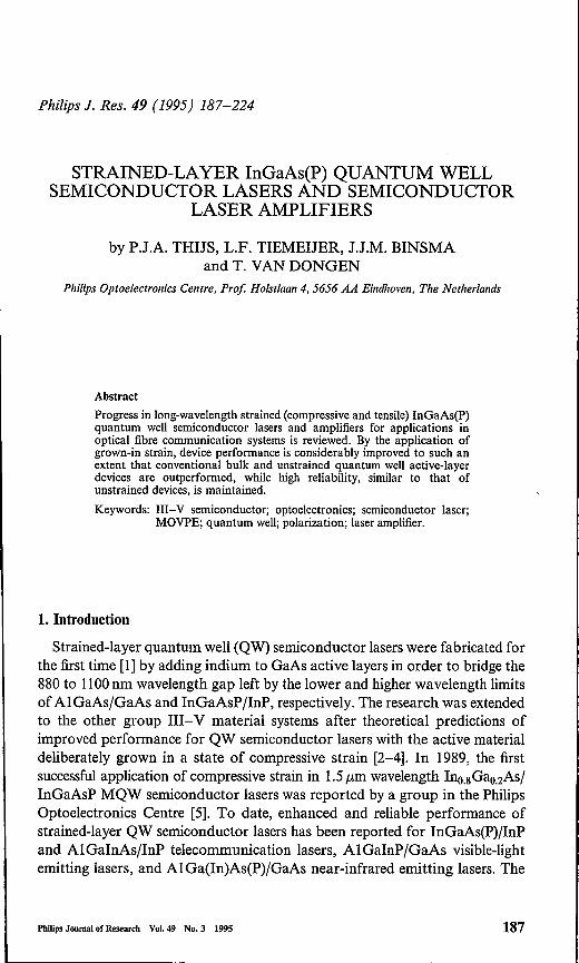
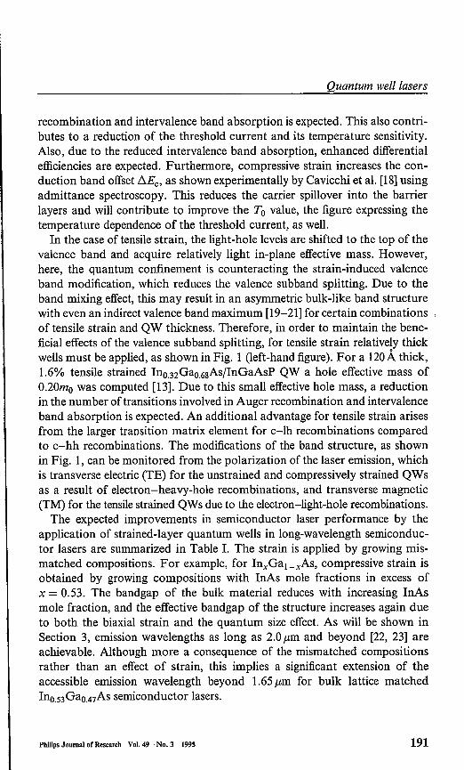
The hydrostatic component affects only the bandgap. The more importanteffects for semiconductor lasers, however, arise from the axial component,splitting the light-hole (lh) and heavy-hole states at the k = 0 point. Forcompressive strain, the hh levels are brought on top of the valence band,and the in-plane effective mass is reduced. Tensile strain brings the lh levelson top of the valence band, which also have a small in-plane effective mass.The quantum size effect, introduced necessarily due to the limited thicknessfor coherent growth of defect-free layers, enhances the valence subbandsplitting in case of compressive strain. This effect is illustrated in Fig. 1, whichcompares the band structures oflattice matched InO.53Ga0.47As/lnGaAsPand1.2% biaxially compressed Ino.7Gao.3As/lnGaAsP in the middle and right-handfigures, respectively, computed using an eight-band Kane-type k.p Hamiltonian[13]. The dramatically increased valence sub band separation eliminates theband mixing and results in a large reduction of the hole effective mass from0.70mo for the unstrained QW to 0.I5mo for the 1.2% compressively strainedQW. From a simple QW model, the modal gain per quantum well from the
Philips Journalof Research Vol. 49 No. 3 1995 189
P.J.A. Thijs et al.
o1.6% Tens. (x=0.32)
Lz= 120A
s -50Ql
É.w
-100
0.05 0.10
LM (x=0.53)Lz= 80A
1.2% Compr. (x=0.7)Lz= 25A
~,''''ih-''''''''',..., ," ", ,, ,, ,
KI! (2n/ao)Fig. I. Calculated band structure of 1.6% tensile strained (x = 0.32), lattice matched (x = 0.53)and 1.2% compressively strained InxGal_x As/lnGaAsP in left, middle and right figures, respec-tively. The well width L, is chosen for emission at 1.5/lm wavelength. The solid and dashed linesdenote the hh and lh subbands, respectively. The wavevector is taken along [210] which is inter-mediate between [lOO]and [110]; the [OOI]is assumed to be perpendicular to the plane ofthe well.
lowest-energy subband transition can be derived as [14]
where me and my are the electron and hole effective masses. For a nearlysymmetric band structure, the transparency carrier density per quantum wellcan be expressed as Ntr ex:y'(memy) [4]. Consequently, the differential gain isgiven by
dgmax dg ~--rv-ex:dNtr dN m; +me
From these expressions, it is seen that the transparency and threshold currentsare reduced, and that the differential gain increases with decreasing hole effec-tive mass. For equal electron and hole effective masses the differential gain ismaximum. The increased differential gain is expected to reduce the linewidthenhancement factor (aH ex:Ij(dgjdN)) [15,16], and to increase the relaxationoscillation frequency u; ex:(dgjdN)) [16, 17].Additionally, since the carriersare confined to smaller values of the k-vector in the case of strained-layerQWs, a large reduction in the number of transitions involved in Auger
190
(5)
(6)
Philips Journalof Research Vol.49 No.3 1995
Quantum wel/lasers
recombination and intervalenee band absorption is expected. This also contri-butes to a reduction of the threshold current and its temperature sensitivity.Also, due to the reduced intervalenee band absorption, enhanced differentialefficiencies are expected. Furthermore, compressive strain increases the con-duction band offset !lEe, as shown experimentally by Cavicchi et al. [18] usingadmittance spectroscopy. This reduces the carrier spillover into the barrierlayers and will contribute to improve the To value, the figure expressing thetemperature dependence of the threshold current, as well.
In the case of tensile strain, the light-hole levels are shifted to the top of thevalence band and acquire relatively light in-plane effective mass. However,here, the quantum confinement is counteracting the strain-induced valenceband modification, which reduces the valence subband splitting. Due to theband mixing effect, this may result in an asymmetrie bulk-like band structurewith even an indirect valence band maximum [19-21] for certain combinationsof tensile strain and QW thickness. Therefore, in order to maintain the bene-ficial effects of the valence subband splitting, for tensile strain relatively thickwells must be applied, as shown in Fig. 1 (left-hand figure). For a 120A thick,1.6% tensile strained Ino.32Gao.6sAsjInGaAsP QW a hole effective mass ofO.20mo was computed [13]. Due to this small effective hole mass, a reductionin the number of transitions involved in Auger recombination and intervaleneeband absorption is expected. An additional advantage for tensile strain arisesfrom the larger transition matrix element for c-Ih recombinations comparedto c-hh recombinations. The modifications of the band structure, as shownin Fig. 1, can be monitored from the polarization of the laser emission, whichis transverse electric (TE) for the unstrained and compressively strained QWsas a result of electron-heavy-hole recombinations, and transverse magnetic(TM) for the tensile strained QWs due to the electron-light-hole recombinations.
The expected improvements in semiconductor laser performance by theapplication of strained-layer quantum wells in long-wavelength semiconduc-tor lasers are summarized in Table 1. The strain is applied by growing mis-matched compositions. For example, for InxGa'_xAs, compressive strain isobtained by growing compositions with InAs mole fractions in excess ofx = 0.53. The band gap of the bulk material reduces with increasing InAsmole fraction, and the effective bandgap of the structure increases again dueto both the biaxial strain and the quantum size effect. As will be shown inSection 3, emission wavelengths as long as 2.0/.Lm and beyond [22, 23] areachievable. Although more a consequence of the mismatched compositionsrather than an effect of strain, this implies a significant extension of theaccessible emission wavelength beyond 1.65/.Lm for bulk lattice matchedIno.53Gao.47As semiconductor lasers.
Philips Journalof Research Vol. 49 .No. 3 1995 191
P.J.A. Thijs et al.
TABLE ISummary of the effects of biaxial strain on the performance of long wave-length quantum well lasers (Jth is the threshold current density, dG/dN isthe differential gain, Ir is the relaxation oscillation frequency, aH is thelinewidth enhancement factor, To is the characteristic temperature, ai is the
internalloss, and 'Tlis the differential efficiency).
Effect of biaxial strain Effect on laser parameter
Reduction of hole effective massReduction of Auger recombinationReduction of intervalenee band absorptionValence band maximum (hh or lh)Compression: increased b..EcAccessible bandgap extended
Jth ~,dG/dN /"fr /" aH -,
To/'ai~,'Tl/'TE or TM polarizationTo /"Jth -,
À up to 2.0/-Lm
3. Design of long wavelength strained-layer MQW lasers and device structures
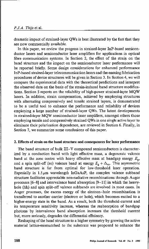
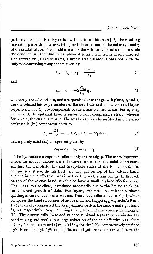
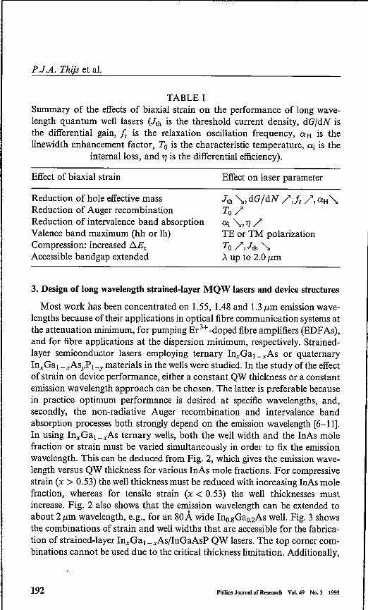
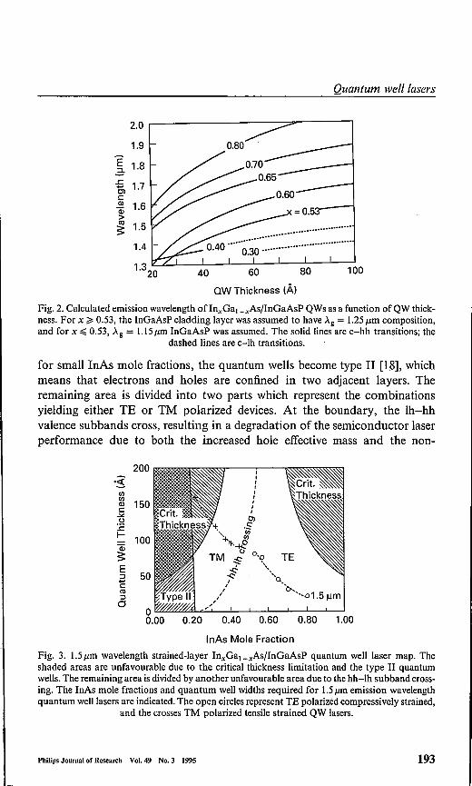
Most work has been concentrated on 1.55, 1.48 and 1.3 usx: emission wave-lengths because oftheir applications in optical fibre communication systems atthe attenuation minimum, for pumping Er3+ -doped fibre amplifiers (EDFAs),and for fibre applications at the dispersion minimum, respectively. Strained-layer semiconductor lasers employing ternary InxGal_xAs or quaternaryInxGal_xAsyPI_y materials in the wells were studied. In the study ofthe effectof strain on device performance, either a constant QW thickness or a constantemission wavelength approach can be chosen. The latter is preferable becausein practice optimum performance is desired at specific wavelengths, and,secondly, the non-radiative Auger recombination and intervalenee bandabsorption processes both strongly depend on the emission wavelength [6-11].In using InxGal_xAs ternary wells, both the well width and the InAs molefraction or strain must be varied simultaneously in order to fix the emissionwavelength. This can be deduced from Fig. 2, which gives the emission wave-length versus QW thickness for various InAs mole fractions. For compressivestrain (x > 0.53) the well thickness must be reduced with increasing InAs molefraction, whereas for tensile strain (x < 0.53) the well thicknesses mustincrease. Fig. 2 also shows that the emission wavelength can be extended toabout 2/-Lm wavelength, e.g., for an 80Á wide Ino.sGao.2As well. Fig. 3 showsthe combinations of strain and well widths that are accessible for the fabrica-tion of strained-layer In.Ga, _xAs/lnGaAsP QW lasers. The top corner com-binations cannot be used due to the critical thickness limitation. Additionally,
192 Philips Journal of Research Vol.49 No.3 .1995
Quantum weil lasers
2.0
1.9
Ê 1.8.3-.J:: 1.7-ClCID 1.6a;>co 1.5S
1.4
QW Thickness (Ál
Fig. 2. Calculated emission wavelength ofInxGal_xAs/InGaAsP QWs as a function ofQW thick-ness. For x;;;' 0.53, the InGaAsP cladding layer was assumed to have >'g = 1.25J.Lm composition,and for x ::;;; 0.53, À g = 1.15J.Lm InGaAsP was assumed. The solid lines are c-hh transitions; the
dashed lines are c-lh transitions.
Philips Journol of Research Vol. 49 No. 3 1995 193
for small InAs mole fractions, the quantum wells become type Ir [18], whichmeans that electrons and holes are confined in two adjacent layers. Theremaining area is divided into two parts which represent the combinationsyielding either TE or TM polarized devices. At the boundary, the lh-hhvalence subbands cross, resulting in a degradation of the semiconductor laserperformance due to both the increased hole effective mass and the non-
200
50
.~(J)
:ll 150c-'".s.J::l-a;SE:J-Cco:Jo
100
InAs Mole Fraction
Fig. 3. 1.5J.Lm wavelength strained-layer InxGal_xAs/InGaAsP quantum well laser map. Theshaded areas are unfavourable due to the critical thickness limitation and the type II quantumwells. The remaining area is divided by another unfavourable area due to the hh-lh sub band cross-ing. The InAs mole fractions and quantum well widths required for 1.5JLm emission wavelengthquantum weil lasers are indicated. The open circles represent TE polarizéd compressively strained,
and the crosses TM polarized tensile strained QW lasers.
P.J.A. Thijs et al.
radiative recombinations. The dashed line represents the required well widthsand InAs mole fractions in the InxGal_xAs quantum wells for 1.5I'm wave-length lasers [25].
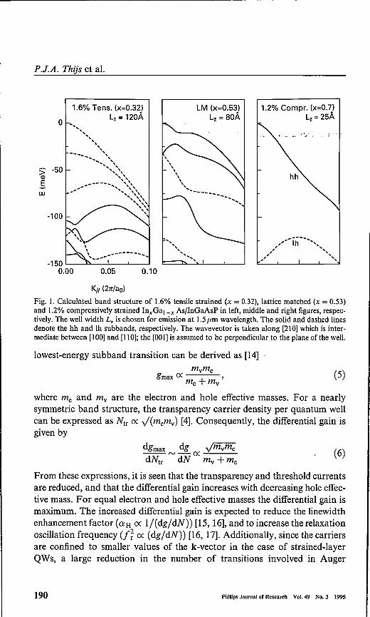
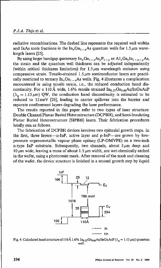
By using larger bandgap quaternary InxGal_xAsyPl_ y or AlxGayInl_x_ yAs,the strain and the quantum well thickness can be adjusted independently(within critical thickness limitation) for 1.5J.Lm wavelength emission usingcompressive strain. Tensile-strained 1.5 J.Lm semiconductor lasers are practi-cally restricted to ternary InxGal_xAs wells. Fig. 4 illustrates a complicationencountered in using tensile strain, i.e., the reduced conduction band dis-continuity. For a 1l0Ä wide, 1.6% tensile strained In0.32GaO.6SAs/InGaAsP(Àg = 1.15 J.Lm) QW, the conduction band discontinuity is estimated to bereduced to l2meV [26], leading to carrier spillover into the barrier andseparate confinement layers degrading the laser performance.The results reported in this paper refer to two types of laser structure:
Double Channel Planar Buried Heterostructure (DCPBH), and Semi-InsulatingPlanar Buried Heterostructure (SIPBH) lasers. Their fabrication proceduresbriefly run as follows.The fabrication of DCPBH devices involves two epitaxial growth steps. In
the first, three layers-n-InP, active layer and p-InP-are grown by low-pressure organometallic vapour phase epitaxy (LP-OMVPE) on a two-inchn-type InP substrate. Subsequently, two channels, about 3 J.Lm deep and10 J.Lm wide, leaving a mesa of about 1.5 J.Lm width, are wet-chemically etchedin the wafer, using a photoresist mask. After removal of the mask and cleaningof the wafer, the device structure is finished in a second growth step by liquid
Ec
InP
799 meV
106
------ Ih-- hh
Fig. 4. Calculated band structure of 110Ä 1.6% Ino.32Gao.6sAsjlnGaAsP (Àg = 1.15tIm) quantumwell.
194 Philip. Journal or Research Vol.49 No.3 1995
Quantum wel! lasers
phase epitaxy (LPE), allowing for maskless selective growth of epitaxiallayerswhile embedding the mesa with p-type and n-type InP current blocking layersrespectively. The third and fourth steps, the p-InP confinement and p+ -InGa-As(P) contact layers respectively, are grown on the entire wafer for planariza-tion. After the growth, the wafer is thinned to about lOOpsi: and both sides ofthe structure are metallized and alloyed. Laser chips are cleaved and mountedp-side down on either copper heatsinks on TO-5 headers or on silicon heat-sinks on carriers.
The SIPBH lasers [34-36] are fabricated entirely by LP-OMVPE in threegrowth steps. In the first, three layers-n-InP, active layer, and p-InP-aregrown successively on a two-inch n-type InP substrate. Then, using an Si02mask, all grown layers are wet-chemically etched away, except for a mesa,about 1 to 2 pm wide and 2 to 3 usx: high, which becomes the active stripe.With the Si02 mask still on top of the mesa, a semi-insulating Fe-doped InPlayer (p = 108n·cm) and an n-InP layer are grown selectively. After removalofthe mask, p-InP and p+ -InGaAs layers are grown on the entire wafer in thethird LP-OMVPE growth. The wafers are processed using metallization andmounting procedures similar to the DCPBH laser.
4. Device characteristics
4.1. Threshold current density versus strain
The effect of strain on the threshold current density of 1.5 J.Lm wavelengthInxGal_xAsjInGaAsP SQW lasers was systematically studied for the firsttime by the Philips group [25]. The strain was varied from 2.1% tension(x = 0.22, L, = l60A) to 1.8% compression (x = 0.80, Lz = 20A). Forboth signs ofthe strain, reductions in threshold current density were observed,with a minimum as low as 92 Ajcm2 for 1.1 cm cavity length 1.6% tensilestrained InO.32GaO.68As SQW lasers [25, 37]. For compressively strainedSQW lasers, minimum threshold current densities around 140 to 160Ajcm2
were observed for devices ranging from 4.5 to 3.5 mm in length. The thresholdcurrent densities were observed to decrease monotonically up to large cavitylengths, which demonstrates that in strained-layer lasers the threshold currentdensity is loss-limited rather than transparency-limited [41].
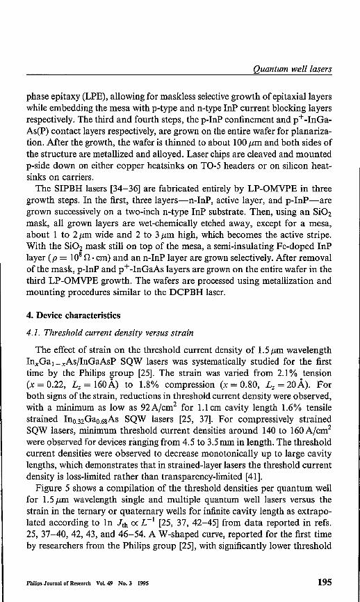
Figure 5 shows a compilation of the threshold densities per quantum wellfor 1.5 J.Lm wavelength single and multiple quantum well lasers versus thestrain in the ternary or quaternary wells for infinite cavity length as extrapo-lated according to In Jth exL-1 [25, 37, 42-45] from data reported in refs.25, 37-40, 42, 43, and 46-54. A W-shaped curve, reported for the first timeby researchers from the Philips group [25], with significantly lower threshold
Philips Jouroal of Research Vol. 49 No. 3 1995 195
P.J.A. Thijs et al.
current densities for strained than for unstrained QW lasers, is obtained. Thesetwo branches can be explained as follows.
4.1.1. Compressive strain branch
With increasing compressive strain, the hole effective mass monotonicallydecreases and the hh-Jh valence subband splitting increases. Both effectscontribute to the observed reduction in the threshold current density. However,for large compressive strain, the ternary InxGal_xAs wellwidths must be grownvery.narrow in order to maintain the emission around 1.5/-Lm wavelength, asindicated in Fig. 3. Although the modal gain was theoretically predicted to beindependent of the quantum well width [52], in practice, for narrow wells,interwell-width variations and decreased current injection efficiencies [55]broaden and reduce the gain. Consequently, a larger carrier density in thewell is required, which additionally enhances the Auger recombination andexplains the slight increase in threshold current density observed in Fig. 5for compressively strained ternary wellswith Ell > 1.5%. An increase in thresh-old current density due to crystalline defects can be excluded, since the wellsare narrower than the critical thickness [12], as indicated in Fig. 3. For1.5pm wavelength InxGal_xAs quantum weIl lasers, the optimum compres-sive strain is around 1%. By applying larger bandgap strained-layer InGaAsPquaternary material, the quantum well width may be increased for I.S/-Lmwavelength emission. It is expected and indeed demonstrated [40, 46] thatthe increase in threshold current density observed for narrow, highly strainedInxGal_xAs QW lasers is reduced.
196 Philips Journal of Research, Vol.49 No.3 1995
Lz (ternary) (Ä)
200 100 70 45 20N 600
l>. ternary OWE
~500 l>. + quat.OW
8 40011
...J 300'lij
~ 200~#
l>..... l>.Q) 100 l>. *,1 +c.-5-, 0-3. -2 -1 0 2
Tension _ Strain (%) __ Compression
Fig. 5. Summary of threshold current densities per QW deduced for infinite cavity length 1.5J.Lmlasers versus the strain in the InGaAs(p) QWs, using data reported in [25, 37-40,42,43,46-54].
The solid lines represent fits through the data points.
Quantum weil lasers
4.1.2. Tensile strain branch
Figure 5 shows the second branch, with also a significant reduction of thethreshold current density for tensile strain. This was originally not predictedtheoretically, but could be readily explained [13, 56] after the experimentaldemonstration. In the region of the lh-hh valence subband crossing, i.e., fortensile strains up to about 0.9%, band mixing effects increase the in-planehole effective mass. For certain combinations of tensile strain and quantumwell width, the band structure even becomes indirect [19-21]. -The resultingheavy-hole mass increases both the threshold current and the non-radiativelosses such that it prevents up to 2mm cavity length 0.3,0.6 and 0.9% tensilestrained InxGal_xAs SQW lasers from lasing at room temperature in our case[25, 37]. So far, low threshold current lasers with strains in the quantum wellsranging from zero to about 1% tension have not been reported, in agreementwith our observations. For larger tensile strains, the light-hole states form thevalence band maximum as confirmed by the TM polarization of the laseremission. With further increases of both the tensile strain and the quantumwell width, the 1h-hh valence subband separation increases, which reducesthe band mixing effects, resulting in decreased hole effective mass and non-radiative loss. Consequently, with increasing strain the threshold currentdensity dramatically decreases to a minimum value as low as 88A/cm2obtained for 1.6% tensile strained Ino.32Gao.6sAsSQW lasers.For larger strains, an abrupt increase in threshold current density is
observed. For the 2.1% tensile strained SQW laser, this can be ascribed totwo effects. Firstly, this structure has a large well width grown under strain(160Á x 2.1% strain). This is above the critical thickness, and indicationsfor misfit dislocations were obtained from Nomarski interference contrastmicroscopy and high-resolution X-ray diffraction measurements. Secondly,taking into account the band structure for a 110Á wide 1.6% tensile strainedIno.32Gao.6sAs/InGaAsP (Àg = 1.15f..Lm) well, as shown in Fig. 4, the conduc-tion band offset in this 2.1% tensile strained SQW structure will be smaller ormay be even a type 11band structure.
Philips Journalof Research Vol. 49 No. 3 1995 197
4.2. Effect of strain on the threshold current density: hole effective mass or non-radiative recombination?
The significant reductions in the threshold current densities observed inFig. 5 may be explained by both the reduced hole effective mass and/or non-radiative losses such as Auger recombination and intervalenee band absorp-tion. In order to gain more insight into the origin of these improvements,we studied the threshold current density as a function of temperature.
P.J.A. Thijs et al.
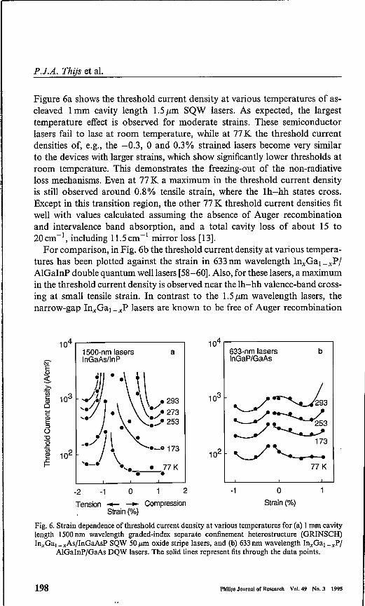
Figure 6a shows the threshold current density at various temperatures of as-cleaved 1mm cavity length 1.5 J.Lm SQW lasers. As expected, the largesttemperature effect is observed for moderate strains. These semiconductorlasers fail to lase at room temperature, while at 77K the threshold currentdensities of, e.g., the -0.3, 0 and 0.3% strained lasers become very similarto the devices with larger strains, which show significantly lower thresholds atroom temperature. This demonstrates the freezing-out of the non-radiativeloss mechanisms. Even at 77K a maximum in the threshold current densityis still observed around 0.8% tensile strain, where the lh-hh states cross.Except in this transition region, the other 77 K threshold current densities fitwell with values calculated assuming the absence of Auger recombinationand intervalenee band absorption, and a total cavity loss of about 15 to20cm-1, including 11.5cm-1 mirrorloss [13].
For comparison, in Fig. 6b the threshold current density at various tempera-tures has been plotted against the strain in 633 nm wavelength InxGal_xPjAIGaInP double quantum welliasers [58-60]. Also, for these lasers, a maximumin the threshold current density is observed near the lh-hh valence-band cross-ing at small tensile strain. In contrast to the 1.5J.Lm wavelength lasers, thenarrow-gap InxGal_xP lasers are known to be free of Auger recombination
Tension _ ...._ CompressionStrain (%)
Fig. 6. Strain dependence of threshold current density at various temperatures for (a) 1mm cavitylength 1500nm wavelength graded-index separate confinement heterostructure (GRINSCH)InxGal_xAs/InGaAsP SQW 50Mmoxide stripe lasers, and (b) 633nm wavelength InxGal_xP/
AlGalnP/GaAs DQW lasers. The solid lines represent fits through the data points.
104.-----------,1500-nm lasers aInGaAslinP
-2 -1 o
198
104,------------,633-nm lasers bInGaP/GaAs
~~93
3~'173
~~77K
2 -1 oStrain (%)
Philip. Journal of Research Vol. 49 No. 3 1995
Philip. Journalof Research Vol. 49 No. 3 1995 199
Quantum wel/lasers
and intervalenee band absorption. This is confirmed by an almost constanttemperature dependence of threshold current density, independently of diestrain, and indicates that in these lasers the strain-induced modification ofthe effective mass is the dominant effect. The ratios of the 293 and 77K thresh-old current densities are about ten. Similar ratios for the 1500nm SQW lasersare only observed for the largest strains (~1 % compression, and ~ 1.6% ten-sion), indicating that, in these cases, the non-radiative losses have beenreduced to a large extent.
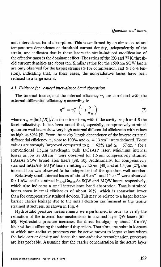
4.3. Evidence for reduced intervalenee band absorption
The internal loss ai and the internal efficiency 'fJi are correlated with theexternal differential efficiency ït according to
'fJ-I = 'fJjl (1 + :~ ) (7)
where am = [ln(l/ R)l! L is the mirror loss, with L the cavity length and R thefacet reflectivity. It has been noted that, especially, compressively strainedquantum welliasers show very high external differential efficiencieswith valuesas high as 80% [5]. From the cavity length dependence of the inverse externaldifferential efficiency, 'fJi close to 100% and ai = 13cm-I were deduced. Thesevalues are strongly improved compared to ïls = 62% and ai = 67cm-I for aconventional 1.5 J.Lm wavelength bulk InGaAsP laser. Minimum internallosses as low as 3.8 cm-I were observed for 1.5 J.Lm compressively strainedInGaAs SQW broad area lasers [38, 50]. Additionally, for compressivelystrained InGaAsP MQW lasers emitting at 1.5Mm[40] and at 1.3 J.Lm [27], theinternalloss was observed to be independent of the quantum well number.
Relatively small internallosses of about 9cm-I and 11cm-I were observedfor 1.6% tensile strained Ino.32Gao.6sAsSQW and MQW lasers, respectively,which also indicates a small intervalenee band absorption. Tensile strainedlasers show internal efficiencies of about 70%, which is somewhat lowerthan for compressively strained devices. This may be related to a larger hetero-barrier carrier leakage due to the small electron confinement in the tensilestrained structures, as shown in Fig. 4.Hydrostatic pressure measurements were performed in order to verify the
reduction of the internalloss mechanisms in strained-layer QW lasers [61-63]. Hydrostatic pressure increases the direct bandgap by about 10meV/kbar without affecting the subband dispersion. Therefore, the point in k-spaceat which non-radiative processes can be active moves to larger values wherethe hole carrier density and hence the non-radiative recombination processesare less probable. Assuming that the carrier concentration in the active layer
P.J.A. Thijs et al.
is pinned at threshold, Auger recombination has no effect on the differentialefficiency. So changes in 1J are primarily due to the variations in intervaleneeband absorption. These changes can be carefully controlled by the hydrostaticpressure and their magnitude provides a measure of the strength of inter-valence band absorption.
By comparison, measurements were made under the same conditions onbulk InGaAsP DH, unstrained Ino.53Gao.47As, 1.8% compressively strainedInO.8GaO.2As, and on 1.6% tensile strained Ino.32GaO.68As MQW devices [64,65]. All devices operated at 1.5 f.1.m wavelength. Figure 7 shows the normalized1J against the hydrostatic pressure, where a reduction in intervalenee bandabsorption becomes evident from improvements in the differential efficiency.As can be seen, there is a dramatic increase in 1J for the bulk InGaAsP andthe unstrained MQW devices. By contrast, for the first time, almost no changesin 1J with pressure were observed in both the 1.6% tensile and 1.8% compres-sively strained quantum weIl lasers. This may be interpreted by assuming thatmodification of the valence band structure by the grown-in strain has alreadyremoved intervalenee band absorption, and hence the application of hydro-static pressure is ineffective. Additionally, studies performed independentlyby Fuchs et al. [66] demonstrate the insensitivity of the absorption on thehole density in compressively strained 1.5 f.1.m wavelength InxGal_xAs/InGaAsP QW lasers. This also leads to the conclusion that intervaleneeband absorption has become negligible.
2.50
>-0 2.00c:Oli3:Ew'0 1.50Ol.!a(ijEC5 1.00z
0.500
+
3 42
o
5 6
Hydrostatlc Pressure (kbar)
Fig. 7. Normalized efficiency against hydrostatic pressure for (+) bulk InGaAsP, (Ll) unstrainedIno.s3Gao.47AsflnGaAsP, (0) 1.8% compressively strained Ino.sGao.2AsflnGaAsP, and (e) 1.6%
tensile strained Ino.32Gao.6sAsflnGaAsP MQW lasers operating at 1.5 pm wavelength.
200 PhiUps Journal of Research Vol.49 No.3 1995
Quantum wel! lasers
4.3. Temperature dependence of the threshold current and high temperaturecharacteristics
The temperature dependence of the threshold current is commonlyexpressed by a characteristic temperature To given by
1 dTo = dT [In Jth] (8)
Typical values of To for InGaAsP lasers are about 50K. Initial expectations,led by the reduction of the Auger recombination by the application of strain,ran high where values as high as 140K were predicted [67]. However, a simpleanalysis [68] shows that incomplete removal ofthe Auger recombination limitsthe maximum achievable To to about 100K. Ignoring the weakly temperaturedependent trap- and surface-mediated non-radiative recombination [69], thethreshold current can be expressed as
Jth ex: B(T)N~h + CAR(T)N~h (9)
where B(T)N~h is the bi-molecular radiative recombination current JR with Bthe radiative recombination coefficient, and CAR(T)N~h the current JAR dueto three-carrier non-radiative Auger processes with CAR(T) the Auger coeffi-cient. For an ideal quantum welliaser, B(T) ex: T-1 and Nth ex: T. For thisanalysis, however, we assume Nth ex: Tl+x(x~O), where x accounts for anynon-ideality factors such as carriers occupying higher subbands, carrier spill-over into the barrier material, or intervalenee band absorption, which all mayincrease the temperature sensitivity of the threshold carrier density beyondlinearity. The Auger coefficient is exponentially temperature-activated, withan activation energy b..E determined by the band structure. Combining theserelations, the value of To can be written as
T(I + J;RR)To = ( b..E) J
1+ 2x + 3 + 3x + kT ;RR(10)
Philip. Journalof Research Vol. 49 No. 3 1995 201
In the ideal case, i.e., hR/ JR = 0, b..E = 0 and x = 0, a To value of 300 K isexpected around room temperature. For GaAsjAlGaAs [70] and InGaAsjGaAs [60] MQW lasers, To values close to this prediction were indeedreported. If JAR» JR, a maximum To value of lOOK around roomtemperature may be expected, and if x and b..E #- 0, the To value becomeseven smaller.
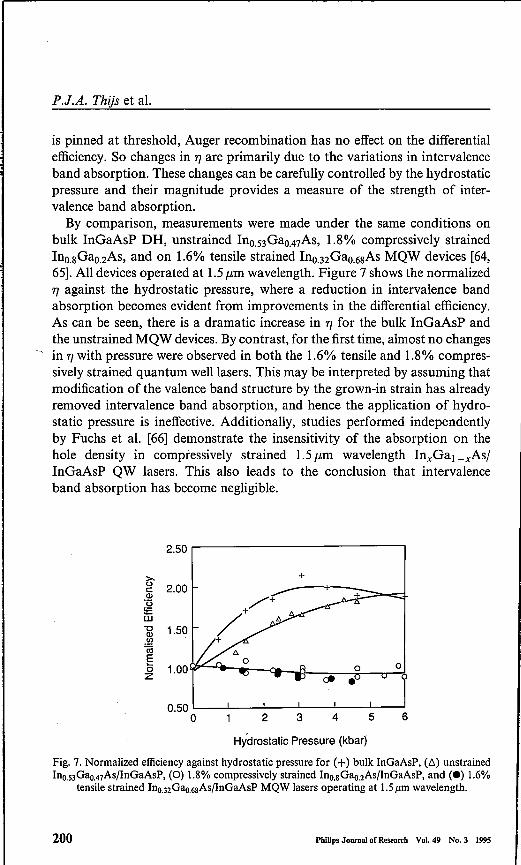
Figure 8 gives a summary of To values for 1.5pm wavelength strained-layerSQW and 4QW lasers versus the strain, Data represented by the hour-glass
P.J.A. Thijs et al.
100,-------------------------------~X----------~EEl GRINSCHSQW(77Ks T s 300K) ,11-------.• GRINSCH- 4QW(300K~T ~ 330K) '(i"X literaturereports X +/90
80
g700
I-
60
50
40-3 -2
Tension ..,__-1 0 2
Strain(%) -- Compression
Fig. 8. To values of 1.5pm wavelength lasers versus the strain in the InxGal_xAs quantum wells:(Efl) InxGal_xAs/InGaAsP SQW lasers, 77~T~300K; (+) InxGal_xAs/InGaAsP 4QW lasers,293 ~ T ~323K; (X) literature reports for devices employing SQW and MQW active layers withvarious cavity lengths and device structures by Alcatel, AT&T, Bellcore, BNR, BTRL, NEe,
NTT, Philips and University of Southern California researchers.
symbols are literature reports and show a wide scatter because the To valueswere deduced over various temperature ranges from devices with differentlateral current confinement structures, quantum well numbers and cavitylengths. Our data, deduced from SQW and 4QW lasers with an identical devicestructure and cavity length, are accentuated by the solid and dashed lines as aguide to the eye, respectively. We observe minimum To values for unstrainedQW lasers and improved values for both signs ofthe strain, indicating that theAuger recombination is indeed reduced in strained-layer MQW lasers. Figure8 also shows that no To values over 100K have been reported, supporting thearguments given above.
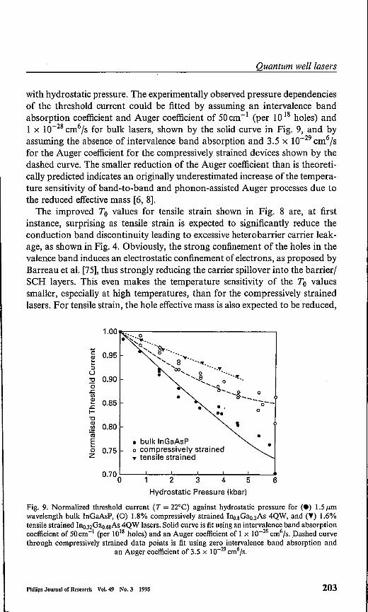
Reduction in Auger recombination in 1.5/-Lm wavelength strained-layerMQW lasers was also indicated by studies of the hydrostatic pressuredependence of the threshold current. In a loss-free laser, one would expectthe threshold current to increase with.pressure as the bandgap increases [61].This has indeed .been observed for GaAs lasers [61]. By contrast, all 1.5/-Lmwavelength devices studied show a decrease in threshold current withincreasing pressure, as shown in Fig. 9. The reductions are smallest for thestrained-layer devices. This indicates that the non-radiative current was alreadyreduced in the strained MQW devices, and hence less reduction is observed
202 Phlllps Journal of Research Vol.49 No.3 1995
Quantum weil lasers
with hydrostatic pressure. The experimentally observed pressure dependenciesof the threshold current could be fitted by assuming an intervalenee bandabsorption coefficient and Auger coefficient of 50cm-I (per 1018 holes) and1 x 10-28 cm6/s for bulk lasers, shown by the solid curve in Fig. 9, and byassuming the absence of intervalenee band absorption and 3.5 x 10⁻²⁹ cm6/sfor the Auger coefficient for the compressively strained devices shown by thedashed curve. The smaller reduction of the Auger coefficient than is theoreti-cally predicted indicates an originally underestimated increase ofthe tempera-ture sensitivity of band-to-band and phonon-assisted Auger processes due tothe reduced effectivemass [6, 8].The improved To values for tensile strain shown in Fig. 8 are, at first
instance, surprising as tensile strain is expected to significantly reduce theconduction band discontinuity leading to excessive heterobarrier carrier leak-age, as shown in Fig. 4. Obviously, the strong confinement of the holes in thevalence band induces an electrostatic confinement of electrons, as proposed byBarreau et al. [75],thus strongly reducing the carrier spillover into the barrier/SeR layers. This even makes the temperature sensitivity of the To valuessmaller, especially at high temperatures, than for the compressively strainedlasers. For tensile strain, the hole effective mass is also expected to be reduced,
1.00 .... 0.~..:.~ ..0. ~.
-, tf'· ............ 8 ." ...
-, '00 y
..................g :( ..........0
........00__ .....& 0
---è--
0.700L---'---2.l---.....I3---'-4-----'5-- ..6
Hydrostatic Pressure (kbar)
Fig. 9. Normalized threshold current (T = 22°C) against hydrostatic pressure for (.) 1.5/Lmwavelength bulk InGaAsP, (0) 1.8% compressively strained Ino.8Gao.2As4QW, and (T) 1.6%tensile strained Ino.32Gao.68As4QW lasers. Solid curve is fit using an intervalenee band absorptioncoefficient of 50 cm-1 (per 1018 holes) and an Auger coefficient of I x 10-28cm6/s. Dashed curvethrough compressively strained data points is fit using zero intervalenee band absorption and
an Auger coefficient of 3.5 x 10⁻²⁹cm6/s.
ë 0.95~::JUJ:! 0.90os:Ul
~s:I-
0.85
"0
.~ 0.80ca
E~ 0.75
Philips Journalof Research Vol. 49 No. 3 1995
•• ..
•• ,• bulk InGaAsPo compressively strained'" tensile strained
o
••
203
P.J.A. Thijs et al.
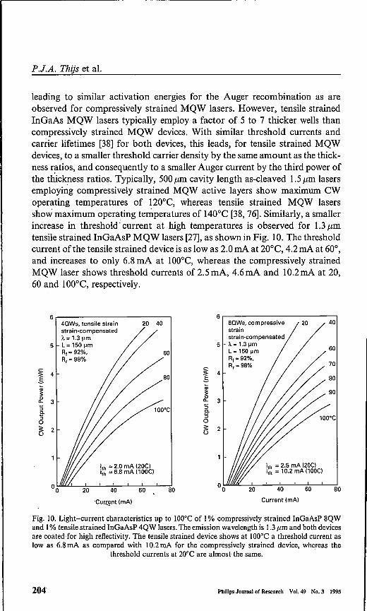
leading to similar activation energies for the Auger recombination as areobserved for compressively strained MQW lasers. However, tensile strainedInGaAs MQW lasers typically employ a factor of 5 to 7 thicker wells thancompressively strained MQW devices. With similar threshold currents andcarder lifetimes [38] for both devices, this leads, for tensile strained MQWdevices, to a smaller threshold carrier density by the same amount as the thick-ness ratios, and consequently to a smaller Auger current by the third power ofthe thickness ratios. Typically, 500 pm cavity length as-cleaved 1.5 pm lasersemploying compressively strained MQW active layers show maximum ewoperating temperatures of 1200e, whereas tensile strained MQW lasersshow maximum operating temperatures of 1400e [38, 76]. Similarly, a smallerincrease in threshold' current at high temperatures is observed for 1.3 J.Lmtensile strained InGaAsP MQW lasers [27], as shown in Fig. 10. The thresholdcurrent ofthe tensile strained device is as low as 2.0mA at 200e, 4.2mA at 60°,and increases to only 6.8 mA at 1000e, whereas the compressively strainedMQW laser shows threshold currents of 2.5 mA, 4.6 mA and 10.2 mA at 20,60 and 1000e, respectively.
40Ws, tensile strainstrain-compensatedÀ= 1.31Jm
5 L=1501JmRf=92%,R,=98%
20 40 80Ws, compressivestrainstrain-compensated
5 À=1.3IJmL=150lJmRf=92%,R,= 98%
§' 4É
~CL 3:::JB-:::Jos: 2u
6r---------------------~
i1h = 2_0mA (20C)i1h = 6_8mA (100C)
i1h = 2.5 mA (20C)i1h = 10_2mA (100C)
§' 4É
~oCL 3'5B-:::Jo~ 2
20 40
-Cur.Qlnt (mA)
80 60 8060 40
Current (mA)
Fig. 10. Light-current characteristics up to 1000e of 1% compressively strained InGaAsP 8QWand 1% tensile strained InGaAsP 4QW lasers. The emission wavelength is 1_3J.Lm and both devicesare coatedfor high reflectivity. The tensile strained device shows at 1000e a threshold current aslow as 6.8mA as compared with 10_2mA for the compressively strained device, whereas the
threshold currents at 200e are almost the same.
204 Philip. Journalof Research Vol. 49 No. 3 1995
Quantum wel/lasers
Philips Journalof Research Vol. 49 No. 3 1995 205
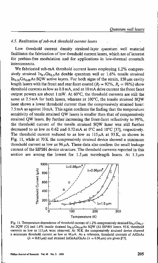
4.5. Realization of sub-mA threshold current lasers
Low threshold current density strained-layer quantum well materialfacilitates the fabrication of low threshold current lasers, which are of interestfor prebias-free modulation and for applications in lo~-thermal crosstalkinterconnects ..We fabricated sub-mA threshold 'current lasers employing 1.2% compres-
sively strained Ino.7Gao.3Asdouble quantum well or 1.6% tensile strainedIno.32Gao.6sAsSQW active layers. For both signs of the strain, 150/-Lm cavitylength lasers with the front and rear facet coated (Rf = 92%, R; = 98%) showthreshold currents as low as 0.8mA, and at 10mA drive current the front facetoutput powers are about 1mW. At 60°C, the threshold currents are still thesame at 2.5 mA for both lasers, whereas at lOOoe, the tensile strained SQWlaser shows a lower threshold current than the compressively strained laser:7.5mA as against 10mA. This again confirms the finding that the temperaturesensitivity of tensile strained QW lasers is smaller than that of compressivelystrained QW lasers. By further increasing the front-facet reflectivity to 9?%,the threshold current of the tensile strained SQW laser was still furtherdecreased to as low as 0.62 and 0.72mA at ooe and lOoe [37], respectively.The threshold current reduced to as low as 115/-LA at 93K, as shown inFig. 11, while at 70K the compressively strained device showed a minimumthreshold current as low as 96/-LA. These data also confirm the small leakagecurrent of the SIPBH device structure. The threshold currents reported in thissection are among the lowest for 1.5/-Lm wavelength lasers. At 1.3/-Lm
«:::l. 800
200 300Temperature (Kl
Fig. I I. Temperature dependence of threshold current of 1.2% compressively strained Ino.7Gao.3-As 2QW (0) and 1.6% tensile strained Ino.32Gao.6sAsSQW (t» SIPBH lasers. 93K thresholdcurrents as low as 115JlA were observed. At 70K the compressively strained device showeda minimum threshold current as low as 96 JlA. As a reference, threshold currents of AIGaAs
(A = 0.85Jlm) and strained InGaAsjGaAs (A = 0.96Jlm) are given [77].
P.J.A. Thijs et al.
wavelength, a minimum threshold current of 1.3mA was obtained for acompressively strained InGaAsP SQW laser [28].
4.6. Linewidth enhancement factor
The linewidth enhancement factor aH is a key parameter that determinesthe spectral properties of semiconductor lasers and semiconductor laser ampli-fiers under modulation. It characterizes the spectrallinewidth D..v ~ (1+ a~)[81], and the frequency chirp .6.vChirp ~ .J(1 + a~) [82] due to fluctuations inthe carrier density altering the refractive index. Both effects are highly undesir-able in 1.5pm lasers used in dispersive long-distance communication systemsbecause they limit the data transmission capacity. The linewidth enhancementfactor is defined as the ratio of the variation in refractive index n with thecarrier density N to the variation in optical gain g with the carrier density by
-41fdnjdNaH = >'dgjdN
where>. is the wavelength ofthe light. The contributions to the refractive indexvariations are: a) the anomalous dispersion due to band-to-band electronictransitions, b) the plasma term due to the free-carrier plasma effect, and c)the thermal contribution. We will demonstrate experimentally the strain andstructural effects of the plasma term on the linewidth enhancement factor[83],and show that this confirms the positive expectations for strained devices.Experimentally determined linewidth enhancement factors of 1.5p,m lasers
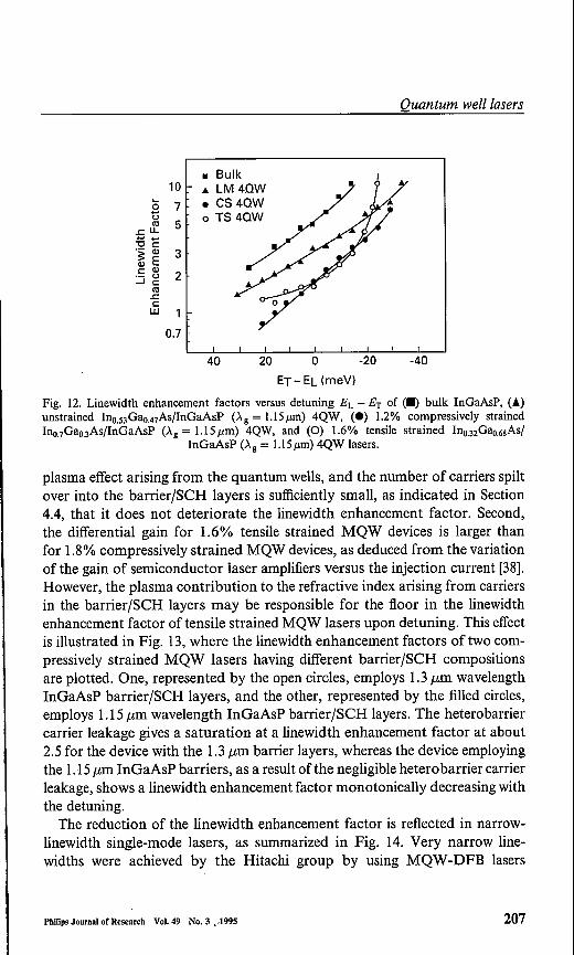
are plotted in Fig. 12versus the detuning, i.e., the transition photon energy ETminus the bandgap photon energy EL' At the gain peak wavelength, i.e.,ET - EL = 0, linewidth enhancement factors as low as 1.7 for compressivelystrained MQW, and even as low as 1.5 for tensile strained MQW lasers, wereobserved. This is a significant improvement over unstrained Ino.53Gao.47AsMQW and bulk InGaAsP lasers showing aH parameters of 3 and 5, respec-tively. As indicated in Fig. 12, a further reduction of the linewidth enhance-ment factor can be obtained by increasing the wavelength detuning topositive ET - EL values, as is possible in distributed feedback lasers. A line-width enhancement factor as low as 0.8 is deduced for compressively strainedMQW lasers at 20meV detuning. Reduced linewidth enhancement factors forcompressively strained MQW lasers were confirmed at 1.5 usx: [85-87] and alsoat 1.3p,mwavelength [28, 88].At the gain peak wavelength, the linewidth enhancement factor of the tensile
strained MQW lasers is smaller than that ofthe compressively strained devices(1.5 as against 1.7, as shown in Fig. 12).Two causes can be mentioned for thiseffect. First, in the tensile strained MQW laser there is no contribution of the
(11)
206 Philips Journal of Research Vol.49 No.3 1995
Quantum weil lasers
• Bulk10 ... LM 4QW
....7 • CS 4QW0.... o TS 4QWo
Cl) 5.eLL........"'0 c:.- Ol 3~ Ec Ol 2.- tJ_, c:
Cl).ec:w
0.7
20 o -2040 -40
ET-EL (meV)
Fig. 12. Linewidth enhancement factors versus detuning EL - ET of (.) bulk InGaAsP, (.)unstrained Ino.s3Gao.47As/lnGaAsP (>'g = 1.15JLm)4QW, (.) 1.2% compressively strainedInO.7GaO.3As/lnGaAsP (>'g = 1.l5JLm) 4QW, and (0) 1.6% tensile strained InO.32GaO.6SAs/
InGaAsP (>'g = 1.15JLm) 4QW lasers.
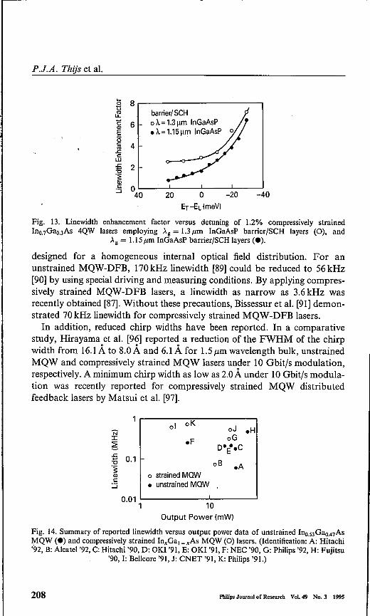
plasma effect arising from the quantum wells, and the number of carriers spiltover into the barrier/SCH layers is sufficiently small, as indicated in Section4.4, that it does not deteriorate the linewidth enhancement factor. Second,the differential gain for 1.6% tensile strained MQW devices is larger thanfor 1.8% compressively strained MQW devices, as deduced from the variationof the gain of semiconductor laser amplifiers versus the injection current [38].However, the plasma contribution to the refractive index arising from carriersin the barrier/SCl-l layers may be responsible for the floor in the linewidthenhancement factor oftensile strained MQW lasers upon detuning. This effectis illustrated in Fig. 13, where the linewidth enhancement factors oftwo com-pressively strained MQW lasers having different barrier/SCH compositionsare plotted. One, represented by the open circles, employs 1.3 usx: wavelengthInGaAsP barrier/SCl-l layers, and the other, represented by the filled circles,employs 1.15 /km wavelength InGaAsP barrier/SCl-l layers. The heterobarriercarrier leakage gives a saturation at a linewidth enhancement factor at about2.5 for the device with the 1.3 /km barrier layers, whereas the device employingthe 1.15 /km InGaAsP barriers, as a result of the negligible hetero barrier carrierleakage, shows a linewidth enhancement factor monotonically decreasing withthe detuning.
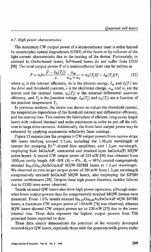
The reduction of the linewidth enhancement factor is reflected in narrow-linewidth single-mode lasers, as summarized in Fig. 14. Very narrow line-widths were achieved by the Hitachi group by using MQW-DFB lasers
Philip. Journal of Research Vol. 49 No. 3 •,1995 207
P.J.A. Thijs et al. .
~ 8.--------------,~ barrier/ SCH5l 6 0 À.= 1.31lm InGaAsP~ • À.= 1.151lm InGaAsP 0tJ
ffi 4s:c:UJ
:§ 2.~c::::; OL--~----~----~----~
40 20 0 -20 -40Er-EL(meV)
Fig. 13. Linewidth enhancement factor versus detuning of 1.2% compressively strainedIno.7Gao.3As 4QW lasers employing >'g = J.3 Jl-m InGaAsP barrier/SCH layers (0), and
>'g = 1.15 Jl-m InGaAsP barrier/SCH layers (.).
designed for a homogeneous internal optical field distribution. For anunstrained MQW-DFB, 170kHz linewidth [89] could be reduced to 56 kHz[90] by using special driving and measuring conditions. By applying compres-sively strained MQW-DFB lasers, a linewidth as narrow as 3.6 kHz wasrecently obtained [87].Without these precautions, Bissessur et al. [91]demon-strated 70kHz linewidth for compressively strained MQW-DFB lasers.
In addition, reduced chirp widths have been reported. In a comparativestudy, Hirayama et al. [96] reported a reduction of the FWHM of the chirpwidth from 16.1Á to 8.0Á and 6.1Á for 1.5 f.Lm wavelength bulk, unstrainedMQW and compressively strained MQW lasers under 10 Gbitfs modulation,respectively. A minimum chirp width as low as 2.0Á under 10 Gbitfs modula-tion was recently reported for compressively strained MQW distributedfeedback lasers by Matsui et al. [97].
ol oKoJN .H
:c .F oG2 O·E··Cs:+J 0.1 oB"0 .A.§Ol o strained MQWc
• unstrained MQW::J
0.011 10
Output Power (mW)
Fig. 14. Summary of reported linewidth versus output power data of unstrained InO.53Ga0.47AsMQW (.) and compressively strained InxGal_xAs MQW (0) lasers. (Identification: A: Hitachi'92, B: AJcatel '92, C: Hitachi '90, D: OKI '91, E: OKI '91, F: NEC '90, G: Philips '92, H: Fujitsu
'90, I: Bellcore '91, J: CNET '91, K: Philips '91.)
208 Phlllps Journal of Research Vol. 49 No. 3 1995
Quantum weil lasers
4.7. High power characteristics
The maximum CW output power of a semiconductor laser is either limitedby catastrophic optical degradation (COD) of the facets or by roll-over of thelight-current characteristic due to the heating of the device. Fortunately, incontrast to GaAs-based lasers, InP-based lasers do not suffer from COD[98].The total output power P of a semiconductor laser can be written as
[I - Ith(1j)] amP = 'fJihv = 'fJd(1j)[I - Ith(1j)] Yj (12)
e am +ai
where ïti is the internal efficiency, hu is the photon energy, Im and ~(T) arethe drive and threshold currents, e is the electronic charge, am and ai are themirror and the internal losses, 'fJd(1j) is the external differential quantumefficiency, and Yj is the junction voltage. Ith(1j) and 'fJd(1j) are a function ofthe junction temperature 1j.In previous sections, the strain was shown to reduce the threshold current,
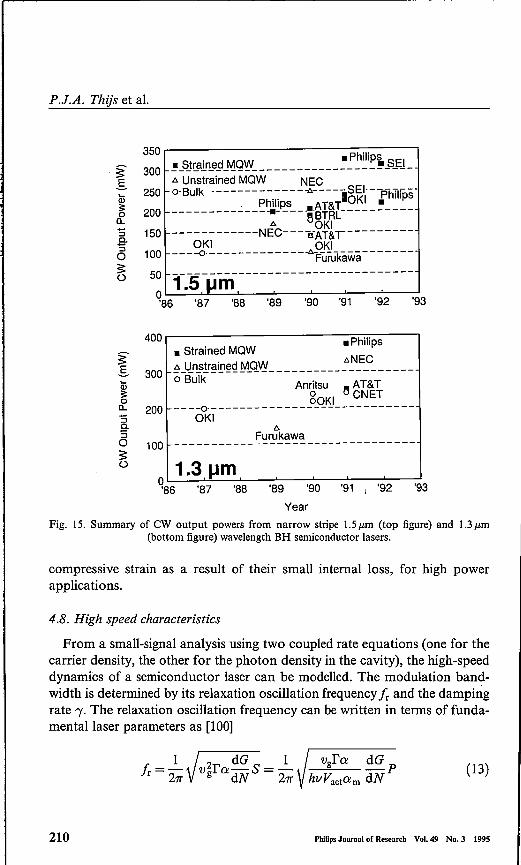
the temperature dependence ofthe threshold current and differential efficiency,and the internalloss. This enables the fabrication of efficient, long cavity lengthlasers with reduced thermal and series resistances in order to put off the roll-over to large drive currents. Additionally, the front facet output power may beenhanced by applying asymmetrie reflectivity facet coatings.Figure 15 summarizes the progress in CW output powers from narrow stripe
BH lasers emitting around 1.5Mm, including the 1.48J.Lm wavelength ofinterest for pumping Er3+ -doped fibre amplifiers, and 1.3Mm wavelength,employing bulk InGaAsP, unstrained and strained-layer InGaAs(p) MQWactive layers. A record CW output power of 325mW [38]was obtained from1000Mmcavity length AR-HR (Rf = 4%, R, = 98%) coated compressivelystrained InO.7GaO.3AsjlnGaAsP MQW-SIPBH lasers at 1.5Mmwavelength.We observed an even larger output power of 380mW from 1.3Mmwavelengthcompressively strained InGaAsP MQW lasers, also employing the SIPBHcurrent confinement [28]. Despite these high power densities, sudden failuresdue to COD were never observed.Tensile strained QW lasers also show high power operation, although some-
what lower output powers than for compressively strained MQW devicesweremeasured. From 1.6% tensile strained InO.32GaO.6SAsjlnGaAsP4QW SIPBHlasers, a maximum CW output power of l50mW [76]was observed, whereasSQW lasers showed CW output powers up to 220mW [37] due to the lowerinternal loss. These data represent the highest output powers from TMpolarized lasers reported to date.These data clearly demonstrate the potentialof the recently developed
strained-layer QW lasers, especially those with the quantum wells grown under
Philip. Journal of Research Vol; 49 No. 3 1995 209
P.J.A. Thijs et al.
350§' 300§. 250Qjs: 2000a..'S 150c.'S 1000$: 50o
. • Philips SEI!_SJ@l~e9_~Q~ ! _!>.UnstrainedMOW NEGo-Bulk ---------------1::.----- SEI---phTljps
. Philips AT&T10KI•- - - - - - - - - - - - - -:-- - - -~-~k~L-- - - - - - - --------------NEC---nAT&i---------
OKI OKI----o·--------------!>.-FurukaiNa-------
1~1)-~iTï------------------------O~~~~~--~--~--~--~--_='86 '87 '88 '89 '90 '91 '92 '93
400r------------------------.~P~h~iIi~pS~---,• StrainedMOW
!>.NEG~_~n~tr~~~Q~_q~ _o Bulk300
!>.Furukawa
100
Anritsu 13AT&TgOKI GNET----~----------------------------
OKI200
1.3 IJmOL_--~--~--~--~--~--~--_='86 '87 '88 '89 '90 '91 I '92 '93Year
Fig. 15. Summary of CW output powers from narrow stripe 1.5 tLm (top figure) and 1.3 tLm(bottom figure) wavelength BH semiconductor lasers.
1Ir =--211" (13)
compressive strain as a result of their small internal loss, for high powerapplications.
4.8. High speed characteristics
From a small-signal analysis using two coupled rate equations (one for thecarrier density, the other for the photon density in the cavity), the high-speeddynamics of a semiconductor laser can be modelled. The modulation band-width is determined by its relaxation oscillation frequency Ir and the dampingrate /. The relaxation oscillation frequency can be written in terms of fund a-ment al laser parameters as [100]
210 PblUpsJournal of Research Vol. 49 No. 3 1995
2 1'Y = Kir +-
Ts(14)
Quantum wel! lasers
where Vg is the group velocity in the cavity, a is the total cavity loss, r is theoptical confinement factor, dG/ dN is the differential gain, S is the photon den-sity in the cavity, hu is the photon energy, Vact is the active layer volume, am isthe mirror loss, and P is the emitted optical output power. Above threshold,where the photon density in the cavity exceeds the spontaneous emissioncoupled into the optical mode, the damping rate "y due to the nonlinear gainis correlated withfr according to [100]
where Ts is the carrier lifetime. The maximum possible intrinsic - 3dBmodulation bandwidth is determined solely by the K factor, according to
(15)
In the series of devices employing bulk, unstrained MQW, and strained-layerMQW active layers, the differential gain and the optical output power areboth increased, as shown in the preceding sections, while the reduced I'for QWs can be compensated for by increasing their number. For maximumJr, also, the active layer volume should be minimized, which implies inpractice that the cavity length is short. A large number of quantum wellsin the active layer is then beneficial to overcome the large mirror losses.Theoretically, intrinsic -3dB bandwidths as large as 90 GHz for compressivelystrained InxGa'_xAs/InP MQW lasers were predicted [16, 17].Table 11summarizes the record -3dB bandwidths at the operating currents
given within brackets, and the estimated intrinsic -3dB bandwidths. Thistable shows that the largest bandwidths, despite the improvements, are stillfar behind the theoretical predictions. In addition, most bandwidths wererealized at impractically large drive currents for optical communication systemapplications using FP lasers. We achieved 19GHz bandwidth for a DFB atlow drive current [94]. It has been recognized that the photon density in thecavity reduces the differential gain, especially for strained MQW lasers.Equation (13) then gives a too optimistic result. The physical origins of thegain saturation factor have been attributed to various phenomena such ascavity standing wave dielectric gratings [106], spectral hole burning [107]and carrier heating [108]. Recently, is has been shown that, particularly inquantum well laeers.carrier transport in the SeH layers is also an important,and often the dominant, effect in high-speed performance [109].
PhlUps Jourooi of Research Vol.49 No.3 1995 211
P.J.A. Thijs et al.
TABLE IIListing of structure of active layer and device, observed -3dB bandwidthf_3dB(GHz) at the drive current given within brackets, and estimated intrinsic
bandwidth, f~jdB (GHz).
Structure of active layer and device f-3dB (GHz) f~jdB (GHz) Ref.
0.98 pm compressively strained 30 63 [101]InGaAsjGaAs 4QW, (114mA)modulation doped, FP1.55pm compressively strained 25., 40 [102]InGaAsjlnGaAsP 7QW, (180mA)modulation doped, FP1.3pm bulk InGaAsP, FP 24 44 [103]1.5pm tensile strained 40 [38]InGaAsjlnGaAsP 4QW, FP1.3 J-lm compressively strained 20 32 [104]InGaAsPjlnGaAsP 10QW, FP (90mA)1.55 J-lm compressively strained 19 [94]InGaAsjlnGaAsP 8QW, DFB (71mA)1.55 J-lm unstrained InGaAsjlnGaAsP 17 [105]16QW, modulation doped, FP (190mA)
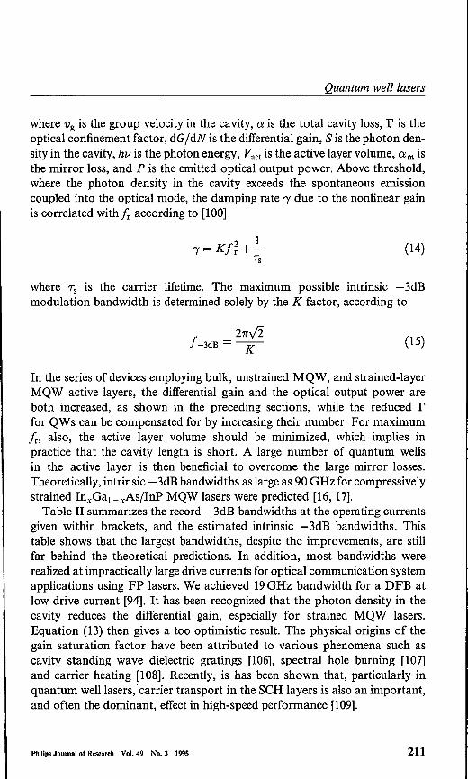
5. Reliability of strained-layer InGaAs(P) MQW lasers
5.1. 1480 nm high power lasers
High-power lasers emitting at 1480nm are key components for pumpingEr3+-doped fibres which are used as all-opticalamplifiers (EDFA) in opticalcommunication systems. We fabricated four-well 0.8% compressively strainedInGaAs DCPBH-MQW lasers emitting at 1480nm. Devices with 1mm cavitylength and facets coated to Rf = 5% and R; = 95% show threshold currentsof 30mA at room temperature. At 325mA drive current, typically 100mWoutput power is obtained, which .increases to 160mW at 500mA drivecurrent. Averaged emission wavelengths at 80mW CW output power of1482.2 ± 7.9 nm (231 lasers), 1482.3 ± 5.4 (111 lasers) and 1482.0 ± 4.5 nm(75lasers) were measured for the numbers of lasers given within the brackets,mounted from three different wafers. For evaluation of reliability, 24lasers (12samples from two different wafers), which did not undergo either a burn-in
212 Philip. Journal of Research Vol.49 No.3 1995
Quantum wel/lasers
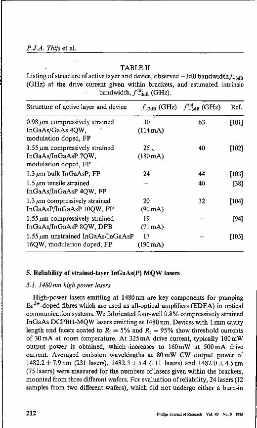
or any other screening, were lifetested for 9500 hours at 70°C heatsinktemperature at 500mA constant drive current. In this lifetest, the estimatedjunction temperature was approximately 100°C, and under these conditionsmost of the lasers emitted CW output powers up to 80 to 90mW. Figure16 shows the cumulative lognormal distribution of lifetimes, defined in thiscase as the time required for a 50% reduction in output power from the initialvalue. (One laser was excluded from the ànalysis because, after 4500 hours, itsmonitored output power was significantly higher than its initial value, whereasthe threshold current remained the same. It was verified that this was causedby a defective detector.) For the extrapolation, the output decreasing ratewas assumed to be constant at the value observed in the 9500 hours testtime. The projected median lifetime at 70°C is estimated to be as large as3.25 x 105h (37 years) with a dispersion of only 0.43 x 10⁵h. The saturationof the decrease in output power, which is generally observed, results in longerlifetimes in practice.
In this section, the high reliability of 1480nm strained-layer InGaAsjInPMQW pump lasers was demonstrated. In total, 233000 hours of testing at70°C heatsink temperature (lOO°C junction temperature) and 80 to 90mWoutput power without any device failure were recorded, demonstrating theapplicability of strained-layer InGaAs MQW lasers as reliable pump sourcesfor EDFAs.
Philips Joumal of Research Vol.49 No.3 1995 213
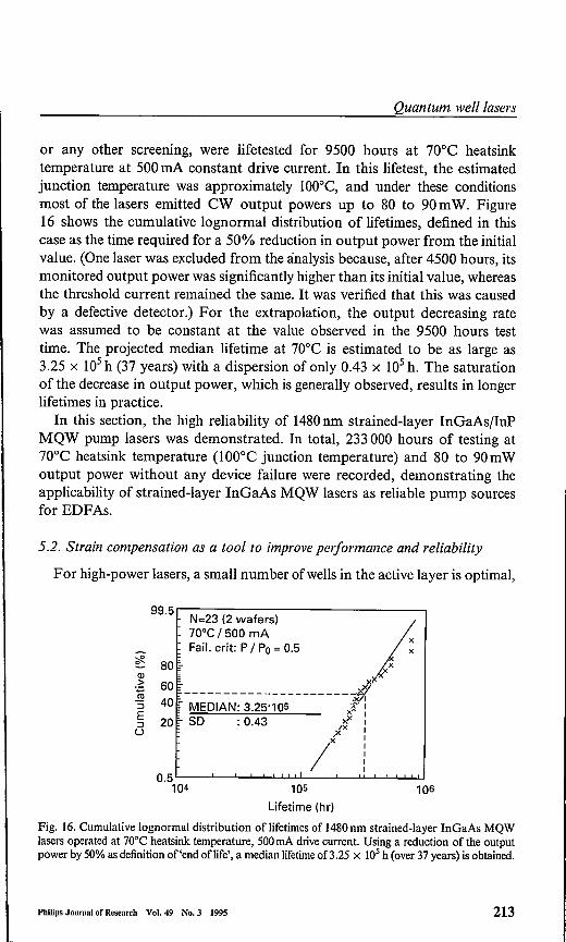
5.2. Strain compensation as a tool to improveperformance and reliability
For high-power lasers, a small number ofwells in the active layer is optimal,
99.5
~ 80Ol> 60..;:::;~ 40::JE 20::JU
N=23 (2 wafers) I70°C/ 500 mA
X
xx
Fail. crit: P / Po = 0.5
xl'
---------------------~MEDIAN: 3.25·105 x:£· :SD ·043 XX I• • IX I
,X I
IX i105
Lifetime (hr)
Fig. 16. Cumulative lognormal distribution oflifetimes of 1480nm strained-layer InGaAs MQWlasers operated at 70°C heatsink temperature, 500mA drive current. Using a reduction ofthe outputpower by 50% as definition of 'end oflife', a median lifetimeof3.25 x 105h (over 37years) is obtained.
0.5 '--_.,L_-'--'-....L....l....L.L..u__---'-_U-J---'-..J...J..~
104 106
P.J.A. Thijs et al.
and, as demonstrated above, the reliability is not negatively affected. Forcertain applications, e.g. wavelength-tunable distributed Bragg reflector(DBR) lasers or high-speed lasers, devices operating at larger threshold gainare desired. In order to maintain the advantages of QWs, bandfilling effectsmust be prevented by increasing the number of wells. The net strain in sucha structure may then become so large that the reliability is negatively affected.A possibility of reducing or even eliminating any net strain in the structure isthe application of strain compensation by growing opposite strains in the wellsand barrier and/or separate confinement heterostructure (SCH) layers [110],asindicated by
(16)
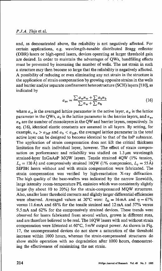
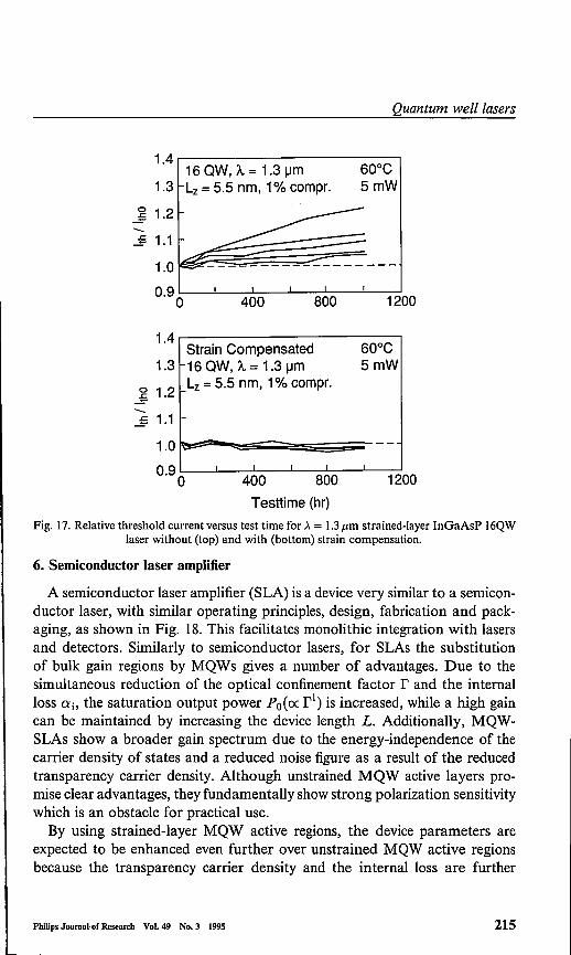
where aav is the averaged lattice parameter in the active layer, aw is the latticeparameter in the QWs, ab is the lattice parameter in the barrier layers, and nw,nb are the number ofmonolayers in the QW and barrier layers, respectively. Ineq. (16), identical elastic constants are assumed in all layers. By setting, forexample, aw > aInP and ab < aInP, the averaged lattice parameter in the totalactive layer can be designed to become identical to that of the InP substrate.The application of strain compensation does not lift the critical thicknesslimitation for each individual layer, however. The effect of strain compen-sation on performance and reliability was studied on 1.3pm wavelengthstrained-layer InGaAsP MQW layers. Tensile strained 4QW (1% tension,i; = 120Á) and compressively strained 16QW (1% compression, i; = 55Á)SIPBH lasers without and with strain compensation were fabricated. Thestrain compensation was verified by high-resolution X-ray diffraction.The high quality of the base-wafers was indicated by the narrow linewidth,large intensity room-temperature PL emission which was consistently slightlylarger (by about 10 to 20%) for the strain-compensated MQW structures.Also, smaller laser threshold currents and slightly larger differential efficiencieswere observed. Averaged values at 20°C were: llh = 16mA and 7J = 67%versus 11.6mA and 68% for the tensile strained and 12mA and 57% versus9.5mA and 62% for the compressively strained devices. These trends wereobserved for lasers fabricated from several wafers, grown in different runs,and are therefore believed to be real. The 16QWlasers with and without straincompensation were lifetested at 60°C, 5mW output power. As shown in Fig.17, the uncompensated devices do not show a saturation of the thresholdincrease within 1000 hours, whereas the strain-compensated structures doshow stable operation with no degradation after 1000 hours, demonstrat-ing the effectiveness of minimizing the net strain.
214 Philip. Journal of Research Vol.49 No.3 1995
Quantum wel/lasers
1.4 .-------------,60°C5mW
16 OW, À. = 1.3 IJm1.3 Lz = 5.5 nm, 1% compr.
_§ 1.2
--..É 1.1 ~~~~~.
1.0
0.9 0l:------l.--:-4~00=--_J_--::8-:-00::--,------;1-=200
1.4Strain Compensated 60°C
1.3 16 OW, À. = 1.3 IJm 5mW
0 1.2Lz = 5.5 nm, 1% compr.
..É-- 1.1..É
1.0 -"""0.9
0 400 800 1200
Testtime (hr)Fig. 17. Relative threshold current versus test time for À = 1.3pm strained-layer InGaAsP 16QW
laser without (top) and with (bottom) strain compensation.
Philips Journal of Research Vol.49 No.3 1995 215
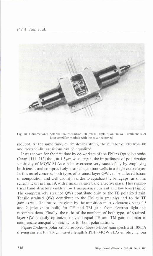
6. Semiconductor laser amplifier
A semiconductor laser amplifier (SLA) is a device very similar to a semicon-ductor laser, with similar operating principles, design, fabrication and pack-aging, as shown in Fig. 18. This facilitates monolithic integration with lasersand detectors. Similarly to semiconductor lasers, for SLAs the substitutionof bulk gain regions by MQWs gives a number of advantages. Due to thesimultaneous reduction of the optical confinement factor r and the internalloss ai> the saturation output power Po(r:x. rl) is increased, while a high gaincan be maintained by increasing the device length L. Additionally, MQW-SLAs show a broader gain spectrum due to the energy-independence of thecarrier density of states and a reduced noise figure as a result of the reducedtransparency carrier density. Although unstrained MQW active layers pro-mise clear advantages, they fundamentally show strong polarization sensitivitywhich is an obstacle for practical use.
By using strained-layer MQW active regions, the device parameters areexpected to be enhanced even further over unstrained MQW active regionsbecause the transparency carrier density and the internal loss are further
P.J.A. Thijs et al.
Fig. 18. Unidirectional polarization-insensitive l300nm multiple quantum well semiconductorlaser amplifier module with the cover removed.
reduced. At the same time, by employing strain, the number of electron-hhand electron-lh transitions can be equalized.
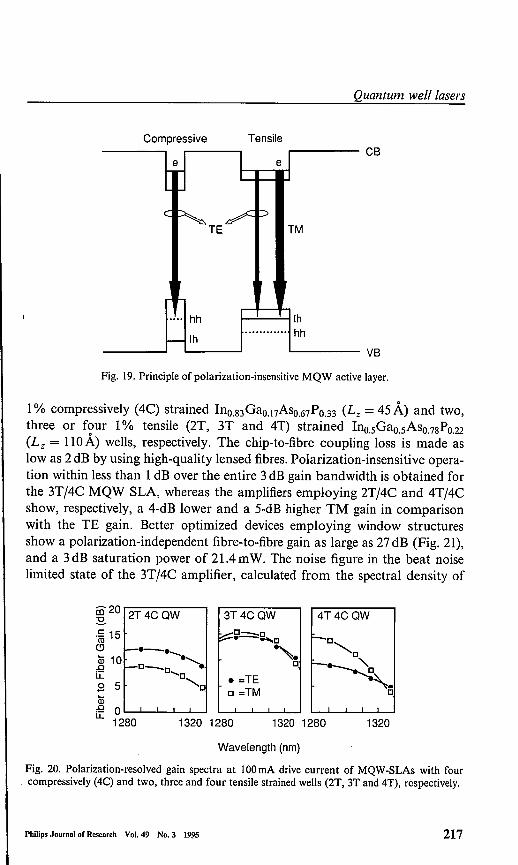
It was shown for the first time by co-workers of the Philips OptoelectronicsCentre [111-113] that, at 1.3 j.Lm wavelength, the impediment of polarizationsensitivity of MQW-SLAs can be overcome very successfully by employingboth tensile and compressively strained quantum wells in a single active layer.In this novel concept, both types of strained-layer QW can be tailored (strainor composition and well width) in order to equalize the bandgaps, as shownschematically in Fig. 19, with a small valence band effective mass. This symme-trical band structure yields a low transparency current and low loss (Fig. 5).The compressively strained QWs contribute only to the TE polarized gain.Tensile strained QWs contribute to the TM gain (mainly) and to the TEgain as well. The ratios are given by the transition matrix elements being 0.5and 2 (relative to bulk) for TE and TM gain from electron-light-holerecombinations. Finally, the ratio of the numbers of both types of strained-layer QW is easily optimized to yield equal TE and TM gain in order tocompensate unequal confinements for both polarizations.
Figure 20 shows polarization resolved (fibre-to-fibre) gain spectra at 100mAdriving current for 750 ust: cavity length SIPBH-MQW SLAs employing four
216 Philips Journalof Research Vol.49 NO.3 1995
Quantum wel/lasers
Compressive Tensile
e e
c~TE/
pTM
~~.. hh Ih............ hh
I-- Ih
CB
Fig. 19. Principle of polarization-insensitive MQW active layer.
VB
1% compressively (4C) strained Ino.83Gao.17Aso.67Po.33(L; = 45Á) and two,three or four 1% tensile (2T, 3T and 4T) strained Ino.sGao.sAso.78Po.22(L, = 110Á) wells, respectively. The chip-to-fibre coupling loss is made aslow as 2 dB by using high-quality lensed fibres. Polarization-insensitive opera-tion within less than 1dB over the entire 3dB gain bandwidth is obtained forthe 3T/4C MQW SLA, whereas the amplifiers employing 2T/4C and 4T/4Cshow, respectively, a 4-dB lower and a 5-dB higher TM gain in comparisonwith the TE gain. Better optimized devices employing window structuresshow a polarization-independent fibre-to-fibre gain as large as 27dB (Fig. 21),and a 3dB saturation power of 21.4 mW. The noise figure in the beat noiselimited state of the 3T/4C amplifier, calculated from the spectral density of
ED20 2T 4C OW~.~ 15<9 1---._.........~ 1°I--D_ <,._ D .....L1.. D,.s 5 'cIDff: 0 .___.__..._........_......__.
1280 1320 1280
3T4COWk......P-c~.-.,[]
<,c
• =TED =TM
1320 1280 1320
Wavelength (nm)
Fig. 20. Polarization-resolved gain spectra at 100mA drive current of MQW-SLAs with fourcompressively (4C) and two, three and four tensile strained wells (2T, 3T and 4T), respectively.
Philip. Journalof Research Vol. 49 No.3 1995 217
P.J.A. Thijs et al.
30
27
24
III 21
"c:: 18ëiiCl
~ 15:J
" 120~
9
6
3
01280
5°C,500mA
1290 1300 1310 1320 1330
Wavelength, nm
Fig. 21. TE and TM fibre-to-fibre gain at 500mA drive current and a chip temperature of 5°C ofthe unidirectional amplifier module. The extremely low ripple indicates the low reflectivities of all
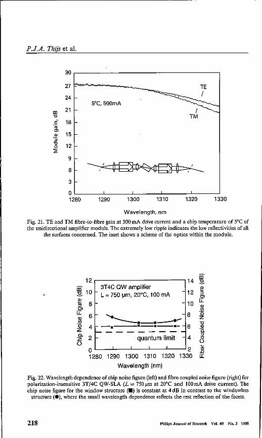
the surfaces concerned. The inset shows a scheme of the optics within the module.
12 141iI:E!..
çg 103T4C OW amplifier Ol
12 ...L = 750 IJm, 20°C, 100 mA ::J
Cl~ 8 10 iJ:::J OlCl (/l
ü: 6 ..... 8 'sID zCl) '-----.---.----.- "'s 4 -. .---.--.- 6 Olz ----- 0..0. quantum limit 4
::J
:ë 2 0
Ü Ü...0 2 Ol
.c1280 1290 1300 1310 1320 1330 iJ:
Wavelength (nm)
Fig. 22. Wavelength dependence of chip noise figure (left) and fibre coupled noise figure (right) forpolarization-insensitive 3T/4C QW-SLA (L = 750 Jlm at 20°C and 100mA drive current). Thechip noise figure for the window structure (.) is constant at 4dB in contrast to the windowlessstructure (e),where the small wavelength dependence reflects the rest reflection of the facets.
218 Phllips JournnI er Research Vol. 49 No. 3 1995
Quantum wel/lasers
the amplified spontaneous emission, is shown as a function of wavelength inFig. 22. This illustrates the importance ofminimizing the facet reflectivity. Indevices with a window structure, a low fibre coupled noise figure of 6 dB (chipnoise figure only 4 dB) is observed over the wavelength range 1290to 1325 nm.The latter has been confirmed by recent experiments using the strained-layerMQW SLA as an optical preamplifier [114]. The small chip noise figure of4 dB resulted in a preamplified receiver sensitivity of -30.3 dB at 10 Gbit/sfor a bit error rate (BER) of 10-9• This represents a significant improvementover the value of -13.7 dBm achieved without optical preamplification.The above principle of employing both tensile and compressively strained
QWs in one single active layer so as to balance the TE and TM gain is alsoapplicable at 1.5J.Lm wavelength.
7. Conclusions
The enhanced performance of strained-layer InP-based semiconductorlasers is a result of the reshaping of the valence band structure due to thetetragonal deformation of the crystal lattice, which leads to a reduction ofthe in-plane hole effective mass, Auger recombination, and intervaleneeband absorption. The improvements reported to date include reduced thresh-old current densities to values as low as approximately 100A/cm2, facilitatingthe fabrication of sub-mA threshold current lasers, enhanced differentialefficiencies, leading to record high CW output powers, and reduced linewidthenhancement factors less than 1.Furthermore, the polarization ofthe emissioncan be controlled.
Improvements, smaller than those predicted theoretically, for the temperaturedependence of the threshold current (To) and for the high-speed characteristicswere observed. This is attributed to incomplete removal of Auger processes,and larger gain saturation and carrier transport limitations, respectively.Nevertheless, the record values were set by strained devices.
Strained-layer MQW devices show high reliability. A median lifetime of3.25 x 105h (37 years) with a small standard deviation of 0.43 x 10⁵ h wasdeduced from studies running over 233 000 h of device testing without observingany failure. Furthermore, strain compensation is shown to be a useful tool forimproving the performance and reliability of devices with high total strain.The combination ofboth compressively and tensile strained QWs in a single
active region can be used to lift the fundamental polarization sensitivity ofMQW SLAs. Using this approach, compact SLA modules showing 27 dBpolarization-independent chip gain with saturation output powers of21.4mWand noise figures as low as 4 dB were demonstrated. This implies
Philips Journalof Research Vol. 49 No. 3 1995 219
P.J.A. Thijs et al.
that strained-layer MQW SLAs are not only important candidates as booster-amplifiers, but also as repeater- and pre-amplifiers in existing optical fibrecommunication systems.
Acknowledgments
The authors wish to thank A. van Leerdam, G.L.A. van der Hofstad,I.M.M. van der Heij<!en, E.I. lansen, I. Donkers, I.C.N. Rijpers, L.I.M.Hendrix, M.H.C. Vermeulen-Hartjes, R.W.M. Slootweg, C.I. van der Poel,P.1. Kuindersma, A.I.M. Verboven, H. van Tongeren, I.W. Kokkeling,R. van Roemburg and F. van Dorst for their contributions to this work.Professor A.R. Adams, E. O'Reilly, and members of their group at SurreyUniversity are thanked for valuable discussions and for making hydrostaticpressure measurements on strained-layer MQW lasers.
REFERENCES[1] W.D. Laidig, P.J. CaldweIl, Y.F. Lin and C.K. Peng, Appl. Phys. Lett., 44,653 (1984).[2] A.R. Adams, Electron. Lett., 22, 249 (1986).[3] E. Yablonovitch and E.O. Kane, J. Lightwave Technol., LT-4,504 (1986); see also J. Light-
wave Technol., LT-4, 961 (1986).[4] E. Yablonovitch and E.O. Kane, J. Lightwave Technol., 6, 1292(1988).[5] P.J.A. Thijs and T. van Dongen, Electron. Lett., 25, 1735 (1989).[6] P.T. Landsberg, Solid State Electron., 30, 1107(1987).[7] A. Sugimura, IEEE J. Quantum Electron., QE-17, 627 (1981).[8] N.K. Dutta and R.J. Nelson, J. Appl. Phys., 53, 74 (1982).[9] M. Asada, A.R. Adams, K.E. Stubkjaer, Y. Suematsue, Y. Itaya and S. Arai, IEEE J.
Quantum Electron., QE-17, 611 (1981).[10] M. Asada, A. Kameyama and Y. Suematsue, IEEE J. Quantum Electron., QE-20, 745
(1984).[11] A.R. Adams, K.C. Heasman and J. Hilton, Semicond. Sci. Technol., 2, 761 (1987).[12] J.W. Matthews and A.E. Blakeslee, J. Crystal Growth, 27, 118 (1974).[13] M.P.C.M. Krijn, G.W. 't Hooft, M.J.B. Boermans, P.J.A. Thijs, T. van Dongen, J.J.M.
Binsma and L.F. Tiemeijer, Appl. Phys. Lett., 61, 1772 (1992).[14] K.J. Vahala and C.E. Zah, Appl. Phys. Lett., 52, 1945 (1988).[15] T. Ohtoshi and N. Chinone, IEEE Photon. Technol. Lett., 1, 117(1989).[16] A. Ghiti, E.P. O'Reilly and A.R. Adams, Electron. Lett., 25, 821 (1989).[17] 1 Suemune, L.A. Coldren, M. Yamanishi and Y. Kan, Appl. Phys. Lett., 53,1378 (1988).[18] R.E. Cavicchi, D.V. Lang, D. Gershoni, A.M. Sergent, J.M. Vandenberg, S.N.G. Chu and
M.B. Panish, Appl. Phys. Lett., 54, 739 (1989).[19] M.P. Houng and Y.C. Chang, J. Appl. Phys., 65,3092 (1989).[20] S. Corzine and L.A. Coldren, Appl. Phys. Lett., 59, 588 (1991).[21] M. Nido, K. Naniwae, J. Shimizu, S. Murata and A. Suzuki, IEEE J. Quantum Electron.,
QE-29, 885 (1993).[22] S. Fourohar, A. Ksendov, A. Larsson and H. Temkin, Electron. Lett., 28, 1431 (1992).[23] J.S. Major, Jr., D.W. Nam, J.S. Osinski and D.F. Welch, IEEE Photon. Technol. Lett., 5,
594 (1993).[24] S. Adachi, J. Appl. Phys., 53,8775 (1982).[25] P.J.A. Thijs, J.J.M. Binsma, L.F. Tiemeijer and T. van Dongen, Tech. Dig. ECOC/IOOC,
Paris, France, 2, 31 (1991).[26] G. Jones, M. Silver, M. Hawley, E.P. O'Reilly, A.R. Adams and P.J.A. Thijs, Tech. Dig.
13th IEEE Int. Semiconductor Laser Conf., Takamatsu, Japan, 30, Paper CS (1992).
220 Philips Journalof Research Vol.49 No.3 1995
Quantum weil lasers
(27) P.J.A. Thijs, T. van Dongen, L.F. Tiemeijer and J.J.M. Binsma, J. Lightwave Techno!.,LT-12, 28 (1994).
(28) P.J.A. Thijs, T. van Dongen, L.F. Tiemijer, R.W.M. Slootweg and J.J.M. Binsma, Tech.Dig. ECOC/IOOC, Paris, France, 3, 48 (1991).
(29) D. Coblentz, T. Tanbun-Ek, R.A. Logan, A.M. Sergent, S.N.G. Chu and P.S. Davisson,App!. Phys. Lett., 59, 405 (1991).
(30) C.E. Zah, R. Bhat, F.J. Favire, M. Koza, T.P. Lee, D. Darby, D.C. Flanders and J.J. Hsieh,Electron. Lett., 28, 2323 (1992).
(31) M. Yamamoto, N. YamamotoandJ. Nakano, Proc. 5th Int. Conf. InP and Related Mater.,Paris, France, 231, paper TuB2 (1993).
(32) A. Kasukawa, Y. Imajo, T. Namegaya, Y. Hiratani and T. Kikuta, Proc. 13th IEEE Int.Semiconductor Laser Conf., Takamatsu, Japan, 200, paper K4 (1992).
(33) H.Q. Hou and C.W. Tu, J. Crystal Growth, 120, 167 (1992).(34) E.W.A. Young, G.M. Fontijn, C.J. Vriezema and P.C. Zalm, J. App!. Phys., 70, 3593
(1991).(35) E.W.A. Young and G.M. Fontijn, J. Crystal Growth, 107, 274 (1991).(36) A.T. Macrander, J.A. Long, U.G. Rigg, A.F. Bloemeke and W.D. Johnson, Jr., App!. Phys.
Lett., 45, 1297 (1984).(37) P.J.A. Thijs, J.J.M. Binsma, L.F. Tiemeijer and T. van Dongen, Electron. Lett., 28, 829
(1992).(38) P.J.A. Thijs, L.F. Tiemeijer, P.1. Kuindersma, J.J.M. Binsma and T. van Dongen, IEEE J.
Quantum Electron., QE-27, 1426 (1991).(39) P.J.A. Thijs, J.J.M. Binsma, L.F. Tiemeijer, P.1. Kuindersma and T. van Dongen, J. Micro-
electron. Eng., 18, 57 (1992).(40) J.S. Osinski, Y. Zou, P. Grodzinski, A. Mathur and P.D. Dapkus, IEEE Photon. Techno!.
Lett.,4, 10 (1992).(41) L.F. Tiemeijer, P.J.A. Thijs, J.J.M. Binsma and T. van Dongen, App!. Phys. Lett., 60,554
(1992).(42) J.S. Osinski, P. Grodzinsky, Y. Zou and P.D. Dapkus, Electron. Lett., 27, 469 (1991).(43) J.E.A. Whiteaway, G.H.B. Thompson, P.D. Greene and R.W. Glew, Electron. Lett., 26,
340 (1990).(44) P.W.A. McIlroy, A. Kurobe and Y. Uematsu, IEEE J. Quantum Electron., QE-21, 1958
(1985).(45) J.Z. Wilcox, G.L. Peterson, S. Ou, JJ. Yang, M. Jansen and D. Schechter, J. App!. Phys.,
64,6564 (1988).(46) A. Ougazzaden, A. Mircea, R. MelJet, G. Primot and C. Kazmiersky, Electron. Lett., 28,
1078 (1992).(47) P. Grodzinski, J.S. Osinski, Y. Zou, A. Mathur and P.D. Dapkus, Tech. Dig. 4th Conf. on
InP and Related Mater., Newport, USA, 449 (1992).(48) J.S. Osinski, P. Grodzinski, Y. Zou, P.D. Dapkus, Z. Karim and A.R. Tanguary, Jr., IEEE
Photon. Techno!. Lett., 4, 1313 (1992).(49) C.E. Zah, R. Bhat, B. Pathak, C. Caneau, F.J. Favire, N.C. Andreadakis, D.M. Hwang,
M.A. Koza, C.Y. Chen and T.P. Lee, Electron. Lett., 27,1414 (1991).[50) W.T. Tsang, F.S. Choa, M.C. Wu, Y.K. Chen, A.M. Sergent and P.F. Sciortino, Jr., App!.
Phys. Lett., 58, 2610 (1991).[51) C. Starck, J.Y. Emery, R.J. Simes, M. Matabon, L. Goldstein and J. Barreau, J. Crystal
Growth, 120, 180 (1992).[52) C.E. Zah, R. Bhat, F.J. Favire, S.G. Menocal, N.C. Andreadakis, K.W. Cheung, D.M.
Hwang, M.A. Koza and T.P. Lee, IEEE J. Quantum Electron., QE-27, 1440 (1991).[53) A.T.R. Briggs, P.D. Greene and J.M. Jowett, IEEE Photon. Techno!. Lett., 4, 423
(1992).[54) R. Bhat, C.E. Zah, M.A. Koza, D.M.D. Hwang, F.J. Favire and B. Pathak, Tech. Dig. 4th
Conf. on InP and Related Mater., Newport, USA, 453 (1992).[55) H. Hirayama, Y. Miyake and M. Asada, IEEE J. Quantum Electron., QE-28, 68 (1992).[56) E.P. O'Reilly, G. Jones, A. Ghiti and A.R. Adams, Electron. Lett., 27,1417 (1991).[57) D. Teng, Y.H. Lo, H. Lin and L.F. Eastman, App!. Phys. Lett., 60, 2729 (1992).[58) G.A. Acket, P.J.A. Thijs, J.J.M. Binsma, L.F. Tiemeijer, A. Valster, C.J. van der Poel and
M.J.B. Boermans, in H.W.M. Salemink and M.D. Pashley (eds.), Semiconductor Interfaces
Philip. Journalof Research Vol.49 No.3 1995 221
P.J.A. Thijs et al.
[59]
[60][61]
to the Sub-Nanometer Scale, Kluwer Academic Publishers, The Netherlands, pp. 241-249,(1993).A. Valster, C.J. van der Poel, M.N. Finke and M.J.B. Boermans, Proc. 13th IEEE Int.Semiconductor Laser Conf., Takamatsu, Japan, 152, paper GI (1992).P.J.A. Thijs, Proc. 13th IEEE Int. Semiconductor Laser Conf., Takamatsu, Japan, 2 (1992).A.R. Adams, K.C. Heasman and E.P. O'ReiIly, in R.A. Abram and M. Jaros (eds.), BandStructure Engineering in Semiconductor Microstructures, Plenum Publishing Corp., 279(1989).A.P. Mozer, S. Hauser and M.H. Pilkuhn, IEEE J. Quantum Electron., QE-21, 719 (1985).J.D. Lambkin, B.J. Gunney, D. Lancefield, F.G. Bristow and D.J. Dunsten, J. Phys. E: Sci.Instru., 21, 763 (1988).W.S. Ring, A.R. Adams, P.J.A. Thijs and T. van Dongen, Electron. Lett., 28, 569 (1992).A.R. Adams, M. Hawley, E.P. O'Rcilly and W. Ring, Jap. J. App!. Phys., supp!. 32-1, 358(1993).G. Fuchs, J. Hörer, A. Hangleiter, V. Härle, F. Scholz, R.W. Glew and L. Goldstein, Appl,Phys. Lett., 60, 231 (1992).K.C. Heasman, E.P. O'ReiIly, G.P. Witchlow, W. Batty and A.R. Adams, SPIE, 800, 50(1987).E.P. O'Reilly and M. Silver, App!. Phys. Lett., 63, 3318 (1993).W. Nijman, P. Post and G.A. Acket, Gallium Arsenide and Related Compounds, Instituteof Physics, Bristol, 56,579 (1981).P. Blood, SPIE, 861, 34 (1987).P.J.A. Thijs, L.F. Tiemeijer, T. van Dongen and J.J.M. Binsma, Tech. Dig. Opt. FiberCommun. Conf., San Jose, CA, 80, paper WBI (1992).M. Hawley, Univ. of Surrey, private communication.Y. Zou, J.S. Osinski, P. Grodzinski, D.P. Dapkus, W. Rideout, W.F. Sharfin and F.D.Crawford, IEEE Photon. Techno!. Lett., 4, 1315 (1992).A.R. Adams, V.A. Wilkinson, J. Braithwaite, M. Silver and E.P. O'ReiIly, Proc. 13th IEEEInt. Semiconductor Laser Conf., Takamatsu, Japan, 26, paper C3 (1992).J. Barrau, B. Brousseau, M. Brousseau, R.J. Simes and L. Goldstein, Electron. Lett., 28,786 (1992).P.J.A. Thijs, J.J.M. Binsma, E.W.A. Young and W.M.E. van Gils, Electron. Lett., 27, 791(1991).L.E. Eng, A. Sa'ar, T.R. Chen, I.Grave, N. Kuze and A. Yariv, App!. Phys. Lett., 58, 2752(1991).H. Temkin, N.K. Dutta, T. Tanbun-Ek, R.A. Logan and A.M. Sergent, App!. Phys. Lett.,57, 1610 (1990).P.J.A. Thijs, J.J.M. Binsma, L.F. Tiemeijer, R.W.M. Slootweg, R. van Roijen and T. vanDongen, App!. Phys. Lett., 60, 3217 (1992).C.E. Zah, F.J. Favire, R. Bhat, S.G. Menocal, N.C. Andreadakis, D.M. Hwang, M. Kozaand T.P. Lee, IEEE Photon. Techno!. Lett., 2, 852 (1990).C.H. Henry, IEEE J. Quantum Electron., QE-18, 259 (1982).T.L. Koch and R.A. Linke, Appl, Phys. Lett., 48, 613 (1986).L.F. Tiemeijer, P.J.A. Thijs, J.J.M. Binsma and T. van Dongen, Appl, Phys. Lett., 60, 2466(1992).S. Murata, A. Tomita and A. Suzuki, IEEE Photon. Techno!. Lett., 5, 16 (1993).N.K. Dutta, H. Temkin, T. Tanbun-Ek and R.A. Logan, App!. Phys. Lett., 57, 1390(1990).K. Kikuchi, M. Kakui, C.E. Zah and T.P. Lee, IEEE Photon. Techno!. Lett., 3, 314(1991).M. Okai, M. Suzuki and T. Taniwatari, Proc. CLEO, Baltimore, USA, paper CPD4-1/8(1993).K. Kano, Y. Yoshikuni, M. Fukuda and J. Yoshida, IEEE Photon. Techno!. Lett., 3,877(1991).M. Okai, T. Tsuchiya, K. Uomi, N. Chinone and T. Harada, IEEE Photon. Techno!. Lett.,2, 529 (1990).M. Okai, T. Tsuchiya and A. Takai, IEEE Photon. Techno!. Lett., 4, 526 (1992).H. Bissessur, C. Starck, J.Y. Emery, F. Pommereau, C. Duchemin, J.G. Provost, J.L. Beylatand B. Fernier, Electron. Lett., 28, 998 (1992).
[62][63]
[64][65]
[66]
[67]
[68][69]
[70][71]
[72][73]
[74]
[75]
[76]
[77]
[78]
[79]
[80]
[81][82][83]
[84][85][86]
[87]
[88]
[89]
[90][91]
222 Philip. Journalof Research Vol.49 No.3 1995
Philip. Journalof Research Vol. 49 No. 3 1995 223
Quantum weil lasers
[92] Y. Matsui, T. Kunii, H. Horikawa and T. Kamijoh, IEEE Photon. Techno!. Lett., 3, 424(1991).
[93] Y. Matsui, T. Kunii, H. Horikawa and T. Kamijoh, Tech. Dig. Opt. Fiber Commun. Conf.,San Diego, CA, 202 (1991).
[94] P.1. Kuindersma, W. Scheepers, J.J.M. Binsma, P.J.A. Thijs and T. van Dongen, PhilipsOptoelectronics Centre, private communication.
[95] P.1. Kuindersma, W. Scheepers, J.H.M. Cnoops, P.J.A. Thijs, G.L.A. van der Hofstad,T. van Dongen and J.J.M. Binsma, Tech. Dig. 12th IEEE Int. Semiconductor LaserConf., Davos, Switzerland, 248, Paper M4 (1990).
[96] Y. Hirayama, N. Suzuki, M. Onomura, M. Morinaga, M. Funemizu, M. Kushibe andM. Nakamura, Tech. Dig. Opt. Fiber Commun. Conf., San Diego, CA, 69, paper WB4(1991).
[97] Y. Matsui, M. Nakajima, H. Horikawa, T. Kunii, Y. Ogawa and T. Kamijoh, Tech. Dig.Opt. Fiber Commun. Conf., San Jose, CA, 271, paper FB2 (1992).
[98] H. Temkin, S. Mahajan, M.A. DiGiuseppe and A.G. Dentai, App!. Phys. Lett., 40, 562(1982).
[99] P.J.A. Thijs, E.A. Montie, T. van Dongen and C.W.T. Bulle-Lieuwma, J. Crystal Growth,105, 339 (1990).
[100] R. Olshansky, P. Hill, V. Lanzisera and W. Powazinik, IEEE. J. Quantum Electron, QE-23,1410 (1987).
[101] J.D. Ralston, S.Weisser,E.C. Larkins, I.Esquivias, P.J. Tasker, J. Fleissner and J. Rosenzweig,Tech. Dig. 13th IEEE Int. Semiconductor Laser Conf., Takamatsu, Japan, 9, paper PD5(1992).
[102] P.A. Morton, R.A. Logan, T. Tanbun-Ek, P.F. Sciortino, Jr., A.M. Sergent, R.K. Mont-gomery and B.T. Lee, Electron. Lett., 28,2156 (1992).
[103] E. Meland, R. Holmstrom, J. Schlafer, R.B. Lauer and W. Powazinik, Electron. Lett., 26,1827 (J 990).
[104] H. Lipsanen, D.L. Coblenz, R.A. Logan, R.D. Yadvish, P.A. Morton and H. Temkin,IEEE Photon. Techno!. Lett., 4, 673 (1992).
[105] I.F. Lealman, M. Bagley, D.M. Cooper, N. Fletcher, M. Harlow, S.D. Perrin, R.H. Wallingand L.D. Westbrook, Electron. Lett., 27, 1191 (1991).
[106] J. Eom and C.B. Su, App!. Phys. Lett., 54,1734 (1989).[107] K. Uomi, T. Tsuchiya, M. Aoki and N. Chinone, App!. Phys. Lett., 58, 675 (1991).[108] B. Gomatan and A.P. Defonzo, IEEE J. Quantum Electron., QE-26, 1689 (1990).[109] R. Nagarajan, M. Ishikawa, T. Fukushima, R.S. Geels and J.E. Bowers, IEEE J. Quantum
Electron., QE-28, 1990 (1992).[IlO] B.1. Miller, U. Koren, M.G. Young and D.M. Chien, App!. Phys. Lett., 58,1952 (1991).[Ill] L.F. Tiemeijer, P.J.A. Thijs, T.van Dongen, R.W.M. Slootweg, J.M.M. van der Heijden,
J.J.M. Binsma and M.P.C.M. Krijn, Proc. 18th ECOC, Berlin, Germany, part 3, 911, paperPDII.6 (J 992).
[112] L.F. Tiemeijer, P.J.A. Thijs, T.van Dongen, R.W.M. Slootweg, J.M.M. van der Heijden,J.J.M. Binsma and M.P.C.M. Krijn, App!. Phys. Lett., 62, 826 (1993).
[113] L.F. Tiemeijer, P.J.A. Thijs and J.J.M. Binsma, Tech. Dig. Opt. Amplifiers and App!.,Breckenridge, CO, USA, 34 (1994).
[114] H. de Waardt, L.F. Tiemeijer and B.H. Verbeek, IEEE Photon. Techno!. Lett., 6, 645(1994).
P.J.A. Thijs et al.
Authors
224
Peter J.A. Thijs received his degree in chemistry from the EindhovenPolytechnic Institute, Eindhoven, The Netherlands, in 1974, the BScand MSc degrees (cum laude) in chemical engineering from the EindhovenUniversity of Technology in 1981 and 1983, respectively, and the PhDdegree (cum laude) in electronics engineering from the Delft Universityof Technology, Delft, The Netherlands, in 1994.
In 1975 he joined Philips Research Laboratories, Eindhoven, where hewas involved in the liquid phase epitaxial growth of AIGaAs-GaAs forsemiconductor lasers and the associated characterization techniques.From 1982 to 1985 he worked on the liquid phase epitaxial growth ofInGaAsP-InP and the associated characterization techniques. Sincethen, he has studied the low-pressure organometallic vapour phaseepitaxial growth of InGaAsP-InP and AIGaInAs-InP for activeoptoelectronic devices such as Fabry-Perot, distributed feedback anddistributed Bragg reflector lasers, amplifiers, detectors, and passiveelements such as waveguides, couples and switches. His current researchinterests are in strained and unstrained quantum well optoelectronicdevices. He has authored and coauthored over 80 papers in internationaljournals and conference proceedings, is frequently awarded invitedpapers, and has served as a programme committee member in severalinternational conferences.
Luuk F. Tiemeijer received the Doctorandus degree in experimentalphysics from the State University of Utrecht, The Netherlands, in 1986,and the PhD degree in electronics from the Delft University of Tech-nology in 1992.
In 1986 he joined Philips Research Laboratories, Eindhoven, where heis currently conducting research on InGaAsP semiconductor lasers andamplifiers.
J.J.M. Binsma received the BSc and MSc degrees in chemistry (both cumlaude) from the State University of Utrecht in 1976 and 1977, respec-tively, and the PhD degree in solid state chemistry from the CatholicUniversity of Nijmegen, The Netherlands, in 1981.
From 1981 to 1985 he worked at the Interuniversity Reactor Institute,Delft, on surface chemistry and crystal growth. In 1985 he joined PhilipsResearch Laboratories, Eindhoven, where he is engaged in work on long-wavelength lasers and optoelectronic integrated circuits.
Teus van Dongen received his degree in physical engineering from theEindhoven Polytechnic Institute in 1975.
In 1968 he joined Philips Research Laboratories, Eindhoven. He wasinvolved in the technology of III-V compounds for Gunn diodes,LEDs and GaAs-AIGaAs lasers until 1980. Since then, he has beeninterested in the liquid phase epitaxial growth of InGaAsP-InP andthe associated characterization techniques. In 199 I he became involvedin the low-pressure organometallic vapour phase epitaxial growth ofInGaAsP-InP for long wavelength optoelectronic devices.
Philips Journalof Research Vol.49 No.3 1995