ddr2 memory interface termination, drive strength, loading, and … · 2020-01-29 · this...
TRANSCRIPT
© July 2008 Altera Corporation AN 40
July 2008, v2.1
AN 408: DDR2 Memory InterfaceTermination, Drive Strength, Loading, and
Design Layout Guidelines
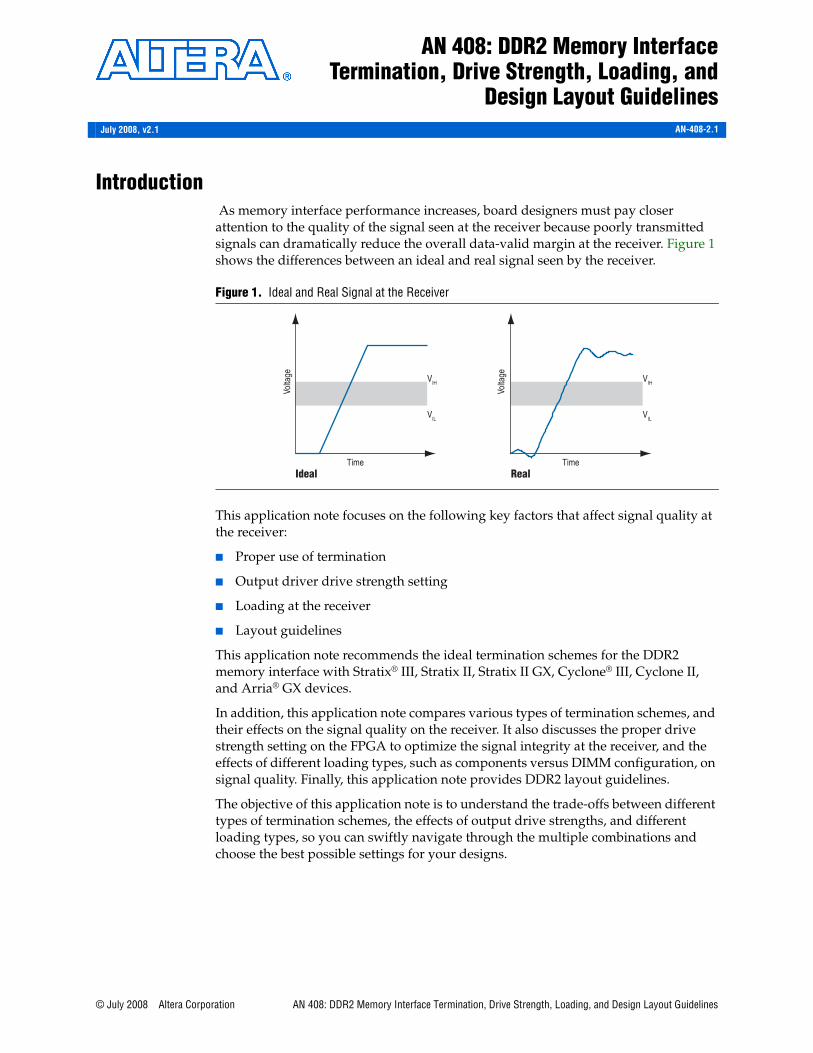
AN-408-2.1Introduction As memory interface performance increases, board designers must pay closer attention to the quality of the signal seen at the receiver because poorly transmitted signals can dramatically reduce the overall data-valid margin at the receiver. Figure 1 shows the differences between an ideal and real signal seen by the receiver.
This application note focuses on the following key factors that affect signal quality at the receiver:
■ Proper use of termination
■ Output driver drive strength setting
■ Loading at the receiver
■ Layout guidelines
This application note recommends the ideal termination schemes for the DDR2 memory interface with Stratix® III, Stratix II, Stratix II GX, Cyclone® III, Cyclone II, and Arria® GX devices.
In addition, this application note compares various types of termination schemes, and their effects on the signal quality on the receiver. It also discusses the proper drive strength setting on the FPGA to optimize the signal integrity at the receiver, and the effects of different loading types, such as components versus DIMM configuration, on signal quality. Finally, this application note provides DDR2 layout guidelines.
The objective of this application note is to understand the trade-offs between different types of termination schemes, the effects of output drive strengths, and different loading types, so you can swiftly navigate through the multiple combinations and choose the best possible settings for your designs.
Figure 1. Ideal and Real Signal at the Receiver
Ideal Real
Volta
ge
Volta
geVIH VIH
VIL VIL
Time Time
8: DDR2 Memory Interface Termination, Drive Strength, Loading, and Design Layout Guidelines
Page 2 Board Termination
Board TerminationIn board-level design, you can use a variety of termination schemes. DDR2 adheres to the JEDEC standard of governing Stub-Series Terminated Logic (SSTL), JESD8-15a, which includes four different termination schemes.
Two commonly used termination schemes of SSTL are:
■ Single parallel terminated output load with or without series resistors (Class I, as stated in JESD8-15a)
■ Double parallel terminated output load with or without series resistors (Class II, as stated in JESD8-15a)
Depending on the type of signals you choose, you can use either termination scheme. Also, depending on your design’s FPGA and SDRAM memory devices, you may choose external or internal termination schemes.
With the ever-increasing requirements to reduce system cost and simplify printed circuit board (PCB) layout design, you may choose not to have any parallel termination on the transmission line, and use point-to-point connections between the memory interface and the memory. In this case, you may take advantage of internal termination schemes such as On-Chip Termination (OCT) on the FPGA side and On-Die Termination (ODT) on the SDRAM side when it is offered on your chosen device.
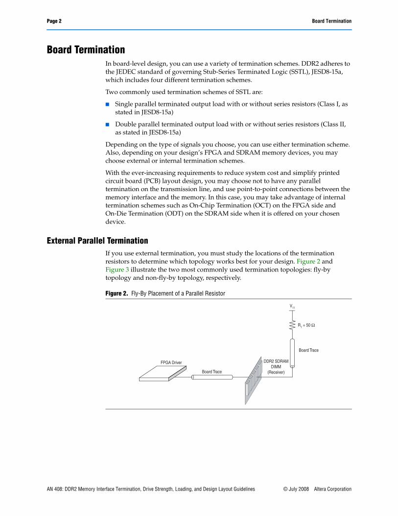
External Parallel TerminationIf you use external termination, you must study the locations of the termination resistors to determine which topology works best for your design. Figure 2 and Figure 3 illustrate the two most commonly used termination topologies: fly-by topology and non-fly-by topology, respectively.
Figure 2. Fly-By Placement of a Parallel Resistor
FPGA Driver
Board Trace
DDR2 SDRAMDIMM
(Receiver)
Board Trace
RT = 50 Ω
VTT
AN 408: DDR2 Memory Interface Termination, Drive Strength, Loading, and Design Layout Guidelines © July 2008 Altera Corporation
Board Termination Page 3
With fly-by topology (shown in Figure 2), you place the parallel termination resistor after the receiver. This termination placement resolves the undesirable unterminated stub found in the non-fly-by topology. However, using this topology can be costly and complicate routing. The Stratix II Memory Board 2 uses the fly-by topology for the parallel terminating resistors placement. The Stratix II Memory Board 2 is a memory test board available only within Altera for the purpose of testing and validating Altera’s memory interface.
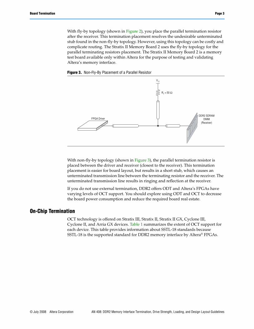
With non-fly-by topology (shown in Figure 3), the parallel termination resistor is placed between the driver and receiver (closest to the receiver). This termination placement is easier for board layout, but results in a short stub, which causes an unterminated transmission line between the terminating resistor and the receiver. The unterminated transmission line results in ringing and reflection at the receiver.
If you do not use external termination, DDR2 offers ODT and Altera’s FPGAs have varying levels of OCT support. You should explore using ODT and OCT to decrease the board power consumption and reduce the required board real estate.
On-Chip TerminationOCT technology is offered on Stratix III, Stratix II, Stratix II GX, Cyclone III, Cyclone II, and Arria GX devices. Table 1 summarizes the extent of OCT support for each device. This table provides information about SSTL-18 standards because SSTL-18 is the supported standard for DDR2 memory interface by Altera® FPGAs.
Figure 3. Non-Fly-By Placement of a Parallel Resistor
FPGA DriverDDR2 SDRAM
DIMM(Receiver)
RT = 50 Ω
VTT
© July 2008 Altera Corporation AN 408: DDR2 Memory Interface Termination, Drive Strength, Loading, and Design Layout Guidelines
Page 4 Board Termination
On-Chip Series (Rs) termination is supported only on output and bidirectional buffers. The value of Rs with calibration is calibrated against a 25-Ω resistor for class II and 50-Ω resistor for class I connected to Rup and Rdn pins and adjusted to ± 1% of 25 Ω or 50 Ω. On-Chip Parallel (Rt) termination is supported only on inputs and bidirectional buffers. The value of Rt is calibrated against 100 Ω connected to the Rup and Rdn pins. Calibration occurs at the end of device configuration. Dynamic OCT is supported only on bidirectional I/O buffers.
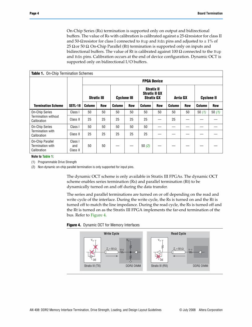
The dynamic OCT scheme is only available in Stratix III FPGAs. The dynamic OCT scheme enables series termination (Rs) and parallel termination (Rt) to be dynamically turned on and off during the data transfer.
The series and parallel terminations are turned on or off depending on the read and write cycle of the interface. During the write cycle, the Rs is turned on and the Rt is turned off to match the line impedance. During the read cycle, the Rs is turned off and the Rt is turned on as the Stratix III FPGA implements the far-end termination of the bus. Refer to Figure 4.
Table 1. On-Chip Termination Schemes
Termination Scheme SSTL-18
FPGA Device
Stratix III Cyclone III
Stratix IIStratix II GXStratix GX Arria GX Cyclone II
Column Row Column Row Column Row Column Row Column Row
On-Chip Series Termination without Calibration
Class I 50 50 50 50 50 50 50 50 50 (1) 50 (1)
Class II 25 25 25 25 25 — 25 — — —
On-Chip Series Termination with Calibration
Class I 50 50 50 50 50 — — — — —
Class II 25 25 25 25 25 — — — — —
On-Chip Parallel Termination with Calibration
Class Iand
Class II50 50 — — 50 (2) — — — — —
Note to Table 1:
(1) Programmable Drive Strength(2) Non-dynamic on-chip parallel termination is only supported for input pins.
Figure 4. Dynamic OCT for Memory Interfaces
Stratix III (TX) DDR2 DIMM Stratix III (RX) DDR2 DIMM
Write Cycle Read Cycle
OEOE
VTT VTT VTT
Z0 = 50 Ω Z0 = 50 Ω22 Ω 22 Ω22 Ω
AN 408: DDR2 Memory Interface Termination, Drive Strength, Loading, and Design Layout Guidelines © July 2008 Altera Corporation
Board Termination Page 5
Simulation and Measurement SetupTo study the different types of termination schemes properly, the simulation and measurement setups described in this application note use two options:
■ Altera Stratix III FPGA interfacing with a 400-MHz DDR2 SDRAM unbuffered DIMM
■ Altera Stratix II FPGA interfacing with a 267-MHz DDR2 SDRAM unbuffered DIMM
1 The maximum achievable frequency in Straitx II DDR2 SDRAM is 333 MHz. The 267 MHz frequency is due to the device speed grade mounted on the Stratix II Memory Board 2 board.
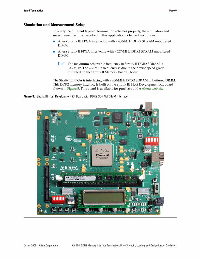
The Stratix III FPGA is interfacing with a 400-MHz DDR2 SDRAM unbuffered DIMM. This DDR2 memory interface is built on the Stratix III Host Development Kit Board shown in Figure 5. This board is available for purchase at the Altera web site.
Figure 5. Stratix III Host Development Kit Board with DDR2 SDRAM DIMM Interface
© July 2008 Altera Corporation AN 408: DDR2 Memory Interface Termination, Drive Strength, Loading, and Design Layout Guidelines
Page 6 Board Termination
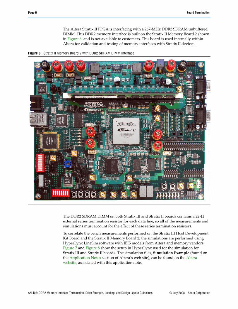
The Altera Stratix II FPGA is interfacing with a 267-MHz DDR2 SDRAM unbuffered DIMM. This DDR2 memory interface is built on the Stratix II Memory Board 2 shown in Figure 6. and is not available to customers. This board is used internally within Altera for validation and testing of memory interfaces with Stratix II devices.
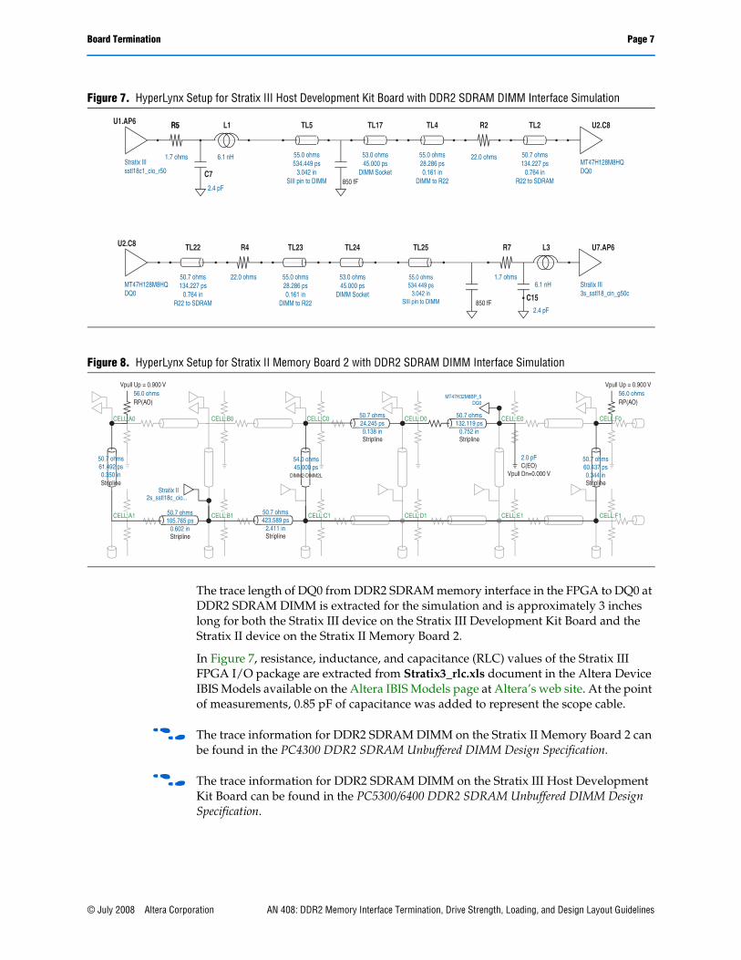
The DDR2 SDRAM DIMM on both Stratix III and Stratix II boards contains a 22-Ω external series termination resistor for each data line, so all of the measurements and simulations must account for the effect of these series termination resistors.
To correlate the bench measurements performed on the Stratix III Host Development Kit Board and the Stratix II Memory Board 2, the simulations are performed using HyperLynx LineSim software with IBIS models from Altera and memory vendors. Figure 7 and Figure 8 show the setup in HyperLynx used for the simulation for Stratix III and Stratix II boards. The simulation files, Simulation Example (found on the Application Notes section of Altera’s web site), can be found on the Altera website, associated with this application note.
Figure 6. Stratix II Memory Board 2 with DDR2 SDRAM DIMM Interface
AN 408: DDR2 Memory Interface Termination, Drive Strength, Loading, and Design Layout Guidelines © July 2008 Altera Corporation
Board Termination Page 7
The trace length of DQ0 from DDR2 SDRAM memory interface in the FPGA to DQ0 at DDR2 SDRAM DIMM is extracted for the simulation and is approximately 3 inches long for both the Stratix III device on the Stratix III Development Kit Board and the Stratix II device on the Stratix II Memory Board 2.
In Figure 7, resistance, inductance, and capacitance (RLC) values of the Stratix III FPGA I/O package are extracted from Stratix3_rlc.xls document in the Altera Device IBIS Models available on the Altera IBIS Models page at Altera’s web site. At the point of measurements, 0.85 pF of capacitance was added to represent the scope cable.
f The trace information for DDR2 SDRAM DIMM on the Stratix II Memory Board 2 can be found in the PC4300 DDR2 SDRAM Unbuffered DIMM Design Specification.
f The trace information for DDR2 SDRAM DIMM on the Stratix III Host Development Kit Board can be found in the PC5300/6400 DDR2 SDRAM Unbuffered DIMM Design Specification.
Figure 7. HyperLynx Setup for Stratix III Host Development Kit Board with DDR2 SDRAM DIMM Interface Simulation
Stratix IIIsstl18c1_cio_r50
1.7 ohms 6.1 nH
2.4 pF
C7850 fF
L1R5R5U1.AP6 TL5 TL17 TL4 R2 TL2 U2.C8
U2.C8 TL22 R4 TL23 TL24 TL25 R7 L3 U7.AP6
55.0 ohms534.449 ps
3.042 inSIII pin to DIMM
53.0 ohms45.000 ps
DIMM Socket
55.0 ohms28.286 ps0.161 in
DIMM to R22
22.0 ohms 50.7 ohms134.227 ps
0.764 inR22 to SDRAM
MT47H128M8HQDQ0
MT47H128M8HQDQ0
50.7 ohms134.227 ps
0.764 inR22 to SDRAM
22.0 ohms 55.0 ohms28.286 ps0.161 in
DIMM to R22
53.0 ohms45.000 ps
DIMM Socket
55.0 ohms534.449 ps
3.042 inSIII pin to DIMM
1.7 ohms
C15
6.1 nH
2.4 pF
Stratix III3s_sstl18_cin_g50c
850 fF
Figure 8. HyperLynx Setup for Stratix II Memory Board 2 with DDR2 SDRAM DIMM Interface Simulation
Vpull Up = 0.900 V56.0 ohmsRP(AO)
CELL:A0
CELL:A1
50.7 ohms61.492 ps0.350 inStripline
50.7 ohms105.765 ps
0.602 inStripline
2s_sstl18c_cio...Stratix II
CELL:B1
CELL:B0 CELL:C0
50.7 ohms423.589 ps
2.411 inStripline
CELL:C1
54.0 ohms45.000 ps
DIMM2-DIMM2L
50.7 ohms24.245 ps0.138 inStripline
CELL:D1 CELL:E1 CELL:F1
CELL:F0CELL:E0CELL:D0 50.7 ohms132.119 ps
0.752 inStripline
MT47H32M8BP_5DQ0
2.0 pFC(EO)
Vpull Dn=0.000 V
Vpull Up = 0.900 V56.0 ohmsRP(AO)
50.7 ohms60.437 ps0.344 inStripline
© July 2008 Altera Corporation AN 408: DDR2 Memory Interface Termination, Drive Strength, Loading, and Design Layout Guidelines
Page 8 Board Termination
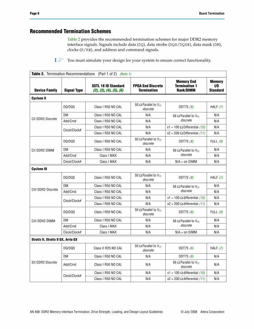
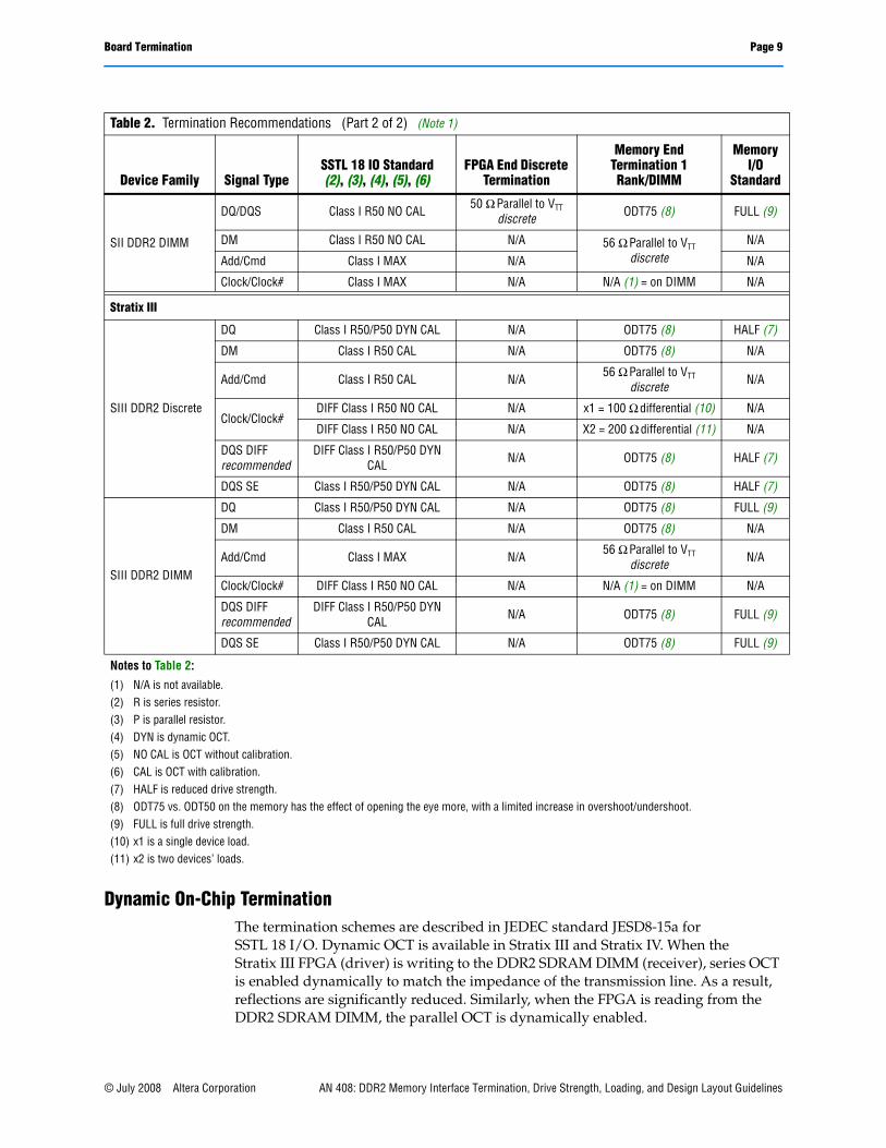
Recommended Termination SchemesTable 2 provides the recommended termination schemes for major DDR2 memory interface signals. Signals include data (DQ), data strobe (DQS/DQS#), data mask (DM), clocks (K/K#), and address and command signals.
1 You must simulate your design for your system to ensure correct functionality.
Table 2. Termination Recommendations (Part 1 of 2) (Note 1)
Device Family Signal TypeSSTL 18 IO Standard(2), (3), (4), (5), (6)
FPGA End Discrete Termination
Memory End Termination 1 Rank/DIMM
Memory I/O
Standard
Cyclone II
CII DDR2 Discrete
DQ/DQS Class I R50 NO CAL 50 Ω Parallel to VTT discrete
ODT75 (8) HALF (7)
DM Class I R50 NO CAL N/A 56 Ω Parallel to VTT discrete
N/A
Add/Cmd Class I R50 NO CAL N/A N/A
Clock/Clock#Class I R50 NO CAL N/A x1 = 100 Ω Differential (10) N/A
Class I R50 NO CAL N/A x2 = 200 Ω Differential (11) N/A
CII DDR2 DIMM
DQ/DQS Class I R50 NO CAL 50 Ω Parallel to VTT discrete
ODT75 (8) FULL (9)
DM Class I R50 NO CAL N/A 56 Ω Parallel to VTT discrete
N/A
Add/Cmd Class I MAX N/A N/A
Clock/Clock# Class I MAX N/A N/A = on DIMM N/A
Cyclone III
CIII DDR2 Discrete
DQ/DQS Class I R50 NO CAL50 Ω Parallel to VTT
discrete ODT75 (8) HALF (7)
DM Class I R50 NO CAL N/A 56 Ω Parallel to VTT discrete
N/A
Add/Cmd Class I R50 NO CAL N/A N/A
Clock/Clock#Class I R50 NO CAL N/A x1 = 100 Ω differential (10) N/A
Class I R50 NO CAL N/A x2 = 200 Ω differential (11) N/A
CIII DDR2 DIMM
DQ/DQS Class I R50 NO CAL50 Ω Parallel to VTT
discrete ODT75 (8) FULL (9)
DM Class I R50 NO CAL N/A 56 Ω Parallel to VTT discrete
N/A
Add/Cmd Class I MAX N/A N/A
Clock/Clock# Class I MAX N/A N/A = on DIMM N/A
Stratix II, Stratix II GX, Arria GX
SII DDR2 Discrete
DQ/DQS Class II R25 NO CAL50 Ω Parallel to VTT
discrete ODT75 (8) HALF (7)
DM Class I R50 NO CAL N/A ODT75 (8) N/A
Add/Cmd Class I R50 NO CAL N/A 56 Ω Parallel to VTT
discreteN/A
Clock/Clock#Class I R50 NO CAL N/A x1 = 100 Ω differential (10) N/A
Class I R50 NO CAL N/A x2 = 200 Ω differential (11) N/A
AN 408: DDR2 Memory Interface Termination, Drive Strength, Loading, and Design Layout Guidelines © July 2008 Altera Corporation
Board Termination Page 9
Dynamic On-Chip TerminationThe termination schemes are described in JEDEC standard JESD8-15a for SSTL 18 I/O. Dynamic OCT is available in Stratix III and Stratix IV. When the Stratix III FPGA (driver) is writing to the DDR2 SDRAM DIMM (receiver), series OCT is enabled dynamically to match the impedance of the transmission line. As a result, reflections are significantly reduced. Similarly, when the FPGA is reading from the DDR2 SDRAM DIMM, the parallel OCT is dynamically enabled.
SII DDR2 DIMM
DQ/DQS Class I R50 NO CAL50 Ω Parallel to VTT
discrete ODT75 (8) FULL (9)
DM Class I R50 NO CAL N/A 56 Ω Parallel to VTT discrete
N/A
Add/Cmd Class I MAX N/A N/A
Clock/Clock# Class I MAX N/A N/A (1) = on DIMM N/A
Stratix III
SIII DDR2 Discrete
DQ Class I R50/P50 DYN CAL N/A ODT75 (8) HALF (7)
DM Class I R50 CAL N/A ODT75 (8) N/A
Add/Cmd Class I R50 CAL N/A 56 Ω Parallel to VTT discrete
N/A
Clock/Clock#DIFF Class I R50 NO CAL N/A x1 = 100 Ω differential (10) N/A
DIFF Class I R50 NO CAL N/A X2 = 200 Ω differential (11) N/A
DQS DIFFrecommended
DIFF Class I R50/P50 DYN CAL
N/A ODT75 (8) HALF (7)
DQS SE Class I R50/P50 DYN CAL N/A ODT75 (8) HALF (7)
SIII DDR2 DIMM
DQ Class I R50/P50 DYN CAL N/A ODT75 (8) FULL (9)
DM Class I R50 CAL N/A ODT75 (8) N/A
Add/Cmd Class I MAX N/A56 Ω Parallel to VTT
discrete N/A
Clock/Clock# DIFF Class I R50 NO CAL N/A N/A (1) = on DIMM N/A
DQS DIFFrecommended
DIFF Class I R50/P50 DYN CAL
N/A ODT75 (8) FULL (9)
DQS SE Class I R50/P50 DYN CAL N/A ODT75 (8) FULL (9)
Notes to Table 2:
(1) N/A is not available.(2) R is series resistor.(3) P is parallel resistor.(4) DYN is dynamic OCT.(5) NO CAL is OCT without calibration.(6) CAL is OCT with calibration.(7) HALF is reduced drive strength.(8) ODT75 vs. ODT50 on the memory has the effect of opening the eye more, with a limited increase in overshoot/undershoot.(9) FULL is full drive strength.(10) x1 is a single device load.(11) x2 is two devices’ loads.
Table 2. Termination Recommendations (Part 2 of 2) (Note 1)
Device Family Signal TypeSSTL 18 IO Standard(2), (3), (4), (5), (6)
FPGA End Discrete Termination
Memory End Termination 1 Rank/DIMM
Memory I/O
Standard
© July 2008 Altera Corporation AN 408: DDR2 Memory Interface Termination, Drive Strength, Loading, and Design Layout Guidelines
Page 10 Board Termination
f For information about setting the proper value for termination resistors, refer to the Stratix III Device I/O Features chapter in the Stratix III Device Handbook.
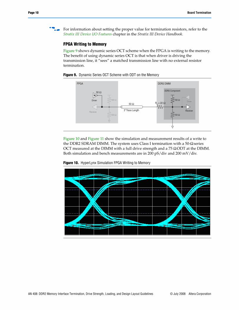
FPGA Writing to MemoryFigure 9 shows dynamic series OCT scheme when the FPGA is writing to the memory. The benefit of using dynamic series OCT is that when driver is driving the transmission line, it “sees” a matched transmission line with no external resistor termination.
Figure 10 and Figure 11 show the simulation and measurement results of a write to the DDR2 SDRAM DIMM. The system uses Class I termination with a 50-Ω series OCT measured at the DIMM with a full drive strength and a 75 Ω ODT at the DIMM. Both simulation and bench measurements are in 200 pS/div and 200 mV/div.
Figure 9. Dynamic Series OCT Scheme with ODT on the Memory
Figure 10. HyperLynx Simulation FPGA Writing to Memory
FPGA DDR2 DIMM
DDR2 Component
RS = 22 ΩDriver Driver
Receiver
50 Ω
3” Trace Length Receiver
50 Ω
150 Ω
150 Ω
100 Ω
100 Ω
AN 408: DDR2 Memory Interface Termination, Drive Strength, Loading, and Design Layout Guidelines © July 2008 Altera Corporation
Board Termination Page 11
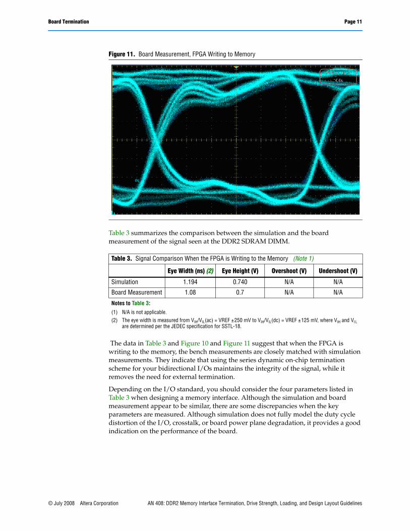
Table 3 summarizes the comparison between the simulation and the board measurement of the signal seen at the DDR2 SDRAM DIMM.
The data in Table 3 and Figure 10 and Figure 11 suggest that when the FPGA is writing to the memory, the bench measurements are closely matched with simulation measurements. They indicate that using the series dynamic on-chip termination scheme for your bidirectional I/Os maintains the integrity of the signal, while it removes the need for external termination.
Depending on the I/O standard, you should consider the four parameters listed in Table 3 when designing a memory interface. Although the simulation and board measurement appear to be similar, there are some discrepancies when the key parameters are measured. Although simulation does not fully model the duty cycle distortion of the I/O, crosstalk, or board power plane degradation, it provides a good indication on the performance of the board.
Figure 11. Board Measurement, FPGA Writing to Memory
Table 3. Signal Comparison When the FPGA is Writing to the Memory (Note 1)
Eye Width (ns) (2) Eye Height (V) Overshoot (V) Undershoot (V)
Simulation 1.194 0.740 N/A N/A
Board Measurement 1.08 0.7 N/A N/A
Notes to Table 3:
(1) N/A is not applicable.(2) The eye width is measured from VIH/VIL(ac) = VREF ±250 mV to VIH/VIL(dc) = VREF ±125 mV, where VIH and VI L
are determined per the JEDEC specification for SSTL-18.
© July 2008 Altera Corporation AN 408: DDR2 Memory Interface Termination, Drive Strength, Loading, and Design Layout Guidelines
Page 12 Board Termination
For memory interfaces, the eye width is important when determining if there is a sufficient window to correctly capture the data. Regarding the eye height, even though most memory interfaces use voltage-referenced I/O standards (in this case, SSTL-18), as long as there is sufficient eye opening below and above VIL and VIH, there should be enough margin to correctly capture the data. However, because effects such as crosstalk are not taken into account, it is critical to design a system to achieve the optimum eye height, because it impacts the overall margin of a system with a memory interface.
f Refer to the memory vendors when determining the over- and undershoot. They typically specify a maximum limit on the input voltage to prevent reliability issues.
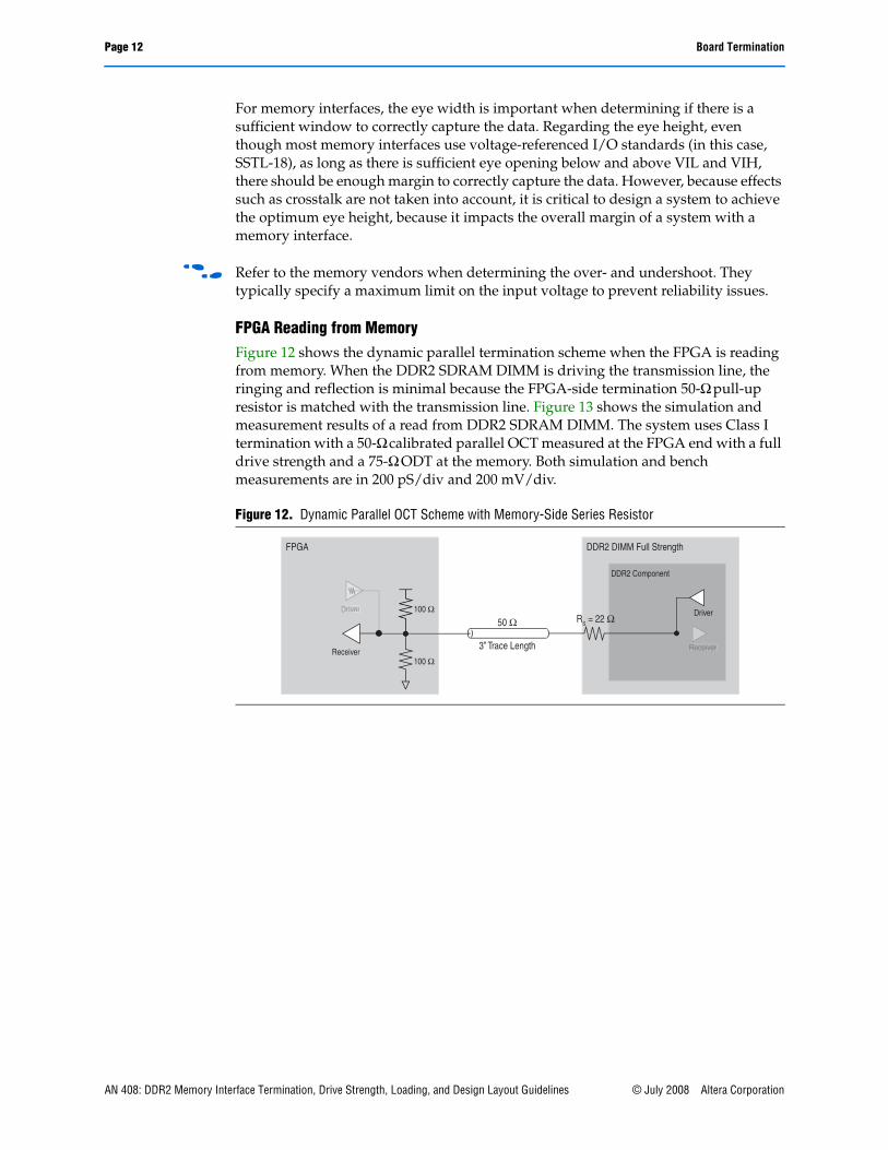
FPGA Reading from MemoryFigure 12 shows the dynamic parallel termination scheme when the FPGA is reading from memory. When the DDR2 SDRAM DIMM is driving the transmission line, the ringing and reflection is minimal because the FPGA-side termination 50-Ω pull-up resistor is matched with the transmission line. Figure 13 shows the simulation and measurement results of a read from DDR2 SDRAM DIMM. The system uses Class I termination with a 50-Ω calibrated parallel OCT measured at the FPGA end with a full drive strength and a 75-Ω ODT at the memory. Both simulation and bench measurements are in 200 pS/div and 200 mV/div.
Figure 12. Dynamic Parallel OCT Scheme with Memory-Side Series Resistor
FPGA DDR2 DIMM Full Strength
DDR2 Component
RS = 22 ΩDriver Driver
Receiver
50 Ω
3” Trace Length Receiver
100 Ω
100 Ω
AN 408: DDR2 Memory Interface Termination, Drive Strength, Loading, and Design Layout Guidelines © July 2008 Altera Corporation
Board Termination Page 13
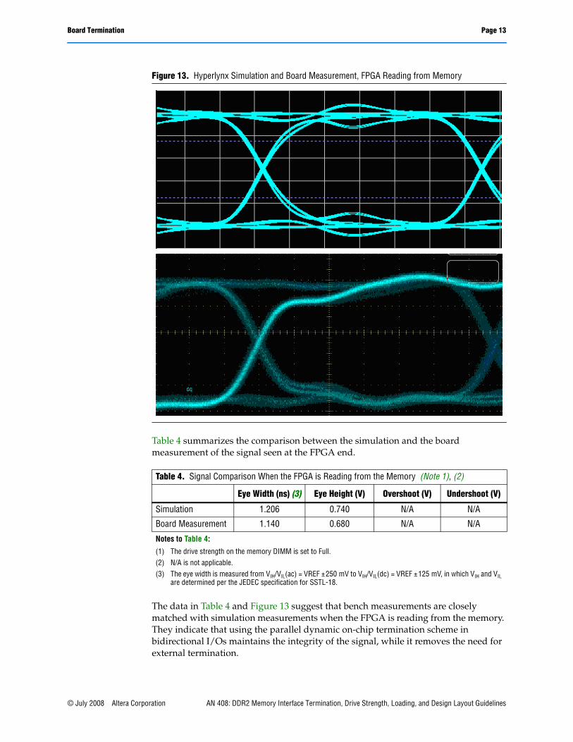
Table 4 summarizes the comparison between the simulation and the board measurement of the signal seen at the FPGA end.
The data in Table 4 and Figure 13 suggest that bench measurements are closely matched with simulation measurements when the FPGA is reading from the memory. They indicate that using the parallel dynamic on-chip termination scheme in bidirectional I/Os maintains the integrity of the signal, while it removes the need for external termination.
Figure 13. Hyperlynx Simulation and Board Measurement, FPGA Reading from Memory
Table 4. Signal Comparison When the FPGA is Reading from the Memory (Note 1), (2)
Eye Width (ns) (3) Eye Height (V) Overshoot (V) Undershoot (V)
Simulation 1.206 0.740 N/A N/A
Board Measurement 1.140 0.680 N/A N/A
Notes to Table 4:
(1) The drive strength on the memory DIMM is set to Full.(2) N/A is not applicable.(3) The eye width is measured from VIH/VIL(ac) = VREF ±250 mV to VIH/VIL(dc) = VREF ±125 mV, in which VIH and VIL
are determined per the JEDEC specification for SSTL-18.
© July 2008 Altera Corporation AN 408: DDR2 Memory Interface Termination, Drive Strength, Loading, and Design Layout Guidelines
Page 14 Board Termination
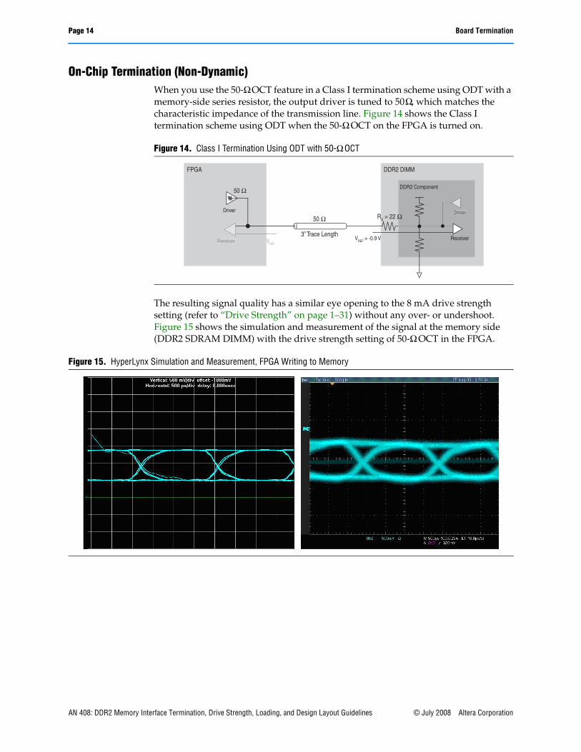
On-Chip Termination (Non-Dynamic)When you use the 50-Ω OCT feature in a Class I termination scheme using ODT with a memory-side series resistor, the output driver is tuned to 50Ω, which matches the characteristic impedance of the transmission line. Figure 14 shows the Class I termination scheme using ODT when the 50-Ω OCT on the FPGA is turned on.
The resulting signal quality has a similar eye opening to the 8 mA drive strength setting (refer to “Drive Strength” on page 1–31) without any over- or undershoot. Figure 15 shows the simulation and measurement of the signal at the memory side (DDR2 SDRAM DIMM) with the drive strength setting of 50-Ω OCT in the FPGA.
Figure 14. Class I Termination Using ODT with 50-Ω OCT
FPGA DDR2 DIMM
DDR2 Component
RS = 22 Ω
VREF = -0.9 V
Driver Driver
Receiver
50 Ω
3” Trace LengthReceiverVVREF
50 Ω
Figure 15. HyperLynx Simulation and Measurement, FPGA Writing to Memory
AN 408: DDR2 Memory Interface Termination, Drive Strength, Loading, and Design Layout Guidelines © July 2008 Altera Corporation
Board Termination Page 15
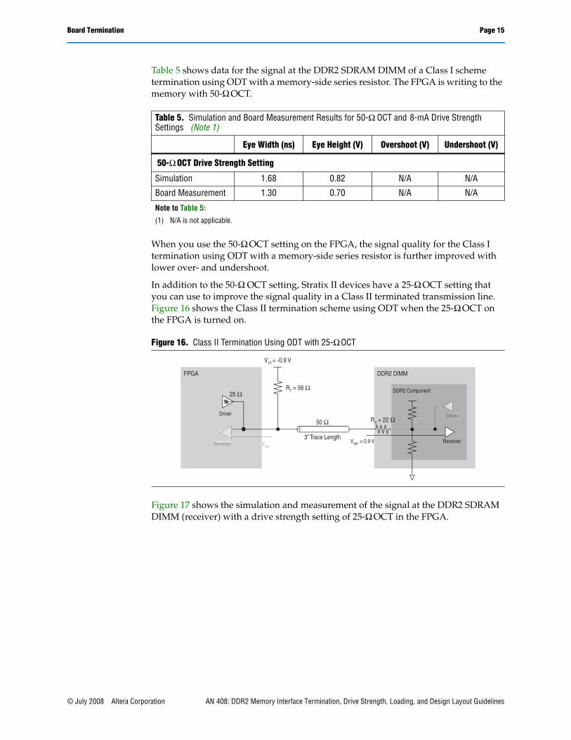
Table 5 shows data for the signal at the DDR2 SDRAM DIMM of a Class I scheme termination using ODT with a memory-side series resistor. The FPGA is writing to the memory with 50-Ω OCT.
When you use the 50-Ω OCT setting on the FPGA, the signal quality for the Class I termination using ODT with a memory-side series resistor is further improved with lower over- and undershoot.
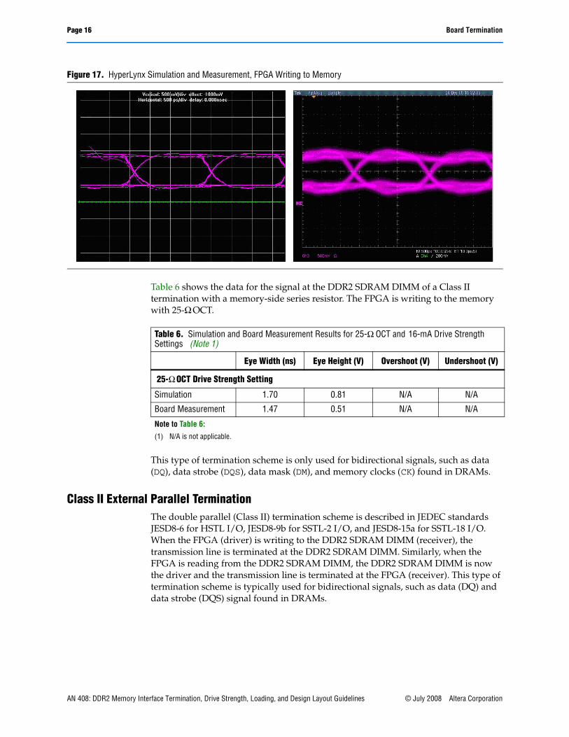
In addition to the 50-Ω OCT setting, Stratix II devices have a 25-Ω OCT setting that you can use to improve the signal quality in a Class II terminated transmission line. Figure 16 shows the Class II termination scheme using ODT when the 25-Ω OCT on the FPGA is turned on.
Figure 17 shows the simulation and measurement of the signal at the DDR2 SDRAM DIMM (receiver) with a drive strength setting of 25-Ω OCT in the FPGA.
Table 5. Simulation and Board Measurement Results for 50-Ω OCT and 8-mA Drive Strength Settings (Note 1)
Eye Width (ns) Eye Height (V) Overshoot (V) Undershoot (V)
50-Ω OCT Drive Strength Setting
Simulation 1.68 0.82 N/A N/A
Board Measurement 1.30 0.70 N/A N/A
Note to Table 5:(1) N/A is not applicable.
Figure 16. Class II Termination Using ODT with 25-Ω OCT
DDR2 DIMM
DDR2 Component
RS = 22 Ω
VREF = 0.9 V
Driver50 Ω
3” Trace LengthReceiver
RT = 56 Ω
VTT = -0.9 V
FPGA
Driver
Receiver VVREF
25 Ω
© July 2008 Altera Corporation AN 408: DDR2 Memory Interface Termination, Drive Strength, Loading, and Design Layout Guidelines
Page 16 Board Termination
Table 6 shows the data for the signal at the DDR2 SDRAM DIMM of a Class II termination with a memory-side series resistor. The FPGA is writing to the memory with 25-Ω OCT.
This type of termination scheme is only used for bidirectional signals, such as data (DQ), data strobe (DQS), data mask (DM), and memory clocks (CK) found in DRAMs.
Class II External Parallel TerminationThe double parallel (Class II) termination scheme is described in JEDEC standards JESD8-6 for HSTL I/O, JESD8-9b for SSTL-2 I/O, and JESD8-15a for SSTL-18 I/O. When the FPGA (driver) is writing to the DDR2 SDRAM DIMM (receiver), the transmission line is terminated at the DDR2 SDRAM DIMM. Similarly, when the FPGA is reading from the DDR2 SDRAM DIMM, the DDR2 SDRAM DIMM is now the driver and the transmission line is terminated at the FPGA (receiver). This type of termination scheme is typically used for bidirectional signals, such as data (DQ) and data strobe (DQS) signal found in DRAMs.
Figure 17. HyperLynx Simulation and Measurement, FPGA Writing to Memory
Table 6. Simulation and Board Measurement Results for 25-Ω OCT and 16-mA Drive Strength Settings (Note 1)
Eye Width (ns) Eye Height (V) Overshoot (V) Undershoot (V)
25-Ω OCT Drive Strength Setting
Simulation 1.70 0.81 N/A N/A
Board Measurement 1.47 0.51 N/A N/A
Note to Table 6:(1) N/A is not applicable.
AN 408: DDR2 Memory Interface Termination, Drive Strength, Loading, and Design Layout Guidelines © July 2008 Altera Corporation
Board Termination Page 17
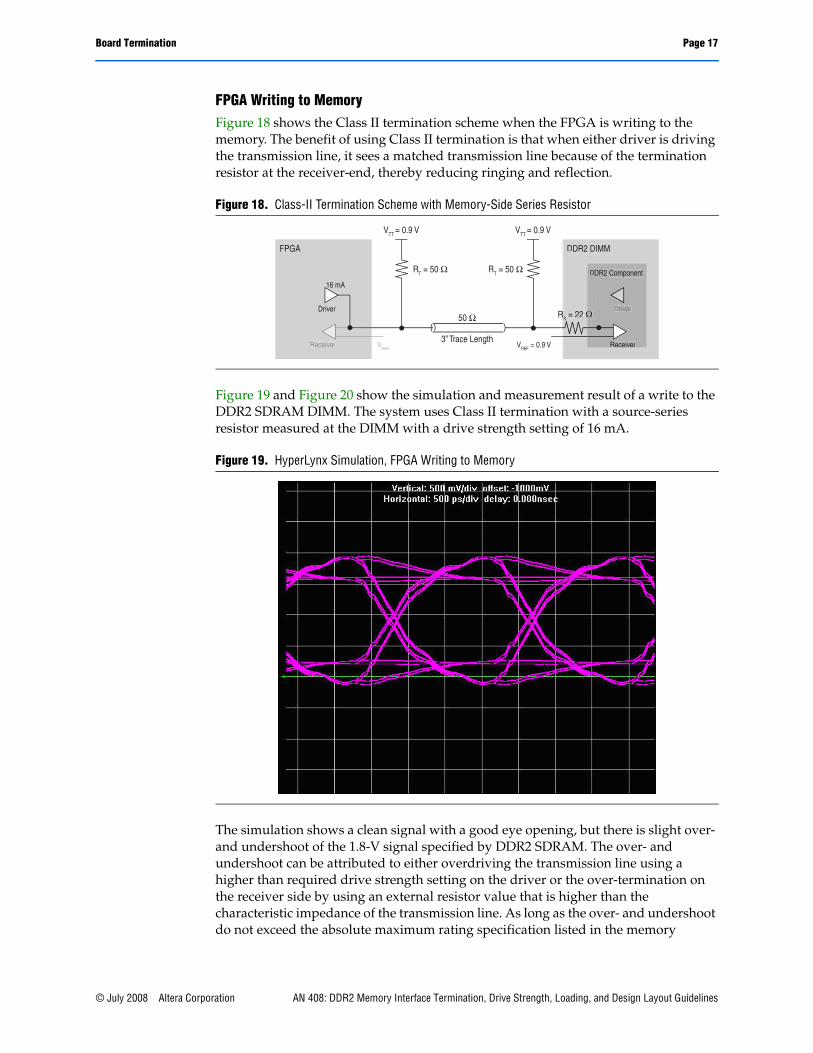
FPGA Writing to MemoryFigure 18 shows the Class II termination scheme when the FPGA is writing to the memory. The benefit of using Class II termination is that when either driver is driving the transmission line, it sees a matched transmission line because of the termination resistor at the receiver-end, thereby reducing ringing and reflection.
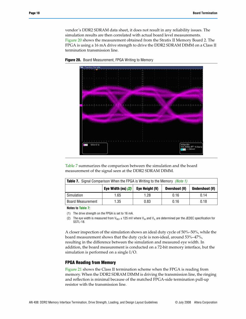
Figure 19 and Figure 20 show the simulation and measurement result of a write to the DDR2 SDRAM DIMM. The system uses Class II termination with a source-series resistor measured at the DIMM with a drive strength setting of 16 mA.
The simulation shows a clean signal with a good eye opening, but there is slight over- and undershoot of the 1.8-V signal specified by DDR2 SDRAM. The over- and undershoot can be attributed to either overdriving the transmission line using a higher than required drive strength setting on the driver or the over-termination on the receiver side by using an external resistor value that is higher than the characteristic impedance of the transmission line. As long as the over- and undershoot do not exceed the absolute maximum rating specification listed in the memory
Figure 18. Class-II Termination Scheme with Memory-Side Series Resistor
Figure 19. HyperLynx Simulation, FPGA Writing to Memory
RT = 50 Ω
VTT = 0.9 V
RT = 50 Ω
VTT = 0.9 V
FPGA DDR2 DIMM
DDR2 Component
RS = 22 Ω
VREF = 0.9 VVREF Receiver
Driver
Receiver
16 mA
50 Ω
3” Trace Length
DDR2 DIMM
S = 22 ΩR
DDR2 Component
Ω
Receiver
Ω
Receiver
Driver
© July 2008 Altera Corporation AN 408: DDR2 Memory Interface Termination, Drive Strength, Loading, and Design Layout Guidelines
Page 18 Board Termination
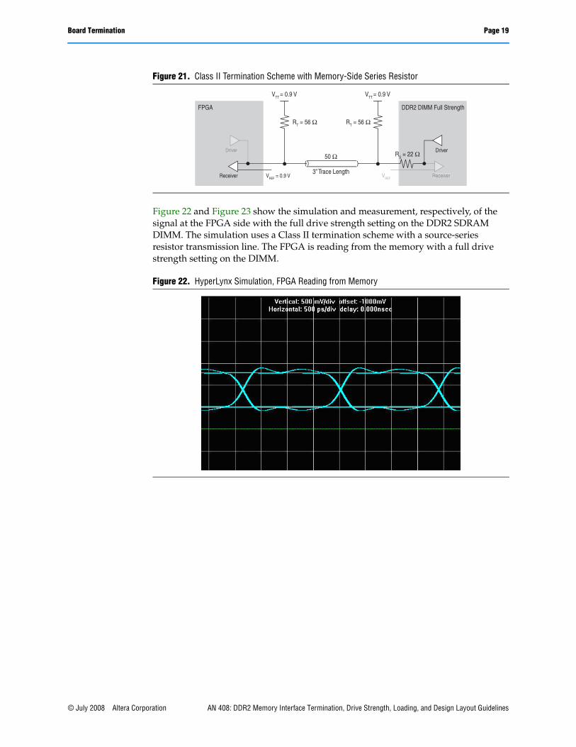
vendor’s DDR2 SDRAM data sheet, it does not result in any reliability issues. The simulation results are then correlated with actual board level measurements. Figure 20 shows the measurement obtained from the Stratix II Memory Board 2. The FPGA is using a 16 mA drive strength to drive the DDR2 SDRAM DIMM on a Class II termination transmission line.
Table 7 summarizes the comparison between the simulation and the board measurement of the signal seen at the DDR2 SDRAM DIMM.
A closer inspection of the simulation shows an ideal duty cycle of 50%–50%, while the board measurement shows that the duty cycle is non-ideal, around 53%–47%, resulting in the difference between the simulation and measured eye width. In addition, the board measurement is conducted on a 72-bit memory interface, but the simulation is performed on a single I/O.
FPGA Reading from MemoryFigure 21 shows the Class II termination scheme when the FPGA is reading from memory. When the DDR2 SDRAM DIMM is driving the transmission line, the ringing and reflection is minimal because of the matched FPGA-side termination pull-up resistor with the transmission line.
Figure 20. Board Measurement, FPGA Writing to Memory
Table 7. Signal Comparison When the FPGA is Writing to the Memory (Note 1)
Eye Width (ns) (2) Eye Height (V) Overshoot (V) Undershoot (V)
Simulation 1.65 1.28 0.16 0.14
Board Measurement 1.35 0.83 0.16 0.18
Notes to Table 7:
(1) The drive strength on the FPGA is set to 16 mA.(2) The eye width is measured from VREF ± 125 mV where VIH and VIL are determined per the JEDEC specification for
SSTL-18.
AN 408: DDR2 Memory Interface Termination, Drive Strength, Loading, and Design Layout Guidelines © July 2008 Altera Corporation
Board Termination Page 19
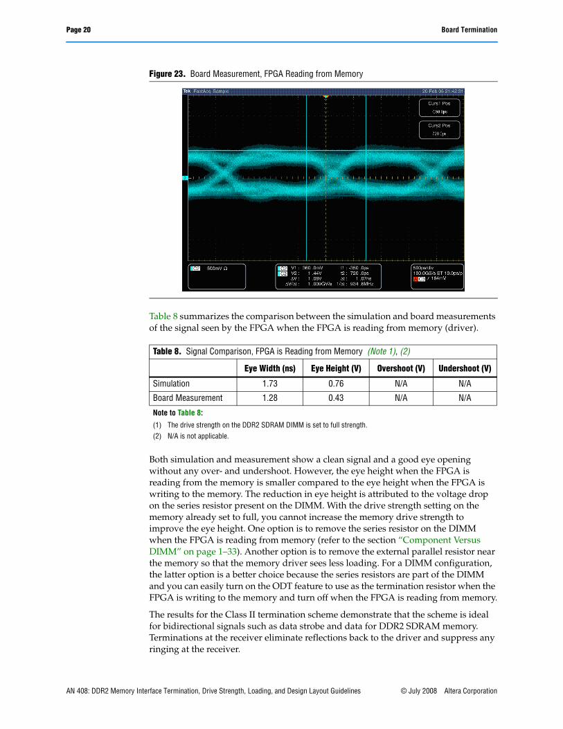
Figure 22 and Figure 23 show the simulation and measurement, respectively, of the signal at the FPGA side with the full drive strength setting on the DDR2 SDRAM DIMM. The simulation uses a Class II termination scheme with a source-series resistor transmission line. The FPGA is reading from the memory with a full drive strength setting on the DIMM.
Figure 21. Class II Termination Scheme with Memory-Side Series Resistor
Figure 22. HyperLynx Simulation, FPGA Reading from Memory
RT = 56 Ω
VTT = 0.9 V
RT = 56 Ω
VTT = 0.9 V
FPGA DDR2 DIMM Full Strength
RS = 22 Ω
VREFVREF = 0.9 V
Driver Driver
Receiver
50 Ω
3” Trace LengthReceiver
© July 2008 Altera Corporation AN 408: DDR2 Memory Interface Termination, Drive Strength, Loading, and Design Layout Guidelines
Page 20 Board Termination
Table 8 summarizes the comparison between the simulation and board measurements of the signal seen by the FPGA when the FPGA is reading from memory (driver).
Both simulation and measurement show a clean signal and a good eye opening without any over- and undershoot. However, the eye height when the FPGA is reading from the memory is smaller compared to the eye height when the FPGA is writing to the memory. The reduction in eye height is attributed to the voltage drop on the series resistor present on the DIMM. With the drive strength setting on the memory already set to full, you cannot increase the memory drive strength to improve the eye height. One option is to remove the series resistor on the DIMM when the FPGA is reading from memory (refer to the section “Component Versus DIMM” on page 1–33). Another option is to remove the external parallel resistor near the memory so that the memory driver sees less loading. For a DIMM configuration, the latter option is a better choice because the series resistors are part of the DIMM and you can easily turn on the ODT feature to use as the termination resistor when the FPGA is writing to the memory and turn off when the FPGA is reading from memory.
The results for the Class II termination scheme demonstrate that the scheme is ideal for bidirectional signals such as data strobe and data for DDR2 SDRAM memory. Terminations at the receiver eliminate reflections back to the driver and suppress any ringing at the receiver.
Figure 23. Board Measurement, FPGA Reading from Memory
Table 8. Signal Comparison, FPGA is Reading from Memory (Note 1), (2)
Eye Width (ns) Eye Height (V) Overshoot (V) Undershoot (V)
Simulation 1.73 0.76 N/A N/A
Board Measurement 1.28 0.43 N/A N/A
Note to Table 8:
(1) The drive strength on the DDR2 SDRAM DIMM is set to full strength.(2) N/A is not applicable.
AN 408: DDR2 Memory Interface Termination, Drive Strength, Loading, and Design Layout Guidelines © July 2008 Altera Corporation
Board Termination Page 21
Class I External Parallel TerminationThe single parallel (Class I) termination scheme refers to when the termination is located near the receiver side. Typically, this scheme is used for terminating unidirectional signals (such as clocks, address, and command signals) for DDR2 SDRAM.
However, because of board constraints, this form of termination scheme is sometimes used in bidirectional signals, such as data (DQ) and data strobe (DQS) signals. For bidirectional signals, you can place the termination on either the memory or the FPGA side. This section focuses only on the Class I termination scheme with memory-side termination. The memory-side termination ensures impedance matching when the signal reaches the receiver of the memory. However, when the FPGA is reading from the memory, there is no termination on the FPGA side, resulting in impedance mismatch. This section describes the signal quality of this termination scheme.
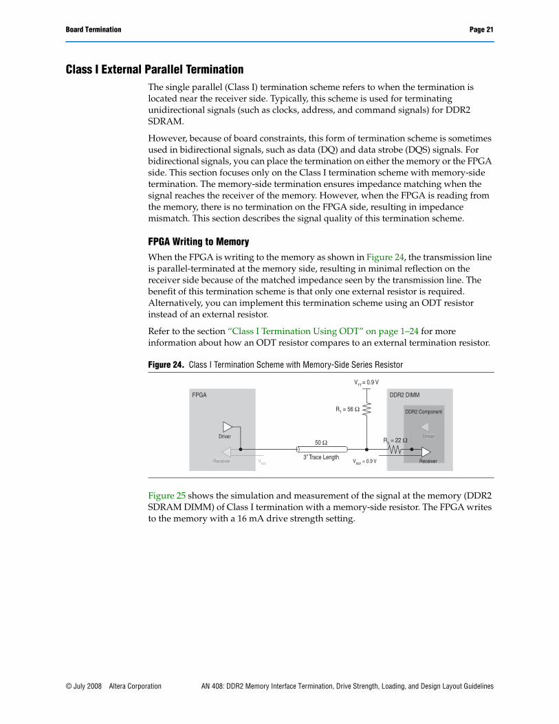
FPGA Writing to MemoryWhen the FPGA is writing to the memory as shown in Figure 24, the transmission line is parallel-terminated at the memory side, resulting in minimal reflection on the receiver side because of the matched impedance seen by the transmission line. The benefit of this termination scheme is that only one external resistor is required. Alternatively, you can implement this termination scheme using an ODT resistor instead of an external resistor.
Refer to the section “Class I Termination Using ODT” on page 1–24 for more information about how an ODT resistor compares to an external termination resistor.
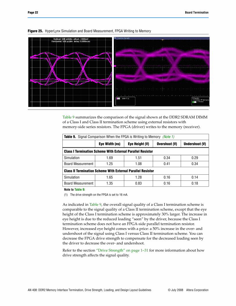
Figure 25 shows the simulation and measurement of the signal at the memory (DDR2 SDRAM DIMM) of Class I termination with a memory-side resistor. The FPGA writes to the memory with a 16 mA drive strength setting.
Figure 24. Class I Termination Scheme with Memory-Side Series Resistor
RT = 56 Ω
VTT = 0.9 V
FPGA DDR2 DIMM
DDR2 Component
RS = 22 Ω
VREF
Driver Driver
Receiver
50 Ω
3” Trace LengthReceiverVREF = 0.9 V
© July 2008 Altera Corporation AN 408: DDR2 Memory Interface Termination, Drive Strength, Loading, and Design Layout Guidelines
Page 22 Board Termination
Table 9 summarizes the comparison of the signal shown at the DDR2 SDRAM DIMM of a Class I and Class II termination scheme using external resistors with memory-side series resistors. The FPGA (driver) writes to the memory (receiver).
As indicated in Table 9, the overall signal quality of a Class I termination scheme is comparable to the signal quality of a Class II termination scheme, except that the eye height of the Class I termination scheme is approximately 30% larger. The increase in eye height is due to the reduced loading “seen” by the driver, because the Class I termination scheme does not have an FPGA-side parallel termination resistor. However, increased eye height comes with a price: a 50% increase in the over- and undershoot of the signal using Class I versus Class II termination scheme. You can decrease the FPGA drive strength to compensate for the decreased loading seen by the driver to decrease the over- and undershoot.
Refer to the section “Drive Strength” on page 1–31 for more information about how drive strength affects the signal quality.
Figure 25. HyperLynx Simulation and Board Measurement, FPGA Writing to Memory
Table 9. Signal Comparison When the FPGA is Writing to Memory (Note 1)
Eye Width (ns) Eye Height (V) Overshoot (V) Undershoot (V)
Class I Termination Scheme With External Parallel Resistor
Simulation 1.69 1.51 0.34 0.29
Board Measurement 1.25 1.08 0.41 0.34
Class II Termination Scheme With External Parallel Resistor
Simulation 1.65 1.28 0.16 0.14
Board Measurement 1.35 0.83 0.16 0.18
Note to Table 9:
(1) The drive strength on the FPGA is set to 16 mA.
AN 408: DDR2 Memory Interface Termination, Drive Strength, Loading, and Design Layout Guidelines © July 2008 Altera Corporation
Board Termination Page 23
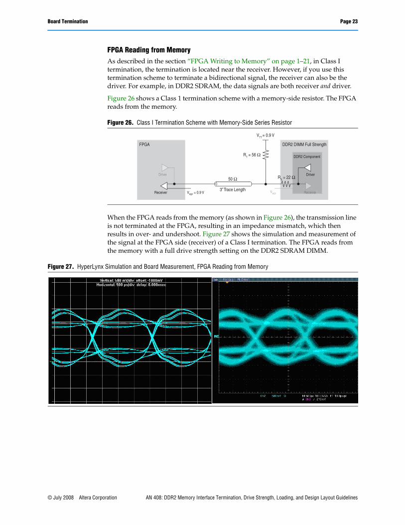
FPGA Reading from MemoryAs described in the section “FPGA Writing to Memory” on page 1–21, in Class I termination, the termination is located near the receiver. However, if you use this termination scheme to terminate a bidirectional signal, the receiver can also be the driver. For example, in DDR2 SDRAM, the data signals are both receiver and driver.
Figure 26 shows a Class 1 termination scheme with a memory-side resistor. The FPGA reads from the memory.
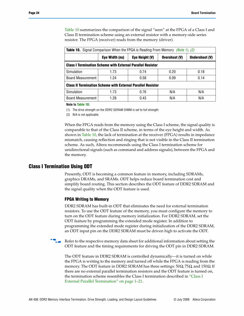
When the FPGA reads from the memory (as shown in Figure 26), the transmission line is not terminated at the FPGA, resulting in an impedance mismatch, which then results in over- and undershoot. Figure 27 shows the simulation and measurement of the signal at the FPGA side (receiver) of a Class I termination. The FPGA reads from the memory with a full drive strength setting on the DDR2 SDRAM DIMM.
Figure 26. Class I Termination Scheme with Memory-Side Series Resistor
RT = 56 Ω
VTT = 0.9 V
FPGA DDR2 DIMM Full Strength
DDR2 Component
RS = 22 Ω
VREF = 0.9 V
Driver Driver
Receiver
50 Ω
3” Trace LengthReceiverReceiverVREF
Figure 27. HyperLynx Simulation and Board Measurement, FPGA Reading from Memory
© July 2008 Altera Corporation AN 408: DDR2 Memory Interface Termination, Drive Strength, Loading, and Design Layout Guidelines
Page 24 Board Termination
Table 10 summarizes the comparison of the signal “seen” at the FPGA of a Class I and Class II termination scheme using an external resistor with a memory-side series resistor. The FPGA (receiver) reads from the memory (driver).
When the FPGA reads from the memory using the Class I scheme, the signal quality is comparable to that of the Class II scheme, in terms of the eye height and width. As shown in Table 10, the lack of termination at the receiver (FPGA) results in impedance mismatch, causing reflection and ringing that is not visible in the Class II termination scheme. As such, Altera recommends using the Class I termination scheme for unidirectional signals (such as command and address signals), between the FPGA and the memory.
Class I Termination Using ODTPresently, ODT is becoming a common feature in memory, including SDRAMs, graphics DRAMs, and SRAMs. ODT helps reduce board termination cost and simplify board routing. This section describes the ODT feature of DDR2 SDRAM and the signal quality when the ODT feature is used.
FPGA Writing to MemoryDDR2 SDRAM has built-in ODT that eliminates the need for external termination resistors. To use the ODT feature of the memory, you must configure the memory to turn on the ODT feature during memory initialization. For DDR2 SDRAM, set the ODT feature by programming the extended mode register. In addition to programming the extended mode register during initialization of the DDR2 SDRAM, an ODT input pin on the DDR2 SDRAM must be driven high to activate the ODT.
f Refer to the respective memory data sheet for additional information about setting the ODT feature and the timing requirements for driving the ODT pin in DDR2 SDRAM.
The ODT feature in DDR2 SDRAM is controlled dynamically—it is turned on while the FPGA is writing to the memory and turned off while the FPGA is reading from the memory. The ODT feature in DDR2 SDRAM has three settings: 50Ω, 75Ω, and 150Ω. If there are no external parallel termination resistors and the ODT feature is turned on, the termination scheme resembles the Class I termination described in “Class I External Parallel Termination” on page 1–21.
Table 10. Signal Comparison When the FPGA is Reading From Memory (Note 1), (2)
Eye Width (ns) Eye Height (V) Overshoot (V) Undershoot (V)
Class I Termination Scheme with External Parallel Resistor
Simulation 1.73 0.74 0.20 0.18
Board Measurement 1.24 0.58 0.09 0.14
Class II Termination Scheme with External Parallel Resistor
Simulation 1.73 0.76 N/A N/A
Board Measurement 1.28 0.43 N/A N/A
Note to Table 10:
(1) The drive strength on the DDR2 SDRAM DIMM is set to full strength.(2) N/A is not applicable.
AN 408: DDR2 Memory Interface Termination, Drive Strength, Loading, and Design Layout Guidelines © July 2008 Altera Corporation
Board Termination Page 25
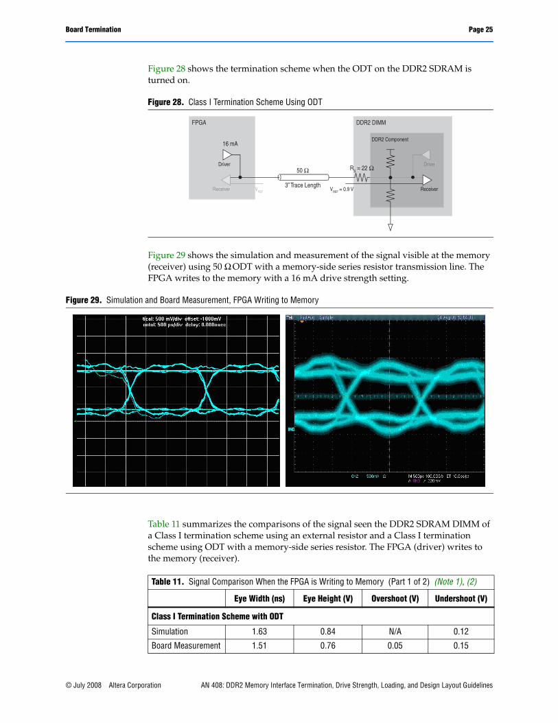
Figure 28 shows the termination scheme when the ODT on the DDR2 SDRAM is turned on.
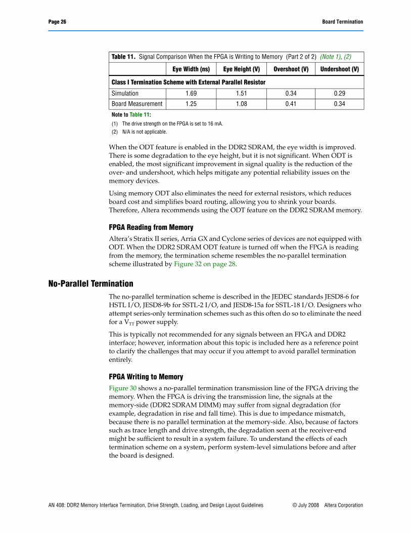
Figure 29 shows the simulation and measurement of the signal visible at the memory (receiver) using 50 Ω ODT with a memory-side series resistor transmission line. The FPGA writes to the memory with a 16 mA drive strength setting.
Table 11 summarizes the comparisons of the signal seen the DDR2 SDRAM DIMM of a Class I termination scheme using an external resistor and a Class I termination scheme using ODT with a memory-side series resistor. The FPGA (driver) writes to the memory (receiver).
Figure 28. Class I Termination Scheme Using ODT
FPGA DDR2 DIMM
DDR2 Component
RS = 22 Ω
VREF = 0.9 V
Driver Driver
Receiver
50 Ω
3” Trace LengthReceiverVVREF
16 mA
Figure 29. Simulation and Board Measurement, FPGA Writing to Memory
Table 11. Signal Comparison When the FPGA is Writing to Memory (Part 1 of 2) (Note 1), (2)
Eye Width (ns) Eye Height (V) Overshoot (V) Undershoot (V)
Class I Termination Scheme with ODT
Simulation 1.63 0.84 N/A 0.12
Board Measurement 1.51 0.76 0.05 0.15
© July 2008 Altera Corporation AN 408: DDR2 Memory Interface Termination, Drive Strength, Loading, and Design Layout Guidelines
Page 26 Board Termination
When the ODT feature is enabled in the DDR2 SDRAM, the eye width is improved. There is some degradation to the eye height, but it is not significant. When ODT is enabled, the most significant improvement in signal quality is the reduction of the over- and undershoot, which helps mitigate any potential reliability issues on the memory devices.
Using memory ODT also eliminates the need for external resistors, which reduces board cost and simplifies board routing, allowing you to shrink your boards. Therefore, Altera recommends using the ODT feature on the DDR2 SDRAM memory.
FPGA Reading from MemoryAltera’s Stratix II series, Arria GX and Cyclone series of devices are not equipped with ODT. When the DDR2 SDRAM ODT feature is turned off when the FPGA is reading from the memory, the termination scheme resembles the no-parallel termination scheme illustrated by Figure 32 on page 28.
No-Parallel TerminationThe no-parallel termination scheme is described in the JEDEC standards JESD8-6 for HSTL I/O, JESD8-9b for SSTL-2 I/O, and JESD8-15a for SSTL-18 I/O. Designers who attempt series-only termination schemes such as this often do so to eliminate the need for a VTT power supply.
This is typically not recommended for any signals between an FPGA and DDR2 interface; however, information about this topic is included here as a reference point to clarify the challenges that may occur if you attempt to avoid parallel termination entirely.
FPGA Writing to MemoryFigure 30 shows a no-parallel termination transmission line of the FPGA driving the memory. When the FPGA is driving the transmission line, the signals at the memory-side (DDR2 SDRAM DIMM) may suffer from signal degradation (for example, degradation in rise and fall time). This is due to impedance mismatch, because there is no parallel termination at the memory-side. Also, because of factors such as trace length and drive strength, the degradation seen at the receiver-end might be sufficient to result in a system failure. To understand the effects of each termination scheme on a system, perform system-level simulations before and after the board is designed.
Class I Termination Scheme with External Parallel Resistor
Simulation 1.69 1.51 0.34 0.29
Board Measurement 1.25 1.08 0.41 0.34
Note to Table 11:
(1) The drive strength on the FPGA is set to 16 mA.(2) N/A is not applicable.
Table 11. Signal Comparison When the FPGA is Writing to Memory (Part 2 of 2) (Note 1), (2)
Eye Width (ns) Eye Height (V) Overshoot (V) Undershoot (V)
AN 408: DDR2 Memory Interface Termination, Drive Strength, Loading, and Design Layout Guidelines © July 2008 Altera Corporation
Board Termination Page 27
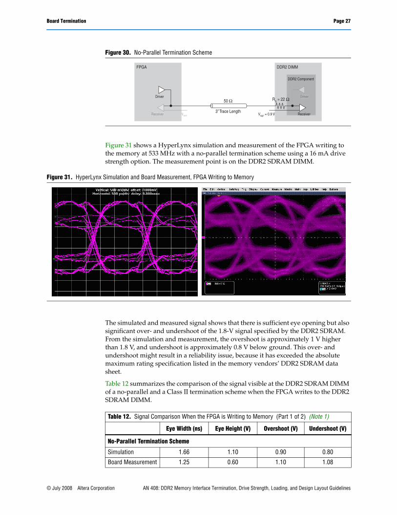
Figure 31 shows a HyperLynx simulation and measurement of the FPGA writing to the memory at 533 MHz with a no-parallel termination scheme using a 16 mA drive strength option. The measurement point is on the DDR2 SDRAM DIMM.
The simulated and measured signal shows that there is sufficient eye opening but also significant over- and undershoot of the 1.8-V signal specified by the DDR2 SDRAM. From the simulation and measurement, the overshoot is approximately 1 V higher than 1.8 V, and undershoot is approximately 0.8 V below ground. This over- and undershoot might result in a reliability issue, because it has exceeded the absolute maximum rating specification listed in the memory vendors’ DDR2 SDRAM data sheet.
Table 12 summarizes the comparison of the signal visible at the DDR2 SDRAM DIMM of a no-parallel and a Class II termination scheme when the FPGA writes to the DDR2 SDRAM DIMM.
Figure 30. No-Parallel Termination Scheme
FPGA DDR2 DIMM
DDR2 Component
RS = 22 Ω
VVREF VREF = 0.9 V
Driver Driver
Receiver
50 Ω
3” Trace LengthReceiver
Figure 31. HyperLynx Simulation and Board Measurement, FPGA Writing to Memory
Table 12. Signal Comparison When the FPGA is Writing to Memory (Part 1 of 2) (Note 1)
Eye Width (ns) Eye Height (V) Overshoot (V) Undershoot (V)
No-Parallel Termination Scheme
Simulation 1.66 1.10 0.90 0.80
Board Measurement 1.25 0.60 1.10 1.08
© July 2008 Altera Corporation AN 408: DDR2 Memory Interface Termination, Drive Strength, Loading, and Design Layout Guidelines
Page 28 Board Termination
Although the appearance of the signal in a no-parallel termination scheme is not clean, when you take the key parameters into consideration, the eye width and height is comparable to that of a Class II termination scheme. The major disadvantage of using a no-parallel termination scheme is the over- and undershoot. There is no termination on the receiver, so there is an impedance mismatch when the signal arrives at the receiver, resulting in ringing and reflection. In addition, the 16-mA drive strength setting on the FPGA also results in overdriving the transmission line, causing the over- and undershoot. By reducing the drive strength setting, the over- and undershoot decreases and improves the signal quality “seen” by the receiver.
For more information about how drive strength affects the signal quality, refer to “Drive Strength” on page 1–31.
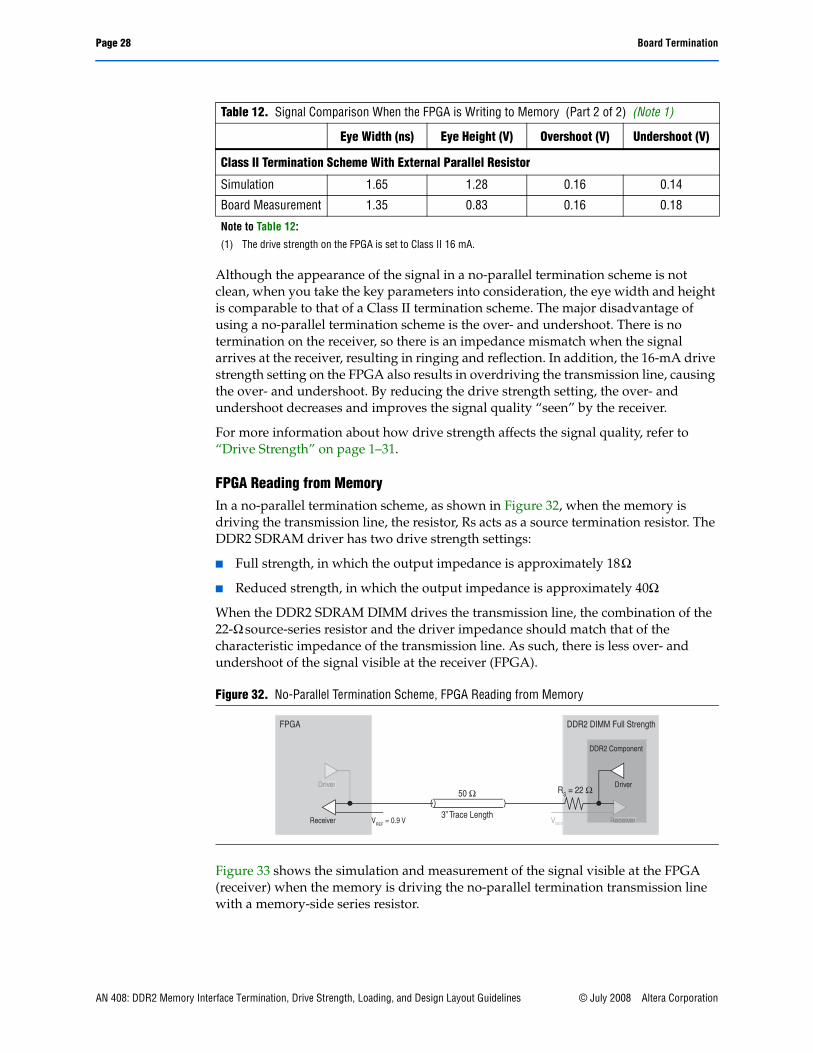
FPGA Reading from MemoryIn a no-parallel termination scheme, as shown in Figure 32, when the memory is driving the transmission line, the resistor, Rs acts as a source termination resistor. The DDR2 SDRAM driver has two drive strength settings:
■ Full strength, in which the output impedance is approximately 18Ω
■ Reduced strength, in which the output impedance is approximately 40Ω
When the DDR2 SDRAM DIMM drives the transmission line, the combination of the 22-Ω source-series resistor and the driver impedance should match that of the characteristic impedance of the transmission line. As such, there is less over- and undershoot of the signal visible at the receiver (FPGA).
Figure 33 shows the simulation and measurement of the signal visible at the FPGA (receiver) when the memory is driving the no-parallel termination transmission line with a memory-side series resistor.
Class II Termination Scheme With External Parallel Resistor
Simulation 1.65 1.28 0.16 0.14
Board Measurement 1.35 0.83 0.16 0.18
Note to Table 12:
(1) The drive strength on the FPGA is set to Class II 16 mA.
Figure 32. No-Parallel Termination Scheme, FPGA Reading from Memory
Table 12. Signal Comparison When the FPGA is Writing to Memory (Part 2 of 2) (Note 1)
Eye Width (ns) Eye Height (V) Overshoot (V) Undershoot (V)
FPGA DDR2 DIMM Full Strength
DDR2 Component
RS = 22 Ω
VREFFVREF = 0.9 V
Driver Driver
Receiver
50 Ω
3” Trace LengthReceiverReceiver
AN 408: DDR2 Memory Interface Termination, Drive Strength, Loading, and Design Layout Guidelines © July 2008 Altera Corporation
Board Termination Page 29
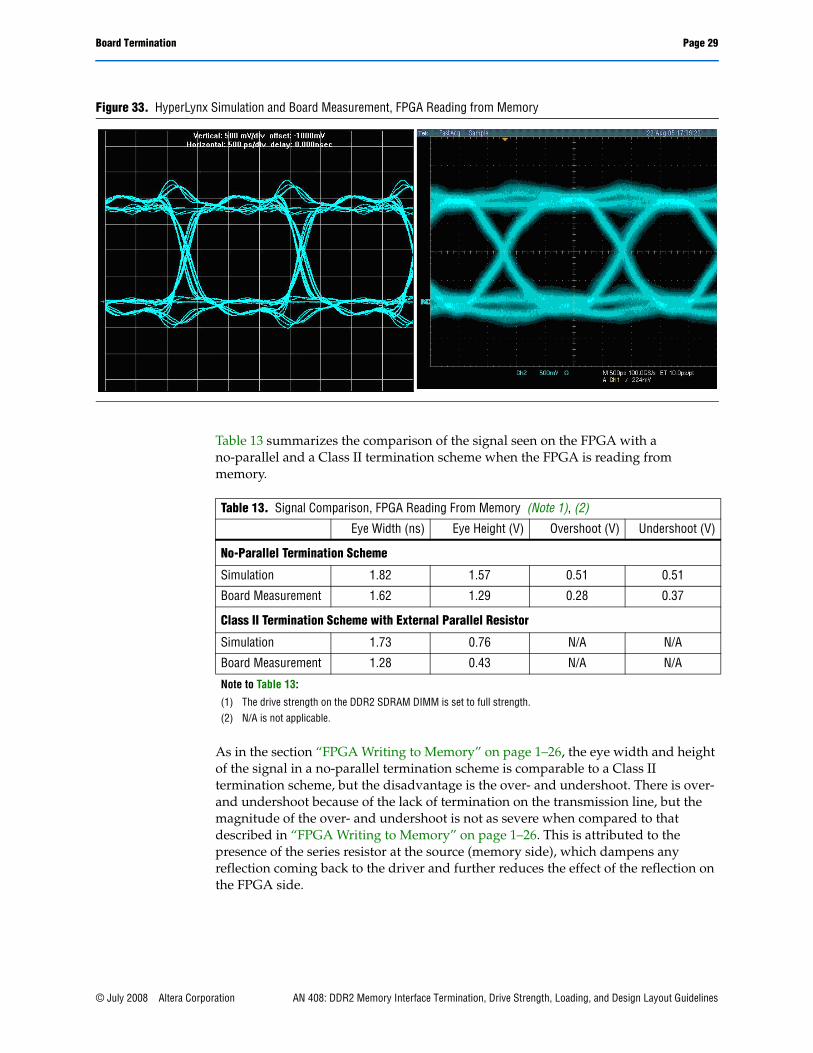
Table 13 summarizes the comparison of the signal seen on the FPGA with a no-parallel and a Class II termination scheme when the FPGA is reading from memory.
As in the section “FPGA Writing to Memory” on page 1–26, the eye width and height of the signal in a no-parallel termination scheme is comparable to a Class II termination scheme, but the disadvantage is the over- and undershoot. There is over- and undershoot because of the lack of termination on the transmission line, but the magnitude of the over- and undershoot is not as severe when compared to that described in “FPGA Writing to Memory” on page 1–26. This is attributed to the presence of the series resistor at the source (memory side), which dampens any reflection coming back to the driver and further reduces the effect of the reflection on the FPGA side.
Figure 33. HyperLynx Simulation and Board Measurement, FPGA Reading from Memory
Table 13. Signal Comparison, FPGA Reading From Memory (Note 1), (2)
Eye Width (ns) Eye Height (V) Overshoot (V) Undershoot (V)
No-Parallel Termination Scheme
Simulation 1.82 1.57 0.51 0.51
Board Measurement 1.62 1.29 0.28 0.37
Class II Termination Scheme with External Parallel Resistor
Simulation 1.73 0.76 N/A N/A
Board Measurement 1.28 0.43 N/A N/A
Note to Table 13:
(1) The drive strength on the DDR2 SDRAM DIMM is set to full strength.(2) N/A is not applicable.
© July 2008 Altera Corporation AN 408: DDR2 Memory Interface Termination, Drive Strength, Loading, and Design Layout Guidelines
Page 30 Board Termination
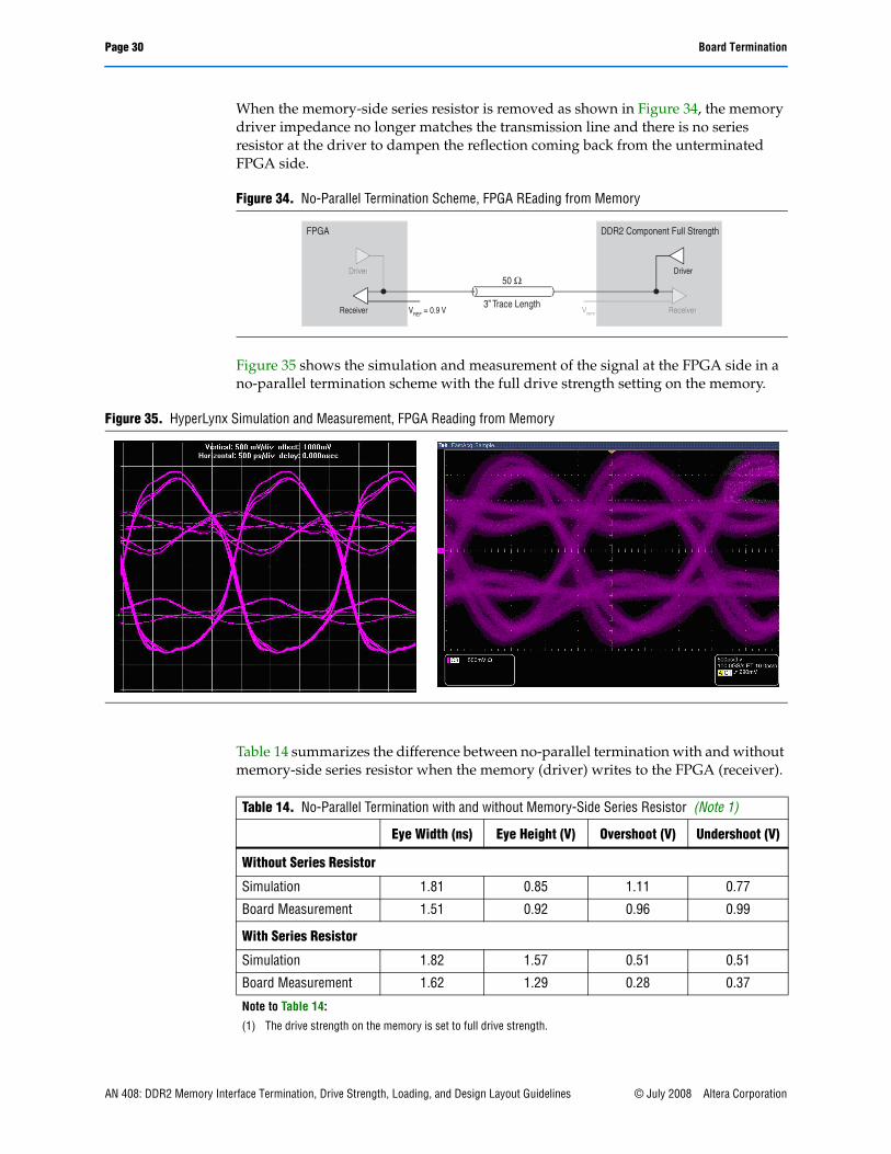
When the memory-side series resistor is removed as shown in Figure 34, the memory driver impedance no longer matches the transmission line and there is no series resistor at the driver to dampen the reflection coming back from the unterminated FPGA side.
Figure 35 shows the simulation and measurement of the signal at the FPGA side in a no-parallel termination scheme with the full drive strength setting on the memory.
Table 14 summarizes the difference between no-parallel termination with and without memory-side series resistor when the memory (driver) writes to the FPGA (receiver).
Figure 34. No-Parallel Termination Scheme, FPGA REading from Memory
FPGA DDR2 Component Full Strength
VREFVREF = 0.9 V
Driver Driver
Receiver
50 Ω
3” Trace LengthReceiver
Figure 35. HyperLynx Simulation and Measurement, FPGA Reading from Memory
Table 14. No-Parallel Termination with and without Memory-Side Series Resistor (Note 1)
Eye Width (ns) Eye Height (V) Overshoot (V) Undershoot (V)
Without Series Resistor
Simulation 1.81 0.85 1.11 0.77
Board Measurement 1.51 0.92 0.96 0.99
With Series Resistor
Simulation 1.82 1.57 0.51 0.51
Board Measurement 1.62 1.29 0.28 0.37
Note to Table 14:
(1) The drive strength on the memory is set to full drive strength.
AN 408: DDR2 Memory Interface Termination, Drive Strength, Loading, and Design Layout Guidelines © July 2008 Altera Corporation
Drive Strength Page 31
Table 14 highlights the effect of the series resistor on the memory side with the dramatic increase in over- and undershoot and the decrease in the eye height. This result is similar to that described in “FPGA Writing to Memory” on page 1–26. In that simulation, there is a series resistor but it is located at the receiver side (memory-side), so it does not have the desired effect of reducing the drive strength of the driver and suppressing the reflection coming back from the unterminated receiver-end. As such, in a system without receiver-side termination, the series resistor on the driver helps reduce the drive strength of the driver and dampen the reflection coming back from the unterminated receiver-end.
SummaryThis section compared the various types of termination schemes and studied the benefits and disadvantages of each scheme.
For bidirectional signals, such as the DQ and DQS signals of DDR2 SDRAM, dynamic OCT should be regarded as the ideal termination method when the feature is available; otherwise, a Class II termination scheme with fly-by topology should be regarded as the ideal termination method.
For unidirectional signals, such as the command and address signals of DDR and DDR2 SDRAM, a memory-side Class I termination scheme with fly-by topology provides the best results.
If board real estate and cost is prohibitive to placing on-board termination resistors, you can use the ODT feature on the DDR2 SDRAM memory for the memory-side Class II termination when the controller drives the transmission line. If a Stratix III series device is used, dynamic OCT can be utilized to achieve a termination solution comparable to a fully discrete terminated system.
Drive StrengthAltera’s FPGA products offer numerous drive strength settings, allowing you to optimize your board designs to achieve the best signal quality. This section focuses on the most commonly used drive strength settings of 8 mA and 16 mA, as recommended by JEDEC for Class I and Class II termination schemes.
1 You are not restricted to using only these drive strength settings for your board designs. You should perform simulations using I/O models available from Altera and memory vendors to ensure that you use the proper drive strength setting to achieve optimum signal integrity.
How Strong is Strong Enough?Figure 20 on page 18 shows a signal probed at the DDR2 SDRAM DIMM (receiver) of a far-end series-terminated transmission line when the FPGA writes to the DDR2 SDRAM DIMM using a drive strength setting of 16 mA. The resulting signal quality on the receiver shows excessive over- and undershoot. To reduce the over- and undershoot, you can reduce the drive strength setting on the FPGA from 16 mA to 8 mA. Figure 36 shows the simulation and measurement of the FPGA with a drive strength setting of 8 mA driving a no-parallel termination transmission line.
© July 2008 Altera Corporation AN 408: DDR2 Memory Interface Termination, Drive Strength, Loading, and Design Layout Guidelines
Page 32 Drive Strength
Table 15 compares the signals at the DDR2 SDRAM DIMM with no-parallel termination and memory-side series resistors when the FPGA is writing to the memory with 8-mA and 16-mA drive strength settings.
With a lower strength drive setting, the overall signal quality is improved. The eye width is reduced, but the eye height is significantly larger with a lower drive strength and the over- and undershoot is reduced dramatically.
To improve the signal quality further, you should use 50-Ω on-chip series termination in place of an 8mA drive strength and 25-Ω on-chip series termination in place of a 16 mA drive strength. Refer to “On-Chip Termination (Non-Dynamic)” on page 1–14 for simulation and board measurements.
SummaryThis section compared the effects of drive strength on the signal quality seen at the receiver. As shown, the drive strength setting is highly dependent on the termination scheme, so it is critical that you perform pre- and post-layout board-level simulations to determine the proper drive strength settings. However, it has been shown in page 14 through page 16 that 50-Ω OCT and 25-Ω OCT drive strength settings for
Figure 36. HyperLynx Simulation and Measurement, FPGA Writing to Memory
Table 15. Simulation and Board Measurement Results for 8 mA and 16 mA Drive Strength Settings
Eye Width (ns) Eye Height (V) Overshoot (V) Undershoot (V)
8-mA Drive Strength Setting
Simulation 1.48 1.71 0.24 0.35
Board Measurement 1.10 1.24 0.24 0.50
16-mA Drive Strength Setting
Simulation 1.66 1.10 0.90 0.80
Board Measurements 1.25 0.60 1.10 1.08
AN 408: DDR2 Memory Interface Termination, Drive Strength, Loading, and Design Layout Guidelines © July 2008 Altera Corporation
System Loading Page 33
Class I and Class II, respectively, provide the optimum signal quality because the output driver matches the impedance “seen” by the driver. In addition, using the OCT feature in Altera’s FPGA devices eliminates the need for external series resistors and simplifies board design. Finally, using the FPGA’s OCT with the SDRAM ODT feature results in the best signal quality without any over- or undershoot.
System LoadingYou can use memory in a variety of forms, such as individual components or multiple DIMMs, resulting in different loading seen by the FPGA. This section describes the effect on signal quality when interfacing memories in component, dual rank, and dual DIMMs format.
Component Versus DIMMWhen using discrete DDR2 SDRAM components, the additional loading from the DDR2 SDRAM DIMM connector is eliminated and the memory-side series resistor on the DDR2 SDRAM DIMM is no longer there. You must decide if the memory-side series resistor near the DDR2 SDRAM is required.
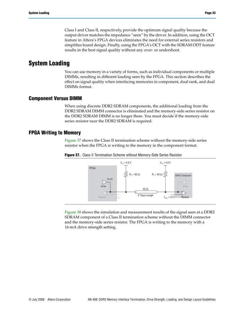
FPGA Writing to MemoryFigure 37 shows the Class II termination scheme without the memory-side series resistor when the FPGA is writing to the memory in the component format.
Figure 38 shows the simulation and measurement results of the signal seen at a DDR2 SDRAM component of a Class II termination scheme without the DIMM connector and the memory-side series resistor. The FPGA is writing to the memory with a 16-mA drive strength setting.
Figure 37. Class II Termination Scheme without Memory-Side Series Resistor
RT = 56 Ω
VTT = 0.9 V
RT = 56 Ω
VTT = 0.9 V
FPGA
DDR2 Component
VVREF VREF = 0.9 V
Driver Driver
Receiver
50 Ω
3” Trace LengthReceiver
16 mA
© July 2008 Altera Corporation AN 408: DDR2 Memory Interface Termination, Drive Strength, Loading, and Design Layout Guidelines
Page 34 System Loading
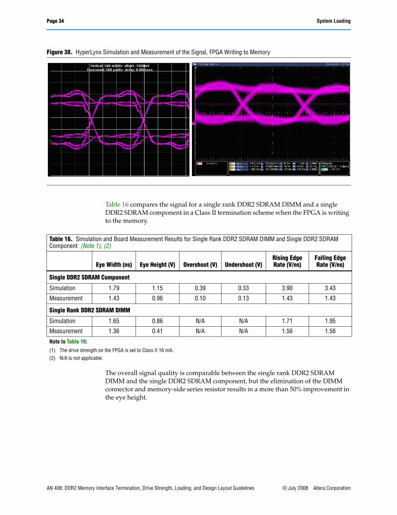
Table 16 compares the signal for a single rank DDR2 SDRAM DIMM and a single DDR2 SDRAM component in a Class II termination scheme when the FPGA is writing to the memory.
The overall signal quality is comparable between the single rank DDR2 SDRAM DIMM and the single DDR2 SDRAM component, but the elimination of the DIMM connector and memory-side series resistor results in a more than 50% improvement in the eye height.
Figure 38. HyperLynx Simulation and Measurement of the Signal, FPGA Writing to Memory
Table 16. Simulation and Board Measurement Results for Single Rank DDR2 SDRAM DIMM and Single DDR2 SDRAM Component (Note 1), (2)
Eye Width (ns) Eye Height (V) Overshoot (V) Undershoot (V)Rising Edge Rate (V/ns)
Falling Edge Rate (V/ns)
Single DDR2 SDRAM Component
Simulation 1.79 1.15 0.39 0.33 3.90 3.43
Measurement 1.43 0.96 0.10 0.13 1.43 1.43
Single Rank DDR2 SDRAM DIMM
Simulation 1.65 0.86 N/A N/A 1.71 1.95
Measurement 1.36 0.41 N/A N/A 1.56 1.56
Note to Table 16:
(1) The drive strength on the FPGA is set to Class II 16 mA.(2) N/A is not applicable.
AN 408: DDR2 Memory Interface Termination, Drive Strength, Loading, and Design Layout Guidelines © July 2008 Altera Corporation
System Loading Page 35
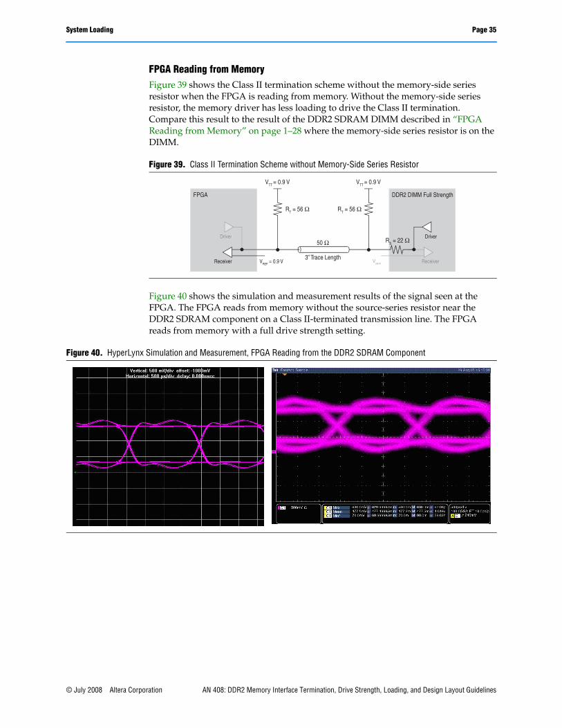
FPGA Reading from MemoryFigure 39 shows the Class II termination scheme without the memory-side series resistor when the FPGA is reading from memory. Without the memory-side series resistor, the memory driver has less loading to drive the Class II termination. Compare this result to the result of the DDR2 SDRAM DIMM described in “FPGA Reading from Memory” on page 1–28 where the memory-side series resistor is on the DIMM.
Figure 40 shows the simulation and measurement results of the signal seen at the FPGA. The FPGA reads from memory without the source-series resistor near the DDR2 SDRAM component on a Class II-terminated transmission line. The FPGA reads from memory with a full drive strength setting.
Figure 39. Class II Termination Scheme without Memory-Side Series Resistor
RT = 56 Ω
VTT = 0.9 V
RT = 56 Ω
VTT = 0.9 V
FPGA DDR2 DIMM Full Strength
RS = 22 Ω
VREFVREF = 0.9 V
Driver Driver
Receiver
50 Ω
3” Trace LengthReceiver
Figure 40. HyperLynx Simulation and Measurement, FPGA Reading from the DDR2 SDRAM Component
© July 2008 Altera Corporation AN 408: DDR2 Memory Interface Termination, Drive Strength, Loading, and Design Layout Guidelines
Page 36 System Loading
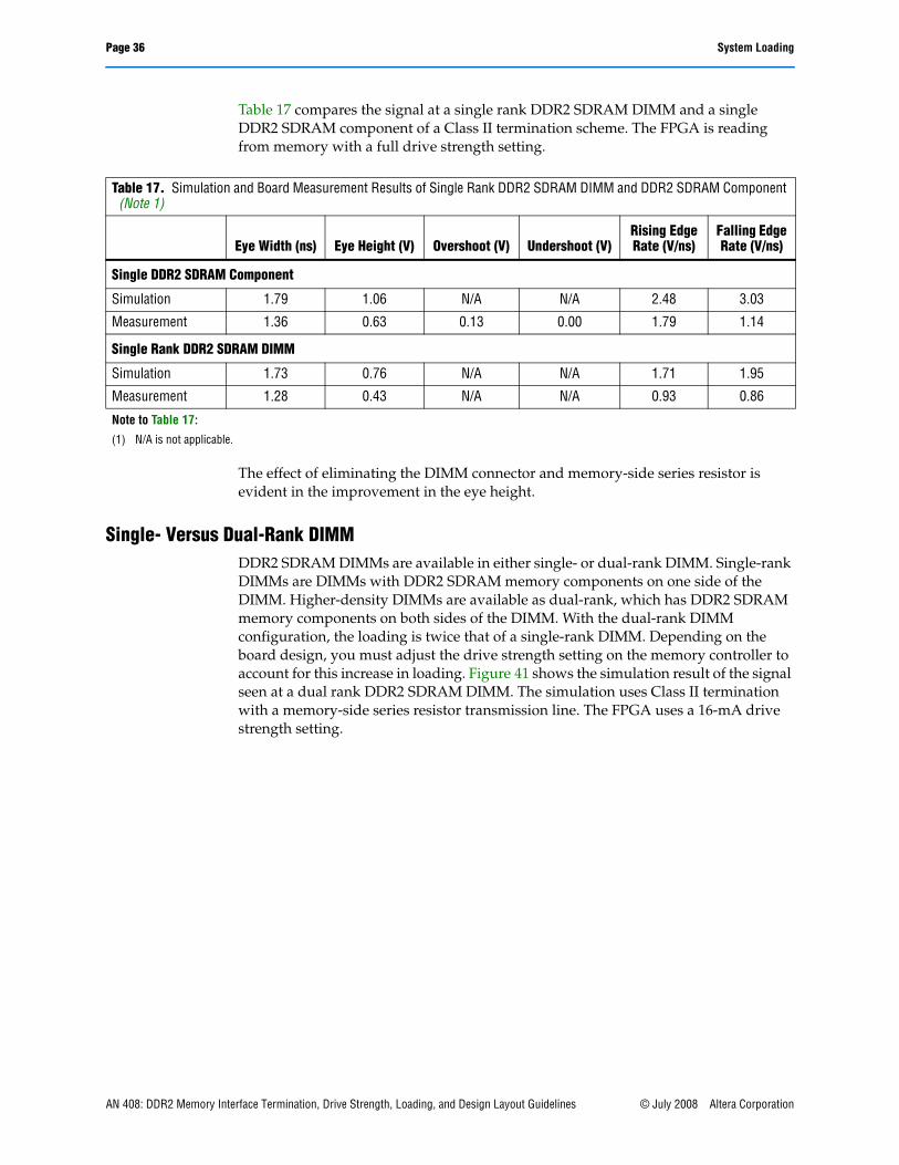
Table 17 compares the signal at a single rank DDR2 SDRAM DIMM and a single DDR2 SDRAM component of a Class II termination scheme. The FPGA is reading from memory with a full drive strength setting.
The effect of eliminating the DIMM connector and memory-side series resistor is evident in the improvement in the eye height.
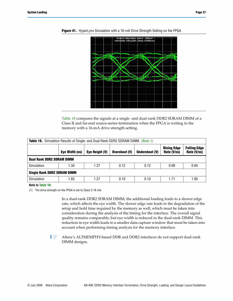
Single- Versus Dual-Rank DIMMDDR2 SDRAM DIMMs are available in either single- or dual-rank DIMM. Single-rank DIMMs are DIMMs with DDR2 SDRAM memory components on one side of the DIMM. Higher-density DIMMs are available as dual-rank, which has DDR2 SDRAM memory components on both sides of the DIMM. With the dual-rank DIMM configuration, the loading is twice that of a single-rank DIMM. Depending on the board design, you must adjust the drive strength setting on the memory controller to account for this increase in loading. Figure 41 shows the simulation result of the signal seen at a dual rank DDR2 SDRAM DIMM. The simulation uses Class II termination with a memory-side series resistor transmission line. The FPGA uses a 16-mA drive strength setting.
Table 17. Simulation and Board Measurement Results of Single Rank DDR2 SDRAM DIMM and DDR2 SDRAM Component (Note 1)
Eye Width (ns) Eye Height (V) Overshoot (V) Undershoot (V)Rising Edge Rate (V/ns)
Falling Edge Rate (V/ns)
Single DDR2 SDRAM Component
Simulation 1.79 1.06 N/A N/A 2.48 3.03
Measurement 1.36 0.63 0.13 0.00 1.79 1.14
Single Rank DDR2 SDRAM DIMM
Simulation 1.73 0.76 N/A N/A 1.71 1.95
Measurement 1.28 0.43 N/A N/A 0.93 0.86
Note to Table 17: (1) N/A is not applicable.
AN 408: DDR2 Memory Interface Termination, Drive Strength, Loading, and Design Layout Guidelines © July 2008 Altera Corporation
System Loading Page 37
Table 18 compares the signals at a single- and dual-rank DDR2 SDRAM DIMM of a Class II and far-end source-series termination when the FPGA is writing to the memory with a 16-mA drive strength setting.
In a dual-rank DDR2 SDRAM DIMM, the additional loading leads to a slower edge rate, which affects the eye width. The slower edge rate leads to the degradation of the setup and hold time required by the memory as well, which must be taken into consideration during the analysis of the timing for the interface. The overall signal quality remains comparable, but eye width is reduced in the dual-rank DIMM. This reduction in eye width leads to a smaller data capture window that must be taken into account when performing timing analysis for the memory interface.
1 Altera’s ALTMEMPHY-based DDR and DDR2 interfaces do not support dual-rank DIMM designs.
Figure 41. HyperLynx Simulation with a 16-mA Drive Strength Setting on the FPGA
Table 18. Simulation Results of Single- and Dual-Rank DDR2 SDRAM DIMM (Note 1)
Eye Width (ns) Eye Height (V) Overshoot (V) Undershoot (V)Rising Edge Rate (V/ns)
Falling Edge Rate (V/ns)
Dual Rank DDR2 SDRAM DIMM
Simulation 1.34 1.27 0.12 0.12 0.99 0.94
Single Rank DDR2 SDRAM DIMM
Simulation 1.65 1.27 0.10 0.10 1.71 1.95
Note to Table 18:
(1) The drive strength on the FPGA is set to Class II 16 mA.
© July 2008 Altera Corporation AN 408: DDR2 Memory Interface Termination, Drive Strength, Loading, and Design Layout Guidelines
Page 38 DDR2 Design Layout Guidelines
Single DIMM Versus Multiple DIMMsSome applications, such as packet buffering, require deeper memory, making a single DIMM interface insufficient. If you use a multiple DIMM configuration to increase memory depth, the memory controller is required to interface with multiple data strobes and the data lines instead of the point-to-point interface in a single DIMM configuration. This results in heavier loading on the interface, which can potentially impact the overall performance of the memory interface.
1 Altera’s ALTMEMPHY-based DDR and DDR2 interfaces do not support multiple DIMM designs.
f For detailed information about a multiple DIMM DDR2 SDRAM memory interface, refer to AN 444: Dual DIMM DDR2 SDRAM Memory Interface Design Guidelines.
SummaryThis section compared the effects of various loading styles on the system. With larger loading, the eye width is reduced, shrinking the data capture window, which must be taken into account when performing the timing analysis for the memory interface.
DDR2 Design Layout GuidelinesTable 19 summarizes DDR2 layout guidelines.
Table 19. DDR2 Layout Guidelines (Part 1 of 3) (Note 1)
Parameter Guidelines
DIMMs If you consider a normal DDR2 un-buffered, un-registered DIMM, then essentially you are planning to perform the DIMM routing directly on your PCB. Therefore, each address and control pin routes from the FPGA (single pin) to all memory devices must be on the same side of the FPGA.
Impedance ■ All signal planes must be 50-60-Ω, single-ended, ±10%
■ All signal planes must be 100Ω, differential ±10%
■ All unused via pads must be removed, because they cause unwanted capacitance
Decoupling Parameter ■ Use 0.1μF in 0402 size to minimize inductance
■ Make VTT voltage decoupling close to pull-up resistors
■ Connect decoupling caps between VTT and ground
■ Use a 0.1μF cap for every other VTT pin and 0.01μF cap for every VDD and VDDQ pin
Power ■ GND, 2.5 V/1.8 V must be routed as planes
■ VCCIO for memories must be routed in a single split plane with at least a 20-mil (0.020 inches, or 0.508 mm) gap of separation
■ VTT must be routed as islands or 250-mil (6.35-mm) power traces
■ Oscillators and PLL power must be routed as islands or 100-mil (2.54-mm) power traces
AN 408: DDR2 Memory Interface Termination, Drive Strength, Loading, and Design Layout Guidelines © July 2008 Altera Corporation
DDR2 Design Layout Guidelines Page 39
General Routing ■ Use 45° angles (not 90° corners)
■ Avoid T-Junctions for critical nets or clocks
■ Avoid T-junctions greater than 250 mils (6.35 mm)
■ Disallow signals across split planes
■ Restrict routing other signals close to system reset signals
■ Avoid routing memory signals closer than 0.025 inch (0.635 mm) to PCI or system clocks
■ All data, address, and command signals must have matched length traces ±0.250 inches (6.35 mm)
■ All signals within a given Byte Lane Group should be matched length with maximum deviation of ±0.050 inches (1.27 mm)
Clock Routing ■ Clocks should be routed on inner layers with outer-layer run lengths held to under 500 mils (12.7 mm)
■ These signals should maintain a10-mil (0.254 mm) spacing from other nets
■ Clocks should maintain a length-matching between clock pairs of ±30 mils (0.762 mm)
■ Differential clocks should maintain a length-matching between P and N signals of ±15 mils (0.381 mm), routed in parallel
■ Space between different pairs should be at least three times the space between the differential pairs and must be routed differentially (5-mil trace, 10-15 mil space on centers) and equal to or up to 100 mils (2.54 mm) longer than signals in the Address/Command Group
■ 4.5 inches maximum length
Address and Command Routing
■ Un-buffered address and command lines are more susceptible to cross-talk and are generally noisier than buffered address or command lines. Therefore, un-buffered address and command signals should be routed on a different layer than data signals (DQ) and data mask signals (DM) and with greater spacing.
■ Do not route differential clock (CK) and clock enable (CKE) signals close to address signals.
Table 19. DDR2 Layout Guidelines (Part 2 of 3) (Note 1)
Parameter Guidelines
© July 2008 Altera Corporation AN 408: DDR2 Memory Interface Termination, Drive Strength, Loading, and Design Layout Guidelines
Page 40 DDR2 Design Layout Guidelines
f For more information about how the memory manufacturers route these address and control signals on their DIMMs, refer to the Cadence PCB browser from the Cadence website, at www.cadence.com. The various JEDEC example DIMM layouts are available from the JEDEC website, at www.jedec.org.
External Memory Routing Rules
■ Keep the distance from the pin on the DDR2 DIMM or device to the termination resistor pack (VTT) to less than 500 mils for DQS[x] Data Groups.
■ Keep the distance from the pin on the DDR2 DIMM or device to the termination resistor pack (VTT) to less than 1000 mils for the ADR_CMD_CTL Address Group.
■ Parallelism rules for the DQS[x] Data Groups are as follows:
4 mils for parallel runs < 0.1 inch (approximately 1X spacing relative to plane distance)
5 mils for parallel runs < 0.5 inch (approximately 1X spacing relative to plane distance)
10 mils for parallel runs between 0.5 and 1.0 inches (approximately 2X spacing relative to plane distance)
15 mils for parallel runs between 1.0 and 6.0 inch (approximately 3X spacing relative to plane distance)
■ Parallelism rules for the ADR_CMD_CTL group and CLOCKS group are as follows:
4 mils for parallel runs < 0.1 inch (approximately 1X spacing relative to plane distance)
10 mils for parallel runs < 0.5 inch (approximately 2X spacing relative to plane distance)
15 mils for parallel runs between 0.5 and 1.0 inches (approximately 3X spacing relative to plane distance)
20 mils for parallel runs between 1.0 and 6.0 inches (approximately 4X spacing relative to plane distance)
■ All signals are to maintain a 20-mil separation from other, non-related nets.
■ All signals must have a total length of < 6 inches.
Termination Rules ■ When pull-ups are used, fly-by termination configuration is recommended. Fly-by helps reduce stub reflection issues.
■ Pull-ups should be within 0.5 to no more than 1 inch.
■ Pull up is typically 56 Ω.
■ If using resistor networks:
Do not share R-pack series resistors between address/command and data lines (DQ, DQS, and DM) to eliminate crosstalk within pack.
Series and pull up tolerances are 1–2%.
Series resistors are typically 10 to 20Ω.
Address/Control series resistor typically at the FPGA end of the link.
Data/Strobe/Mask series resistor typically at the memory end of the link (or just before the first DIMM).
■ If termination resistor packs are used:
The distance to your memory device should be less than 750 mils.
The distance from your Altera’s FPGA device should be less than 1250 mils.
Notes to Table 19:
(1) For point-to-point and DIMM interface designs, refer to the Micron website, www.micron.com.
Table 19. DDR2 Layout Guidelines (Part 3 of 3) (Note 1)
Parameter Guidelines
AN 408: DDR2 Memory Interface Termination, Drive Strength, Loading, and Design Layout Guidelines © July 2008 Altera Corporation
Conclusion Page 41
ConclusionThis application note provides Altera’s recommendations about the termination schemes to be used when interfacing Altera FPGA devices with DDR2 SDRAM devices. However, it is very important that you simulate your own design to find the best-suited termination scheme for your design.
This application note also provides data comparisons from simulation and experimental bench results so you can draw your own conclusions for optimum design guidelines to achieve the best signal quality.
For termination schemes, Altera recommends that receiver-side parallel termination be used for best signal quality. Therefore, for a bidirectional signal, such as data (DQ) or data strobe (DQS), the recommended termination scheme is Class II termination. You can implement Class II termination by using external parallel resistors at the FPGA and memory side, ODT and OCT at the memory and FPGA side, or a combination of the DDR2 SDRAM ODT and an external parallel resistor at the FPGA side. For a unidirectional signal, such as command or address, the recommended termination scheme is Class I termination, in which the termination is located at the memory side. (If you use on-chip termination, refer to Table 2 on page 8.)
Choosing the drive strength setting on the FPGA depends on the termination scheme—Class I or Class II—but the simulation results show that you should set the drive strength to match the loading the output driver “sees”. For Class II termination, Altera recommends using 25-Ω OCT drive strength settings. They offer the best results because the impedance of the output driver impedance matches the impedance the output driver sees. For a Class I termination scheme, Altera recommends the 50-Ω OCT drive strength setting.
Moreover, this application note described the effects that different memory loading styles (such as component versus DIMM) have on signal quality. From the results shown in “Single- Versus Dual-Rank DIMM” on page 1–36, the higher loading decreases the edge rates of the signal, thus reducing the eye width visible at the receiver. You can increase the edge rates by using a higher drive strength setting on the FPGA, but the output driver impedance decreases because the higher drive strength setting causes impedance mismatch.
Finally, this application note provided DDR2 layout guidelines. Although the recommendations in this application note are based on the simulations and experimental results of the Stratix III Host Development Kit Board and Stratix II Memory Board 2, you can apply the same general principles when determining the best termination scheme, drive strength setting, and loading style to any board designs. Even armed with this knowledge, it is still critical that you perform simulations, either using IBIS or HSPICE models, to determine the quality of signal integrity on your designs.
© July 2008 Altera Corporation AN 408: DDR2 Memory Interface Termination, Drive Strength, Loading, and Design Layout Guidelines
Page 42 Referenced Documents
Referenced DocumentsThe following documents and websites have been referenced in this application note:
■ AN 444: Dual DIMM DDR2 SDRAM Memory Interface Design Guidelines
■ Cadence website, www.cadence.com
■ JEDEC website, www.jedec.org
■ PC4300 DDR2 SDRAM Unbuffered DIMM Design Specification
■ PC5300/6400 DDR2 SDRAM Unbuffered DIMM Design Specification
■ Stratix III Device I/O Features chapter in the Stratix III Device Handbook
AN 408: DDR2 Memory Interface Termination, Drive Strength, Loading, and Design Layout Guidelines © July 2008 Altera Corporation
Bibliography Page 43
Bibliography“High-Speed Digital Design—A Handbook of Black Magic,” Howard Johnson and Martin Graham, Prentice Hall, 1993.
“Circuits Interconnects, and Packaging for VLSI,“ H.B. Bakoglu, Addison Wesley, 1990.
“Signal Integrity—Simplified,“ Eric Bogatin, Prentice Hall Modern Semiconductor Design Series, 2004.
“Handbook of Digital Techniques for High-Speed Design,“ Tom Granberg, Prentice Hall Modern Semiconductor Design Series, 2004.
“DDR2 Design Guide for Two-DIMM Systems,“ Micron Technical Note, TN-47-01, 2004.
“Termination Placement in PCB Design: How Much Does it Matter?”, Doug Brooks, UltraCAD Design Inc.
“Stratix II Memory Board 2 Rev A User Guide 1.0,“ Altera’s High-Speed/End Applications Team, 2004.
“Stratix II Memory Board 2 Layout Guidelines Rev 0.4,“ Altera’s High-Speed/End Applications Team, 2004.
“Stratix to DDR-I Memory Devices Interface Analysis,“ Altera’s High-Speed/End Applications Team, 2004.
“Multiconductor Transmission Line Analysis for Board-Level Digital Design,“ Emmanuel A. Maitre, Master Thesis, Santa Clara University, 1994.
JEDEC Standard Publication JESD79C, DDR SDRAM Specification, JEDEC Solid State Technology Association.
JEDEC Standard Publication JESD79-2, DDR2 SDRAM Specification, JEDEC Solid State Technology Association.
JEDEC Standard Publication JESD8-9B, Stub Series Termination Logic for 2.5 V (SSTL-2), JEDEC Solid State Technology Association.
JEDEC Standard Publication JESD8-15A, Stub Series Termination Logic for 1.8 V (SSTL-18), JEDEC Solid State Technology Association.
PC4300 DDR2 SDRAM Unbuffered DIMM Design Specification, Revision 0.5, Oct 30, 2003.
© July 2008 Altera Corporation AN 408: DDR2 Memory Interface Termination, Drive Strength, Loading, and Design Layout Guidelines
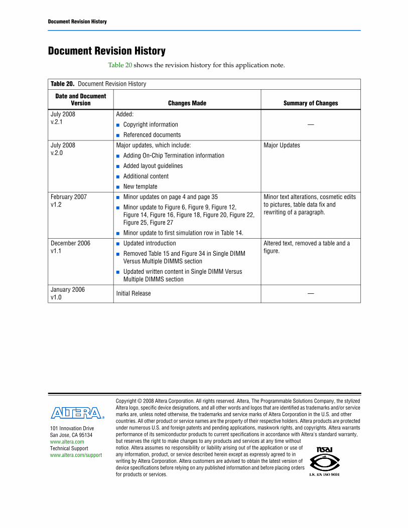
Document Revision History
101 Innovation DriveSan Jose, CA 95134www.altera.comTechnical Supportwww.altera.com/support
Copyright © 2008 Altera Corporation. All rights reserved. Altera, The Programmable Solutions Company, the stylized Altera logo, specific device designations, and all other words and logos that are identified as trademarks and/or service marks are, unless noted otherwise, the trademarks and service marks of Altera Corporation in the U.S. and other countries. All other product or service names are the property of their respective holders. Altera products are protected under numerous U.S. and foreign patents and pending applications, maskwork rights, and copyrights. Altera warrants performance of its semiconductor products to current specifications in accordance with Altera's standard warranty, but reserves the right to make changes to any products and services at any time without notice. Altera assumes no responsibility or liability arising out of the application or use of any information, product, or service described herein except as expressly agreed to in writing by Altera Corporation. Altera customers are advised to obtain the latest version of device specifications before relying on any published information and before placing orders for products or services.
Document Revision History Table 20 shows the revision history for this application note.
Table 20. Document Revision History
Date and Document Version Changes Made Summary of Changes
July 2008v.2.1
Added:
■ Copyright information
■ Referenced documents
—
July 2008 v.2.0
Major updates, which include:
■ Adding On-Chip Termination information
■ Added layout guidelines
■ Additional content
■ New template
Major Updates
February 2007 v1.2
■ Minor updates on page 4 and page 35
■ Minor update to Figure 6, Figure 9, Figure 12, Figure 14, Figure 16, Figure 18, Figure 20, Figure 22, Figure 25, Figure 27
■ Minor update to first simulation row in Table 14.
Minor text alterations, cosmetic edits to pictures, table data fix and rewriting of a paragraph.
December 2006 v1.1
■ Updated introduction
■ Removed Table 15 and Figure 34 in Single DIMM Versus Multiple DIMMS section
■ Updated written content in Single DIMM Versus Multiple DIMMS section
Altered text, removed a table and a figure.
January 2006 v1.0 Initial Release —