complete ddr2, ddr3 and ddr3l memory power · pdf filetps51216 slusab9a – november...
TRANSCRIPT
12
17
16
6
15
14
13
11
V5IN
TPS51216
S3
S5
VREF
VBST
DRVH
SW
DRVL
8
10
REFIN
PGND
7
19
GND
MODE
18 TRIP
20
9
2
3
PGOOD
VDDQSNS
VLDOIN
VTT
1
4
5
VTTSNS
VTTGND
VTTREF
UDG-10138
VDDQ
VTT
PGND
S3
S5PGND
5VIN
PGND
VIN
VTTREF
AGNDAGND
Powergood
TPS51216www.ti.com SLUSAB9A –NOVEMBER 2010–REVISED APRIL 2013
Complete DDR2, DDR3 and DDR3L Memory Power Solution Synchronous BuckController, 2-A LDO, Buffered Reference
Check for Samples: TPS51216
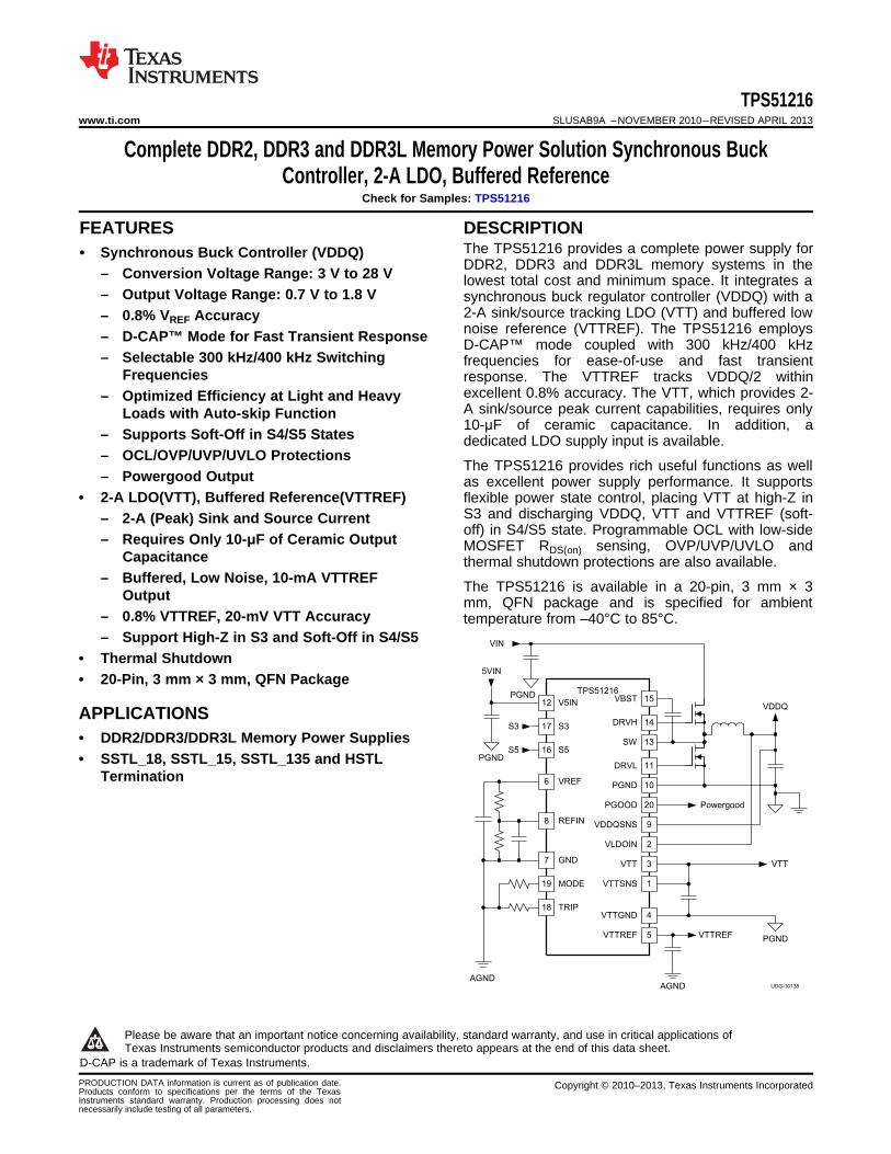
1FEATURES DESCRIPTIONThe TPS51216 provides a complete power supply for
2• Synchronous Buck Controller (VDDQ)DDR2, DDR3 and DDR3L memory systems in the
– Conversion Voltage Range: 3 V to 28 V lowest total cost and minimum space. It integrates a– Output Voltage Range: 0.7 V to 1.8 V synchronous buck regulator controller (VDDQ) with a
2-A sink/source tracking LDO (VTT) and buffered low– 0.8% VREF Accuracynoise reference (VTTREF). The TPS51216 employs– D-CAP™ Mode for Fast Transient Response D-CAP™ mode coupled with 300 kHz/400 kHz
– Selectable 300 kHz/400 kHz Switching frequencies for ease-of-use and fast transientFrequencies response. The VTTREF tracks VDDQ/2 within
excellent 0.8% accuracy. The VTT, which provides 2-– Optimized Efficiency at Light and HeavyA sink/source peak current capabilities, requires onlyLoads with Auto-skip Function10-μF of ceramic capacitance. In addition, a
– Supports Soft-Off in S4/S5 States dedicated LDO supply input is available.– OCL/OVP/UVP/UVLO Protections
The TPS51216 provides rich useful functions as well– Powergood Output as excellent power supply performance. It supports
• 2-A LDO(VTT), Buffered Reference(VTTREF) flexible power state control, placing VTT at high-Z inS3 and discharging VDDQ, VTT and VTTREF (soft-– 2-A (Peak) Sink and Source Currentoff) in S4/S5 state. Programmable OCL with low-side
– Requires Only 10-μF of Ceramic Output MOSFET RDS(on) sensing, OVP/UVP/UVLO andCapacitance thermal shutdown protections are also available.
– Buffered, Low Noise, 10-mA VTTREFThe TPS51216 is available in a 20-pin, 3 mm × 3
Output mm, QFN package and is specified for ambient– 0.8% VTTREF, 20-mV VTT Accuracy temperature from –40°C to 85°C.– Support High-Z in S3 and Soft-Off in S4/S5
• Thermal Shutdown• 20-Pin, 3 mm × 3 mm, QFN Package
APPLICATIONS• DDR2/DDR3/DDR3L Memory Power Supplies• SSTL_18, SSTL_15, SSTL_135 and HSTL
Termination
1
Please be aware that an important notice concerning availability, standard warranty, and use in critical applications ofTexas Instruments semiconductor products and disclaimers thereto appears at the end of this data sheet.
2D-CAP is a trademark of Texas Instruments.
PRODUCTION DATA information is current as of publication date. Copyright © 2010–2013, Texas Instruments IncorporatedProducts conform to specifications per the terms of the TexasInstruments standard warranty. Production processing does notnecessarily include testing of all parameters.
TPS51216SLUSAB9A –NOVEMBER 2010–REVISED APRIL 2013 www.ti.com
These devices have limited built-in ESD protection. The leads should be shorted together or the device placed in conductive foamduring storage or handling to prevent electrostatic damage to the MOS gates.
ORDERING INFORMATION (1)
ORDERABLE DEVICE OUTPUT MINIMUMTA PACKAGE PINSNUMBER SUPPLY QUANTITY
TPS51216RUKR Tape and reel 3000–40°C to 85°C Plastic Quad Flat Pack (20 pin QFN) 20
TPS51216RUKT Mini reel 250
(1) For the most current package and ordering information see the Package Option Addendum at the end of this document, or see the TIweb site at www.ti.com.
ABSOLUTE MAXIMUM RATINGS (1)
over operating free-air temperature range (unless otherwise noted)
VALUE UNIT
MIN MAX
VBST –0.3 36
VBST (3) –0.3 6
SW –5 30
Input voltage range (2) VLDOIN, VDDQSNS, REFIN –0.3 3.6 V
VTTSNS –0.3 3.6
PGND, VTTGND –0.3 0.3
V5IN, S3, S5, TRIP, MODE –0.3 6
DRVH –5 36
DRVH (3) –0.3 6
DRVH (3) (duty cycle < 1%) –2.5 6
VTTREF, VREF –0.3 3.6Output voltage range (2) V
VTT –0.3 3.6
DRVL –0.3 6
DRVL (duty cycle < 1%) –2.5 6
PGOOD –0.3 6
Junction temperature range, TJ 125 °C
Storage temperature range, TSTG –55 150 °C
(1) Stresses beyond those listed under absolute maximum ratings may cause permanent damage to the device. These are stress ratingsonly and functional operation of the device at these or any other conditions beyond those indicated under recommended operatingconditions is not implied. Exposure to absolute-maximum-rated conditions for extended periods may affect device reliability.
(2) All voltage values are with respect to the network ground terminal unless otherwise noted.(3) Voltage values are with respect to the SW terminal.
THERMAL INFORMATIONTPS51216
THERMAL METRIC UNITSQFN (20) PINS
θJA Junction-to-ambient thermal resistance 94.1
θJCtop Junction-to-case (top) thermal resistance 58.1
θJB Junction-to-board thermal resistance 64.3°C/W
ψJT Junction-to-top characterization parameter 31.8
ψJB Junction-to-board characterization parameter 58.0
θJCbot Junction-to-case (bottom) thermal resistance 5.9
2 Submit Documentation Feedback Copyright © 2010–2013, Texas Instruments Incorporated
Product Folder Links :TPS51216
TPS51216www.ti.com SLUSAB9A –NOVEMBER 2010–REVISED APRIL 2013
RECOMMENDED OPERATING CONDITIONSMIN TYP MAX UNIT
Supply voltage V5IN 4.5 5.5 V
VBST –0.1 33.5
VBST (1) –0.1 5.5
SW -3 28
SW (2) –4.5 28Input voltage range V
VLDOIN, VDDQSNS, REFIN –0.1 3.5
VTTSNS –0.1 3.5
PGND, VTTGND –0.1 0.1
S3, S5, TRIP, MODE –0.1 5.5
DRVH –3 33.5
DRVH (1) –0.1 5.5
DRVH (2) –4.5 33.5
Output voltage range VTTREF, VREF –0.1 3.5 V
VTT –0.1 3.5
DRVL –0.1 5.5
PGOOD –0.1 5.5
TA Operating free-air temperature –40 85 °C
(1) Voltage values are with respect to the SW terminal.(2) This voltage should be applied for less than 30% of the repetitive period.
Copyright © 2010–2013, Texas Instruments Incorporated Submit Documentation Feedback 3
Product Folder Links :TPS51216

TPS51216SLUSAB9A –NOVEMBER 2010–REVISED APRIL 2013 www.ti.com
ELECTRICAL CHARACTERISTICSover operating free-air temperature range, VV5IN=5V, VLDOIN is connected to VDDQ output, VMODE=0V, VS3=VS5=5V (unlessotherwise noted)
PARAMETER TEST CONDITION MIN TYP MAX UNIT
SUPPLY CURRENT
IV5IN(S0) V5IN supply current, in S0 TA = 25°C, No load, VS3 = VS5 = 5 V 590 μA
IV5IN(S3) V5IN supply current, in S3 TA = 25°C, No load, VS3 = 0 V, VS5 = 5 V 500 μA
IV5INSDN V5IN shutdown current TA = 25°C, No load, VS3 = VS5 = 0 V 1 μA
IVLDOIN(S0) VLDOIN supply current, in S0 TA = 25°C, No load, VS3 = VS5 = 5 V 5 μA
IVLDOIN(S3) VLDOIN supply current, in S3 TA = 25°C, No load, VS3 = 0 V, VS5 = 5 V 5 μA
IVLDOINSDN VLDOIN shutdown current TA = 25°C, No load, VS3 = VS5 = 0 V 5 μA
VREF OUTPUT
IVREF = 30 μA, TA = 25°C 1.8000
VVREF Output voltage 0 μA ≤ IVREF <300 μA, TA = –10°C to 85°C 1.7856 1.8144 V
0 μA ≤ IVREF <300 μA, TA = –40°C to 85°C 1.7820 1.8180
IVREFOCL Current limit VVREF = 1.7 V 0.4 0.8 mA
VTTREF OUTPUT
VVTTREF Output voltage VVDDQSNS/2 V
|IVTTREF| <100 μA, 1.2 V ≤ VVDDQSNS ≤ 1.8 V 49.2% 50.8%VVTTREF Output voltage tolerance to VVDDQ
|IVTTREF| <10 mA, 1.2 V ≤ VVDDQSNS ≤ 1.8 V 49% 51%
IVTTREFOCLSRC Source current limit VVDDQSNS = 1.8 V, VVTTREF= 0 V 10 18 mA
IVTTREFOCLSNK Sink current limit VVDDQSNS = 1.8 V, VVTTREF = 1.8 V 10 17 mA
IVTTREFDIS VTTREF discharge current TA = 25°C, VS3 = VS5 = 0 V, VVTTREF = 0.5 V 0.8 1.3 mA
VTT OUTPUT
VVTT Output voltage VVTTREF V
|IVTT| ≤ 10 mA, 1.2 V ≤ VVDDQSNS ≤ 1.8 V, IVTTREF = 0 A –20 20
|IVTT| ≤ 1 A, 1.2 ≤ VVDDQSNS ≤ 1.8 V, IVTTREF = 0 A –30 30VVTTTOL Output voltage tolerance to VTTREF mV
|IVTT| ≤ 2 A, 1.4 V ≤ VVDDQSNS ≤ 1.8 V, IVTTREF = 0 A –40 40
|IVTT| ≤ 1.5 A, 1.2 V ≤ VVDDQSNS ≤ 1.4 V, IVTTREF = 0 A –40 40
VVDDQSNS = 1.8 V, VVTT = VVTTSNS = 0.7 V,IVTTOCLSRC Source current limit 2 3IVTTREF = 0 A AIVTTOCLSNK Sink current limit VVDDQSNS = 1.8V, VVTT = VVTTSNS = 1.1 V, IVTTREF = 0 A 2 3
IVTTLK Leakage current TA = 25°C , VS3 = 0 V, VS5 = 5 V, VVTT = VVTTREF 5
IVTTSNSBIAS VTTSNS input bias current VS3 = 5 V, VS5 = 5 V, VVTTSNS = VVTTREF –0.5 0.0 0.5 μA
IVTTSNSLK VTTSNS leakage current VS3 = 0 V, VS5 = 5 V, VVTTSNS = VVTTREF –1 0 1
TA = 25°C, VS3 = VS5 = 0 V, VVDDQSNS = 1.8 V,IVTTDIS VTT Discharge current 7.8 mAVVTT = 0.5 V, IVTTREF = 0 A
VDDQ OUTPUT
VVDDQSNS VDDQ sense voltage VREFIN
VDDQSNS regulation voltageVVDDQSNSTOL TA = 25°C –3 3 mVtolerance to REFIN
IVDDQSNS VDDQSNS input current VVDDQSNS = 1.8 V 39 μA
IREFIN REFIN input current VREFIN = 1.8 V –0.1 0.0 0.1 μA
VS3 = VS5 = 0 V, VVDDQSNS = 0.5 V, MODE pin pulledIVDDQDIS VDDQ discharge current 12 mAdown to GND through 47kΩ (Non-tracking)
VS3 = VS5 = 0 V, VVDDQSNS = 0.5 V, MODE pin pulledIVLDOINDIS VLDOIN discharge current 1.2 Adown to GND through 100kΩ (Non-tracking)
SWITCH MODE POWER SUPPLY (SMPS) FREQUENCY
VIN = 12 V, VVDDQSNS = 1.8 V, RMODE = 100 kΩ 300fSW VDDQ switching frequency kHz
VIN = 12 V, VVDDQSNS = 1.8 V, RMODE = 200 kΩ 400
tON(min) Minimum on time DRVH rising to falling (1) 60ns
tOFF(min) Minimum off time DRVH falling to rising 200 320 450
(1) Ensured by design. Not production tested.
4 Submit Documentation Feedback Copyright © 2010–2013, Texas Instruments Incorporated
Product Folder Links :TPS51216

TPS51216www.ti.com SLUSAB9A –NOVEMBER 2010–REVISED APRIL 2013
ELECTRICAL CHARACTERISTICS (continued)over operating free-air temperature range, VV5IN=5V, VLDOIN is connected to VDDQ output, VMODE=0V, VS3=VS5=5V (unlessotherwise noted)
PARAMETER TEST CONDITION MIN TYP MAX UNIT
VDDQ MOSFET DRIVER
Source, IDRVH = –50 mA 1.6 3.0RDRVH DRVH resistance
Sink, IDRVH = 50 mA 0.6 1.5Ω
Source, IDRVL = –50 mA 0.9 2.0RDRVL DRVL resistance
Sink, IDRVL = 50 mA 0.5 1.2
DRVH-off to DRVL-on 10tDEAD Dead time ns
DRVL-off to DRVH-on 20
INTERNAL BOOT STRAP SW
VFBST Forward Voltage VV5IN-VBST, TA = 25°C, IF = 10 mA 0.1 0.2 V
IVBSTLK VBST leakage current TA = 25°C, VVBST = 33 V, VSW = 28 V 0.01 1.5 μA
LOGIC THRESHOLD
IMODE MODE source current 14 15 16 μA
MODE 0 580 600 620
MODE 1 829 854 879VTHMODE MODE threshold voltage mV
MODE 2 1202 1232 1262
MODE 3 1760 1800 1840
VIL S3/S5 low-level voltage 0.5
VIH S3/S5 high-level voltage 1.8 V
VIHYST S3/S5 hysteresis voltage 0.25
VILK S3/S5 input leak current –1 0 1 μA
SOFT START
Internal soft-start time, CVREF = 0.1 μF,tSS VDDQ soft-start time 1.1 msS5 rising to VVDDQSNS > 0.99 × VREFIN
PGOOD COMPARATOR
PGOOD in from higher 106% 108% 110%
PGOOD in from lower 90% 92% 94%VTHPG VDDQ PGOOD threshold
PGOOD out to higher 114% 116% 118%
PGOOD out to lower 82% 84% 86%
IPG PGOOD sink current VPGOOD = 0.5 V 3 5.9 mA
Delay for PGOOD in 0.8 1 1.2 mstPGDLY PGOOD delay time
Delay for PGOOD out, with 100 mV over drive 330 ns
tPGSSDLY PGOOD start-up delay CVREF = 0.1 μF, S5 rising to PGOOD rising 2.5 ms
Copyright © 2010–2013, Texas Instruments Incorporated Submit Documentation Feedback 5
Product Folder Links :TPS51216

TPS51216SLUSAB9A –NOVEMBER 2010–REVISED APRIL 2013 www.ti.com
ELECTRICAL CHARACTERISTICS (continued)over operating free-air temperature range, VV5IN=5V, VLDOIN is connected to VDDQ output, VMODE=0V, VS3=VS5=5V (unlessotherwise noted)
PARAMETER TEST CONDITION MIN TYP MAX UNIT
PROTECTIONS
ITRIP TRIP source current TA = 25°C, VTRIP = 0.4 V 9 10 11 μA
TRIP source current temperatureTCITRIP 4700 ppm/°Ccoefficient (2)
VTRIP VTRIP voltage range 0.2 3 V
VTRIP = 3.0 V 360 375 390
VOCL Current limit threshold VTRIP = 1.6 V 190 200 210 mV
VTRIP = 0.2 V 20 25 30
VTRIP = 3.0 V –390 –375 –360
VOCLN Negative current limit threshold VTRIP = 1.6 V –210 –200 –190 mV
VTRIP = 0.2 V –30 –25 –20
VZC Zero cross detection offset 0 mV
Wake-up 4.2 4.4 4.5VUVLO V5IN UVLO threshold voltage V
Shutdown 3.7 3.9 4.1
VOVP VDDQ OVP threshold voltage OVP detect voltage 118% 120% 122%
tOVPDLY VDDQ OVP propagation delay With 100 mV over drive 430 ns
VUVP VDDQ UVP threshold voltage UVP detect voltage 66% 68% 70%
tUVPDLY VDDQ UVP delay 1 ms
tUVPENDLY VDDQ UVP enable delay 1.2 ms
VOOB OOB Threshold voltage 108%
THERMAL SHUTDOWN
Shutdown temperature (2) 140TSDN Thermal shutdown threshold °C
Hysteresis (2) 10
(2) Ensured by design. Not production tested.
6 Submit Documentation Feedback Copyright © 2010–2013, Texas Instruments Incorporated
Product Folder Links :TPS51216

1
2
3
4
5
6 7 8 9 10
11
12
13
14
15
1617181920
TPS51216
PowerPAD™
VTTSNS
VLDOIN
VTT
VTTGND
VTTREF
VR
EF
GN
D
RE
FIN
VD
DQ
SN
S
PG
ND
DRVL
V5IN
SW
DRVH
VBST
S5
S3
TR
IP
MO
DE
PG
OO
D
TPS51216www.ti.com SLUSAB9A –NOVEMBER 2010–REVISED APRIL 2013
DEVICE INFORMATION
RUK PACKAGE (TOP VIEW)
PIN FUNCTIONSPIN
I/O DESCRIPTIONNAME NO.
DRVH 14 O High-side MOSFET gate driver output.
DRVL 11 O Low-side MOSFET gate driver output.
GND 7 – Signal ground.
MODE 19 I Connect resistor to GND to configure switching frequency and discharge mode. (See Table 2)
PGND 10 – Gate driver power ground. RDS(on) current sensing input(+).
PGOOD 20 O Powergood signal open drain output. PGOOD goes high when VDDQ output voltage is within the target range.
Reference input for VDDQ. Connect to the midpoint of a resistor divider from VREF to GND. Add a capacitor forREFIN 8 I stable operation.
SW 13 I/O High-side MOSFET gate driver return. RDS(on) current sensing input(–).
S3 17 I S3 signal input. (See Table 1)
S5 16 I S5 signal input. (See Table 1)
TRIP 18 I Connect resistor to GND to set OCL at VTRIP/8. Output 10-μA current at room temperature, TC = 4700 ppm/°C.
VBST 15 I High-side MOSFET gate driver bootstrap voltage input. Connect a capacitor from the VBST pin to the SW pin.
VDDQSNS 9 I VDDQ output voltage feedback. Reference input for VTTREF. Also serves as power supply for VTTREF.
VLDOIN 2 I Power supply input for VTT LDO. Connect VDDQ in typical application.
VREF 6 O 1.8-V reference output.
VTT 3 O VTT 2-A LDO output. Need to connect 10μF or larger capacitance for stability.
VTTGND 4 – Power ground for VTT LDO.
VTTREF 5 O Buffered VTT reference output. Need to connect 0.22μF or larger capacitance for stability.
VTTSNS 1 I VTT output voltage feedback.
V5IN 12 I 5-V power supply input for internal circuits and MOSFET gate drivers.
Thermal – – Connect to GNDpad
Copyright © 2010–2013, Texas Instruments Incorporated Submit Documentation Feedback 7
Product Folder Links :TPS51216
10
13
PGND
SW
TPS51216
OC
ZC
XCON
15 VBST
12 V5IN
PWM
9
REFIN
TRIP
Delay
20 PGOOD
Control Logic
UDG-10135
10 mA
+
+
VREFIN
+20%
+
+
8
VDDQSNS
++
18
14 DRVH
11 DRVL
tON
One-
Shot
UV
OV
VREFIN
–32%
16S5
Soft-Start
+NOC
+
8 R
6VREF Reference
R
7GND
17S3
5VTTREF
1VTTSNS
4 VTTGND
3 VTT
+
+
+
+ 2 VLDOIN
7 R
R
VTT Discharge
VTTREF Discharge
On-Time
Discharge Type
Selection
15 mA
19 MODE
VREFIN
+8/16 %
VREFIN
–8/16 %
+
+
VDDQ
Discharge V5OK
+
4.4 V/3.9 V
UVP
OVP
TPS51216SLUSAB9A –NOVEMBER 2010–REVISED APRIL 2013 www.ti.com
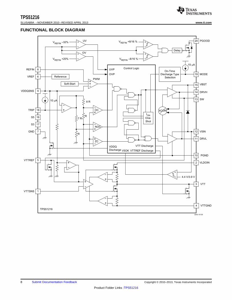
FUNCTIONAL BLOCK DIAGRAM
8 Submit Documentation Feedback Copyright © 2010–2013, Texas Instruments Incorporated
Product Folder Links :TPS51216
50
60
70
80
90
100
110
120
130
140
150
−50 −25 0 25 50 75 100 125Junction Temperature (°C)
OV
P/U
VP
Thr
esho
ld (
%)
OVPUVP
0
3
6
9
12
15
−50 −25 0 25 50 75 100 125Junction Temperature (°C)
VD
DQ
SN
S D
isch
arge
Cur
rent
(m
A)
0
2
4
6
8
10
−50 −25 0 25 50 75 100 125Junction Temperature (°C)
VLD
OIN
Sup
py C
urre
nt (
µA)
4
6
8
10
12
14
16
−50 −25 0 25 50 75 100 125Junction Temperature (°C)
TR
IP S
ourc
e C
urre
nt (
µA)
0
200
400
600
800
1000
−50 −25 0 25 50 75 100 125Junction Temperature (°C)
V5I
N S
uppy
Cur
rent
(µA
)
0
2
4
6
8
10
−50 −25 0 25 50 75 100 125Junction Temperature (°C)
V5I
N S
hutd
own
Cur
rent
(µA
)
TPS51216www.ti.com SLUSAB9A –NOVEMBER 2010–REVISED APRIL 2013
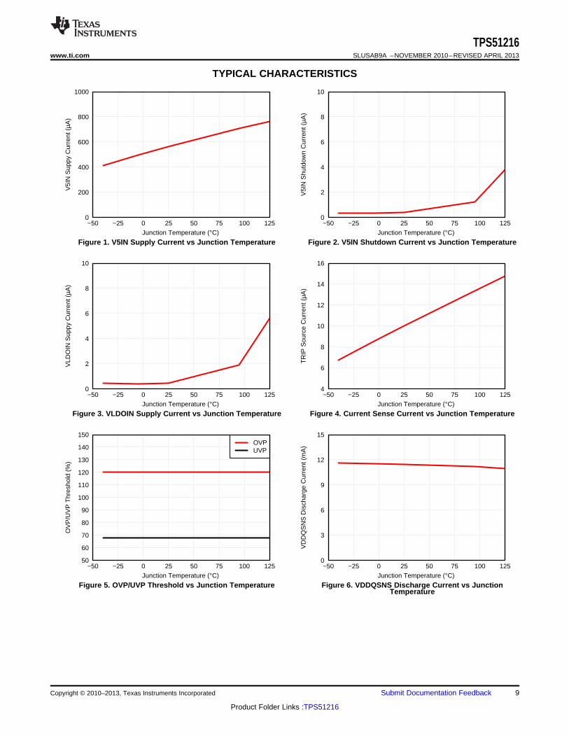
TYPICAL CHARACTERISTICS
Figure 1. V5IN Supply Current vs Junction Temperature Figure 2. V5IN Shutdown Current vs Junction Temperature
Figure 3. VLDOIN Supply Current vs Junction Temperature Figure 4. Current Sense Current vs Junction Temperature
Figure 5. OVP/UVP Threshold vs Junction Temperature Figure 6. VDDQSNS Discharge Current vs JunctionTemperature
Copyright © 2010–2013, Texas Instruments Incorporated Submit Documentation Feedback 9
Product Folder Links :TPS51216
0
100
200
300
400
500
600
700
800
0 2 4 6 8 10 12 14 16 18 20VDDQ Output Current (A)
Sw
itchi
ng F
requ
ency
(kH
z)
VVDDQ = 1.20 VVVDDQ = 1.35 VVVDDQ = 1.50 V
RMODE = 200 kΩVIN = 12 V
1.45
1.46
1.47
1.48
1.49
1.50
1.51
1.52
1.53
1.54
1.55
0 2 4 6 8 10 12 14 16 18 20VDDQ Output Current (A)
VD
DQ
Out
put V
olta
ge (
V)
RMODE = 200 kΩVIN = 12 V
200
300
400
500
600
700
800
6 8 10 12 14 16 18 20 22Input Voltage (V)
Sw
itchi
ng F
requ
ency
(kH
z)
VVDDQ = 1.20 VVVDDQ = 1.35 VVVDDQ = 1.50 V
RMODE = 200 kΩIVDDQ = 10 A
0
100
200
300
400
500
600
700
800
0 2 4 6 8 10 12 14 16 18 20VDDQ Output Current (A)
Sw
itchi
ng F
requ
ency
(kH
z)
VVDDQ = 1.20 VVVDDQ = 1.35 VVVDDQ = 1.50 V
RMODE = 100 kΩVIN = 12 V
0
2
4
6
8
10
−50 −25 0 25 50 75 100 125Junction Temperature (°C)
VT
T D
isch
arge
Cur
rent
(m
A)
200
300
400
500
600
700
800
6 8 10 12 14 16 18 20 22Input Voltage (V)
Sw
itchi
ng F
requ
ency
(kH
z)
VVDDQ = 1.20 VVVDDQ = 1.35 VVVDDQ = 1.50 V
RMODE = 100 kΩIVDDQ = 10 A
TPS51216SLUSAB9A –NOVEMBER 2010–REVISED APRIL 2013 www.ti.com
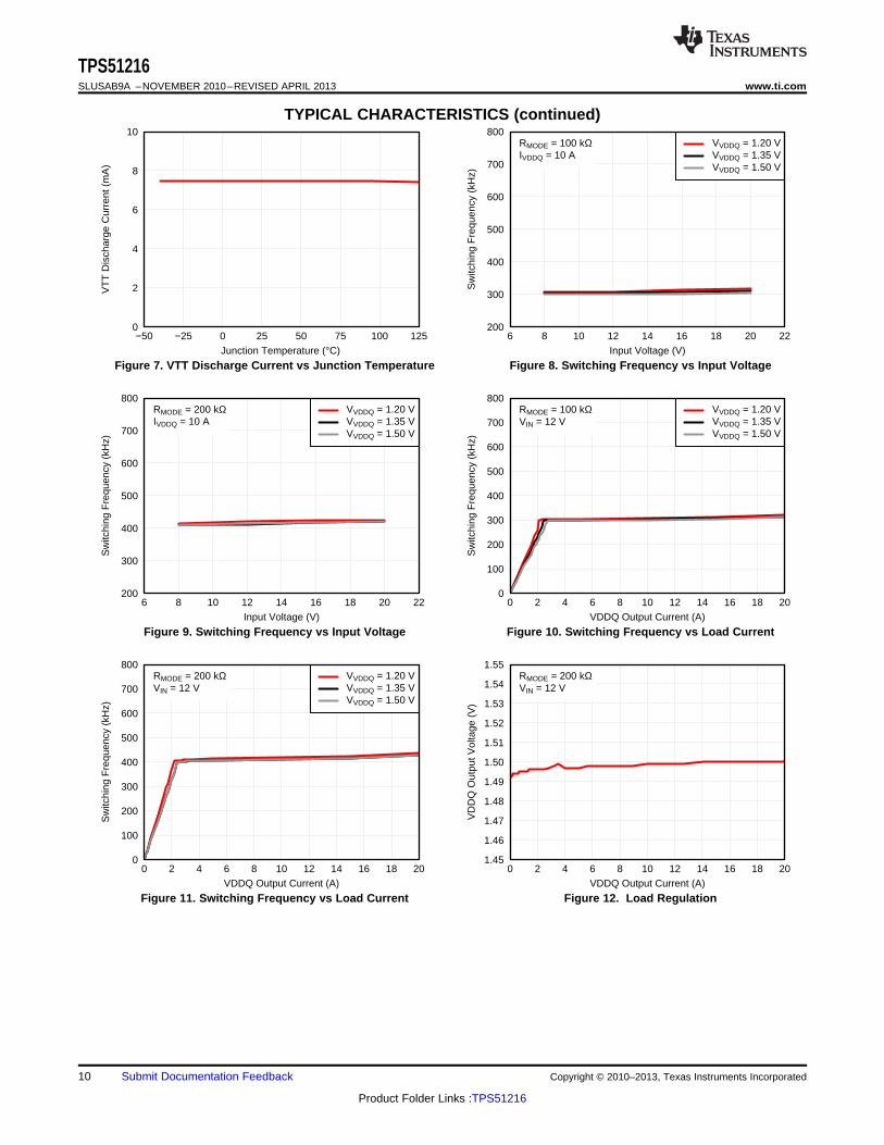
TYPICAL CHARACTERISTICS (continued)
Figure 7. VTT Discharge Current vs Junction Temperature Figure 8. Switching Frequency vs Input Voltage
Figure 9. Switching Frequency vs Input Voltage Figure 10. Switching Frequency vs Load Current
Figure 11. Switching Frequency vs Load Current Figure 12. Load Regulation
10 Submit Documentation Feedback Copyright © 2010–2013, Texas Instruments Incorporated
Product Folder Links :TPS51216

0.710
0.720
0.730
0.740
0.750
0.760
0.770
0.780
0.790
−2.0 −1.5 −1.0 −0.5 0.0 0.5 1.0 1.5 2.0VTT Current (V)
VT
T V
olta
ge (
V)
VVDDQ = 1.5 V0.635
0.645
0.655
0.665
0.675
0.685
0.695
0.705
0.715
−2.0 −1.5 −1.0 −0.5 0.0 0.5 1.0 1.5 2.0VTT Current (V)
VT
T V
olta
ge (
V)
VVDDQ = 1.35 V
0.650
0.655
0.660
0.665
0.670
0.675
0.680
0.685
0.690
0.695
−10 −5 0 5 10VTTREF Current (mA)
VT
TR
EF
Vol
tage
(V
)
VVDDQ = 1.35 V0.580
0.585
0.590
0.595
0.600
0.605
0.610
0.615
0.620
−10 −5 0 5 10VTTREF Current (mA)
VT
TR
EF
Vol
tage
(V
)
VVDDQ = 1.2 V
1.45
1.46
1.47
1.48
1.49
1.50
1.51
1.52
1.53
1.54
1.55
6 8 10 12 14 16 18 20 22Input Voltage (V)
VD
DQ
Out
put V
olta
ge (
V)
IVDDQ = 0 AIVDDQ = 20 A
RMODE = 200 kΩ
0.730
0.735
0.740
0.745
0.750
0.755
0.760
0.765
0.770
−10 −5 0 5 10VTTREF Current (mA)
VT
TR
EF
Vol
tage
(V
)
VVDDQ = 1.5 V
TPS51216www.ti.com SLUSAB9A –NOVEMBER 2010–REVISED APRIL 2013
TYPICAL CHARACTERISTICS (continued)
Figure 13. Line Regulation Figure 14. VTTREF Load Regulation
Figure 15. VTTREF Load Regulation Figure 16. VTTREF Load Regulation
Figure 17. VTT Load Regulation Figure 18. VTT Load Regulation
Copyright © 2010–2013, Texas Instruments Incorporated Submit Documentation Feedback 11
Product Folder Links :TPS51216

0.560
0.570
0.580
0.590
0.600
0.610
0.620
0.630
0.640
−2.0 −1.5 −1.0 −0.5 0.0 0.5 1.0 1.5 2.0VTT Current (V)
VT
T V
olta
ge (
V)
VVDDQ = 1.2 V0
10
20
30
40
50
60
70
80
90
100
0.001 0.01 0.1 1 10 100VDDQ Output Current (A)
Effi
cien
cy (
%)
VIN = 20 VVIN = 12 VVIN = 8 V
VVDDQ = 1.5 VRMODE = 200 kΩ
TPS51216SLUSAB9A –NOVEMBER 2010–REVISED APRIL 2013 www.ti.com
TYPICAL CHARACTERISTICS (continued)
Figure 19. VTT Load Regulation Figure 20. Efficiency
Figure 21. 1.5-V Load Transient Response Figure 22. VTT Load Transient Response
12 Submit Documentation Feedback Copyright © 2010–2013, Texas Instruments Incorporated
Product Folder Links :TPS51216
TPS51216www.ti.com SLUSAB9A –NOVEMBER 2010–REVISED APRIL 2013
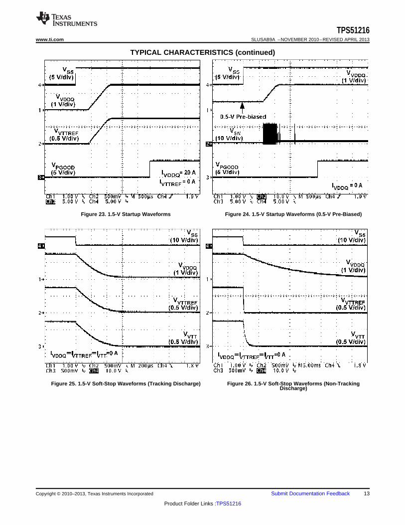
TYPICAL CHARACTERISTICS (continued)
Figure 23. 1.5-V Startup Waveforms Figure 24. 1.5-V Startup Waveforms (0.5-V Pre-Biased)
Figure 25. 1.5-V Soft-Stop Waveforms (Tracking Discharge) Figure 26. 1.5-V Soft-Stop Waveforms (Non-TrackingDischarge)
Copyright © 2010–2013, Texas Instruments Incorporated Submit Documentation Feedback 13
Product Folder Links :TPS51216
10000 100000 1000000 10000000−80
−60
−40
−20
0
20
40
60
80
−180
−135
−90
−45
0
45
90
135
180
Frequency (Hz)
Gai
n (d
B)
Pha
se (
°)
GainPhaseIVTT = −1 A
10000 100000 1000000 10000000−80
−60
−40
−20
0
20
40
60
80
−180
−135
−90
−45
0
45
90
135
180
Frequency (Hz)
Gai
n (d
B)
Pha
se (
°)
GainPhaseIVTT = 1 A
TPS51216SLUSAB9A –NOVEMBER 2010–REVISED APRIL 2013 www.ti.com
TYPICAL CHARACTERISTICS (continued)
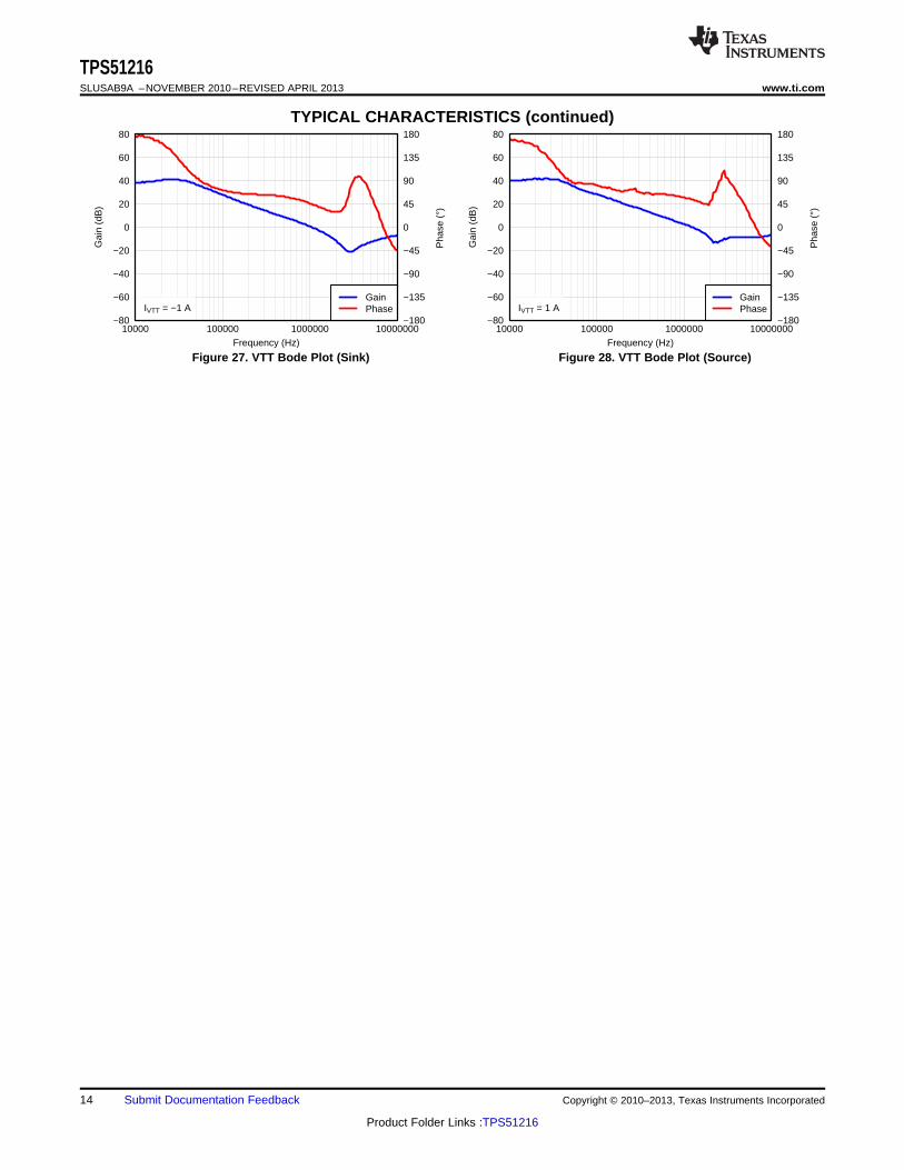
Figure 27. VTT Bode Plot (Sink) Figure 28. VTT Bode Plot (Source)
14 Submit Documentation Feedback Copyright © 2010–2013, Texas Instruments Incorporated
Product Folder Links :TPS51216
700 ms400 ms 1.4 ms
S5
VREF
VDDQ
PGOOD
UDG-10137
TPS51216www.ti.com SLUSAB9A –NOVEMBER 2010–REVISED APRIL 2013
APPLICATION INFORMATION
VDDQ Switch Mode Power Supply Control
TPS51216 supports D-CAP™ mode which does not require complex external compensation networks and issuitable for designs with small external components counts. The D-CAP™ mode provides fast transient responsewith appropriate amount of equivalent series resistance (ESR) on the output capacitors. An adaptive on-timecontrol scheme is used to achieve pseudo-constant frequency. The TPS51216 adjusts the on-time (tON) to beinversely proportional to the input voltage (VIN) and proportional to the output voltage (VDDQ). This makes aswitching frequency fairy constant over the variation of input voltage at the steady state condition.
VREF and REFIN, VDDQ Output Voltage
The part provides a 1.8-V, ±0.8% accurate, voltage reference from VREF. This output has a 300-μA (max)current capability to drive the REFIN input voltage through a voltage divider circuit. A capacitor with a value of0.1-μF or larger should be attached close to the VREF terminal.
The VDDQ switch-mode power supply (SMPS) output voltage is defined by REFIN voltage, within the rangebetween 0.7 V and 1.8 V, programmed by the resister-divider connected between VREF and GND. (See ExternalComponents Selection section.) A few nano farads of capacitance from REFIN to GND is recommended forstable operation.
Soft-Start and Powergood
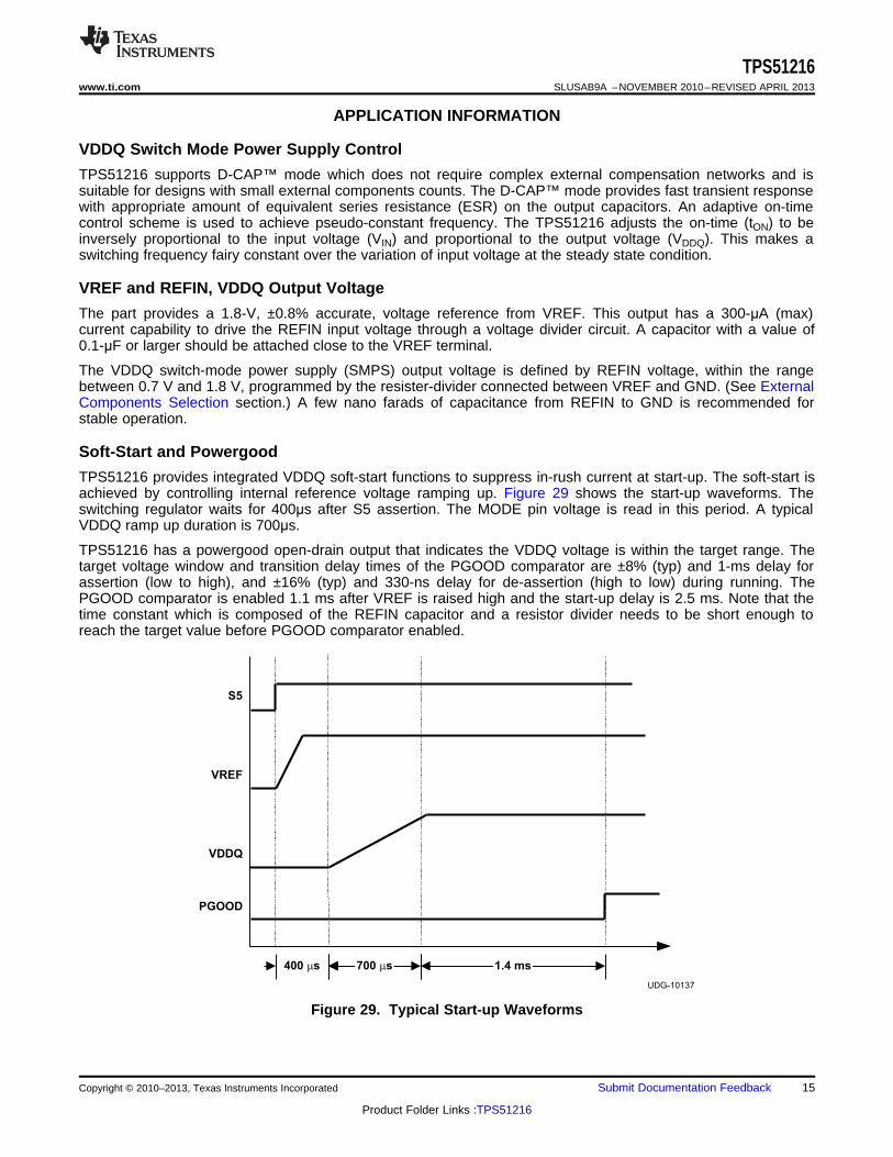
TPS51216 provides integrated VDDQ soft-start functions to suppress in-rush current at start-up. The soft-start isachieved by controlling internal reference voltage ramping up. Figure 29 shows the start-up waveforms. Theswitching regulator waits for 400μs after S5 assertion. The MODE pin voltage is read in this period. A typicalVDDQ ramp up duration is 700μs.
TPS51216 has a powergood open-drain output that indicates the VDDQ voltage is within the target range. Thetarget voltage window and transition delay times of the PGOOD comparator are ±8% (typ) and 1-ms delay forassertion (low to high), and ±16% (typ) and 330-ns delay for de-assertion (high to low) during running. ThePGOOD comparator is enabled 1.1 ms after VREF is raised high and the start-up delay is 2.5 ms. Note that thetime constant which is composed of the REFIN capacitor and a resistor divider needs to be short enough toreach the target value before PGOOD comparator enabled.
Figure 29. Typical Start-up Waveforms
Copyright © 2010–2013, Texas Instruments Incorporated Submit Documentation Feedback 15
Product Folder Links :TPS51216
TPS51216SLUSAB9A –NOVEMBER 2010–REVISED APRIL 2013 www.ti.com
Power State Control
The TPS51216 has two input pins, S3 and S5, to provide simple control scheme of power state. All of VDDQ,VTTREF and VTT are turned on at S0 state (S3=S5=high). In S3 state (S3=low, S5=high), VDDQ and VTTREFvoltages are kept on while VTT is turned off and left at high impedance state (high-Z). The VTT output floats anddoes not sink or source current in this state. In S4/S5 states (S3=S5=low), all of the three outputs are turned offand discharged to GND according to the discharge mode selected by MODE pin. Each state code represents asfollow; S0 = full ON, S3 = suspend to RAM (STR), S4 = suspend to disk (STD), S5 = soft OFF. (See Table 1)
Table 1. S3/S5 Power State Control
STATE S3 S5 VREF VDDQ VTTREF VTT
S0 HI HI ON ON ON ON
S3 LO HI ON ON ON OFF(High-Z)
S4/S5 LO LO OFF OFF(Discharge) OFF(Discharge) OFF(Discharge)
MODE Pin Configuration
The TPS51216 reads the MODE pin voltage when the S5 signal is raised high and stores the status in a register.A 15-μA current is sourced from the MODE pin during this time to read the voltage across the resistor connectedbetween the pin and GND. Table 2 shows resistor values, corresponding switching frequency and dischargemode configurations.
Table 2. MODE Selection
RESISTANCE BETWEEN SWITCHINGMODE NO. DISCHARGE MODEMODE AND GND ( kΩ) FREQUENCY (kHz)
3 200 400 Tracking
2 100 300
1 68 300 Non-tracking
0 47 400
Discharge Control
In S4/S5 state, VDDQ, VTT, and VTTREF outputs are discharged based on the respective discharge modeselected above. The tracking discharge mode discharges VDDQ output through the internal VTT regulatortransistors enabling quick discharge operation. The VTT output maintains tracking of the VTTREF voltage in thismode. (Please refer to Figure 25) After 4 ms of tracking discharge operation, the mode changes to non-trackingdischarge. The VDDQ output must be connected to the VLDOIN pin in this mode. The non-tracking modedischarges the VDDQ and VTT pins using internal MOSFETs that are connected to corresponding outputterminals. The non-tracking discharge is slow compared with the tracking discharge due to the lower currentcapability of these MOSFETs. (Please refer to Figure 26)
16 Submit Documentation Feedback Copyright © 2010–2013, Texas Instruments Incorporated
Product Folder Links :TPS51216
= £
p ´ ´
SW0
OUT
f1f
2 ESR C 3
9
+
8
PWM
VDDQSNS
REFIN
6
VREF
Control
Logic
and
DriverR1
R2
14
11
DRVH
DRVL
+1.8 V
VIN
Lx
ESR
COUT
RLOAD
UDG-10136
High-Side
MOSFET
Low-Side
MOSFET
VDDQ
TPS51216www.ti.com SLUSAB9A –NOVEMBER 2010–REVISED APRIL 2013
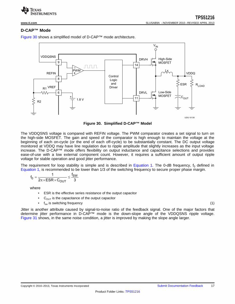
D-CAP™ Mode
Figure 30 shows a simplified model of D-CAP™ mode architecture.
Figure 30. Simplified D-CAP™ Model
The VDDQSNS voltage is compared with REFIN voltage. The PWM comparator creates a set signal to turn onthe high-side MOSFET. The gain and speed of the comparator is high enough to maintain the voltage at thebeginning of each on-cycle (or the end of each off-cycle) to be substantially constant. The DC output voltagemonitored at VDDQ may have line regulation due to ripple amplitude that slightly increases as the input voltageincrease. The D-CAP™ mode offers flexibility on output inductance and capacitance selections and providesease-of-use with a low external component count. However, it requires a sufficient amount of output ripplevoltage for stable operation and good jitter performance.
The requirement for loop stability is simple and is described in Equation 1. The 0-dB frequency, f0 defined inEquation 1, is recommended to be lower than 1/3 of the switching frequency to secure proper phase margin.
where• ESR is the effective series resistance of the output capacitor• COUT is the capacitance of the output capacitor• fsw is switching frequency (1)
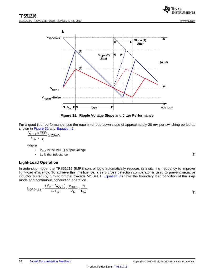
Jitter is another attribute caused by signal-to-noise ratio of the feedback signal. One of the major factors thatdetermine jitter performance in D-CAP™ mode is the down-slope angle of the VDDQSNS ripple voltage.Figure 31 shows, in the same noise condition, a jitter is improved by making the slope angle larger.
Copyright © 2010–2013, Texas Instruments Incorporated Submit Documentation Feedback 17
Product Folder Links :TPS51216
( )-= ´ ´
´
IN OUT OUTLOAD(LL)
X IN SW
V V V 1I
2 L V f
´³
´
OUT
SW X
V ESR20mV
f L
VVDDQSNS
VREFIN
(1)
(2)
tON
tOFF
Slope (2)
Jitter
20 mV
Slope (1)
Jitter
UDG-10139
VREFIN
+Noise
TPS51216SLUSAB9A –NOVEMBER 2010–REVISED APRIL 2013 www.ti.com
Figure 31. Ripple Voltage Slope and Jitter Performance
For a good jitter performance, use the recommended down slope of approximately 20 mV per switching period asshown in Figure 31 and Equation 2.
where• VOUT is the VDDQ output voltage• LX is the inductance (2)
Light-Load Operation
In auto-skip mode, the TPS51216 SMPS control logic automatically reduces its switching frequency to improvelight-load efficiency. To achieve this intelligence, a zero cross detection comparator is used to prevent negativeinductor current by turning off the low-side MOSFET. Equation 3 shows the boundary load condition of this skipmode and continuous conduction operation.
(3)
18 Submit Documentation Feedback Copyright © 2010–2013, Texas Instruments Incorporated
Product Folder Links :TPS51216
12
17
16
6
15
14
13
11
V5IN
TPS51216
S3
S5
VREF
VBST
DRVH
SW
DRVL
8
10
REFIN
PGND
7
19
GND
MODE
18 TRIP
20
9
2
3
PGOOD
VDDQSNS
VLDOIN
VTT
1
4
5
VTTSNS
VTTGND
VTTREF
UDG-13089
VDDQ
S5
PGND
5VIN
PGND
VIN
AGND
Powergood
PGND
1 kW
PGND
PGND
0.22 mF
AGND
TPS51216www.ti.com SLUSAB9A –NOVEMBER 2010–REVISED APRIL 2013
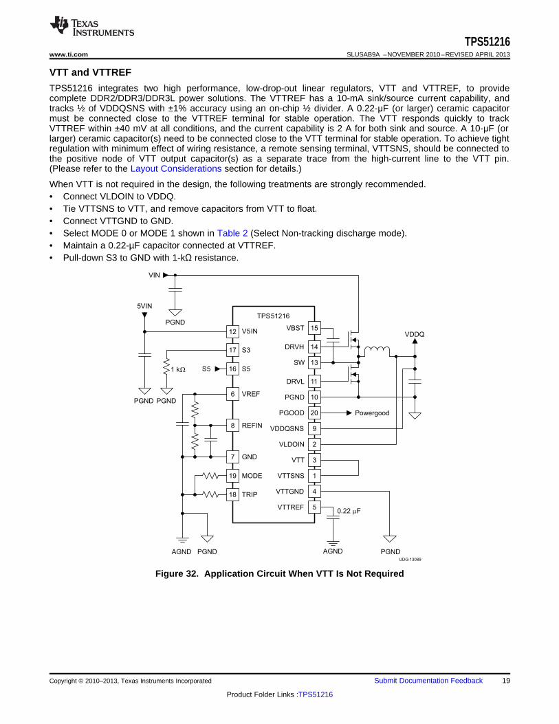
VTT and VTTREF
TPS51216 integrates two high performance, low-drop-out linear regulators, VTT and VTTREF, to providecomplete DDR2/DDR3/DDR3L power solutions. The VTTREF has a 10-mA sink/source current capability, andtracks ½ of VDDQSNS with ±1% accuracy using an on-chip ½ divider. A 0.22-μF (or larger) ceramic capacitormust be connected close to the VTTREF terminal for stable operation. The VTT responds quickly to trackVTTREF within ±40 mV at all conditions, and the current capability is 2 A for both sink and source. A 10-μF (orlarger) ceramic capacitor(s) need to be connected close to the VTT terminal for stable operation. To achieve tightregulation with minimum effect of wiring resistance, a remote sensing terminal, VTTSNS, should be connected tothe positive node of VTT output capacitor(s) as a separate trace from the high-current line to the VTT pin.(Please refer to the Layout Considerations section for details.)
When VTT is not required in the design, the following treatments are strongly recommended.• Connect VLDOIN to VDDQ.• Tie VTTSNS to VTT, and remove capacitors from VTT to float.• Connect VTTGND to GND.• Select MODE 0 or MODE 1 shown in Table 2 (Select Non-tracking discharge mode).• Maintain a 0.22-µF capacitor connected at VTTREF.• Pull-down S3 to GND with 1-kΩ resistance.
Figure 32. Application Circuit When VTT Is Not Required
Copyright © 2010–2013, Texas Instruments Incorporated Submit Documentation Feedback 19
Product Folder Links :TPS51216

( )
( )
( )
æ ö æ ö -ç ÷ ç ÷= + = + ´ ´ç ÷ ç ÷´ ´ ´è ø è ø
IND ripple IN OUT OUTTRIP TRIPOCL
X SW INDS on DS on
I V V VV V 1I
8 R 2 8 R 2 L f V
= ´TRIP TRIP TRIPV R I
TPS51216SLUSAB9A –NOVEMBER 2010–REVISED APRIL 2013 www.ti.com
VDDQ Overvoltage and Undervoltage Protection
TPS51216 sets the overvoltage protection (OVP) when the VDDQSNS voltage reaches a level 20% (typ) higherthan the REFIN voltage. When an OV event is detected, the controller latches DRVH low and DRVL high.VTTREF and VTT are turned off and discharged using the non-tracking discharge MOSFETs regardless of thetracking mode.
The undervoltage protection (UVP) latch is set when the VDDQSNS voltage remains lower than 68% (typ) of theREFIN voltage for 1 ms or longer. In this fault condition, the controller latches DRVH low and DRVL low anddischarges the VDDQ, VTT and VTTREF outputs. UVP detection function is enabled after 1.2 ms of SMPSoperation to ensure startup.
To release the OVP and UVP latches, toggle S5 or adjust the V5IN voltage down and up beyond theundervoltage lockout threshold.
VDDQ Overcurrent Protection
The VDDQ SMPS has cycle-by-cycle overcurrent limiting protection. The inductor current is monitored during theoff-state using the low-side MOSFET RDS(on) and the controller maintains the off-state while the voltage acrossthe low-side MOSFET is larger than the overcurrent trip level. The current monitor circuit inputs are PGND andSW pins so that those should be properly connected to the source and drain terminals of low-side MOSFET. Theovercurrent trip level, VTRIP, is determined by Equation 4, where RTRIP is the value of the resistor connectedbetween the TRIP pin and GND, and ITRIP is the current sourced from the TRIP pin. ITRIP is 10 μA typically atroom temperature, and has 4700ppm/°C temperature coefficient to compensate the temperature dependency ofthe low-side MOSFET RDS(on).
(4)
Because the comparison is done during the off-state, VTRIP sets the valley level of the inductor current. The loadcurrent OCL level, IOCL, can be calculated by considering the inductor ripple current as shown in Equation 5
where• IIND(ripple) is inductor ripple current (5)
In an overcurrent condition, the current to the load exceeds the current to the output capacitor, thus the outputvoltage tends to fall down. Eventually, it crosses the undervoltage protection threshold and shuts down.
VTT Overcurrent Protection
The LDO has an internally fixed constant overcurrent limiting of 3-A (typ) for both sink and source operation.
V5IN Undervoltage Lockout Protection
TPS51216 has a 5-V supply undervoltage lockout protection (UVLO) threshold. When the V5IN voltage is lowerthan UVLO threshold voltage, typically 3.93 V, VDDQ, VTT and VTTREF are shut off. This is a non-latchprotection.
Thermal Shutdown
TPS51216 includes an internal temperature monitor. If the temperature exceeds the threshold value, 140°C (typ),VDDQ, VTT and VTTREF are shut off. The thermal shutdown state of VDDQ is open, VTT and VTTREF are highimpedance (high-Z) respectively, and the discharge functions are disabled. This is a non-latch protection and theoperation is restarted with soft-start sequence when the device temperature is reduced by 10°C (typ).
20 Submit Documentation Feedback Copyright © 2010–2013, Texas Instruments Incorporated
Product Folder Links :TPS51216
´³
´
OUT
SW X
V ESR20mV
f L
£
p ´ ´
SW
OUT
f1
2 ESR C 3
( )( ) ( )
æ öæ ö-ç ÷´ - ´ ´ç ÷ç ÷ç ÷´ ´è øè ø=
IN OUT OUTOCL DS(on)
X SW IN
TRIPTRIP
V V V8 I R
2 L f VR
I
( )( )
( )( )( )
- ´= + ´
´ ´
IN OUT OUTmaxTRIP
IND peakX SW INDS on max
V V VV 1I
8 R L f V
( )
( )( )( ) ( )
( )( )( )
- ´ - ´= ´ = ´
´ ´
IN OUT OUT IN OUT OUTmax max
XSW IN O SW ININD ripple max max max
V V V V V V1 3
LI f V I f V
( )
=æ öç ÷ç ÷ç ÷ -
´æ öç ÷ç ÷-ç ÷ç ÷ç ÷è øè ø
IND ripple
OUT
R1R2
1.81
I ESRV
2
TPS51216www.ti.com SLUSAB9A –NOVEMBER 2010–REVISED APRIL 2013
External Components Selection
The external components selection is simple in D-CAP™ mode.1. DETERMINE THE VALUE OF R1 AND R2
The output voltage is determined by the value of the voltage-divider resistor, R1 and R2 as shown inFigure 30. R1 is connected between VREF and REFIN pins, and R2 is connected between the REFIN pinand GND. Setting R1 as 10-kΩ is a good starting point. Determine R2 using Equation 6.
(6)
2. CHOOSE THE INDUCTOR
The inductance value should be determined to yield a ripple current of approximately ¼ to ½ of maximumoutput current. Larger ripple current increases output ripple voltage and improves the signal-to-noise ratioand helps stable operation.
(7)
The inductor needs a low direct current resistance (DCR) to achieve good efficiency, as well as enough roomabove peak inductor current before saturation. The peak inductor current can be estimated in Equation 8.
(8)
3. CHOOSE THE OCL SETTING RESISTANCE, RTRIP
Combining Equation 4 and Equation 5, RTRIP can be obtained using Equation 9.
(9)
4. CHOOSE THE OUTPUT CAPACITORS
Organic semiconductor capacitor(s) or specialty polymer capacitor(s) are recommended. Determine ESR tomeet small signal stability and recommended ripple voltage. A quick reference is shown in Equation 10 andEquation 11.
(10)
(11)
Copyright © 2010–2013, Texas Instruments Incorporated Submit Documentation Feedback 21
Product Folder Links :TPS51216

´ ´³ ³
p ´ ´
SW
OUT SW OUT
20mV f L 3ESR or ESR
V 2 f C
1
2
3
4
15
14
13
12
VTTSNS
U1
TPS51216RUK
VLDOIN
VTT
VTTGND
VBST
DRVH
SW
V5IN
5 11VTTREF DRVL
10987
PG
ND
VD
DQ
SN
S
RE
FIN
GN
D
6
VR
EF
16171819
S5
S3
TR
IP
MO
DE
20
PG
OO
D
21
Pw
Pad
C6
1 mF
UDG-10165
C7
0.1 mF
C8
10 mF
C9
10 mF
C10
10 mF
VIN
8 V to 20 V
PGND
R6
0 W
C5
0.1 mF
R7 0 W L1
0.56 mH
Q2
FDMS8670AS
Q3
FDMS8670AS C11
330 mF
VDDQ_GND
PGND AGNDR5
49 kW
R4
10 kW
C3
0.1 mF
C4
10 nF
C2
0.22 mF
C1
10 mF
C12
10 mF
PGND
VTT
0.75 V/2 A
VTTREF
0.75 V
VTTGND
S5S3
R1
100 kW
R2 200 kW
R3 36 kW
V5IN
4.5 V to 5.5 V
Q1
FDMS8680VDDQ
1.5 V/20 A
AGND
PGND
TPS51216SLUSAB9A –NOVEMBER 2010–REVISED APRIL 2013 www.ti.com
TPS51216 Application Circuit
Figure 33. DDR3, 400-kHz Application Circuit, Tracking Discharge
Table 3. DDR3, 400-kHz Application Circuit, List of Materials
REFERENCE QTY SPECIFICATION MANUFACTURE PART NUMBERDESIGNATOR
C8, C9, C10 3 10 µF, 25 V Taiyo Yuden TMK325BJ106MM
C11 1 330 µF, 2V, 6 mΩ Panasonic EEFSX0D331XE
L1 1 0.56 µH, 21 A, 1.56 mΩ Panasonic ETQP4LR56WFC
Q1 1 30 V, 35 A, 8.5 mΩ Fairchild FDMS8680
Q2, Q3 2 30 V, 42 A, 3.5 mΩ Fairchild FDMS8670AS
For this example, the bulk output capacitor ESR requirement for D-CAP™ mode is described in Equation 12,whichever is greater.
(12)
22 Submit Documentation Feedback Copyright © 2010–2013, Texas Instruments Incorporated
Product Folder Links :TPS51216
TPS51216
DRVL
11
VIN
REFIN GND
V5IN
12 VOUT
TRIP
MODE
10
7
PGND
VREF
19
18
4
3
VTT
UDG-10166
VTTGND
5
0.22 mF
VTTREF
2
86
10 mF
10 nF
0.1 mF
VTT
VTTGND
VLDOIN
1 mF
#1
#2
#3
TPS51216www.ti.com SLUSAB9A –NOVEMBER 2010–REVISED APRIL 2013
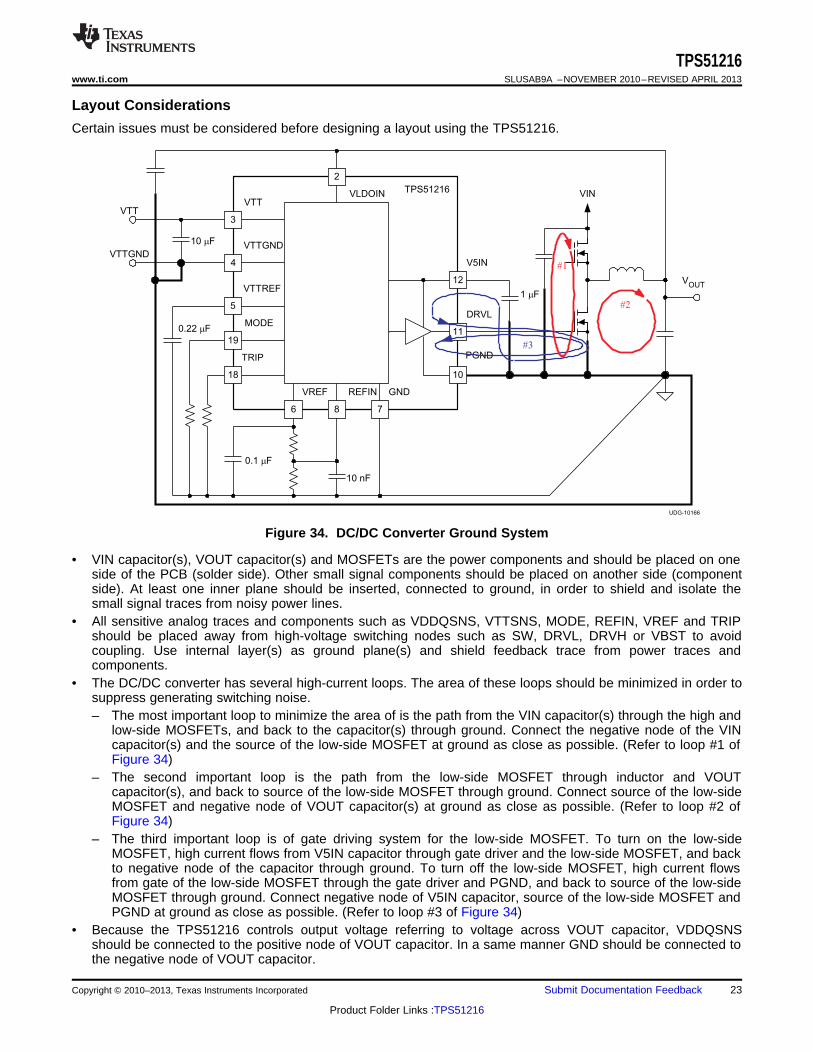
Layout Considerations
Certain issues must be considered before designing a layout using the TPS51216.
Figure 34. DC/DC Converter Ground System
• VIN capacitor(s), VOUT capacitor(s) and MOSFETs are the power components and should be placed on oneside of the PCB (solder side). Other small signal components should be placed on another side (componentside). At least one inner plane should be inserted, connected to ground, in order to shield and isolate thesmall signal traces from noisy power lines.
• All sensitive analog traces and components such as VDDQSNS, VTTSNS, MODE, REFIN, VREF and TRIPshould be placed away from high-voltage switching nodes such as SW, DRVL, DRVH or VBST to avoidcoupling. Use internal layer(s) as ground plane(s) and shield feedback trace from power traces andcomponents.
• The DC/DC converter has several high-current loops. The area of these loops should be minimized in order tosuppress generating switching noise.– The most important loop to minimize the area of is the path from the VIN capacitor(s) through the high and
low-side MOSFETs, and back to the capacitor(s) through ground. Connect the negative node of the VINcapacitor(s) and the source of the low-side MOSFET at ground as close as possible. (Refer to loop #1 ofFigure 34)
– The second important loop is the path from the low-side MOSFET through inductor and VOUTcapacitor(s), and back to source of the low-side MOSFET through ground. Connect source of the low-sideMOSFET and negative node of VOUT capacitor(s) at ground as close as possible. (Refer to loop #2 ofFigure 34)
– The third important loop is of gate driving system for the low-side MOSFET. To turn on the low-sideMOSFET, high current flows from V5IN capacitor through gate driver and the low-side MOSFET, and backto negative node of the capacitor through ground. To turn off the low-side MOSFET, high current flowsfrom gate of the low-side MOSFET through the gate driver and PGND, and back to source of the low-sideMOSFET through ground. Connect negative node of V5IN capacitor, source of the low-side MOSFET andPGND at ground as close as possible. (Refer to loop #3 of Figure 34)
• Because the TPS51216 controls output voltage referring to voltage across VOUT capacitor, VDDQSNSshould be connected to the positive node of VOUT capacitor. In a same manner GND should be connected tothe negative node of VOUT capacitor.
Copyright © 2010–2013, Texas Instruments Incorporated Submit Documentation Feedback 23
Product Folder Links :TPS51216
TPS51216SLUSAB9A –NOVEMBER 2010–REVISED APRIL 2013 www.ti.com
• Connect the overcurrent setting resistors from TRIP pin to ground and make the connections as close aspossible to the device. The trace from TRIP pin to resistor and from resistor to ground should avoid couplingto a high-voltage switching node.
• Connect the frequency and mode setting resistor from MODE pin to ground, and make the connections asclose as possible to the device. The trace from the MODE pin to the resistor and from the resistor to groundshould avoid coupling to a high-voltage switching node
• Connections from gate drivers to the respective gate of the high-side or the low-side MOSFET should be asshort as possible to reduce stray inductance. Use 0.65 mm (25 mils) or wider trace and via(s) of at least 0.5mm (20 mils) diameter along this trace.
• The PCB trace defined as SW node, which connects to the source of the switching MOSFET, the drain of therectifying MOSFET and the high-voltage side of the inductor, should be as short and wide as possible.
• VLDOIN should be connected to VDDQ output with short and wide traces. An input bypass capacitor shouldbe placed as close as possible to the pin with short and wide connections.
• The output capacitor for VTT should be placed close to the pin with a short and wide connection in order to avoid additional ESR and/or ESL of the trace.
• VTTSNS should be connected to the positive node of the VTT output capacitor(s) as a separate trace fromthe high-current power line and is strongly recommended to avoid additional ESR and/or ESL. If it is neededto sense the voltage at the point of the load, it is recommended to attach the output capacitor(s) at thatpoint. Also, it is recommended to minimize any additional ESR and/or ESL of ground trace between GND pinand the output capacitor(s).
• Consider adding a low pass filter (LPF) at VTTSNS in case the ESR of the VTT output capacitor(s) is largerthan 2 mΩ.
• VDDQSNS can be connected separately from VLDOIN. Remember that this sensing potential is the reference voltage of VTTREF. Avoid any noise generative lines.
• The negative node of the VTT output capacitor(s) and the VTTREF capacitor should be tied together byavoiding common impedance to high-current path of the VTT source/sink current.
• GND pin node represents the reference potential for VTTREF and VTT outputs. Connect GND to negativenodes of VTT capacitor(s), VTTREF capacitor and VDDQ capacitor(s) with care to avoid additional ESRand/or ESL. GND and PGND should be connected together at a single point.
• In order to effectively remove heat from the package, prepare the thermal land and solder to the package thermal pad. Wide trace of the component-side copper, connected to this thermal land, helps heatspreading. Numerous vias with a 0.3-mm diameter connected from the thermal land to the internal/solder-side ground plane(s) should be used to help dissipation.
CAUTION
Do NOT connect PGND pin directly to this thermal land underneath the package.
24 Submit Documentation Feedback Copyright © 2010–2013, Texas Instruments Incorporated
Product Folder Links :TPS51216
TPS51216www.ti.com SLUSAB9A –NOVEMBER 2010–REVISED APRIL 2013
REVISION HISTORY
Changes from Original (November 2010) to Revision A Page
• Added specifications to ABSOLUTE MAXIMUM RATINGS table. ....................................................................................... 2
• Added clarity to VTT and VTTREF section. ........................................................................................................................ 19
Copyright © 2010–2013, Texas Instruments Incorporated Submit Documentation Feedback 25
Product Folder Links :TPS51216
PACKAGE OPTION ADDENDUM
www.ti.com 15-Apr-2017
Addendum-Page 1
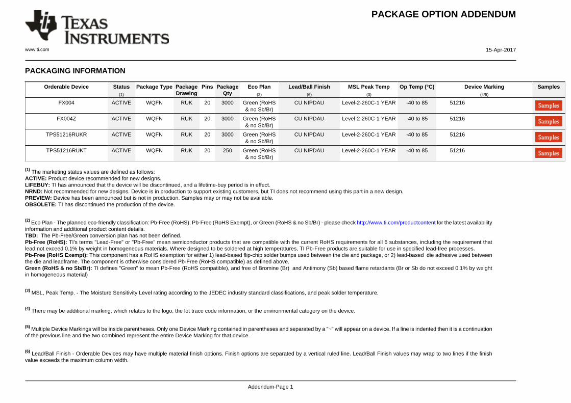
PACKAGING INFORMATION
Orderable Device Status(1)
Package Type PackageDrawing
Pins PackageQty
Eco Plan(2)
Lead/Ball Finish(6)
MSL Peak Temp(3)
Op Temp (°C) Device Marking(4/5)
Samples
FX004 ACTIVE WQFN RUK 20 3000 Green (RoHS& no Sb/Br)
CU NIPDAU Level-2-260C-1 YEAR -40 to 85 51216
FX004Z ACTIVE WQFN RUK 20 3000 Green (RoHS& no Sb/Br)
CU NIPDAU Level-2-260C-1 YEAR -40 to 85 51216
TPS51216RUKR ACTIVE WQFN RUK 20 3000 Green (RoHS& no Sb/Br)
CU NIPDAU Level-2-260C-1 YEAR -40 to 85 51216
TPS51216RUKT ACTIVE WQFN RUK 20 250 Green (RoHS& no Sb/Br)
CU NIPDAU Level-2-260C-1 YEAR -40 to 85 51216
(1) The marketing status values are defined as follows:ACTIVE: Product device recommended for new designs.LIFEBUY: TI has announced that the device will be discontinued, and a lifetime-buy period is in effect.NRND: Not recommended for new designs. Device is in production to support existing customers, but TI does not recommend using this part in a new design.PREVIEW: Device has been announced but is not in production. Samples may or may not be available.OBSOLETE: TI has discontinued the production of the device.
(2) Eco Plan - The planned eco-friendly classification: Pb-Free (RoHS), Pb-Free (RoHS Exempt), or Green (RoHS & no Sb/Br) - please check http://www.ti.com/productcontent for the latest availabilityinformation and additional product content details.TBD: The Pb-Free/Green conversion plan has not been defined.Pb-Free (RoHS): TI's terms "Lead-Free" or "Pb-Free" mean semiconductor products that are compatible with the current RoHS requirements for all 6 substances, including the requirement thatlead not exceed 0.1% by weight in homogeneous materials. Where designed to be soldered at high temperatures, TI Pb-Free products are suitable for use in specified lead-free processes.Pb-Free (RoHS Exempt): This component has a RoHS exemption for either 1) lead-based flip-chip solder bumps used between the die and package, or 2) lead-based die adhesive used betweenthe die and leadframe. The component is otherwise considered Pb-Free (RoHS compatible) as defined above.Green (RoHS & no Sb/Br): TI defines "Green" to mean Pb-Free (RoHS compatible), and free of Bromine (Br) and Antimony (Sb) based flame retardants (Br or Sb do not exceed 0.1% by weightin homogeneous material)
(3) MSL, Peak Temp. - The Moisture Sensitivity Level rating according to the JEDEC industry standard classifications, and peak solder temperature.
(4) There may be additional marking, which relates to the logo, the lot trace code information, or the environmental category on the device.
(5) Multiple Device Markings will be inside parentheses. Only one Device Marking contained in parentheses and separated by a "~" will appear on a device. If a line is indented then it is a continuationof the previous line and the two combined represent the entire Device Marking for that device.
(6) Lead/Ball Finish - Orderable Devices may have multiple material finish options. Finish options are separated by a vertical ruled line. Lead/Ball Finish values may wrap to two lines if the finishvalue exceeds the maximum column width.
PACKAGE OPTION ADDENDUM
www.ti.com 15-Apr-2017
Addendum-Page 2
Important Information and Disclaimer:The information provided on this page represents TI's knowledge and belief as of the date that it is provided. TI bases its knowledge and belief on informationprovided by third parties, and makes no representation or warranty as to the accuracy of such information. Efforts are underway to better integrate information from third parties. TI has taken andcontinues to take reasonable steps to provide representative and accurate information but may not have conducted destructive testing or chemical analysis on incoming materials and chemicals.TI and TI suppliers consider certain information to be proprietary, and thus CAS numbers and other limited information may not be available for release.
In no event shall TI's liability arising out of such information exceed the total purchase price of the TI part(s) at issue in this document sold by TI to Customer on an annual basis.
OTHER QUALIFIED VERSIONS OF TPS51216 :
• Enhanced Product: TPS51216-EP
NOTE: Qualified Version Definitions:
• Enhanced Product - Supports Defense, Aerospace and Medical Applications
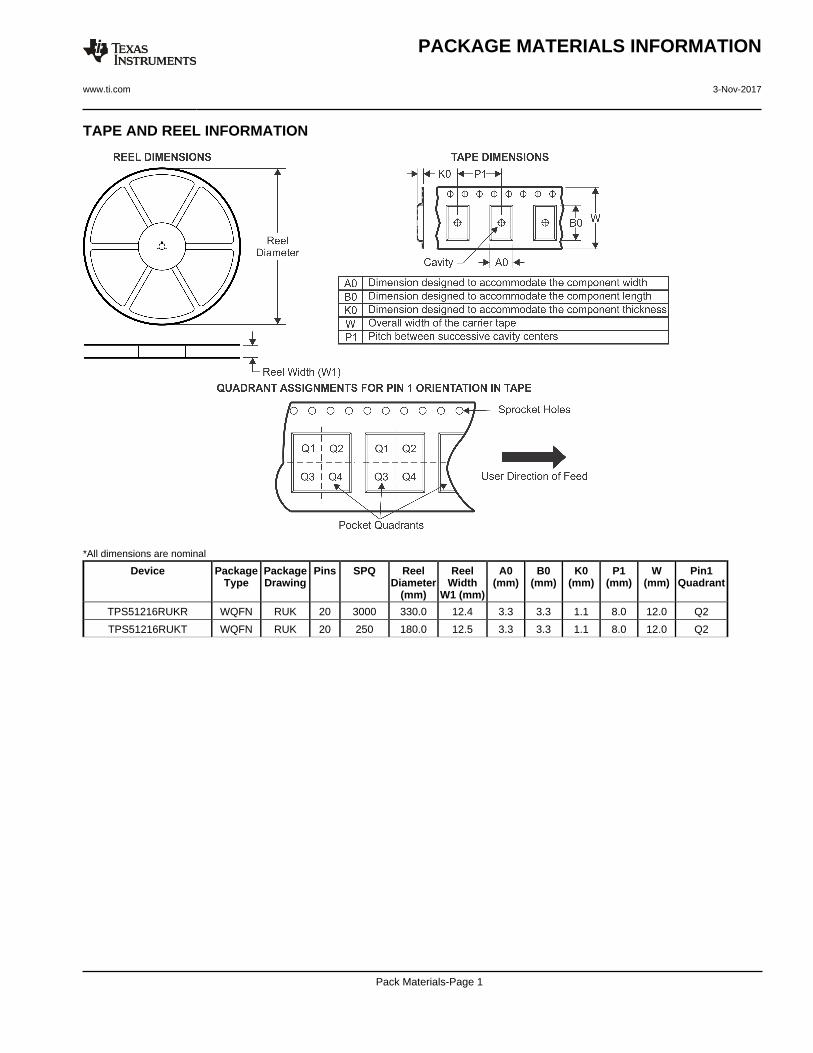
TAPE AND REEL INFORMATION
*All dimensions are nominal
Device PackageType
PackageDrawing
Pins SPQ ReelDiameter
(mm)
ReelWidth
W1 (mm)
A0(mm)
B0(mm)
K0(mm)
P1(mm)
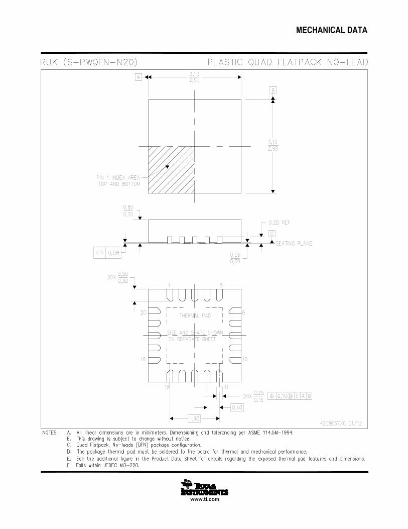
W(mm)
Pin1Quadrant
TPS51216RUKR WQFN RUK 20 3000 330.0 12.4 3.3 3.3 1.1 8.0 12.0 Q2
TPS51216RUKT WQFN RUK 20 250 180.0 12.5 3.3 3.3 1.1 8.0 12.0 Q2
PACKAGE MATERIALS INFORMATION
www.ti.com 3-Nov-2017
Pack Materials-Page 1
*All dimensions are nominal
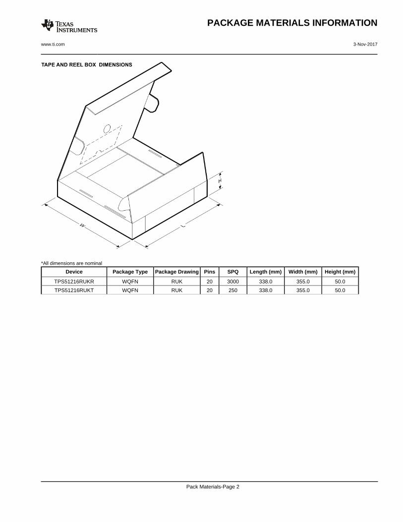
Device Package Type Package Drawing Pins SPQ Length (mm) Width (mm) Height (mm)
TPS51216RUKR WQFN RUK 20 3000 338.0 355.0 50.0
TPS51216RUKT WQFN RUK 20 250 338.0 355.0 50.0
PACKAGE MATERIALS INFORMATION
www.ti.com 3-Nov-2017
Pack Materials-Page 2

IMPORTANT NOTICE
Texas Instruments Incorporated (TI) reserves the right to make corrections, enhancements, improvements and other changes to itssemiconductor products and services per JESD46, latest issue, and to discontinue any product or service per JESD48, latest issue. Buyersshould obtain the latest relevant information before placing orders and should verify that such information is current and complete.TI’s published terms of sale for semiconductor products (http://www.ti.com/sc/docs/stdterms.htm) apply to the sale of packaged integratedcircuit products that TI has qualified and released to market. Additional terms may apply to the use or sale of other types of TI products andservices.Reproduction of significant portions of TI information in TI data sheets is permissible only if reproduction is without alteration and isaccompanied by all associated warranties, conditions, limitations, and notices. TI is not responsible or liable for such reproduceddocumentation. Information of third parties may be subject to additional restrictions. Resale of TI products or services with statementsdifferent from or beyond the parameters stated by TI for that product or service voids all express and any implied warranties for theassociated TI product or service and is an unfair and deceptive business practice. TI is not responsible or liable for any such statements.Buyers and others who are developing systems that incorporate TI products (collectively, “Designers”) understand and agree that Designersremain responsible for using their independent analysis, evaluation and judgment in designing their applications and that Designers havefull and exclusive responsibility to assure the safety of Designers' applications and compliance of their applications (and of all TI productsused in or for Designers’ applications) with all applicable regulations, laws and other applicable requirements. Designer represents that, withrespect to their applications, Designer has all the necessary expertise to create and implement safeguards that (1) anticipate dangerousconsequences of failures, (2) monitor failures and their consequences, and (3) lessen the likelihood of failures that might cause harm andtake appropriate actions. Designer agrees that prior to using or distributing any applications that include TI products, Designer willthoroughly test such applications and the functionality of such TI products as used in such applications.TI’s provision of technical, application or other design advice, quality characterization, reliability data or other services or information,including, but not limited to, reference designs and materials relating to evaluation modules, (collectively, “TI Resources”) are intended toassist designers who are developing applications that incorporate TI products; by downloading, accessing or using TI Resources in anyway, Designer (individually or, if Designer is acting on behalf of a company, Designer’s company) agrees to use any particular TI Resourcesolely for this purpose and subject to the terms of this Notice.TI’s provision of TI Resources does not expand or otherwise alter TI’s applicable published warranties or warranty disclaimers for TIproducts, and no additional obligations or liabilities arise from TI providing such TI Resources. TI reserves the right to make corrections,enhancements, improvements and other changes to its TI Resources. TI has not conducted any testing other than that specificallydescribed in the published documentation for a particular TI Resource.Designer is authorized to use, copy and modify any individual TI Resource only in connection with the development of applications thatinclude the TI product(s) identified in such TI Resource. NO OTHER LICENSE, EXPRESS OR IMPLIED, BY ESTOPPEL OR OTHERWISETO ANY OTHER TI INTELLECTUAL PROPERTY RIGHT, AND NO LICENSE TO ANY TECHNOLOGY OR INTELLECTUAL PROPERTYRIGHT OF TI OR ANY THIRD PARTY IS GRANTED HEREIN, including but not limited to any patent right, copyright, mask work right, orother intellectual property right relating to any combination, machine, or process in which TI products or services are used. Informationregarding or referencing third-party products or services does not constitute a license to use such products or services, or a warranty orendorsement thereof. Use of TI Resources may require a license from a third party under the patents or other intellectual property of thethird party, or a license from TI under the patents or other intellectual property of TI.TI RESOURCES ARE PROVIDED “AS IS” AND WITH ALL FAULTS. TI DISCLAIMS ALL OTHER WARRANTIES ORREPRESENTATIONS, EXPRESS OR IMPLIED, REGARDING RESOURCES OR USE THEREOF, INCLUDING BUT NOT LIMITED TOACCURACY OR COMPLETENESS, TITLE, ANY EPIDEMIC FAILURE WARRANTY AND ANY IMPLIED WARRANTIES OFMERCHANTABILITY, FITNESS FOR A PARTICULAR PURPOSE, AND NON-INFRINGEMENT OF ANY THIRD PARTY INTELLECTUALPROPERTY RIGHTS. TI SHALL NOT BE LIABLE FOR AND SHALL NOT DEFEND OR INDEMNIFY DESIGNER AGAINST ANY CLAIM,INCLUDING BUT NOT LIMITED TO ANY INFRINGEMENT CLAIM THAT RELATES TO OR IS BASED ON ANY COMBINATION OFPRODUCTS EVEN IF DESCRIBED IN TI RESOURCES OR OTHERWISE. IN NO EVENT SHALL TI BE LIABLE FOR ANY ACTUAL,DIRECT, SPECIAL, COLLATERAL, INDIRECT, PUNITIVE, INCIDENTAL, CONSEQUENTIAL OR EXEMPLARY DAMAGES INCONNECTION WITH OR ARISING OUT OF TI RESOURCES OR USE THEREOF, AND REGARDLESS OF WHETHER TI HAS BEENADVISED OF THE POSSIBILITY OF SUCH DAMAGES.Unless TI has explicitly designated an individual product as meeting the requirements of a particular industry standard (e.g., ISO/TS 16949and ISO 26262), TI is not responsible for any failure to meet such industry standard requirements.Where TI specifically promotes products as facilitating functional safety or as compliant with industry functional safety standards, suchproducts are intended to help enable customers to design and create their own applications that meet applicable functional safety standardsand requirements. Using products in an application does not by itself establish any safety features in the application. Designers mustensure compliance with safety-related requirements and standards applicable to their applications. Designer may not use any TI products inlife-critical medical equipment unless authorized officers of the parties have executed a special contract specifically governing such use.Life-critical medical equipment is medical equipment where failure of such equipment would cause serious bodily injury or death (e.g., lifesupport, pacemakers, defibrillators, heart pumps, neurostimulators, and implantables). Such equipment includes, without limitation, allmedical devices identified by the U.S. Food and Drug Administration as Class III devices and equivalent classifications outside the U.S.TI may expressly designate certain products as completing a particular qualification (e.g., Q100, Military Grade, or Enhanced Product).Designers agree that it has the necessary expertise to select the product with the appropriate qualification designation for their applicationsand that proper product selection is at Designers’ own risk. Designers are solely responsible for compliance with all legal and regulatoryrequirements in connection with such selection.Designer will fully indemnify TI and its representatives against any damages, costs, losses, and/or liabilities arising out of Designer’s non-compliance with the terms and provisions of this Notice.
Mailing Address: Texas Instruments, Post Office Box 655303, Dallas, Texas 75265Copyright © 2017, Texas Instruments Incorporated