ibis ebd for ddr2/ddr3 module board · ebd provides a secure and interoperable way for ddr2/3...
TRANSCRIPT

Copyright © 2006-2009 IO Methodology Inc.
TMTM
IBIS EBD for DDR2/DDR3 Module Board
Lance Wang([email protected])
IBIS Summit DesignCon 2009February 5th, 2009
Copyright © 2006-2009 IO Methodology Inc.
Outline
IBIS EBD
DDR2/3 Topology Structures
Challenges and Techniques for EBD
Simulation Results using between board and EBD
Conclusions

Copyright © 2006-2009 IO Methodology Inc.
IBIS EBD
A "board level component" is the generic term to be used to describe a printed circuit board (PCB) or substrate which can contain components or even other boards, and which can connect to another board through a set of user visible pins.
A "board level component" is the generic term to be used to describe a printed circuit board (PCB) or substrate which can contain components or even other boards, and which can connect to another board through a set of user visible pins.
Copyright © 2006-2009 IO Methodology Inc.
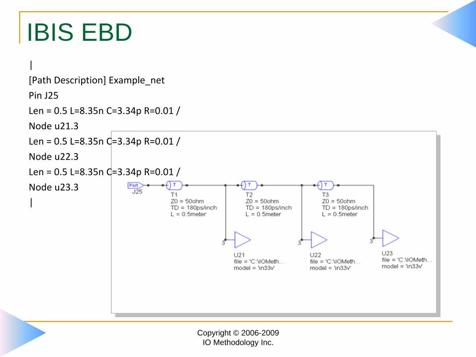
IBIS EBD |
[Path Description] Example_net
Pin J25
Len = 0.5 L=8.35n C=3.34p R=0.01 /
Node u21.3
Len = 0.5 L=8.35n C=3.34p R=0.01 /
Node u22.3
Len = 0.5 L=8.35n C=3.34p R=0.01 /
Node u23.3 |

Copyright © 2006-2009 IO Methodology Inc.
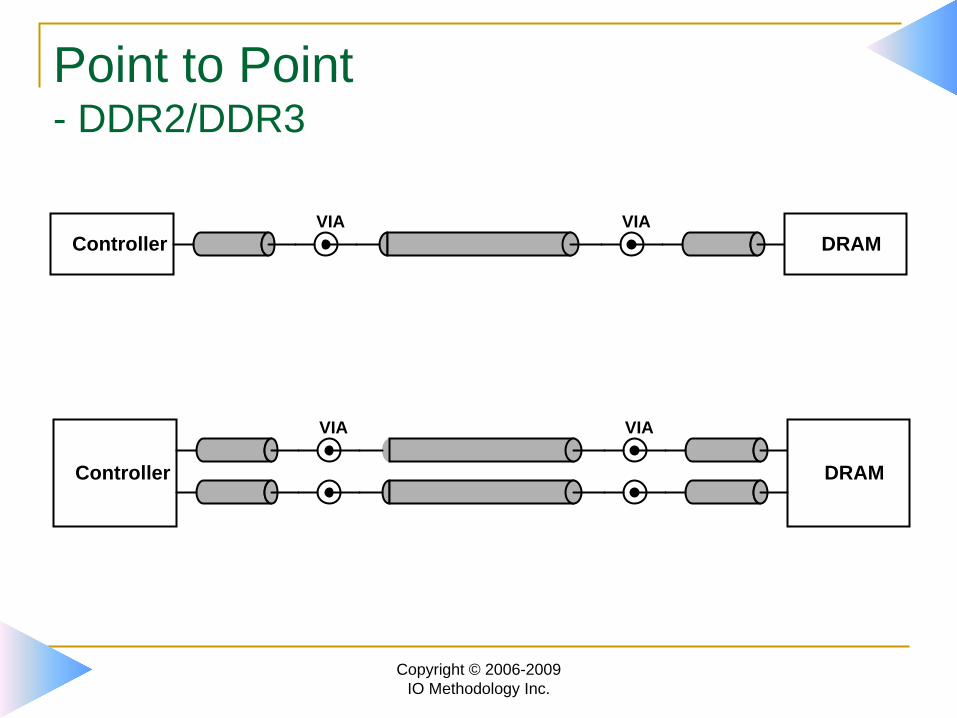
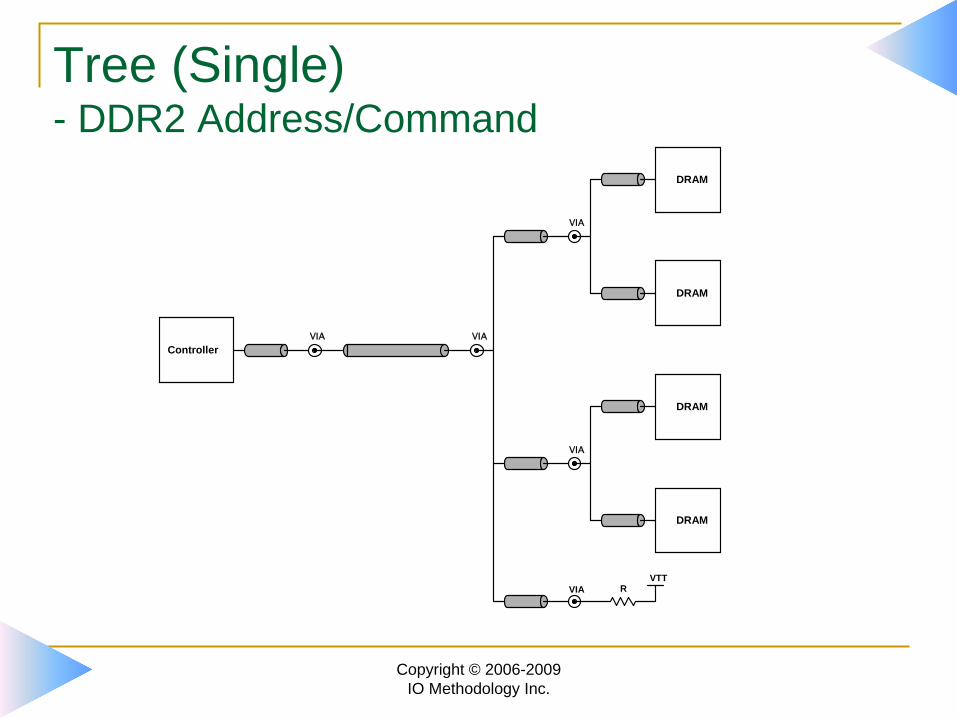
DDR2/3 Topology Structure
Point to Point
Tree
Fly-by
Copyright © 2006-2009 IO Methodology Inc.
Point to Point - DDR2/DDR3
ControllerVIA VIA
DRAM
Controller
VIA VIA
DRAM
Copyright © 2006-2009 IO Methodology Inc.
Tree (Single) - DDR2 Address/Command
DRAM
DRAM
DRAM
DRAM
ControllerVIA VIA
VIA
VIA
VIA RVTT

Copyright © 2006-2009 IO Methodology Inc.
Tree (Differential) - DDR2 Clock
DRAM
DRAM
DRAM
DRAM
Controller
VIA
VIA
VIA
VIA R
VIA
VIA
VIA
VIA

Copyright © 2006-2009 IO Methodology Inc.
Hybrid Tree - DDR2
DRAM
DRAM
DRAM
DRAM
ControllerVIA
VIA
VIA
VIA R VTT
VIA
VIA

Copyright © 2006-2009 IO Methodology Inc.
Fly-by (Daisy Chain) - DDR3 Address/Command
DRAM
DRAM
DRAM
DRAM
ControllerVIA
VIA
VIA
VIA R VTT
VIA
VIA

Copyright © 2006-2009 IO Methodology Inc.
Fly-by - DDR3 Clock
VDD
Cap2
Cap1
Dram Dram Dram Dram
Dram Dram Dram Dram
Controller
R
Copyright © 2006-2009 IO Methodology Inc.
Challenges and Techniques for EBD
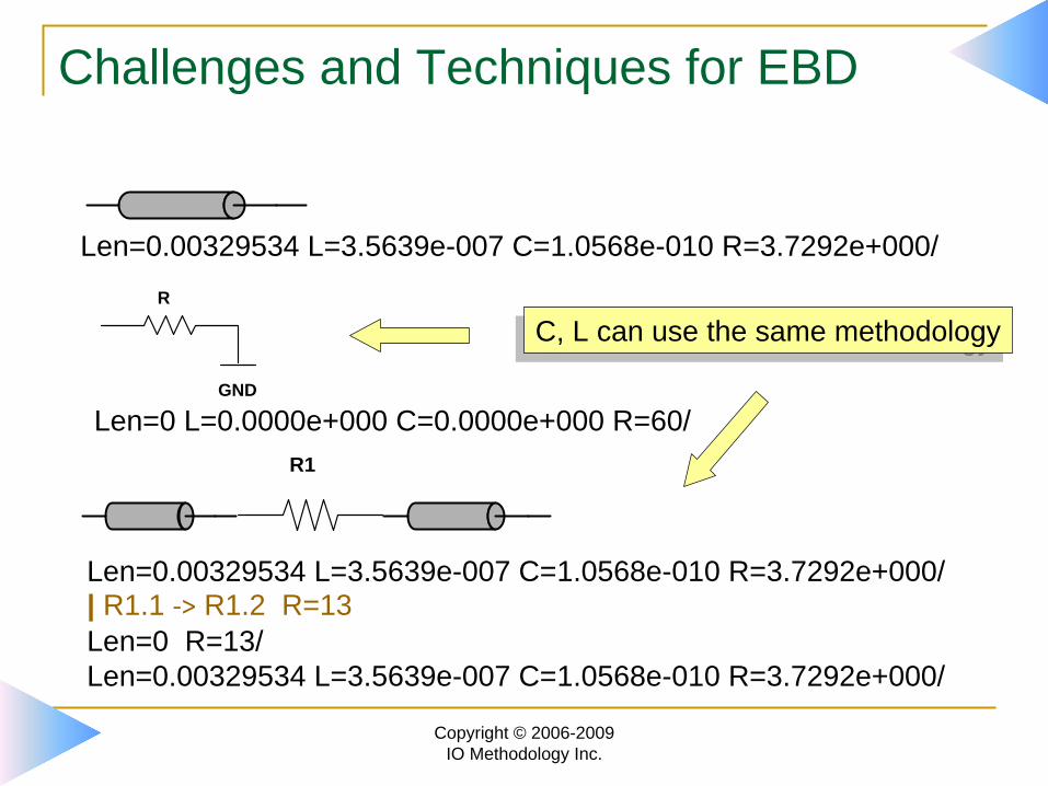
Len=0.00329534 L=3.5639e-007 C=1.0568e-010 R=3.7292e+000/ R
GND
Len=0 L=0.0000e+000 C=0.0000e+000 R=60/
C, L can use the same methodologyC, L can use the same methodology
R1
Len=0.00329534 L=3.5639e-007 C=1.0568e-010 R=3.7292e+000/ | R1.1 ‐>
R1.2 R=13Len=0 R=13/Len=0.00329534 L=3.5639e-007 C=1.0568e-010 R=3.7292e+000/
Copyright © 2006-2009 IO Methodology Inc.
[Model] series_r39Model_type Series| typ min maxC_comp 0 NA NA[Pullup Reference] 0 NA NA[Pulldown Reference] 0 NA NA[POWER Clamp Reference] 0 NA NA[GND Clamp Reference] 0 NA NA| variable typ min max[R Series] 39 NA NA
[Model] series_r39Model_type Series| typ min maxC_comp 0 NA NA[Pullup Reference] 0 NA NA[Pulldown Reference] 0 NA NA[POWER Clamp Reference] 0 NA NA[GND Clamp Reference] 0 NA NA| variable typ min max[R Series] 39 NA NA
[Model] P_VTTModel_type Terminator| typ min maxC_comp 0 NA NA[Pullup Reference] 0.9 NA NA[Pulldown Reference] 0 NA NA[POWER Clamp Reference] 0.9 NA NA[GND Clamp Reference] 0 NA NA| variable typ min max[Rpower] 0 NA NA
[Model] P_VTTModel_type Terminator| typ min maxC_comp 0 NA NA[Pullup Reference] 0.9 NA NA[Pulldown Reference] 0 NA NA[POWER Clamp Reference] 0.9 NA NA[GND Clamp Reference] 0 NA NA| variable typ min max[Rpower] 0 NA NA
Challenges and Techniques for EBD
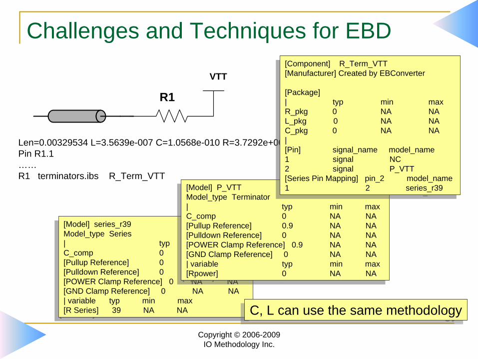
Len=0.00329534 L=3.5639e-007 C=1.0568e-010 R=3.7292e+000/Pin R1.1……R1 terminators.ibs R_Term_VTT
R1
VTT[Component] R_Term_VTT[Manufacturer] Created by EBConverter
[Package]| typ min maxR_pkg 0 NA NAL_pkg 0 NA NAC_pkg 0 NA NA| [Pin] signal_name model_name1 signal NC2 signal P_VTT[Series Pin Mapping] pin_2 model_name1 2 series_r39
[Component] R_Term_VTT[Manufacturer] Created by EBConverter
[Package]| typ min maxR_pkg 0 NA NAL_pkg 0 NA NAC_pkg 0 NA NA|[Pin] signal_name model_name1 signal NC2 signal P_VTT[Series Pin Mapping] pin_2 model_name1 2 series_r39
C, L can use the same methodologyC, L can use the same methodology

Copyright © 2006-2009 IO Methodology Inc.
Challenges and Techniques for EBD
RN10.2, 7
! Net CLK_PPin 170...... Len=0.00329534 L=3.5639e-007 C=1.0568e-010 R=3.7292e+000/ | RN10.2 ‐> RN10.7 R=13Len=0 R=13/| Net: CLK_NLen=0.00182395 L=3.5639e-007 C=1.0568e-010 R=3.7292e+000/......Pin 171
! Net CLK_PPin 170...... Len=0.00329534 L=3.5639e-007 C=1.0568e-010 R=3.7292e+000/ | RN10.2 ‐> RN10.7 R=13Len=0 R=13/| Net: CLK_NLen=0.00182395 L=3.5639e-007 C=1.0568e-010 R=3.7292e+000/......Pin 171
C, L can use the same methodologyC, L can use the same methodology
Make sure to put both nets in the
same [Path Description]
BIRD 111.1 describes another method
Copyright © 2006-2009 IO Methodology Inc.
Simulation Results using between board and EBD
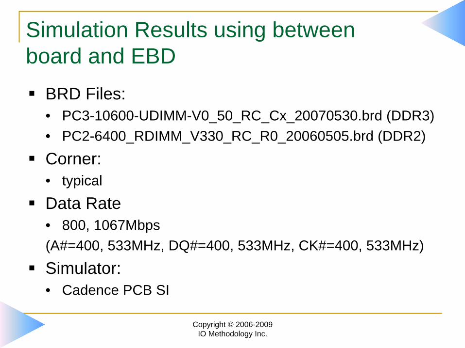
BRD Files:• PC3-10600-UDIMM-V0_50_RC_Cx_20070530.brd (DDR3)• PC2-6400_RDIMM_V330_RC_R0_20060505.brd (DDR2)
Corner:• typical
Data Rate• 800, 1067Mbps (A#=400, 533MHz, DQ#=400, 533MHz, CK#=400, 533MHz)
Simulator:• Cadence PCB SI

Copyright © 2006-2009 IO Methodology Inc.
Net: DQ# @ U1 Timing:0.002ps @750mv DPI: 0.00% DAI: 0.00%
PERFECT MATCHPERFECT MATCH
ControllerVIA VIA
DRAM
Copyright © 2006-2009 IO Methodology Inc.
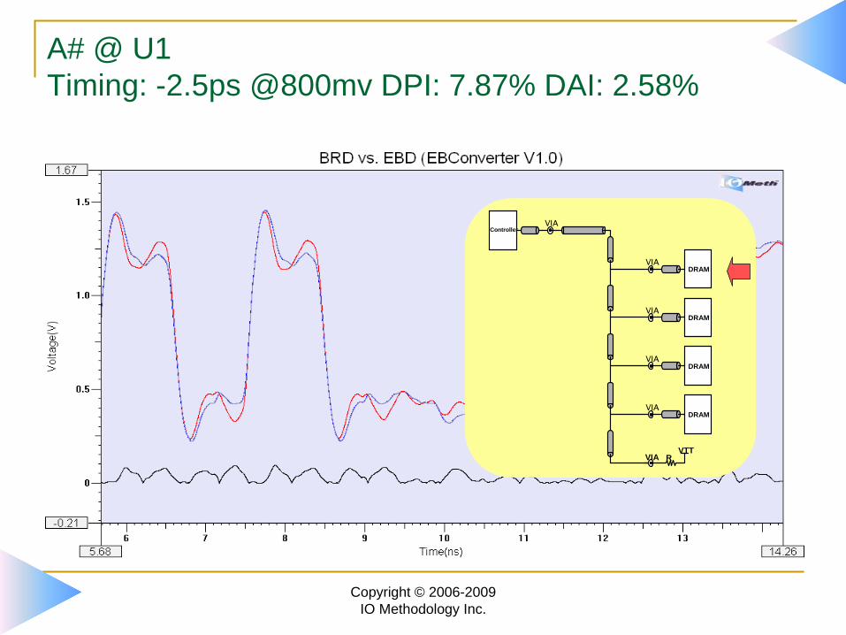
A# @ U1 Timing: -2.5ps @800mv DPI: 7.87% DAI: 2.58%
DRAM
DRAM
DRAM
DRAM
ControllerVIA
VIA
VIA
VIA R VTT
VIA
VIA

Copyright © 2006-2009 IO Methodology Inc.
A# @ U4 Timing:51ps @800mv DPI: 2.67% DAI: 0.86%
DRAM
DRAM
DRAM
DRAM
ControllerVIA
VIA
VIA
VIA R VTT
VIA
VIA

Copyright © 2006-2009 IO Methodology Inc.
CK#/CK#_ @ U1 Timing:66ps @0v DPI: 26.63% DAI: 5.60%
VDD
Cap2
Cap1
Dram Dram Dram Dram
Controller
R

Copyright © 2006-2009 IO Methodology Inc.
CK#/CK#_ @ U4 Timing:63ps @0v DPI: 9.57% DAI: 1.86%
VDD
Cap2
Cap1
Dram Dram Dram Dram
Controller
R

Copyright © 2006-2009 IO Methodology Inc.
CK#/CK#_ @ U1 (Diff Coupled) Timing:101ps @0v DPI: 27.35% DAI: 6.23%
VDD
Cap2
Cap1
Dram Dram Dram Dram
Controller
R

Copyright © 2006-2009 IO Methodology Inc.
Conclusions
EBD provides a secure and interoperable way for DDR2/3 modules in the high-speed memory market
It is accepted by the most of EDA software now
Needs to be careful to model EBD using correct method
Good for point-to-point, Tree structure topologies
Good Signal Quality for Fly-By structure, not good for Timing (Single-end)
Acceptable Signal Quality for Fly-By structure, not good for Timing (Differential)• Signal Quality might also effected by timing on reflections
Two new elements needs to be added:• Delay/Lossy Element
Adding frequency-dependent Rs, Gd elements into RLC (easy to convert from W-element like lossy transmission line syntax)
• Coupling Element
Mutual Capacitance

TMTM
The High‐Speed Design Utility Tool and Service Providerwww.iometh.com
The High‐Speed Design Utility Tool and Service Providerwww.iometh.com