using high-performance ddr, ddr2, ddr3 sdram with sopc builder · using high-performance ddr, ddr2,...
TRANSCRIPT
Altera Corporation AN-517-1.0
March 2008, version 1.0
Using High-PerformanceDDR, DDR2, and DDR3
SDRAM With SOPC Builder
Application Note 517Introduction The Altera® DDR, DDR2, and DDR3 SDRAM High-Performance Controller MegaCore® functions version 7.1 and later support SOPC Builder, enabling you to instantiate a DDR, DDR2, or DDR3 SDRAM high-performance controller in an SOPC Builder system. This application note discusses the following topics:
■ Consider SOPC Builder system interconnect fabric and performance implications:● Full- or half-rate SDRAM high-performance controller● System and component clock selection and clock crossing
bridges● Burst reads and writes● Latency and how to optimize read or write addressing
■ Implement a DDR2 SDRAM High Performance Controller in SOPC Builder
■ Incorporate a Nios® II Processor and other peripherals■ Compile the design and generate the programming file■ Download the design to a development board and run sample code
on your design to test read and write transactions
f For more information on functional simulation of an SOPC Builder system, refer to AN 351: Simulating Nios II Embedded Processor Designs.
f For more information on using legacy DDR or DDR2 SDRAM Controller MegaCore functions with SOPC Builder, see AN 398: Using DDR/DDR2 SDRAM with SOPC Builder.
f For more information about the DDR, DDR2, and DDR3 SDRAM High Performance Controllers, refer to the DDR and DDR2 SDRAM High-Performance Controller User Guide and the DDR3 SDRAM High-Performance Controller User Guide.
SOPC Builder System Considerations
Always consider the following caveats and limitations when integrating a DDR, DDR2, or DDR3 SDRAM high-performance controller in SOPC Builder.
Full- or Half-Rate SDRAM High-Performance Controller
Full- or half-rate SDRAM high-performance controllers have the following definitions:
6.1 1 Preliminary
Using High-Performance DDR, DDR2, and DDR3 SDRAM With SOPC Builder
■ Full-rate controllers present data to the local interface at twice the width of the actual SDRAM interface at the full SDRAM clock rate.
■ Half-rate controllers present data to the local interface at four times the width of the actual SDRAM interface at half the SDRAM clock rate.
Implementing the SDRAM high-performance controllers in half-rate mode gives the highest possible SDRAM clock frequency while allowing the more complex core logic to operate at half this frequency. You can simplify the complexity of your design by permitting your Nios II processor to run at the slower, half-rate memory speed while still achieving the required SDRAM bandwidth per I/O pin.
However, where possible it is generally more optimal to configure the controller in full-rate mode with the core operating at the same clock frequency as your SOPC Builder system.
Full-Rate Versus Half-Rate Command Operation
Comamnds can be slower using a half-rate controller. For example, a DDR SDRAM device can have a number of banks open at once. Each bank has a currently selected row. Changing the column within the selected row of an open bank requires no additional bank management commands to be issued. Changing the row in an active bank, or changing the bank both incur a protocol penalty that requires the precharge (PCH) command closes the active row or bank, and the active (ACT) command then opens (or activates) the new row or bank combination.
The duration of this penalty is a function of the controller clock frequency, the memory clock frequency, and the memory device characteristics. Calculating the impact of a change of memory and controller configuration on a given system is not a trivial task, as it depends on the nature of the accesses that are performed.
In this example each command takes a single clock cycle in a full-rate controller, but two clock cycles in a half-rate controller. The bank is not available for the subsequent ACT command until (tRP) after the PCH. So the issuing of commands can be slower using a half-rate controller, even if the respective memory timing parameters remain the same.
Time-Specified Memory Parameters
For a half-rate SDRAM high-performance controller, the control circuitry is clocked at half rate and so control operations are slower than in full-rate mode. However, the memory's clock frequency and physical properties are not affected.
2 6.1 Altera CorporationPreliminary
SOPC Builder System Considerations
When you use half-rate mode, any time-specified memory parameters in the controller are modified.
For example, if:
tRCDmin = 20 ns
For a 133-MHz controller:
tCK = 7.5 ns
20/7.5 = 2.666 rounded up to 3 clock cycles (22.5ns).
For a half-rate 66-MHz controller:
tCK = 15 ns
20/15 = 1.33 rounded up to 2 clock cycles (30ns).
Thus bank and row changes are slower in half-rate mode, but are not twice as slow. The easiest way to measure this effect for your chosen memory device and interface clock speed is to simulate both half-rate and full-rate designs and record the increased latency when switching rows. Typically a full-rate controller is around 14% more efficient when switching rows within a bank. As a half-rate controller has less read latency and if the masters in your system do not cause bank switching to occur often, the half-rate controller still gives higher performance. In SOPC Builder, you can alter arbitration shares to prevent masters from switching memory banks, thus creating a more optimal system.
Clock Selection and Clock Crossing Bridges
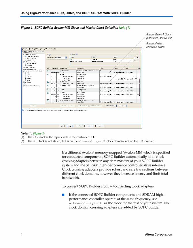
Ideally every component in the SOPC Builder system should be clocked using the same clock, to prevent SOPC Builder automatically adding clock domain crossing logic, which adds latency. The SDRAM high-performance controllers already include a PLL, so you should set the SOPC Builder system clock to altmemddr.sysclk, which is the clock the controller and local interface logic use. SOPC Builder only shows the input clock to the controller PLL, not the interface clock, see Figure 1.
Altera Corporation 6.1 3Preliminary
Using High-Performance DDR, DDR2, and DDR3 SDRAM With SOPC Builder
Figure 1. SOPC Builder Avalon-MM Slave and Master Clock Selection Note (1)
Notes to Figure 1:(1) The clk clock is the input clock to the controller PLL.(2) The s1 clock is not stated, but is on the altmemddr.sysclk clock domain, not on the clk domain.
If a different Avalon® memory-mapped (Avalon-MM) clock is specified for connected components, SOPC Builder automatically adds clock crossing adapters between any data masters of your SOPC Builder system and the SDRAM high-performance controller slave interface. Clock crossing adapters provide robust and safe transactions between different clock domains, however they increase latency and limit total bandwidth.
To prevent SOPC Builder from auto-inserting clock adapters:
■ If the connected SOPC Builder components and SDRAM high-performance controller operate at the same frequency, use altmemddr.sysclk as the clock for the rest of your system. No clock domain crossing adapters are added by SOPC Builder.
Avalon Slave s1 Clock(not stated, see Note 2)
Avalon Masterand Slave Clocks
4 6.1 Altera CorporationPreliminary
SOPC Builder System Considerations
■ If connected SOPC Builder components and SDRAM high-performance controller operate at different frequencies, manually insert an Avalon-MM clock crossing bridge between the SDRAM high-performance controller and the other SOPC Builder components.
To use the Avalon-MM clock crossing bridge, set its slave clock to your SOPC Builder system clock, and its master clock to altmemddr.sysclk. This component uses a FIFO for decoupling clock domains and is much more bandwidth efficient than the auto-inserted bridge. Size and structure of the bridge can be parameterized to implement a solution that is better optimized with lower latency.
f For more information, refer to the Clock Domain Crossing section in the System Interconnect Fabric for Memory-Mapped Interfaces chapter and the Avalon Memory-Mapped Bridges chapter in the Quartus II Handbook.
1 The Avalon-MM clock crossing bridge also works when you are using two different clocks at the same frequency but with different phases.
Use the Avalon-MM clock crossing bridge to allow a full-rate controller to connect to a half-rate SOPC builder design. The memory controller can still operate at a full-rate twice the Nios II frequency. So the memory interface commands operate at the faster rate. Figure 2 shows a clock crossing bridge example.
Altera Corporation 6.1 5Preliminary
Using High-Performance DDR, DDR2, and DDR3 SDRAM With SOPC Builder
Figure 2. Clock Crossing Bridge
Burst Reads and Writes
Table 1 shows the burst length support for each type of SDRAM high-performance controller.
Burst reads and writes differ in the following ways:
■ In half-rate mode, the Avalon-MM slave interface is four times the width of the SDRAM device. Hence four transactions are performed on the SDRAM for every single Avalon-MM transaction. Avalon-MM burst requests on the local side serve no purpose as the memory interface is already using the maximum supported memory burst size for every single Avalon-MM transaction.
Table 1. Burst Length Support
Memory Type Full-Rate Mode Half-Rate Mode
DDR3 — 8
DDR2 4 4
DDR 2 or 4 4
M M
M
S
Nios IIProcessor
S
JTAGUART
M
M M
DMAController
S
On-ChipMemory
Arbiter Arbiter
S
PIO
150 MHz
75 MHz
Avalon-MM Slave Interface
Avalon-MM Master Interface
S
Clock-CrossingBridge
S
SDRAMController
6 6.1 Altera CorporationPreliminary
SOPC Builder System Considerations
■ In full-rate mode, you can use Avalon-MM bursts of one or two with the SDRAM high-performance controller, as each Avalon-MM transaction results in only two SDRAM transactions. So two Avalon-MM burst transactions may be combined to support the four supported on the SDRAM high-performance controller.
1 When a burst capable master supports larger burst lengths than the slave, SOPC Builder automatically places a burst length adapter into the path.
To obtain performance advantages, ensure that the data widths of master and slave pairs are matched in SOPC Builder. Whenever a master port is connected to a slave port of a different width, SOPC Builder automatically inserts adapter logic to convert between the different data widths.
Ideally, the data size of an Avalon-MM interface is 32 bits for a Nios II processor:
■ For a full-rate SDRAM high-performance controller, the double-data rate stage doubles the data width, thus a 16-bit external memory width is best.
■ For a half-rate SDRAM high-performance controller, the double-data rate and half-rate stages both double the data width, thus an 8-bit external memory width is best.
Ideally, match the following data cache line sizes to the memory controller burst length:
■ 4-byte line = bursts of 1 (32-bit word)■ 16-byte line = bursts of 4■ 32-byte line = bursts of 8
You can set the data bus arbitration priority to avoid using the burst signal.
Multimasters
To achieve best throughput and latency of the SDRAM, you should connect the controller to the smallest number of masters and share those masters with the smallest number of slaves. Fewer connections reduce the complexity of the SOPC Builder auto-inserted data multiplexers and increase the fMAX of the Avalon-MM interface.
1 If the Avalon-MM interface fMAX becomes the limiting factor, insert pipeline bridges to increase fMAX the (at the expense of latency).
Altera Corporation 6.1 7Preliminary
Using High-Performance DDR, DDR2, and DDR3 SDRAM With SOPC Builder
Master and slave pairs are locked for the whole duration of a burst—no other master is granted access to the slave target of a burst until the burst is completed. You should isolate critical memory connections from the rest of the system.
One master may lock an SDRAM high-performance controller until a write burst is completed, which may take several cycles of time, during which the SDRAM high-performance controller cannot accept any other request. The write burst command is complete when all burst data is passed to the SDRAM high-performance controller. For a read burst, the controller quickly transfers back the whole burst at full bandwidth and becomes immediately available for new requests.
Read and Write Addressing and Latency
Systems with deterministic access patterns can minimize the number of bank and row changes. For example, by suitably arranging the memory map. In systems with more random access patterns (often typical in embedded SOPC Builder-type systems), minimizing bank and row changes is more difficult and the increased latency (by constantly changing the row in an active bank, or changing the bank) has a greater effect. Non-optimal cache implementations can waste cycles with half-rate controllers.
You should always consider the following actions:
■ Match controller Avalon-MM interface width to Avalon-MM master interface width.
■ Minimize non-sequential addressing to reduce row addressing time.■ Match the Nios II cache line size to memory burst length.■ Set arbitration priorities correctly.■ Insert bridges to increase fMAX at the expense of latency.■ Minimize multimaster designs where arbitration stalls may take
place.1 In multi-mastering designs, the memory is not available to
all masters concurrently.
Setting the arbitration priorities correctly prevents unnecessary memory accesses. For example, always set the Nios II instruction master arbitration priority to eight, because it always tries to access eight sequential addresses. Set the data master arbitration priorities depending on the cache line size; do not leave the arbitration priority value as default.
8 6.1 Altera CorporationPreliminary
DDR2 SDRAM High-Performance Controller with SOPC Builder Walkthrough
DDR2 SDRAM High-Performance Controller with SOPC Builder Walkthrough
This application note assumes that you are familiar with the Quartus® II software and SOPC Builder. To use this application note, ensure you have the following software on your computer:
■ Quartus® II version 7.2■ ModelSim-Altera 6.1g or higher ■ DDR2 SDRAM High-Performance Controller v7.2■ Nios II Embedded Design Suite (EDS) version 7.2
The design is targeted to the Cyclone® III FPGA Development Kit. You can target other supported device families or development kits.
f For more information on the Cyclone III FPGA Development Kit, refer to www.altera.com/products/devkits/altera/kit-cyc3.html.
Create Your Example Project
This section shows you how to create a new Quartus II project and an SOPC Builder system.
Create a New Quartus II Project
In the Quartus II software, create a new project with the New Project Wizard, ensure that the device type is set to Cyclone III, EP3C120F780C7.
1 Ensure that your project path does not include any spaces or extended characters.
Create the SOPC Builder System
To create an SOPC Builder system, follow these steps:
1. On the Tools menu click SOPC Builder.
2. In the Create New System dialog box, enter sopc_top for the System Name. In the Target HDL, select Verilog, then click OK.
3. On the System Contents tab expand Memories and Memory Controllers. Expand SDRAM. Select DDR2 SDRAM High Performance Controller and click Add. The DDR2 SDRAM high-performance controller wizard opens.
4. For the Speed Grade, select 7, to match the chosen device.
5. For the PLL reference clock frequency, enter 50 MHz, to match signal CLKIN50.
Altera Corporation 6.1 9Preliminary

Using High-Performance DDR, DDR2, and DDR3 SDRAM With SOPC Builder
6. For the Memory clock frequency, enter 150 MHz.
1 150 MHz is the maximum supported frequency for DDR2, SSTL-18 class I, in top and bottom I/O, in a C7 speed grade Cyclone III device.
7. For the Local interface clock frequency, select Half.
8. For the Memory vendor, select Micron.
9. For the Memory format, select Discrete Device.
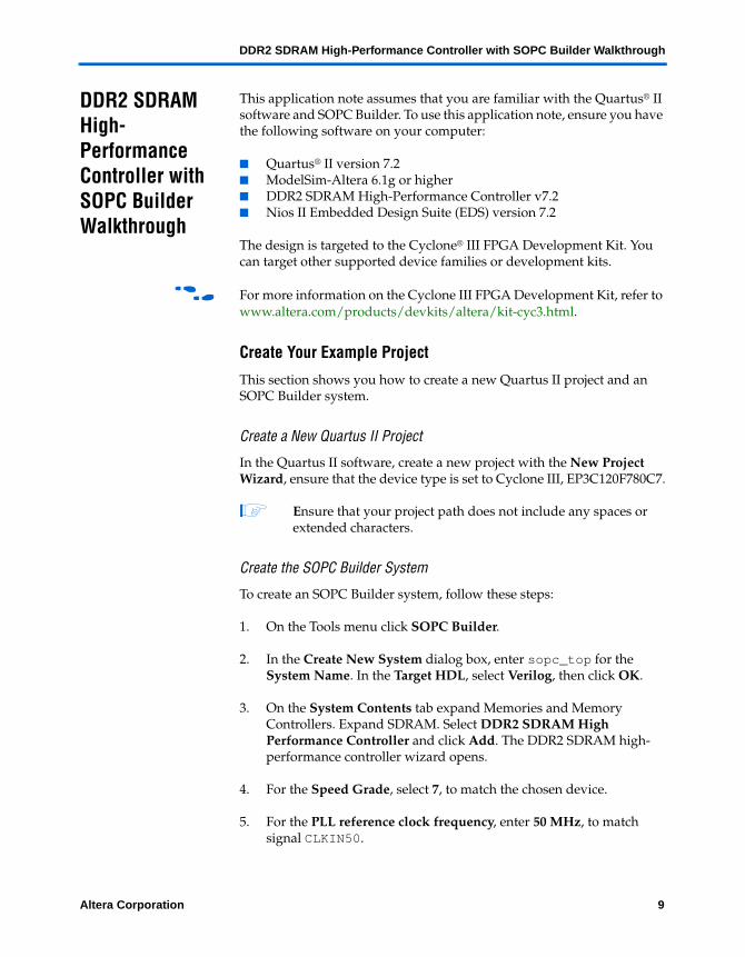
10. For the Memory Presets, select Micron MT47H32M16CC-3 x4 + MT47H32M8BP-3 x1 (see Figure 3).
1 This memory preset has been included by Altera in the DDR2 SDRAM high-performance controller as it matches the exact configuration that both the Cyclone III development board and the Stratix II GX PCIe Development Kit use.
10 6.1 Altera CorporationPreliminary
DDR2 SDRAM High-Performance Controller with SOPC Builder Walkthrough
Figure 3. Memory Settings
11. Click Modify parameters and ensure you change the following parameters:
● Output clock pairs from FPGA, select 1 pairs● Memory interface DQ width, select 8 bits, to give in an Avalon-
MM width of 32 bits, which is ideal to connect to a Nios II processor
● Memory drive strength setting, select Reduced (DQ are low load point-to-point connections)
Altera Corporation 6.1 11Preliminary
Using High-Performance DDR, DDR2, and DDR3 SDRAM With SOPC Builder
● Memory on-die termination (ODT) setting, select Disabled (discrete class I termination is already fitted to the development board)
● Memory CAS latency setting, select 3.0 cycles (this DDR2 SDRAM supports CAS = 3 for frequencies of 200 MHz or lower)
12. Click OK then click Finish in the DDR2 SDRAM high-performance controller wizard.
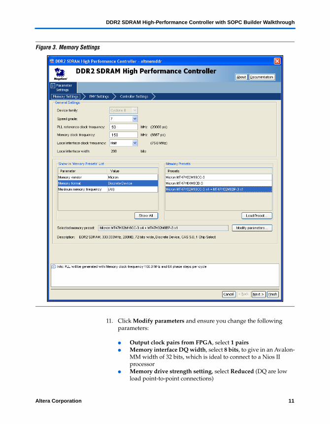
Figure 4. Preset Editor
Add SOPC Builder Components
To add components from the System Contents tab, follow these steps:
12 6.1 Altera CorporationPreliminary
DDR2 SDRAM High-Performance Controller with SOPC Builder Walkthrough
1. Expand On-Chip Memory and select On-Chip Memory, click Add. For Total memory size enter 64 KBytes. Click Finish.
2. Select On-Chip Memory again, click Add.
a. Set Total memory size to 4096 Bytes.
b. Select Finish.
c. Right click on this second on-chip memory, click Rename and type dma_read_memory and press Enter.
3. On the System menu, click Auto-Assign Base Addresses.
4. Select Nios II Processor and click Add.
a. Select Nios II/s.
b. For Reset Vector and Exception Vector select onchip_mem. If local on-chip memory holds the Nios II instruction code, less arbitration is required to the SDRAM interface resulting in a more optimal Avalon-MM structure.
c. Change Reset Vector Offset to 0x20 and Exception Vector Offset to 0x40.
c The controller performs memory interface calibration every time it is reset and in doing so writes to addresses 0x0 to 0x1f. If you want your memory contents to remain intact through a system reset, you should avoid using the memory addresses below 0x20. This step is not necessary, if you reload your SDRAM contents from flash every time you reset.
d. Click Finish.
5. Expand Interface Protocols and expand Serial, select JTAG UART and click Add.
a. For both the read and write FIFO, for the Buffer Depth (bytes) select 64 and for IRQ threshold enter 8.
b. Click Finish.
6. Expand Peripherals and expand Microcontroller Peripherals, select PIO (Parallel I/O), click Add.
a. For the Width enter 8 bits.
Altera Corporation 6.1 13Preliminary
Using High-Performance DDR, DDR2, and DDR3 SDRAM With SOPC Builder
b. For Direction select Output ports only.
c. Click Finish.
7. Expand Memories and Memory Controllers and expand DMA, select DMA Controller and click Add.
a. Turn on Enable burst transfers, for the Maximum burst size select 512 words.
b. Click the Advanced tab. Turn off doubleword and quadword on the Advanced tab.
c. Click Finish.
1 Do not to add a PLL component to your SOPC Builder design as the DDR2 SDRAM high-performance controller includes one.
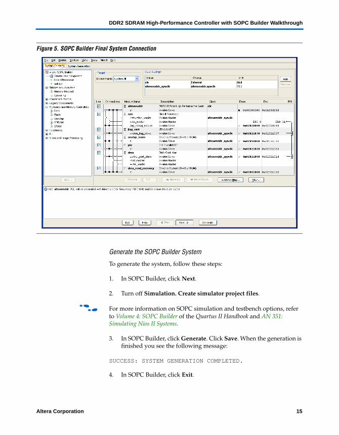
8. Set the bus links (see Figure 5).
a. Connect the DMA read_master and write_master to both the altmemddr and the dma_read_memory.
1 If there are warnings about overlapping addresses, on the System menu click Auto-Assign Base Addresses.
1 If there are warnings about overlapping IRQ, on the System menu click Auto-Assign IRQs.
b. Ensure that altmemddr is clocked on the external clock clk and that the frequency matches the external oscillator (50 MHz for the Cyclone III development board).
c. Ensure that all other modules are clocked on the altmemddr_sysclk, to avoid any unnecessary clock-domain crossing logic.
f For more information on SOPC Builder system interconnect fabric, refer to the System Interconnect Fabric for Memory-Mapped Interfaces chapter in the Quartus II Handbook.
14 6.1 Altera CorporationPreliminary
DDR2 SDRAM High-Performance Controller with SOPC Builder Walkthrough
Figure 5. SOPC Builder Final System Connection
Generate the SOPC Builder System
To generate the system, follow these steps:
1. In SOPC Builder, click Next.
2. Turn off Simulation. Create simulator project files.
f For more information on SOPC simulation and testbench options, refer to Volume 4: SOPC Builder of the Quartus II Handbook and AN 351: Simulating Nios II Systems.
3. In SOPC Builder, click Generate. Click Save. When the generation is finished you see the following message:
SUCCESS: SYSTEM GENERATION COMPLETED.
4. In SOPC Builder, click Exit.
Altera Corporation 6.1 15Preliminary
Using High-Performance DDR, DDR2, and DDR3 SDRAM With SOPC Builder
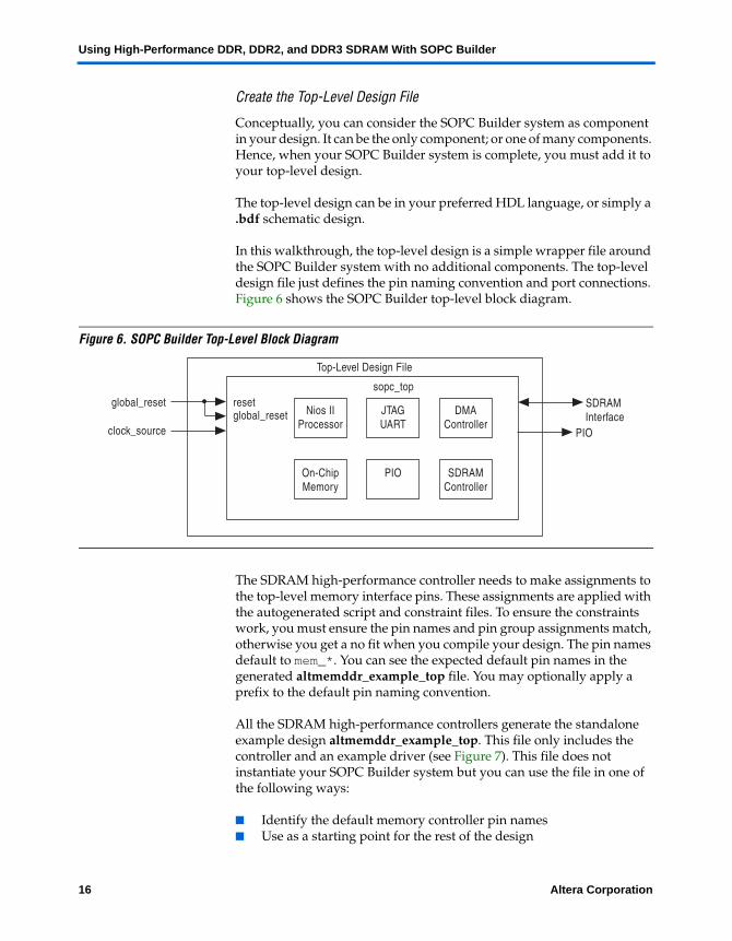
Create the Top-Level Design File
Conceptually, you can consider the SOPC Builder system as component in your design. It can be the only component; or one of many components. Hence, when your SOPC Builder system is complete, you must add it to your top-level design.
The top-level design can be in your preferred HDL language, or simply a .bdf schematic design.
In this walkthrough, the top-level design is a simple wrapper file around the SOPC Builder system with no additional components. The top-level design file just defines the pin naming convention and port connections. Figure 6 shows the SOPC Builder top-level block diagram.
Figure 6. SOPC Builder Top-Level Block Diagram
The SDRAM high-performance controller needs to make assignments to the top-level memory interface pins. These assignments are applied with the autogenerated script and constraint files. To ensure the constraints work, you must ensure the pin names and pin group assignments match, otherwise you get a no fit when you compile your design. The pin names default to mem_*. You can see the expected default pin names in the generated altmemddr_example_top file. You may optionally apply a prefix to the default pin naming convention.
All the SDRAM high-performance controllers generate the standalone example design altmemddr_example_top. This file only includes the controller and an example driver (see Figure 7). This file does not instantiate your SOPC Builder system but you can use the file in one of the following ways:
■ Identify the default memory controller pin names■ Use as a starting point for the rest of the design
Nios IIProcessor
JTAGUART
DMAController
On-ChipMemory
PIO
PIO
SDRAM Interface
global_resetglobal_resetreset
clock_source
sopc_top
Top-Level Design File
SDRAMController
16 6.1 Altera CorporationPreliminary
DDR2 SDRAM High-Performance Controller with SOPC Builder Walkthrough
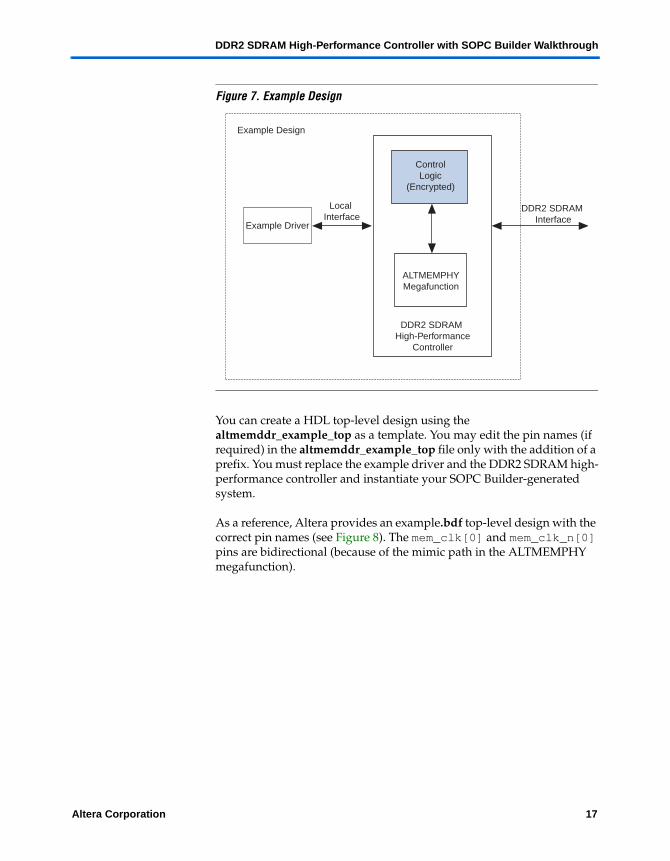
Figure 7. Example Design
You can create a HDL top-level design using the altmemddr_example_top as a template. You may edit the pin names (if required) in the altmemddr_example_top file only with the addition of a prefix. You must replace the example driver and the DDR2 SDRAM high-performance controller and instantiate your SOPC Builder-generated system.
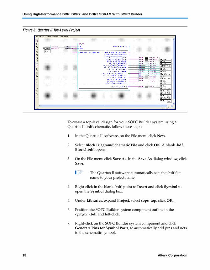
As a reference, Altera provides an example.bdf top-level design with the correct pin names (see Figure 8). The mem_clk[0] and mem_clk_n[0] pins are bidirectional (because of the mimic path in the ALTMEMPHY megafunction).
Example Driver
DDR2 SDRAM Interface
Local Interface
Example Design
Control Logic
(Encrypted)
DDR2 SDRAM High-Performance
Controller
ALTMEMPHYMegafunction
Altera Corporation 6.1 17Preliminary
Using High-Performance DDR, DDR2, and DDR3 SDRAM With SOPC Builder
Figure 8. Quartus II Top-Level Project
To create a top-level design for your SOPC Builder system using a Quartus II .bdf schematic, follow these steps:
1. In the Quartus II software, on the File menu click New.
2. Select Block Diagram/Schematic File and click OK. A blank .bdf, Block1.bdf, opens.
3. On the File menu click Save As. In the Save As dialog window, click Save.
1 The Quartus II software automatically sets the .bdf file name to your project name.
4. Right-click in the blank .bdf, point to Insert and click Symbol to open the Symbol dialog box.
5. Under Libraries, expand Project, select sopc_top, click OK.
6. Position the SOPC Builder system component outline in the <project>.bdf and left-click.
7. Right-click on the SOPC Builder system component and click Generate Pins for Symbol Ports, to automatically add pins and nets to the schematic symbol.
18 6.1 Altera CorporationPreliminary
DDR2 SDRAM High-Performance Controller with SOPC Builder Walkthrough
8. The autogenerated pin names match the SOPC Builder system pin names. Select each pin and manually change each pin name to match the equivalent pin name in altmemddr_example_top.
1 The SOPC Builder system includes the following unrequired signals for this example design, which you can disconnect:
• altmemddr_phy_clk_out • local_init_done_from_the_altmemddr• local_refresh_ack_from_the_altmemddr• local_wdata_req_from_the_altmemddr• reset_phy_clk_n_from_the_altmemddr
1 The following single vector signals require a [0] vectored pin name, otherwise simulation may fail:
• mem_dm• mem_dqs• mem_clk• mem_cke• mem_cs_n• mem_odt
9. The SOPC Builder System has two reset inputs, reset_n and global_reset_n_to_the_altmemddr. Connect both these signals to a single pin global_reset_n.
10. Ensure you rename the clock signal to clock_source.
f For more information on the signals, refer to the ALTMEMPHY Megafunction User Guide.
11. Change the name of out_port_from_the_pio[7..0] to pio[7..0].
14. On the File menu click Save, to save your changes.
15. On the Project menu click Set as Top-Level Entity.
Update the Quartus II Project Settings
To ensure the Quartus II project obtains optimum results, follow these steps:
1. On the Assignments menu click Settings. In the Category list, select Fitter Settings. For Fitter effort select Standard Fit (Highest Effort).
Altera Corporation 6.1 19Preliminary

Using High-Performance DDR, DDR2, and DDR3 SDRAM With SOPC Builder
2. In the Category list, select Analysis and Synthesis Settings. For Optimization Technique select Speed.
3. In the Category list, select Device. Click Device and Pin Options. Click the Unused Pins tab, for Reserve all unused pins select As input tri-stated with weak pull-up resistor.
4. Click the Voltage tab, for Default I/O standard select the same VCCIO voltage as the chosen SDRAM interface; for DDR2 SDRAM select 1.8 V. Click OK.
5. In the Category list, select Timing Analysis Settings, select TimeQuest Timing Analyzer During Compilation.
6. In the Category list, expand Timing Analysis Settings and select TimeQuest Timing Analyzer. Browse to the autogenerated altmemddr_phy_ddr_timing.sdc file and click Add. Click OK.
Specify the Top-Level Design Pin Out
Any DDR SDRAM interface must have its signals placed on the correct pin type and group. To specify the top-level design pin out, follow these steps:
1. On the Processing menu, point to Start and click Start Analysis and Synthesis.
2. Add pin I/O standard assignments:
a. If you are using the default pin names, run <variation_name>_pin_assignments.tcl. On the Tools menu click Tcl Scripts, select <variation name>_pin_ssignments.tcl and click Run.
or
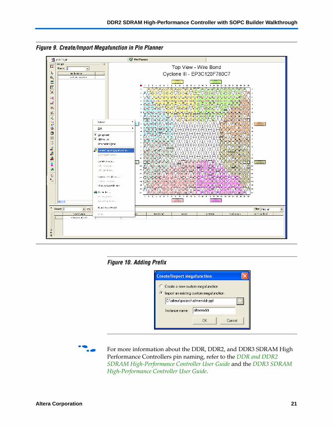
b. If you require pins name changes (prefix changes only) use the Quartus II Pin Planner and Import an existing custom megafunction.
• On the Assignment menu click Pin Planner.• Right-click in any area under Node Name and select
Create/Import Megafunction (see Figure 9).• Select Import an existing custom megafunction and select
the <variation name>.ppf file.• Type the prefix that you want to use in Instance name (see
Figure 10).
20 6.1 Altera CorporationPreliminary
DDR2 SDRAM High-Performance Controller with SOPC Builder Walkthrough
Figure 9. Create/Import Megafunction in Pin Planner
Figure 10. Adding Prefix
f For more information about the DDR, DDR2, and DDR3 SDRAM High Performance Controllers pin naming, refer to the DDR and DDR2 SDRAM High-Performance Controller User Guide and the DDR3 SDRAM High-Performance Controller User Guide.
Altera Corporation 6.1 21Preliminary
Using High-Performance DDR, DDR2, and DDR3 SDRAM With SOPC Builder
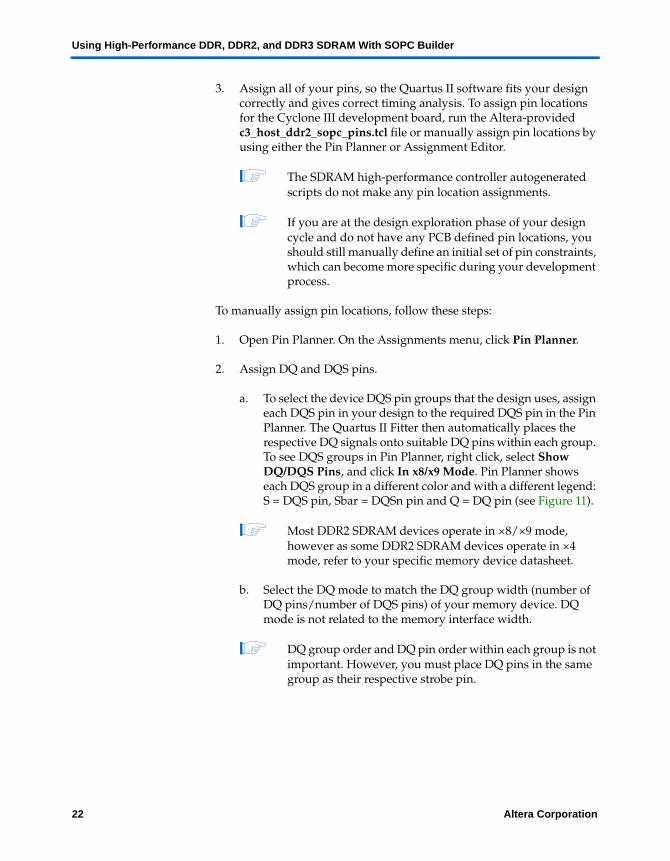
3. Assign all of your pins, so the Quartus II software fits your design correctly and gives correct timing analysis. To assign pin locations for the Cyclone III development board, run the Altera-provided c3_host_ddr2_sopc_pins.tcl file or manually assign pin locations by using either the Pin Planner or Assignment Editor.
1 The SDRAM high-performance controller autogenerated scripts do not make any pin location assignments.
1 If you are at the design exploration phase of your design cycle and do not have any PCB defined pin locations, you should still manually define an initial set of pin constraints, which can become more specific during your development process.
To manually assign pin locations, follow these steps:
1. Open Pin Planner. On the Assignments menu, click Pin Planner.
2. Assign DQ and DQS pins.
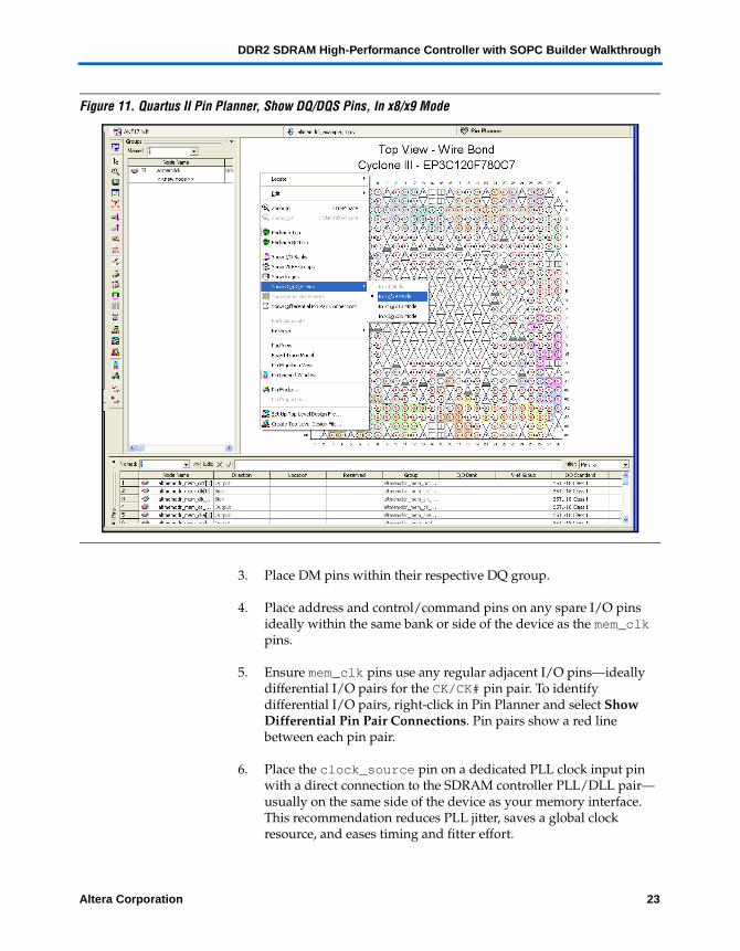
a. To select the device DQS pin groups that the design uses, assign each DQS pin in your design to the required DQS pin in the Pin Planner. The Quartus II Fitter then automatically places the respective DQ signals onto suitable DQ pins within each group. To see DQS groups in Pin Planner, right click, select Show DQ/DQS Pins, and click In x8/x9 Mode. Pin Planner shows each DQS group in a different color and with a different legend: S = DQS pin, Sbar = DQSn pin and Q = DQ pin (see Figure 11).
1 Most DDR2 SDRAM devices operate in ×8/×9 mode, however as some DDR2 SDRAM devices operate in ×4 mode, refer to your specific memory device datasheet.
b. Select the DQ mode to match the DQ group width (number of DQ pins/number of DQS pins) of your memory device. DQ mode is not related to the memory interface width.
1 DQ group order and DQ pin order within each group is not important. However, you must place DQ pins in the same group as their respective strobe pin.
22 6.1 Altera CorporationPreliminary
DDR2 SDRAM High-Performance Controller with SOPC Builder Walkthrough
Figure 11. Quartus II Pin Planner, Show DQ/DQS Pins, In x8/x9 Mode
3. Place DM pins within their respective DQ group.
4. Place address and control/command pins on any spare I/O pins ideally within the same bank or side of the device as the mem_clk pins.
5. Ensure mem_clk pins use any regular adjacent I/O pins—ideally differential I/O pairs for the CK/CK# pin pair. To identify differential I/O pairs, right-click in Pin Planner and select Show Differential Pin Pair Connections. Pin pairs show a red line between each pin pair.
6. Place the clock_source pin on a dedicated PLL clock input pin with a direct connection to the SDRAM controller PLL/DLL pair—usually on the same side of the device as your memory interface. This recommendation reduces PLL jitter, saves a global clock resource, and eases timing and fitter effort.
Altera Corporation 6.1 23Preliminary
Using High-Performance DDR, DDR2, and DDR3 SDRAM With SOPC Builder
7. Place the global_reset_n pin (like any high fan-out signal) on a dedicated clock pin.
f For more information on how to use the Quartus II Pin Planner, refer to the I/O Management chapter in volume 2 of the Quartus II Handbook.
f For more information on Cyclone III external memory pin selection, refer to the External Memory Interface in Cyclone III Devices chapter in the Cyclone III Device Handbook.
DDR2 SDRAM in Stratix III devices with differential DQS mode require mem_clk[0]/mem_clk_n[0] on a DIFFIO_RX capable pin pair. DDR3 SDRAM interfaces in Stratix III devices require mem_clk[0]/mem_clk_n[0] in any DQ or DQS pin pair with DIFFIO_RX capability.
f For more information on Stratix III external memory pin selection, refer to External Memory Interfaces in Stratix III Devices chapter in the Stratix III Device Handbook.
Compile the Design
To compile the design, on the Processing menu click Start Compilation.
Verify Memory Interface Timing
To verify memory interface timing, follow these steps:
1. On the Tools menu click Tcl Scripts.
2. Select <variation name>_phy_report_timing.tcl and click Run.
Test the Design On A Development Platform
To test the design on a development platform, follow these steps:
■ “Add the SignalTap II Logic Analyzer” on page 24■ “Compile the Project” on page 27■ “Verify Timing” on page 28
Add the SignalTap II Logic Analyzer
The SignalTap II logic analyzer shows read and write activity in the system.
f For more information on using the SignalTap II logic analyzer, refer to the following documents:
24 6.1 Altera CorporationPreliminary
DDR2 SDRAM High-Performance Controller with SOPC Builder Walkthrough
■ Design Debugging Using the SignalTap II Embedded Logic Analyzer chapter in the Quartus II Handbook
■ AN 323: Using SignalTap II Embedded Logic Analyzers in SOPC Builder Systems
■ AN 446: Debugging Nios II Systems with the SignalTap II Logic Analyzer
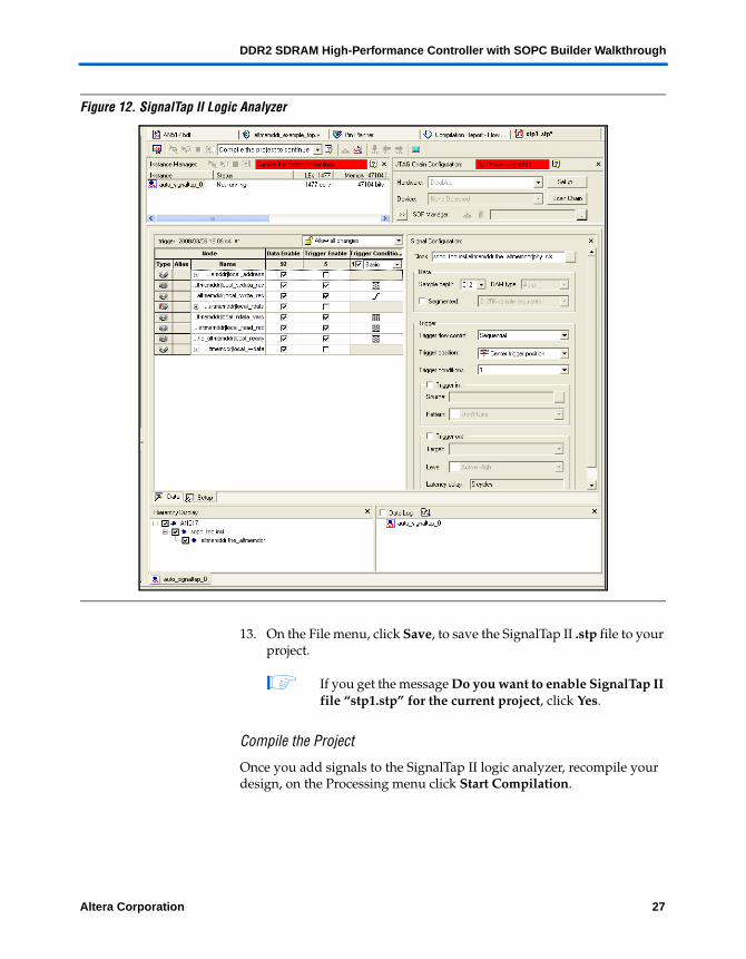
To add the SignalTap II logic analyzer, follow these steps:
1. On the Tools menu click SignalTap II Logic Analyzer.
2. In the Signal Configuration window next to the Clock box, click … (Browse Node Finder).
3. Type *phy_clk in the Named box, for Filter select SignalTap II: pre-synthesis and click List.
4. Select sopc_top:inst|altmemddr:the_altmemddr|phy_clk in Nodes Found and click > to add the signal to Selected Nodes.
5. Click OK.
6. Under Signal Configuration, specify the following settings:
● For Sample depth, select 512● For RAM type, select Auto (Stratix III devices only)● For Trigger flow control, select Sequential● For Trigger position, select Center trigger position● For Trigger conditions, select 1
7. On the Edit menu, click Add Nodes.
8. Search for specific nodes by typing *local* in the Named box, for Filter select SignalTap II: pre-synthesis and click List.
9. Select the following nodes in Nodes Found and click > to add to Selected Nodes:
● local_address● local_rdata● local_rdata_valid (alternative trigger to compare read/write
data)● local_read_req● local_ready● local_wdata● local_wdata_req● local_write_req (trigger)
Altera Corporation 6.1 25Preliminary
Using High-Performance DDR, DDR2, and DDR3 SDRAM With SOPC Builder
1 Do not add any DDR SDRAM interface signals to the SignalTap II logic analyzer. The load on these signals increases and adversely affects the timing analysis.
10. Click OK.
11. To reduce the SignalTap II logic size, turn off Trigger Enable on the following bus signals:
● local_address● local_rdata● local_wdata
12. Right-click Trigger Conditions for the local_write_req signal and select Rising Edge.
Figure 12 shows the completed SignalTap II logic analyzer.
26 6.1 Altera CorporationPreliminary
DDR2 SDRAM High-Performance Controller with SOPC Builder Walkthrough
Figure 12. SignalTap II Logic Analyzer
13. On the File menu, click Save, to save the SignalTap II .stp file to your project.
1 If you get the message Do you want to enable SignalTap II file “stp1.stp” for the current project, click Yes.
Compile the Project
Once you add signals to the SignalTap II logic analyzer, recompile your design, on the Processing menu click Start Compilation.
Altera Corporation 6.1 27Preliminary
Using High-Performance DDR, DDR2, and DDR3 SDRAM With SOPC Builder
Verify Timing
Once the design compiles, ensure that TimeQuest timing analysis passes successfully. In addition to this FPGA timing analysis, check your PCB or system SDRAM timing. To run timing analysis, run the *_phy_report_timing.tcl script.
1. On the Tools menu click Tcl Scripts.
2. Select <variation name>_phy_report_timing.tcl and click Run.
Connect the Development Board
Connect the Cyclone III development board to your computer.
For more information on the Cyclone III development board, refer to the Cyclone III Development Kit User Guide.
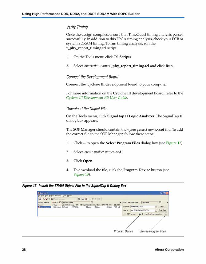
Download the Object File
On the Tools menu, click SignalTap II Logic Analyzer. The SignalTap II dialog box appears.
The SOF Manager should contain the <your project name>.sof file. To add the correct file to the SOF Manager, follow these steps:
1. Click ... to open the Select Program Files dialog box (see Figure 13).
2. Select <your project name>.sof.
3. Click Open.
4. To download the file, click the Program Device button (see Figure 13).
Figure 13. Install the SRAM Object File in the SignalTap II Dialog Box
Program Device Browse Program Files
28 6.1 Altera CorporationPreliminary
DDR2 SDRAM High-Performance Controller with SOPC Builder Walkthrough
Incorporate the Nios II IDE
You can now add test code to the project’s Nios II processor and use this program to run some simple tests.
When doing memory tests, you must read and write from the external DDR SDRAM and not from cached memory. The following three methods avoid using Nios II cached memory:
■ Use a Nios II processor that does not have cache memory, like the Nios II/s used in this example project.
■ Use the alt_remap_uncached function.
Launch Nios II IDE
To launch the Nios II IDE, follow these steps:
1. One the Tools menu, click SOPC Builder.
2. Click the System Generation tab.
3. Click Nios II IDE.
1 If it is the first time you have run the IDE, click Workbench.
4. On the File menu click Switch Workspace and select your project directory.
5. On the File menu point to New and click Project.
6. Expand Altera Nios II select Nios II C/C++ Application and click Next.
7. Select Blank Project under Select Project Templates and click Next.
8. Ensure that SOPC Builder System .ptf is <your project path>/<your sopc top>.ptf.
9. Click Next and click Finish.
10. In Windows Explorer drag Altera-supplied main.c to the blank_project_0 directory.
f To see the main.c example test program, see “Appendix: Example main.c Test Program File” on page 39.
Altera Corporation 6.1 29Preliminary
Using High-Performance DDR, DDR2, and DDR3 SDRAM With SOPC Builder
This program consists of a simple loop that takes commands from the JTAG UART and executes them. Table 2 shows the commands that are sent to the Nios II C code.
1 The commands must be in the following format and the switches A,B,C, and D must be entered in upper case. Both address and data strings must always be 8 characters long.
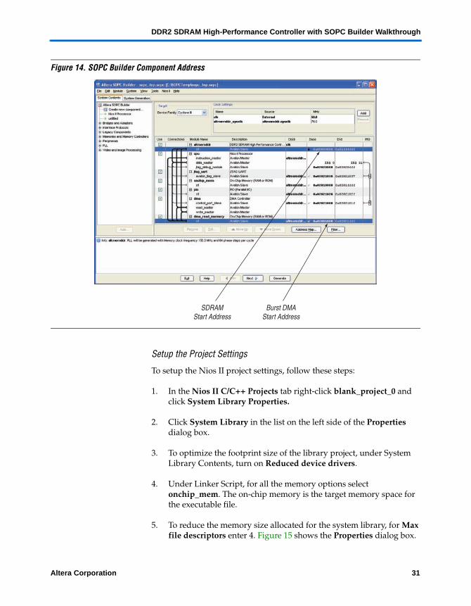
You can read the SOPC Builder component address locations directly from the SOPC Builder Window (see Figure 14).
Table 2. Commands
Command Format Description Example
Switch A Switch | Data Controls the LEDs. A000000FF. The last two bytes control all eight LEDs. The LEDs are active low on the board.
Switch B Switch | Address | Data Performs a single write to an address offset location in memory.
Enter B, followed by 00000000, then 00000001, writes 00000001 at SDRAM address offset location 00000000.
Switch C Switch | Address Performs a single read to an address offset location in memory.
Enter C, followed by 00000000, reads the contents of the memory at SDRAM address offset location 00000000.
Switch D Switch | From Address | To Address Performs an incremental write to the first address location, followed by a DMA burst transfer from the first address location to the second address location. The burst is a fixed length of 512 words or 2048 bytes.
D0200100000000000 loads the DMA read memory with the incrementing pattern, then DMA burst transfers it to the SDRAM high-performance controller.
30 6.1 Altera CorporationPreliminary
DDR2 SDRAM High-Performance Controller with SOPC Builder Walkthrough
Figure 14. SOPC Builder Component Address
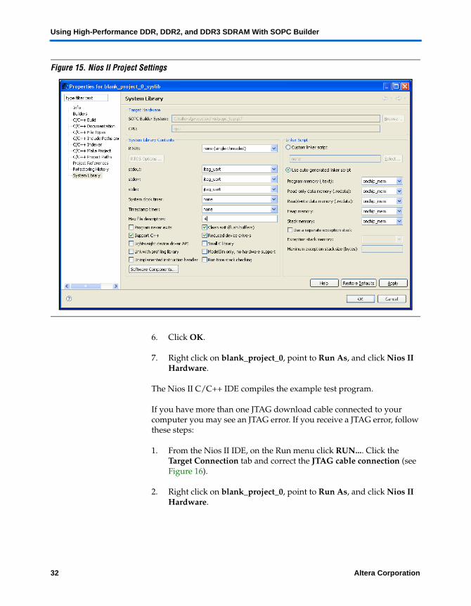
Setup the Project Settings
To setup the Nios II project settings, follow these steps:
1. In the Nios II C/C++ Projects tab right-click blank_project_0 and click System Library Properties.
2. Click System Library in the list on the left side of the Properties dialog box.
3. To optimize the footprint size of the library project, under System Library Contents, turn on Reduced device drivers.
4. Under Linker Script, for all the memory options select onchip_mem. The on-chip memory is the target memory space for the executable file.
5. To reduce the memory size allocated for the system library, for Max file descriptors enter 4. Figure 15 shows the Properties dialog box.
SDRAMStart Address
Burst DMAStart Address
Altera Corporation 6.1 31Preliminary
Using High-Performance DDR, DDR2, and DDR3 SDRAM With SOPC Builder
Figure 15. Nios II Project Settings
6. Click OK.
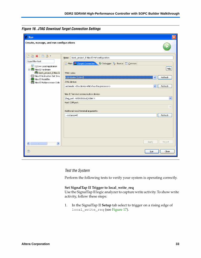
7. Right click on blank_project_0, point to Run As, and click Nios II Hardware.
The Nios II C/C++ IDE compiles the example test program.
If you have more than one JTAG download cable connected to your computer you may see an JTAG error. If you receive a JTAG error, follow these steps:
1. From the Nios II IDE, on the Run menu click RUN.... Click the Target Connection tab and correct the JTAG cable connection (see Figure 16).
2. Right click on blank_project_0, point to Run As, and click Nios II Hardware.
32 6.1 Altera CorporationPreliminary
DDR2 SDRAM High-Performance Controller with SOPC Builder Walkthrough
Figure 16. JTAG Download Target Connection Settings
Test the System
Perform the following tests to verify your system is operating correctly.
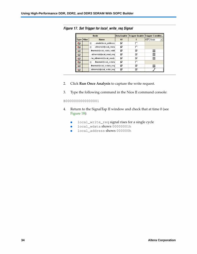
Set SignalTap II Trigger to local_write_reqUse the SignalTap II logic analyzer to capture write activity. To show write activity, follow these steps:
1. In the SignalTap II Setup tab select to trigger on a rising edge of local_write_req (see Figure 17).
Altera Corporation 6.1 33Preliminary
Using High-Performance DDR, DDR2, and DDR3 SDRAM With SOPC Builder
Figure 17. Set Trigger for local_write_req Signal
2. Click Run Once Analysis to capture the write request.
3. Type the following command in the Nios II command console:
B0000000000000001
4. Return to the SignalTap II window and check that at time 0 (see Figure 18):
● local_write_req signal rises for a single cycle● local_wdata shows 00000001h● local_address shows 000000h
34 6.1 Altera CorporationPreliminary
DDR2 SDRAM High-Performance Controller with SOPC Builder Walkthrough
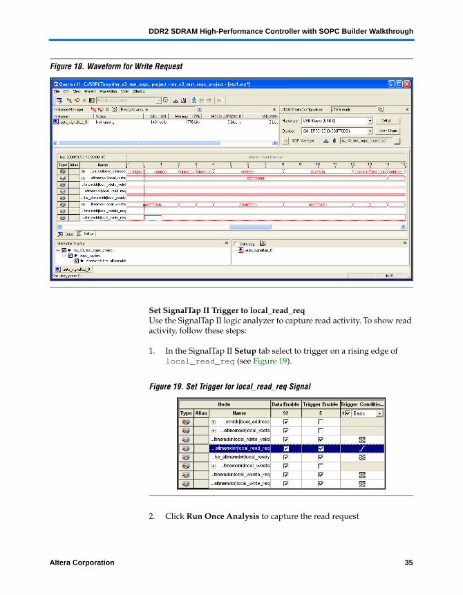
Figure 18. Waveform for Write Request
Set SignalTap II Trigger to local_read_reqUse the SignalTap II logic analyzer to capture read activity. To show read activity, follow these steps:
1. In the SignalTap II Setup tab select to trigger on a rising edge of local_read_req (see Figure 19).
Figure 19. Set Trigger for local_read_req Signal
2. Click Run Once Analysis to capture the read request
Altera Corporation 6.1 35Preliminary
Using High-Performance DDR, DDR2, and DDR3 SDRAM With SOPC Builder
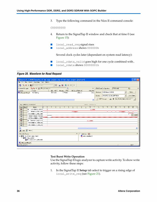
3. Type the following command in the Nios II command console:
C00000000
4. Return to the SignalTap II window and check that at time 0 (see Figure 15):
■ local_read_req signal rises■ local_address shows 000000h
Several clock cycles later (dependant on system read latency):
■ local_rdata_valid goes high for one cycle combined with..■ local_rdata shows 00000001h
Figure 20. Waveform for Read Request
Test Burst Write OperationUse the SignalTap II logic analyzer to capture write activity. To show write activity, follow these steps:
1. In the SignalTap II Setup tab select to trigger on a rising edge of local_write_req (see Figure 21).
36 6.1 Altera CorporationPreliminary
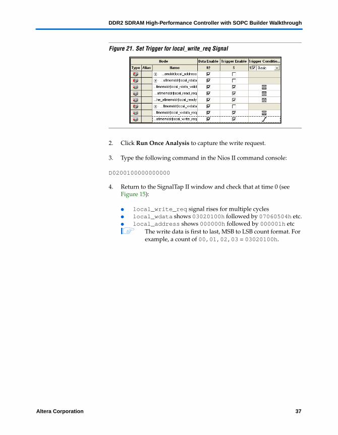
DDR2 SDRAM High-Performance Controller with SOPC Builder Walkthrough
Figure 21. Set Trigger for local_write_req Signal
2. Click Run Once Analysis to capture the write request.
3. Type the following command in the Nios II command console:
D0200100000000000
4. Return to the SignalTap II window and check that at time 0 (see Figure 15):
● local_write_req signal rises for multiple cycles● local_wdata shows 03020100h followed by 07060504h etc.● local_address shows 000000h followed by 000001h etc1 The write data is first to last, MSB to LSB count format. For
example, a count of 00,01,02,03 = 03020100h.
Altera Corporation 6.1 37Preliminary
Using High-Performance DDR, DDR2, and DDR3 SDRAM With SOPC Builder
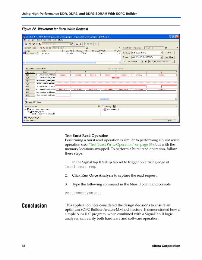
Figure 22. Waveform for Burst Write Request
Test Burst Read OperationPerforming a burst read operation is similar to performing a burst write operation (see “Test Burst Write Operation” on page 36), but with the memory locations swapped. To perform a burst read operation, follow these steps:
1. In the SignalTap II Setup tab set to trigger on a rising edge of local_read_req.
2. Click Run Once Analysis to capture the read request:
3. Type the following command in the Nios II command console:
D0000000002001000
Conclusion This application note considered the design decisions to ensure an optimum SOPC Builder Avalon-MM architecture. It demonstrated how a simple Nios II C program, when combined with a SignalTap II logic analyzer, can verify both hardware and software operation.
38 6.1 Altera CorporationPreliminary
Appendix: Example main.c Test Program File
You should consider carefully the following recommendations when combining a SDRAM high-performance controller with the SOPC Builder system interconnect fabric:
■ Minimize non-sequential addressing to reduce row addressing time.■ Match controller Avalon-MM interface width to Avalon-MM master
interface width.■ Match data cache size to memory burst length.■ Minimize multimaster designs where arbitration stalls may take
place.■ Remove or optimize clock domain crossing adapters.
Appendix: Example main.c Test Program File#include<stdio.h>#include"sys/alt_dma.h"#include "sys/alt_cache.h"#include "system.h"#include "altera_avalon_dma_regs.h"#define length 512int to_hex(char* pkt){ unsigned int value[8]; unsigned int value1=0; unsigned int q; for (q=0;q<=7;q++) { value[q]=(pkt[q]>0x39)?(pkt[q]-0x37):(pkt[q]-0x30);
if (q==0) { value1=(value1+value[q]); } else { value1=((value1<<4)+value[q]); }
} return value1;}
/******************************************************************* Function: Main_menu*
Altera Corporation 6.1 39Preliminary
Using High-Performance DDR, DDR2, and DDR3 SDRAM With SOPC Builder
* Purpose: Prints the main menu commands*******************************************************************/static void Main_menu(void){ printf("\n\n"); printf(" \n Select One of the following Commands \n"); printf( "\n Use Upper case \n"); printf(" \n Enter 'A' : Controls the LEDS:\n"); printf(" \n Enter 'B' : Single Write to an address location in Memory:\n"); printf(" \n Enter 'C' : Single Read to an address location in Memory:\n"); printf(" \n Enter 'D' : Performs DMA operation with burst length of 512 words:\n"); printf( "\n Enter your command now \n");
} /******************************************************************* Function: LED_Control** Purpose: Controls the LEDs..*******************************************************************/void LED_Control(void){ unsigned int led_value; unsigned char led[8]; printf(" \n LED Test opertaion \n"); printf( "\n Enter the value in Hex you want to write to the LEDs:(i.e. 000000FF)\n"); printf(" \n The last two bytes control all eight LEDs. \n"); gets(led); led_value=to_hex(&led[0]); printf(" \n Value to be displayed on LEDs is: %08x \n",led_value); IOWR_32DIRECT(LED_PIO_BASE,0, led_value);
}
/******************************************************************* Function: Single_Write** Purpose: Performs a single write to an address location in memory.*******************************************************************/void Single_Write(void){ unsigned char write_offset[8]; unsigned char data[8]; unsigned int DDR_write_OFFSET_ADDRESS; unsigned int write_data; printf(" \n Single Write opertaion \n");
40 6.1 Altera CorporationPreliminary
Appendix: Example main.c Test Program File
printf( "\n Enter the data you want to write to the Memory:(i.e. 44444444) \n"); gets(data); write_data=to_hex(&data[0]); printf( "\n Enter the offset address where you want to write in the Memory: (i.e. 00000010)\n"); gets(write_offset); DDR_write_OFFSET_ADDRESS = to_hex(&write_offset[0]); if ((DDR_write_OFFSET_ADDRESS<0)||(DDR_write_OFFSET_ADDRESS>=(ALTMEMDDR_SPAN/4))) { printf(" \n Invalid Offset \n"); printf( "\n You have entered wrong offset address : \n"); return; } IOWR(ALTMEMDDR_BASE,DDR_write_OFFSET_ADDRESS,write_data); if (IORD(ALTMEMDDR_BASE,DDR_write_OFFSET_ADDRESS)==write_data) { printf("\n Data: %08x is correctly written to memory offset: %08x \n", write_data,DDR_write_OFFSET_ADDRESS); printf("\n Write operation is done \n"); } else { printf("\n Write operation is Failed \n"); }} /******************************************************************* Function: Single_Read** Purpose: Performs a single read to an address location in memory*******************************************************************/void Single_Read(void){ unsigned char read_offset[8]; unsigned int DDR_read_OFFSET_ADDRESS; unsigned int read_data; printf(" \n Single Read opertaion \n"); printf( "\n Enter the offset address from where you want to read in the Memory:(i.e. 00000010) \n"); gets(read_offset); DDR_read_OFFSET_ADDRESS = to_hex(&(read_offset[0])); if ((DDR_read_OFFSET_ADDRESS<0) || (DDR_read_OFFSET_ADDRESS>=(ALTMEMDDR_SPAN/4))) { printf(" \n Invalid Offset \n"); } else { read_data=IORD(ALTMEMDDR_BASE,DDR_read_OFFSET_ADDRESS);
Altera Corporation 6.1 41Preliminary
Using High-Performance DDR, DDR2, and DDR3 SDRAM With SOPC Builder
printf("Read %08x from address %08x \n",read_data,(ALTMEMDDR_BASE+DDR_read_OFFSET_ADDRESS)); }}/******************************************************************* Function: Verify Operation** Purpose: Compares the memory contents of the read data master and write data master*******************************************************************/void Call_verify(unsigned char* source, unsigned char* destination){ if (memcmp(source,destination,(length*4))==0) { printf("\n DMA operation successful \n");
} else { printf("\n DMA operation failed \n"); printf( "\n Please check that DMA is correctly setup \n "); }}/******************************************************************* Function: DMA_Operation** Purpose: Performs an incremental write to the first addresslocation, followed by a DMA burst transfer from the first addresslocation to the second address location.The burst is a fixed length of 512 words or 2048 bytes.*******************************************************************/
Document Revision History
Table 3 shows the revision history for this application note.
Table 3. Document Revision History
Date and Document Version Changes Made Summary of Changes
March 2008 v1.0 First release. —
42 6.1 Altera CorporationPreliminary
Document Revision History
Altera Corporation 6.1 43Preliminary
101 Innovation DriveSan Jose, CA 95134Technical Support:www.altera.com/support/Literature Services:[email protected]
Copyright © 2008 Altera Corporation. All rights reserved. Altera, The Programmable Solutions Company,the stylized Altera logo, specific device designations, and all other words and logos that are identified astrademarks and/or service marks are, unless noted otherwise, the trademarks and service marks of AlteraCorporation in the U.S. and other countries. All other product or service names are the property of their re-spective holders. Altera products are protected under numerous U.S. and foreign patents and pendingapplications, maskwork rights, and copyrights. Altera warrants performance of its semiconductor productsto current specifications in accordance with Altera's standard warranty, but reserves the right to make chang-es to any products and services at any time without notice. Altera assumes no responsibility or liabilityarising out of the application or use of any information, product, or service describedherein except as expressly agreed to in writing by Altera Corporation. Altera customersare advised to obtain the latest version of device specifications before relying on any pub-lished information and before placing orders for products or services.