design implementation of ddr2 / ddr3 interfaces from a pcb
TRANSCRIPT

Michael Catrambone – Product Validation Engineer
RTP IPC Designers Council – March Chapter Meeting
Cisco Systems, Inc – Morrisville, NC
March 19, 2013
Design Implementation of DDR2 / DDR3 Interfaces From a PCB Designer Perspective in Cadence Allegro

2 © 2013 Cadence Design Systems, Inc. All Rights Reserved
• Extensive background in PCB development, Library Management, EDA Software support and value added Process Improvement. Expert using the Cadence Allegro PCB Tool Suite with Cadence Allegro DE HDL and
OrCAD schematic capture tools. – Over 24 years of successful experience in designing, developing and
implementing hardware solutions for the electronics industry.
– Product Validation Engineer for the Allegro Tool Suite at Cadence.
– Past work experience: Automated Systems (Military PCB Design & Fabrication / Prance Autorouter)
Cadence Design Systems (PCB Design / Certified Cadence Allegro Trainer)
USRobotics (OEM – Remote Access / Internet)
3Com Corporation (OEM – Network Switches / Servers)
CommWorks (OEM – Wireless / Wireline / VoiP)
UTStarcom (OEM – CDMA, Broadband and IP-based Communications)
Plexus Engineering Solutions (PCB Design and DFX Services Organization)
– Past Chairman of CDNLive – Cadence User Group (4 Years)
– Past ICU Board Member – International Cadence Users Group (7 Years)
About the Presenter… Michael Catrambone
3 © 2013 Cadence Design Systems, Inc. All Rights Reserved
• This presentation will discuss the layout challenges of implementing DDR2 and DDR3 interfaces on a Printed Circuit Board using best practices and design rule setup within Cadence Allegro.
• A brief overview of DDRx will be discussed as a point of general background on the interfaces to build the foundation for the presentation.
• Signal Integrity strategies for DDR2 and DDR3 interfaces will also be discussed but the main intent is to guide PCB Designers in configuring the Allegro design and Constraint Manager to route these interfaces effectively.
• As there are many different types of DDRx configuration (DIMM, SODIMM, On-Board, etc.), this presentation will focus on On-Board memory configuration only.
Abstract

4 © 2013 Cadence Design Systems, Inc. All Rights Reserved
Agenda
DDRx Memory Interfaces Overview
Interconnect Topologies
Placement and Pre-Route Techniques
DDRx Design Rules
Database Setup – XNET Generation
Electrical Constraint Management

5 © 2013 Cadence Design Systems, Inc. All Rights Reserved
Functional Groups (Controller)
Data
Data Mask
Data Strobe (differential _P & _N)
Address and Command
Control
Differential Clock
DDRx Memory Interfaces Overview Functional Group to Route Group Mapping
Route Groups (Memory)
BYTELANE0
BYTELANE1
BTYELANE2
BYTELANE3
BYTELANEn
Address and Command
Control
Differential Clock
DQ[7:0], DQ[15:8], DQ[16:23],DQ[31:25], …
DM0, DM1, DM2, DM3, …
DQS0, DQS1, DQS2, DQS3, …
CS, ODT, CKE
A[15:0], BA[2:0] / RAS, CAS, WE
CK_P, CK_N

6 © 2013 Cadence Design Systems, Inc. All Rights Reserved
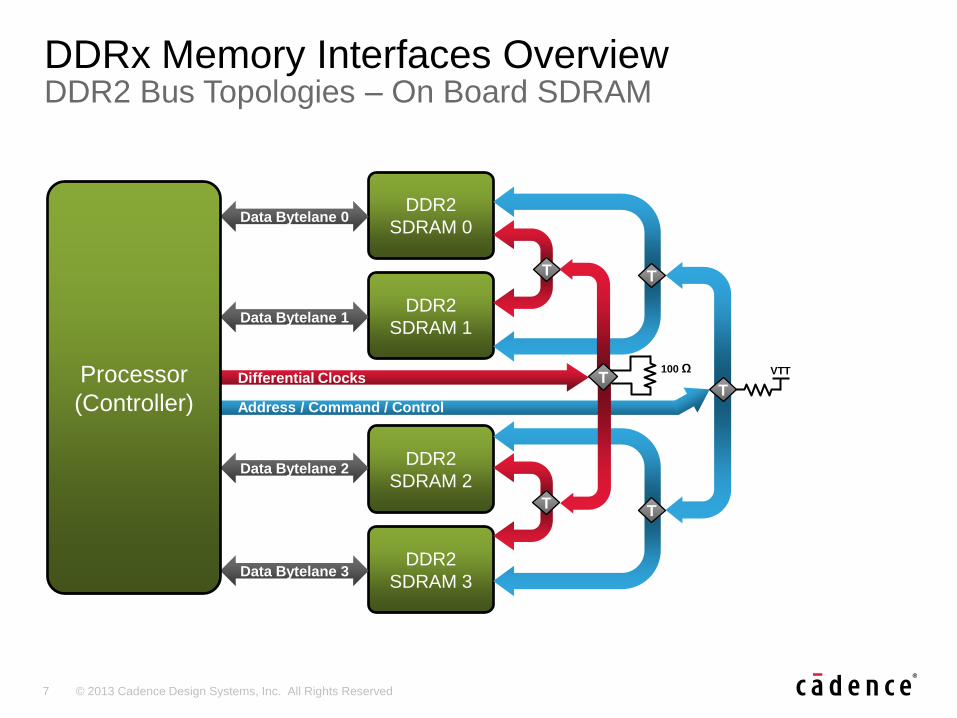
• Typical DDR2 and DDR3 Data Bus Structure:
BYTELANE0 DQ[7:0], DM0, DQS_P0, DQS_N0 BYTELANE1 DQ[15:8], DM1, DQS_P1, DQS_N1 BYTELANE2 DQ[23:16], DM2, DQS_P2, DQS_N2 BYTELANE3 DQ[31:24], DM3, DQS_P3, DQS_N3
BYTELANEn DQ[<8bits>], DMn, DQS_Pn, DQS_Nn
• Data Bytelane members should be routed on the same layer. – In some DDR2 memory applications the Data Strobe line may single ended.
• Address / Command / Control / Differential Clocks should be routed on the same layer but if space issues arise they could route on different layers. – Adjacent layers or layers referencing the same plane layer is preferred.
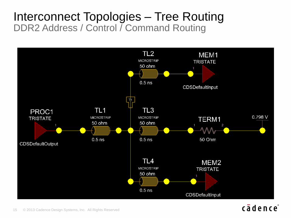
• Address / Command / Control / Differential Clocks route topology differences – DDR2 Interfaces: Routed using a Symmetrical Tree route topology.
– Routed to a central t-point with balanced routed legs to each of the Memory IC’s
– DDR3 Interfaces: Routed using a Daisy Chain (Fly-by) topology. Route from controller starting with Chip 0 thru Chip n routing in order by Bytelane numbers
– Chip 0 is the lower data bit (Bytelane0) / Chip n is the upper data bit (Bytelane3).
DDRx Memory Interfaces Overview General Design Requirements
7 © 2013 Cadence Design Systems, Inc. All Rights Reserved
DDRx Memory Interfaces Overview DDR2 Bus Topologies – On Board SDRAM
DDR2
SDRAM 0
DDR2
SDRAM 1
DDR2
SDRAM 2
DDR2
SDRAM 3
Data Bytelane 1
Differential Clocks
T
Data Bytelane 0
Data Bytelane 2
Data Bytelane 3
T
VTT
T
Address / Command / Control
Processor
(Controller)
T
T
T 100 Ω

8 © 2013 Cadence Design Systems, Inc. All Rights Reserved
Three Differential Clocks per UDIMM
DDRx Memory Interfaces Overview DDR2 Bus Topologies – On Board Four-UDIMM
Data Bytelane (5 Per two Connectors)
Differential Clock (1 Per Connector)
Address / Command / Control
Data Bytelane (5 per two Connectors)
Data Bytelane (4 Per two Connectors)
Data Bytelane (4 per two Connectors)
Address / Command / Control
Address / Command / Control
Address / Command / Control
Differential Clock (1 Per Connector)
Differential Clock (1 Per Connector)
VTT
Processor
(Controller)
VTT
VTT
VTT

9 © 2013 Cadence Design Systems, Inc. All Rights Reserved
DDR3
SDRAM 0
Address / Command / Control
• Data Bus Termination – Series resistor termination
could be used when the point to point connection is in the 2” to 2.5” range. – Resistors located at the center
of the transmission line.
– DRAM Termination with direct connect using On-Die termination (ODT) – Better signal quality and lower
cost compared to using series resistor termination.
• Clock Termination – 100ohm Differential
terminator at last DDR3 device in the chain.
DDRx Memory Interfaces Overview DDR3 Bus Topologies – On Board SDRAM
DDR3
SDRAM 1
DDR3
SDRAM 2
DDR3
SDRAM 3
Differential Clocks
Processor
(Controller)
100 Ω
VTT
Data Bytelane 1
Data Bytelane 0
Data Bytelane 2
Data Bytelane 3

10 © 2013 Cadence Design Systems, Inc. All Rights Reserved
DDRx Memory Interfaces Overview DDR3 Bus Topologies – On Board Two-UDIMM
Differential Clock
Address / Command / Control
Address / Command / Control
Differential Clock
Differential Clock
Two Differential Clocks per UDIMM
VTT
VTT
VTT VTT
VTT VTT
• 1 Cycle Timing (1T) has two sets of Address / Command / Control, driven by the memory controller, connecting to each connector, as shown
• 2 Cycle Timing (2T) has one set of Address / Command / Control connecting to both connectors.
• VTT termination resistors are not required on the main board as they are built into the DDR3 modules
Data Bytelane (5 Per two Connectors)
Data Bytelane (4 Per two Connectors)
Differential Clock
Processor
(Controller)

11 © 2013 Cadence Design Systems, Inc. All Rights Reserved
• Relative Propagation Delay – Data Bytelane 200mils between all members inside of Bytelane
– Address / Command / Control 200 – 300mils between Controller and T-Point
25 – 50mils between memory ICs and T-Point
• Propagation Delay – Normally not constraint controlled as it is driven by placement of the memory
ICs, which should be placed as close to the Controller as possible, normally between 750 – 1000mils between Memory ICs. Package type is also a driving factor, ICs vs. DIMM Connector.
• Differential Phase Tolerance – 25mils for all Data Strobe and Clock Differential Pairs
• Disclaimer: The above rules are for reference only and should be treated as such. The only tried and true way to determine interface design rules is with Pre/Post Route simulations
DDRx Memory Interfaces Overview DDR2 Electrical Constraint Targets
12 © 2013 Cadence Design Systems, Inc. All Rights Reserved
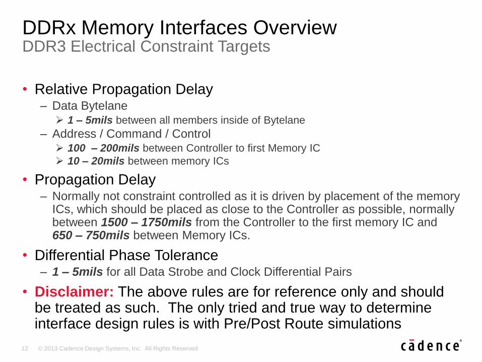
• Relative Propagation Delay – Data Bytelane 1 – 5mils between all members inside of Bytelane
– Address / Command / Control 100 – 200mils between Controller to first Memory IC
10 – 20mils between memory ICs
• Propagation Delay – Normally not constraint controlled as it is driven by placement of the memory
ICs, which should be placed as close to the Controller as possible, normally between 1500 – 1750mils from the Controller to the first memory IC and 650 – 750mils between Memory ICs.
• Differential Phase Tolerance – 1 – 5mils for all Data Strobe and Clock Differential Pairs
• Disclaimer: The above rules are for reference only and should be treated as such. The only tried and true way to determine interface design rules is with Pre/Post Route simulations
DDRx Memory Interfaces Overview DDR3 Electrical Constraint Targets

13 © 2013 Cadence Design Systems, Inc. All Rights Reserved
• Impedance Requirements – Single Ended Target = 50 – 60 Ohms
– Differential Pair Target = 100 – 120 Ohms
• Design Stack-up considerations – All routing should have a solid reference plane to provide a low-impedance
path for return currents.
– Never route traces over splits or voids in the plane, including via voids.
– The entire Data Bytelane should be routed on the same layer, including Data Mask and Data Strobe Differential Pairs.
– To avoid any possible crosstalk between layers develop a stack-up which utilizes strip-line routing layers for critical routing vs. dual strip-line..
– To minimize any via stub effects route all connections on the furthest layer opposite the memory ICs.
DDRx Memory Interfaces Overview Impedance / Design Stack-up
Stripline Dual Striplines

14 © 2013 Cadence Design Systems, Inc. All Rights Reserved
• Impedance Requirements – Single Ended Target = 50 – 60 Ohms
– Differential Pair Target = 100 – 120 Ohms
• Design Stack-up considerations – All routing should have a solid reference plane to provide a low-impedance
path for return currents.
– Never route traces over splits or voids in the plane, including via voids.
– The entire Data Bytelane should be routed on the same layer, including Data Mask and Data Strobe Differential Pairs.
– To avoid any possible crosstalk between layers develop a stack-up which utilizes strip-line routing layers for critical routing vs. dual strip-line..
– To minimize any via stub effects route all connections on the furthest layer opposite the memory ICs.
DDRx Memory Interfaces Overview Impedance / Design Stack-up
Stripline Dual Striplines
Reference Plane
Signal Layer
Reference Plane
Signal Layer
Reference Plane
Signal Layer
Reference Plane
Signal Layer
Reference Plane
Signal Layer
Signal Layer
Reference Plane
Reference Plane
Signal Layer
Signal Layer
Reference Plane
15 © 2013 Cadence Design Systems, Inc. All Rights Reserved
Interconnect Topologies – Tree Routing DDR2 Address / Control / Command Routing

16 © 2013 Cadence Design Systems, Inc. All Rights Reserved
Interconnect Topologies – Daisy Chain Routing DDR3 Address / Control / Command Routing
17 © 2013 Cadence Design Systems, Inc. All Rights Reserved
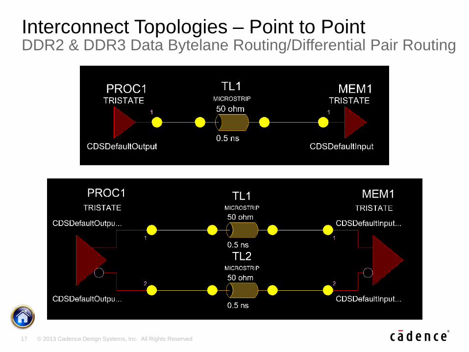
Interconnect Topologies – Point to Point DDR2 & DDR3 Data Bytelane Routing/Differential Pair Routing

18 © 2013 Cadence Design Systems, Inc. All Rights Reserved
• Careful planning of Memory chips or DIMM connectors placement to allow the best possible path for routing.
• Reserve space for pin escape (fanout), termination resistors as well as termination power supplies.
• For DDR2 interfaces: – Spread out Memory chips to accommodate for tree routing, via t-point area
for Address, Command and Control routes. – Approximate spacing between Memory chips should be no less than 300mils
• For DDR3 interfaces: – Locate Memory chips to allow Address / Command / Control / Differential
Clock Daisy Chain (Fly-by) routing starting at the Controller then connecting to the lowest data bit chip first (Bytelane0) progressing up the Bytelane numbers and ending at the highest data bit chip. – Approximate spacing between Memory chips should be no less than 200mils to
allow matching outside of the Via/BGA Field of the devices.
Placement Techniques Component Placement

19 © 2013 Cadence Design Systems, Inc. All Rights Reserved
• Spread vias out to allow routing of at least two traces between vias, where possible, while maintaining reference to adjacent plane layers. (avoid routing thru via voids in the plane)
• Keep in mind the interconnect topologies of the pins that you are escaping. – Share vias to form a t-point for the address bus remembering to have room
to match them on the surface of the board.
Placement Techniques Pin Escaping (Fanout)

20 © 2013 Cadence Design Systems, Inc. All Rights Reserved
Placement Techniques – DDR1: 8 Bytelanes Two top side memory ICs via sharing with bottom side ICs

21 © 2013 Cadence Design Systems, Inc. All Rights Reserved
Placement Techniques – DDR1: 8 Bytelanes Three bottom side memory ICs via sharing with top side ICs
22 © 2013 Cadence Design Systems, Inc. All Rights Reserved
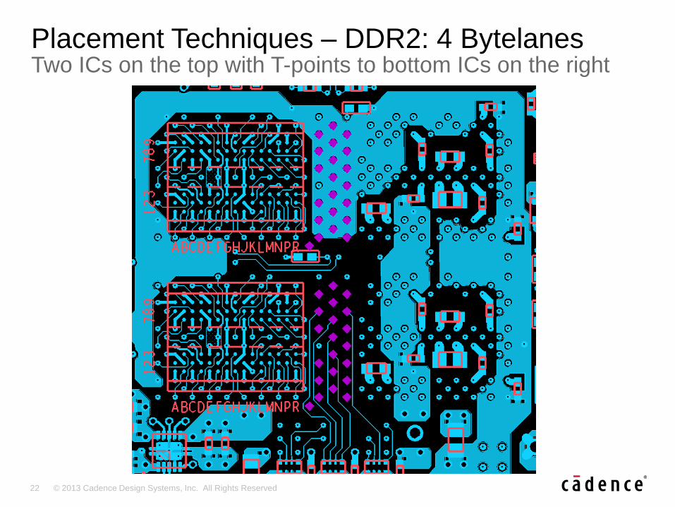
Placement Techniques – DDR2: 4 Bytelanes Two ICs on the top with T-points to bottom ICs on the right

23 © 2013 Cadence Design Systems, Inc. All Rights Reserved
Placement Techniques – DDR2: 4 Bytelanes Two ICs on the bottom with T-points to top ICs on the right

24 © 2013 Cadence Design Systems, Inc. All Rights Reserved
Placement Techniques – DDR3: 4 Bytelanes .8mm ICs on top – Notice fanout to increase routing channels

25 © 2013 Cadence Design Systems, Inc. All Rights Reserved
Placement Techniques – DDR3: 4 Bytelanes Partial Address bus and 1 Data Bytelane routed on surface

26 © 2013 Cadence Design Systems, Inc. All Rights Reserved
• Pin and Gate Swapping – Pin Swapping: Data bits (DQ[63:0])can be swapped within a
Bytelane to improve routing. – Excludes Data Mask (DM[7:0]) and Data Strobe(DQS[7:0])
– Gate Swapping: All members of one Bytelane can be swapped with all members of another Bytelane.
• Ultimately, you need to be thinking about routing these critical connections during the placement stage in your design and allocating adequate space to meet matching requirements and routing topologies.
Placement Techniques Pre-Route planning

27 © 2013 Cadence Design Systems, Inc. All Rights Reserved
• Enabling these options will provide DRC feedback when placing components that do not meet the delay requirements.
• Rules will be checked using Manhattan distances of Ratsnest connections.
Placement Techniques Electrical Options – DRC Unrouted (Setup > Constraints > Modes)

28 © 2013 Cadence Design Systems, Inc. All Rights Reserved
• Automated method of moving Virtual Rat-Ts (diamonds) to the t-point location, on top of a via or trace t-junction. – You can move these Virtual Rat-Ts manually, one at a time, using the
Move command as well.
• Allows a more accurate unrouted DRC check to ensure Delay rules are realistic.
• After the routing is complete it provides a good visual representation of t-points locations to assist in delaying the appropriate connect lines (clines).
Pre-Route Techniques Optimize Rat-Ts (Route > PCB Router > Optimize Rat Ts)

29 © 2013 Cadence Design Systems, Inc. All Rights Reserved
• How it works: – Routine actually goes into Allegro PCB Router (Specctra) to perform
the updates.
– Earlier versions of Allegro had unexpected results but as of v16.3 this functionality has greatly improved.
• Things to do before executing: – With any automated task, be sure to save the design prior to running
the command to avoid any lost of work.
– Nets that are fixed will be ignored and the Virtual Rat-Ts will not be optimized.
– To avoid a known issue, all nets should be Fixed accept the nets that you want the Virtual Rat-Ts optimized. – Routine will rip-up stitch vias during optimization if the Net is not Fixed.
Pre-Route Techniques Optimize Rat-Ts (Route > PCB Router > Optimize Rat Ts)

30 © 2013 Cadence Design Systems, Inc. All Rights Reserved
Pre-Route Techniques Ratsnest and Virtual Rat-Ts prior to running Optimizing Rat-Ts
31 © 2013 Cadence Design Systems, Inc. All Rights Reserved
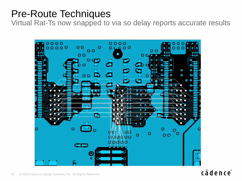
Pre-Route Techniques Virtual Rat-Ts now snapped to via so delay reports accurate results

32 © 2013 Cadence Design Systems, Inc. All Rights Reserved
• Creating an alias to generate a popup describing the issue and what should be done first prior to running this command.
alias optimize_ts 'skill axlUIConfirm(" ## WARNING ##
Before running Optimize Rat-Ts, you MUST fix all nets
except the nets that you would like the Rat-Ts
optimized. This command may remove stitch vias during
optimization and the only workaround is to fix all other
nets first. When you have fixed all other nets you can
bypass this message by typing OPTIMIZE_TS_NOW on the
Allegro Command Line to run the optimization")'
alias optimize_ts_now "\optimize_ts"
• These two entries can be added to your local env file or added to site configuration in the site.env
Pre-Route Techniques Maintain Design Integrity / Alert User / Workaround Issue

33 © 2013 Cadence Design Systems, Inc. All Rights Reserved
• Creating an alias to generate a popup describing the issue and what should be done first prior to running this command.
alias optimize_ts 'skill axlUIConfirm(" ## WARNING ##
Before running Optimize Rat-Ts, you MUST fix all nets
except the nets that you would like the Rat-Ts
optimized. This command may remove stitch vias during
optimization and the only workaround is to fix all other
nets first. When you have fixed all other nets you can
bypass this message by typing OPTIMIZE_TS_NOW on the
Allegro Command Line to run the optimization")'
alias optimize_ts_now "\optimize_ts"
• These two entries can be added to your local env file or added to site configuration in the site.env
Pre-Route Techniques Maintain Design Integrity / Alert User / Workaround Issue

34 © 2013 Cadence Design Systems, Inc. All Rights Reserved
• As tolerances get tighter you can include Package and Z-Axis Delays in the DRC calculations to ensure rules are being met.
• These settings should be considered when planning out the electrical rules on any high speed interfaces.
• Design Stack-up must be defined with all the appropriate thicknesses based on a Fabricator approved stack-up for this additional Z-Axis check to be accurate.
• Depth (distance) the signal travels down the via or pin holes will be added to the delay calculations.
• NOTE: Allegro PCB Designer license with the High-Speed option is required to utilize this functionality otherwise the rules will be ignored.
Design Rules Electrical Options – Z Axis Delay (Setup > Constraints > Modes)

35 © 2013 Cadence Design Systems, Inc. All Rights Reserved
• As tolerances get tighter you can include Package and Z-Axis Delays in the DRC calculations to ensure rules are being met.
• These settings should be considered when planning out the electrical rules on any high speed interfaces.
• Design Stack-up must be defined with all the appropriate thicknesses based on a Fabricator approved stack-up for this additional Z-Axis check to be accurate.
• Depth (distance) the signal travels down the via or pin holes will be added to the delay calculations.
• NOTE: Allegro PCB Designer license with the High-Speed option is required to utilize this functionality otherwise the rules will be ignored.
Design Rules Electrical Options – Z Axis Delay (Setup > Constraints > Modes)
36 © 2013 Cadence Design Systems, Inc. All Rights Reserved
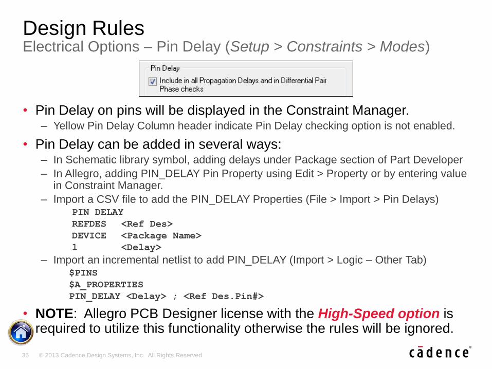
• Pin Delay on pins will be displayed in the Constraint Manager. – Yellow Pin Delay Column header indicate Pin Delay checking option is not enabled.
• Pin Delay can be added in several ways: – In Schematic library symbol, adding delays under Package section of Part Developer
– In Allegro, adding PIN_DELAY Pin Property using Edit > Property or by entering value in Constraint Manager.
– Import a CSV file to add the PIN_DELAY Properties (File > Import > Pin Delays) PIN DELAY
REFDES <Ref Des>
DEVICE <Package Name>
1 <Delay>
– Import an incremental netlist to add PIN_DELAY (Import > Logic – Other Tab) $PINS
$A_PROPERTIES
PIN_DELAY <Delay> ; <Ref Des.Pin#>
• NOTE: Allegro PCB Designer license with the High-Speed option is required to utilize this functionality otherwise the rules will be ignored.
Design Rules Electrical Options – Pin Delay (Setup > Constraints > Modes)

37 © 2013 Cadence Design Systems, Inc. All Rights Reserved
Database Setup – XNET Generation Click “here” to skip to Electrical Constraints Management

38 © 2013 Cadence Design Systems, Inc. All Rights Reserved
• eXtended Net through passive devices such as a resistor or capacitor which allows electrical design rules to be applied from IC Pin to IC Pin.
Constraint Management What is a XNET?
< NET >
Net Name: DDR_DQ23
Member of XNet: DDR_DQ23
Member of Bus: DDR_BYTELANE2
Pin count: 2
Via count: 0
Total etch length: 313.647 MIL
Total manhattan length: 365.938 MIL
Percent manhattan: 85.71%
Pin Type SigNoise Model
--- ---- --------------
U2.4 BI CDSDefaultIO_2p5v
RP1.1 UNSPEC RNX0008300_50
< NET >
Net Name: DDR_RDQ23
Member of XNet: DDR_DQ23
Member of Bus: DDR_BYTELANE2
Pin count: 2
Via count: 2
Total etch length: 1313.598 MIL
Total manhattan length: 1396.252 MIL
Percent manhattan: 94.08%
Pin Type SigNoise Model
--- ---- --------------
U1.F3 BI CDSDefaultIO_2p5v
RP1.8 UNSPEC RNX0008300_50

39 © 2013 Cadence Design Systems, Inc. All Rights Reserved
• Define PCB Stack-up based on PCB Fabricator recommendations (Setup > Cross Section) – Include dielectric layer/thickness between each of the Conductor
layers, Conductor layer thickness, Dielectric Constant and Loss Tangent based on PCB board material called out.
– Z Axis delay relies on an accurate stack-up to properly check rules when including the via in delay calculations.
– Used by the Field Solver to provide accurate transmission line modeling of traces.
– Used to determines trace characteristics such as Impedance, Inductance, Capacitance, Propagation Delay and Resistance. (Display > Parasitics)
– Impedance calculations may not match the data provided from the PCB Fabricator but the trace width recommendation should always be based on the Fabricator stack-up.
Database Setup Accurate Design Stack-up

40 © 2013 Cadence Design Systems, Inc. All Rights Reserved
Database Setup Allegro Cross Section vs. Fabricator Stack-up Model
41 © 2013 Cadence Design Systems, Inc. All Rights Reserved
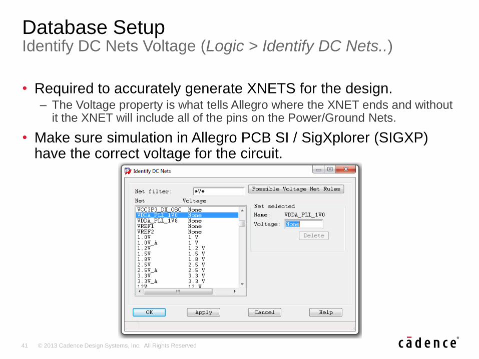
• Required to accurately generate XNETS for the design. – The Voltage property is what tells Allegro where the XNET ends and without
it the XNET will include all of the pins on the Power/Ground Nets.
• Make sure simulation in Allegro PCB SI / SigXplorer (SIGXP) have the correct voltage for the circuit.
Database Setup Identify DC Nets Voltage (Logic > Identify DC Nets..)
42 © 2013 Cadence Design Systems, Inc. All Rights Reserved
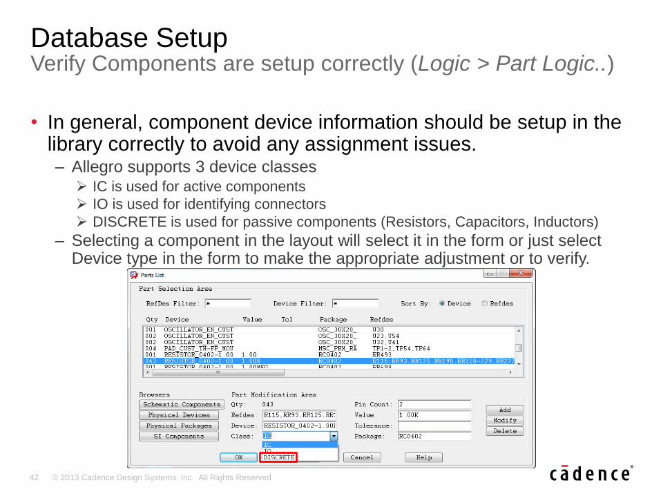
• In general, component device information should be setup in the library correctly to avoid any assignment issues. – Allegro supports 3 device classes IC is used for active components
IO is used for identifying connectors
DISCRETE is used for passive components (Resistors, Capacitors, Inductors)
– Selecting a component in the layout will select it in the form or just select Device type in the form to make the appropriate adjustment or to verify.
Database Setup Verify Components are setup correctly (Logic > Part Logic..)

43 © 2013 Cadence Design Systems, Inc. All Rights Reserved
• Device CLASS and Symbol pin PINUSE are closely related, the following are the supported PINUSE for each CLASS: – IC = IN, OUT, BI, NC, GROUND, POWER, TRI, OCA or OCL
– IO = UNSPEC
– DISCRETE = UNSPEC
• Device CLASS and Pin PINUSE definitions need to be correct in order for the appropriate model assignment to occur.
• It also is used when applying Electrical Constraint Sets (ECSET) to XNETS in your design if incorrect could cause mapping issues.
• Most of these issues can be corrected prior to v16.5 using the Setup Advisor (Tools > Setup Advisor) but in v16.5 forward it was revamped and now called SI Design Setup (Setup > SI Design Setup..)
• It is recommended that this information be setup correctly in one place, the EDA Library, to avoid having to run thru these updates for every design.
Database Setup Verify Components are setup correctly

44 © 2013 Cadence Design Systems, Inc. All Rights Reserved
• Assigning ESpice models to the passive components will combine the nets to form XNETS by running Model Assignment. – Model Assignment will run a SI Audit which analyzes all the nets in the
design to determine which nets it considers to be Power/Ground (DC Net) then reports the nets which are missing the Voltage property.
XNET Generation Model Assignment (Analyze > Model Assignment..) SI Audit

45 © 2013 Cadence Design Systems, Inc. All Rights Reserved
• You can select the net(s) in the SI Design Audit form to resolve the errors and add the Voltage Property.
– To select multiple rows hold the Ctrl Key or use the Shift Key to pick start and stop
– “All” or “Selected” buttons will generate a Voltage value based on the net name.
– “Manually “button will allow you to enter the Voltage value for each net name.
XNET Generation Model Assignment (Analyze > Model Assignment..) SI Audit

46 © 2013 Cadence Design Systems, Inc. All Rights Reserved
Voltage Property assignment using the “All” or “Selected” buttons.
Voltage Property assignment using the “Manually” button.
XNET Generation Model Assignment (Analyze > Model Assignment..) SI Audit

47 © 2013 Cadence Design Systems, Inc. All Rights Reserved
• You can also select the net(s) in the SI Design Audit form that are not Power/Ground and set them to Ignore so they are not reported again.
– “All” button will ignore all nets reported the next a SI Audit is ran.
– “Selected” button will ignore the selected nets the next time SI Audit is ran.
XNET Generation Model Assignment (Analyze > Model Assignment..) SI Audit
48 © 2013 Cadence Design Systems, Inc. All Rights Reserved
XNET Generation Signal Model Assignment
• Once all Voltage errors are resolved or ignored you will be presented with the Signal Model Assignment form.
• Selecting a component in the layout will select it in the form or just select reference designator or device type in form then press the “Create Model” button.
• Optionally, you can select the “Auto Setup” button to create ESpice models for all components which have been classified as DISCRETE.
• These models are generated and stored internally in the database. – Also models are written to the devices.dml file in the same directory
as the database.

49 © 2013 Cadence Design Systems, Inc. All Rights Reserved
XNET Generation Signal Model Assignment
• Once all Voltage errors are resolved or ignored you will be presented with the Signal Model Assignment form.
• Selecting a component in the layout will select it in the form or just select reference designator or device type in form then press the “Create Model” button.
• Optionally, you can select the “Auto Setup” button to create ESpice models for all components which have been classified as DISCRETE.
• These models are generated and stored internally in the database. – Also models are written to the devices.dml file in the same directory
as the database.

50 © 2013 Cadence Design Systems, Inc. All Rights Reserved
XNET Generation Manual ESpice Model Generation examples

51 © 2013 Cadence Design Systems, Inc. All Rights Reserved
• After some generic database setup, defining Voltage on PWR/GND nets and adding ESpice models to passive components, XNETS will be generated correctly.
• Here are some advantages of having XNETS in your design: – Ability to apply Constraints across multiple nets looking thru passive
components inside of Constraint Manager
– XNET Name for the combined net will be the net name which is alphabetically highest net name. (Net A + Net B will form XNET A)
– Only the XNET name will appear in Constraint Manager, Nets suppressed.
– Generate Electrical Constraints Sets based on these newly formed XNETS which could then be applied across the several XNETS or buses of XNETS.
– Visualize the XNET topology inside of SigXplorer and easily assign electrical rules that can be pushed back to Constraint Manager.
– Right mouse button on XNet / Net in Constraint Manager and select SigXplorer to display the topology.
– NOTE: Allegro PCB Designer license with the High-Speed option is required to access the SigXplorer functionality.
Electrical Constraints Management Electrical Constraint Set (ECSET) and Topology Generation

52 © 2013 Cadence Design Systems, Inc. All Rights Reserved
Electrical Constraints Management

53 © 2013 Cadence Design Systems, Inc. All Rights Reserved
Electrical Constraints Management Visualize XNET in SigXplorer (SIGXP) – DDR3 Address Bus
Voltage Tap automatically
generated based on Voltage
Property assignment

54 © 2013 Cadence Design Systems, Inc. All Rights Reserved
Copy a Transmission line
in SigXplorer to generate a
T-Point in Allegro
Electrical Constraints Management Visualize XNET – DDR2 Address Bus with T-point generated

55 © 2013 Cadence Design Systems, Inc. All Rights Reserved
Copy a Transmission line
in SigXplorer to generate a
T-Point in Allegro
Two Transmission lines will
form a T-point in Allegro
Electrical Constraints Management Visualize XNET – DDR2 Address Bus with T-point generated

56 © 2013 Cadence Design Systems, Inc. All Rights Reserved
Electrical Constraints Management Driving Electrical rules from inside of SigXplorer
• Define electrical rules for the XNET (Set > Constraints) – Propagation Delay, Relative Propagation Delay, Differential Pair, etc.
• Inside the Set Topology Constraints form you can select the t-points or pins in the form or on the canvas to quickly define the pin to pin or pin to t-point rules. (Also can be done in Constraint Manager)

57 © 2013 Cadence Design Systems, Inc. All Rights Reserved
Electrical Constraints Management Optional Component in Topology
• The power of a Topology is that it allows you to apply rules across multiple nets on a particular bus.
• In some cases there may be an unique bit(s) on the bus which does not have the same topology, i.e. series resistor, pullup, etc.
• This situation will cause the Topology mapping to fail with a pin mismatch but you can make that particular component in the topology Optional so the mapping completes successfully. – Using Set > Optional Pins then select the component on the canvas to set it
as an Optional component.

58 © 2013 Cadence Design Systems, Inc. All Rights Reserved
• After you finish defining the Electrical rules for the Topology you need to save the updates into Constraint Manager before closing SigXplorer – File > Update Constraint Manager will update Constraint Manager
– When prompted, Select No to just create the Electrical Constraint Set (ECSet) and not to associate it to the XNet / Net you originally selected in to load into SigXplorer.
Electrical Constraints Management Updating Constraint Manager with rules defined in SigXplorer

59 © 2013 Cadence Design Systems, Inc. All Rights Reserved
• RMB on top of ECSET name to rename it to something more generic.
• After you finish defining the Electrical rules for the Topology you need to save the updates into Constraint Manager before closing SigXplorer – File > Update Constraint Manager will update Constraint Manager
– When prompted, Select No to just create the Electrical Constraint Set (ECSet) and not to associate it to the XNet / Net you originally selected in to load into SigXplorer.
Electrical Constraints Management Updating Constraint Manager with rules defined in SigXplorer

60 © 2013 Cadence Design Systems, Inc. All Rights Reserved
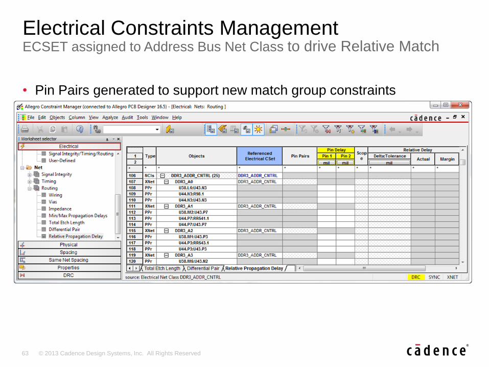
• It is possible to assign an ECSET to each of the XNETS individually but it is recommended to add them to a Net Class for ECSET assignment.
– Select the XNETS inside of the Electrical Spreadsheet then via RMB: – Select Create > Class to create a new Net Class
– or Select Membership > Class to add them to an existing Net Class
Electrical Constraints Management Create Address Bus Net Class for ECSET assignment

61 © 2013 Cadence Design Systems, Inc. All Rights Reserved
• It is possible to assign an ECSET to each of the XNETS individually but it is recommended to add them to a Net Class for ECSET assignment.
– Select the XNETS inside of the Electrical Spreadsheet then via RMB: – Select Create > Class to create a new Net Class
– or Select Membership > Class to add them to an existing Net Class
Electrical Constraints Management Create Address Bus Net Class for ECSET assignment

62 © 2013 Cadence Design Systems, Inc. All Rights Reserved
• Assign ECSET to Address Bus Net Class
Electrical Constraints Management ECSET assigned to Address Bus Net Class to drive Relative Match
63 © 2013 Cadence Design Systems, Inc. All Rights Reserved
• Assign ECSET to Address Bus Net Class
Electrical Constraints Management ECSET assigned to Address Bus Net Class to drive Relative Match
• Pin Pairs generated to support new match group constraints

64 © 2013 Cadence Design Systems, Inc. All Rights Reserved
• Assign ECSET to Address Bus Net Class
Electrical Constraints Management ECSET assigned to Address Bus Net Class to drive Relative Match
• Pin Pairs generated to support new match group constraints
• Relative Propagation Delay match groups are created

65 © 2013 Cadence Design Systems, Inc. All Rights Reserved
Electrical CSet: "DDR3_ADDR_CNTRL" (Revision: "1.0")
DDR3_ADDR_CNTRL (NetClass)
DDR3_A0 (Net): Apply status...
Date/Time: Sun Jan 20 16:57:02 2013
Mapping Pins of Cset: DDR3_ADDR_CNTRL
Mapping Mode: Pinuse and Refdes
Cset end point Xnet end point mapping mode
---------------------------- -------------------- ------------------------------
DDR3_PV_BOARD_MAC_TMP R98.1 DDR3_PV_BOARD R98.1 Approximate Refdes & Pinnumber
DDR3_PV_BOARD_MAC_TMP U44.N3 DDR3_PV_BOARD U44.N3 Refdes & Pinnumber
DDR3_PV_BOARD_MAC_TMP U43.N3 DDR3_PV_BOARD U43.N3 Refdes & Pinnumber
DDR3_PV_BOARD_MAC_TMP U38.L6 DDR3_PV_BOARD U38.L6 Refdes & Pinnumber
Net Schedule: Template Defined
DDR3_PV_BOARD U44.N3->DDR3_PV_BOARD U43.N3
DDR3_PV_BOARD U44.N3->DDR3_PV_BOARD R98.1
DDR3_PV_BOARD U43.N3->DDR3_PV_BOARD U38.L6
Prop Delay: DDR3_PV_BOARD U44.N3 to DDR3_PV_BOARD R98.1 min=0 MIL max=825 MIL
Prop Delay: DDR3_PV_BOARD U44.N3 to DDR3_PV_BOARD U43.N3 min=0 MIL max=825 MIL
Prop Delay: DDR3_PV_BOARD U38.L6 to DDR3_PV_BOARD U43.N3 min=0 MIL max=1750 MIL
Relative Prop Delay: GLOBAL group SDRAM2_TO_TERM DDR3_PV_BOARD U44.N3 to DDR3_PV_BOARD R98.1 delta= tol=20 MIL
Relative Prop Delay: GLOBAL group SDRAM1_TO_SDRAM2 DDR3_PV_BOARD U44.N3 to DDR3_PV_BOARD U43.N3 delta= tol=20 MIL
Relative Prop Delay: GLOBAL group P1011_TO_SDRAM1 DDR3_PV_BOARD U38.L6 to DDR3_PV_BOARD U43.N3 delta= tol=300 MIL
Electrical Constraints Management Electrical Constraint mapping report log window

66 © 2013 Cadence Design Systems, Inc. All Rights Reserved
Electrical CSet: "DDR3_ADDR_CNTRL" (Revision: "1.0")
DDR3_ADDR_CNTRL (NetClass)
DDR3_A1 (Net): Apply status...
Date/Time: Sun Jan 20 16:57:02 2013
Mapping Pins of Cset: DDR3_ADDR_CNTRL
Mapping Mode: Pinuse and Refdes
Cset end point Xnet end point mapping mode
---------------------------- --------------------- ------------------
DDR3_PV_BOARD_MAC_TMP R98.1 DDR3_PV_BOARD RR541.1 Approximate Pinuse
DDR3_PV_BOARD_MAC_TMP U44.N3 DDR3_PV_BOARD U44.P7 Refdes
DDR3_PV_BOARD_MAC_TMP U43.N3 DDR3_PV_BOARD U43.P7 Refdes
DDR3_PV_BOARD_MAC_TMP U38.L6 DDR3_PV_BOARD U38.M2 Refdes
Net Schedule: Template Defined
DDR3_PV_BOARD U44.P7->DDR3_PV_BOARD U43.P7
DDR3_PV_BOARD U44.P7->DDR3_PV_BOARD RR541.1
DDR3_PV_BOARD U43.P7->DDR3_PV_BOARD U38.M2
Prop Delay: DDR3_PV_BOARD U44.P7 to DDR3_PV_BOARD RR541.1 min=0 MIL max=825 MIL
Prop Delay: DDR3_PV_BOARD U44.P7 to DDR3_PV_BOARD U43.P7 min=0 MIL max=825 MIL
Prop Delay: DDR3_PV_BOARD U38.M2 to DDR3_PV_BOARD U43.P7 min=0 MIL max=1750 MIL
Relative Prop Delay: GLOBAL group SDRAM2_TO_TERM DDR3_PV_BOARD U44.P7 to DDR3_PV_BOARD RR541.1 delta= tol=20 MIL
Relative Prop Delay: GLOBAL group SDRAM1_TO_SDRAM2 DDR3_PV_BOARD U44.P7 to DDR3_PV_BOARD U43.P7 delta= tol=20 MIL
Relative Prop Delay: GLOBAL group P1011_TO_SDRAM1 DDR3_PV_BOARD U38.M2 to DDR3_PV_BOARD U43.P7 delta= tol=300 MIL
Electrical Constraints Management Electrical Constraint mapping report log window

67 © 2013 Cadence Design Systems, Inc. All Rights Reserved
– Select the NETS inside of the Electrical Spreadsheet then via RMB: – Select Create > Class to create a new Net Class
– or Select Membership > Class to add them to an existing Net Class
– Net Class creation is not limited to XNETS, can contain NETS as well.
Electrical Constraints Management Create Net Class for each of the Data Bus Bytelanes

68 © 2013 Cadence Design Systems, Inc. All Rights Reserved
– Select the NETS inside of the Electrical Spreadsheet then via RMB: – Select Create > Class to create a new Net Class
– or Select Membership > Class to add them to an existing Net Class
– Net Class creation is not limited to XNETS, can contain NETS as well.
Electrical Constraints Management Create Net Class for each of the Data Bus Bytelanes

69 © 2013 Cadence Design Systems, Inc. All Rights Reserved
Electrical Constraints Management Create ECSETs for each of the Data Bus Bytelanes

70 © 2013 Cadence Design Systems, Inc. All Rights Reserved
Electrical Constraints Management Create ECSETs for each of the Data Bus Bytelanes

71 © 2013 Cadence Design Systems, Inc. All Rights Reserved
Electrical Constraints Management Create ECSETs for each of the Data Bus Bytelanes

72 © 2013 Cadence Design Systems, Inc. All Rights Reserved
• Create separate ECSET for each Data Bytelane Match Group
Electrical Constraints Management Individual ECSETs per Data Bus Bytelane to drive Relative Match

73 © 2013 Cadence Design Systems, Inc. All Rights Reserved
• Create separate ECSET for each Data Bytelane Match Group
Electrical Constraints Management Individual ECSETs per Data Bus Bytelane to drive Relative Match
• Assign specific ECSET to each Data Bus Bytelane Net Class

74 © 2013 Cadence Design Systems, Inc. All Rights Reserved
• Create separate ECSET for each Data Bytelane Match Group
Electrical Constraints Management Individual ECSETs per Data Bus Bytelane to drive Relative Match
• Assign specific ECSET to each Data Bus Bytelane Net Class • Relative Propagation Delay Match Groups are created

75 © 2013 Cadence Design Systems, Inc. All Rights Reserved
• Create ECSET for all Data Bus Bytelanes with generic Match Group name
Electrical Constraints Management One ECSET for all Data Bus Bytelanes to drive Relative Match

76 © 2013 Cadence Design Systems, Inc. All Rights Reserved
• Create ECSET for all Data Bus Bytelanes with generic Match Group name
Electrical Constraints Management One ECSET for all Data Bus Bytelanes to drive Relative Match
• Assign ECSET to each Data Bus Bytelane Net Class

77 © 2013 Cadence Design Systems, Inc. All Rights Reserved
• Create ECSET for all Data Bus Bytelanes with generic Match Group name
Electrical Constraints Management One ECSET for all Data Bus Bytelanes to drive Relative Match
• Assign ECSET to each Data Bus Bytelane Net Class • Relative Propagation Delay Match Groups are created

78 © 2013 Cadence Design Systems, Inc. All Rights Reserved
• Create ECSET for all Data Bus Bytelanes with generic Match Group name
Electrical Constraints Management One ECSET for all Data Bus Bytelanes to drive Relative Match
• Assign ECSET to each Data Bus Bytelane Net Class • Relative Propagation Delay Match Groups are created • ECSET Match Group Name + Net Class Name = Match Group Name

79 © 2013 Cadence Design Systems, Inc. All Rights Reserved
• This presentation only scratched the surface on what can be done in Cadence Allegro to expedite and manage constraints effectively.
• Doing the upfront design setup will make the process go that much smoother and allow for simulations to be easily performed throughout the design cycle.
• It is possible to generate XNET constraints inside of Constraint Manager without utilizing SigXplorer but the amount of time would be greatly increased on designs with several complex buses.
• Electrical Constraint Sets (ECSETs) can be generated without the use of a Topology but using SigXplorer gives you a visual representation of the circuit to provide a higher level of understanding of what needs to be done.
• ECSETs with or without a Topology can be saved off and reused on other designs to maintain a consistent rule base for similar interfaces and circuitry.
Conclusion

80 © 2013 Cadence Design Systems, Inc. All Rights Reserved