tps51206 2-a peak sink / source ddr termination regulator ... · tps51206 2-a peak sink / source...
TRANSCRIPT
1
2
7
9
3
5
4
6
VTT
VTTSNS
PGND
VTTREF
VDDQSNS
VLDOIN
S3
S5
TPS51206
10 VDD
8GND
PowerPad
VTT
VTTREFS3_SLP
S5_SLP
5 V or 3.3 V Supply
VDDQ
Copyright © 2016, Texas Instruments Incorporated
Product
Folder
Order
Now
Technical
Documents
Tools &
Software
Support &Community
An IMPORTANT NOTICE at the end of this data sheet addresses availability, warranty, changes, use in safety-critical applications,intellectual property matters and other important disclaimers. PRODUCTION DATA.
TPS51206SLUSAH1E –MAY 2011–REVISED JULY 2018
TPS51206 2-A Peak Sink / Source DDR Termination Regulator With VTTREF BufferedReference for DDR2, DDR3, DDR3L, and DDR4
1
1 Features1• Supply Input Voltage: Supports 3.3-V Rail and 5-V
Rail• VLDOIN Input Voltage Range: VTT+0.4 V to 3.5 V• VTT Termination Regulator
– Output Voltage Range: 0.5 V to 0.9 V– 2-A Peak Sink and Source Current– Requires Only 10-μF MLCC Output Capacitor– ±20 mV Accuracy
• VTTREF Buffered Reference– VDDQ/2 ± 1% Accuracy– 10-mA Sink and Source Current
• Supports High-Z in S3 and Soft-Stop in S4 and S5with S3 and S5 Inputs
• Overtemperature Protection• 10-Pin, 2 mm × 2 mm SON (DSQ) Package
2 Applications• DDR2, DDR3, DDR3L, and DDR4 Memory Power
Supplies• SSTL_18, SSTL_15, SSTL_135 and HSTL
Termination• Telecom and Datacom, GSM Base Station, LCD-
TV and PDP-TV, Copier and Printer, Set-top Box
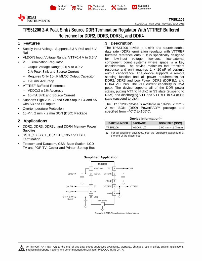
3 DescriptionThe TPS51206 device is a sink and source doubledate rate (DDR) termination regulator with VTTREFbuffered reference output. It is specifically designedfor low-input voltage, low-cost, low-externalcomponent count systems where space is a keyconsideration. The device maintains fast transientresponse and only requires 1 × 10-µF of ceramicoutput capacitance. The device supports a remotesensing function and all power requirements forDDR2, DDR3 and Low-Power DDR3 (DDR3L), andDDR4 VTT bus. The VTT current capability is ±2-Apeak. The device supports all of the DDR powerstates, putting VTT to High-Z in S3 state (suspend toRAM) and discharging VTT and VTTREF in S4 or S5state (suspend to disk).
The TPS51206 device is available in 10-Pin, 2 mm ×2 mm SON (DSQ) PowerPAD™ package andspecified from –40°C to 105°C.
Device Information(1)
PART NUMBER PACKAGE BODY SIZE (NOM)TPS51206 WSON (10) 2.00 mm × 2.00 mm
(1) For all available packages, see the orderable addendum atthe end of the datasheet.
Simplified Application
2
TPS51206SLUSAH1E –MAY 2011–REVISED JULY 2018 www.ti.com
Product Folder Links: TPS51206
Submit Documentation Feedback Copyright © 2011–2018, Texas Instruments Incorporated
Table of Contents1 Features .................................................................. 12 Applications ........................................................... 13 Description ............................................................. 14 Revision History..................................................... 25 Pin Configuration and Functions ......................... 36 Specifications......................................................... 4
6.1 Absolute Maximum Ratings ...................................... 46.2 ESD Ratings.............................................................. 46.3 Recommended Operating Conditions....................... 46.4 Thermal Information .................................................. 46.5 Electrical Characteristics........................................... 56.6 Typical Characteristics .............................................. 6
7 Detailed Description ............................................ 107.1 Overview ................................................................. 107.2 Functional Block Diagram ....................................... 107.3 Feature Description................................................. 107.4 Device Functional Modes........................................ 12
8 Application and Implementation ........................ 138.1 Application Information............................................ 138.2 Typical Applications ................................................ 13
9 Power Supply Recommendations ...................... 1710 Layout................................................................... 17
10.1 Layout Guidelines ................................................. 1710.2 Layout Example .................................................... 1810.3 Thermal Considerations ....................................... 18
11 Device and Documentation Support ................. 1911.1 Device Support...................................................... 1911.2 Receiving Notification of Documentation Updates 1911.3 Community Resources.......................................... 1911.4 Trademarks ........................................................... 1911.5 Electrostatic Discharge Caution............................ 1911.6 Glossary ................................................................ 19
12 Mechanical, Packaging, and OrderableInformation ........................................................... 19
4 Revision HistoryNOTE: Page numbers for previous revisions may differ from page numbers in the current version.
Changes from Revision D (March 2018) to Revision E Page
• Changed "specified from –40°C to 85°C" to "specified from –40°C to 105°C" in Description .............................................. 1• Changed maximum operating temperature from "85 °C" to "105 °C" in Recommended Operating Conditions table ........... 4
Changes from Revision C (August 2016) to Revision D Page
• Added VTTREF tolerance at 100 μA condition ..................................................................................................................... 5
Changes from Revision B (December 2014) to Revision C Page
• Added references to DDR4 compatibility .............................................................................................................................. 1• Added Receiving Notification of Documentation Updates section ....................................................................................... 19• Added Community Resources section ................................................................................................................................. 19
Changes from Revision A (October 2013) to Revision B Page
• Added Pin Configuration and Functions section, ESD Ratings table, Feature Description section, Device FunctionalModes, Application and Implementation section, Power Supply Recommendations section, Layout section, Deviceand Documentation Support section, and Mechanical, Packaging, and Orderable Information section .............................. 1
Changes from Original (MAY 2011) to Revision A Page
• Added minimum and maximum values to the wake up condition of the VDD UVLO threshold voltage specification ........... 5
VDD
S5
S3
VTTREF
VDDQSNS
VLDOIN
VTT
PGND
1
2
3
4
5
10
9
8
7
6
GND
VTTSNS
Thermal Pad
3
TPS51206www.ti.com SLUSAH1E –MAY 2011–REVISED JULY 2018
Product Folder Links: TPS51206
Submit Documentation FeedbackCopyright © 2011–2018, Texas Instruments Incorporated
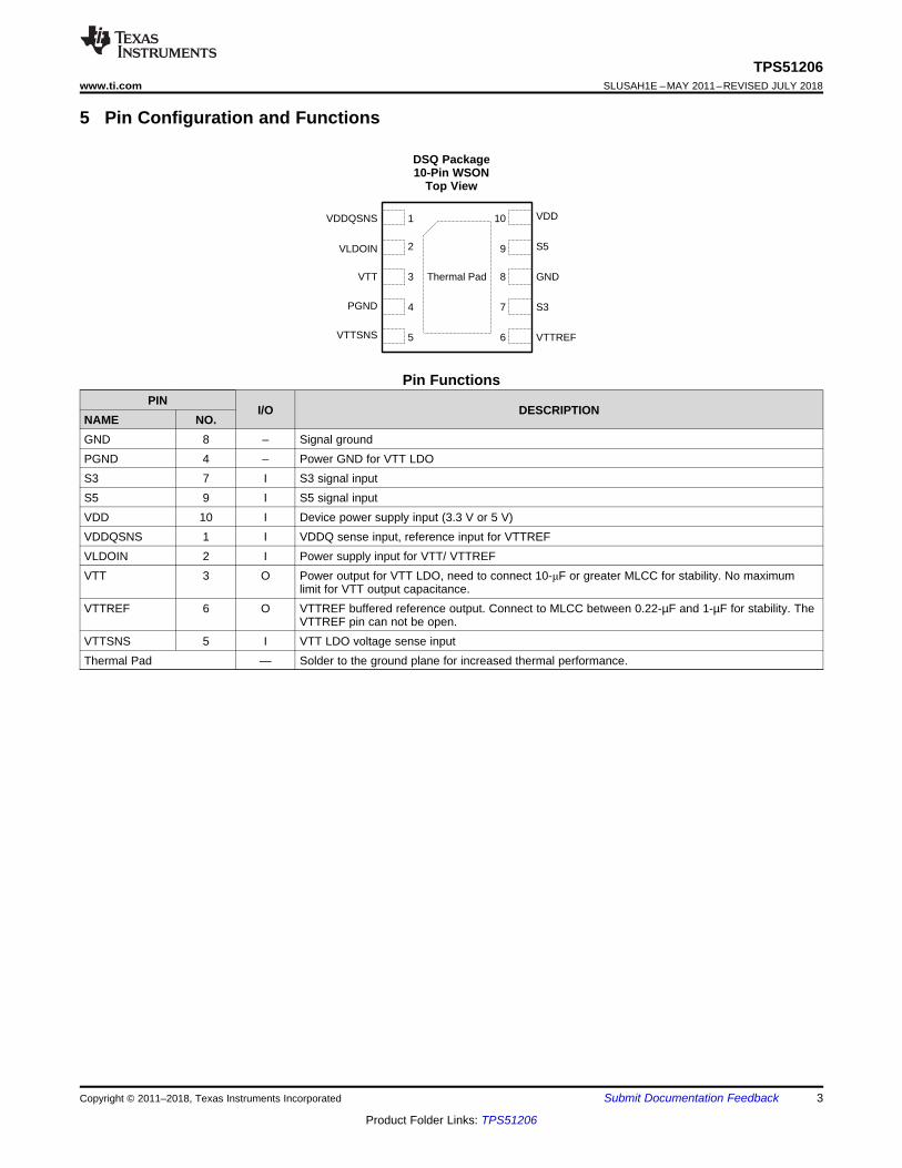
5 Pin Configuration and Functions
DSQ Package10-Pin WSON
Top View
Pin FunctionsPIN
I/O DESCRIPTIONNAME NO.GND 8 – Signal groundPGND 4 – Power GND for VTT LDOS3 7 I S3 signal inputS5 9 I S5 signal inputVDD 10 I Device power supply input (3.3 V or 5 V)VDDQSNS 1 I VDDQ sense input, reference input for VTTREFVLDOIN 2 I Power supply input for VTT/ VTTREFVTT 3 O Power output for VTT LDO, need to connect 10-μF or greater MLCC for stability. No maximum
limit for VTT output capacitance.VTTREF 6 O VTTREF buffered reference output. Connect to MLCC between 0.22-µF and 1-µF for stability. The
VTTREF pin can not be open.VTTSNS 5 I VTT LDO voltage sense inputThermal Pad — Solder to the ground plane for increased thermal performance.
4
TPS51206SLUSAH1E –MAY 2011–REVISED JULY 2018 www.ti.com
Product Folder Links: TPS51206
Submit Documentation Feedback Copyright © 2011–2018, Texas Instruments Incorporated
(1) Stresses beyond those listed under Absolute Maximum Ratings(1) may cause permanent damage to the device. These are stress ratingsonly and functional operation of the device at these or any other conditions beyond those indicated under Recommended OperatingConditions is not implied. Exposure to absolute-maximum-rated conditions for extended periods may affect device reliability.
(2) All voltage values are with respect to the network ground terminal unless otherwise noted.
6 Specifications
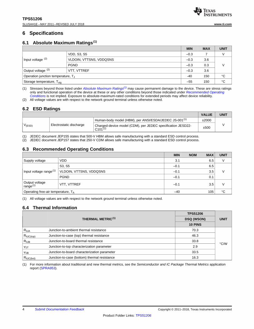
6.1 Absolute Maximum Ratings (1)
MIN MAX UNIT
Input voltage (2)
VDD, S3, S5 –0.3 7 VVLDOIN, VTTSNS, VDDQSNS –0.3 3.6
VPGND –0.3 0.3Output voltage (2) VTT, VTTREF –0.3 3.6Operation junction temperature, TJ -40 150 °CStorage temperature, Tstg –55 150 °C
(1) JEDEC document JEP155 states that 500-V HBM allows safe manufacturing with a standard ESD control process.(2) JEDEC document JEP157 states that 250-V CDM allows safe manufacturing with a standard ESD control process.
6.2 ESD RatingsVALUE UNIT
V(ESD) Electrostatic dischargeHuman-body model (HBM), per ANSI/ESDA/JEDEC JS-001 (1) ±2000
VCharged-device model (CDM), per JEDEC specification JESD22-C101 (2) ±500
(1) All voltage values are with respect to the network ground terminal unless otherwise noted.
6.3 Recommended Operating ConditionsMIN NOM MAX UNIT
Supply voltage VDD 3.1 6.5 V
Input voltage range (1)
S3, S5 –0.1 6.5VVLDOIN, VTTSNS, VDDQSNS –0.1 3.5
PGND –0.1 0.1Output voltagerange (1) VTT, VTTREF –0.1 3.5 V
Operating free-air temperature, TA –40 105 °C
(1) For more information about traditional and new thermal metrics, see the Semiconductor and IC Package Thermal Metrics applicationreport (SPRA953).
6.4 Thermal Information
THERMAL METRIC (1)TPS51206
UNITDSQ (WSON)10 PINS
RθJA Junction-to-ambient thermal resistance 70.3
°C/W
RθJC(top) Junction-to-case (top) thermal resistance 46.3RθJB Junction-to-board thermal resistance 33.8ψJT Junction-to-top characterization parameter 2.9ψJB Junction-to-board characterization parameter 33.5RθJC(bot) Junction-to-case (bottom) thermal resistance 16.3
5
TPS51206www.ti.com SLUSAH1E –MAY 2011–REVISED JULY 2018
Product Folder Links: TPS51206
Submit Documentation FeedbackCopyright © 2011–2018, Texas Instruments Incorporated
(1) Ensured by design. Not production tested.
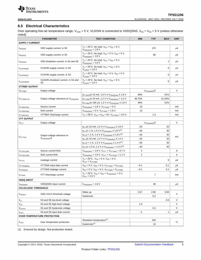
6.5 Electrical CharacteristicsOver operating free-air temperature range, VVDD = 5 V, VLDOIN is connected to VDDQSNS, VS3 = VS5 = 5 V (unless otherwisenoted)
PARAMETER TEST CONDITION MIN TYP MAX UNIT
SUPPLY CURRENT
IVDD(S0) VDD supply current, in S0 TA = 25°C, No load, VS3 = VS5 = 5 V,VVDDQSNS = 1.8 V 170 μA
IVDD(S3) VDD supply current, in S3 TA = 25°C, No load, VS3 = 0 V, VS5 = 5 V,VVDDQSNS = 1.8 V 80 μA
IVDDSDN VDD shutdown current, in S4 and S5 TA = 25°C, No load, VS3 = VS5 = 0 V,VVDDQSNS = 1.8 V 1 μA
IVLDOIN(S0) VLDOIN supply current, in S0 TA = 25°C, No load, VS3 = VS5 = 5 V,VLDION = 1.8 V 5 μA
IVLDOIN(s3) VLDOIN supply current, in S3 TA = 25°C, No load, VS3 = 0 V, VS5 = 5 V,VLDION = 1.8 V 5 μA
IVLDOINSDNVLDOIN shutdown current, in S4 andS5
TA = 25°C, No load, VS3 = VS5 = 0 V,VLDION = 1.8 V 5 μA
VTTREF OUTPUT
VVTTREF Output voltage VVDDQSNS/2 V
VVTTREFTOL Output voltage tolerance to VVDDQSNS
|IVTTREF|≤ 10 mA, 1.5 V ≤ VVDDQSNS ≤ 1.8 V 49% 51%
|IVTTREF|≤ 10 mA, 1.2 V ≤ VVDDQSNS < 1.5 V 48.75% 51.25%
|IVTTREF|≤ 100 μA, 1.2 V ≤ VVDDQSNS ≤ 1.8 V 49% 51%
IVTTREFSRC Source current VVDDQSNS = 1.8 V, VVTTREF = 0 V 10 mA
IVTTREFSNK Sink current VVDDQSNS = 0 V, VVTTREF = 1.8 V 10 mA
IVTTREFDIS VTTREF Discharge current TA = 25°C, VS3 = VS5 = 0V, VVTTREF = 0.5 V 1.3 mA
VTT OUTPUT
VVTT Output voltage VVDDQSNS/2 V
VVTTTOLOutput voltage tolerance toVVDDQSNS/2
|IVTT|≤ 10 mA, 1.4 V ≤ VVDDQSNS ≤ 1.8 V –20 20
mV
|IVTT|< 1 A, 1.4 V ≤ VVDDQSNS ≤ 1.8 V (1) –30 30
|IVTT| < 2 A, 1.4 V ≤ VVDDQSNS ≤ 1.8 V (1) –40 40
|IVTT|≤ 10 mA, 1.2 V ≤ VVDDQSNS ≤ 1.4 V –20 20
|IVTT| < 1 A, 1.2 V ≤ VVDDQSNS ≤ 1.4 V (1) –30 30
|IVTT|< 1.5 A, 1.2 V ≤ VVDDQSNS < 1.4 V (1) –40 40
IVTTOCLSRC Source current limit VVDDQSNS = 1.8 V, VVTT = VVTTSNS = 0.7 V 2 A
IVTTOCLSNK Sink current limit VVDDQSNS = 1.8 V, VVTT = VVTTSNS = 1.1 V 2 A
IVTTLK Leakage current TA = 25°C , VS3 = 0 V, VS5 = 5 V,VVTT = VVTTREF
5 μA
IVTTSNSBIAS VTTSNS input bias current VS3 = 5 V, VS5 = 5 V, VVTTSNS = VVTTREF –0.1 0.1 μA
IVTTSNSLK VTTSNS leakage current VS3 = 0 V, VS5 = 5 V, VVTTSNS = VVTTREF –0.1 0.1 μA
IVTTDIS VTT Discharge current TA = 25°C, VS3 = VS5 = VVDDQSNS = 0 V,VVTT = 0.5 V 7 mA
VDDQ INPUT
IVDDQSNS VDDQSNS input current VVDDQSNS = 1.8 V 30 μA
UVLO/LOGIC THRESHOLD
VVDDUV VDD UVLO threshold voltageWake up 2.67 2.90 3.00
VHysteresis 0.2
VLL S3 and S5 low-level voltage 0.5 V
VLH S3 and S5 high-level voltage 1.8 V
VLHYST S3 and S5 hysteresis voltage 0.3 V
ILHLK S3 and S5 input leak current –1 1 μA
OVER-TEMPERATURE PROTECTION
TOTP Over temperature protectionShutdown temperature (1) 150
°CHysteresis (1) 10
0.880
0.885
0.890
0.895
0.900
0.905
0.910
0.915
0.920
−10 −8 −6 −4 −2 0 2 4 6 8 10VTTREF Current (mA)
VT
TR
EF
Vol
tage
(V
)
TA = −40°C TA = 25°C TA = 85°C
VVDDQSNS = 1.8 V VVDD = 5 V
0.730
0.735
0.740
0.745
0.750
0.755
0.760
0.765
0.770
−10 −8 −6 −4 −2 0 2 4 6 8 10VTTREF Current (mA)
VT
TR
EF
Vol
tage
(V
)
TA = −40°C TA = 25°C TA = 85°C
VVDDQSNS = 1.5 V VVDD = 5 V
0
1
2
3
4
5
−40 −25 −10 5 20 35 50 65 80 95 110 125Junction Temperature (°C)
VLD
OIN
Sup
ply
Cur
rent
(µA
)
0
1
2
3
4
5
−40 −25 −10 5 20 35 50 65 80 95 110 125Junction Temperature (°C)
VLD
OIN
Shu
tdow
n C
urre
nt (
µA)
0
50
100
150
200
250
300
−40 −25 −10 5 20 35 50 65 80 95 110 125Junction Temperature (°C)
VD
D S
uppl
y C
urre
nt (
µA)
0
1
2
3
4
5
−40 −25 −10 5 20 35 50 65 80 95 110 125Junction Temperature (°C)
VD
D S
hutd
own
Cur
rent
(µA
)
6
TPS51206SLUSAH1E –MAY 2011–REVISED JULY 2018 www.ti.com
Product Folder Links: TPS51206
Submit Documentation Feedback Copyright © 2011–2018, Texas Instruments Incorporated
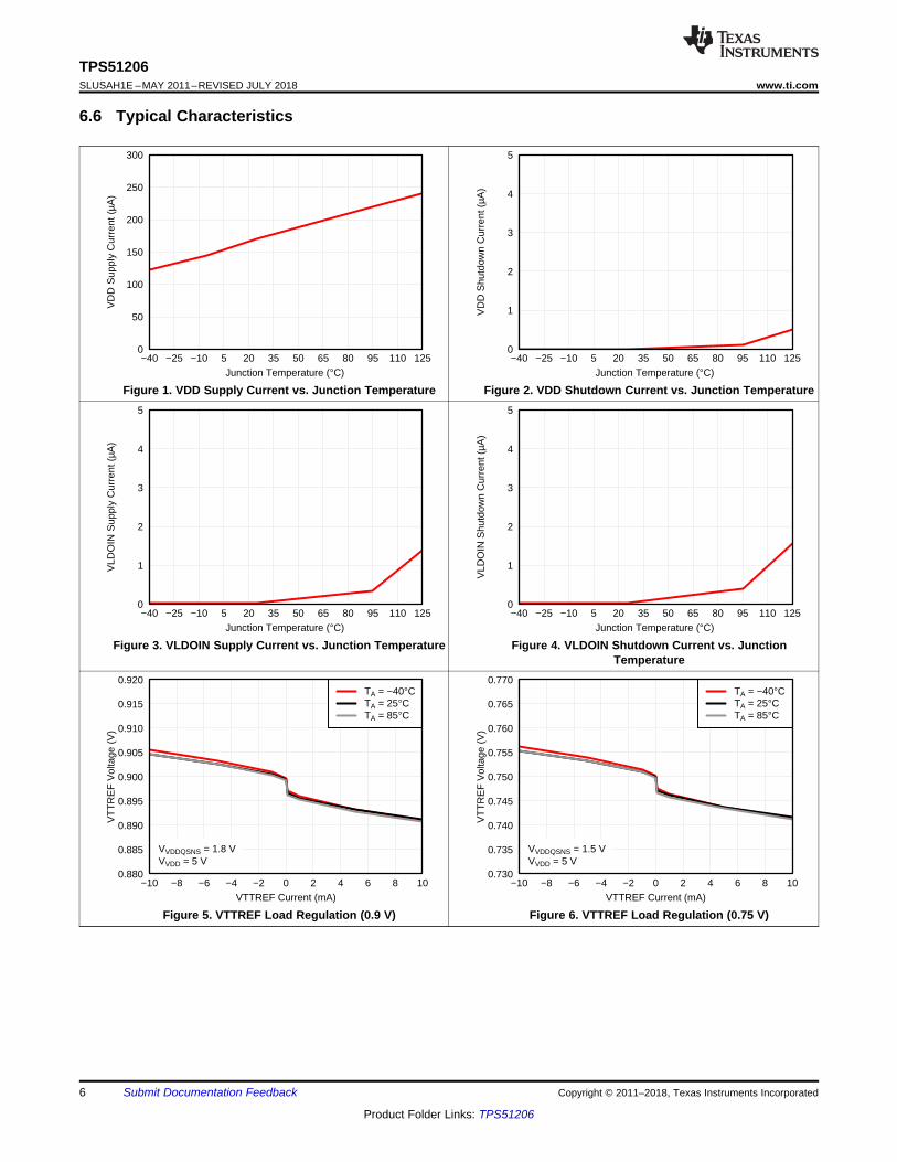
6.6 Typical Characteristics
Figure 1. VDD Supply Current vs. Junction Temperature Figure 2. VDD Shutdown Current vs. Junction Temperature
Figure 3. VLDOIN Supply Current vs. Junction Temperature Figure 4. VLDOIN Shutdown Current vs. JunctionTemperature
Figure 5. VTTREF Load Regulation (0.9 V) Figure 6. VTTREF Load Regulation (0.75 V)
0.625
0.635
0.645
0.655
0.665
0.675
0.685
0.695
0.705
0.715
0.725
−1.5 −1.0 −0.5 0.0 0.5 1.0 1.5VTT Current (A)
VT
T V
olta
ge (
V)
TA = −40°C TA = 25°C TA = 85°C
VVDDQSNS = 1.35 V VVDD = 5 V
0.550
0.560
0.570
0.580
0.590
0.600
0.610
0.620
0.630
0.640
0.650
−1.5 −1.0 −0.5 0.0 0.5 1.0 1.5VTT Current (A)
VT
T V
olta
ge (
V)
TA = −40°C TA = 25°C TA = 85°C
VVDDQSNS = 1.2 V VVDD = 5 V
0.850
0.860
0.870
0.880
0.890
0.900
0.910
0.920
0.930
0.940
0.950
−2.0 −1.5 −1.0 −0.5 0.0 0.5 1.0 1.5 2.0VTT Current (A)
VT
T V
olta
ge (
V)
TA = −40°C TA = 25°C TA = 85°C
VVDDQSNS = 1.8 V VVDD = 5 V
0.700
0.710
0.720
0.730
0.740
0.750
0.760
0.770
0.780
0.790
0.800
−2.0 −1.5 −1.0 −0.5 0.0 0.5 1.0 1.5 2.0VTT Current (A)
VT
T V
olta
ge (
V)
TA = −40°C TA = 25°C TA = 85°C
VVDDQSNS = 1.5 V VVDD = 5 V
0.660
0.665
0.670
0.675
0.680
0.685
0.690
−10 −8 −6 −4 −2 0 2 4 6 8 10VTTREF Current (mA)
VT
TR
EF
Vol
tage
(V
)
TA = −40°C TA = 25°C TA = 85°C
VVDDQSNS = 1.35 V VVDD = 5 V
0.585
0.590
0.595
0.600
0.605
0.610
0.615
−10 −8 −6 −4 −2 0 2 4 6 8 10VTTREF Current (mA)
VT
TR
EF
Vol
tage
(V
)
TA = −40°C TA = 25°C TA = 85°C
VVDDQSNS = 1.2 V VVDD = 5 V
7
TPS51206www.ti.com SLUSAH1E –MAY 2011–REVISED JULY 2018
Product Folder Links: TPS51206
Submit Documentation FeedbackCopyright © 2011–2018, Texas Instruments Incorporated
Typical Characteristics (continued)
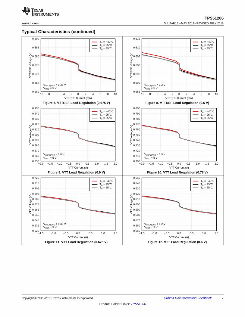
Figure 7. VTTREF Load Regulation (0.675 V) Figure 8. VTTREF Load Regulation (0.6 V)
Figure 9. VTT Load Regulation (0.9 V) Figure 10. VTT Load Regulation (0.75 V)
Figure 11. VTT Load Regulation (0.675 V) Figure 12. VTT Load Regulation (0.6 V)
1000 10000 100000 1000000 10000000−80
−60
−40
−20
0
20
40
60
80
−180
−135
−90
−45
0
45
90
135
180
Frequency (Hz)
Gai
n (d
B)
Pha
se (
°)
GainPhase
Sink: −1 AVVDD = 5 VVVDDQSNS = 1.5 V
1000 10000 100000 1000000 10000000−80
−60
−40
−20
0
20
40
60
80
−180
−135
−90
−45
0
45
90
135
180
Frequency (Hz)
Gai
n (d
B)
Pha
se (
°)
GainPhase
Source: +1 AVVDD = 5 VVVDDQSNS = 1.5 V
IVTT
(2 A/div)
VVTTREF
(10 mV/div) 0.675 V offset
Time (200 ms/div)
VVTT
(20 mV/div)
0.675 V offset
VVDDQSNS
(50 mV/div)
1.35 V offset
IVTT
(2 A/div)
VVTTREF
(10 mV/div) 0.6 V offset
Time (200 ms/div)
VVTT
(20 mV/div)
0.6 V offset
VVDDQSNS
(50 mV/div)
1.2 V offset
IVTT
(2 A/div)
VVTTREF
(10 mV/div) 0.9 V offset
Time (200 ms/div)
VVTT
(20 mV/div)
0.9 V offset
VVDDQSNS
(50 mV/div)
1.8 V offset
IVTT
(2 A/div)
VVTTREF
(10 mV/div) 0.75 V offset
Time (200 ms/div)
VVTT
(20 mV/div)
0.75 V offset
VVDDQSNS
(50 mV/div)
1.5 V offset
8
TPS51206SLUSAH1E –MAY 2011–REVISED JULY 2018 www.ti.com
Product Folder Links: TPS51206
Submit Documentation Feedback Copyright © 2011–2018, Texas Instruments Incorporated
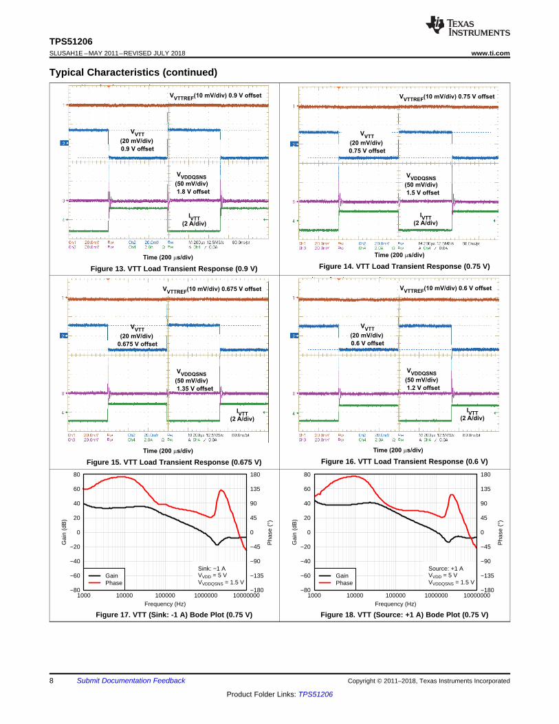
Typical Characteristics (continued)
Figure 13. VTT Load Transient Response (0.9 V) Figure 14. VTT Load Transient Response (0.75 V)
Figure 15. VTT Load Transient Response (0.675 V) Figure 16. VTT Load Transient Response (0.6 V)
Figure 17. VTT (Sink: -1 A) Bode Plot (0.75 V) Figure 18. VTT (Source: +1 A) Bode Plot (0.75 V)
IVTTREF
= 0 A
IVTT
= 0 A
S3/S5: High to LowV
VTTREF(500 mV/div)
VVTT
(500 mV/div)
VS5
(5 V/div)
VS3
(5 V/div)
Time (2 s/div)
0.00
0.05
0.10
0.15
0.20
0.25
0.30
0.0 0.5 1.0 1.5 2.0VTT Current (A)
VT
T D
ropo
ut V
olta
ge (
V)
VOUT = 0.900 V VOUT = 0.750 V VOUT = 0.675 V VOUT = 0.600 V
TA = 25°C VVDD = 5 V
VVTTREF
(500 mV/div)
Time (40 ms/div)
VVTT
(500 mV/div)
VS5
(5 V/div)
VS3
(5 V/div)
IVTTREF
= 0 A
S5: Low to High
IVTTREF
= 0 A
IVTT
= 0 A
S3: Low to High
VVTTREF
(500 mV/div)
VVTT
(500 mV/div)
VS5
(5 V/div)
VS3
(5 V/div)
Time (1 ms/div)
9
TPS51206www.ti.com SLUSAH1E –MAY 2011–REVISED JULY 2018
Product Folder Links: TPS51206
Submit Documentation FeedbackCopyright © 2011–2018, Texas Instruments Incorporated
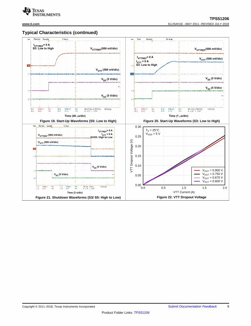
Typical Characteristics (continued)
Figure 19. Start-Up Waveforms (S5: Low to High) Figure 20. Start-Up Waveforms (S3: Low to High)
Figure 21. Shutdown Waveforms (S3/ S5: High to Low) Figure 22. VTT Dropout Voltage

1
2
7
9
VTT
VTTSNS
PGND
VTTREFVDDQSNS
VLDOIN
S3
S5
TPS51206
10VDD
GND
+
3
5
4
6
8
+
+
+
OTPGND
2.9V/2.7 V
+
+
GND
GND
OTP-OK
EN-VTTREF
EN-VTT
VTT Disharge
VTTREF Disharge
GND
Copyright © 2016, Texas Instruments Incorporated
10
TPS51206SLUSAH1E –MAY 2011–REVISED JULY 2018 www.ti.com
Product Folder Links: TPS51206
Submit Documentation Feedback Copyright © 2011–2018, Texas Instruments Incorporated
7 Detailed Description
7.1 OverviewThe TPS51206 device is a sink or source double date rate (DDR) termination regulator with VTTREF bufferedreference output.
7.2 Functional Block Diagram
7.3 Feature Description
7.3.1 VTT Sink and Source RegulatorThe TPS51206 device is a sink or source tracking termination regulator specifically designed for low inputvoltage, low cost, and low external component count systems where space is a key application parameter. Thedevice integrates a high-performance, low-dropout (LDO) linear regulator (VTT) that has ultimate fast response totrack ½ VDDQSNS within 40 mV at all conditions, and its current capability is 2 A for both sink and sourcedirections. A 10-µF (or greater) ceramic capacitor(s) need to be attached close to the VTT terminal for stableoperation. A grade of X5R or better is recommended. To achieve tight regulation with minimum effect of traceresistance, the remote sensing terminal, VTTSNS, should be connected to the positive terminal of the outputcapacitor(s) as a separate trace from the high current path from the VTT pin.
The device has a dedicated pin, VLDOIN, for VTT power supply to minimize the LDO power dissipation on userapplication. The minimum VLDOIN voltage is 0.4 V above the ½ VDDQSNS voltage.
7.3.2 VTTREFThe VTTREF pin includes 10 mA of sink or source current capability, and tracks ½ of VDDQSNS with ±1%accuracy. The VTTREF pin can not be open. A 0.22-µF ceramic capacitor needs to be attached close to theVTTREF terminal for stable operation; X5R or better grade is recommended.
UDG-11136
VDD
VLDOIN
S5
S3
VTTREF
VTT
VDDQSNS
11
TPS51206www.ti.com SLUSAH1E –MAY 2011–REVISED JULY 2018
Product Folder Links: TPS51206
Submit Documentation FeedbackCopyright © 2011–2018, Texas Instruments Incorporated
Feature Description (continued)7.3.3 VDD Undervoltage Lockout ProtectionThe TPS51206 device input voltage (VDD) includes undervoltage lockout protection (UVLO). When the VDD pinvoltage is lower than UVLO threshold voltage, VTT and VTTREF are shut off. This is non-latch protection.
7.3.4 VTT Current LimitThe TPS51206 device has VTT sink and source current limit capability. When the VTT current is higher than 2 A,the current is limited and VTT voltage is out of regulation. When the current is below 2 A, the VTT voltage is inregulation. This is non-latch protection.
7.3.5 Overtemperature ProtectionThis device features internal temperature monitoring. If the temperature exceeds the threshold value, VTT andVTTREF are shut off. This is a non-latch protection.
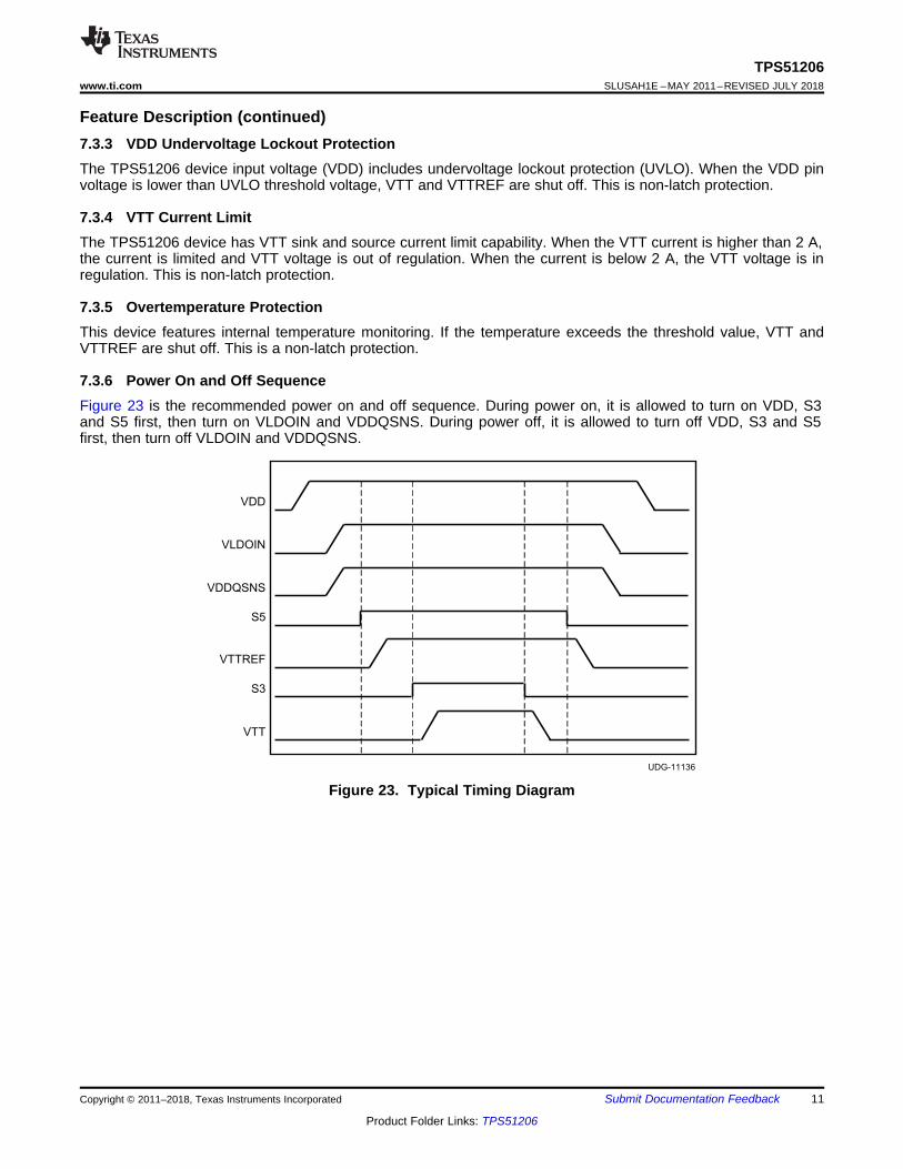
7.3.6 Power On and Off SequenceFigure 23 is the recommended power on and off sequence. During power on, it is allowed to turn on VDD, S3and S5 first, then turn on VLDOIN and VDDQSNS. During power off, it is allowed to turn off VDD, S3 and S5first, then turn off VLDOIN and VDDQSNS.
Figure 23. Typical Timing Diagram
12
TPS51206SLUSAH1E –MAY 2011–REVISED JULY 2018 www.ti.com
Product Folder Links: TPS51206
Submit Documentation Feedback Copyright © 2011–2018, Texas Instruments Incorporated
7.4 Device Functional Modes
7.4.1 Power State ControlThe TPS51206 device has two input pins, S3 and S5, to provide simple control of the power state. Table 1describes S3 and S5 terminal logic state and corresponding state of VTTREF and VTT outputs. VTT is turn-offand placed to high impedance (High-Z) state in S3. The VTT output is floated and does not sink or sourcecurrent in this state. When both S5 and S3 pins are LOW, the power state is set to S4 and S5 . In S4 and S5state, all the outputs are turn-off and discharged to GND.
Table 1. S3 and S5 Control TableSTATE S3 S5 VTTREF VTT
S0 HI HI ON ONS3 LO HI ON OFF(High-Z)
S4 and S5 LO LO OFF(Discharge) OFF(Discharge)
1
2
7
9
3
5
4
6
VTT
VTTSNS
PGND
VTTREF
VDDQSNS
VLDOIN
S3
S5
TPS51206
10 VDD 8GND
C310 PF
PowerPad
VTT
VTTREF
C40.22 PF
C20.1 PF
C110 PF
VDDQ
S3_SLP
S5_SLP
5 V or 3.3 V
GND
Copyright © 2016, Texas Instruments Incorporated
13
TPS51206www.ti.com SLUSAH1E –MAY 2011–REVISED JULY 2018
Product Folder Links: TPS51206
Submit Documentation FeedbackCopyright © 2011–2018, Texas Instruments Incorporated
8 Application and Implementation
NOTEInformation in the following applications sections is not part of the TI componentspecification, and TI does not warrant its accuracy or completeness. TI’s customers areresponsible for determining suitability of components for their purposes. Customers shouldvalidate and test their design implementation to confirm system functionality.
8.1 Application InformationThe TPS51206 device is typically used as a sink and source tracking termination regulator which converts avoltage from VTT+0.4 V to 3.5 V
8.2 Typical Applications
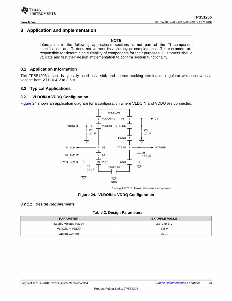
8.2.1 VLDOIN = VDDQ ConfigurationFigure 24 shows an application diagram for a configuration where VLDOIN and VDDQ are connected.
Figure 24. VLDOIN = VDDQ Configuration
8.2.1.1 Design Requirements
Table 2. Design ParametersPARAMETER EXAMPLE VALUE
Supply Voltage (VDD) 3.3 V or 5 VVLDOIN = VDDQ 1.5 V
Output Current ±2 A
3
5
4
VTT
VTTSNS
PGND
TPS51206
C3
10 mF
VTT
UDG-11137
CC
RC
14
TPS51206SLUSAH1E –MAY 2011–REVISED JULY 2018 www.ti.com
Product Folder Links: TPS51206
Submit Documentation Feedback Copyright © 2011–2018, Texas Instruments Incorporated
8.2.1.2 Detailed Design Procedure
Table 3. VLDOIN = VDDQ Configuration ComponentsREFERENCEDESIGNATOR SPECIFICATION MANUFACTURER PART
NUMBERC1, C3 10 µF, 6.3 V, X5R, 1608 (0603) Taiyo Yuden JMK107BJ106MAC2 0.1 µF, 6.3 V, X5R, 1005 (0402) Taiyo Yuden JWK105BJ104MPC4 0.22 µF, 6.3 V, X5R, 1005 (0402) Taiyo Yuden JMK105BJ224KV
8.2.1.2.1 VDD Capacitor
Add a ceramic capacitor, with a value 0.1 µF (or greater) and X5R grade (or better), placed close to the VDDterminal, to stabilize the bias supply voltage from any parasitic impedance from the power supply rail.
8.2.1.2.2 VLDOIN Capacitor
Depending on the trace impedance between the VLDOIN bulk power supply to the device, a transient increase ofsource current is supplied mostly by the charge from the VLDOIN input capacitor. Use a 10-µF (or greater) andX5R grade (or better) ceramic capacitor to supply this transient charge.
8.2.1.2.3 VTTREF Capacitor
Add a ceramic capacitor, with a value 0.22 µF and X5R grade (or better), placed close to the VTTREF terminalfor stable operation.
8.2.1.2.4 VTT Capacitor
For stable operation, a 10-µF (or greater) and X5R (or better) grade ceramic capacitor(s) need to be attachedclose to the VTT terminal. This capacitor is recommended to minimize any additional equivalent series resistance(ESR) and/or equivalent series inductance (ESL) of ground trace between the PGND terminal and the VTTcapacitor(s).
8.2.1.2.5 VTTSNS Connection
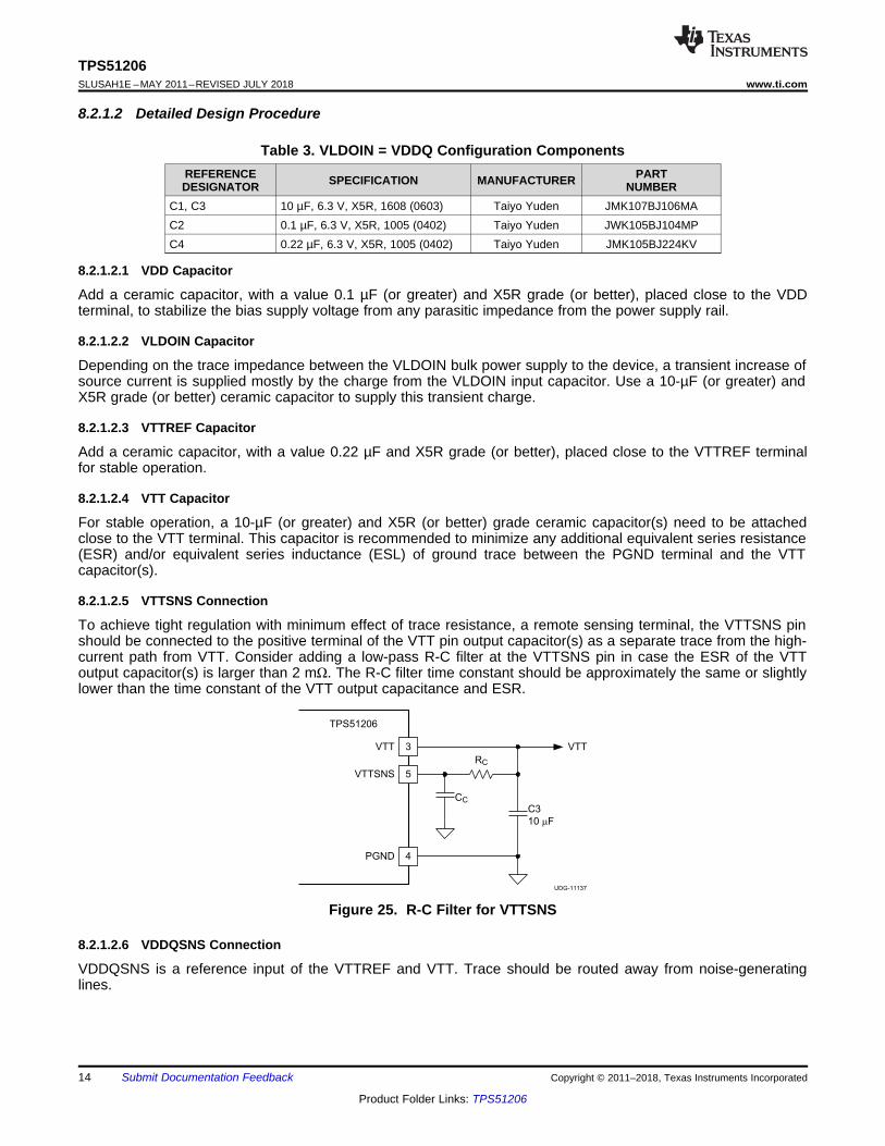
To achieve tight regulation with minimum effect of trace resistance, a remote sensing terminal, the VTTSNS pinshould be connected to the positive terminal of the VTT pin output capacitor(s) as a separate trace from the high-current path from VTT. Consider adding a low-pass R-C filter at the VTTSNS pin in case the ESR of the VTToutput capacitor(s) is larger than 2 mΩ. The R-C filter time constant should be approximately the same or slightlylower than the time constant of the VTT output capacitance and ESR.
Figure 25. R-C Filter for VTTSNS
8.2.1.2.6 VDDQSNS Connection
VDDQSNS is a reference input of the VTTREF and VTT. Trace should be routed away from noise-generatinglines.
1
2
7
9
3
5
4
6
VTT
VTTSNS
PGND
VTTREF
VDDQSNS
VLDOIN
S3
S5
TPS51206
10 VDD 8GND
C310 PF
PowerPad
VTT
VTTREF
C40.22 PF
C20.1 PF
C110 PF
VTT Power
S3_SLP
S5_SLP
5 V or 3.3 V Supply
GND
VDDQ Sense
Copyright © 2016, Texas Instruments Incorporated
IVTT
(2 A/div)
VVTTREF
(10 mV/div) 0.75 V offset
Time (200 ms/div)
VVTT
(20 mV/div)
0.75 V offset
VVDDQSNS
(50 mV/div)
1.5 V offset
15
TPS51206www.ti.com SLUSAH1E –MAY 2011–REVISED JULY 2018
Product Folder Links: TPS51206
Submit Documentation FeedbackCopyright © 2011–2018, Texas Instruments Incorporated
8.2.1.3 Application Curves
Figure 26. VTT Load Transient Response (0.75 V)
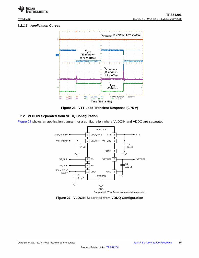
8.2.2 VLDOIN Separated from VDDQ ConfigurationFigure 27 shows an application diagram for a configuration where VLDOIN and VDDQ are separated.
Figure 27. VLDOIN Separated from VDDQ Configuration
IVTTREF
= 0 A
IVTT
= 0 A
S3: Low to High
VVTTREF
(500 mV/div)
VVTT
(500 mV/div)
VS5
(5 V/div)
VS3
(5 V/div)
Time (1 ms/div)
IVTTREF
= 0 A
IVTT
= 0 A
S3/S5: High to LowV
VTTREF(500 mV/div)
VVTT
(500 mV/div)
VS5
(5 V/div)
VS3
(5 V/div)
Time (2 s/div)
16
TPS51206SLUSAH1E –MAY 2011–REVISED JULY 2018 www.ti.com
Product Folder Links: TPS51206
Submit Documentation Feedback Copyright © 2011–2018, Texas Instruments Incorporated
8.2.2.1 Design Requirements
Table 4. Design ParametersPARAMETER EXAMPLE VALUE
Supply Voltage (VDD) 3.3 V or 5 V
VLDOIN = VDDQ 1.5 V
Output Current ±2 A
8.2.2.2 Detailed Design Procedure
Table 5. VLDOIN Separated from VDDQ Configuration ComponentsREFERENCEDESIGNATOR SPECIFICATION MANUFACTURER PART
NUMBERC1, C3 10 µF, 6.3V, X5R, 1608 (0603) Taiyo Yuden JMK107BJ106MAC2 0.1 µF, 6.3V, X5R, 1005 (0402) Taiyo Yuden JWK105BJ104MPC3 10 µF, 6.3V, X5R, 1608 (0603) Taiyo Yuden JMK107BJ106MAC4 0.22 µF, 6.3V, X5R, 1005 (0402) Taiyo Yuden JMK105BJ224KV
8.2.2.3 Application Curves
Figure 28. Start-Up Waveforms (S3: Low to High) Figure 29. Shutdown Waveforms (S3 / S5: High to Low)
17
TPS51206www.ti.com SLUSAH1E –MAY 2011–REVISED JULY 2018
Product Folder Links: TPS51206
Submit Documentation FeedbackCopyright © 2011–2018, Texas Instruments Incorporated
9 Power Supply RecommendationsTPS51206 device is designed for a sink / source double date rate (DDR) termination regulator with VTTREFbuffered reference output. Supply input voltage (VDD) supports 3.3-V rail and 5-V rail; VLDOIN input voltagesupports VTT+0.4 V to 3.5 V.
10 Layout
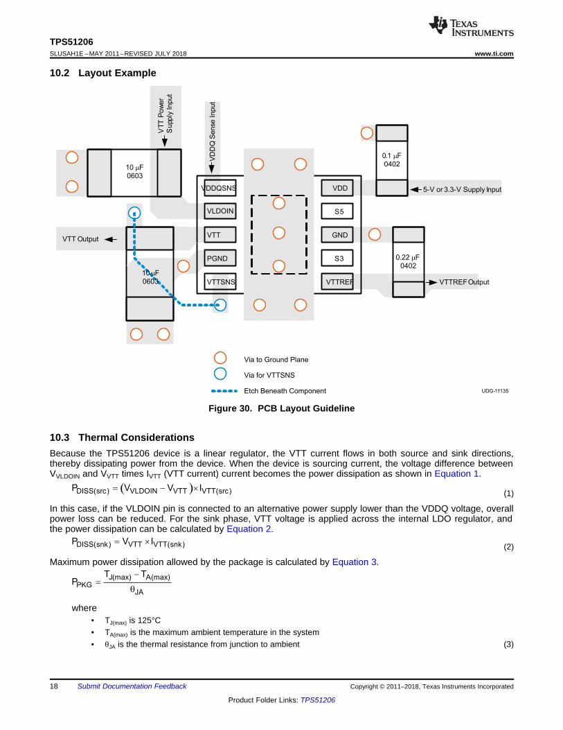
10.1 Layout GuidelinesConsider the following before beginning a TPS51206 device layout design.• The input bypass capacitor for VLDOIN should be placed as close as possible to the terminal with short and
wide connections.• The output capacitor for VTT should be placed close to the terminals (VTT and PGND) with short and wide
connection in order to avoid additional ESR and/or ESL trace inductance.• VTTSNS should be connected to the positive node of VTT output capacitor(s) as a separate trace from the
high current VTT power trace. In addition, VTTSNS trace should be routed away from high current trace, onthe separate layer is recommended. This configuration is strongly recommended to avoid additional ESRand/or ESL. If sensing the voltage at the point of the load is required, it is recommended to attach the outputcapacitor(s) at that point. In addition, it is recommended to minimize any additional ESR and/or ESL of groundtrace between the GND pin and the VTT capacitor(s).
• The GND pin (and the negative node of the VTTREF output capacitor) and PGND pins (and the negativenode of the VTT output capacitor) should be connected to the internal system ground planes (for better result,use at least two internal ground planes) with multiple vias. Use as many vias as possible to reduce theimpedance between GND pin or PGND pin and the system ground plane.
• In order to effectively remove heat from the package, properly prepare the thermal land. Apply solder directlyto the package thermal pad. The wide traces of the component and the side copper connected to the thermalland pad help to dissipate heat. Numerous vias 0.33 mm in diameter connected from the thermal land to theinternal/solder side ground plane(s) should also be used to help dissipation. Consult the TPS51206-EVMUser's Guide for more detailed layout recommendations.
-=
q
J(max) A(max)PKG
JA
T TP
= ´DISS(snk) VTT VTT(snk)P V I
( )= - ´DISS(src) VLDOIN VTT VTT(src)P V V I
UDG-11135
0.22 mF
0402
0.1 mF
0402
VLDOIN
VTT
PGND
VTTSNS
VDD
S5
GND
S3
VTTREF
VDDQSNS
Via to Ground Plane
Via for VTTSNS
VTTREFOutput
5-V or 3.3-V Supply Input
VTT Output
VD
DQ
Sense
Input
VTT
Pow
er
Supp
lyIn
put
Etch Beneath Component
10 mF
0603
10 mF
0603
18
TPS51206SLUSAH1E –MAY 2011–REVISED JULY 2018 www.ti.com
Product Folder Links: TPS51206
Submit Documentation Feedback Copyright © 2011–2018, Texas Instruments Incorporated
10.2 Layout Example
Figure 30. PCB Layout Guideline
10.3 Thermal ConsiderationsBecause the TPS51206 device is a linear regulator, the VTT current flows in both source and sink directions,thereby dissipating power from the device. When the device is sourcing current, the voltage difference betweenVVLDOIN and VVTT times IVTT (VTT current) current becomes the power dissipation as shown in Equation 1.
(1)
In this case, if the VLDOIN pin is connected to an alternative power supply lower than the VDDQ voltage, overallpower loss can be reduced. For the sink phase, VTT voltage is applied across the internal LDO regulator, andthe power dissipation can be calculated by Equation 2.
(2)
Maximum power dissipation allowed by the package is calculated by Equation 3.
where• TJ(max) is 125°C• TA(max) is the maximum ambient temperature in the system• θJA is the thermal resistance from junction to ambient (3)
19
TPS51206www.ti.com SLUSAH1E –MAY 2011–REVISED JULY 2018
Product Folder Links: TPS51206
Submit Documentation FeedbackCopyright © 2011–2018, Texas Instruments Incorporated
11 Device and Documentation Support
11.1 Device Support
11.1.1 Third-Party Products DisclaimerTI'S PUBLICATION OF INFORMATION REGARDING THIRD-PARTY PRODUCTS OR SERVICES DOES NOTCONSTITUTE AN ENDORSEMENT REGARDING THE SUITABILITY OF SUCH PRODUCTS OR SERVICESOR A WARRANTY, REPRESENTATION OR ENDORSEMENT OF SUCH PRODUCTS OR SERVICES, EITHERALONE OR IN COMBINATION WITH ANY TI PRODUCT OR SERVICE.
11.2 Receiving Notification of Documentation UpdatesTo receive notification of documentation updates, navigate to the device product folder on ti.com. In the upperright corner, click on Alert me to register and receive a weekly digest of any product information that haschanged. For change details, review the revision history included in any revised document.
11.3 Community Resources
The following links connect to TI community resources. Linked contents are provided "AS IS" by the respectivecontributors. They do not constitute TI specifications and do not necessarily reflect TI's views; see TI's Terms ofUse.
TI E2E™ Online Community TI's Engineer-to-Engineer (E2E) Community. Created to foster collaborationamong engineers. At e2e.ti.com, you can ask questions, share knowledge, explore ideas and helpsolve problems with fellow engineers.
Design Support TI's Design Support Quickly find helpful E2E forums along with design support tools andcontact information for technical support.
11.4 TrademarksPowerPAD, E2E are trademarks of Texas Instruments.All other trademarks are the property of their respective owners.
11.5 Electrostatic Discharge CautionThese devices have limited built-in ESD protection. The leads should be shorted together or the device placed in conductive foamduring storage or handling to prevent electrostatic damage to the MOS gates.
11.6 GlossarySLYZ022 — TI Glossary.
This glossary lists and explains terms, acronyms, and definitions.
12 Mechanical, Packaging, and Orderable InformationThe following pages include mechanical, packaging, and orderable information. This information is the mostcurrent data available for the designated devices. This data is subject to change without notice and revision ofthis document. For browser-based versions of this data sheet, refer to the left-hand navigation.
PACKAGE OPTION ADDENDUM
www.ti.com 6-Jul-2018
Addendum-Page 1
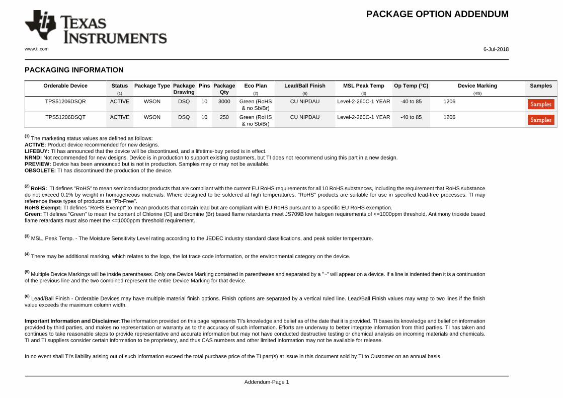
PACKAGING INFORMATION
Orderable Device Status(1)
Package Type PackageDrawing
Pins PackageQty
Eco Plan(2)
Lead/Ball Finish(6)
MSL Peak Temp(3)
Op Temp (°C) Device Marking(4/5)
Samples
TPS51206DSQR ACTIVE WSON DSQ 10 3000 Green (RoHS& no Sb/Br)
CU NIPDAU Level-2-260C-1 YEAR -40 to 85 1206
TPS51206DSQT ACTIVE WSON DSQ 10 250 Green (RoHS& no Sb/Br)
CU NIPDAU Level-2-260C-1 YEAR -40 to 85 1206
(1) The marketing status values are defined as follows:ACTIVE: Product device recommended for new designs.LIFEBUY: TI has announced that the device will be discontinued, and a lifetime-buy period is in effect.NRND: Not recommended for new designs. Device is in production to support existing customers, but TI does not recommend using this part in a new design.PREVIEW: Device has been announced but is not in production. Samples may or may not be available.OBSOLETE: TI has discontinued the production of the device.
(2) RoHS: TI defines "RoHS" to mean semiconductor products that are compliant with the current EU RoHS requirements for all 10 RoHS substances, including the requirement that RoHS substancedo not exceed 0.1% by weight in homogeneous materials. Where designed to be soldered at high temperatures, "RoHS" products are suitable for use in specified lead-free processes. TI mayreference these types of products as "Pb-Free".RoHS Exempt: TI defines "RoHS Exempt" to mean products that contain lead but are compliant with EU RoHS pursuant to a specific EU RoHS exemption.Green: TI defines "Green" to mean the content of Chlorine (Cl) and Bromine (Br) based flame retardants meet JS709B low halogen requirements of <=1000ppm threshold. Antimony trioxide basedflame retardants must also meet the <=1000ppm threshold requirement.
(3) MSL, Peak Temp. - The Moisture Sensitivity Level rating according to the JEDEC industry standard classifications, and peak solder temperature.
(4) There may be additional marking, which relates to the logo, the lot trace code information, or the environmental category on the device.
(5) Multiple Device Markings will be inside parentheses. Only one Device Marking contained in parentheses and separated by a "~" will appear on a device. If a line is indented then it is a continuationof the previous line and the two combined represent the entire Device Marking for that device.
(6) Lead/Ball Finish - Orderable Devices may have multiple material finish options. Finish options are separated by a vertical ruled line. Lead/Ball Finish values may wrap to two lines if the finishvalue exceeds the maximum column width.
Important Information and Disclaimer:The information provided on this page represents TI's knowledge and belief as of the date that it is provided. TI bases its knowledge and belief on informationprovided by third parties, and makes no representation or warranty as to the accuracy of such information. Efforts are underway to better integrate information from third parties. TI has taken andcontinues to take reasonable steps to provide representative and accurate information but may not have conducted destructive testing or chemical analysis on incoming materials and chemicals.TI and TI suppliers consider certain information to be proprietary, and thus CAS numbers and other limited information may not be available for release.
In no event shall TI's liability arising out of such information exceed the total purchase price of the TI part(s) at issue in this document sold by TI to Customer on an annual basis.
PACKAGE OPTION ADDENDUM
www.ti.com 6-Jul-2018
Addendum-Page 2
TAPE AND REEL INFORMATION
*All dimensions are nominal
Device PackageType
PackageDrawing
Pins SPQ ReelDiameter
(mm)
ReelWidth
W1 (mm)
A0(mm)
B0(mm)
K0(mm)
P1(mm)
W(mm)
Pin1Quadrant
TPS51206DSQR WSON DSQ 10 3000 180.0 8.4 2.3 2.3 1.15 4.0 8.0 Q2
TPS51206DSQT WSON DSQ 10 250 180.0 8.4 2.3 2.3 1.15 4.0 8.0 Q2
PACKAGE MATERIALS INFORMATION
www.ti.com 6-Jul-2018
Pack Materials-Page 1
*All dimensions are nominal
Device Package Type Package Drawing Pins SPQ Length (mm) Width (mm) Height (mm)
TPS51206DSQR WSON DSQ 10 3000 210.0 185.0 35.0
TPS51206DSQT WSON DSQ 10 250 210.0 185.0 35.0
PACKAGE MATERIALS INFORMATION
www.ti.com 6-Jul-2018
Pack Materials-Page 2
IMPORTANT NOTICE
Texas Instruments Incorporated (TI) reserves the right to make corrections, enhancements, improvements and other changes to itssemiconductor products and services per JESD46, latest issue, and to discontinue any product or service per JESD48, latest issue. Buyersshould obtain the latest relevant information before placing orders and should verify that such information is current and complete.TI’s published terms of sale for semiconductor products (http://www.ti.com/sc/docs/stdterms.htm) apply to the sale of packaged integratedcircuit products that TI has qualified and released to market. Additional terms may apply to the use or sale of other types of TI products andservices.Reproduction of significant portions of TI information in TI data sheets is permissible only if reproduction is without alteration and isaccompanied by all associated warranties, conditions, limitations, and notices. TI is not responsible or liable for such reproduceddocumentation. Information of third parties may be subject to additional restrictions. Resale of TI products or services with statementsdifferent from or beyond the parameters stated by TI for that product or service voids all express and any implied warranties for theassociated TI product or service and is an unfair and deceptive business practice. TI is not responsible or liable for any such statements.Buyers and others who are developing systems that incorporate TI products (collectively, “Designers”) understand and agree that Designersremain responsible for using their independent analysis, evaluation and judgment in designing their applications and that Designers havefull and exclusive responsibility to assure the safety of Designers' applications and compliance of their applications (and of all TI productsused in or for Designers’ applications) with all applicable regulations, laws and other applicable requirements. Designer represents that, withrespect to their applications, Designer has all the necessary expertise to create and implement safeguards that (1) anticipate dangerousconsequences of failures, (2) monitor failures and their consequences, and (3) lessen the likelihood of failures that might cause harm andtake appropriate actions. Designer agrees that prior to using or distributing any applications that include TI products, Designer willthoroughly test such applications and the functionality of such TI products as used in such applications.TI’s provision of technical, application or other design advice, quality characterization, reliability data or other services or information,including, but not limited to, reference designs and materials relating to evaluation modules, (collectively, “TI Resources”) are intended toassist designers who are developing applications that incorporate TI products; by downloading, accessing or using TI Resources in anyway, Designer (individually or, if Designer is acting on behalf of a company, Designer’s company) agrees to use any particular TI Resourcesolely for this purpose and subject to the terms of this Notice.TI’s provision of TI Resources does not expand or otherwise alter TI’s applicable published warranties or warranty disclaimers for TIproducts, and no additional obligations or liabilities arise from TI providing such TI Resources. TI reserves the right to make corrections,enhancements, improvements and other changes to its TI Resources. TI has not conducted any testing other than that specificallydescribed in the published documentation for a particular TI Resource.Designer is authorized to use, copy and modify any individual TI Resource only in connection with the development of applications thatinclude the TI product(s) identified in such TI Resource. NO OTHER LICENSE, EXPRESS OR IMPLIED, BY ESTOPPEL OR OTHERWISETO ANY OTHER TI INTELLECTUAL PROPERTY RIGHT, AND NO LICENSE TO ANY TECHNOLOGY OR INTELLECTUAL PROPERTYRIGHT OF TI OR ANY THIRD PARTY IS GRANTED HEREIN, including but not limited to any patent right, copyright, mask work right, orother intellectual property right relating to any combination, machine, or process in which TI products or services are used. Informationregarding or referencing third-party products or services does not constitute a license to use such products or services, or a warranty orendorsement thereof. Use of TI Resources may require a license from a third party under the patents or other intellectual property of thethird party, or a license from TI under the patents or other intellectual property of TI.TI RESOURCES ARE PROVIDED “AS IS” AND WITH ALL FAULTS. TI DISCLAIMS ALL OTHER WARRANTIES ORREPRESENTATIONS, EXPRESS OR IMPLIED, REGARDING RESOURCES OR USE THEREOF, INCLUDING BUT NOT LIMITED TOACCURACY OR COMPLETENESS, TITLE, ANY EPIDEMIC FAILURE WARRANTY AND ANY IMPLIED WARRANTIES OFMERCHANTABILITY, FITNESS FOR A PARTICULAR PURPOSE, AND NON-INFRINGEMENT OF ANY THIRD PARTY INTELLECTUALPROPERTY RIGHTS. TI SHALL NOT BE LIABLE FOR AND SHALL NOT DEFEND OR INDEMNIFY DESIGNER AGAINST ANY CLAIM,INCLUDING BUT NOT LIMITED TO ANY INFRINGEMENT CLAIM THAT RELATES TO OR IS BASED ON ANY COMBINATION OFPRODUCTS EVEN IF DESCRIBED IN TI RESOURCES OR OTHERWISE. IN NO EVENT SHALL TI BE LIABLE FOR ANY ACTUAL,DIRECT, SPECIAL, COLLATERAL, INDIRECT, PUNITIVE, INCIDENTAL, CONSEQUENTIAL OR EXEMPLARY DAMAGES INCONNECTION WITH OR ARISING OUT OF TI RESOURCES OR USE THEREOF, AND REGARDLESS OF WHETHER TI HAS BEENADVISED OF THE POSSIBILITY OF SUCH DAMAGES.Unless TI has explicitly designated an individual product as meeting the requirements of a particular industry standard (e.g., ISO/TS 16949and ISO 26262), TI is not responsible for any failure to meet such industry standard requirements.Where TI specifically promotes products as facilitating functional safety or as compliant with industry functional safety standards, suchproducts are intended to help enable customers to design and create their own applications that meet applicable functional safety standardsand requirements. Using products in an application does not by itself establish any safety features in the application. Designers mustensure compliance with safety-related requirements and standards applicable to their applications. Designer may not use any TI products inlife-critical medical equipment unless authorized officers of the parties have executed a special contract specifically governing such use.Life-critical medical equipment is medical equipment where failure of such equipment would cause serious bodily injury or death (e.g., lifesupport, pacemakers, defibrillators, heart pumps, neurostimulators, and implantables). Such equipment includes, without limitation, allmedical devices identified by the U.S. Food and Drug Administration as Class III devices and equivalent classifications outside the U.S.TI may expressly designate certain products as completing a particular qualification (e.g., Q100, Military Grade, or Enhanced Product).Designers agree that it has the necessary expertise to select the product with the appropriate qualification designation for their applicationsand that proper product selection is at Designers’ own risk. Designers are solely responsible for compliance with all legal and regulatoryrequirements in connection with such selection.Designer will fully indemnify TI and its representatives against any damages, costs, losses, and/or liabilities arising out of Designer’s non-compliance with the terms and provisions of this Notice.
Mailing Address: Texas Instruments, Post Office Box 655303, Dallas, Texas 75265Copyright © 2018, Texas Instruments Incorporated