ddr basics, register configurations & pitfalls · 2016-03-12 · write latency 1 read latency -...
TRANSCRIPT

TM
Freescale™ and the Freescale logo are trademarks of Freescale Semiconductor, Inc. All other product or service names are the property of their respective owners. © Freescale Semiconductor, Inc. 2009. 1
DDR Basics, Register Configurations & Pitfalls
July, 2009
Mazyar Razzaz, Applications Engineer

TMFreescale Semiconductor Confidential and Proprietary Information. Freescale™ and the Freescale logo are trademarksof Freescale Semiconductor, Inc. All other product or service names are the property of their respective owners. © Freescale Semiconductor, Inc. 2009. 2
Agenda
►Basic DDR SDRAM• Memory Organization & Operation• Read and write timing
►Power QUICC DDR Controllers• Features & Capabilities
►Power QUICC DDR Controllers• Initialization & Register Configurations
►Power QUICC DDR Controllers• Pitfalls / Debug Tips
TMFreescale™ and the Freescale logo are trademarks of Freescale Semiconductor, Inc. All other product or service names are the property of their respective owners. © Freescale Semiconductor, Inc. 2009. 3
Basic DDR SDRAMMemory Organization & Operation
TMFreescale Semiconductor Confidential and Proprietary Information. Freescale™ and the Freescale logo are trademarksof Freescale Semiconductor, Inc. All other product or service names are the property of their respective owners. © Freescale Semiconductor, Inc. 2009. 4
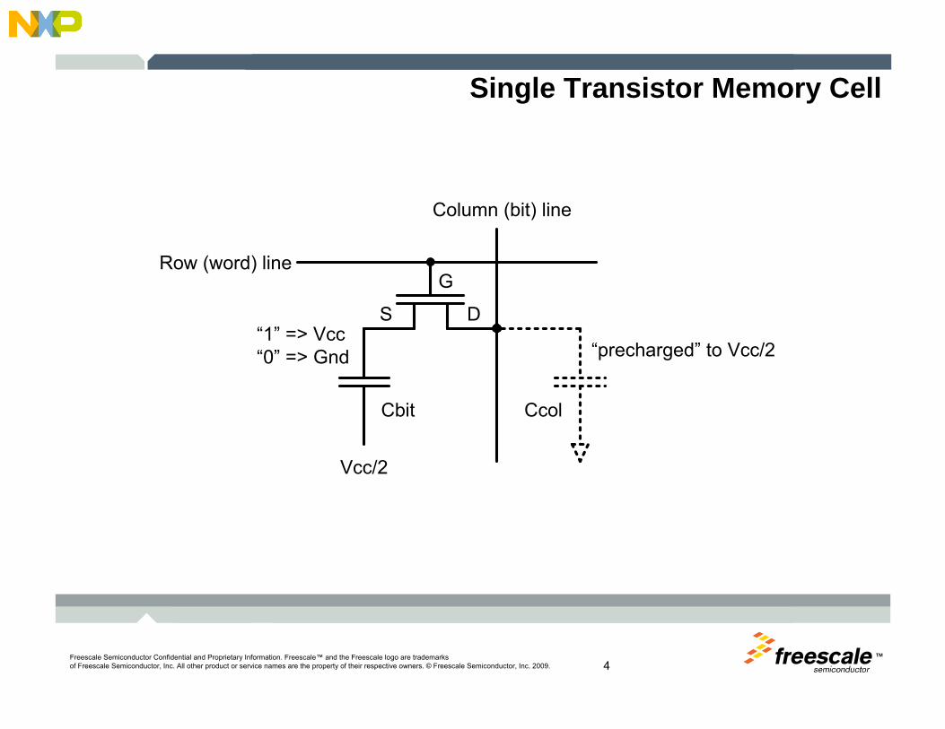
Single Transistor Memory Cell
S D
G
Cbit Ccol
Row (word) line
Column (bit) line
“1” => Vcc“0” => Gnd
Vcc/2
“precharged” to Vcc/2

TMFreescale Semiconductor Confidential and Proprietary Information. Freescale™ and the Freescale logo are trademarksof Freescale Semiconductor, Inc. All other product or service names are the property of their respective owners. © Freescale Semiconductor, Inc. 2009. 5
Single Transistor Memory Cell
S D
G
Cbit Ccol
Row (word) line
Column (bit) line
“1” => Vcc“0” => Gnd
Vcc/2
“precharged” to Vcc/2
Storage Capacitor

TMFreescale Semiconductor Confidential and Proprietary Information. Freescale™ and the Freescale logo are trademarksof Freescale Semiconductor, Inc. All other product or service names are the property of their respective owners. © Freescale Semiconductor, Inc. 2009. 6
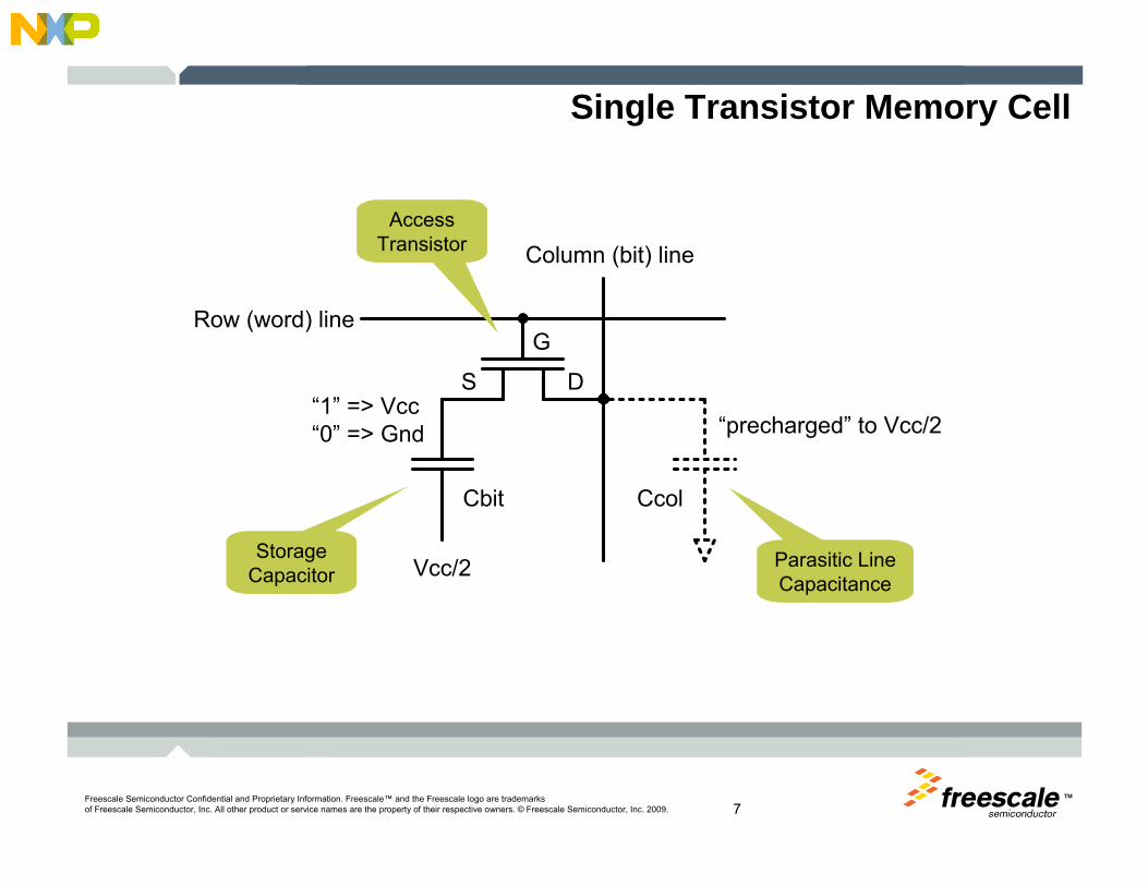
Single Transistor Memory Cell
S D
G
Cbit Ccol
Row (word) line
Column (bit) line
“1” => Vcc“0” => Gnd
Vcc/2
“precharged” to Vcc/2
Storage Capacitor
Access Transistor
TMFreescale Semiconductor Confidential and Proprietary Information. Freescale™ and the Freescale logo are trademarksof Freescale Semiconductor, Inc. All other product or service names are the property of their respective owners. © Freescale Semiconductor, Inc. 2009. 7
Single Transistor Memory Cell
S D
G
Cbit Ccol
Row (word) line
Column (bit) line
“1” => Vcc“0” => Gnd
Vcc/2
“precharged” to Vcc/2
Storage Capacitor
Parasitic Line Capacitance
Access Transistor

TMFreescale Semiconductor Confidential and Proprietary Information. Freescale™ and the Freescale logo are trademarksof Freescale Semiconductor, Inc. All other product or service names are the property of their respective owners. © Freescale Semiconductor, Inc. 2009. 8
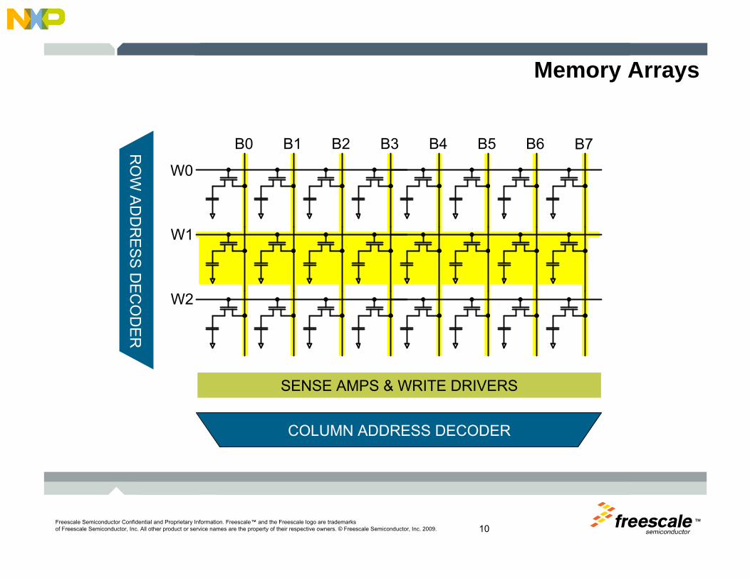
Memory Arrays
RO
W AD
DR
ESS DEC
OD
ER
SENSE AMPS & WRITE DRIVERS
COLUMN ADDRESS DECODER
W0
B0
W1
W2
B1 B2 B3 B4 B5 B6 B7

TMFreescale Semiconductor Confidential and Proprietary Information. Freescale™ and the Freescale logo are trademarksof Freescale Semiconductor, Inc. All other product or service names are the property of their respective owners. © Freescale Semiconductor, Inc. 2009. 9
Memory Arrays
RO
W AD
DR
ESS DEC
OD
ER
SENSE AMPS & WRITE DRIVERS
COLUMN ADDRESS DECODER
W0
B0
W1
W2
B1 B2 B3 B4 B5 B6 B7
TMFreescale Semiconductor Confidential and Proprietary Information. Freescale™ and the Freescale logo are trademarksof Freescale Semiconductor, Inc. All other product or service names are the property of their respective owners. © Freescale Semiconductor, Inc. 2009. 10
Memory Arrays
RO
W AD
DR
ESS DEC
OD
ER
SENSE AMPS & WRITE DRIVERS
COLUMN ADDRESS DECODER
W0
B0
W1
W2
B1 B2 B3 B4 B5 B6 B7

TMFreescale Semiconductor Confidential and Proprietary Information. Freescale™ and the Freescale logo are trademarksof Freescale Semiconductor, Inc. All other product or service names are the property of their respective owners. © Freescale Semiconductor, Inc. 2009. 11
Internal Memory Banks
►Multiple arrays organized into banks►Multiple banks per memory device
• DDR1 – 4 banks, 2 bank address (BA) bits• DDR2 & DDR3– 4 or 8 banks, 2 or 3 bank address (BA) bits• Can have one active row in each bank at any given time
►Concurrency• Can be opening or precharging a row in one bank while accessing another bank
►May be referred to as “internal”, “logical” or “sub-” banks
Bank 0Row 0Row 1
Row 3Row 2
Bank 1 Bank 2 Bank 3
RowBuffers
Row …

TMFreescale Semiconductor Confidential and Proprietary Information. Freescale™ and the Freescale logo are trademarksof Freescale Semiconductor, Inc. All other product or service names are the property of their respective owners. © Freescale Semiconductor, Inc. 2009. 12
Memory Access
► A requested row is ACTIVATEDand made accessible through the bank’s row buffer.
Bank 0 Bank 1 Bank 2 Bank 3Row 0Row 1
Row 3Row 2
RowBuffers
Row …
Row 0Row 1
Row 3Row 2
RowBuffers
Row …
Row 0Row 1
Row 3Row 2
RowBuffers
Row …
► READs and/or WRITE are issued to the active row.
► The row is PRECHARGED and is no longer accessible through the bank’s row buffer.

TMFreescale Semiconductor Confidential and Proprietary Information. Freescale™ and the Freescale logo are trademarksof Freescale Semiconductor, Inc. All other product or service names are the property of their respective owners. © Freescale Semiconductor, Inc. 2009. 13
Example – DDR2 SDRAM
►Infineon HYB18T256800AF or Micron MT47H32M8
►32M x 8 (8M x 8 x 4 banks)►256 Mb total
►13-bit row address• 8K rows
►10-bit column address• 1K bits/row (8K total when you take
into account the x8 width)►2-bit bank address
TMFreescale Semiconductor Confidential and Proprietary Information. Freescale™ and the Freescale logo are trademarksof Freescale Semiconductor, Inc. All other product or service names are the property of their respective owners. © Freescale Semiconductor, Inc. 2009. 14
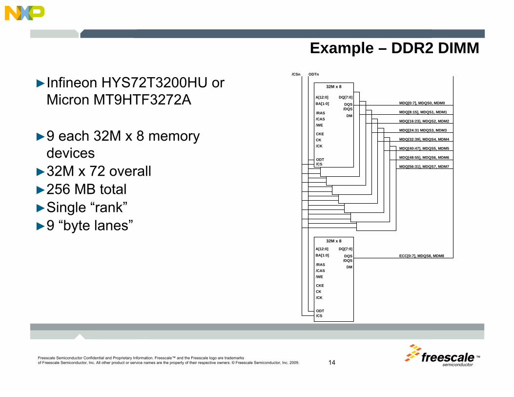
Example – DDR2 DIMM
►Infineon HYS72T3200HU or Micron MT9HTF3272A
►9 each 32M x 8 memory devices
►32M x 72 overall►256 MB total►Single “rank”►9 “byte lanes”
32M x 8
/CS
/RAS/CAS/WE
CKECK/CK
A[12:0]BA[1:0]
DQ[7:0]
DQS /DQS
DM
ODT
32M x 8
/CS
/RAS/CAS/WE
CKECK/CK
A[12:0]BA[1:0]
DQ[7:0]
DQS /DQS
ODT
MDQ[0:7], MDQS0, MDM0
MDQ[48:55], MDQS6, MDM6
MDQ[8:15], MDQS1, MDM1
MDQ[16:23], MDQS2, MDM2
MDQ[24:31 MDQS3, MDM3
MDQ[32:39], MDQS4, MDM4
MDQ[40:47], MDQS5, MDM5
MDQ[56:31], MDQS7, MDM7
ECC[0:7], MDQS8, MDM8
/CSn ODTn
DM
TMFreescale Semiconductor Confidential and Proprietary Information. Freescale™ and the Freescale logo are trademarksof Freescale Semiconductor, Inc. All other product or service names are the property of their respective owners. © Freescale Semiconductor, Inc. 2009. 15
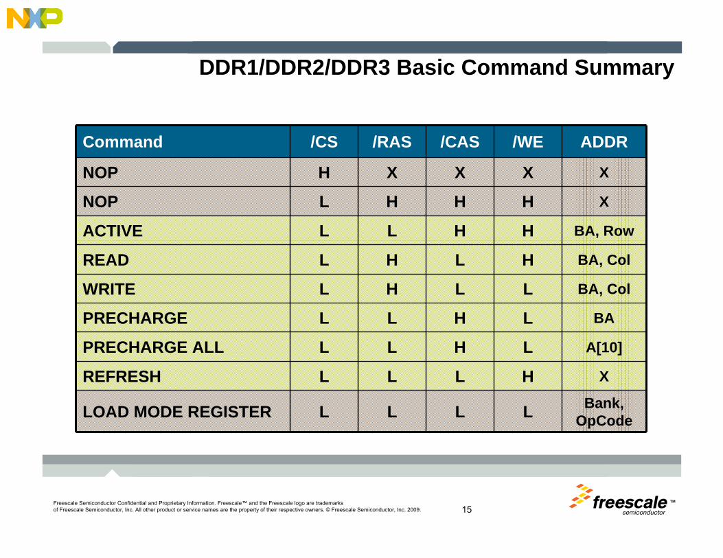
DDR1/DDR2/DDR3 Basic Command Summary
Command /CS /RAS /CAS /WE ADDR
NOP H X X X X
NOP L H H H X
ACTIVE L L H H BA, Row
READ L H L H BA, Col
WRITE L H L L BA, Col
PRECHARGE L L H L BA
PRECHARGE ALL L L H L A[10]
REFRESH L L L H X
LOAD MODE REGISTER L L L L Bank, OpCode

TMFreescale Semiconductor Confidential and Proprietary Information. Freescale™ and the Freescale logo are trademarksof Freescale Semiconductor, Inc. All other product or service names are the property of their respective owners. © Freescale Semiconductor, Inc. 2009. 16
DDR2-533 Read Timing Example
Trcd (ACTTORW ) = 4 clk
Tck = 3.75 ns
Tccd = 2 clk Trtp (RD_TO_PRE) = 2 clk
BA, ROW BA, COL BA, COL BA
ACTIVE READ READ PRECHARGE
CASLAT = 4 clk
D0 D1 D2 D3 D0 D1 D2 D3
Trp (PRETOACT) = 4 clk
Mem Clk
/CS
/RAS
/CAS
/WE
Address
DQS
DQ

TMFreescale Semiconductor Confidential and Proprietary Information. Freescale™ and the Freescale logo are trademarksof Freescale Semiconductor, Inc. All other product or service names are the property of their respective owners. © Freescale Semiconductor, Inc. 2009. 17
DDR2-533 Write Timing Example
Trcd (ACTTORW ) = 4 clk
Tck = 3.75 ns
BA, ROW BA, COL
ACTIVE WRITE
WR_LAT = CASL + AL -1 = 3 clk
D0 D1 D2 D3
0 0 0 0
Twr (WRREC) = 4 clk
BA
PRECHARGE
Mem Clk
/CS
/RAS
/CAS
/WE
Address
DQS
DQ
DM

TMFreescale Semiconductor Confidential and Proprietary Information. Freescale™ and the Freescale logo are trademarksof Freescale Semiconductor, Inc. All other product or service names are the property of their respective owners. © Freescale Semiconductor, Inc. 2009. 18
DDR1/DDR2/DDR3 ComparisonFeature DDR1 DDR2 DDR3
Package TSOP BGA only BGA only
Voltages 2.5V Core, 2.5V I/O 1.8V Core, 1.8V I/O 1.5V Core, 1.5V I/O
Densities 64Mb-1Gb 256Mb-4Gb 256Mb-8Gb
Internal Banks 4 4 or 8 8
Prefetch (min WRITE burst) 2 4 8
Data Rate 266-400 Mbps 400–800 Mbps 800–1600 Mbps
CAS / READ Latency 2, 2.5, 3 Clk 3, 4, 5 + AL Clk 5, 6, 7+ AL Clk
WRITE Latency 1 READ Latency - 1 CAS write Latancy
I/O Signaling SSTL_2 SSTL_18 SSTL_15
Termination Parallel termination to VTT for all signals
On-die for data group.VTT termination for
address, command, and control
On-die termination for data, address,
command, and control
Data Strobes Single Ended Single or Differential Differential

TMFreescale™ and the Freescale logo are trademarks of Freescale Semiconductor, Inc. All other product or service names are the property of their respective owners. © Freescale Semiconductor, Inc. 2009. 19
PowerQUICC DDR ControllersFeatures & Capabilities

TMFreescale Semiconductor Confidential and Proprietary Information. Freescale™ and the Freescale logo are trademarksof Freescale Semiconductor, Inc. All other product or service names are the property of their respective owners. © Freescale Semiconductor, Inc. 2009. 20
DDR1/DDR2/DDR3 Controller Features & Capabilities
►Supports most JEDEC standard x8, x16, x32 DDR1 & 2 & 3 devices►Memory device densities from 64Mb – through 4Gb►Data rates up to: 333 Mb/s for DDR1, 800 Mb/s for DDR2 and DDR3 ►Devices with 12-16 row address bits, 8-11 column address bits, 2-3
logical bank address bits►Data mask signals for sub-doubleword writes►Up to four physical banks (chip selects)►Physical bank sizes up to 4GB, total memory up to 16GB per
controller►Physical bank interleaving between 2 or 4 chip selects►Memory controller interleaving when more than 2 controllers are
available►Unbuffered or registered DIMMs

TMFreescale Semiconductor Confidential and Proprietary Information. Freescale™ and the Freescale logo are trademarksof Freescale Semiconductor, Inc. All other product or service names are the property of their respective owners. © Freescale Semiconductor, Inc. 2009. 21
DDR1/DDR2/DDR3 Controller Features & Capabilities (cont.)
►Up to 32 open pages• Open row table• Amount of time rows stay open is programmable
►Auto-precharge, globally or by chip select►Self-refresh►Up to 8 posted refreshes►Automatic or software controlled memory device initialization►ECC: 1-bit error correction, 2-bit error detection, detection of all
errors within a nibble►ECC error injection►Read-modify-write for sub-doubleword writes when using ECC►Automatic data initialization for ECC►Dynamic power management

TMFreescale Semiconductor Confidential and Proprietary Information. Freescale™ and the Freescale logo are trademarksof Freescale Semiconductor, Inc. All other product or service names are the property of their respective owners. © Freescale Semiconductor, Inc. 2009. 22
DDR2/DDR3 Controller additional Features & Capabilities
►Partial array self refresh►Address & command parity for Registered DIMM►Independent driver impedance setting for data, address/command,
and clock►Mirrored DIMM supported►Automatic CPO (operational)►Write-leveling for DDR3►Automatic ZQ calibration for DDR3►Fixed or On-the-fly Burst chop mode for DDR3►Asynchronous RESET for DDR3
TMFreescale Semiconductor Confidential and Proprietary Information. Freescale™ and the Freescale logo are trademarksof Freescale Semiconductor, Inc. All other product or service names are the property of their respective owners. © Freescale Semiconductor, Inc. 2009. 23
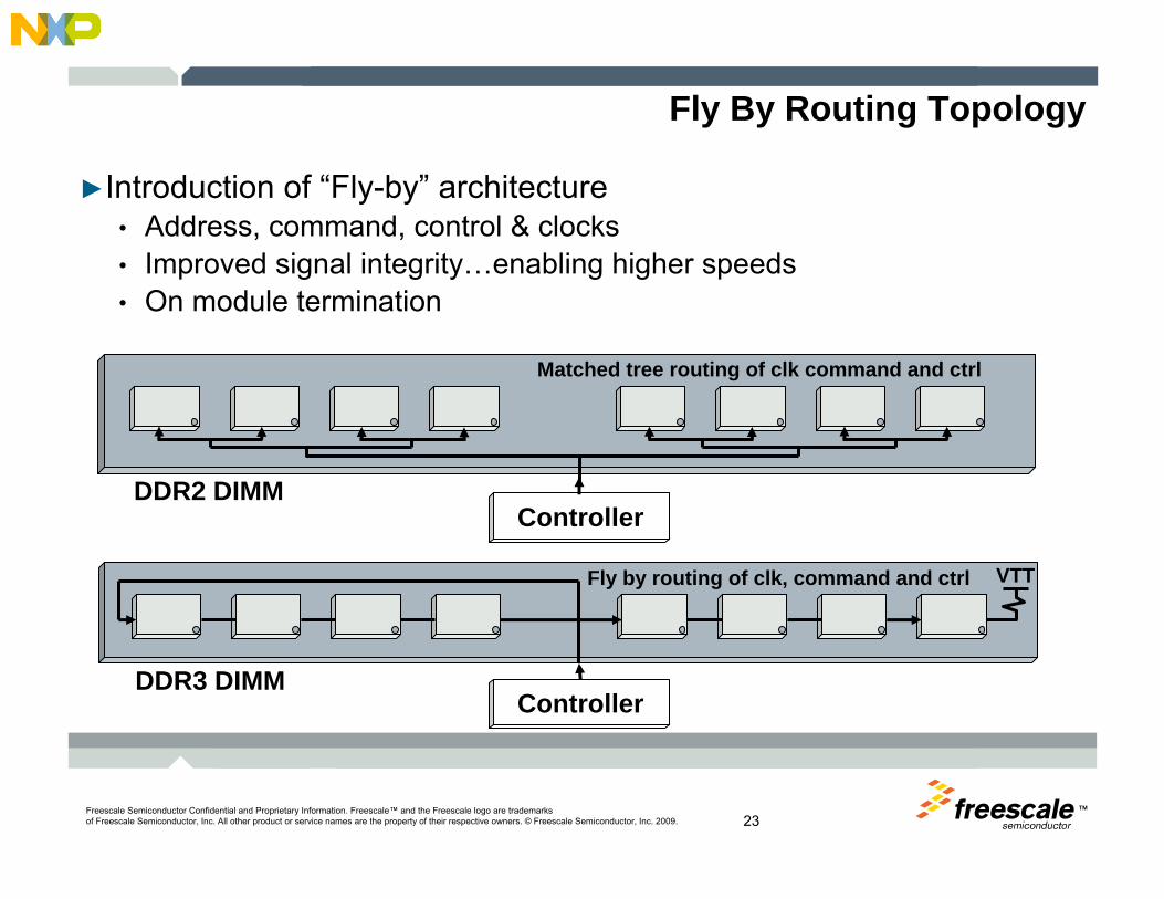
Fly By Routing Topology
►Introduction of “Fly-by” architecture • Address, command, control & clocks• Improved signal integrity…enabling higher speeds• On module termination
Controller
VTTFly by routing of clk, command and ctrl
Controller
Matched tree routing of clk command and ctrl
DDR2 DIMM
DDR3 DIMM

TMFreescale Semiconductor Confidential and Proprietary Information. Freescale™ and the Freescale logo are trademarksof Freescale Semiconductor, Inc. All other product or service names are the property of their respective owners. © Freescale Semiconductor, Inc. 2009. 24
Fly By Routing Improved SI
DDR3 Fly by routingDDR2 Matched tree routing

TMFreescale Semiconductor Confidential and Proprietary Information. Freescale™ and the Freescale logo are trademarksof Freescale Semiconductor, Inc. All other product or service names are the property of their respective owners. © Freescale Semiconductor, Inc. 2009. 25
What is write leveling
During a write cycle, the skew between the clock and strobes areincreased with the fly-by topology. The write leveling will delay the strobe (and the corresponding data lane) for each byte lane to reduce/compensate for this delay.

TMFreescale Semiconductor Confidential and Proprietary Information. Freescale™ and the Freescale logo are trademarksof Freescale Semiconductor, Inc. All other product or service names are the property of their respective owners. © Freescale Semiconductor, Inc. 2009. 26
Read Adjustment
FreescaleChip
Address, Command & Clock Bus
Data Lanes
Instead of JEDEC’s MPR method, Freescale controllers use a proprietary method of read adjust method. Auto CPO will provide the expected arrival time of preamble for each strobe line of each byte lane during the read cycle to adjust for the delays cased by the fly-by topology.
• Automatic CAS to preamble calibration
• Data strobe to data skew adjustment

TMFreescale Semiconductor Confidential and Proprietary Information. Freescale™ and the Freescale logo are trademarksof Freescale Semiconductor, Inc. All other product or service names are the property of their respective owners. © Freescale Semiconductor, Inc. 2009. 27
Write Adjustment
FreescaleChip
Address, Command & Clock Bus
Data Lanes
Write leveling sequence during the initialization process will determine the appropriate delays to each strobe/data byte lane and add this delay for every write cycle.
• Write leveling used to add delay to each strobe/data line.

TMFreescale™ and the Freescale logo are trademarks of Freescale Semiconductor, Inc. All other product or service names are the property of their respective owners. © Freescale Semiconductor, Inc. 2009. 28
PowerQUICC DDR ControllersInitialization and Register Configurations
TMFreescale Semiconductor Confidential and Proprietary Information. Freescale™ and the Freescale logo are trademarksof Freescale Semiconductor, Inc. All other product or service names are the property of their respective owners. © Freescale Semiconductor, Inc. 2009. 29
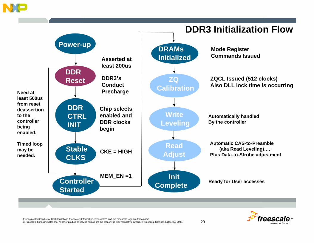
DDR3 Initialization Flow Power-up
DDRReset
DDR CTRLINIT
Chip selects enabled and DDR clocks begin
Asserted atleast 200us
StableCLKS
CKE = HIGH
DRAMsInitialized
Mode Register Commands Issued
ZQCalibration
Write Leveling
ReadAdjust
ControllerStarted
MEM_EN =1
Automatic CAS-to-Preamble (aka Read Leveling)….
Plus Data-to-Strobe adjustment
ZQCL Issued (512 clocks)Also DLL lock time is occurring
InitComplete Ready for User accesses
Automatically handledBy the controller
DDR3’s ConductPrechargeNeed at
least 500us from reset deassertion to the controller being enabled.
Timed loop may be needed.

TMFreescale Semiconductor Confidential and Proprietary Information. Freescale™ and the Freescale logo are trademarksof Freescale Semiconductor, Inc. All other product or service names are the property of their respective owners. © Freescale Semiconductor, Inc. 2009. 30
DDR2 Initialization Flow Power-up
DDR CTRLINIT
Chip selects enabled and DDR clocks begin
StableCLKS
CKE = HIGH
DRAMsInitialized
Mode Registers ProgrammedIssued by controller
DQS Adjust
ReadCalibration
ReadAdjust
ControllerStarted
MEM_EN =1
InitComplete Ready for User accesses
PrechargeAll
Issued by controller
200 us
DQS Adjust
Wait tDLL tDLL = 512 clocks

TMFreescale Semiconductor Confidential and Proprietary Information. Freescale™ and the Freescale logo are trademarksof Freescale Semiconductor, Inc. All other product or service names are the property of their respective owners. © Freescale Semiconductor, Inc. 2009. 31
Register configuration
►Two general type of registers to be configured in the memory controller
►First register type are set to the DRAM related parameter values, that are provided via SPD or DRAM datasheet
►Second register type are the Non-SPD values that are set based on customer’s application. For example:
• On-die-termination (ODT) settings for DRAM and controller• Driver impedance setting for DRAM and controller• Clock adjust, write data delay, Cast to Preamble Override (CPO)• 2T or 3T timing • Burst type selection (fixed or on-fly burst chop mode)• Write-leveling start value (WRLVL_START)
TMFreescale Semiconductor Confidential and Proprietary Information. Freescale™ and the Freescale logo are trademarksof Freescale Semiconductor, Inc. All other product or service names are the property of their respective owners. © Freescale Semiconductor, Inc. 2009. 32
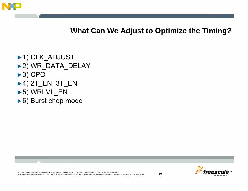
What Can We Adjust to Optimize the Timing?
►1) CLK_ADJUST►2) WR_DATA_DELAY►3) CPO►4) 2T_EN, 3T_EN►5) WRLVL_EN►6) Burst chop mode

TMFreescale Semiconductor Confidential and Proprietary Information. Freescale™ and the Freescale logo are trademarksof Freescale Semiconductor, Inc. All other product or service names are the property of their respective owners. © Freescale Semiconductor, Inc. 2009. 33
CLK_ADJUST & WR_DATA_DELAY
CLK_ADJUST = 1/2
WR_LAT = (CASL + AL -1 ) = 3
WR_DATA_DELAY = 1/2
WRITE
Internal Clock
MemClk (CLK_ADJUST = 0)
MemClk (CLK_ADJUST = 1/2)
Cmd/Addr Bus
DQS (WR_DATA_DELAY = 0)
DQ (WR_DATA_DELAY = 0)
DQS (WR_DATA_DELAY = 1/2)
DQ (WR_DATA_DELAY = 1/2)
Tdqss = ± 1/4 cycle

TMFreescale Semiconductor Confidential and Proprietary Information. Freescale™ and the Freescale logo are trademarksof Freescale Semiconductor, Inc. All other product or service names are the property of their respective owners. © Freescale Semiconductor, Inc. 2009. 34
Pitfalls / Debug Tips - Clock Adjust
►Addr/Cmd are always launched from the same location, memory clock is shifted with DDR_SDRAM_CLK_CNTL[CLK_ADJUST]
• Used to meet setup/hold for Addr/Cmd
►Use a scope to verify that clock is centered inside of the Addr/Cmd valid eye.
• Look at heavily loaded signal (/RAS, /CAS, /WE, Addr, BA)• Look at lightly loaded signal (/CS, ODT, CKE)

TMFreescale Semiconductor Confidential and Proprietary Information. Freescale™ and the Freescale logo are trademarksof Freescale Semiconductor, Inc. All other product or service names are the property of their respective owners. © Freescale Semiconductor, Inc. 2009. 35
Eye Diagrams

TMFreescale Semiconductor Confidential and Proprietary Information. Freescale™ and the Freescale logo are trademarksof Freescale Semiconductor, Inc. All other product or service names are the property of their respective owners. © Freescale Semiconductor, Inc. 2009. 36
Eye Diagrams

TMFreescale Semiconductor Confidential and Proprietary Information. Freescale™ and the Freescale logo are trademarksof Freescale Semiconductor, Inc. All other product or service names are the property of their respective owners. © Freescale Semiconductor, Inc. 2009. 37
Eye Diagrams

TMFreescale Semiconductor Confidential and Proprietary Information. Freescale™ and the Freescale logo are trademarksof Freescale Semiconductor, Inc. All other product or service names are the property of their respective owners. © Freescale Semiconductor, Inc. 2009. 38
Eye Diagrams

TMFreescale Semiconductor Confidential and Proprietary Information. Freescale™ and the Freescale logo are trademarksof Freescale Semiconductor, Inc. All other product or service names are the property of their respective owners. © Freescale Semiconductor, Inc. 2009. 39
Eye Diagrams
TMFreescale Semiconductor Confidential and Proprietary Information. Freescale™ and the Freescale logo are trademarksof Freescale Semiconductor, Inc. All other product or service names are the property of their respective owners. © Freescale Semiconductor, Inc. 2009. 40
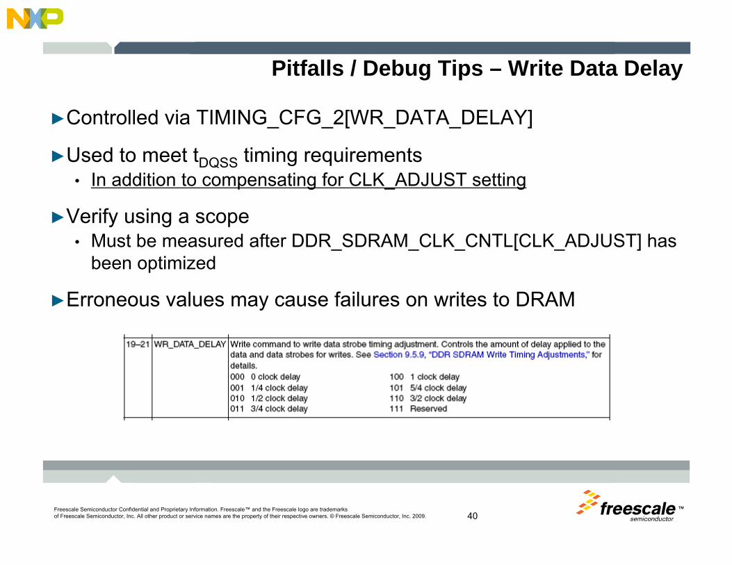
Pitfalls / Debug Tips – Write Data Delay
►Controlled via TIMING_CFG_2[WR_DATA_DELAY]
►Used to meet tDQSS timing requirements• In addition to compensating for CLK_ADJUST setting
►Verify using a scope• Must be measured after DDR_SDRAM_CLK_CNTL[CLK_ADJUST] has
been optimized
►Erroneous values may cause failures on writes to DRAM
TMFreescale Semiconductor Confidential and Proprietary Information. Freescale™ and the Freescale logo are trademarksof Freescale Semiconductor, Inc. All other product or service names are the property of their respective owners. © Freescale Semiconductor, Inc. 2009. 41
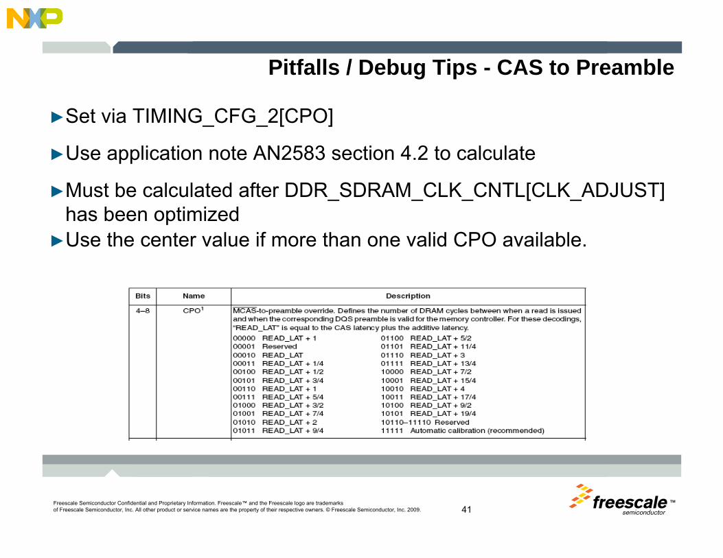
Pitfalls / Debug Tips - CAS to Preamble
►Set via TIMING_CFG_2[CPO]
►Use application note AN2583 section 4.2 to calculate
►Must be calculated after DDR_SDRAM_CLK_CNTL[CLK_ADJUST] has been optimized
►Use the center value if more than one valid CPO available.

TMFreescale Semiconductor Confidential and Proprietary Information. Freescale™ and the Freescale logo are trademarksof Freescale Semiconductor, Inc. All other product or service names are the property of their respective owners. © Freescale Semiconductor, Inc. 2009. 42
2T/3T Timing
►Puts Addr/Cmd signals on the bus for 2 or 3 clock cycles instead of 1►Does not affect Control signals
►When to use?• Two dual-rank unbuffered DIMMs• 36 loads on Addr/Cmd lines
►Typically not required for:• One dual-rank unbuffered DIMM• 18 loads on Addr/Cmd lines
►When not to use?• Registered DIMMs

TMFreescale™ and the Freescale logo are trademarks of Freescale Semiconductor, Inc. All other product or service names are the property of their respective owners. © Freescale Semiconductor, Inc. 2009. 43
PowerQUICC DDR ControllersPitfalls / Debug Tips

TMFreescale Semiconductor Confidential and Proprietary Information. Freescale™ and the Freescale logo are trademarksof Freescale Semiconductor, Inc. All other product or service names are the property of their respective owners. © Freescale Semiconductor, Inc. 2009. 44
Pitfalls / Debug Tips - DDR Type POR Configuration
TMFreescale Semiconductor Confidential and Proprietary Information. Freescale™ and the Freescale logo are trademarksof Freescale Semiconductor, Inc. All other product or service names are the property of their respective owners. © Freescale Semiconductor, Inc. 2009. 45
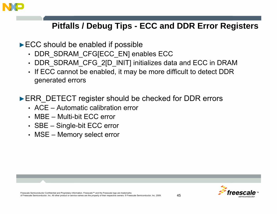
Pitfalls / Debug Tips - ECC and DDR Error Registers
►ECC should be enabled if possible• DDR_SDRAM_CFG[ECC_EN] enables ECC• DDR_SDRAM_CFG_2[D_INIT] initializes data and ECC in DRAM• If ECC cannot be enabled, it may be more difficult to detect DDR
generated errors
►ERR_DETECT register should be checked for DDR errors• ACE – Automatic calibration error• MBE – Multi-bit ECC error• SBE – Single-bit ECC error• MSE – Memory select error

TMFreescale Semiconductor Confidential and Proprietary Information. Freescale™ and the Freescale logo are trademarksof Freescale Semiconductor, Inc. All other product or service names are the property of their respective owners. © Freescale Semiconductor, Inc. 2009. 46
Pitfalls / Debug Tips - CAS Latency / Write Latency / Additive Latency
►Program write latency based on DRAM type• DDR1 -> Write latency = 1 DRAM cycle• DDR2 -> Write latency = (Read latency – 1) DRAM cycles• DDR3 -> Write latency = CWL
►Programming CAS latency too high can degrade performance• Check DRAM datasheet based on frequency used and specific DRAM
device
►When ODT is used, other rules must be followed to allow ODT to assert early enough
• DDR2: Write latency + additive latency >= 3 cycles• DDR3: TIMING_CFG_5 [WODT_ON], [WODT_OFF] = WL-1 cycles for
fixed or fly-by burst chop

TMFreescale Semiconductor Confidential and Proprietary Information. Freescale™ and the Freescale logo are trademarksof Freescale Semiconductor, Inc. All other product or service names are the property of their respective owners. © Freescale Semiconductor, Inc. 2009. 47
Pitfalls / Debug Tips - DDR Mode Registers
►Values programmed into DDR mode registers must match DDR controller configuration registers
• CAS latency• Burst length• Write recovery
Not a straight decode in Mode Register• Active powerdown exit time• Additive latency• Differential DQS enable
►DLL reset and OCD calibration fields are controlled automatically by the DDR controller

TMFreescale Semiconductor Confidential and Proprietary Information. Freescale™ and the Freescale logo are trademarksof Freescale Semiconductor, Inc. All other product or service names are the property of their respective owners. © Freescale Semiconductor, Inc. 2009. 48
*Pitfalls / Debug Tips - Programming twtr, trrd, and trtp
►Use caution when calculating:
• TIMING_CFG_1[WRTORD] (twtr)
• TIMING_CFG_1[ACTTOACT] (trrd)
• TIMING_CFG_2[RD_TO_PRE] (trtp)
• DDR2: Minimum value for each parameter is 2 DRAM clocks• DDR3: Minimum value for each parameter is 4 DRAM clocks

TMFreescale Semiconductor Confidential and Proprietary Information. Freescale™ and the Freescale logo are trademarksof Freescale Semiconductor, Inc. All other product or service names are the property of their respective owners. © Freescale Semiconductor, Inc. 2009. 49
Pitfalls / Debug Tips - 200 us Delay
►200 μs for DDR2 and 512 us for DDR3 must pass between stable clocks and CKE assertion
►Clocks are stable after DDR_SDRAM_CLK_CNTL[CLK_ADJUST] is programmed and any chip select has been enabled via CSn_CONFIG[CS_n_EN]
►CKE is asserted after DDR_SDRAM_CFG[MEM_EN] is set
►Software must provide delay between these 2 steps

TMFreescale™ and the Freescale logo are trademarks of Freescale Semiconductor, Inc. All other product or service names are the property of their respective owners. © Freescale Semiconductor, Inc. 2009. 50
References
TMFreescale Semiconductor Confidential and Proprietary Information. Freescale™ and the Freescale logo are trademarksof Freescale Semiconductor, Inc. All other product or service names are the property of their respective owners. © Freescale Semiconductor, Inc. 2009. 51
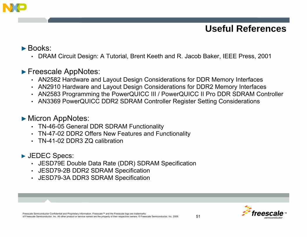
Useful References
►Books:• DRAM Circuit Design: A Tutorial, Brent Keeth and R. Jacob Baker, IEEE Press, 2001
►Freescale AppNotes:• AN2582 Hardware and Layout Design Considerations for DDR Memory Interfaces• AN2910 Hardware and Layout Design Considerations for DDR2 Memory Interfaces• AN2583 Programming the PowerQUICC III / PowerQUICC II Pro DDR SDRAM Controller• AN3369 PowerQUICC DDR2 SDRAM Controller Register Setting Considerations
►Micron AppNotes:• TN-46-05 General DDR SDRAM Functionality• TN-47-02 DDR2 Offers New Features and Functionality• TN-41-02 DDR3 ZQ calibration
► JEDEC Specs:• JESD79E Double Data Rate (DDR) SDRAM Specification• JESD79-2B DDR2 SDRAM Specification• JESD79-3A DDR3 SDRAM Specification

TMFreescale™ and the Freescale logo are trademarks of Freescale Semiconductor, Inc. All other product or service names are the property of their respective owners. © Freescale Semiconductor, Inc. 2009. 52
Q&A
►Thank you for attending this presentation. We’ll now take a few moments for the audience’s questions and then we’ll begin the question and answer session.

TM