enpirion power datasheet efficiency vs. output current ... · pdf fileenpirion® power...
TRANSCRIPT
Enpirion® Power Datasheet EV1320QI 2A PowerSoC
Source/Sink DDR Memory Termination Converter
www.altera.com/enpirion
Description
The EV1320QI is a DC to DC converter specifically designed for memory termination applications. The device offers high efficiency, up to 96%, while providing a solution footprint similar to that of a linear termination device.
The EV1320QI comes in a 3mm x 3mm x 0.55mm QFN 16-pin package and requires only a small number of external MLCC capacitors. The device is designed to operate directly from the VDDQ supply rail. No external divider or reference is required. The EV1320QI provides a very stable output voltage (VTT) which tracks VDDQ while sinking and sourcing up to 2A of continuous output current. Up to 4 EV1320QI devices can be paralleled to source up to 8A of current. An ENABLE pin with output discharge is available for S3 (suspend to RAM) states. EV1320QI is specifically designed to meet the precise voltage, fast transient requirements of present and future high-performance, DDR2, DDR3, DDR4, QDR, and low power DDR3/DDR4 JEDEC VTT requirements. Advanced circuit techniques and high switching frequency deliver high-quality, compact, non-isolated DC-DC conversion.
Features
High Efficiency, Up to 96%
40mm2 Total Solution Size
No External Inductor Required
JEDEC Compliant DDR2/3/4/QDR and Low Power DDR3/4 Solution
Enable Pin with Output Discharge to Support S3 (Suspend to RAM) Mode
Operates Directly from VDDQ
VOUT (VTT) Voltage Tracks VDDQ/2 ± 40mV
Source and Sink Up to 2A Continuous Current
Parallel Up to 4 Devices for 8A VTT Current
Programmable Soft Start/Soft Shutdown
Cost Effective Integrated Solution
Thermal Overload, Over Current, Short Circuit, and Under-Voltage Protection
RoHS Compliant, MSL level 3, 260C Reflow
Applications
VTT Bus Termination for DDR2, DDR3, DDR4, Low Power DDR3, DDR4, and QDR Memories
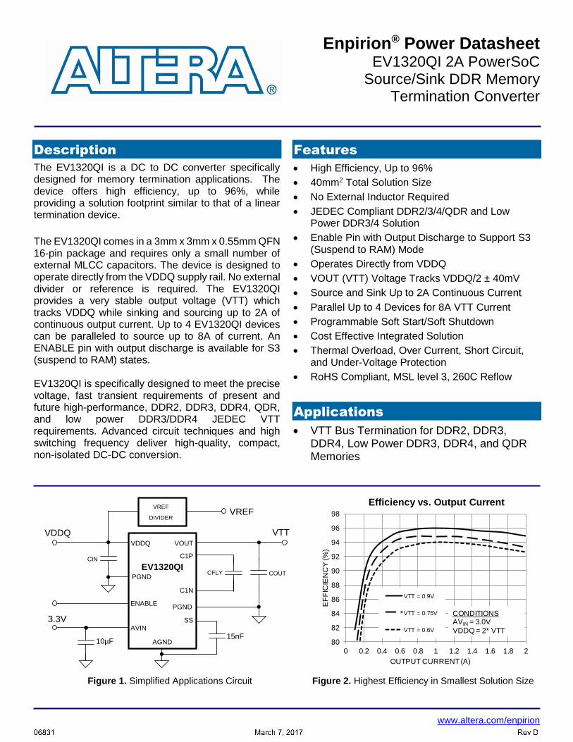
VTT
C1P
COUT
CIN
VOUT
AVIN
AGND
SS
VDDQ
ENABLE
PGND
PGND
C1N
15nF
CFLY
VDDQ
3.3V
VREF
DIVIDERVREF
EV1320QI
10µF
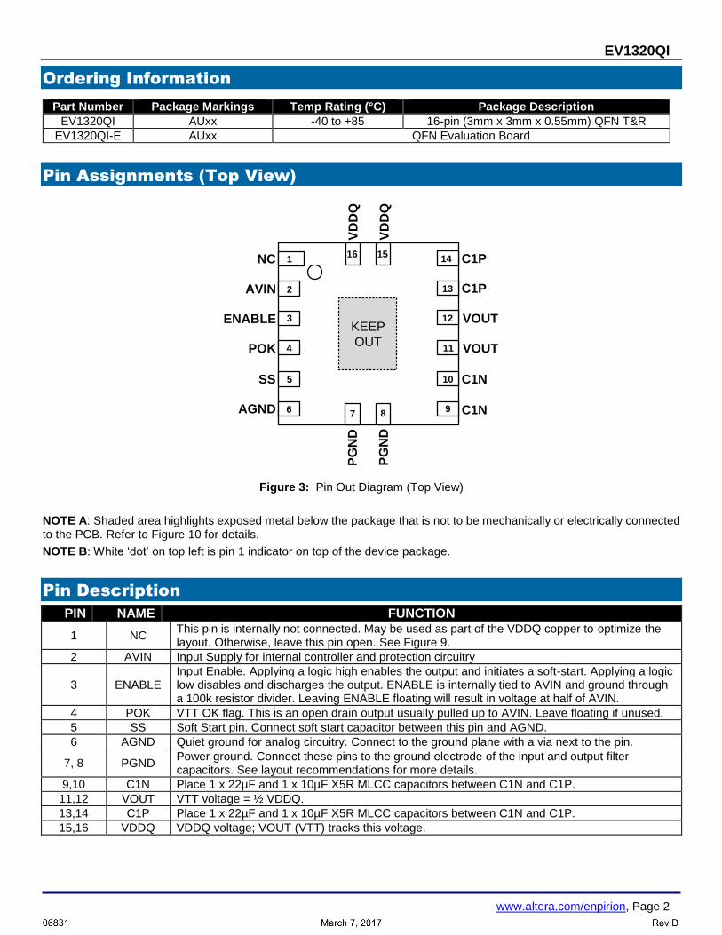
Figure 1. Simplified Applications Circuit Figure 2. Highest Efficiency in Smallest Solution Size
80
82
84
86
88
90
92
94
96
98
0 0.2 0.4 0.6 0.8 1 1.2 1.4 1.6 1.8 2
EF
FIC
IEN
CY
(%
)
OUTPUT CURRENT (A)
Efficiency vs. Output Current
VTT = 0.9V
VTT = 0.75V
VTT = 0.6V
CONDITIONSAVIN = 3.0V
VDDQ = 2* VTT
EV1320QI
www.altera.com/enpirion, Page 2
Ordering Information
Part Number Package Markings Temp Rating (°C) Package Description
EV1320QI AUxx -40 to +85 16-pin (3mm x 3mm x 0.55mm) QFN T&R
EV1320QI-E AUxx QFN Evaluation Board
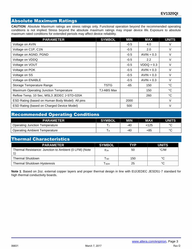
Pin Assignments (Top View)
NC 1
AVIN
ENABLE
POK
SS
AGND
PG
ND
PG
ND
C1N
C1N
VOUT
VOUT
C1P
C1P
VD
DQ
VD
DQ
2
3
4
5
6 7 89
10
11
12
13
141516
KEEP
OUT
Figure 3: Pin Out Diagram (Top View)
NOTE A: Shaded area highlights exposed metal below the package that is not to be mechanically or electrically connected to the PCB. Refer to Figure 10 for details.
NOTE B: White ‘dot’ on top left is pin 1 indicator on top of the device package.
Pin Description
PIN NAME FUNCTION
1 NC This pin is internally not connected. May be used as part of the VDDQ copper to optimize the layout. Otherwise, leave this pin open. See Figure 9.
2 AVIN Input Supply for internal controller and protection circuitry
3 ENABLE Input Enable. Applying a logic high enables the output and initiates a soft-start. Applying a logic low disables and discharges the output. ENABLE is internally tied to AVIN and ground through a 100k resistor divider. Leaving ENABLE floating will result in voltage at half of AVIN.
4 POK VTT OK flag. This is an open drain output usually pulled up to AVIN. Leave floating if unused.
5 SS Soft Start pin. Connect soft start capacitor between this pin and AGND.
6 AGND Quiet ground for analog circuitry. Connect to the ground plane with a via next to the pin.
7, 8 PGND Power ground. Connect these pins to the ground electrode of the input and output filter capacitors. See layout recommendations for more details.
9,10 C1N Place 1 x 22µF and 1 x 10µF X5R MLCC capacitors between C1N and C1P.
11,12 VOUT VTT voltage = ½ VDDQ.
13,14 C1P Place 1 x 22µF and 1 x 10µF X5R MLCC capacitors between C1N and C1P.
15,16 VDDQ VDDQ voltage; VOUT (VTT) tracks this voltage.
EV1320QI
www.altera.com/enpirion, Page 3
Absolute Maximum Ratings
CAUTION: Absolute Maximum ratings are stress ratings only. Functional operation beyond the recommended operating conditions is not implied. Stress beyond the absolute maximum ratings may impair device life. Exposure to absolute maximum rated conditions for extended periods may affect device reliability.
PARAMETER SYMBOL MIN MAX UNITS
Voltage on AVIN -0.5 4.0 V
Voltage on C1P, C1N -0.5 2.0 V
Voltage on AGND, PGND -0.5 AVIN + 0.3 V
Voltage on VDDQ -0.5 2.2 V
Voltage on VOUT -0.5 VDDQ + 0.3 V
Voltage on POK -0.5 AVIN + 0.3 V
Voltage on SS -0.5 AVIN + 0.3 V
Voltage on ENABLE -0.5 AVIN + 0.3 V
Storage Temperature Range TSTG -65 150 °C
Maximum Operating Junction Temperature TJ-ABS Max 150 °C
Reflow Temp, 10 Sec, MSL3 JEDEC J-STD-020A 260 °C
ESD Rating (based on Human Body Model): All pins 2000 V
ESD Rating (based on Charged Device Model) 500 V
Recommended Operating Conditions
PARAMETER SYMBOL MIN MAX UNITS
Operating Junction Temperature TJ -40 +125 °C
Operating Ambient Temperature TA -40 +85 °C
Thermal Characteristics
PARAMETER SYMBOL TYP UNITS
Thermal Resistance: Junction to Ambient (0 LFM) (Note 1)
JA 50 °C/W
Thermal Shutdown TSD 150 °C
Thermal Shutdown Hysteresis TSDH 25 °C
Note 1: Based on 2oz. external copper layers and proper thermal design in line with EIJ/JEDEC JESD51-7 standard for high thermal conductivity boards.
EV1320QI
www.altera.com/enpirion, Page 4
Electrical Characteristics
NOTE: AVIN = 3.3V; VDDQ = 1.5V. Minimum and Maximum values are over operating ambient temperature range unless otherwise noted. Typical values are at TA = 25°C.
PARAMETER SYMBOL TEST CONDITIONS MIN TYP MAX UNITS
VDDQ voltage range VDDQ 0.95 1.5 1.8 V
AVIN voltage range AVIN 3.0 3.3 3.465 V
VTT Tracking Accuracy DC
(NOTE 2) ∆VTT
AVIN=3.3V±5%
0A IVTT 2A
0.49*
VDDQ
40
0.51*
VDDQ + 40
mV
Under Voltage Lockout; AVIN rising
VUVLO 2.5 V
Under Voltage Lockout; AVIN falling
VUVLO 2.2 V
AVIN Shut-Down Supply Current
IS ENABLE=Low 600 A
VDDQ Shut-Down Supply Current
IS ENABLE=Low 200 A
AVIN No Load Operating Current
IAVIN AVIN=3.3V 6 mA
VDDQ No Load Operating Current
IVDDQ AVIN=3.3V 750 A
Switching Frequency FSW 500 625 750 kHz
POK Threshold Sourcing Current
VOUT Rising 95 %
POK Threshold Sourcing Current
VOUT Falling 85 %
POK Low Voltage ISINK = 1mA
0.15 0.4 V
POK Pin VOH Leakage Current
AVIN = 3.3V
POK High 25 A
Output Impedance ROUT VOUT/ILOAD 20 m
Continuous Output Current;
I_Max_Source VDDQ=1.5V
AVIN=3.3V -2 2 A
Over Current Trip Level
IOCP AVIN=3.3V ±4.5 A
Enable Threshold Logic Low
ENA_VIL Max voltage to ensure the converter is disabled
0.3 V
Enable Threshold Logic High
ENA_VIH 3.0V ≤ AVIN ≤ 3.46V AVIN –
0.5 AVIN V
Enable Input Current 100 200 µA
Note 2: As measured at the bulk capacitors at the edge of EV1320QI evaluation board. Complies with JEDEC DDR2 and DDR3 VDDQ tracking specification.
EV1320QI
www.altera.com/enpirion, Page 5
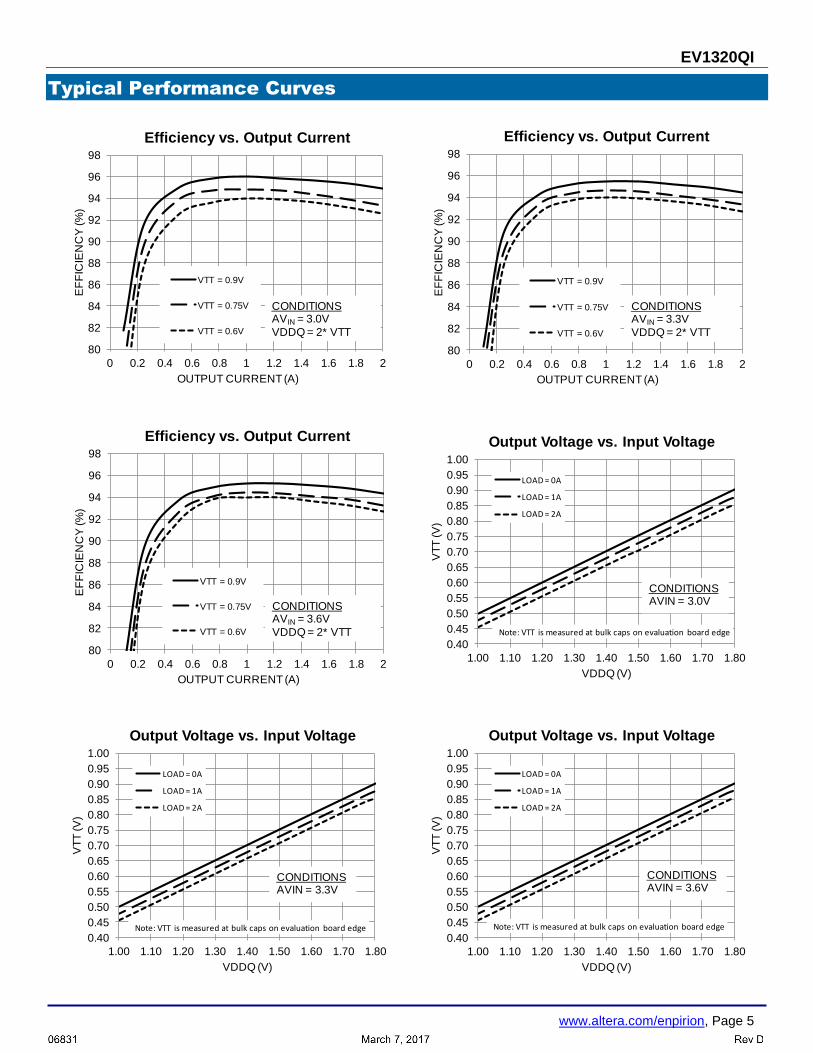
Typical Performance Curves
80
82
84
86
88
90
92
94
96
98
0 0.2 0.4 0.6 0.8 1 1.2 1.4 1.6 1.8 2
EF
FIC
IEN
CY
(%
)
OUTPUT CURRENT (A)
Efficiency vs. Output Current
VTT = 0.9V
VTT = 0.75V
VTT = 0.6V
CONDITIONSAVIN = 3.0V
VDDQ = 2* VTT
80
82
84
86
88
90
92
94
96
98
0 0.2 0.4 0.6 0.8 1 1.2 1.4 1.6 1.8 2
EF
FIC
IEN
CY
(%
)
OUTPUT CURRENT (A)
Efficiency vs. Output Current
VTT = 0.9V
VTT = 0.75V
VTT = 0.6V
CONDITIONSAVIN = 3.3V
VDDQ = 2* VTT
80
82
84
86
88
90
92
94
96
98
0 0.2 0.4 0.6 0.8 1 1.2 1.4 1.6 1.8 2
EF
FIC
IEN
CY
(%
)
OUTPUT CURRENT (A)
Efficiency vs. Output Current
VTT = 0.9V
VTT = 0.75V
VTT = 0.6V
CONDITIONSAVIN = 3.6V
VDDQ = 2* VTT0.40
0.45
0.50
0.55
0.60
0.65
0.70
0.75
0.80
0.85
0.90
0.95
1.00
1.00 1.10 1.20 1.30 1.40 1.50 1.60 1.70 1.80
VT
T (
V)
VDDQ (V)
Output Voltage vs. Input Voltage
LOAD = 0A
LOAD = 1A
LOAD = 2A
CONDITIONSAVIN = 3.0V
Note: VTT is measured at bulk caps on evaluation board edge
0.40
0.45
0.50
0.55
0.60
0.65
0.70
0.75
0.80
0.85
0.90
0.95
1.00
1.00 1.10 1.20 1.30 1.40 1.50 1.60 1.70 1.80
VT
T (
V)
VDDQ (V)
Output Voltage vs. Input Voltage
LOAD = 0A
LOAD = 1A
LOAD = 2A
CONDITIONSAVIN = 3.3V
Note: VTT is measured at bulk caps on evaluation board edge0.40
0.45
0.50
0.55
0.60
0.65
0.70
0.75
0.80
0.85
0.90
0.95
1.00
1.00 1.10 1.20 1.30 1.40 1.50 1.60 1.70 1.80
VT
T (
V)
VDDQ (V)
Output Voltage vs. Input Voltage
LOAD = 0A
LOAD = 1A
LOAD = 2A
CONDITIONSAVIN = 3.6V
Note: VTT is measured at bulk caps on evaluation board edge

EV1320QI
www.altera.com/enpirion, Page 6
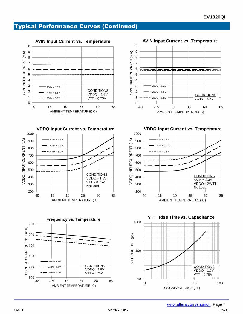
Typical Performance Curves (Continued)
0.54
0.55
0.56
0.57
0.58
0.59
0.60
0.61
0.62
0.63
0.64
0 0.2 0.4 0.6 0.8 1 1.2 1.4 1.6 1.8 2
VT
T (
V)
OUTPUT CURRENT (A)
Output Voltage vs. Output Current
TA = -45 C
TA = 25 C
TA = 85 C
CONDITIONSAVIN = 3.3V
VDDQ = 1.2VVTT = 0.6V
Note: VTT is measured at bulk caps on evaluation board edge
0.70
0.71
0.72
0.73
0.74
0.75
0.76
0.77
0.78
0.79
0.80
0 0.2 0.4 0.6 0.8 1 1.2 1.4 1.6 1.8 2
VT
T (
V)
OUTPUT CURRENT (A)
Output Voltage vs. Output Current
TA = -45 C
TA = 25 C
TA = 85 C
CONDITIONSAVIN = 3.3V
VDDQ = 1.5VVTT = 0.75V
Note: VTT is measured at bulk caps on evaluation board edge
0.84
0.85
0.86
0.87
0.88
0.89
0.90
0.91
0.92
0.93
0.94
0 0.2 0.4 0.6 0.8 1 1.2 1.4 1.6 1.8 2
VT
T (
V)
OUTPUT CURRENT (A)
Output Voltage vs. Output Current
TA = -40 C
TA = 25 C
TA = 85 C
CONDITIONSAVIN = 3.3V
VDDQ = 1.8V
CONDITIONSAVIN = 3.3V
VDDQ = 1.8VVTT = 0.9V
Note: VTT is measured at bulk caps on evaluation board edge0.50
0.52
0.54
0.56
0.58
0.60
0.62
0.64
0.66
0.68
0.70
-40 -15 10 35 60 85
VT
T (
V)
AMBIENT TEMPERATURE ( C)
Output Voltage vs. Temperature
LOAD = 0A
LOAD = 1A
LOAD = 2A
CONDITIONSAVIN=3.3V
VDDQ = 1.2V
Note: VTT is measured at bulk caps on evaluation board edge
0.65
0.67
0.69
0.71
0.73
0.75
0.77
0.79
0.81
0.83
0.85
-40 -15 10 35 60 85
VT
T (
V)
AMBIENT TEMPERATURE ( C)
Output Voltage vs. Temperature
LOAD = 0A
LOAD = 1A
LOAD = 2A
CONDITIONSAVIN=3.3V
VDDQ = 1.5V
Note: VTT is measured at bulk caps on evaluation board edge
0.80
0.82
0.84
0.86
0.88
0.90
0.92
0.94
0.96
0.98
1.00
-40 -15 10 35 60 85
VT
T (
V)
AMBIENT TEMPERATURE ( C)
Output Voltage vs. Temperature
LOAD = 0A
LOAD = 1A
LOAD = 2A
CONDITIONSAVIN=3.3V
VDDQ = 1.8V
Note: VTT is measured at bulk caps on evaluation board edge
EV1320QI
www.altera.com/enpirion, Page 7
Typical Performance Curves (Continued)
0
1
2
3
4
5
6
7
8
9
10
-40 -15 10 35 60 85
AV
IN I
NP
UT
CU
RR
EN
T (m
A)
AMBIENT TEMPERATURE( C)
AVIN Input Current vs. Temperature
AVIN = 3.6V
AVIN = 3.3V
AVIN = 3.0V
CONDITIONSVDDQ = 1.5V
VTT = 0.75V
0
1
2
3
4
5
6
7
8
9
10
-40 -15 10 35 60 85
AV
IN I
NP
UT
CU
RR
EN
T (m
A)
AMBIENT TEMPERATURE( C)
AVIN Input Current vs. Temperature
VDDQ = 1.2V
VDDQ = 1.5V
VDDQ = 1.8VCONDITIONSAVIN = 3.3V
200
300
400
500
600
700
800
900
1000
-40 -15 10 35 60 85
VD
DQ
IN
PU
T C
UR
RE
NT
(µ
A)
AMBIENT TEMPERATURE( C)
VDDQ Input Current vs. Temperature
AVIN = 3.6V
AVIN = 3.3V
AVIN = 3.0V
CONDITIONSVDDQ = 1.5V
VTT = 0.75VNo Load
200
300
400
500
600
700
800
900
1000
-40 -15 10 35 60 85
VD
DQ
IN
PU
T C
UR
RE
NT
(µ
A)
AMBIENT TEMPERATURE( C)
VDDQ Input Current vs. Temperature
VTT = 0.6V
VTT = 0.75V
VTT = 0.9V
CONDITIONSAVIN = 3.3V
VDDQ = 2*VTTNo Load
500
550
600
650
700
750
-40 -15 10 35 60 85
OS
CIL
LA
TO
R F
RE
QU
EN
CY
(kH
z)
AMBIENT TEMPERATURE( C)
Frequency vs. Temperature
AVIN = 3.6V
AVIN = 3.3V
AVIN = 3.0V
CONDITIONSVDDQ = 1.5V
VTT = 0.75V
10
100
1000
0.1 1 10 100
VT
T R
ISE
TIM
E (
µs)
SS CAPACITANCE (nF)
VTT Rise Time vs. Capacitance
CONDITIONSVDDQ = 1.5V
VTT = 0.75V
EV1320QI
www.altera.com/enpirion, Page 8
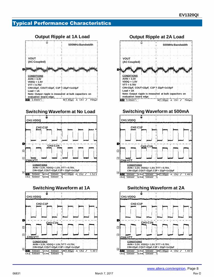
Typical Performance Characteristics
VOUT
(AC Coupled)
Output Ripple at 1A Load
CONDITIONS
AVIN = 3.3V
VDDQ = 1.5V
VTT = 0.75V
CIN=22µF, COUT=22µF, C1P = 22µF+1x10µF
Load = 1A
Note: Output ripple is measured at bulk capacitors on
evaluation board edge
500MHz Bandwidth
VOUT
(AC Coupled)
Output Ripple at 2A Load
CONDITIONS
AVIN = 3.3V
VDDQ = 1.5V
VTT = 0.75V
CIN=22µF, COUT=22µF, C1P = 22µF+1x10µF
Load = 2A
Note: Output ripple is measured at bulk capacitors on
evaluation board edge
500MHz Bandwidth
Switching Waveform at No Load
CONDITIONS
AVIN = 3.3V, VDDQ = 1.5V, VTT = 0.75V,
CIN=22µF, COUT=22µF, C1P = 22µF+1x10µF
CH1:VDDQ
CH2:C1P
CH3:C1N
CH4:VTT
Switching Waveform at 500mA
CONDITIONS
AVIN = 3.3V, VDDQ = 1.5V, VTT = 0.75V,
CIN=22µF, COUT=22µF, C1P = 22µF+1x10µF
CH1:VDDQ
CH2:C1P
CH3:C1N
CH4:VTT
Switching Waveform at 1A
CONDITIONS
AVIN = 3.3V, VDDQ = 1.5V, VTT = 0.75V,
CIN=22µF, COUT=22µF, C1P = 22µF+1x10µF
CH1:VDDQ
CH2:C1P
CH3:C1N
CH4:VTT
Switching Waveform at 2A
CONDITIONS
AVIN = 3.3V, VDDQ = 1.5V, VTT = 0.75V,
CIN=22µF, COUT=22µF, C1P = 22µF+1x10µF
CH1:VDDQ
CH2:C1P
CH3:C1N
CH4:VTT
EV1320QI
www.altera.com/enpirion, Page 9
Typical Performance Characteristics (Continued)
VTT
(AC Coupled)
Load Transient from 0 to 500mA
CONDITIONS
AVIN = 3.3V
VDDQ = 1.5V
VTT = 0.75V
CIN=22µF, COUT=22µF
C1P = 22µF+1x10µF)
LOAD
VDDQ
(AC Coupled)
ΔVTT is due to ΔVDDQ
Note: Output deviation is measured at bulk capacitors on
evaluation board edge
VTT
(AC Coupled)
Load Transient from 0 to 1A
CONDITIONS
AVIN = 3.3V
VDDQ = 1.5V
VTT = 0.75V
CIN=22µF, COUT=22µF
C1P = 22µF+1x10µF
LOAD
VDDQ
(AC Coupled)
ΔVTT is due to ΔVDDQ
Note: Output deviation is measured at bulk capacitors on
evaluation board edge
VTT
(AC Coupled)
Load Transient from 0 to 1.5A
CONDITIONS
AVIN = 3.3V
VDDQ = 1.5V
VTT = 0.75V
CIN=22µF, COUT=22µF
C1P = 22µF+1x10µFLOAD
VDDQ
(AC Coupled)
ΔVTT is due to ΔVDDQ
Note: Output deviation is measured at bulk capacitors on
evaluation board edge
VTT
(AC Coupled)
Load Transient from 0 to 2A
CONDITIONS
AVIN = 3.3V
VDDQ = 1.5V
VTT = 0.75V
CIN=22µF, COUT=22µF
C1P = 22µF+1x10µF
LOAD
VDDQ
(AC Coupled)
ΔVTT is due to ΔVDDQ
Note: Output deviation is measured at bulk capacitors on
evaluation board edge
VDDQ
(AC Coupled)
VDDQ to VTT Tracking with Line
CONDITIONS
LOAD = 1Ω
AVIN = 3.3V,
CIN=22µF, COUT=22µF, C1P = 22µF+1x10µF
VTT
(AC Coupled)
ΔVTT is due to ΔVDDQ
ENABLE
Startup with POK at No Load
VDDQ
CONDITIONS
No Load
CSS = 15nF
AVIN = 3.3V, VDDQ = 1.2V, VTT = 0.6V,
CIN=22µF, COUT=22µF, C1P = 22µF+1x10µF
VTT
POK
EV1320QI
www.altera.com/enpirion, Page 10
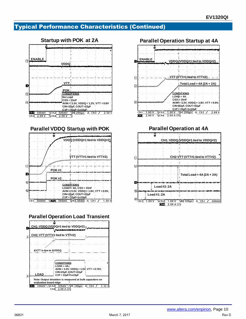
Typical Performance Characteristics (Continued)
ENABLE
Startup with POK at 2A
VDDQ
CONDITIONS
No Load
CSS = 15nF
AVIN = 3.3V, VDDQ = 1.2V, VTT = 0.6V
CIN=22µF, COUT=22µF
C1P = 22µF+1x10µF
VTT
POK
ENABLE
Parallel Operation Startup at 4A
VDDQ (VDDQ#1 tied to VDDQ#2)
CONDITIONS
LOAD = 4A
CSS = 15nF
AVIN = 3.3V, VDDQ = 1.8V, VTT = 0.9V,
CIN=22µF, COUT=22µF
C1P = 22µF+1x10µF
VTT (VTT#1 tied to VTT#2)
Total Load = 4A (2A + 2A)
Parallel VDDQ Startup with POK
VDDQ (VDDQ#1 tied to VDDQ#2)
CONDITIONS
LOAD = 4A, CSS = 15nF
AVIN = 3.3V, VDDQ = 1.8V, VTT = 0.9V,
CIN=22µF, COUT=22µF
C1P = 22µF+1x10µF
VTT (VTT#1 tied to VTT#2)
POK #1
POK #2
Parallel Operation at 4A
CH1: VDDQ (VDDQ#1 tied to VDDQ#2)
CH2:VTT (VTT#1 tied to VTT#2)
Total Load = 4A (2A + 2A)
Load #2: 2A
Load #1: 2A
Parallel Operation Load Transient
CH1: VDDQ (VDDQ#1 tied to VDDQ#2)
CONDITIONS
LOAD = 4A
AVIN = 3.3V, VDDQ = 1.5V, VTT = 0.75V,
CIN=22µF, COUT=22µF
C1P = 22µF+1x10µF
CH2: VTT (VTT#1 tied to VTT#2)
LOAD
ΔVTT is due to ΔVDDQ
Note: Output deviation is measured at bulk capacitors on
evaluation board edge
EV1320QI
www.altera.com/enpirion, Page 11
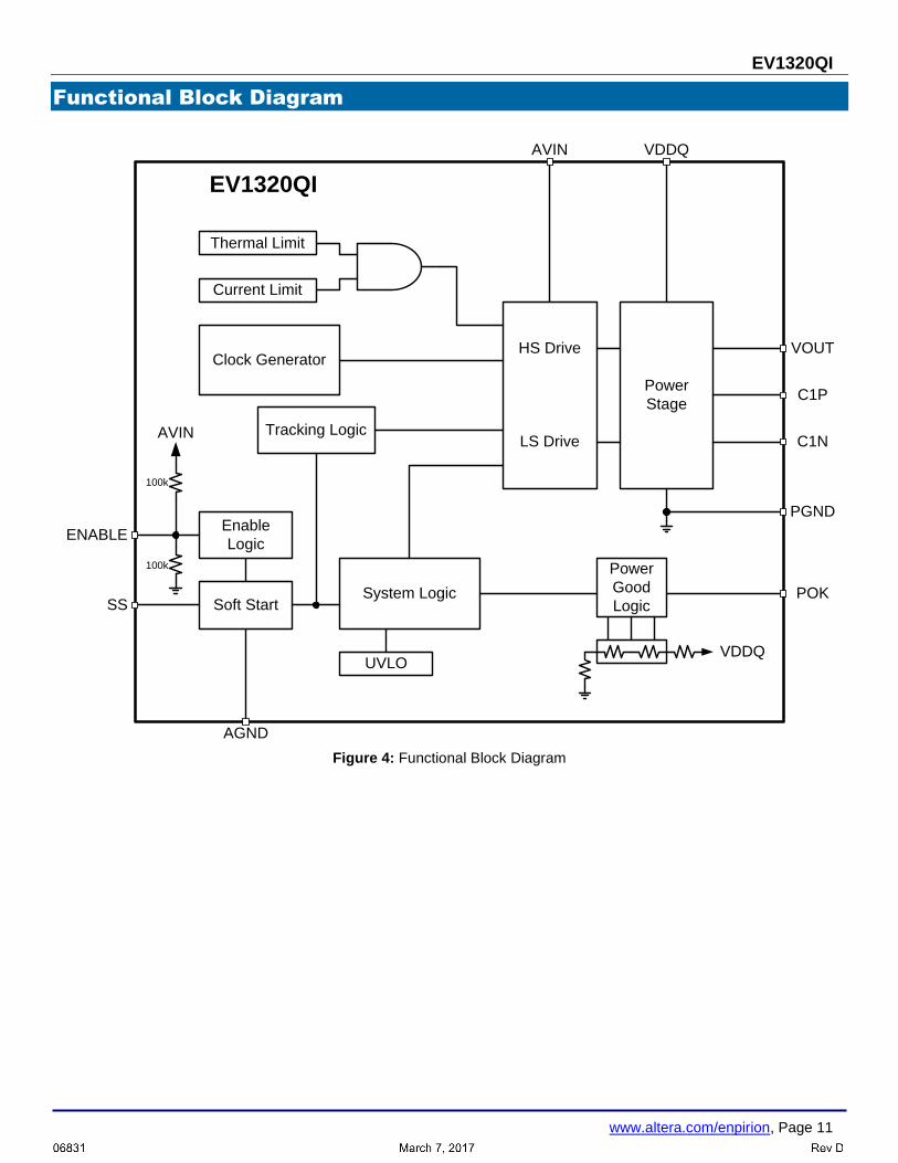
Functional Block Diagram
System LogicSoft Start
Thermal Limit
Current Limit
UVLO
Power
Good
Logic
HS Drive
LS Drive
Clock Generator
Tracking Logic
Enable
Logic
VDDQ
VDDQ
VOUT
C1P
C1N
PGND
POK
ENABLE
SS
AGND
AVIN
EV1320QI
Power
Stage
AVIN
100k
100k
Figure 4: Functional Block Diagram
EV1320QI
www.altera.com/enpirion, Page 12
Functional Description
VDDQ/VTT Converter
The EV1320QI is designed to replace low efficiency linear regulators as well as expensive switch-mode DCDC memory terminations. The patented EV1320QI architecture provides efficiencies up to 96% with a solution footprint similar to that of a linear regulator.
VOUT (VTT) tracks ½VDDQ with ±40mV accuracy and is compliant with DDR2/3/4/QDR and low power DDR3/4 JEDEC memory termination requirements. The EV1320QI tracks VDDQ directly so there is no need for a separate reference voltage or resistor divider network.
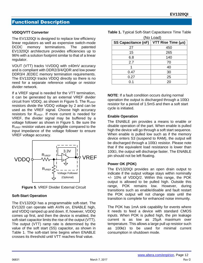
If a VREF signal is needed for the VTT termination, it can be generated by an external VREF divider circuit from VDDQ, as shown in Figure 5. The RVREF resistors divide the VDDQ voltage by 2 and can be used as the VREF signal. Choose high accuracy resistors for RVREF. If more current is needed for VREF, the divider signal may be buffered by a voltage follower as shown in Figure 5. Be sure the RVREF resistor values are negligible compared to the input impedance of the voltage follower to ensure VREF voltage accuracy.
RVREF
RVREF
VREFVDDQ +
-3.3V
Voltage Follower
(Optional)
Figure 5. VREF Divider External Circuit
Soft-Start Operation
The EV1320QI has a programmable soft-start. The EV1320 can operate with AVIN on, ENABLE high, and VDDQ ramped up and down. If, however, VDDQ comes up first, and then the device is enabled, the soft-start capacitor limits the rise of the output (VTT). The output (VTT) ramp rate is determined by the value of the soft start (SS) capacitor, as shown in Table 1. The soft-start time begins when ENABLE crosses its threshold until VTT reaches final value.
Table 1. Typical Soft-Start Capacitance Time Table
(No Load)
SS Capacitance (nF) VTT Rise Time (µs)
27 450
15 265
6.8 140
2.7 70
1 40
0.47 30
0.27 25
0.1 20
NOTE: If a fault condition occurs during normal
operation the output is discharged through a 100 resistor for a period of 1.5mS and then a soft start cycle is initiated.
Enable Operation
The ENABLE pin provides a means to enable or disable operation of the part. When enable is pulled high the device will go through a soft start sequence. When enable is pulled low such as if the memory device enters S3 (suspend to RAM), the output will
be discharged through a 100 resistor. Please note that if the equivalent load resistance is lower than
100, the output will discharge faster. The ENABLE pin should not be left floating.
Power OK (POK)
The EV1320QI provides an open drain output to indicate if the output voltage stays within nominally +/- 10% of VDDQ/2. Within this range, the POK output is allowed to be pulled high. Outside this range, POK remains low. However, during transitions such as enable/disable and fault restart the POK output will not change state until the transition is complete for enhanced noise immunity. The POK has 1mA sink capability for events where it needs to feed a device with standard CMOS inputs. When POK is pulled high, the pin leakage current is as low as 25µA maximum over temperature. This allows a large pull up resistor such
as 100k to be used for minimal current consumption in shutdown mode.

EV1320QI
www.altera.com/enpirion, Page 13
Over-Current Protection
The overload function is achieved by sensing the output voltage. An overload state is entered when the device is out of soft start and the output voltage drops below ~85% of VDDQ/2. When an OCP condition is detected, the device is disabled, the output is discharged through a 100 resistor for a period of 1.5mS. After the 1.5mS discharge time has expired, a soft start is initiated as described in the soft start section. If an over current condition is again detected the device will repeat the discharge/soft start cycle in a hiccup manner as long as the over current condition persists.
Thermal Overload Protection
Thermal shutdown will disable operation when the Junction temperature exceeds approximately 150ºC. Output will discharge through a 100 ohm resistor for 1.5mS. If the thermal fault condition is still present then the device will hiccup until temp falls by 25°C. Once the junction temperature drops by approximately 25ºC, the converter will re-start with a normal soft-start.
Input Under-Voltage Lock-out Internal circuits ensure that the converter will not start switching until the AVIN voltage is above the specified minimum voltage.
EV1320QI
www.altera.com/enpirion, Page 14
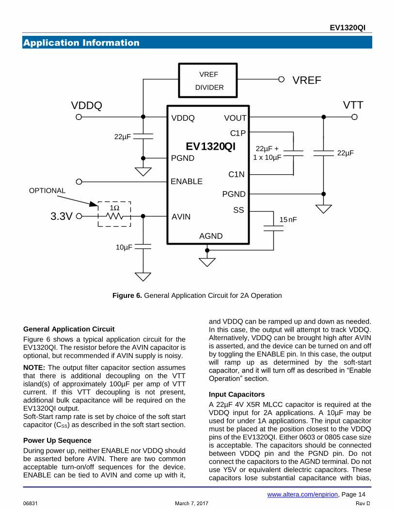
Application Information
VTT
C1P
VOUT
AVIN
AGND
SS
VDDQ
ENABLE
PGND
PGND
C1N
15nF
VDDQ
3.3V
VREF
DIVIDERVREF
EV1320QI
10µF
22µF
22µF +
1 x 10µF22µF
1Ω
OPTIONAL
Figure 6. General Application Circuit for 2A Operation
General Application Circuit
Figure 6 shows a typical application circuit for the EV1320QI. The resistor before the AVIN capacitor is optional, but recommended if AVIN supply is noisy.
NOTE: The output filter capacitor section assumes that there is additional decoupling on the VTT island(s) of approximately 100µF per amp of VTT current. If this VTT decoupling is not present, additional bulk capacitance will be required on the EV1320QI output. Soft-Start ramp rate is set by choice of the soft start capacitor (CSS) as described in the soft start section.
Power Up Sequence
During power up, neither ENABLE nor VDDQ should be asserted before AVIN. There are two common acceptable turn-on/off sequences for the device. ENABLE can be tied to AVIN and come up with it,
and VDDQ can be ramped up and down as needed. In this case, the output will attempt to track VDDQ. Alternatively, VDDQ can be brought high after AVIN is asserted, and the device can be turned on and off by toggling the ENABLE pin. In this case, the output will ramp up as determined by the soft-start capacitor, and it will turn off as described in “Enable Operation” section.
Input Capacitors
A 22µF 4V X5R MLCC capacitor is required at the VDDQ input for 2A applications. A 10µF may be used for under 1A applications. The input capacitor must be placed at the position closest to the VDDQ pins of the EV1320QI. Either 0603 or 0805 case size is acceptable. The capacitors should be connected between VDDQ pin and the PGND pin. Do not connect the capacitors to the AGND terminal. Do not use Y5V or equivalent dielectric capacitors. These capacitors lose substantial capacitance with bias,
EV1320QI
www.altera.com/enpirion, Page 15
frequency, and temperature and are thus not appropriate for use in DCDC converter applications. Refer to the “Layout Recommendation” section for guidance on placement and PCB routing.
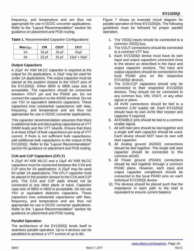
Table 1. Recommended Capacitor Configurations
Max IOUT CIN COUT CFLY
1A 10 µF 10 µF 22µF
2A 22 µF 22 µF 22µF + 10µF
Output Capacitors
A 22µF 4V X5R MLCC capacitor is required at the output for 2A applications. A 10µF may be used for under 1A applications. The output capacitor must be placed at the position closest to the VOUT pins of the EV1320QI. Either 0603 or 0805 case size is acceptable. The capacitors should be connected between VOUT pin and the PGND pin. Do not connect the capacitors to the AGND terminal. Do not use Y5V or equivalent dielectric capacitors. These capacitors lose substantial capacitance with bias, frequency, and temperature and are thus not appropriate for use in DCDC converter applications.
This capacitor recommendation assumes that there is additional bulk and decoupling capacitance at VTT DIMM leads and the VTT islands. Ensure that there is at least 100µF of bulk capacitance per amp of VTT current. If there is not sufficient bulk capacitance, add additional bulk capacitance to the output of the EV1320QI. Refer to the “Layout Recommendation” section for guidance on placement and PCB routing.
C1N and C1P Capacitors (CFLY)
A 22µF 4V X5R MLCC and a 10µF 4V X5R MLCC capacitors must be connected between the C1N and C1P pins for 2A applications. A 22µF may be used for under 1A applications. The CFLY capacitor must be placed in the position closest to the C1N and C1P pins. The C1N and C1P pads should not be connected to any other plane or trace. Capacitor case size of 0805 or 0603 is acceptable. Do not use Y5V or equivalent dielectric capacitors. These capacitors lose substantial capacitance with bias, frequency, and temperature and are thus not appropriate for use in DCDC converter applications. Refer to the “Layout Recommendation” section for guidance on placement and PCB routing.
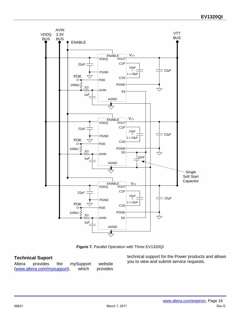
Parallel Operation
The architecture of the EV1320QI lends itself to seamless parallel operation. Up to 4 devices can be paralleled to achieve a VTT current of up to 8A.
Figure 7 shows an example circuit diagram for parallel operation of three EV1320QIs. The following guidelines must be followed for proper parallel operation.
1. The VDDQ inputs should be connected to a common VDDQ bus.
2. The VOUT connections should be connected to a common VTT bus.
3. Each EV1320QI device must have its own input and output capacitors connected close to the device as described in the input and output capacitor sections. The input and output capacitors should be connected to the local PGND pins on the respective EV1320QI devices.
4. The C1N-C1P capacitors should only be connected to their respective EV1320QI devices. They should not be connected to any common bus, VIN, VOUT, or any other signal or plane.
5. All AVIN connections should be tied to a common 3.3V supply rail. Each EV1320QI should have its own AVIN filter resistor and capacitor if required.
6. All ENABLE pins should be tied to a common enable signal.
7. All soft start pins should be tied together and a single soft start capacitor should be used. Each device should NOT have its own soft start capacitor.
8. All Analog ground (AGND) connections should be tied together. The single soft start capacitor should be connected to this common AGND.
9. All Power ground (PGND) connections should be tied together through a common PGND plane. However, each input and output capacitor compliment should be connected to the local PGND pins on each individual EV1320QI device.
10. The devices should be placed such that the impedance in each path to the load is equivalent to ensure current balance.
EV1320QI
www.altera.com/enpirion, Page 16
VTT
C1P
VOUT
AVIN
AGND
SS
VDDQENABLE
PGND
PGND
C1NPOK
100k1
POK
1µF
VTT
C1P
VOUT
AVIN
AGND
SS
VDDQENABLE
PGND
PGND
C1NPOK
100k1
POK
1µF
VTT
C1P
22µF
22µF
VOUT
AVIN
AGND
SS
VDDQENABLE
PGND
PGND
C1N
15nF
22µF+
1 x 10µF
AVIN
3.3V
BUS
POK
100k1
POK
1µF
ENABLE
VDDQ
BUS
VTT
BUS
Single
Soft Start
Capacitor
22µF
22µF
22µF
22µF
22µF+
1 x 10µF
22µF+
1 x 10µF
Figure 7. Parallel Operation with Three EV1320QI
Technical Suport
Altera provides the mySupport website (www.altera.com/mysupport), which provides
technical support for the Power products and allows you to view and submit service requests.
EV1320QI
www.altera.com/enpirion, Page 17
Thermal Considerations
Thermal considerations are important physical limitations that cannot be avoided in the real world. Whenever there are power losses in a system, the heat that is generated by the power dissipation needs to be accounted for.
The Altera Enpirion EV1320QI VDDQ/VTT Converter is packaged in a 3x3x0.55mm 16-pin QFN package. The recommended maximum junction temperature for continuous operation is 125°C. Continuous operation above 125°C may reduce long-term reliability. The device has a thermal overload protection circuit designed to turn off the device at an approximate junction temperature value of 150°C.
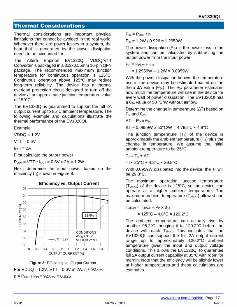
The EV1320QI is guaranteed to support the full 2A output current up to 85°C ambient temperature. The following example and calculations illustrate the thermal performance of the EV1320QI.
Example:
VDDQ = 1.2V
VTT = 0.6V
IOUT = 2A
First calculate the output power.
POUT = VTT * IOUT = 0.6V x 2A = 1.2W
Next, determine the input power based on the efficiency (η) shown in Figure 8.
Figure 8: Efficiency vs. Output Current
For VDDQ = 1.2V, VTT = 0.6V at 2A, η ≈ 92.6%
η = POUT / PIN = 92.6% = 0.926
PIN = POUT / η
PIN ≈ 1.2W / 0.926 ≈ 1.2959W
The power dissipation (PD) is the power loss in the system and can be calculated by subtracting the output power from the input power.
PD = PIN – POUT
≈ 1.2959W – 1.2W ≈ 0.0959W
With the power dissipation known, the temperature rise in the device may be estimated based on the theta JA value (θJA). The θJA parameter estimates how much the temperature will rise in the device for every watt of power dissipation. The EV1320QI has a θJA value of 50 ºC/W without airflow.
Determine the change in temperature (ΔT) based on PD and θJA.
ΔT = PD x θJA
ΔT ≈ 0.0959W x 50°C/W = 4.795°C ≈ 4.8°C
The junction temperature (TJ) of the device is approximately the ambient temperature (TA) plus the change in temperature. We assume the initial ambient temperature to be 25°C.
TJ = TA + ΔT
TJ ≈ 25°C + 4.8°C ≈ 29.8°C
With 0.0959W dissipated into the device, the TJ will be 29.8°C.
The maximum operating junction temperature (TJMAX) of the device is 125°C, so the device can operate at a higher ambient temperature. The maximum ambient temperature (TAMAX) allowed can be calculated.
TAMAX = TJMAX – PD x θJA
≈ 125°C – 4.8°C ≈ 120.2°C
The ambient temperature can actually rise by another 95.2°C, bringing it to 120.2°C before the device will reach TJMAX. This indicates that the EV1320QI can support the full 2A output current range up to approximately 120.2°C ambient temperature given the input and output voltage conditions. This allows the EV1320QI to guarantee full 2A output current capability at 85°C with room for margin. Note that the efficiency will be slightly lower at higher temperatures and these calculations are estimates.
80
82
84
86
88
90
92
94
96
0 0.2 0.4 0.6 0.8 1 1.2 1.4 1.6 1.8 2
EF
FIC
IEN
CY
(%
)
OUTPUT CURRENT (A)
Efficiency vs. Output Current
VTT = 0.6V
CONDITIONSAVIN = 3.0V
VDDQ = 2* VTT
92.6%
EV1320QI
www.altera.com/enpirion, Page 18
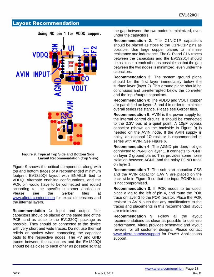
Layout Recommendation
Figure 9: Typical Top Side and Bottom Side
Layout Recommendation (Top View)
Figure 9 shows the critical components along with top and bottom traces of a recommended minimum footprint EV1320QI layout with ENABLE tied to VDDQ. Alternate enabling configurations, and the POK pin would have to be connected and routed according to the specific customer application. Please see the Gerber files at www.altera.com/enpirion for exact dimensions and the internal layers.
Recommendation 1: Input and output filter capacitors should be placed on the same side of the PCB, and as close to the EV1320QI package as possible. They should be connected to the device with very short and wide traces. Do not use thermal reliefs or spokes when connecting the capacitor pads to the respective nodes. The +V and GND traces between the capacitors and the EV1320QI should be as close to each other as possible so that
the gap between the two nodes is minimized, even under the capacitors.
Recommendation 2: The C1N-C1P capacitors should be placed as close to the C1N-C1P pins as possible. Use large copper planes to minimize resistance and inductance. The C1P and C1N traces between the capacitors and the EV1320QI should be as close to each other as possible so that the gap between the two nodes is minimized, even under the capacitors.
Recommendation 3: The system ground plane should be the first layer immediately below the surface layer (layer 2). This ground plane should be continuous and un-interrupted below the converter and the input/output capacitors.
Recommendation 4: The VDDQ and VOUT copper are paralleled on layers 3 and 4 in order to minimize overall series resistance. Please see Gerber files.
Recommendation 5: AVIN is the power supply for the internal control circuits. It should be connected to the 3.3V bus at a quiet point. A 10µF bypass capacitor (shown on the backside in Figure 9) is needed on the AVIN node. If the AVIN supply is noisy, an optional 1Ω resistor is recommended in series with AVIN. See Figure 6.
Recommendation 6: The AGND pin does not get connected to PGND on layer 1. It connects to PGND on layer 2 ground plane. This provides some noise isolation between AGND and the noisy PGND trace on layer 1.
Recommendation 7: The soft-start capacitor CSS and the AVIN capacitor CAVIN are placed on the back side in Figure 9 so that the input PGND trace is not compromised.
Recommendation 8: If POK needs to be used, place a via to the left of pin 4, and route the POK trace on layer 3 to the POK resistor. Place the POK resistor to AVIN such that any modifications to the traces and placements in this recommended layout are minimized.
Recommendation 9: Follow all the layout recommendations as close as possible to optimize performance. Altera provides schematic and layout reviews for all customer designs. Please contact www.altera.com/mysupport for Power Applications support.
EV1320QI
www.altera.com/enpirion, Page 19
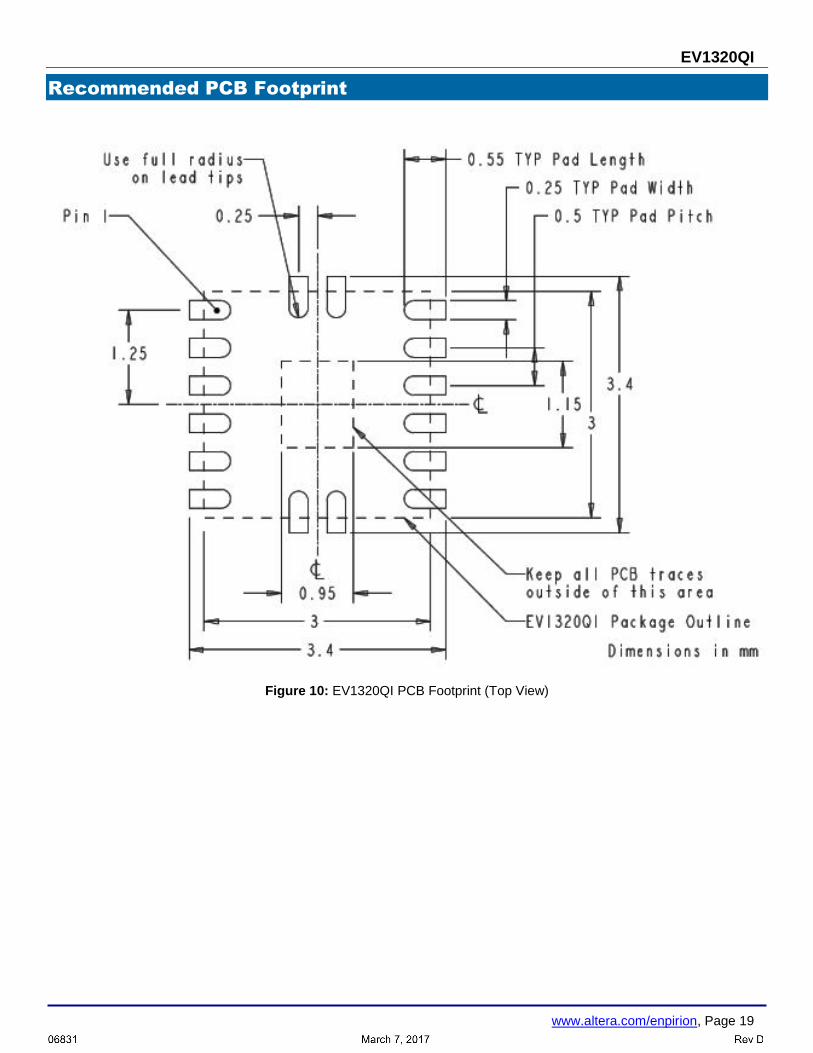
Recommended PCB Footprint
Figure 10: EV1320QI PCB Footprint (Top View)
EV1320QI
www.altera.com/enpirion, Page 20
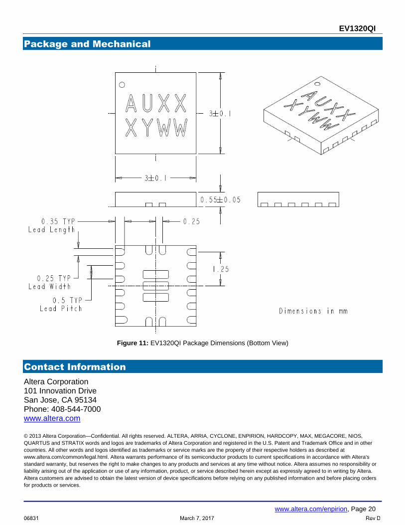
Package and Mechanical
Figure 11: EV1320QI Package Dimensions (Bottom View)
Contact Information
Altera Corporation 101 Innovation Drive San Jose, CA 95134 Phone: 408-544-7000 www.altera.com
© 2013 Altera Corporation—Confidential. All rights reserved. ALTERA, ARRIA, CYCLONE, ENPIRION, HARDCOPY, MAX, MEGACORE, NIOS,
QUARTUS and STRATIX words and logos are trademarks of Altera Corporation and registered in the U.S. Patent and Trademark Office and in other
countries. All other words and logos identified as trademarks or service marks are the property of their respective holders as described at
www.altera.com/common/legal.html. Altera warrants performance of its semiconductor products to current specifications in accordance with Altera's
standard warranty, but reserves the right to make changes to any products and services at any time without notice. Altera assumes no responsibility or
liability arising out of the application or use of any information, product, or service described herein except as expressly agreed to in writing by Altera.
Altera customers are advised to obtain the latest version of device specifications before relying on any published information and before placing orders
for products or services.