xilinx ds567 logicore ip memory controller for … march 1, 2011 5 product specification logicore ip...
TRANSCRIPT

DS567 March 1, 2011 www.xilinx.com 1Product Specification
© 2008-2011 Xilinx, Inc. XILINX, the Xilinx logo, Virtex, Spartan, ISE and other designated brands included herein are trademarks of Xilinx in the United States and other countries. The PowerPC name and logo are registered trademarks of IBM Corp. and are used under license. All other trademarks are the property of their respective owners.
IntroductionThis data sheet describes the LogiCORE™ IP DDR2Memory Controller reference design for the PowerPC®
440 processor block embedded in the Virtex-5 FXTPlatform FPGAs. The processor block interfaces withthe Memory Controller Interface (MCI) and providesthe control interface for DDR2 memory.
Features• Supports a maximum performance of 333 MHz in
the fastest speed grade
• Supports 16-bit, 32-bit, and 64-bit data widths, and 72-bit data width with ECC (DQ:DQS = 8:1)
• Supports DDR2 SDRAM single-rank registered DIMMs and components
• Supports the following DDR2 SDRAM features:
• CAS latencies (3, 4, 5)
• Additive latencies (0, 1, 2, 3, 4)
• On-die termination (ODT)
• Burst lengths (4, 8)
• Supports bank management (up to four banks open)
• Performs the memory device initialization sequence upon power-up
• Performs auto-refresh cycles
LogiCORE IP DDR2 MemoryController for PowerPC 440
Processors (v3.00c)DS567 March 1, 2011 Product Specification
LogiCORE IP Facts
Core Specifics
Supported Device Family (1) Virtex-5
Resources Used See Table 9.
Special Features None
Provided with Core
Documentation Product Specification
Design File Formats Verilog
Constraints File UCF - in EDK Pcore Directory
Verification Verilog Test Bench
Instantiation Template Verilog Wrapper
Additional Items None
Design Tool Requirements
Xilinx Implementation Tools ISE® 12.1
Verification Mentor Graphics® ModelSim® v6.5c and above
Simulation Mentor Graphics ModelSim v6.5c and above
Synthesis Synopsys® Synplify Pro® D-2009.12
Support
Provided by Xilinx, Inc.
1. For a complete list of supported devices, see the 12.1 release notes for this core.
LogiCORE IP DDR2 Memory Controller for PowerPC 440 Processors (v3.00c)
2 www.xilinx.com DS567 March 1, 2011Product Specification
Functional DescriptionThe PPC440MC DDR2 Memory Controller interfaces directly to the PowerPC processor through the MCI (seeFigure 1). To achieve hardware functionality and maximum performance with the memory controller interface, usethe relevant optimal UCF provided in the EDK PCORE directory. There is only one optimal UCF for eachdevice/package/processor combination.
I/O SignalsThe PPC440MC DDR2 Memory Controller signals are listed and described inTable 1.
X-Ref Target - Figure 1
Figure 1: PPC440 MCI and PPC440MC DDR2 Memory Controller Block Diagram
Table 1: PPC440MC DDR2 Memory Controller I/O Signal Description
Signal Name Interface Signal Type
Initial Status Description
PPC440 MCI Signals
MIMCREADNOTWRITE MCI I This signal indicates if the operation is a read or a write.
MIMCADDRESS[0:35] MCI I Address bus
MIMCADDRESSVALID MCI I When asserted, this signal indicates the data on the address bus is valid.
MIMCWRITEDATA[0:127] MCI I Data bus
MIMCBYTEENABLE[0:15] MCI I Byte enable for the data on the data bus
MIMCWRITEDATAVALID MCI I When asserted, this signal indicates the data on the data bus is valid.
MIMCBANKCONFLICTMCI I
This signal is asserted if the bank being accessed is different from the bank accessed in the previous command.
Virtex-5 Embedded Processor Block
PowerPC 440Processor
ICURDAPUControl
FCMInterface
LocalLink0
LocalLink1
LocalLink2
LocalLink3
SPLB0
SPLB1
MPLB
MemoryControllerInterface
PPC440MCDDR Memory
Controller
ControlInterface
DCRInterface
DMA
DMA
DMA
MCI
DMA
CPM/Control
DCR
DCURD
DCUWR
DS567_01_041910

DS567 March 1, 2011 www.xilinx.com 3Product Specification
LogiCORE IP DDR2 Memory Controller for PowerPC 440 Processors (v3.00c)
MIMCROWCONFLICTMCI I
This signal is asserted if the row being accessed is different from the row accessed in the previous command.
MCMIREADDATA[0:127] MCI O Read data bus
MCMIREADDATAVALID MCI O When asserted, this signal indicates the data on the read data bus is valid.
MCMIREADDATAERR MCI O This signal is asserted when an uncorrectable error is detected by the ECC logic.
MCMIADDRREADYTOACCEPT MCI O This signal is asserted when the PPC440MC DDR2 Memory Controller is ready to accept transactions.
DDR2 Signals
DDR2_DQ(C_DDR_DWIDTH – 1:0) DDR2 I/O DDR2 data bus
DDR2_DQS(C_DDR_DQS_WIDTH – 1:0) DDR2 I/O DDR2 data strobe
DDR2_DQS_N(C_DDR_DQS_WIDTH – 1:0) DDR2 I/O DDR2 inverted data strobe
DDR2_A(C_DDR_RAWIDTH – 1:0) DDR2 O DDR2 address
DDR2_BA(C_DDR_BAWIDTH – 1:0) DDR2 O DDR2 bank address
DDR2_RAS_N DDR2 O DDR2 row address strobe
DDR2_CAS_N DDR2 O DDR2 column address strobe
DDR2_WE_N DDR2 O DDR2 write enable
DDR2_CS_N(C_NUM_RANKS_MEM – 1 down to 0)
DDR2 ODDR2 chip selects
DDR2_ODT(C_DDR2_ODT_WIDTH – 1:0) DDR2 O DDR2 ODT enable signal
DDR2_CKE(C_DDR2_NUM_RANKS_MEM– 1:0)
DDR2 ODDR2 clock enable signal
DDR2_DM(C_DDR_DM_WIDTH – 1:0) DDR2 O DDR2 data mask
DDR2_CK(C_NUM_CLK_PAIRS – 1:0) DDR2 O DDR2 clock
DDR2_CK_N(C_NUM_CLK_PAIRS – 1:0) DDR2 O DDR2 inverted clock
System Clock and Reset Signals
MC_MIBCLK CLK I Clock
MI_MCCLK90 CLK I MC_MIBCLK phase shifted by 90
MI_MCCLKDIV2 CLK I MC_MIBCLK divided by 2
MI_MCCLK_200 CLK I IDELAY reference clock
MI_MCRESET RST I Reset
Table 1: PPC440MC DDR2 Memory Controller I/O Signal Description (Cont’d)
Signal Name Interface Signal Type
Initial Status Description

LogiCORE IP DDR2 Memory Controller for PowerPC 440 Processors (v3.00c)
4 www.xilinx.com DS567 March 1, 2011Product Specification
PPC440MC DDR2 Memory Controller Design ParametersTo create a uniquely tailored PPC440MC DDR2 Memory Controller, certain parameterizable features in thePPC440MC DDR2 Memory Controller design allow a design that only utilizes the resources required by the systemand runs at the best possible performance. Table 2 lists the parameterizable features in the PPC440MC DDR2Memory Controller
.
IDELAY_CTRL_RDY_I
FPGA I
Used to daisy chain to downstream IDELAYCTRL when sharing IDELAYCTRLs between multiple pcores. This input port must be tied to "1" when not sharing IDELAYCTRLs.
IDELAY_CTRL_RDYFPGA O
This output from an upstream IDELAYCTRL pcore connects to the downstream IDELAY_CTRL_I input port when sharing IDELAYCTRLs between multiple pcores.
Table 2: PPC440MC DDR2 Memory Controller Design Parameters
Feature/Description Parameter Name Allowable Values Default Value
PPC440MC DDR2 Memory Controller Features
Base Address for Memory C_MEM_BASEADDR 32’hFFFFFFFF
High Address for Memory C_MEM_HIGHADDR 32’h00000000
CPMINTERCONNECTCLK to PPC440MC DDR2 clock ratio
C_MIB_MC_CLOCK_RATIO 0 or 1 for 1:1, 2:1, or 3:1clock ratios2 for 3:2 clock ratio
0
DDR2 clock period (tCK) in ps C_MC_MIBCLK_PERIOD_PS 3000 to 8000 3000
Number of generated clock pairs supplied to the DDR2 memory
C_NUM_CLK_PAIRS 1 to 5 1
Supported number of external DDR2 memory ranks
C_NUM_RANKS_MEM 1 1
Include ECC Logic C_INCLUDE_ECC_SUPPORT 0 = Disable1 = Enable 0
DDR2 Features
DDR2 Data Width C_DDR_DWIDTH (1) 16, 32, 64, 72 64
DDR2 Strobe Width C_DDR_DQS_WIDTH 2, 4, 8, 9 8
DDR2 Data Mask Width C_DDR_DM_WIDTH 2, 4, 8, 9 8
DDR2 Row Address Width C_DDR_RAWIDTH All supported memory row address widths 14
DDR2 Column Address Width C_DDR_CAWIDTH All supported memory column address widths 10
DDR2 Bank Address Width C_DDR_BAWIDTH 2, 3 2
DDR2 CAS Latency C_DDR_CAS_LAT (2) 3, 4, 5 5
DDR2 Burst Length C_DDR_BURST_LENGTH (3) 4, 8 4
DDR2 is a registered DIMM C_REG_DIMM 0 = Unbuffered memory1 = Registered memory
0
Table 1: PPC440MC DDR2 Memory Controller I/O Signal Description (Cont’d)
Signal Name Interface Signal Type
Initial Status Description
DS567 March 1, 2011 www.xilinx.com 5Product Specification
LogiCORE IP DDR2 Memory Controller for PowerPC 440 Processors (v3.00c)
On Die Termination Selection C_DDR2_ODT_SETTING 0 = Disables ODT1 = ODT enabled, RTT = 75Ω2 = ODT enabled, RTT = 150Ω3 = ODT enabled, RTT = 50Ω
1
DDR2 ODT Width C_DDR2_ODT_WIDTH 0 to 4 1
DDR2 Additive Latency C_DDR2_ADDT_LAT 0 to 4 0
Delay after ACTIVE command before READ/WRITE command (ps)
C_DDR_TRCD 15000
Delay after ACTIVE command before PRECHARGE command (ps)
C_DDR_TRAS 40000
Delay after PRECHARGE command (ps) C_DDR_TRP 15000
Delay after AUTOREFRESH before another command (ps)
C_DDR_TRFC 70000
Read to PRECHARGE command delay (ps) C_DDR_TRTP 7500
Write Recovery Time (ps) C_DDR_TWR 15000
Write-to-Read Command Delay (ps) C_DDR_TWTR 10000
Average periodic refresh command interval (ns)
C_DDR_TREFI 7800
Skip 200 µs power up delay for simulation C_SIM_ONLY 0, 1 0
IDELAY high-performance mode C_IDEL_HIGH_PERF TRUE, FALSE TRUE
log2 of C_DQS_WIDTH C_DQS_BITS — 3
log2 of C_DDR_DWIDTH C_DQ_BITS — 6
log2 of C_NUM_RANKS_MEM C_CS_BITS — 0
Optional pipeline stage in read data path
C_READ_DATA_PIPELINE 0 or 1 0
Number of IDELAYCTRLs internally generated C_NUM_IDELAYCTRL - 1
Reduces drive strength of DDR2 SDRAM I/O when set to 1
C_REDUCE_DRV 0,1 0
Applies IODELAY_GROUP constraint to all IDELAYCTRL and all IDELAY instances in pcore
C_IODELAY_GRPSTRING <InstanceName>
FPGA device speed grade required for predictable IP
C_FPGA_SPEED_GRADE 1,2, 3 2
1. – MCI burst width of 32 for DDR2 data width of 16– MCI burst width of 64 for DDR2 data width of 32– MCI burst width of 128 for DDR2 data width of 64/72
2. When the parameter C_DDR_CAS_LAT is set to 3, the user must set the C_DDR2_ADDT_LAT parameter to any value from 1 to 4.3. – MCI burst length of 2 for DDR2 burst length of 4
– MCI burst length of 4 for DDR2 burst length of 8
Table 2: PPC440MC DDR2 Memory Controller Design Parameters (Cont’d)
Feature/Description Parameter Name Allowable Values Default Value

LogiCORE IP DDR2 Memory Controller for PowerPC 440 Processors (v3.00c)
6 www.xilinx.com DS567 March 1, 2011Product Specification
Allowable Parameter Combinations
The PPC440MC DDR2 Memory Controller allows one external rank of memory. Individual rank address ranges arecalculated by C_MEM_BASEADDR and C_MEM_HIGHADDR. The ranges must comprise a complete, contiguouspower of two range such that range = 2m, and the m least-significant bits of C_MEM_BASEADDR must be zero.
All external memory ranges are calculated contiguous to each other in the system addressable space. In addition, allexternal memory ranks are identical in size to other ranks of memory space.
Parameter - Port Dependencies
Table 3 illustrates the port and parameter dependencies. With the configuration flexibility of the channelized accessmemory controller, the user must be aware of unused I/Os based on the configuration of each port. The designermust also be aware of the external memory interface signals based on the type of memory utilized in the system.
Table 3: Parameter-Port Dependencies
Name Affects Depends Relationship Description
Design Parameters
C_NUM_CLK_PAIRS DDR_Clk, DDR_Clkn Affects size of signals.
C_NUM_RANKS_MEM DDR_CKE, DDR_CSn, DDR_ODT, C_MEM_BASEADDR, C_MEM_HIGHADDR
Affects size of signals.
C_DDR_DWIDTH DDR_DQ Parameter affects size of DDR DQ signals.
C_DDR_DQS_WIDTH DDR_DQS,DDR_DQS_N
Parameter affects size of DDR DQS signals.
C_DDR_DM_WIDTH DDR_DM Parameter affects size of DDR DM signals.
C_DDR_RAWIDTH DDR_Addr Affects size of signal.
C_DDR_BAWIDTH DDR_BankAddr Affects size of signal.
I/O Signals
DDR_Clk, DDR_Clkn C_NUM_CLK_PAIRS Size depends on C_NUM_CLK_PAIRS parameter.
DDR_CKE, DDR_CSn C_NUM_RANKS_MEM Size depends on C_NUM_RANKS_MEM parameter.
DDR_DQ C_DDR_DWIDTH Size depends on parameter setting.
DDR_DQS C_DDR_DQS_WIDTH Size depends on parameter setting.
DDR_DM C_DDR_DM_WIDTH Size depends on parameter setting.
DDR_Addr C_DDR_RAWIDTH Size depends on parameter setting.
DDR_BankAddr C_DDR_BAWIDTH Size depends on parameter setting.
DDR_DQS_N, DDR_ODT
C_NUM_MEM_RANKS Size depends on parameter setting.
DS567 March 1, 2011 www.xilinx.com 7Product Specification
LogiCORE IP DDR2 Memory Controller for PowerPC 440 Processors (v3.00c)
Connecting to MemoryDDR2 SDRAM accesses can be halfword (two bytes), word (four bytes), or doubleword (eight bytes), depending onthe user configuration. Data to and from the MCI to the PPC440MC DDR2 Memory Controller is organized as big-Endian (D[0:63], D0 is the MSB). The PPC440MC DDR2 Memory Controller is organized as little-Endian (D[63:0],D63 is the MSB). Table 4 shows the interconnection from the MCI to the PPC440MC DDR2 Memory Controller andfrom the PPC440MC DDR2 Memory Controller to the DDR2 memory.
Memory Part Parameter Considerations
Many parameters of the PPC440MC DDR2 Memory Controller must be set according to the memory device usedfor proper operation. These parameters include control port widths and memory timing specifications. The valuesfor these parameters can usually be found in memory vendor data sheets or other documentation though may belabeled slightly differently.
MIG PHY UCF and MHS ConsiderationsThis core utilizes the MIG controller PHY to calibrate memory. The MIG PHY requires a set of pinout-specificplacement and timing constraints to operate. Special handling of IDELAYCTRLs may also be necessary whenmultiple IDELAY-enabled IP cores share an I/O bank and clock region.
Using Optimal Pinouts
This sections details designs that use the recommended high performance pinouts provided in<EDK_Install_Dir>/hw/XilinxProcessorIPLib/pcores/ppc440mc_ddr2_<version>/data/ppc440mc_ddr2_ucfs.
1. Choose the applicable predefined UCF from the directory above. The UCF file names are organized in the following order: maximum total memory DQ width, part name, part package, and I/O banks occupied. Multiple UCFs are provided in some part/package combinations to support both PPC440 processors.
2. Copy the predefined UCF into the project UCF file, often named data/system.ucf.
3. If necessary, modify the instance names of the copied UCF to match top-level port names.
4. If necessary, modify the hierarchy of the copied UCF constraints to match the actual design hierarchy. Specifically, "u_ddr2_top" will need to be modified to the instance name of the PPC440MC_DDR2 core name, perhaps with a "*" wildcard added to the start of the name to match additional user design hierarchy.
Table 4: MCI to PPC440MC DDR2 to DDR2 Signal Connections
Description MCI to PPC440MC DDR2 Signal [MSB:LSB] PPC440MC DDR2 to DDR2 Signal [MSB:LSB]
Data BusMIMCWRITEDATA[0:(C_DDR_DWIDTH * 2) – 1]MCMIREADDATA[0:(C_DDR_DWIDTH * 2) – 1]
DDR2_DQ[C_DDR_DWIDTH – 1:0]
Address Bus MIMCADDRESS[0:35] DDR2_A[C_DDR_AWIDTH – 1:0]
Bank Address Memory Controller Generated DDR2_BA[C_DDR_BAWIDTH – 1:0]
Data Strobe Memory Controller Generated DDR2_DQS[(C_DDR_DWIDTH/C_DDR_DQS_WIDTH) – 1:0]
Data Mask MIMCBYTEENABLE[0:(C_MIBDATA_WIDTH/8) – 1] DDR2_DM[(C_DDR_DWIDTH/C_DDR_DM_WIDTH) – 1:0]

LogiCORE IP DDR2 Memory Controller for PowerPC 440 Processors (v3.00c)
8 www.xilinx.com DS567 March 1, 2011Product Specification
Using Custom MIG-Compatible Pinouts
It is strongly recommended to use the provided I/O pinouts for optimal performance. However, MIG-compatiblecustom pinouts can be generated and used with the PPC440MC_DDR2 core. To use a custom pinout, the MIG"Update Design" flow must be followed to generate the required UCF and MHS constraints. The steps are:
1. A MIG 3.2 project must be generated through Xilinx CORE Generator GUI. MIG is located in the "Memories & Storage Elements->Memory Interface Generators" section. To access all available MIG versions, select the "All IP Versions" check box in the Xilinx CORE Generator GUI. Note: Because the desired pinout is already available, all banks can be selected in the MIG bank selection screen.
2. If the default MIG pinout generated in <MIG Project>/user_design/par/ddr2_sdram.ucf is not the desired pinout, run the MIG > Update Design flow using the MIG project and a UCF with the desired pinout in a MIG-formatted UCF. Note: The input UCF parsing to the MIG > Update Design flow currently requires strict adherence to the formatting similar to MIG UCF output for complete Update Design UCF parsing. Warnings in this step relating to missing pins in the UCF can be ignored if similar pins are not used by the PPC440MC_DDR2 core. For example the clk200_p, clk200_n, sys_rst_n, phy_init_done, and extra ddr2_cs_n, ddr2_odt, ddr2_ck, and ddr_ck_n ports can be ignored during this step.
3. Copy the generated MIG UCF from <MIG Project>/user_design/par/ddr2_sdram.ucf into the project UCF file, often named data/system.ucf. The following steps involving UCFs will modify this file.
4. If necessary, modify the instance names of the copied UCF to match top-level port names.
5. In the UCF, rename "u_usr_rd" to "usr_rd" in the following line: INST "*/u_usr_rd/gen_rden_sel_mux*.u_ff_rden_sel_mux" TNM = "TNM_RDEN_SEL_MUX";
6. The maximum memory speed of a custom pinout is generally determined by static timing analysis, up to 333MHz in the fastest speed grade. To improve timing results, the C_READ_DATA_PIPELINE MHS parameter may need to be set to '1'.
More information on the MIG Update Design flow can be found in the MIG documentation, and in Xilinx Answer29313.
Multiple PPC440MC_DDR2 Controllers
When using 2 PPC440MC_DDR2 controllers in a single FPGA, a pinout-specific UCF is required for each controller.In addition, all of the instance names, time groups, and TIMESPECS in the project UCF must be made unique toeach controller. For the instance (INST) portion of each constraint, an additional level of hierarchy can be added tothe start of the instance name. The time group (TNM) and TIMESPEC constraints must also be given unique labels.For example, the following constraints for a controller instance name 'dimm0' could be changed from:
INST "*/u_phy_calib/gen_rd_data_sel*.u_ff_rd_data_sel" TNM = "TNM_RD_DATA_SEL";
TIMESPEC "TS_MC_RD_DATA_SEL" = FROM "TNM_RD_DATA_SEL" TO FFS
"TS_SYS_CLK" * 4;
To:
INST "*/dimm0*/u_phy_calib/gen_rd_data_sel*.u_ff_rd_data_sel" TNM = "TNM_RD_DATA_SEL_DIMM0";
TIMESPEC "TS_MC_RD_DATA_SEL_DIMM0" = FROM "TNM_RD_DATA_SEL_DIMM0" TO FFS
"TS_SYS_CLK" * 4;
Similar changes must be made to all other constraints for each controller UCF.
DS567 March 1, 2011 www.xilinx.com 9Product Specification
LogiCORE IP DDR2 Memory Controller for PowerPC 440 Processors (v3.00c)
IDELAYCTRL Shared Pinout ConsiderationsNote: When the PPC440MC_DDR2 does not have I/O locations in the same clock region as another IP core which uses IODELAYs, this section can be ignored. In Virtex-5, I/O banks fully contain multiple clock regions, so that I/O in different banks also exist in different clock regions. This makes a simple test of a pinout to check for the non-sharing of clock regions.
To utilize the dynamic delay elements available in Virtex-5, the PPC440MC_DDR2 uses IODELAY andIDELAYCTRL elements to improve read timing margin. Multiple other Xilinx IP cores and user custom logic alsoutilize IODELAY and IDELAYCTRL elements which may need to be coordinated with the PPC440MC_DDR2 core.Single PPC440MC_DDR2 designs or multiple cores whose I/O do not share clock regions are automaticallyhandled by the Xilinx implementation tools and do not require this section.
A single IDELAYCTRL element calibrates all IODELAYs in a clock region. When another IODELAY-enabled IP coreshares the clock region with the PPC440MC_DDR2 core I/O for its pin placement, a single IDELAYCTRL must beshared between both cores. This can be accomplished by allowing a single "master" core to instantiate theIDELAYCTRL which the other "slaves" utilize. The slave cores must not instantiate any IDELAYCTRLs. The mastercore outputs the RDY signal from its instantiated IDELAYCTRL which the slaves can optionally use to trigger tostart their use of their IODELAYs after FPGA programming or IDELAYCTRL reset. Sharing of IDELAYCTRLs aresignified to the implementation tools by all shared IP cores having the same IODELAY_GROUP constraint value onall of their IDELAYCTRL and IODELAY elements. The PPC440MC_DDR2 provides the C_IODELAY_GRP andC_NUM_IDELAYCTRL parameters and IDELAY_CTRL_RDY_I and IDELAY_CTRL_RDY ports to provide thisfunctionality.
I/O Clock Region Sharing Rules1. - All IDELAYCTRL and IDELAY elements must have the same IODELAY_GROUP constraint value. This is
provided by setting the PPC440MC_DDR2 C_IODELAY_GRP MHS parameter. Other cores which do not provide explicit top-level IODELAY_GROUP parameters may be set with IODELAY_GROUP constraints on all IDELAYCTRL and IODELAYs instantiated by the core in the UCF file. By default EDK sets the C_IODELAY_GRP parameter of each PPC440MC_DDR2 to the unique instance name in the MHS, generally allowing single or non-shared clock region pinouts between multiple cores to function without any special handling.
2. - Only one IP core should have IDELAYCTRLs instantiated within it. The PPC440MC_DDR2 provides this with the C_NUM_IDELAYCTRL MHS parameter. Setting to '0' will prevent the instantiation of an IDELAYCTRL.
3. - Resetting the IP core which contains the IDELAYCTRLs will affect the IODELAYs of all IP cores in the IODELAY_GROUP. All cores in the group should be reset with the same reset signal.
4. - The PPC440MC_DDR2 provides the IDELAY_CTRL_RDY port as the output AND of all of its IDELAYCTRLs RDY signals and its IDELAY_CTRL_RDY_I input. The IDELAY_CTRL_RDY signal can be consumed by other IP cores that are using the IDELAYCTRL to indicate when IDELAYCTRL calibration is completed and the core can use its IODELAYs.
5. - The PPC440MC_DDR2 provides the IDELAY_CTRL_RDY_I signal to receive the RDY signal from another core's IDELAYCTRL, such as another PPC440MC_DDR2 IDELAY_CTRL_RDY port. The IDELAY_CTRL_RDY_I is AND'd with the internal core reset before allowing memory calibration to begin. The port is defaulted to '1' by the EDK tools when unconnected. Setting to '0' will prevent the PPC440MC_DDR2 from beginning operation.
LogiCORE IP DDR2 Memory Controller for PowerPC 440 Processors (v3.00c)
10 www.xilinx.com DS567 March 1, 2011Product Specification
Shared Clock Region Example
This example MHS excerpt contains the relevant parameters for two PPC440MC_DDR2 cores with I/O portsLOCed to the same bank/clock region. The first memory is the master and provides the RDY signal to the secondcore, which does not have any IDELAYCTRLs generated.
BEGIN ppc440mc_ddr2
PARAMETER INSTANCE = DDR2_SDRAM_DIMM0
PARAMETER C_IODELAY_GRP = MYGRP
PARAMETER C_NUM_IDELAYCTRL = 1
PORT idelay_ctrl_rdy = RDY_MYGRP
END
BEGIN ppc440mc_ddr2
PARAMETER INSTANCE = DDR2_SDRAM_DIMM1
PARAMETER C_IODELAY_GRP = MYGRP
PARAMETER C_NUM_IDELAYCTRL = 0
PORT idelay_ctrl_rdy_i = RDY_MYGRP
END
UCF Constraint Prorating for Slower Clock Frequencies
The optimal constraint files provided with the PPC440MC_DDR2 assume a 333MHz clock speed. When running ata slower memory rate, the UCF constraints can be relaxed to ease timing closure.
PERIOD Constraint
The PERIOD constraint in the UCF should be removed if the memory clock, mc_mibclk, is already covered by anexisting system constraint. This typically occurs when a PERIOD constraint is placed on the system clock input andautomatically propagates through DCMs and PLLs to constrain the memory clock.
Multi-cycle Constraints
The multi-cycle constraints which end in "TS_SYS_CLK" * 4 are dependent on the memory clock frequency. Thetotal value should not exceed 4 memory clock (mc_mibclk) cycles. For simplicity, the "TS_SYS_CLK" * 4 TIMESPECvalue can be replaced with an integer time value corresponding to four memory clock cycles. As an example, a200MHz memory clock design can replace the "TS_SYS_CLK" * 4 clauses with 20ns.
DQS Gate MAXDELAY Constraints
The MAXDELAY constraint involving the "en_dqs_sync" net can have its requirements relaxed based on the actualmemory clock frequency. The following constraint can be prorated if the memory clock is slower than 333MHz:
NET "*/u_phy_io/gen_dqs*.u_iob_dqs/en_dqs_sync" MAXDELAY = 800 ps;
Some examples for "en_dqs_sync" timespec values by clock frequency: 300MHz = 850ps, 267MHz = 900ps and200MHz = 950ps.
Note that the similar "en_dqs" MAXDELAY constraint value should not be modified with frequency.

DS567 March 1, 2011 www.xilinx.com 11Product Specification
LogiCORE IP DDR2 Memory Controller for PowerPC 440 Processors (v3.00c)
PPC440 CPU/MCI ConsiderationsThis section details the connection of the PPC440MC DDR2 Memory Controller to the PPC440 Memory ControllerInterface (MCI) and the PPC440 MCI parameter settings.
PPC440 MCI Bus Connections
Connecting signals between the PPC440MC DDR2 Memory Controller and the PPC440 core instances isaccomplished through a single bus connection, PPC440MC.
PPC440 Clocking
The CPMMCCLK clock port of the PPC440 instance should usually be the same clock as the MC_MIBCLK port ofthe PPC440MC DDR2 Memory Controller.
PPC440 C_PPC440MC_CONTROL Settings
The MI_CONTROL register configures the PPC440 MCI with the correct data widths, latency, burst lengths, androw/bank management behavior. MI_CONTROL is the PPC440 DCR register, while an initial value can beprovided through the C_PPC440MC_CONTROL parameter on the PPC440 MHS instance. Table 5 shows thesuggested bit settings for the C_PPC440MC_CONTROL parameter.
Table 5: C_PPC440PC_CONTROL/MI_CONTROL Register Settings
Bit PPC440 Label Allowable Values
0 enable 1
1 Rowconflictholdenable 1
2 Bankconflictholdenable 1
3 Directionconflictholdenable 1
4:5 Autoholdduration 10
62:3 clock Ratio mode 0 = Integer CPMMCCLK-CPMINTERCONNECTLCK clock ratio
1 = 2:3 CPMMCCLK:CPMINTERCONNCECTCLK clock ratio
7 overlapdwr 0
8:9
Burstwidth Double the DDR memory DQ data width because MCI must provide 2x the DQ width every clock period00 = 128 bit01 = 64 bit11 = 32 bit
10:11
Burstlength Half of C_DDR_BURST_LENGTH as 2x DQ width is transferred each MCI clock cycle01 = C_DDR_BURST_LENGTH set to 410 = C_DDR_BURST_LENGTH set to 8
12:15 Write Data Delay (WDD) 0000
16Read Modify Write (RMW) 0 = Disable ECC. C_INCLUDE_ECC_SUPPORT set to 0
1 = Enable ECC. C_INCLUDE_ECC_SUPPORT set to 1
17:23 Reserved 0000000
24PLB Priority Enable 0 = SPLB0/SPLB1 master priority disabled
1 = SPLB0/SPLB1 master priority enabled (default)
25:27 Reserved 000
28 Pipelined Read Enable 1
LogiCORE IP DDR2 Memory Controller for PowerPC 440 Processors (v3.00c)
12 www.xilinx.com DS567 March 1, 2011Product Specification
Address Mapping
Table 6 shows the address mapping from the MCI interface. The address on the MCI interface maps to a continuousaddress space at the memory. The memory address mapping is determined by the data width of the memory, sinceeach column address maps a location in memory for the width of each data beat.
An address offset is calculated based on the width of the DDR2 data bus. The DDR2 column address locations arecalculated based on the offset, followed by the row address and bank address. Table 7 shows the bit locations for theDDR2 address bus. The address, which is from the MCI, is in big-Endian format.
29 Pipelined Write Enable 1
30:31 Reserved 11
Table 6: Physical Controller Address Mapping
Memory Use Physical Controller Address
Address Offset log2(C_DDR_DWIDTH/8)
Column Address MIMCADDRESS [(C_DDR_CAWIDTH + Address Offset – 1) : Address Offset]
Row Address MIMCADDRESS [(C_DDR_RAWIDTH + C_DDR_CAWIDTH + Address Offset – 1) : (C_DDR_CAWIDTH + Address Offset)]
Bank Address MIMCADDRESS [(C_DDR_BAWIDTH + C_DDR_RAWIDTH + C_DDR_CAWIDTH + Address Offset – 1) : (C_DDR_RAWIDTH + C_DDR_CAWIDTH + Address Offset)]
Table 7: Calculation of Address Bits
Variable Equation
ADDR_OFFSET log2(C_DDR_DWIDTH/8)
COLADDR_STARTBIT MCI_ADDR_WIDTH – (C_DDR_CAWIDTH+ADDR_OFFSET)
COLADDR_ENDBIT COLADDR_STARTBIT + C_DDR_CAWIDTH – 1
ROWADDR_STARTBIT COLADDR_STARTBIT – C_DDR_AWIDTH
ROWADDR_ENDBIT ROWADDR_STARTBIT + C_DDR_AWIDTH – 1
BANKADDR_STARTBIT ROWADDR_STARTBIT – C_DDR_BAWIDTH
BANKADDR_ENDBIT BANKADDR_STARTBIT + C_DDR_BAWIDTH – 1
Table 5: C_PPC440PC_CONTROL/MI_CONTROL Register Settings (Cont’d)
Bit PPC440 Label Allowable Values

DS567 March 1, 2011 www.xilinx.com 13Product Specification
LogiCORE IP DDR2 Memory Controller for PowerPC 440 Processors (v3.00c)
Table 8 shows an example of the address mapping. In this example, the DDR2 data width is 32, the column addresswidth is 9, the row address width is 13, and the bank address width is 2.
Row Conflict and Bank Conflict Mask Settings
The MI_ROWCONFLICT_MASK and MI_BANKCONFLICT_MASK parameters, set by the user, enable thePPC440 Memory Controller Interface (MCI) to detect row address and bank address conflicts between the currentand previous command addresses. MI_ROWCONFLICT_MASK and MI_BANKCONFLICT_MASK parametersmust be set based on the address offset width, the memory device column address width, the memory device rowaddress width, and the memory device bank address width. The address offset width equals log2(C_DDR_DWIDTH/8).
Figure 2 shows the address fields of MIMCADDRESS [0:35], the corresponding 32-bitMI_BANKCONFLICT_MASK, and 32-bit MI_ROWCONFLICT_MASK for a memory interface with the followingparameters.
• C_DDR_DWIDTH = 64
• Address Offset = log2(64/8) = 3
• Column Address Width = 10
• Row Address Width = 14
• Bank Address Width = 3
Table 8: Example Address Mapping (C_DDR_DWIDTH=32, C_DDR_CAWIDTH=9, C_DDR_RAWIDTH=13, C_DDR_BAWIDTH=2)
Variable Equation Value
ADDR_OFFSET log2(C_DDR_DWIDTH/8) log2(32/8) = 2
COLADDR_STARTBIT MCI_ADDR_WIDTH – (C_DDR_CAWIDTH+ADDR_OFFSET) 36 – (9 + 2) = 25
COLADDR_ENDBIT COLADDR_STARTBIT + C_DDR_CAWIDTH – 1 25 + (9 - 1) = 33
ROWADDR_STARTBIT COLADDR_STARTBIT – C_DDR_AWIDTH 25 – 13 = 12
ROWADDR_ENDBIT ROWADDR_STARTBIT + C_DDR_AWIDTH – 1 12 + 13 - 1 = 24
BANKADDR_STARTBIT ROWADDR_STARTBIT – C_DDR_BAWIDTH 12 – 2 = 10
BANKADDR_ENDBIT BANKADDR_STARTBIT + C_DDR_BAWIDTH – 1 10 + 2 – 1 = 11
X-Ref Target - Figure 2
Figure 2: MIMCADDRESS Bus and Corresponding MI_ROWCONFLICT_MASK and MI_BANKCONFLICT_MASK
DS567_02_041910
0 5 6 7 8 9 2223 ......... 32333435
0 0 1 1 1 0
0 5 6 7 8 9
0......31
0 1 1 1 1 1 1 1 1 1 1 1 10 1
0
1 0
22238 9
0......31
10-bit Column Address
14-bit Row Address
3-bit Address Offset
3-bit Bank Address
Unused bits
MI_BANKCONFLICT_MASK = 32’h03800000
MI_ROWCONFLICT_MASK = 32’h007FFE00
LogiCORE IP DDR2 Memory Controller for PowerPC 440 Processors (v3.00c)
14 www.xilinx.com DS567 March 1, 2011Product Specification
MI_ROWCONFLICT_MASK [0:31] corresponds to MIMCADDRESS [0:31] with the Row Address bits set to onesand all other bits set to zeros to enable conflict detection. And the MI_BANKCONFLICT_MASK [0:31] correspondsto MIMCADDRESS [0:31] with the Bank Address bits set to ones and all other bits set to zeros to enable conflictdetection.
Another example with reduced data width:
• C_DDR_DWIDTH = 32
• Address Offset = log2(32/8) = 2
• Column Address Width = 10
• Row Address Width = 14
• Bank Address Width = 3
The MI_ROWCONFLICT_MASK and MI_BANKCONFLICT_MASK parameters are:
• MI_ROWCONFLICT_MASK = 32'h003fff00
• MI_BANKCONFLICT_MASK = 32'h01c00000
Upgrading From PPC440MC_DDR2 v2.00.x to v3To migrate an existing design from PPC440MC_DDR2v2 to PPC440MC_DDR2v3, the following steps are necessary.
Note: Tool errors are reported if the subsequent steps are not performed.
1. In the MHS file, the C_MEM_DQS_IO_COL, C_MEM_DQ_IO_MS, and C_IDELAYCTRL_LOC parameters are no longer used and must be removed from the PPC440MC_DDR2 instance.
2. In the UCF file, PPC440MC_DDR2 specific constraints containing AREA_GROUP and RLOC_ORIGIN must be removed. Also remove any PPC440MC_DDR2 LOC constraints involving IDELAYCTRL_XxYy sites from the UCF.
Design Implementation
FIFOs
The read and write datapaths have FIFOs for storing data. The FIFOs in Virtex-5 FXT devices have a built-in ECCmodule. For applications that require ECC, the ECC in the FIFOs can be used. The block RAMs next to the PPCblock are used to implement these FIFOs.
There is no latency impact during writes. The PPC440MC DDR2 Memory Controller operates with a write datadelay of zero, and the data is in the FIFO when it has to be sent to the memory. For reads, there is a one-cycle latencyhit because of using the FIFOs.
Clocking and Reset
The PPC440MC DDR2 Memory Controller requires all four phases of the clock. The CLK180 and CLK270 signalsare generated by local inversion using MI_MCCLK and MI_MCCLK90. The MI_MCRESET from the MCI module issynchronized to CLK180, CLK270, MI_MCCLK90, and the MI_MCCLK_200 before being used in the design.

DS567 March 1, 2011 www.xilinx.com 15Product Specification
LogiCORE IP DDR2 Memory Controller for PowerPC 440 Processors (v3.00c)
Top-Level Design
The PPC440MC DDR2 Memory Controller is comprised of the controller, the physical layer, and the FIFO interfaceas shown in Figure 3.
Physical Layer
The physical layer is comprised of the write datapath, the read datapath, the calibration state machine for DQS andDQ calibration, the calibration logic for read enable alignment, and the memory initialization state machine. Thewrite datapath generates the data and strobe signals transmitted during a Write command. The read datapathcaptures the read data in the read strobe domain.
Write Datapath
The write datapath, shown in Figure 4, is implemented using the IOB ODDR in the same edge mode. Two datawords are presented on the rising edge of the FPGA clock and the ODDR converts it into DDR data.
X-Ref Target - Figure 3
Figure 3: PPC440MC DDR2 Memory Controller Block Diagram
X-Ref Target - Figure 4
Figure 4: Write Datapath
Physical Layer
Controller
Read/WriteFIFO
DDR2 SDRAM
MC_TOP MCI
DS567_03_041910
Clock, Reset, I/O Control
Write Data Rise D1DQ
ODDR
DS567_04_041910
Write Data Fall
FPGA Clock
D2

LogiCORE IP DDR2 Memory Controller for PowerPC 440 Processors (v3.00c)
16 www.xilinx.com DS567 March 1, 2011Product Specification
Read Datapath
As outlined in XAPP858 High-Performance DDR2 SDRAM Interface in Virtex-5 Devices, the read datapath comprisesseveral flip-flop stages (ranks) over which read data from the DDR2 memory is transferred from the DQS strobedomain to the internal FPGA (CLK0) clock domain. It also includes the local I/O clock network for distributing theDQS for the initial data capture, and circuitry to ensure robust data capture on the last transfer of a read burst:
• Rank 1 Capture: Initial capture of DQ with DQS using the IOB IDDR flip-flop and IDELAY elements. The differential DQS pair must be placed on a clock-capable I/O pair and is distributed through the local BUFIO network to each of the corresponding DQ IDDR capture flip-flops. The IDDR generates two single-data-rate signals at its Q1 and Q2 outputs. Both Q1 and Q2 outputs are clocked by the falling edge of DQS because:
• The IDDR is configured in SAME_EDGE mode.
• The DQS is inverted before clocking the IDDR.
• Rank 2 Capture: The IDDR captures the data from the DDR2 memory, which is in the double-data-rate domain, and generates two single-data-rate streams at its Q1 and Q2 outputs. The outputs of the IDDR are transferred to flip-flops that are clocked by the rising or falling edge of CLK0. These flip-flops are located in the CLBs. There are two possible sets of flip-flops that each IDDR output can be transferred to. This allows synchronization of the IDDR outputs to either edge of CLK0 and reduces the maximum number of IDELAY taps required to perform timing alignment.
• Rank 3 Capture: The output of Rank 2 flip-flops clocked by the falling edge of CLK0 are transferred to flip-flops clocked by the rising edge of CLK0. In addition, the multiplexer for each DQ capture circuit is set to choose the appropriate synchronization path used.
• DQS Gate Circuit: This circuit disables the clock enable for each DQ IDDR at the end of a read burst to prevent any glitches associated with the DQS strobe being 3-stated by the memory from clocking the IDDR flip-flop. There is one such circuit per DQS group.
The read datapath is shown in Figure 5.X-Ref Target - Figure 5
Figure 5: Read Datapath
DQ
DQS
IDELAY D Q1
Q2CE
IDDR
IOB CLB OptionalRead Pipeline
Registers
Read DataRise/FallFIFOs
DQS GateCircuit
IDELAYBUFIO
DS567_05_041910
D Q
D Q
D Q
D Q
D Q
D Q
D QD Q
D Q
D
CLK 0
Q
D Q

DS567 March 1, 2011 www.xilinx.com 17Product Specification
LogiCORE IP DDR2 Memory Controller for PowerPC 440 Processors (v3.00c)
Initialization
The initialization state machine (shown in Figure 6) powers up and initializes the DDR2 device and performs therequired reads and writes for the calibration. This state machine provides the required delay and the commandsequence required for the DDR2 device. After power up and initialization, the state machine issues the read andwrite commands that are required for calibration. The state machine asserts an initialization_done signal at thecompletion of the initialization and calibration. The initialization state machine starts to execute after reset.
Controller
The controller becomes active after the initialization state machine asserts the initialization_done signal. Thecontroller processes the commands from the MCI. The interface between the controller and the MCI is explained inInterfacing to the MCI.
Bank Management
The PPC440MC DDR2 Memory Controller can keep four banks open. The banks are opened as commands areprocessed by the PPC440MC DDR2 Memory Controller. When four banks are already opened and a commandoccurs for a different bank, the least recently used bank is closed and the new bank is opened. All the banks areclosed during auto refresh. After the auto refresh, the PPC440MC DDR2 Memory Controller opens the bank lastaccessed before the auto refresh command. The conflict logic in the MCI always compares the current address to theprevious address to determine the bank and row conflicts. There are no signals from the PPC440MC DDR2 MemoryController to the MCI, indicating that all the banks are closed during the auto refresh. The MCI does not assert theconflict bit for the first command that it presents after auto refresh, if the banks and row address of that command
X-Ref Target - Figure 6
Figure 6: Initialization State Machine Flow
LM2 LM3LM1
200 Cycle WaitAuto-refresh 2
ActivateAuto-refresh 1
Calib_write1Precharge 2
Calib_read1Reset DLL
Calib_write2Enable DLL
Calib_read2EMR3
Calib doneEMR2
Precharge 1
Wait 200 µs
Idle
DS567_06_041910

LogiCORE IP DDR2 Memory Controller for PowerPC 440 Processors (v3.00c)
18 www.xilinx.com DS567 March 1, 2011Product Specification
is the same as the command that was last presented before the auto refresh. To avoid missing the conflict, thePPC440MC DDR2 Memory Controller, after the auto refresh command, opens the last accessed bank and row. Theflow diagram in Figure 7 shows the bank management flow.
The PPC440MC DDR2 Memory Controller has four internal bank registers. The width of the internal bank registersdepends on the row and bank address widths. The internal bank registers hold bank information, row information,and a status bit. The status bit holds the open and close status of the bank and row in the internal bank register. Ifthe status bit is set, the bank and row in the internal register are opened; otherwise the contents of the internalregister does not hold any significance. The status bit is cleared during the assertion of reset and auto refreshbecause the banks and row are closed during that time. The internal bank register contents are updated as bank androws are opened.
In Figure 8, the internal_bank# waveforms are the internal bank registers. The internal_bank0 register holds themost recently used bank and row, and the internal_bank3 register holds the least recently used bank and rownumbers. At clock 1, the PPC440MC DDR2 Memory Controller does not have any banks open. In clock 2, the MCIpresents a command for bank 0 and also asserts the conflict bit. The PPC440MC DDR2 Memory Controller opensthis bank and performs the write operation. Since no banks are open, the PPC440MC DDR2 Memory Controllerdoes not have to close a bank to open bank 0. The internal_bank0 register has bank 0, row 0 after the activecommand in clock 4. The MCI presents a write command in clock 20 for bank 1. Because bank 1 has not been openedbefore, the PPC440MC DDR2 Memory Controller opens bank 1 and performs the write operation. Only one bank,bank 0 was kept open before this command. The PPC440MC DDR2 Memory Controller does not have to close anybanks to open bank 1. Bank 1 is now the most recently used bank, internal_bank0 now holds bank 1, row 1, andinternal_bank1 holds bank 0, row 0.
X-Ref Target - Figure 7
Figure 7: Bank Management Flow Diagram
Command with Conflict
Conflict Fake?
Bank Hit and a Row Miss?
Y
Y
Y
YN
N
N
N
Close Current Bankand Row
Update LRU Table
Four Banks Open?
Close LRU Bank
Activate Bank and RowDS567_07_041910

DS567 March 1, 2011 www.xilinx.com 19Product Specification
LogiCORE IP DDR2 Memory Controller for PowerPC 440 Processors (v3.00c)
In Figure 9, the PPC440MC DDR2 Memory Controller has four banks open in clock 1. The MCI presents a commandfor bank 0 in clock 2 and asserts the conflict bit. Bank 0 has already been opened by the PPC440MC DDR2 MemoryController. The conflict is a fake conflict. The PPC440MC DDR2 Memory Controller does not deassert theMCMIADDRREADYTOACCEPT signal. Internal_bank0 now holds bank 0, indicating it is the most recently usedbank. The commands presented in clocks 8, 15, and 22 are also fake conflicts. In clock 29, the MCI presents acommand for bank 7. Bank 7 has not been opened by the PPC440MC DDR2 Memory Controller, the conflict is a realconflict. The PPC440MC DDR2 Memory Controller closes the least recently used bank (bank 0, which is held ininternal_bank3) and opens bank 7. The PPC440MC DDR2 Memory Controller also deasserts theMCMIADDRREADYTOACCEPT signal to service the conflict.
X-Ref Target - Figure 8
Figure 8: Bank Management with No Internal Banks Open
X-Ref Target - Figure 9
Figure 9: Bank Management with Four Internal Banks Open
1 2 3 4
B0,R0
mi_mc_clk
internal_auto_ref_flag
internal_conflict
internal_bank0
internal_bank1
internal_bank2
internal_bank3
cmd_to_DDR2
DS567_08_041910
Act,B0 Wr,B0 Act,B1 Act,B3
B0,R0 B1,R1 B2,R0
Wr,B1
20 40
B1,R1 B3,R0
B1,R1B0,R0
B0,R0
MIMCBANKCONFLICT/MIMCROWCONFLICT
MIMCADDRESSVALID
MIMCADDRESS
MCMIADDRREADYTOACCEPT
MIMCREADNOTWRITE
B0,R0B3,R0 B4,R1B3,R0 B3,R0 B1, R1
1 2
B0,R0
mi_mc_clk
internal_auto_ref_flag
internal_conflict
internal_bank0
internal_bank1
internal_bank2
internal_bank3
cmd_to_DDR2
B1,R1
DS567_09_041910
Wr,B0 Wr,B1 Wr,B3 Act,B7Pre,B0
B4,R1B1,R1 B3,R0B4,R1 B0,R0
Wr,B4
8 15 22 29
B4,R1 B7,R1B3,R0
B7, R1
B3,R0B0,R0 B1,R1B1,R1 B4,R1 B4, R1
B1,R1B4,R1 B0,R0B0,R0 B1,R1 B3, R0
MIMCBANKCONFLICT/MIMCROWCONFLICT
MIMCADDRESSVALID
MIMCADDRESS
MCMIADDRREADYTOACCEPT
MIMCREADNOTWRITE
LogiCORE IP DDR2 Memory Controller for PowerPC 440 Processors (v3.00c)
20 www.xilinx.com DS567 March 1, 2011Product Specification
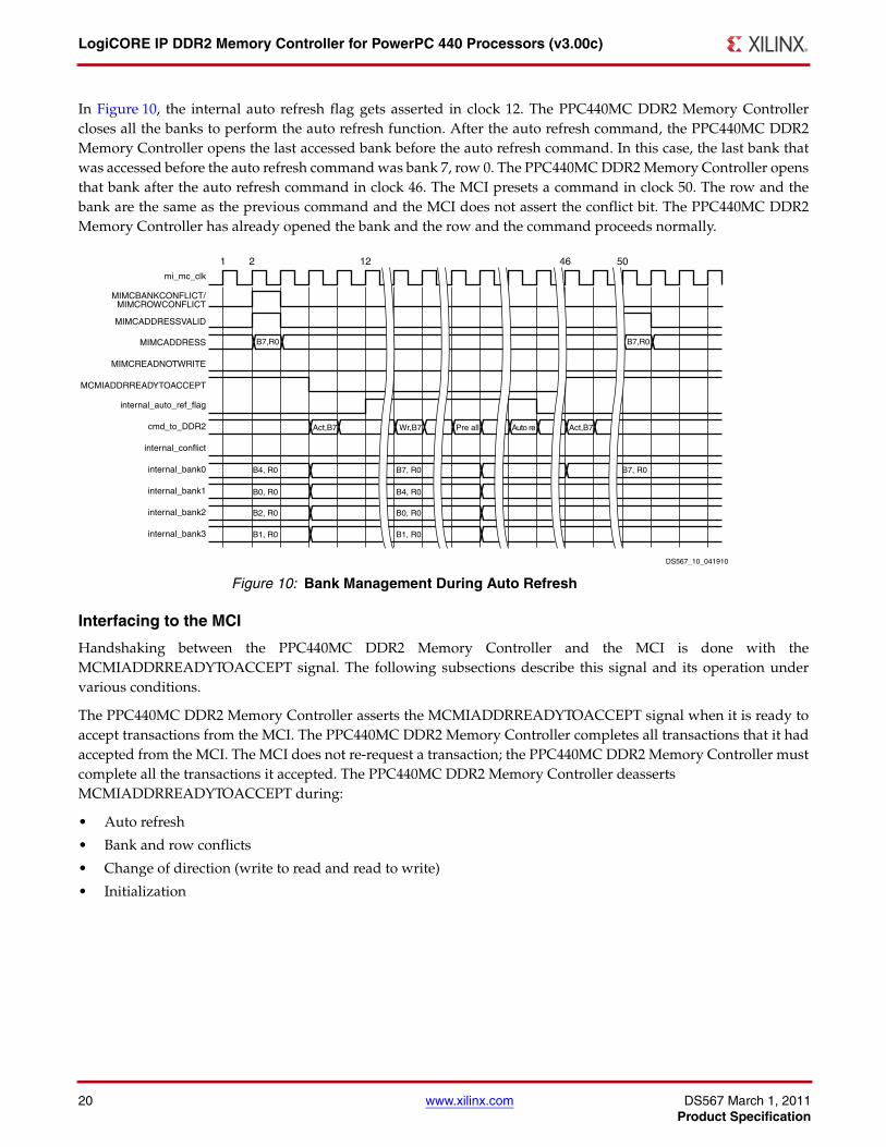
In Figure 10, the internal auto refresh flag gets asserted in clock 12. The PPC440MC DDR2 Memory Controllercloses all the banks to perform the auto refresh function. After the auto refresh command, the PPC440MC DDR2Memory Controller opens the last accessed bank before the auto refresh command. In this case, the last bank thatwas accessed before the auto refresh command was bank 7, row 0. The PPC440MC DDR2 Memory Controller opensthat bank after the auto refresh command in clock 46. The MCI presets a command in clock 50. The row and thebank are the same as the previous command and the MCI does not assert the conflict bit. The PPC440MC DDR2Memory Controller has already opened the bank and the row and the command proceeds normally.
Interfacing to the MCI
Handshaking between the PPC440MC DDR2 Memory Controller and the MCI is done with theMCMIADDRREADYTOACCEPT signal. The following subsections describe this signal and its operation undervarious conditions.
The PPC440MC DDR2 Memory Controller asserts the MCMIADDRREADYTOACCEPT signal when it is ready toaccept transactions from the MCI. The PPC440MC DDR2 Memory Controller completes all transactions that it hadaccepted from the MCI. The MCI does not re-request a transaction; the PPC440MC DDR2 Memory Controller mustcomplete all the transactions it accepted. The PPC440MC DDR2 Memory Controller deassertsMCMIADDRREADYTOACCEPT during:
• Auto refresh
• Bank and row conflicts
• Change of direction (write to read and read to write)
• Initialization
X-Ref Target - Figure 10
Figure 10: Bank Management During Auto Refresh
1 2
B7,R0
mi_mc_clk
internal_auto_ref_flag
internal_conflict
internal_bank0
internal_bank1
internal_bank2
internal_bank3
cmd_to_DDR2
B7,R0
DS567_10_041910
Act,B7 Wr,B7 Pre all Act,B7
B7, R0B7, R0
B4, R0
B0, R0
B1, R0
B4, R0
B0, R0
B2, R0
B1, R0
Auto re
12 46 50
MIMCBANKCONFLICT/MIMCROWCONFLICT
MIMCADDRESSVALID
MIMCADDRESS
MCMIADDRREADYTOACCEPT
MIMCREADNOTWRITE

DS567 March 1, 2011 www.xilinx.com 21Product Specification
LogiCORE IP DDR2 Memory Controller for PowerPC 440 Processors (v3.00c)
Auto Refresh
The PPC440MC DDR2 Memory Controller deasserts the MCMIADDRREADYTOACCEPT signal once the autorefresh flag is asserted internally. The auto refresh flag is asserted by the PPC440MC DDR2 Memory Controllerwhen it has to perform an auto refresh function to the DDR2 memory. Due to the synchronization delay, the MCIsees the deassertion of this signal after a delay of two clock cycles. The MCI can request transactions when thePPC440MC DDR2 Memory Controller deasserts the MCMIADDRREADYTOACCEPT signal because of thesynchronization delay. The PPC440MC DDR2 Memory Controller asserts and deasserts this signal two cyclesearlier to account for the synchronization delay.
The minimum DDR2 burst size is four. When the PPC440MC DDR2 Memory Controller is set to a burst of 4x64, theMCI must be set to a burst of 2x128. When set to the DDR2 burst size of four, the MCI can request transactions everyother clock, which can cause the MCI to request at least one transaction while MCMIADDRREADYTOACCEPT isdeasserted. The PPC440MC DDR2 Memory Controller accepts requests from the MCI for up to two clocks after thedeassertion of the MCMIADDRREADYTOACCEPT signal. The transaction that was accepted by the PPC440MCDDR2 Memory Controller after the deassertion of the MCMIADDRREADYTOACCEPT signal is processed after theauto refresh command completes.
In Figure 11 through Figure 14, the DDR2 burst size is 4.
In Figure 11, the PPC440MC DDR2 Memory Controller deasserts the MCMIADDRREADYTOACCEPT signal inclock 6 in response to the assertion of the internal auto refresh flag in clock 5. The MCI presents two commands inclock 3 and clock 5, while the MCMIADDRREADYTOACCEPT signal is asserted. The PPC440MC DDR2 MemoryController processes both commands before the auto refresh command to the memory. The PPC440MC DDR2Memory Controller asserts the MCMIADDRREADYTOACCEPT signal in clock 15 after the auto refresh commandcompletes.
In Figure 12, the MCI presents a command in clock 7 after the deassertion of the MCMIADDRREADYTOACCEPTsignal. The PPC440MC DDR2 Memory Controller processes this command after the auto refresh commandcompletes. The assertion of the MCMIADDRREADYTOACCEPT signal is delayed until the second write commandcompletes. This can be done because the MCI sees the assertion of the MCMIADDRREADYTOACCEPT signal latedue to the synchronization delay and has a minimum delay of two PPC440MC DDR2 Memory Controller clocksbefore presenting a transaction.
X-Ref Target - Figure 11
Figure 11: Write Command During Auto Refresh and MCMIADDRREADYTOACCEPT Asserted
1 2 3 4 5 6 7 8 9 10 11 12 13 14 15 16 17 18
A0
mi_mc_clk
MIMCBANKCONFLICT/MIMCROWCONFLICT
MIMCADDRESSVALID
MIMCADDRESS
MCMIADDRREADYTOACCEPT
MIMCREADNOTWRITE
internal_auto_ref_flag
cmd_to_DDR2
DDR2_data_bus
A1
DS567_11_041910
Wr,A0
auto_ref
A0,D0A0,D1
A0,D2A0,D3
A1,D0A1,D1
A1,D2A1,D3
Wr,A1
LogiCORE IP DDR2 Memory Controller for PowerPC 440 Processors (v3.00c)
22 www.xilinx.com DS567 March 1, 2011Product Specification
Bank and Row Conflicts
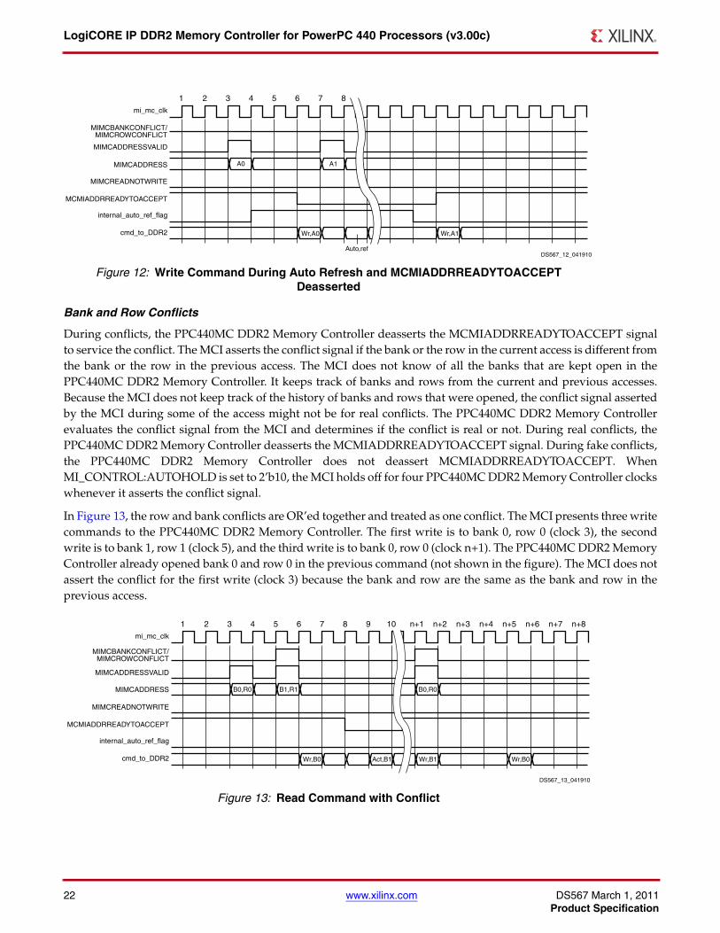
During conflicts, the PPC440MC DDR2 Memory Controller deasserts the MCMIADDRREADYTOACCEPT signalto service the conflict. The MCI asserts the conflict signal if the bank or the row in the current access is different fromthe bank or the row in the previous access. The MCI does not know of all the banks that are kept open in thePPC440MC DDR2 Memory Controller. It keeps track of banks and rows from the current and previous accesses.Because the MCI does not keep track of the history of banks and rows that were opened, the conflict signal assertedby the MCI during some of the access might not be for real conflicts. The PPC440MC DDR2 Memory Controllerevaluates the conflict signal from the MCI and determines if the conflict is real or not. During real conflicts, thePPC440MC DDR2 Memory Controller deasserts the MCMIADDRREADYTOACCEPT signal. During fake conflicts,the PPC440MC DDR2 Memory Controller does not deassert MCMIADDRREADYTOACCEPT. WhenMI_CONTROL:AUTOHOLD is set to 2’b10, the MCI holds off for four PPC440MC DDR2 Memory Controller clockswhenever it asserts the conflict signal.
In Figure 13, the row and bank conflicts are OR’ed together and treated as one conflict. The MCI presents three writecommands to the PPC440MC DDR2 Memory Controller. The first write is to bank 0, row 0 (clock 3), the secondwrite is to bank 1, row 1 (clock 5), and the third write is to bank 0, row 0 (clock n+1). The PPC440MC DDR2 MemoryController already opened bank 0 and row 0 in the previous command (not shown in the figure). The MCI does notassert the conflict for the first write (clock 3) because the bank and row are the same as the bank and row in theprevious access.
X-Ref Target - Figure 12
Figure 12: Write Command During Auto Refresh and MCMIADDRREADYTOACCEPT Deasserted
X-Ref Target - Figure 13
Figure 13: Read Command with Conflict
1 2 3 4 5 6 7 8
A0
mi_mc_clk
internal_auto_ref_flag
cmd_to_DDR2
A1
DS567_12_041910
Wr,A0
Auto,ref
Wr,A1
MIMCBANKCONFLICT/MIMCROWCONFLICT
MIMCADDRESSVALID
MIMCADDRESS
MCMIADDRREADYTOACCEPT
MIMCREADNOTWRITE
1 2 3 4 5 6 7 8 9 10 n+1 n+2 n+3 n+4 n+5 n+6 n+7 n+8
B0,R0
mi_mc_clk
internal_auto_ref_flag
cmd_to_DDR2
B1,R1
DS567_13_041910
Wr,B0 Act,B1
B0,R0
Wr,B1 Wr,B0
MIMCBANKCONFLICT/MIMCROWCONFLICT
MIMCADDRESSVALID
MIMCADDRESS
MCMIADDRREADYTOACCEPT
MIMCREADNOTWRITE
DS567 March 1, 2011 www.xilinx.com 23Product Specification
LogiCORE IP DDR2 Memory Controller for PowerPC 440 Processors (v3.00c)
The MCI asserts the conflict bit while presenting the second write (clock 5). The conflict bit is asserted because therow and bank are different from the row and bank in write 1 (clock 3). The PPC440MC DDR2 Memory Controllerhad not opened bank 1, row 1 during any of its previous accesses. The PPC440MC DDR2 Memory Controllerevaluates this conflict as a real conflict and deasserts the MCMIADDRREADYTOACCEPT signal in two or moreclock cycles. The PPC440MC DDR2 Memory Controller opens bank 1, row 1 and issues the write command. ThePPC440MC DDR2 Memory Controller asserts the MCMIADDRREADYTOACCEPT signal when it is ready toaccept new requests.
When presenting the third write in clock n+1, the MCI asserts the conflict bit. It asserts the conflict bit because thebank and row in the third write (clock n+1) is different from the bank and row in the second write (clock 7). ThePPC440MC DDR2 Memory Controller does not treat the third write (clock n+1) as a conflict because the bank androw for the third write were opened during the first write and have not been closed. The PPC440MC DDR2 MemoryController evaluates this conflict as a fake conflict and does not deassert the MCMIADDRREADYTOACCEPTsignal. The PPC440MC DDR2 Memory Controller takes at least two clock cycles to evaluate the conflict, and thereare at least four idle cycles in the DDR2_data_bus.
Change of Direction
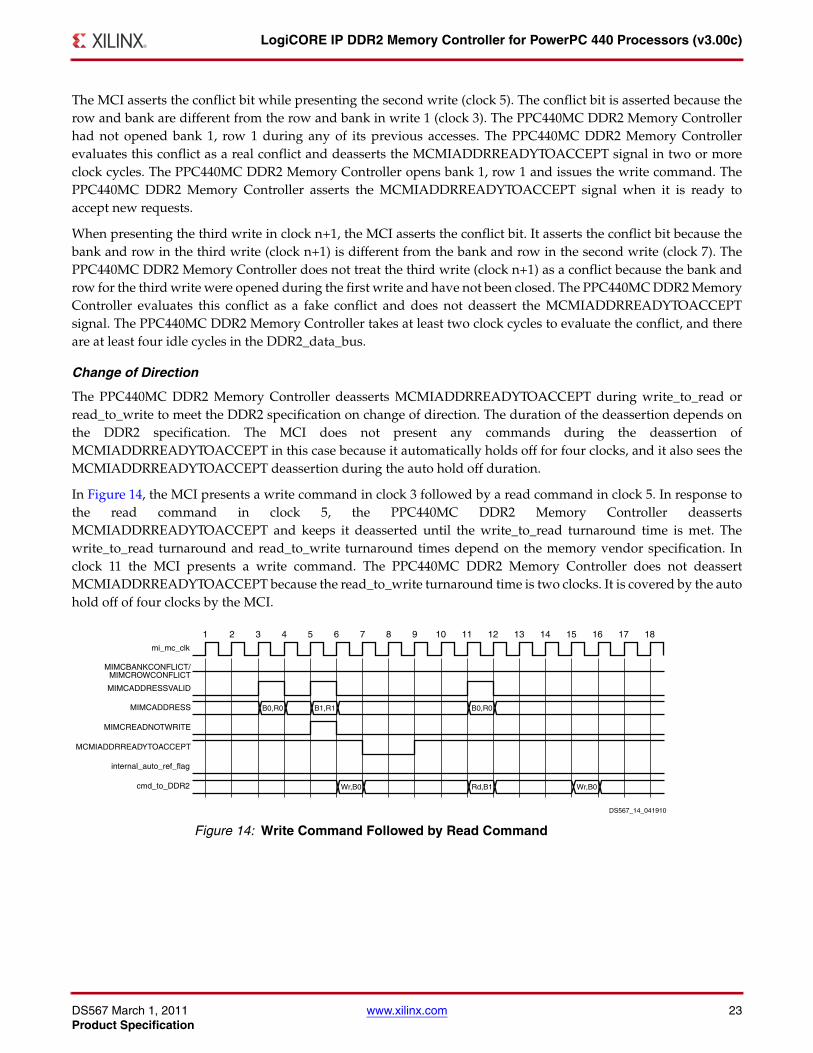
The PPC440MC DDR2 Memory Controller deasserts MCMIADDRREADYTOACCEPT during write_to_read orread_to_write to meet the DDR2 specification on change of direction. The duration of the deassertion depends onthe DDR2 specification. The MCI does not present any commands during the deassertion ofMCMIADDRREADYTOACCEPT in this case because it automatically holds off for four clocks, and it also sees theMCMIADDRREADYTOACCEPT deassertion during the auto hold off duration.
In Figure 14, the MCI presents a write command in clock 3 followed by a read command in clock 5. In response tothe read command in clock 5, the PPC440MC DDR2 Memory Controller deassertsMCMIADDRREADYTOACCEPT and keeps it deasserted until the write_to_read turnaround time is met. Thewrite_to_read turnaround and read_to_write turnaround times depend on the memory vendor specification. Inclock 11 the MCI presents a write command. The PPC440MC DDR2 Memory Controller does not deassertMCMIADDRREADYTOACCEPT because the read_to_write turnaround time is two clocks. It is covered by the autohold off of four clocks by the MCI.X-Ref Target - Figure 14
Figure 14: Write Command Followed by Read Command
1 2 3 4 5 6 7 8 9 10 11 12 13 14 15 16 17 18
B0,R0
mi_mc_clk
internal_auto_ref_flag
cmd_to_DDR2
B1,R1
DS567_14_041910
Wr,B0 Rd,B1 Wr,B0
B0,R0
MIMCBANKCONFLICT/MIMCROWCONFLICT
MIMCADDRESSVALID
MIMCADDRESS
MCMIADDRREADYTOACCEPT
MIMCREADNOTWRITE

LogiCORE IP DDR2 Memory Controller for PowerPC 440 Processors (v3.00c)
24 www.xilinx.com DS567 March 1, 2011Product Specification
Initialization
The MCMIADDRREADYTOACCEPT signal is deasserted during the entire duration of initialization andcalibration. At the end of the initialization and calibration sequence, the PPC440MC DDR2 Memory Controllerasserts the MCMIADDRREADYTOACCEPT signal. The calibration sequence is done once during initialization andis not repeated.
ECC FeatureThe built in Hamming code error correction feature in the Virtex-5 FXT FPGA block RAM using the FIFO36_72primitive supports the ECC feature in this memory controller. With this feature, double bit errors can be detectedand a single bit error can be corrected. The MCMIREADDATAERR signal provides the double bit error status andshould only be considered when the C_INCLUDE_ECC_SUPPORT parameter is asserted. Single bit error status canbe obtained from the rd_ecc_err[1] signal in the mem_if_top.v module. The rd_ecc_err[1] signal is not provided tothe MCI interface. The ECC feature is only supported with 128-bit MCI data width and 72-bit external memoryinterface width.
Bit 16 of the PPC440 MI_CONTROL register or the C_PPC440MC_CONTROL MHS parameter must be set to ‘1'when the ECC feature in the memory controller is enabled with the C_INCLUDE_ECC_SUPPORT parameter.
Read Modify Write
The computed ECC value for a write with partial byte enables will be incorrect because the disabled bytes stored inthe external memory location being accessed are not available during ECC calculation. Therefore, in case of writeswith partial byte enables the controller must issue an additional read to re-compute the ECC and write it back to theexternal memory device. When the memory controller detects a write with partial byte enables, theMCMIADDRREADYTOACCEPT signal is deasserted to prevent the MCI from issuing any more read or writecommand requests. The MCMIADDRREADYTOACCEPT signal remains deasserted until the additional readcommand (RMW_READ) followed by a write (RMW_WRITE) command have been executed by the memorycontroller. The data read back by the RMW_READ command is modified with data to be written for enabled bytesand stored in block RAM FIFOs (FIFO36_72) with the ECC feature turned ON. The RMW_WRITE command simplyreads the data to be written out of these FIFOs with the correct ECC value. At the end of the RMW_WRITEtransaction the MCMIADDRREADYTOACCEPT signal is asserted.
The target technology is an FPGA listed in the Supported Device Family field of the LogiCORE IP Facts table.
DS567 March 1, 2011 www.xilinx.com 25Product Specification
LogiCORE IP DDR2 Memory Controller for PowerPC 440 Processors (v3.00c)
Device Utilization and Performance Benchmarks
The HDL implementation modules automatically instantiate the necessary FPGA OBUF and IOBUF resources forthe DDR I/O signals.
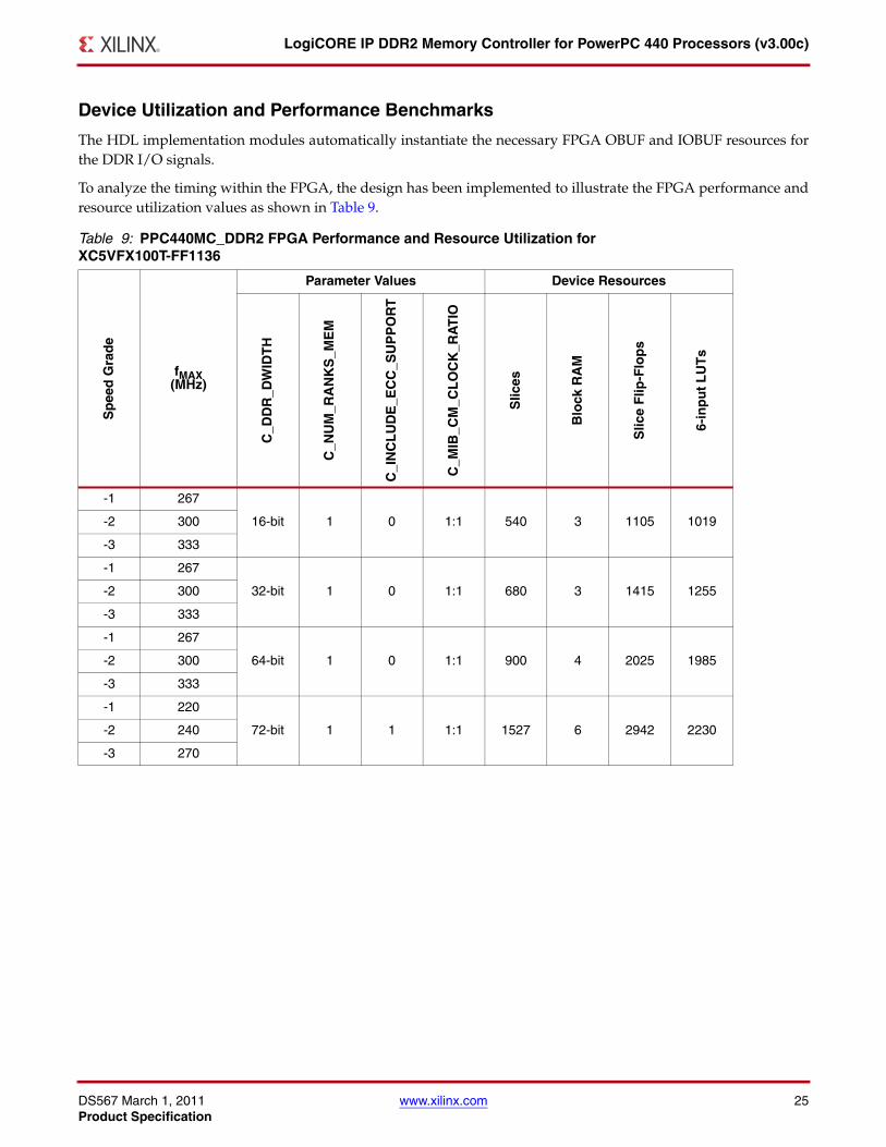
To analyze the timing within the FPGA, the design has been implemented to illustrate the FPGA performance andresource utilization values as shown in Table 9.
Table 9: PPC440MC_DDR2 FPGA Performance and Resource Utilization for XC5VFX100T-FF1136
Sp
eed
Gra
de
fMAX(MHz)
Parameter Values Device ResourcesC
_DD
R_D
WID
TH
C_N
UM
_RA
NK
S_M
EM
C_I
NC
LU
DE
_EC
C_S
UP
PO
RT
C_M
IB_C
M_C
LO
CK
_RA
TIO
Slic
es
Blo
ck R
AM
Slic
e F
lip-F
lop
s
6-in
pu
t L
UT
s
-1 267
16-bit 1 0 1:1 540 3 1105 1019-2 300
-3 333
-1 267
32-bit 1 0 1:1 680 3 1415 1255-2 300
-3 333
-1 267
64-bit 1 0 1:1 900 4 2025 1985-2 300
-3 333
-1 220
72-bit 1 1 1:1 1527 6 2942 2230-2 240
-3 270

LogiCORE IP DDR2 Memory Controller for PowerPC 440 Processors (v3.00c)
26 www.xilinx.com DS567 March 1, 2011Product Specification
Revision HistoryThe following table shows the revision history for this document.
Notice of DisclaimerXilinx is providing this product documentation, hereinafter "Information," to you "AS IS" with no warranty of any kind, expressor implied. Xilinx makes no representation that the Information, or any particular implementation thereof, is free from anyclaims of infringement. You are responsible for obtaining any rights you may require for any implementation based on theInformation. All specifications are subject to change without notice. XILINX EXPRESSLY DISCLAIMS ANY WARRANTYWHATSOEVER WITH RESPECT TO THE ADEQUACY OF THE INFORMATION OR ANY IMPLEMENTATION BASEDTHEREON, INCLUDING BUT NOT LIMITED TO ANY WARRANTIES OR REPRESENTATIONS THAT THISIMPLEMENTATION IS FREE FROM CLAIMS OF INFRINGEMENT AND ANY IMPLIED WARRANTIES OFMERCHANTABILITY OR FITNESS FOR A PARTICULAR PURPOSE. Except as stated herein, none of the Information may becopied, reproduced, distributed, republished, downloaded, displayed, posted, or transmitted in any form or by any meansincluding, but not limited to, electronic, mechanical, photocopying, recording, or otherwise, without the prior written consent ofXilinx.
Date Version Revision
01/15/08 1.0 Initial Xilinx release with ISE® 10.1 EDK software release.
03/19/08 1.1 Release with ISE 10.1 SP1 EDK software release.
03/31/08 1.1.1 Minor publication issue.
05/09/08 1.2
Revised version of reference design to v2_00_a. In Table 2, removed C_MIBDATA_WIDTH and added default values in C_MEM_BASEADDR, C_MEM_HIGHADDR, C_REG_DIMM, C_DQS_BITS, C_DQ_BITS, and C_NUM_IDELAYCTRL. Changed frequency for 72-bit C_DDR_DWIDTH in Table 9.
8/13/08 1.3 Incorporated CRs 477715 and 477717 to correct signal names and descriptions in Table 1.
10/15/08 1.4 Incorporated CR 479100; corrected Variable values in Table 8.
01/09/09 1.5 Incorporated edits to fix CRs 491863, 491981, 493334, 495692, and 496213.
04/24/09 1.6 Replaced references to supported device families and tool name(s) with hyperlinks to PDF files; Updated trademark information.
9/16/09 1.7 Updated for EDK_L 11.3 release; created v2.00c; added Memory Part Parameter Considerations section; updated images.
10/19/09 1.8 Updated for EDK_L 11.4 release; created v3.00a; added IDELAYCTRL Shared Pinout Considerations and Upgrading From PPC440MC_DDR2 v2.00.x to v3 sections.
4/19/10 1.9 Updated for 12.1 release.
3/11/11 2.0 Created v3.00c; incorporated CR566505; updated for the 13.1 release.