17 unit-i introduction to vlsi technology
TRANSCRIPT

1
https://nptel.ac.in/courses/117103066/17
UNIT-I
Introduction to VLSI Technology
Introduction:
The invention of the transistor by William B. Shockley, Walter H. Brattain and John Bardeen of
Bell Telephone Laboratories drastically changed the electronics industry and paved the way for
the development of the Integrated Circuit (IC) technology. The first IC was designed by Jack
Kilby at Texas Instruments at the beginning of 1960 and since that time there have already been
four generations of ICs .Viz SSI (small scale integration), MSI (medium scale integration), LSI
(large scale integration), and VLSI (very large scale integration). Now we are ready to see the
emergence of the fifth generation, ULSI (ultra large scale integration) which is characterized by
complexities in excess of 3 million devices on a single IC chip. Further miniaturization is still to
come and more revolutionary advances in the application of this technology must inevitably
occur.
Over the past several years, Silicon CMOS technology has become the dominant fabrication
process for relatively high performance and cost effective VLSI circuits. The revolutionary
nature of this development is understood by the rapid growth in which the number of transistors
integrated in circuits on a single chip.
METAL-OXIDE-SEMICONDUCTOR (MOS) AND RELATED VLSI TECHNOLOGY:
The MOS technology is considered as one of the very important and promising technologies in
the VLSI design process. The circuit designs are realized based on PMOS, NMOS, CMOS and
BiCMOS devices.
The PMOS devices are based on the p-channel MOS transistors. Specifically, the PMOS channel
is part of a n-type substrate lying between two heavily doped p+ wells beneath the source and
drain electrodes. Generally speaking, a PMOS transistor is only constructed in consort with an
NMOS transistor.

2
The NMOS technology and design processes provide an excellent background for other
technologies. In particular, some familiarity with NMOS allows a relatively easy transition to
CMOS technology and design.
The techniques employed in NMOS technology for logic design are similar to GaAs technology..
Therefore, understanding the basics of NMOS design will help in the layout of GaAs circuits
In addition to VLSI technology, the VLSI design processes also provides a new degree of
freedom for designers which helps for the significant developments. With the rapid advances in
technology the size of the ICs is shrinking and the integration density is increasing.
The minimum line width of commercial products over the years is shown in the graph below.
The graph shows a significant decrease in the size of the chip in recent years which implicitly
indicates the advancements in the VLSI technology.
BASIC MOS TRANSISTORS:
The MOS Transistor means, Metal-Oxide-Semiconductor Field Effect Transistor which is the
most basic element in the design of a large scale integrated circuits(IC).

3
These transistors are formed as a ``sandwich'' consisting of a semiconductor layer, usually a
slice, or wafer, from a single crystal of silicon; a layer of silicon dioxide (the oxide) and a layer
of metal. These layers are patterned in a manner which permits transistors to be formed in the
semiconductor material (the ``substrate''); a diagram showing a MOSFET is shown below in
Figure .
Silicon dioxide is a very good insulator, so a very thin layer, typically only a few hundred
molecules thick, is used. In fact , the transistors which are used do not use metal for their gate
regions, but instead use polycrystalline silicon (poly). Polysilicon gate FET's have replaced
virtually all of the older devices using metal gates in large scale integrated circuits. (Both metal
and polysilicon FET's are sometimes referred to as IGFET's (insulated gate field effect
transistors), since the silicon dioxide under the gate is an insulator.
MOS Transistors are classified as n-MOS, p-MOS and c-MOS Transistors based on the
fabrication .
NMOS devices are formed in a p-type substrate of moderate doping level. The source and drain
regions are formed by diffusing n- type impurities through suitable masks into these areas to give
the desired n-impurity concentration and give rise to depletion regions which extend mainly in
the more lightly doped p-region . Thus, source and drain are isolated from one another by two
diodes. Connections to the source and drain are made by a deposited metal layer. In order to
make a useful device, there must be the capability for establishing and controlling a current
between source and drain, and .this is commonly achieved in one of two ways, giving rise to the
enhancement mode and depletion mode transistors.
4
Enhancement Mode Transistors:
In an enhancement mode device a polysilicon gate is deposited on a layer of insulation over the
region between source and drain. In the diagram below channel is not established and the device
is in a non-conducting condition, i.e VD = Vs = Vgs = 0. If this gate is connected to a suitable
positive voltage with respect to the source, then the electric field established between the gate
and the substrate gives rise to a charge inversion region in the substrate under the gate insulation
and a conducting path or channel is formed between source and drain.
ENHANCEMENT MODE TRANSISTOR ACTION :
To understand the enhancement mechanism, let us consider the enhancement mode device. In
order to establish the channel, a minimum voltage level called threshold voltage (Vt) must be
established between gate and source. Fig. (a) Shows the existing situation where a channel is
established but no current flowing between source and drain (Vds = 0 ).
Let us now consider the conditions when current flows in the channel by applying a voltage Vds
between drain and source. The IR drop = Vds along the channel. This develops a voltage
between gate and channel varying with distance along the channel with the voltage being a
maximum of Vgs at the source end. Since the effective gate voltage is Vg= Vgs - Vt, (no current
flows when Vgs < Vt) there will be voltage available to invert the channel at the drain end so
long as Vgs - Vt ~ Vds· The limiting condition comes when Vds= Vgs - Vt. For all voltages Vds
< Vgs - Vt, the device is in the non-saturated region of operation which is the condition shown in
Fig. (b) below.

5

6
Let us now consider the situation when Vds is increased to a level greater than Vgs - Vt. In this
case, an IR drop equal to Vgs – Vt occurs over less than the whole length of the channel such
that, near the drain, there is insufficient electric field available to give rise to an inversion layer
to create the channel. The .channel is, therefore, 'pinched off as shown in Fig. (c). Diffusion
current completes the path from source to drain in this case, causing the channel to exhibit a high
resistance and behave as a constant current source. This region, known as saturation, is
.characterized by almost constant current for increase of Vds above Vds = Vgs - Vt. In all cases,
the channel will cease to exist and no current will flow when Vgs < Vt. Typically, for
enhancement mode devices, Vt = 1 volt for VDD = 5 V or, in general terms, Vt = 0.2 VDD.
DEPLETION MODE TSANSISTOR ACTION
N-MOS Depletion mode mosfets are built with P-type silicon substrates, and P-channel versions
are built on N-type substrates. In both cases they include a thin gate oxide formed between the
source and drain regions. A conductive channel is deliberately formed below the gate oxide layer
and between the source and drain by using ion-implantation. By implanting the correct ion
polarity in the channel region during fabrication determines the polarity of the threshold voltage
(i.e. -Vt for an N channel transistor, or +Vt for an P-channel transistor). The actual concentration
of ions in the substrate-to-channel region is used to adjust the threshold voltage (Vt) to the
desired value. Depletion-mode devices are a little more difficult to manufacture and their
characteristics harder to control than enhancement types, which do not require ion implantation.
In depletion mode devices the channel is established, due to the implant, even when Vgs = 0,
and to cause the channel to cease a negative voltage Vtd must be applied between gate and
source.

7
Vtd is typically < - 0.8 VDD, depending on the implant and substrate bias, but, threshold voltage
differences apart, the action is similar to that of the enhancement mode transistor.
CMOS FABRICATION :
CMOS fabrication is performed based on various methods , including the p-well, the n-well, the
twin-tub, and the silicon-on-insulator processes .Among these methods the p-well process is
widely used in practice and the n-well process is also popular, particularly as it is an easy
retrofit to existing NMOS lines.
(i) The p-well Process:
The p-well structure consists of an n-type substrate in which p-devices may be formed by
suitable masking and diffusion and, in order to accommodate n-type devices, a deep p-well is
diffused into the n-type substrate as shown in the Fig.below.
This diffusion should be carried out with special care since the p-well doping concentration and
depth will affect the threshold voltages as well as the breakdown voltages of the n-transistors. To
achieve low threshold voltages (0.6 to 1.0 V) either deep-well diffusion or high-well resistivity is
required. However, deep wells require larger spacing between the n- and p-type transistors and
wires due to lateral diffusion and therefore a larger chip area. The p-wells Act as substrates for
the n-devices within the parent n-substrate, and, the two areas are electrically isolated.
Except this in all other respects- like masking, patterning, and diffusion-the process is similar to
NMOS fabrication.

8
P-well fabrication process(Figs 1,2,3 & 4)
The diagram below shows the CMOS p-well inverter showing VDD and Vss substrate
connections

9
The n-well Process : Though the p-well process is widely used in C-MOS fabrication the n-well
fabrication is also very popular because of the lower substrate bias effects on transistor threshold
voltage and also lower parasitic capacitances associated with source and drain regions.
The typical n-well fabrication steps are shown in the diagram below.
Fig. n-well fabrication steps
The first mask defines the n-well regions. This is followed by a low dose phosphorus implant
driven in by a high temperature diffusion step to form the n-wells. The well depth is optimized to
ensure against-substrate top+ diffusion breakdown without compromising then-well to n+ mask
separation. The next steps are to define the devices and diffusion paths, grow field oxide, deposit
and pattern the poly silicon, carry out the diffusions, make contact cuts, and finally metalize as
before. Lt will be seen that an n+ mask and its complement may be used to define the n- and p-
diffusion regions respectively. These same masks also include the VDD and Vss contacts
(respectively). It should be noted that, alternatively, we could have used a p+ mask and its
complement since the n + and p + masks are generally complementary.
The diagram below shows the Cross-sectional view of n-well CMOS Inverter.

10
Due to the differences in charge carrier mobilities, the n-well process creates non-optimum p-
channel characteristics. However, in many CMOS designs (such as domino-logic and dynamic
logic structures), this is relatively unimportant since they contain a preponderance of n-channel
devices. Thus then-channel transistors are mainly those used to form1ogic elements, providing
speed and high density of elements.
However, a factor of the n-well process is that the performance of the already poorly performing
p-transistor is even further degraded. Modern process lines have come to grips with these
problems, and good device performance may be achieved for both p-well and n-well fabrication.
BICMOS Technology:
A Bi-CMOS circuit of both bipolar junction transistors and MOS transistors on a single
substrate. The driving capability of MOS transistors is less because of limited current sourcing
and sinking capabilities of the transistors. To drive large capacitive loads Bi-CMOS technology
is used. As this technology combines Bipolar and CMOS transistors in a single integrated circuit,
it has the advantages of both bipolar and CMOS transistors. Bi-CMOS is able to achieve VLSI
circuits with speed-power-density performance previously not possible with either technology
individually. The diagram given below shows the cross section of the Bi-CMOS process which
uses an NPN transistor

11
Fig. Arrangement of Bi-CMOS npn transistor
The lay-out view of Bic-MOS transistor is shown in the figure below. The fabrication of Bi-
CMOS is similar to CMOS but with certain additional process steps and additional masks are
considered. They are (i) the p+ base region; (ii) n+ collector area; and (iii) the buried sub
collector (BCCD).
IDS-VDS characteristics of MOS Transistor:
The graph below shows the ID Vs VDS characteristics of an n- MOS transistor for several values
of VGS .It is clear that there are two conduction states when the device is ON. The saturated state
and the non-saturated state. The saturated curve is the flat portion and defines the saturation
region. For Vgs < VDS + Vth, the NMOS device is conducting and ID is independent of VDS. For
Vgs > VDS + Vth, the transistor is in the non-saturation region and the curve is a half parabola.
When the transistor is OFF (Vgs < Vth), then ID is zero for any VDS value.

12
The boundary of the saturation/non-saturation bias states is a point seen for each curve in the
graph as the intersection of the straight line of the saturated region with the quadratic curve of
the non-saturated region. This intersection point occurs at the channel pinch off voltage called
VDSAT. The diamond symbol marks the pinch-off voltage VDSAT for each value of VGS. VDSAT is
defined as the minimum drain-source voltage that is required to keep the transistor in saturation
for a given VGS .In the non-saturated state, the drain current initially increases almost linearly
from the origin before bending in a parabolic response. Thus the name ohmic or linear for the
non- saturated region.
The drain current in saturation is virtually independent of VDS and the transistor acts as a current
Source. This is because there is no carrier inversion at the drain region of the channel. Carriers
are pulled into the high electric field of the drain/substrate pn junction and ejected out of the
drain terminal.

13
Drain-to-Source Current IDS versus Voltage VDS Relationships:
The working of a MOS transistor is based on the principle that the use of a voltage on the gate
induce a charge in the channel between source and drain, which may then be caused to move
from source to drain under the influence of an electric field created by voltage Vds applied
between drain and source. Since the charge induced is dependent on the gate to source voltage
Vgs then Ids is dependent on both Vgs and Vds.
Let us consider the diagram below in which electrons will flow source to drain .So, the drain
current is given by
Charge induced in channel (Qc)
Ids =-Isd = _____________________
Electron transit time(τ)
Length of the channel
Where the transit time is given by τsd = ------------------------------
Velocity (v)

14
But velocity v= µeds
Where µ =electron or hole mobility and Eds = Electric field
Also , Eds = Vds/L
So, v = µ.Vds/L
And τds = L2 / µ.Vds
The typical values of µ at room temperature are given below.
The Non-saturated Region:
Let us consider the Id vs Vd relationships in the non-saturated region .The charge induced in the
channel due to due to the voltage difference between the gate and the channel, Vgs (assuming
substrate connected to source). The voltage along the channel varies linearly with distance X
from the source due to the IR drop in the channel .In the non-saturated state the average value is
Vds/2. Also the effective gate voltage Vg = Vgs – Vt where Vt, is the threshold voltage needed
to invert the charge under the gate and establish the channel.
Hence the induced charge is Qc = Eg εins εow. L

15
Where
Eg = average electric field gate to channel
Εins = relative permittivity of insulation between gate and channel
Εo = permittivity of free space.
So, we can write that
Here D is the thickness of the oxide layer. Thus
So, by combining the above two equations ,we get
Or the above equation can be written as
In the non-saturated or resistive region where Vds < Vgs – Vt and
Generally ,a constant β is defined as
So that ,the expression for drain –source current will become
The gate /channel capacitance is
16
Hence we can write another alternative form forthe drain current as
Some time it is also convenient to use gate –capacitance per unit area ,Cg
So,the drain current is
This is the relation between drain current and drain-source voltage in non-saturated region.
The Saturated Region
Saturation begins when Vds = Vgs - V, since at this point the IR drop in the channel equals the
effective gate to channel voltage at the drain and we may assume that the current remains fairly
constant as Vds increases further. Thus
Or we can also write that
Or it can also be written as
Or
The expressions derived above for Ids hold for both enhancement and depletion mode devices.
Here the threshold voltage for the NMOS depletion mode device (denoted as Vtd) is negative.

17
MOS Transistor Threshold Voltage Vt :
The gate structure of a MOS transistor consists, of charges stored in the dielectric layers and in
the surface to surface interfaces as well as in the substrate itself. Switching an enhancement
mode MOS transistor from the off to the on state consists in applying sufficient gate voltage to
neutralize these charges and enable the underlying silicon to undergo an inversion due to the
electric field from the gate. Switching a depletion mode NMOS transistor from the on to the off
state consists in applying enough voltage to the gate to add to the stored charge and invert the 'n'
implant region to 'p'.
The threshold voltage Vt may be expressed as:
Where QD = the charge per unit area in the depletion layer below the oxide
Qss = charge density at Si: sio2 interface
Co =Capacitance per unit area.
Φns = work function difference between gate and Si
Φfn = Fermi level potential between inverted surface and bulk Si
For polynomial gate and silicon substrate, the value of Φns is negative but negligible and the
magnitude and sign of Vt are thus determined by balancing the other terms in the equation.
To evaluate the Vt the other terms are determined as below.
Body Effect :
Generally while studying the MOS transistors it is treated as a three terminal device. But ,the
body of the transistor is also an implicit terminal which helps to understand the characteristICs of
the transistor. Considering the body of the MOS transistor as a terminal is known as the body

18
effect. The potential difference between the source and the body (Vsb) affects the threshold
voltage of the transistor. In many situations, this Body Effect is relatively insignificant, so we
can (unless otherwise stated) ignore the Body Effect. But it is not always insignificant, in some
cases it can have a tremendous impact on MOSFET circuit performance.
Body effect - NMOS device
Increasing Vsb causes the channel to be depleted of charge carriers and thus the threshold
voltage is raised. Change in Vt is given by δvt = γ.(Vsb)1/2 where γ is a constant which depends
on substrate doping so that the more lightly doped the substrate, the smaller will be the body
effect
The threshold voltage can be written as
Where Vt(0) is the threshold voltage for Vsd = 0
For n-MOS depletion mode transistors ,the body voltage values at different VDD voltages are
given below.
VSB = 0 V ; Vsd = -0.7VDD (= - 3.5 V for VDD =+5V )
VSB = 5 V ; Vsd = -0.6VDD (= - 3.0 V for VDD =+5V )
The NMOS INVERTER :
An inverter circuit is a very important circuit for producing a complete range of logic circuits.
This is needed for restoring logic levels, for Nand and Nor gates, and for sequential and memory
circuits of various forms .

19
A simple inverter circuit can be constructed using a transistor with source connected to ground
and a load resistor of connected from the drain to the positive supply rail VDD· The output is
taken from the drain and the input applied between gate and ground .
But, during the fabrication resistors are not conveniently produced on the silicon substrate and
even small values of resistors occupy excessively large areas .Hence some other form of load
resistance is used. A more convenient way to solve this problem is to use a depletion mode
transistor as the load, as shown in Fig. Below.
The salient features of the n-MOS inverter are
• For the depletion mode transistor, the gate is connected to the source so it is always on .
• In this configuration the depletion mode device is called the pull-up (P.U) and the
enhancement mode device the pull-down (P.D) transistor.
• With no current drawn from the output, the currents Ids for both transistors must be
equal.
NMOS Inverter transfer characteristic.
The transfer characteristic is drawn by taking Vds on x-axis and Ids on Y-axis for both
enhancement and depletion mode transistors. So,to obtain the inverter transfer characteristic for
Vgs = 0 depletion mode characteristic curve is superimposed on the family of curves for the

20
enhancement mode device and from the graph it can be seen that , maximum voltage across the
enhancement mode device corresponds to minimum voltage across the depletion mode transistor.
From the graph it is clear that as Vin(=Vgs p.d. Transistor) exceeds the Pulldown threshold
voltage current begins to flow. The output voltage Vout thus decreases and the subsequent
increases in Vin will cause the Pull down transistor to come out of saturation and become
resistive.
CMOS Inverter :
The inverter is the very important part of all digital designs. Once its operation and properties
are clearly understood, Complex structures like NAND gates, adders, multipliers, and
microprocessors can also be easily done. The electrical behavior of these complex circuits can be
almost completely derived by extrapolating the results obtained for inverters. As shown in the
diagram below the CMOS transistor is designed using p-MOS and n-MOS transistors.

21
In the inverter circuit ,if the input is high .the lower n-MOS device closes to discharge the
capacitive load .Similarly ,if the input is low,the top p-MOS device is turned on to charge the
capacitive load .At no time both the devices are on ,which prevents the DC current flowing from
positive power supply to ground. Qualitatively this circuit acts like the switching circuit, since
the p-channel transistor has exactly the opposite characteristICs of the n-channel transistor. In the
transition region both transistors are saturated and the circuit operates with a large voltage gain.
The C-MOS transfer characteristic is shown in the below graph.
Considering the static conditions first, it may be Seen that in region 1 for which Vi,. = logic 0,
we have the p-transistor fully turned on while the n-transistor is fully turned off. Thus no current
flows through the inverter and the output is directly connected to VDD through the p-transistor.
Hence the output voltage is logic 1 . In region 5 , Vin = logic 1 and the n-transistor is fully on
while the p-transistor is fully off. So, no current flows and a logic 0 appears at the output.
In region 2 the input voltage has increased to a level which just exceeds the threshold voltage of
the n-transistor. The n-transistor conducts and has a large voltage between source and drain; so it
is in saturation. The p-transistor is also conducting but with only a small voltage across it, it
operates in the unsaturated resistive region. A small current now flows through the inverter from
VDD to VSS. If we wish to analyze the behavior in this region, we equate the p-device resistive
region current with the n-device saturation current and thus obtain the voltage and current
relationships.

22
Region 4 is similar to region 2 but with the roles of the p- and n-transistors reversed.However,
the current magnitudes in regions 2 and 4 are small and most of the energy consumed in
switching from one state to the other is due to the larger current which flows in region 3.
Region 3 is the region in which the inverter exhibits gain and in which both transistors are in
saturation.
The currents in each device must be the same ,since the transistors are in series. So,we can write
that
Since both transistors are in saturation, they act as current sources so that the equivalent circuit in
this region is two current sources in series between VDD and Vss with the output voltage coming
from their common point. The region is inherently unstable in consequence and the changeover
from one logic level to the other is rapid.
Determination of Pull-up to Pull –Down Ratio (Zp.uZp.d.)For an NMOS Inverter driven
by another NMOS Inverter :
Let us consider the arrangement shown in Fig.(a). In which an inverter is driven from the output
of another similar inverter. Consider the depletion mode transistor for which Vgs = 0 under all
conditions, and also assume that in order to cascade inverters without degradation the condition
Fig.(a).Inverter driven by another inverter.

23
For equal margins around the inverter threshold, we set Vinv = 0.5VDD · At this point both
transistors are in saturation and we can write that
Where Wp.d , Lp.d , Wp.u. And Lp.u are the widths and lengths of the pull-down and pull-up
transistors respectively.
So,we can write that

24
The typical, values for Vt ,Vinv and Vtd are
Substituting these values in the above equation ,we get
Here
So,we get
This is the ratio for pull-up to pull down ratio for an inverter directly driven by another inverter.
Pull -Up to Pull-Down ratio for an NMOS Inverter driven through one or more Pass
Transistors
Let us consider an arrangement in which the input to inverter 2 comes from the output of
inverter 1 but passes through one or more NMOS transistors as shown in Fig. Below (These
transistors are called pass transistors).

25
The connection of pass transistors in series will degrade the logic 1 level / into inverter 2 so that
the output will not be a proper logic 0 level. The critical condition is , when point A is at 0 volts
and B is thus at VDD. But the voltage into inverter 2at point C is now reduced from VDD by the
threshold voltage of the series pass transistor. With all pass transistor gates connected to VDD
there is a loss of Vtp, however many are connected in series, since no static current flows
through them and there can be no voltage drop in the channels. Therefore, the input voltage to
inverter 2 is
Vin2 = VDD- Vtp
Where Vtp = threshold voltage for a pass transistor.
Let us consider the inverter 1 shown in Fig.(a) with input = VDD· If the input is at VDD , then the
pull-down transistor T2 is conducting but with a low voltage across it; therefore, it is in its
resistive region represented by R1 in Fig.(a) below. Meanwhile, the pull up transistor T1 is in
saturation and is represented as a current source.
For the pull down transistor
Since Vds is small, Vds/2 can be neglected in the above expression.
26
So,
Now, for depletion mode pull-up transistor in saturation with Vgs = 0
The product I1R1 = Vout1
So,
Let us now consider the inverter 2 Fig.b .when input = VDD- Vtp.

27
Whence,
If inverter 2 is to have the same output voltage under these conditions then Vout1 = Vout2. That is
I1R1=I2R2 , therefore
Considering the typical values
Therefore
From the above theory it is clear that, for an n-MOS transistor
(i). An inverter driven directly from the output of another should have a Zp.u/ Zpd. Ratio
Of ≥ 4/1.
(ii).An inverter driven through one or more pass transistors should have a Zp.u./Zp.d ratio of ≥8/1

28
ALTERMTIVE FORMS OF PULL –UP
Generally the inverter circuit will have a depletion mode pull-up transistor as its load. But there
are also other configurations .Let us consider four such arrangements.
(i).Load resistance RL : This arrangement consists of a load resistor as apull-up as shown in the
diagram below.But it is not widely used because of the large space requirements of resistors
produced in a silicon substrate.
2. NMOS depletion mode transistor pull-up : This arrangement consists of a depletion mode
transistor as pull-up. The arrangement and the transfer characteristic are shown below.In this
type of arrangement we observe
(a) Dissipation is high , since rail to rail current flows when Vin = logical 1.
(b) Switching of output from 1 to 0 begins when Vin exceeds Vt, of pull-down device.

29
NMOS depletion mode transistor pull-up and transfer characteristic
(c) When switching the output from 1 to 0, the pull-up device is non-saturated initially and this
presents lower resistance through which to charge capacitive loads .
3. NMOS enhancement mode pull-up :This arrangement consists of a n-MOS enhancement
mode transistor as pull-up. The arrangement and the transfer characteristic are shown below.
NMOS enhancement mode pull-up and transfer characteristic
The important features of this arrangement are
(a) Dissipation is high since current flows when Vin =logical 1 (VGG is returned to VDD) .
(b) Vout can never reach VDD (logical I) if VGG = VDD as is normally the case.
(c) VGG may be derived from a switching source, for example, one phase of a clock, so that
Dissipation can be greatly reduced.
(d) If VGG is higher than VDD then an extra supply rail is required.
4. Complementary transistor pull-up (CMOS) : This arrangement consists of a C-MOS
arrangement as pull-up. The arrangement and the transfer characteristic are shown below

30
The salient features of this arrangement are
(a) No current flows either for logical 0 or for logical 1 inputs.
(b) Full logical 1 and 0 levels are presented at the output.
(c) For devices of similar dimensions the p-channel is slower than the n-channel device.
THE BiCMOS INVERTER :
A BiCMOS inverter, consists of a PMOS and NMOS transistor ( M2 and M1), two NPN
bipolar junction transistors,( Q2 and Q1), and two impedances which act as loads( Z2 and Z1) as
shown in the circuit below.

31
When input, Vin, is high (VDD), the NMOS transistor ( M1), turns on, causing Q1 to
conduct,while M2 and Q2 are off, as shown in figure (b) . Hence , a low (GND) voltage is
translated to the output Vout. On the other hand, when the input is low, the M2 and Q2 turns on,
while m1and Q1 turns off, resulting to a high output level at the output as shown in Fig.(b).
In steady-state operation, Q1 and Q2 never turns on or off simultaneously, resulting to a lower
power consumption. This leads to a push-pull bipolar output stage. Transistors m1and M2, on
the other hand, works as a phase-splitter, which results to a higher input impedance.
The impedances Z2 and Z1 are used to bias the base-emitter junction of the bipolar transistor and
to ensure that base charge is removed when the transistors turn off. For example when the input
voltage makes a high-to-low transition, M1 turns off first. To turn off Q1, the base charge must
be removed, which can be achieved by Z1.With this effect, transition time reduces. However,

32
there exists a short time when both Q1 and Q2 are on, making a direct path from the supply
(VDD) to the ground. This results to a current spike that is large and has a detrimental effect on
both the noise and power consumption, which makes the turning off of the bipolar transistor
fast .
Comparison of BiCMOS and C-MOS technologies
The BiCMOS gates perform in the same manner as the CMOS inverter in terms of power
consumption, because both gates display almost no static power consumption.
When comparing BiCMOS and CMOS in driving small capacitive loads, their performance are
comparable, however, making BiCMOS consume more power than CMOS. On the other hand,
driving larger capacitive loads makes BiCMOS in the advantage of consuming less power than
CMOS, because the construction of CMOS inverter chains are needed to drive large capacitance
loads, which is not needed in BiCMOS.
The BiCMOS inverter exhibits a substantial speed advantage over CMOS inverters, especially
when driving large capacitive loads. This is due to the bipolar transistor’s capability of
effectively multiplying its current.
For very low capacitive loads, the CMOS gate is faster than its BiCMOS counterpart due to
small values of Cint. This makes BiCMOS ineffective when it comes to the implementation of
internal gates for logic structures such as alus, where associated load capacitances are small.
BiCMOS devices have speed degradation in the low supply voltage region and also BiCMOS is
having greater manufacturing complexity than CMOS.

UNIT II
VLSI CIRCUIT DESIGN PROCESSES
In this chapter we will be studying how to get the schematic into stick diagrams or layouts.
MOS circuits are formed on four basic layers:
N-diffusion
P-diffusion
Poly silicon
Metal
These layers are isolated by one another by thick or thin silicon dioxide insulating
layers. Thin oxide mask region includes n-diffusion / p-diffusion and transistor channel.
Stick diagrams:
Stick diagrams may be used to convey layer information through the use of a color code.
For example:
N-diffusion -green
poly -- red
Blue -- metal
yellow --implant
Black --contact area

Encodings for NMOS process:
Figure shows the way of representing different layers in stick diagram notation and
mask layout using nmos style.
Figure1 shows when a n-transistor is formed: a transistor is formed when a green line
(n+ diffusion) crosses a red line (poly) completely. Figure also shows how a depletion
mode transistor is represented in the stick format.

Encodings for MOS process:

figure 2 shows when a n-transistor is formed: a transistor is formed when a green line
(n+ diffusion) crosses a red line (poly) completely.
Figure 2 also shows when a p-transistor is formed: a transistor is formed when a yellow
line (p+ diffusion) crosses a red line (poly) completely.
Encoding for BJT and MOSFETs:
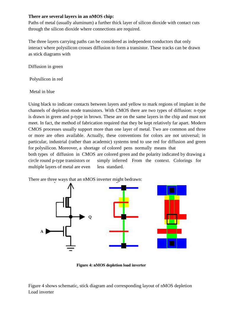
There are several layers in an nMOS chip:
Paths of metal (usually aluminum) a further thick layer of silicon dioxide with contact cuts
through the silicon dioxide where connections are required.
The three layers carrying paths can be considered as independent conductors that only
interact where polysilicon crosses diffusion to form a transistor. These tracks can be drawn
as stick diagrams with
Diffusion in green
Polysilicon in red
Metal in blue
Using black to indicate contacts between layers and yellow to mark regions of implant in the
channels of depletion mode transistors. With CMOS there are two types of diffusion: n-type
is drawn in green and p-type in brown. These are on the same layers in the chip and must not
meet. In fact, the method of fabrication required that they be kept relatively far apart. Modern
CMOS processes usually support more than one layer of metal. Two are common and three
or more are often available. Actually, these conventions for colors are not universal; in
particular, industrial (rather than academic) systems tend to use red for diffusion and green
for polysilicon. Moreover, a shortage of colored pens normally means that
both types of diffusion in CMOS are colored green and the polarity indicated by drawing a
circle round p-type transistors or simply inferred From the context. Colorings for
multiple layers of metal are even less standard.
There are three ways that an nMOS inverter might bedrawn:
Figure 4 shows schematic, stick diagram and corresponding layout of nMOS depletion
Load inverter

Figure 7 shows the stick diagram nMOS implementation of the function f=[(xy)+z]

Figure 8: stick diagram of CMOS NAND and NOR
Figure 8 shows the stick diagram CMOS NOR and NAND, where we can see that the p
diffusion line never touched the n diffusion directly, it is always joined using a blue color
metal line.
NMOS and CMOS Design style:
In the NMOS style of representing the sticks for the circuit, we use only NMOS transistor, in
CMOS we need to differentiate n and p transistor, that is usually by the color or in
monochrome diagrams we will have a demarcation line. Above the demarcation line are the
p transistors and below the demarcation are the n transistors.
Following stick shows CMOS circuit example in monochrome where we utilize the
demarcation line.
Figure 9 shows the stick diagram of dynamic shift register using CMOS style. Here the output of
the TG is connected as the input to the inverter and the same chain continues depending the
number of bits.

Design Rules:
Design rules include width rules and spacing rules. Mead and Conway developed a set of
simplified scalable λ -based design rules, which are valid for a range of fabrication
technologies. In these rules, the minimum feature size of a technology is characterized as 2 λ
. All width and spacing rules are specified in terms of the parameter λ . Suppose we have
design rules that call for a minimum width of 2 λ , and a minimum spacing of 3 λ . If
we select a 2 um technology (i.e., λ = 1 um), the above rules are translated to a
minimum width of 2 um and a minimum spacing of 3 um. On the other hand, if a 1 um
technology (i.e., λ = 0.5 um) is selected, then the same width and spacing rules are now
specified as 1 um and 1.5 um, respectively.
Figure 10 shows the design rule n diffusion, p diffusion, poly, metal1 and metal 2. The n and
p diffusion lines is having a minimum width of 2λand a minimum spacing of 3λ. Similarly
we are showing for other layers

.
Figure shows the design rule for the transistor, and it also shows that the poly should
extend for a minimum of 2λbeyond the diffusion boundaries.(gate over hang distance)
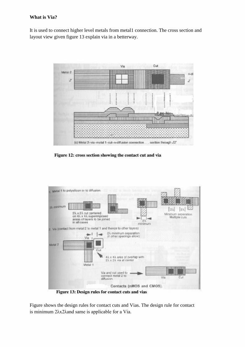
What is Via?
It is used to connect higher level metals from metal1 connection. The cross section and
layout view given figure 13 explain via in a betterway.
Figure shows the design rules for contact cuts and Vias. The design rule for contact
is minimum 2λx2λand same is applicable for a Via.

Buried contact: The contact cut is made down each layer to be joined and it is shown
in figure 14.
Butting contact: The layers are butted together in such a way the two contact cuts become
contiguous. We can better under the buttingcontact from figure

CMOS LAMBDA BASED DESIGN RULES:
Till now we have studied the design rules wrt only NMOS , what are the rules to be followed
if we have the both p and n transistor on the same chip will be made clear with the diagram.
Figure 16 shows the rules to be followed in CMOS well processes to accommodate both n
and p transistors.
Orbit 2µm CMOS process:
In this process all the spacing between each layersand dimensions will be in terms
micrometer. The 2µm here represents the feature size. All the design rules what ever we have
seen will not have lambda instead it will have the actual dimension in micrometer.
In one way lambda based design rules are better compared micrometer based design
rules, that is lambda based rules are feature size independent.
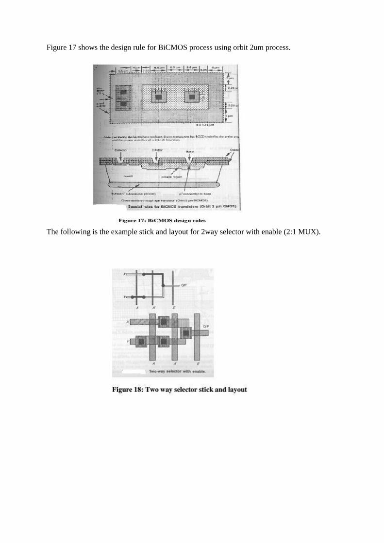
Figure 17 shows the design rule for BiCMOS process using orbit 2um process.
The following is the example stick and layout for 2way selector with enable (2:1 MUX).

Scaling of MOS Circuits:
What is Scaling?
Proportional adjustment of the dimensions of an electronic device while maintaining
the electrical properties of the device, results in a device either larger or smallerthan
the un-scaled device. Then Which way do we scale the devices for VLSI?
BIG and SLOW … or SMALLand FAST? What do we gain?
Why Scaling?...
Scale the devices and wires down, Make the chips ‘fatter’ – functionality, intelligence,
memory – and – faster, Make more chips per wafer – increased yield, Make the end user
Happy by giving more for less and therefore, make MORE MONEY!!
FoM for Scaling
Impact of scaling is characterized in terms of several indicators:
Minimum feature size
Number of gates on one chip
Power dissipation
Maximum operational frequency
Die size
Production cost
Many of the FoMs can be improved by shrinking the dimensions of transistors and
interconnections. Shrinking the separation between features – transistors and wires
Adjusting doping levels and supply voltages.
Technology Scaling :
Goals of scaling the dimensions by 30%:
Reduce gate delay by 30% (increase operating frequency by
43%) Double transistor density
Reduce energy per transition by 65% (50% power savings @ 43% increase in frequency)
Die size used to increase by 14% per generation
Technology generation spans 2-3 years

Figure1 to Figure 5 illustrates the technology scaling in terms of minimum feature
size, transistor count, prapogation delay, power dissipation and density and technology
generations.
Scaling Models
Full Scaling (Constant Electrical Field)
Ideal model – dimensions and voltage scale together by the same scale factor Fixed Voltage
Scaling
Most common model until recently – only the dimensions scale, voltages remain
constant General Scaling
Most realistic for today’s situation – voltages and dimensions scale with different factors
Scaling Factors for Device Parameters
Device scaling modeled in terms of generic scaling factors: 1/αand 1/β
• 1/β: scaling factor for supply voltage VDD, and gate oxide thickness D
• 1/α: linear dimensions both horizontal and vertical dimensions
Why is the scaling factor for gate oxide thickness different from other linear horizontal
and vertical dimensions? Consider the cross sectionof the device as in Figure 6,various
parameters derived are as follows.


Limitations of Scaling:
Effects, as a result of scaling down- which eventually become severe enough to prevent further
miniaturization.
• Substrate doping
• Depletion width
• Limits of miniaturization
• Limits of interconnect and contact resistance
• Limits due to sub threshold currents
• Limits on logic levels and supply voltage due to noise
• Limits due to current density

UNIT-III
GATE LEVEL DESIGN
LOGIC GATES AND OTHER COMPLEX GATES:
Invert(nmos, cmos, Bicmos) NAND Gate(nmos, cmos, Bicmos) NOR Gate(nmos, cmos, Bicmos)
The module (integrated circuit) is implemented in terms of logic gates and interconnections
between these gates. Designer should know the gate-level diagram of the design. In general, gate-level modeling is used for implementing lowest level modules in a design like, full-adder, multiplexers, etc.
nmos Inverter : The logic symbol and truth table of ideal inverter is shown in figure given below.
Here A is the input and B is the inverted output represented by their node voltages. Using positive logic,
the Boolean value of logic 1 is represented by Vdd and logic 0 is represented by 0. Vth is the inverter
threshold voltage, which is Vdd /2, where Vdd is the output voltage.
The output is switched from 0 to Vdd when input is less than Vth. So, for 0<Vin<Vth output is equal to logic 0
input and Vth<Vin< Vdd is equal to logic 1 input for inverter.
The characteristics shown in the figure are ideal. The nmos inverter is as shown

Let us consider the nmos inverter with 8:1 pull up transistors and 1:1 pull down transistors. Using this data,
the power dissipated by the inverter is obtained as
Rpu = Zpu * Rs = 8*10Kohms = 80 kΩ
Rpd = Zpd * Rs = 1*10Kohms = 10 kΩ
Assuming Vdd = 5V
(Power dissipated) Pd = V2/(Rpu + Rpd)
=25/(90 K Ω)
=o.28 nW
Further, as the pull down transistors shape-factor is ‘1’, the input capacitance is 1 Cg.
cmos Inverter : The CMOS inverter circuit is shown in the figure. Here, nMOS and pMOS transistors
work as driver transistors; when one transistor is ON, other is OFF.
This configuration is called complementary MOS (CMOS). The input is connected to the gate terminal of
both the transistors such that both can be driven directly with input voltages. Substrate of the nMOS is
connected to the ground and substrate of the pMOS is connected to the power supply, VDD.
So VSB = 0 for both the transistors.
VGS,n=VinVGS,n=Vin
VDS,n=VoutVDS,n=Vout
And,
VGS,p=Vin−VDDVGS,p=Vin−VDD
VDS,p=Vout−VDDVDS,p=Vout−VDD
When the input of nMOS is smaller than the threshold voltage (Vin < VTO,n), the nMOS is cut – off and
pMOS is in linear region. So, the drain current of both the transistors is zero.

ID,n=ID,p=0ID,n=ID,p=0
Therefore, the output voltage VOH is equal to the supply voltage.
Vout=VOH=VDDVout=VOH=VDD
When the input voltage is greater than the VDD + VTO,p, the pMOS transistor is in the cutoff region and the
nMOS is in the linear region, so the drain current of both the transistors is zero.
ID,n=ID,p=0ID,n=ID,p=0
Therefore, the output voltage VOL is equal to zero.
Vout=VOL=0Vout=VOL=0
The nMOS operates in the saturation region if Vin > VTO and if following conditions are satisfied.
VDS,n≥VGS,n−VTO,nVDS,n≥VGS,n−VTO,n
Vout≥Vin−VTO,nVout≥Vin−VTO,n
The pMOS operates in the saturation region if Vin < VDD + VTO,p and if following conditions are satisfied.
VDS,p≤VGS,p−VTO,pVDS,p≤VGS,p−VTO,p
Vout≤Vin−VTO,p
bicmos Inverter : A BiCMOS inverter, consists of a PMOS and NMOS transistor ( M2 and M1), two
NPN bipolar junction transistors,( Q2 and Q1), and two impedances which act as loads( Z2 and Z1) as shown in the circuit below.
When input, Vin, is high (VDD), the NMOS transistor ( M1), turns on, causing Q1 to conduct,while M2 and
Q2 are off, as shown in figure (b) . Hence , a low (GND) voltage is translated to the output Vout. On the
other hand, when the input is low, the M2 and Q2 turns on, while M1and Q1 turns off, resulting to a high
output level at the output as shown in Fig.(b). In steady-state operation, Q1 and Q2 never turns on or off
simultaneously, resulting to a lower power consumption. This leads to a push-pull bipolar output stage.

Transistors M1and M2, on the other hand, works as a phase-splitter, which results to a higher input
impedance.
The impedances Z2 and Z1 are used to bias the base-emitter junction of the bipolar transistor and to
ensure that base charge is removed when the transistors turn off. For example when the input voltage
makes a high-to-low transition, M1 turns off first. To turn off Q1, the base charge must be removed, which
can be achieved by Z1.With this effect, transition time reduces. However, there exists a short time when
both Q1 and Q2 are on, making a direct path from the supply (VDD) to the ground. This results to a current
spike that is large and has a detrimental effect on both the noise and power consumption, which makes
the turning off of the bipolar transistor fast .
nmos NAND Gate : vout <= vt = 0.2vdd
Vout = (vdd*n*zpd)/(nzpd+zpu) = 0.2vdd
= (nzpd)/(nzpd+zpu) = 0.2
Consider zpd = 1
(2)/(2+zpu) = 0.2
0.2zpu = 2-0.4
Zpu= 8
(zpu)/(2*zpd) = 8/2 = 4
nmos NAND geometry reveals two significant factors:

--nmos NAND gate area requirements are greater than those of a corresponding nmos inverter, pull
down transistors must be added in series to provide no.of inputs, as inputs are added there must be
corresponding length adjustment of pull up transistor, channel to maintain required overall ratio.
--nmos NAND gate delays are also increased in direct proportion to the members of required added.
If pull down transistor are kept at minimum size (2λx2λ) each will present 10’s CG at its inputs. But if their
n such inputs then the length and resistance by a factor n to keep correct ratio. Thus the delay associated
with nmos NAND are
ƬNAND = ƞ Tinv
Where , n- No. Of inputs
Tinv - Inverted delay
Other approach, keeping Zpu constant and widening pull down channels.
Nmos NAND gate is used only where absolutely necessary and when the number of inputs are restricted.
cmos NAND Gate : The two input NAND function is expressed by Y=A.B
Step 1 Take complement of Y
Y= A.B = A.B
Step 2 Design the PDN
In this case, there is only one AND term, so there will be two nMOSFETs in series as shown in figure.
Step 3 Design the PUN. In PUN there will be two pMOSFETs in parallel , as shown in figure
Finally join the PUN and PDN as shown in figure which realizes two –input NAND gate. Note that we have
realized y, rather tat Y because the inversion is automatically provided by the nature of the CMOS circuit
operation,
Working operation
1) Whenever at least one of the inputs is LOW, the corresponding pMOS transistor will conduct
while the corresponding nMOS transistor will turn OFF. Subsequently, the output voltage will be HIGH.
2) Conversely, if both inputs are simultaneously HIGH, then both pMOS transistors will turn
OFF, and the output voltage will be pulled LOW by the two conducting nMOS transistors.
The cmos NAND gate has no such restrictions but, bearing in mind the remarks are asymmetry,
it is necessary to allow for extended fall times on capacitive loads owing to the no.of n-transistors in series
forming the pull down. Some adjustments of transistor geometry is necessary for this reason and to keep
the transfer characteristics symmetrical above vdd/2.
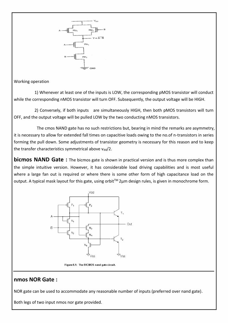
bicmos NAND Gate : The bicmos gate is shown in practical version and is thus more complex than
the simple intuitive version. However, it has considerable load driving capabilities and is most useful
where a large fan out is required or where there is some other form of high capacitance load on the
output. A typical mask layout for this gate, using orbitTM 2μm design rules, is given in monochrome form.
nmos NOR Gate :
NOR gate can be used to accommodate any reasonable number of inputs (preferred over nand gate).
Both legs of two input nmos nor gate provided.

The ratio must be such that one conducting pull down leg will give inverted line transfer characteristics.
Ares occupied by nmos NOR gate is reasonable since the pull up transistor dimensions are unaffected by
the number of inputs accommodate.
NOR gate is as fast as the inverter and is the preferred inverted based nmos logic.
cmos NOR Gate : The two input NOR function is expressed by
Y=A+B
Step 1: Take complement of Y
Y= A+B = A+B
Step 2: Design the PDN
In this case, there is only one OR term, so there will be two nMOSFETs connected in parallel, as shown in figure. Step 3: Design the PUN
In PUN there will be two pMOSFETs in series , as shown in figure NRI Institute of Technology
Finally join the PUN and PDN as shown in figure which realizes two –input NAND gate. Note that we have
realized y, rather tat Y because the inversion is automatically provided by the nature of the cMOS circuit
operation,
Working operation
1) Whenever at least one of the inputs is LOW, the corresponding pMOS transistor will conduct
while the corresponding nMOS transistor will turn OFF. Subsequently, the output voltage will be HIGH.
2) Conversely, if both inputs are simultaneously HIGH, then both pMOS transistors will turn
OFF, and the output voltage will be pulled LOW by the two conducting nMOS transistors.

Two pull up transistors are required to implement the logic ‘1’ condition and two pull down transistors
are required to implement logic ‘0’.
Pmos are connected in series, nmos are connected in parallel.
Predominant resistance of the p-devices is aggravated in its effect by the number connected in series.
Raise and fall time asymmetry on capacity load is increased and there will be a shift in the transfer
characteristics which will reduce noise immunity.
For these reasons CMOS NOR gate with more than 2 inputs may require adjustment if p,n transistors
geometry.
SWITCH LOGIC:
1) Switch logic is mainly based on pass transistor or transmission gate.
2) It is fast for small arrays and takes no static current from the supply, VDD. Hence power dissipation of such arrays is small since current only flows on switching.
3) Switch (pass transistor) logic is analogous to logic arrays based on relay contacts, where in path through each switch is isolated from the logic levels activating the switch.
PASS TRANSISTOR:
1) This logic uses transistors as switches to carry logic signals from node to node instead of connecting output nodes directly to VDD or ground(GND)
2) If a single transistor is a switch between two nodes, then voltage degradation.equal to Vt(threshold voltage) for high or low level depends up on nMOS or pMOS logic.
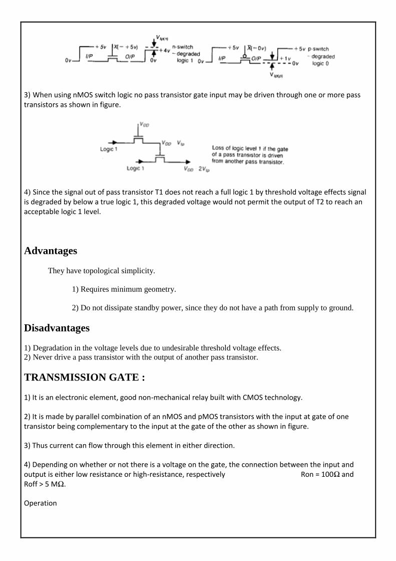
3) When using nMOS switch logic no pass transistor gate input may be driven through one or more pass transistors as shown in figure.
4) Since the signal out of pass transistor T1 does not reach a full logic 1 by threshold voltage effects signal is degraded by below a true logic 1, this degraded voltage would not permit the output of T2 to reach an acceptable logic 1 level.
Advantages
They have topological simplicity.
1) Requires minimum geometry.
2) Do not dissipate standby power, since they do not have a path from supply to ground.
Disadvantages
1) Degradation in the voltage levels due to undesirable threshold voltage effects.
2) Never drive a pass transistor with the output of another pass transistor.
TRANSMISSION GATE :
1) It is an electronic element, good non-mechanical relay built with CMOS technology.
2) It is made by parallel combination of an nMOS and pMOS transistors with the input at gate of one transistor being complementary to the input at the gate of the other as shown in figure.
3) Thus current can flow through this element in either direction.
4) Depending on whether or not there is a voltage on the gate, the connection between the input and output is either low resistance or high-resistance, respectively Ron = 100Ω and Roff > 5 MΩ.
Operation

• When the gate input to the nMOS transistor is ‘0’ and the complementary ‘1’ is gate input to the pMOS , thus both are turned off.
• When gate input to the nMOS is ‘1’ and its complementary ‘0’ is the gate input to the pMOS , both are turned on and passes any signal ‘1’ and ‘0’ equally without any degradation.
• The use of transmission gates eliminates the undesirable threshold voltage effects which give rise to loss of logic levels in pass-transistors as shown in figure.
Advantages
1) Transmission gates eliminates the signal degradation in the output logic levels.
2) Transmission gate consists of two transistors in parallel and except near the positive and negative
rails.
Disadvantages
1) Transmission gate requires more area than nMOS pass circuitry.
2) Transmission gate requires complemented control signals.
CMOS DOMINO LOGIC
Standard CMOS logic gates need a PMOS and an NMOS transistor for each logic input. The pMOS
transistors require a greater area tan the nMOS transistors carrying the same current. So, a large chip area is
necessary to perform complex logic operations. The package density in CMOS is improved if a dynamic
logic circuit, called the domino CMOS logic circuit, is used.
Domino CMOS logic is slightly modified version of the dynamic CMOS logic circuit. In this case, a
static inverter is connected at the output of each dynamic CMOS logic block. The addition of the inverter
solves the problem of cascading of dynamic CMOS logic circuits.
The circuit diagram of domino CMOS logic structures as shown in figure as follows

A domino CMOS AND-OR gate that realizes the function y = AB + CD is depicted in fugure . The left hand
part of the circuit containing Mn,Mp, T1,T2,,T3,and T4 forms and AND-ORINVERTER (AOI) gate. It
derives the static CMOS inverter formed by N2 and P2 in the right
hand part of the circuit. The domino gate is activated by the single phase clock ø applied to the NMOS (Mn)
and the PMOS (Mp) transistors. The load on the AOI part of the circuits is the parasitic load capacitance.
Working
• When ø = 0, is ON and Mn is OFF, so that no current flows in the AND-OR paths of the AOI. The
capacitor CL is charged to VDD through Mp since the latter is ON. The input to the inverter is high, and
drives the output voltage V0 to logic-0.
• When ø = 1, Mp is turned OFF and Mn is turned ON. If either (or both) A and B or C and D is at logic-1,
CL discharges through either T2,T1 and Mn or T3,T4 and Mp. So , the inverter input is driven to logic-0 and
hence the output voltage V0 to logic-1. The Boolean expression for the output voltage is Y = AB + CD.
Note : Logic input can change only when ø = 0. No changes of the inputs are permitted when ø = 1 since a
discharge path may occur.
Advantages
1) Smaller areas compared to conventional CMOS logic.
2) Parasitic capacitances are smaller so that higher operating speeds are possible.
3) Operation is free of glitches since each gate can make one transition.
Disadvantages
1) Non inverting structures are possible because of the presence of inverting buffer.
2) Charge distribution may be a problem.

CLOCKED CMOS LOGIC :
The clocked CMOS logic is also referred as C2MOS logic. Figure shows the general arrangement of a
clocked CMOS (C2MOS) logic. A pull-up p-block and a complementary n-block pull-down structure
represent p and n-transistors respectively and are used as implement clocked CMOS logic shown in figure.
However, the logic in this case is connected to the output only during the ON period of the clock. Figure
shows a clocked inverter circuit which is also belongs to clocked CMOS logic family. The slower rise times
and fall times can be expected due to owing of extra transistors in series with the output.
Working
• When ø = 1 the circuit acts an inverter , because transistors Q3 and Q4 are ‘ON’ . It is said to be in the
“evaluation mode”. Therefore the output Z changes its previous value.
• When ø = 0 the circuit is in hold mode, because transistors Q3 and Q4 becomes ‘OFF’ . It is said to be in
the “precharge mode”. Therefore the output Z remains its previous value
n-p CMOS LOGIC :
Figure shows the another variation of basic dynamic logic arrangement of CMOS logic called as n-p CMOS
logic. In this, logic the actual logic blocks are alternatively ‘n’ and ‘p’ in a cascaded structure. The clock ø
and ø- are used alternatively to fed the precharge and evaluate transistors. However, the functions of top and
bottom transistors are also alternate between precharge and evaluate transistors.

Working
• During the pre charge phase ø = 0 , the output of the n-tree gate, OUT 1 OUT3 , are charged to VDD,
while the output of the p-tree gate OUT2 is pre discharged to 0V. Since the n-tree gate connects pMOS
pull-up devices, the PUN of the p-tree is turned off at that time.
• During the evaluation phase ø = 1, the outputs (OUT1,OUT3) of the n-tree gate can only make a 1-Æ0
transition, conditionally turning on some transistors in the p-tree. This ensures that no accidental discharge
of OUT 2 can occur.
• Similarly n-tree blocks can follow p-tree gates without any problems, because the inputs to the n-gate are
pre charged to 0.
Disadvantages
Here, the p-tree blocks are slower than the n-tree modules, due to the lower current drive of the pMOS
transistors in the logic network.

UNIT-IV
ADDERS:
Binary Adder Notations and Operations:
As mentioned previously, adders in VLSI digital systems use binary notation.
In that case, add is done bit by bit using Boolean equations.
1-bit Half Adder.
Consider a simple binary add with two n-bit inputs A;B and a one-bit carry-in
cin along with n-bit output S.
S = A + B + Cin
Where A = an-1, an-2……a0; B = bn-1, bn-2……b0.
The + in the above equation is the regular and operation. However, in the
binary world, only Boolean algebra works. For add related operations, AND, OR and
Exclusive-OR (XOR) are required. In the following documentation, a dot between
two variables (each with single bit), e.g. a _ b denotes 'a AND b'. Similarly, a + b
denotes 'a OR b' and a _ b denotes 'a XOR b'. Considering the situation of adding two
bits, the sum s and carry c can be expressed
using Boolean operations mentioned above.
Si = ai ^ bi
Ci + 1 = ai . bi
The Equation of Ci+1 can be implemented as shown in Fig.2.1. In the figure,
there is a Half adder, which takes only 2 input bits. The solid line highlights the

critical path, which indicates the longest path from the input to the output. Equation of
ci+1 can be extended to perform full add operation, where there is a carry input.
Si = ai ^ bi ^ ci
Ci + 1 = ai . bi + ai . ci + bi . ci
1-bit Full Adder.
A Full adder can be built based on Equation above. The block diagram of a 1-
bit full adder is shown in Fig.2.2. The full adder is composed of 2 half adders and an
OR gate for computing carry-out. Using Boolean algebra, the equivalence can be
easily proven. To help the computation of the carry for each bit, two binary literals are
introduced. They are called carry generate and carry propagate, denoted by gi and pi.
Another literal called temporary sum ti is employed as well. There is relation between
the inputs and these literals.
Gi = ai . bi
Pi = ai + bi
Ti = ai ^ bi
Where i is an integer and 0 _ i < n.
With the help of the literals above, output carry and sum at each bit can be
written as:
Ci + 1 = gi + pi . ci
Si = ti ^ ci
In some literatures, carry-propagate pi can be replaced with temporary sum ti
in order to save the number of logic gates. Here these two terms are separated in order
to clarify the concepts. For example, for Ling adders, only pi is used as carry-
propagate.

The single bit carry generate/propagate can be extended to group version G
and P. The following equations show the inherent relations.
Gi : k = Gi : j + Pi : j . Gj – 1 : k
Pi : k = Pi : j . Pj-1:k
Where i : k denotes the group term from i through k.
Using group carry generate/propagate, carry can be expressed as expressed in
the following equation.
Ci + 1 = Gi : j + Pi : j . Cj
Ripple carry adder
Ripple carry adder is an n-bit adder built from full adders. Fig 2.1 shows a 4-bit ripple
carry adder. One full adder is responsible for the addition of two binary digits at any
stage of the ripple carry. The carryout of one stage is fed directly to the carry-in of
the next stage. Even though this is a simple adder and can be used to add unrestricted
bit length numbers, it is however not very efficient when large bit numbers are used.
4-b Ripple Carry Adder
One of the most serious drawbacks of this adder is that the delay increases
linearly with the bit length. The worst-case delay of the RCA is when a carry
signal transition ripples through all stages of adder chain from the least significant
bit to the most significant bit, which is approximated by:
T = (n-1) tc + ts
Delay :

The latency of a 4-bit ripple carry adder can be derived by considering the
worst-case signal propagation path. We can thus write the following
expressions:
TRCA-4bit = TFA(A0,B0→Co)+T FA (C in→C1)+TFA (Cin→C2)+ TFA
(Cin→S3)
And, it is easy to extend to k-bit RCA:
TRCA-4bit = TFA(A0,B0→Co)+(K-2)* TFA (Cin→Ci)+ TFA (Cin→Sk-1).
Drawbacks :
Delay increases linearly with the bit length and Not very efficient when large
bit numbers are used.
Carry Look-Ahead Adder
Lookahead carry algorithm speed up the operation to perform addition,
because in this algorithm carry for the next stages is calculated in advance based on
input signals. In CLA, the carry propagation time is reduced to O(log2(Wd)) by using
a tree like circuit to compute the carry rapidly. Fig. shows the 4-bit Carry Look-Ahead
Adder.
4-bit Carry Look Ahead Adder
The CLA exploits the fact that the carry generated by a bit-position depends
on the three inputs to that position. If ‘X’ and ‘Y‘ are two inputs then if X=Y=1, a
carry is generated independently of the carry from the previous bit position and if

X=Y= 0, no carry is generated. Similarly if X ≠ Y, a carry is generated if and only if
the previous bit-position generates a carry. ‘C’ is initial carry, “S” and “Cout” are
output sum and carry respectively, then Boolean expression for calculating next carry
and addition is:
Pi = Xi xor Yi -- Carry Propagation
Gi = Xi and Yi -- Carry Generation
Ci + 1 = Gi or (Pi and Ci) -- Next Carry
Si = Xi xor Yi xor Ci -- Sum Generation
Thus, for 4-bit adder, we can extend the carry, as shown below:
C1 = G0 + P0 · C0
C2 = G1 + P1 · C1 = G1 + P1 · G0 + P1 · P0 · C0
C3 = G2 + P2 · G1 + P2 · P1 · G0 + P2 · P1 · P0 · C0
C4 = G3 + P3 · G2 + P3 · P2 · G1 + P3 · P2 · P1 · G0+ P3 · P2 · P1 · P0 · C0
As with many design problems in digital logic, we can make tradeoffs
between area and performance (delay). In the case of adders, we can create faster (but
larger) designs than the RCA. The Carry Look ahead Adder (CLA) is one of these
designs (there are others too, but we will only look at the CLA).
Drawbacks :
For long bit length, a carry look-ahead adder is not practical, but a hierarchical
structure one can improve much. The disadvantage of CLA is that the carry logic
block gets very complicated for more than 4-bits. For that reason, CLAs are usual
implemented as 4-bit modules and are used in a hierarchical structure to realize adders
that have multiples of 4-bits.
Carry Save Adder
The carry-save adder reduces the addition of 3 numbers to the addition of 2
numbers. The propagation delay is 3 gates regardless of the number of bits. The carry-
save unit consists of n full adders, each of which computes a single sum and carries
bit based solely on the corresponding bits of the three input numbers.

The entire sum can then be computed by shifting the carry sequence left by
one place and appending a 0 to the front (most significant bit) of the partial sum
sequence and adding this sequence with RCA produces the resulting n+1-bit value.
This process can be continued indefinitely, adding an input for each stage of
full adders, without any intermediate carry propagation. These stages can be arranged
in a binary tree structure, with cumulative delay logarithmic in the number of inputs
to be added, and invariant of the number of bits per input. The main application of
carry save algorithm is, well known for multiplier architecture is used for efficient
CMOS implementation of much wider variety of algorithms for high speed digital
signal processing .CSA applied in the partial product line of array multipliers will
speed up the carry propagation in the array.
4-bit Carry Save Adder
Basically, carry save adder is used to compute sum of three or more n-bit
binary numbers. Carry save adder is same as a full adder. As shown in the Fig.2.4,
here we are computing sum of two 4-bit binary numbers, so we take 4 full adders at
first stage. Carry save unit consists of 4 full adders, each of which computes single
sum and carry bit based only on the corresponding bits of the two input numbers. Let
X and Y are two 4-bit numbers and produces partial sum and carry as S and C as
shown in the below :
Si = Xi xor Yi ; Ci = Xi and Yi
The final addition is then computed as:

1. Shifting the carry sequence C left by one place.
2. Placing a 0 to the front (MSB) of the partial sum sequence S.
3. Finally, a ripple carry adder is used to add these two together and computing the
resulting sum.
Carry Save Adder Computation :
X: 1 0 0 1 1
Y: 1 1 0 0 1
Z: + 0 1 0 1 1
S: 0 0 0 0 1
C: + 1 1 0 1 1
SUM: 1 1 0 1 1 1
In this design 128 bit carry save adder is used since the output of the multiplier
is 128 bits (2N). The carry save adder minimize the addition from 3numbers to 2
numbers. The propagation delay is 3gates despite of the number of bits. The carry
save adder contains n full adders, computing a single sum and carries bit based mainly
on the respective bits of the three input numbers. The entire sum can be calculated by
shifting the carry sequence left by one place and then appending a 0 to most
significant bit of the partial sum sequence. Now the partial sum sequence is added
with ripple carry unit resulting in n + 1 bit value. The ripple carry unit refers to the
process where the carryout of one stage is fed directly to the carry in of the next stage.
This process is continued without adding any intermediate carry propagation. Since
the representation of 128 bit carry save adder is infeasible, hence a typical 8 bit carry
save adder is shown in the figure 3.Here we are computing the sum of two 128 bit
binary numbers, then 128 half adders at the first stage instead of 128 full adder.
Therefore , carry save unit comprises of 128 half adders, each of which computes
single sum and carry bit based only on the corresponding bits of the two input
numbers.

bit carry save adder
If x and y are supposed to be two 128 bit numbers then it produces the partial
products and carry as S and C respectively.
Si = xi 1\ yi (4)
Ci = xi & yi (5)
During the addition of two numbers using a half adder, two ripple carry adder
is used. This is due the fact that ripple carry adder cannot compute a sum bit without
waiting for the previous carry bit to be produced, and hence the delay will be equal to
that of n full adders. However a carry-save adder produces all the output values in
parallel, resulting in the total computation time less than ripple carry adders. So,
Parallel In Parallel Out (PIPO) is used as an accumulator in the final stage.
2.5. Carry Select Adder
A carry-select adder is divided into sectors, each of which – except for the
least-significant –performs two additions in parallel, one assuming a carry-in of zero,
the other a carry-in of one. A four bit carry select adder generally consists of two
ripple carry adders and a multiplexer. The carry-select adder is simple but rather fast,
having a gate level depth of O(√n) . Adding two n-bit numbers with a carry select

adder is done with two adders (two ripple carry adders) in order to perform the
calculation twice, one time with the assumption of the carry being zero and the other
assuming one.
After the two results are calculated, the correct sum, as well as the correct
carry, is then selected with the multiplexer once the correct carry is known. The
design schematic of Carry Select Adder is shown in Fig.
The N-bit Ripple Carry Adder constructed by N set single bit Full-adder
In the N-bit carry ripple adder, the delay time can be expressed as:
TCRA = (N-1) Tcarry + Tsum
In the N-bit carry select adder, the delay time is:
TCSA = Tsetup + (N/M) Tcarry + MTmux + Tsum
In our proposed N-bit area-efficient carry select adder, the delay time is:
Tnew = Tsetup + (N-1) Tmux + Tsum
The carry select adder comes in the category of conditional sum adder.
Conditional sum adder works on some condition. Sum and carry are calculated by
assuming input carry as 1 and 0 prior the input carry comes. When actual carry input
arrives, the actual calculated values of sum and carry are selected using a multiplexer.
The conventional carry select adder consists of k/2 bit adder for the lower half
of the bits i.e. least significant bits and for the upper half i.e. most significant bits
(MSB’s) two k/bit adders. In MSB adders one adder assumes carry input as one for

performing addition and another assumes carry input as zero. The carry out calculated
from the last stage i.e. least significant bit stage is used to select the actual calculated
values of output carry and sum. The selection is done by using a multiplexer. This
technique of dividing adder in two stages increases the area utilization but addition
operation fastens.
2.6 Ripple Carry Adder
The basic addition operation at the bit level can be accomplished with a Full
Adder (FA) circuit. FA adds two input bits Xi and Yi along with an input carry Cin ,
resulting in a sum Si and a carry-out bit Cout as shown in Figure 3(b). The operation
preformed by the FA is defined by the following boolean equations for the sum and
the carry-out bits:
Si = Xi ⊕ Yi ⊕ Cin
Cout = (Xi ∧ Yi) ∨ (Cin ∧ (Xi ⊕ Yi))
= Majority(Xi, Yi, Cin)
The following notation for various Boolean operators will be used in this work to
avoid ambiguity
x ∨ y ↔ x OR y
x ∧ y ↔ x AND y
x ⊕ y ↔ x XOR y
x ↔ NOT x
It is apparent from equations 2.4 and 2.5 that the realization of the sum function
requires two XOR logic gates, while two AND and one OR logic gates are needed for
the carry-out function. Despite that, FA sum and carry-out functions can be
represented in many different logic expressions and, thereby, determine the structure
of the circuit. Based upon those different logic expressions, many full-adder cells and
modules can be conceived. This provides the digital designer with various alternatives
for the FA adder implementations to choose from and to investigate. Recently Shams
et al. carried out detailed performance analysis of twenty three 1-bit FA. Their study

showed that each adder cell exhibits it own figurers of power consumption, delay and
area.the area and power-delay product performance of six existing 1-bit FA adders
and proposed a new design based on XOR/XNOR. proposed five different FA
expressions based on XOR/XNOR implementation to explore different performance
tradeoffs. Then, they used their proposed FA cells to improve the area and power of
an array tree multiplier.
The 1-bit FA is cascaded as illustrated in Figure 4 to create n-bit wide operand adder
known as Ripple Carry Adder (RCA). The sum at each bit position i is determined by
the corresponding bit values of the operands at that position and the incoming carry
bit value from (i − 1)th position. The addition is completed once the carry value
propagates along the entire structure to the most significant bit (MSB) position.
Ripple carry adder block diagram.
The area and delay of this adder can be roughly estimated using the unit-gate delay
and area model. This model is technology independent and assumes that each gate,
excluding exclusive-OR, counts as one elementary gate for both area and delay. An
exclusive-OR gate counts for two elementary gates for both area and delay.
Complex gates as well as multi-input gates are built from 2-input basic gates and their
gate count equals the sum of gate counts of the composing cells. Thus, RCA delay is
estimated as 2n unit-gate delay while its area is 7n unit-gate area, where n is the
operand size. The main advantage of RCA implementation is that it is area efficient
and easy to construct. However, its linear delay characteristics makes it less suitable
for high-speed implementations. An improved addition approach in given next.

Multipliers
Introduction
Multiplication is important fundamental function in arithmetic logic operation. A
system’s performance is generally determined by the performance of the multiplier
because the multiplier is generally the slowest clement in the system. The objective of
good multiplier to provide a physically compact high speed and low power
consumption unit.To reduce significant power consumption of multiplier design it is a
good direction to reduce number of operations thereby reducing a dynamic power
which is a major part of total power dissipation.
An efficient multiplier should have following characteristics:-
Accuracy:- A good multiplier should give correct result.
Speed:- Multiplier should perform operation at high speed.
Area:- A multiplier should occupies less number of slices and LUTs.
Power:- Multiplier should consume less power.
Multiplication process or A multiplier can be divided into three steps-
1. Partial product generation-The first is radix 4 booth encoding in which a partial
product is produced from the multiplier and multiplicand.
2. Partial product reduction-The second is adder array or partial product compression
to add all partial products and convert them into the form of sum and carry.
3. Final addition-The last is the final addition in which the final multiplication result
is generated by adding the sum and carry . Z=A*B+Z.
For the multiplication of an n-bit multiplicand with an m bit multiplier, m partial
products are generated and products formed is n + m bits long.

A=(an an-1 an-2.......................a0) B=(bn bn-1 bn-2.....................b0)
AB= ( A2nbn+A2n-1bn-1+A2n-2bn-2+...................................+A20b0 )
Types of Multipliers
The common multiplication method is “add and shift” algorithm.
1.) In parallel multipliers number of partial products to be added is the main
parameter that determines the performance of the multiplier.
2.)To reduce the number of partial products to be added, Modified Booth algorithm is
one of the most popular algorithms.
3.)To achieve speed improvements Wallace Tree algorithm can be used to reduce the
number of sequential adding stages.
4.) On the other hand “serial-parallel” multipliers compromise speed to achieve better
performance for area and power consumption. The selection of a parallel or serial
multiplier actually depends on the nature of application.
Applications
1.)Multiplication is a heavily used arithmetic operation that figures prominently in
signal processing and scientific applications
2.)Multipliers are key components of many high performance systems such as FIR
filters, microprocessors, digital signal processors, etc.
3.) Multipliers play an important role in today’s digital signal processing and various
other applications.

Types of Multipliers
Serial-Parallel Multiplier
The serial multiplier uses successive addition algorithm, where both operands are
entered in serial manner, which leads to poor speed performance. However in the
parallel multiplier both operands are entered in parallel manner, which gives high

speed but occupies much larger area when compared to serial multiplier.Hence, we go
for serial-parallel multiplier.
The serial-parallel multiplier serves as a good trade-off between the time consuming
serial multiplier and area consuming parallel multipliers. These multipliers are used
when there is demand for both high speed and small area. In a device using the serial-
parallel multiplier, one operand is entered serially and the other operand is stored in
parallel with a fixed number of bits. The resultant enhancement in the processing
speed and the chip area will become more significant when a large number of
independent operations are performed.
1.)This multiplier is the simplest one, the multiplication being considered as a
succession of additions.
If A=(an an-1 an-2.......................a0)
B=(bn bn-1 bn-2..............b0)
then the product A.B may be expressed as
AB= ( A2nbn+A2n-1bn-1+A2n-2bn- 2+...................................+A20b0 )
2.)To implement this we use D flip-flop and full adder .
3.)In this D flip-flop acts as a memory to store the data values and full adder circuit
is used for adding the partial products.
4.)A possible form of this multiplier for multiplying 4- bit quantities based on this
expression is shown in figure (1). The operation of the multiplier is as follows-
i.)'Number A' is entered in the 4 right most bits of the top row of D flip-flop, which
are further connected to three D flip-flops to form a 7-bit shift register. The first left
most column of D flip-flops holds B values.
ii.) The number A( a3 a2 a1 a0 ) is then multiplied with the least significant bit of
B( b0 ). Later the number A is shifted and then multiplied with the other bits of B one
after the other simultaneously.The partial products are then added using full adders.
iii.)This is done to allow the multiplication of 'number A' by 21 22..................2n, thus
forming the partial product at each stage of the process.
5.)This approach can be used to eliminate the least significant bits of the product.
6.)A further reduction in hardware can be done by using 3 additional D flip-flops
( which were earlier used as shifting of A proceeds ) for holding b values.
7.)This structure is suited only for positive or unsigned operands. If the operands are
negative and 2's compliment encoded then -

i.) The most significant bit of B will have a negative weight and so a subtraction must
be performed as the last step.
ii.) The most significant bit of A must be replicated since operand A must be
expanded to 2N bits.
Figure (1): 4- bit Serial and Parallel Multiplier
Braun Multiplier
Braun Edward Louis proposed the braun multiplier in 1963. It is the simplest parallel
multiplier, that is commonly known as the Carry Save Array Multiplier.
This multiplier consists of an array of AND gates and adders arranged in an iterative
structure that does not require logic registers. This is also known as the non-additive
multiplier since it does not add an a operand to result of the multiplication. The
completion time is limited by the depth of the Carry Save Array, and by the Carry
propagation in the adder.This multiplier is suited only for positive operands. This
multiplier is restricted to performing multiplication of two unsigned numbers.

Architecture
1.)An n*n bit Braun multiplier is constructed with n (n-1) adders, n2 AND gates and
(n-1) rows of Carry Save Adder .
2.)In the first rows there is no Carry propagation ( using Carry Save adder).At the
bottom of the array, the output of the array is noted in Carry Save, so an adder
converts it ( by mean of a Carry propagation) into the classical notation.
3.)Each products can be generated in parallel with the AND gates. Each partial
product can be added to the previous sum of partial products.(which has produced by
using the row of adders).
4.)The carry out will be shifted one bit to the left or right and then are added to the
sum of first adder and the newly generated partial product.
5.)The shifting would carry out with the help of Carry Save Adder (CSA) and the
Ripple carry adder should be used for the final stage of the output.
6.)The schematic diagram is as shown figure(4.2).
Figure - Carry save adder
Figure - Ripple Carry adder


Performance of Braun Multiplier
1.)Braun multiplier performs well for the unsigned operands that are less than 16 bits
in terms of speed, power and area.But it is simple structure when compared to the
other multipliers.
2.)The number of components required in building the Braun multiplier increases
quadratically with the number of bits, which makes it inefficient.
3.)The main drawback of this multiplier is that the potential susceptibility of glitching
problem due to the Ripple Carry Adder in the last stage. The delay depends on the
delay of the Full Adder and also a final adder in the last stage.
To overcome drawback
1.)The internal structure of the full adder can be realized using FPGA. The power and
area can also be reduced by using two bypassing techniques called Row bypassing
technique and Column bypassing technique.
2.)Delay due to the final ripple adder can be minimized by using very fast one of a
Parallel Prefix Adder “KOGGE STONE ADDER” which is a type of Carry Look
Head Adder.
Speed consideration:
1.)The delay of the Braun multiplier is dependent on the delay of the full Adder cell
and also on the final Adder in the last row.
2.)In the multiplier array, a full Adder with balanced Carry and sum delays is
desirable because the sum and carry signals are both in the critical path.
3.)The speed and power of the full Adder is very important for large arrays.
Enhanced Braun Multipliers
1.)The performance of Braun Multiplier can be enhanced by replacing full adders
with half adder, which will result in saving three logic gates, but regularity of
structure gets disturbed.
2.)The another way to do this is by optimising the interconnection between the adders,
so that delay through out each adders path is approximately same.

Baugh-Wooley multiplier
In signed multiplication the length of the partial products and the number of partial
products will be very high. So an algorithm was introduced for signed multiplication
called as Baugh- Wooley algorithm. The Baugh-Wooley multiplication is one
amongst the cost-effective ways to handle the sign bits. This method has been
developed so as to style regular multipliers, suited to 2's compliment numbers.
Baugh-Wooley Two’s compliment Signed multipliers is the best known algorithm for
signed multiplication because it maximizes the regularity of the multiplier and allow
all the partial products to have positive sign bits.
Figure- unsigned 4-
bit multiplication
Figure-signed 4-bit multiplication
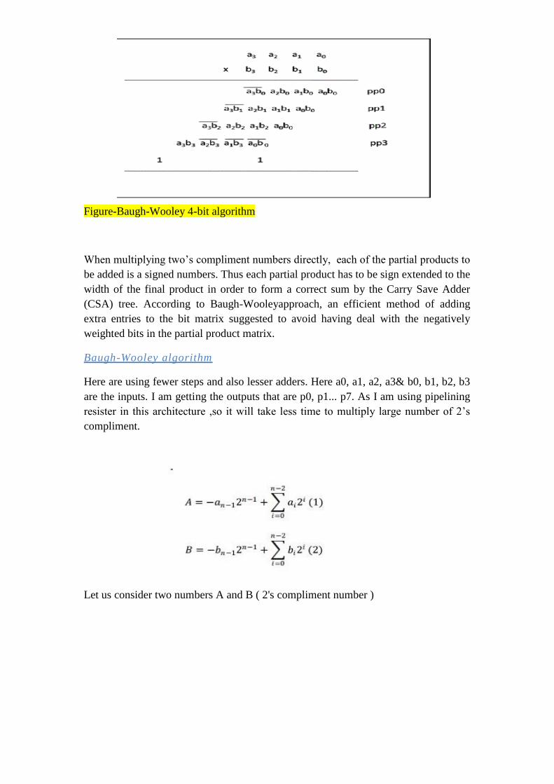
Figure-Baugh-Wooley 4-bit algorithm
When multiplying two’s compliment numbers directly, each of the partial products to
be added is a signed numbers. Thus each partial product has to be sign extended to the
width of the final product in order to form a correct sum by the Carry Save Adder
(CSA) tree. According to Baugh-Wooleyapproach, an efficient method of adding
extra entries to the bit matrix suggested to avoid having deal with the negatively
weighted bits in the partial product matrix.
Baugh-Wooley algorithm
Here are using fewer steps and also lesser adders. Here a0, a1, a2, a3& b0, b1, b2, b3
are the inputs. I am getting the outputs that are p0, p1... p7. As I am using pipelining
resister in this architecture ,so it will take less time to multiply large number of 2’s
compliment.
Let us consider two numbers A and B ( 2's compliment number )

The product of two numbers is
--->(3)
The first two terms of above equation are positive and last two terms are negative.
The last two terms are n-1 bits that extend in binary weight from 2n-1 upto 22n-3.O n
the other hand, the final product is 2n bits that extends in binary weight from 20 to
22n-1 . In order to calculate the product, instead of subtracting the last two terms, it is
possible to add the opposite values.
We see that subtractor cells must be used. In order to use only adder cells, the
negative terms may be rewritten as :
----->(4)
Then A.B becomes
---->(5)
The final equation is

----->(6)
The above equation signifies the Baugh-Wooley algorithm for multiplication process
in two’s compliment form.
Baugh-Wooley Multiplier provides a high speed, signed multiplication algorithm . It
uses parallel products to complement multiplication and adjusts the partial products to
maximize the regularity of multiplication array . When number is represented in two’s
complement form, sign of the number is embedded in Baugh-Wooley multiplier.This
algorithm has the advantage that the sign of the partial product bits are always kept
positive so that array addition techniques can be directly employed.In the two’s
complement multiplication, each partial product bit is the AND of a multiplier bit and
a multiplicand bit, and the sign of the partial product bits are positive .In this scheme ,
a total of n(n - 1) + 3 full adders are required. Hence, for the case of n = 4, the array
requires 15 adders.


FPGA AND CPLDS
Integrated circuits (IC) technology is the enabling technology for a whole host
of innovative devices and systems that have changed the way of living. VLSI systems
are much smaller and consume less power than discrete components used to built
electronic systems before 1960’s. The electronics industry has achieved a phenomenal
growth over the last two decades, mainly due to the rapid advances in integration
technologies, large-scale systems design in short, due to the advent of VLSI. The
number of applications of integrated circuits in high-performance computing,
telecommunications, and consumer electronics has been rising steadily, and at a very
fast pace. Typically, the required computational power (or, in other words, the
intelligence) of these applications is the driving force for the fast development of this
field. Below figure gives an overview of the prominent trends in information
technologies over the next few decades. The current leading-edge technologies (such
as low bit-rate video and cellular communications) already provide the end-users a
certain amount of processing power and portability.
Trends of VLSI
This trend is expected to continue, with very important implications on VLSI
and systems design. One of the most important characteristics of information services
is their increasing need for very high processing power and bandwidth (in order to
handle real-time video, for example). The other important characteristic is that the
information services tend to become more and more personalized (as opposed to
collective services such as broadcasting), which means that the devices must be more

intelligent to answer individual demands, and at the same time they must be portable
to allow more flexibility/mobility. As more and more complex functions are required
in various data processing and telecommunications devices, the need to integrate
these functions in a small system/package is also increasing. The level of integration
as measured by the number of logic gates in a monolithic chip has been steadily rising
for almost three decades, mainly due to the rapid progress in processing technology
and inter connect technology.
Figure 6.2: Evolution of integration density and minimum feature size, as seen in the
early 1980s.
2. VLSI Design Flow
The design process at various levels is usually evolutionary in nature. It starts
with a given set of requirements. Initial design is developed and tested against the
requirements. When requirements are not met, the design has to be improved. If such
improvement is either not possible or too costly, then the revision of requirements and
its impact analysis must be considered. The three important domains in VLSI are
Behavioral domain, Structural domain, Geometrical layout domain. The design flow
starts from the algorithm that describes the behavior of the target chip. The
corresponding architecture of the processor is first defined. It is mapped onto the chip
surface by floor planning. The next design evolution in the behavioral domain defines

finite state machines (FSMs) which are structurally implemented with functional
modules such as registers and arithmetic logic units (ALUs).
These modules are then geometrically placed onto the chip surface using CAD
tools for automatic module placement followed by routing, with a goal of minimizing
the interconnects area and signal delays. The third evolution starts with a behavioral
module description. Individual modules are then implemented with leaf cells. At this
stage the chip is described in terms of logic gates (leaf cells), which can be placed and
interconnected by using a cell placement & routing program. The last evolution
involves a detailed Boolean description of leaf cells followed by a transistor level
implementation of leaf cells and mask generation. In standard-cell based design, leaf
cells are already pre-designed and stored in a library for logic design use.
3. Design Hierarchy
The use of hierarchy, or divide and conquer technique involves dividing a
module into sub- modules and then repeating this operation on the sub-modules until
the complexity of the smaller parts becomes manageable. This approach is very
similar to the software case where large programs are split into smaller and smaller
sections until simple subroutines, with well-defined functions and interfaces, can be
written. The design of a VLSI chip can be represented in three domains.
Correspondingly, a hierarchy structure can be described in each domain separately.
However, it is important for the simplicity of design that the hierarchies in different
domains can be mapped into each other easily.
In the physical domain, partitioning a complex system into its various
functional blocks will provide a valuable guidance for the actual realization of these
blocks on chip. Obviously, the approximate shape and size (area) of each sub-module
should be estimated in order to provide a useful floor plan. This physical view
describes the external geometry of the adder, the locations of input and output pins,
and how pin locations allow some signals (in this case the carry signals) to be
transferred from one sub-block to the other without external routing.

4.VLSI Design Styles
Several design styles can be considered for chip implementation of specified
algorithms or logic functions. Each design style has its own merits and shortcomings,
and thus a proper choice has to be made by designers in order to provide the
functionality at low cost.
Field Programmable Gate Array (FPGA)
Fully fabricated FPGA chips containing thousands of logic gates or even more,
with programmable interconnects, are available to users for their custom hardware
programming to realize desired functionality. This design style provides a means for
fast prototyping and also for cost-effective chip design, especially for low-volume
applications. A typical field programmable gate array (FPGA) chip consists of I/O
buffers, an array of configurable logic blocks (CLBs), and programmable interconnect
structures. The programming of the inter connects is implemented by programming of
RAM cells whose output terminals are connected to the gates of MOS pass
transistors.
Performance of the design can be simulated and verified before downloading
the design for programming of the FPGA chip. The programming of the chip remains
valid as long as the chip is powered-on or until new programming is done. In most
cases, full utilization of the FPGA chip area is not possible - many cell sites may
remain unused.
The largest advantage of FPGA-based design is the very short turn-around
time, i.e., the time required from the start of the design process until a functional chip
is available. Since no physical manufacturing step is necessary for customizing the
FPGA chip, a functional sample can be obtained almost as soon as the design is
mapped into a specific technology. The typical price of FPGA chips are usually higher
than other realization alternatives (such as gate array or standard cells) of the same
design, but for small-volume production of ASIC chips and for fast prototyping,
FPGA offers a very valuable option.

General architecture of Xilinx FPGA.
Gate Array Design
In view of the fast prototyping capability, the gate array (GA) comes after the
FPGA. While the design implementation of the FPGA chip is done with user
programming, that of the gate array is done with metal mask design and processing.
Gate array implementation requires a two-step manufacturing process: The first phase,
which is based on generic (standard) masks, results in an array of uncommitted
transistors on each GA chip. These uncommitted chips can be stored for later
customization, which is completed by defining the metal interconnects between the
transistors of the array. Since the patterning of metallic interconnects is done at the
end of the chip fabrication, the turn-around time can be still short, a few days to a few
weeks.
Basic processing steps required for gate array implementation.

Figure above shows a magnified portion of the internal array with metal mask
design (metal lines highlighted in dark) to realize a complex logic function. Typical
gate array platforms allow dedicated areas, called channels. The availability of these
routing channels simplifies the interconnections, even using one metal layer only. The
interconnection patterns to realize basic logic gates can be stored in a library, which
can then be used to customize rows of uncommitted transistors according to the net
list. While most gate array platforms only contain rows of uncommitted transistors
separated by routing channels, some other platforms also offer dedicated memory
(RAM) arrays to allow a higher density where memory functions are required.
Layout views of a conventional GA chip and a gate array with two memory banks.
Metal mask design to realize complex logic function on channeled GA
In general, the GA chip utilization factor, as measured by the used chip area
divided by the total chip area, is higher than that of the FPGA and so is the chip speed,

since more customized design can be achieved with metal mask designs. The current
gate array chips can implement as many as hundreds of thousands of logic gates.
Standard-Cells Based Design
The standard-cells based design is one of the most prevalent full custom
design styles which require development of a full custom mask set. For instance, the
inverter gate can have standard size transistors, double size transistors, and quadruple
size transistors so that the chip designer can choose the proper size to achieve high
circuit speedandlayoutdensity.
The standard cell is also called the poly cell. In this design style, all of the
commonly used logic cells are developed, characterized, and stored in a standard cell
library. A typical library may contain a few hundred cells including inverters, NAND
gates, NOR gates, complex AOI, OAI gates, D-latches, and flip-flops. Each gate type
can have multiple implementations to provide adequate driving capability for
different fan outs.
VHDL contains constructs that are more specific to simulation and verification
than for synthesis. Synthesis software may ignore such constructs or rules. However,
the goal is to match the simulation specification with the codes for synthesis.
Depending on tools, the goal may (or usually) not be achievable. For example, the
following two VHDL codes are different but describe the same design - one for
simulation (cannot be synthesized efficiently) and the other for synthesis.
A standard cell layout example.
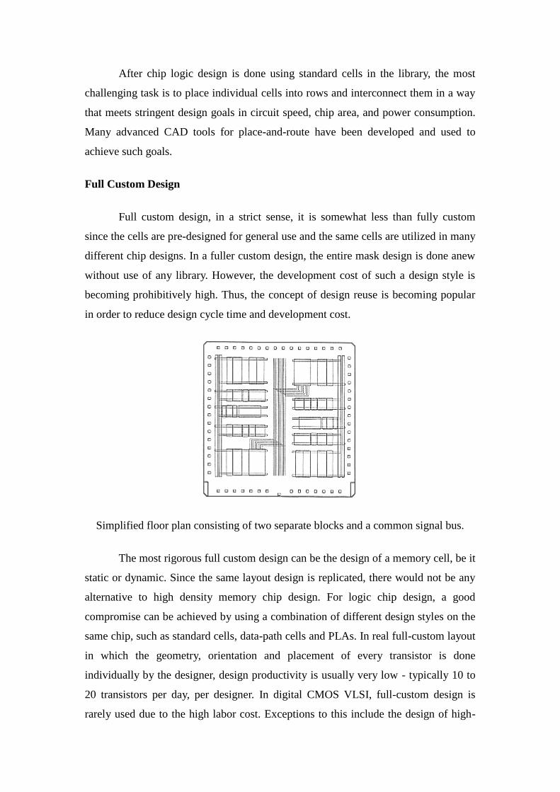
After chip logic design is done using standard cells in the library, the most
challenging task is to place individual cells into rows and interconnect them in a way
that meets stringent design goals in circuit speed, chip area, and power consumption.
Many advanced CAD tools for place-and-route have been developed and used to
achieve such goals.
Full Custom Design Full custom design, in a strict sense, it is somewhat less than fully custom
since the cells are pre-designed for general use and the same cells are utilized in many
different chip designs. In a fuller custom design, the entire mask design is done anew
without use of any library. However, the development cost of such a design style is
becoming prohibitively high. Thus, the concept of design reuse is becoming popular
in order to reduce design cycle time and development cost.
Simplified floor plan consisting of two separate blocks and a common signal bus.
The most rigorous full custom design can be the design of a memory cell, be it
static or dynamic. Since the same layout design is replicated, there would not be any
alternative to high density memory chip design. For logic chip design, a good
compromise can be achieved by using a combination of different design styles on the
same chip, such as standard cells, data-path cells and PLAs. In real full-custom layout
in which the geometry, orientation and placement of every transistor is done
individually by the designer, design productivity is usually very low - typically 10 to
20 transistors per day, per designer. In digital CMOS VLSI, full-custom design is
rarely used due to the high labor cost. Exceptions to this include the design of high-

volume products such as memory chips, high- performance microprocessors and
FPGA masters.
Cost of Manufacturing
IC manufacturing plants are extremely expensive. A single plant costs as
much as $4 billion. Given that a new state –of-the-art manufacturing process is
developed every three years that is a sizeable investment. The investment makes sense
because s single plant can manufacture so many chips and can easily be switched to
manufacture different types of chips. In early years of the IC business companies
focused on building large quantities of a few standard parts. These parts are
commodities one 80 ns, 256 MB dynamic RAM is one more or less the same as any
other regardless of the manufacturer. Companies concentrated on commodity parts
because manufacturing variations are easier to keep track of when the same part is
being fabricated day after day. Standard parts also made sense because designing
integrated circuits was hard not only the circuit but the layout had to be designed, and
there were few computer programs to help automate the design process.

UNIT-5


CIRCUIT SYNTHESIS AND DESIGNFLOW:


SIMULATION: