university of nairobieie.uonbi.ac.ke/sites/default/files/cae/engineering/eie/smoke...
TRANSCRIPT

UNIVERSITY OF NAIROBI
COLLEGE OF ARCHITECTURE AND ENGINEERING
SCHOOL OF ENGINEERING
DEPARTMENT OF ELECTRICAL AND INFORMATION
ENGINEERING
PROJECT: SMOKE ALARM
PROJECT NUMBER: 107
NAME: NG’ANG’A RENSON NGOCHI
REG. NO: F17/1421/2011
SUPERVISOR: DR. C.W. WEKESA
EXAMINER: PROF. M. K. MANG’OLI

i
A project report submitted to the Department of Electrical and
Information Engineering in partial fulfilment of the requirements for the
award of BSc. Electrical and Electronic Engineering of the University of
Nairobi.

ii
DECLARATION OF ORIGINALITY
NAME: NG‟ANG‟A RENSON NGOCHI
REGISTRATION NUMBER: F17/1421/2011
COLLEGE: Architecture and Engineering
SCHOOL: Engineering
DEPARTMENT: Electrical and Information Engineering
COURSE NAME: BSc. Electrical and Electronic Engineering
PROJECT: SMOKE ALARM
1) I understand what plagiarism is and I am aware of the University policy on this
regard.
2) I declare that this final year project is my original work and has not been
submitted elsewhere for examination, award of degree or publication. Where other
people‟s work or my own work has been used, this has properly been
acknowledged and referenced in accordance with University of Nairobi‟s
requirements.
3) I have not sought or used the services of any professional agencies to produce
this work.
4) I have not allowed and shall not allow anyone to copy my work with the
intention of passing it off as his/her own work.
5) I understand that any false claim in respect of this work shall result in
disciplinary action, in accordance with University anti-plagiarism policy.

iii
Signature:
……………………………………..……………………………………...................
..
Date:
……………………………………..………………………………………………
….

iv
DECLARATION AND CERTIFICATION This is my original work and has not been presented for any degree award in this or any other
university. Information from other sources has been duly acknowledged.
…………………………………………………………………………
NG‟ANG‟A RENSON NGOCHI
F17/1421/2011
This report has been submitted to the Department of Electrical and Information Engineering,
University of Nairobi with my approval as supervisor:
……………………………………………………………………………..
DR. C. W. Wekesa
Date: ………………………….

v
`DEDICATION This project is dedicated to my parents, James Ng‟ang‟a Mwangi and Martha
Wamaitha Ng‟ang‟a and my siblings, Catherine Nyambura, Martin Mwangi and
Caroline Wairimu for their unwavering financial and emotional support as well as
undying love and encouragement throughout my academic journey.

vi
ACKNOWLEDGEMENT First, I would like to thank the Almighty God for granting me life and good health
as well as supreme protection and guidance throughout my studies.
I am thankful to my supervisor, Dr. C. W. Wekesa for his informative and useful
guidance and suggestions throughout the journey for project design.
I am very grateful to the Department of Electrical and Information Engineering and
my lecturers for instilling in me the knowledge that has brought me this far.
I am thankful to my friends and classmates who have contributed to the success of
my studies through their wise counsel and support.
Needless to mention, this project would not have been complete without reference
to and inspiration from the work of others whose details are included in the
reference section of this document.

vii
Table of Contents DECLARATION OF ORIGINALITY ............................................................................................................... ii
DECLARATION AND CERTIFICATION ........................................................................................................ iv
`DEDICATION ........................................................................................................................................... v
ACKNOWLEDGEMENT ............................................................................................................................ vi
Table of Figures ...................................................................................................................................... ix
CHAPTER 1: INTRODUCTION .................................................................................................................... 1
1.1 BACKGROUND ............................................................................................................................... 1
1.2 PROBLEM STATEMENT ................................................................................................................... 2
1.3 OBJECTIVES .................................................................................................................................... 2
1.4 SCOPE OF WORK ............................................................................................................................ 2
CHAPTER 2: LITERATURE REVIEW ............................................................................................................ 3
2.1 LDR-BASED SMOKE DETECTOR ....................................................................................................... 4
2.2 PHOTO INTERRUPTER MODULE-BASED SMOKE SENSOR ................................................................ 5
2.3 RE46C190 PHOTOELECTRIC SMOKE DETECTOR .............................................................................. 9
2.4 SMOKE DETECTOR WITH GAS SENSOR TGS 813 ............................................................................ 10
2.5 MQ2 SENSOR-BASED SMOKE DETECTOR ...................................................................................... 13
CHAPTER 3: REVIEW OF COMPONENTS USED ........................................................................................ 16
3.1 MQ2 SMOKE SENSOR ................................................................................................................... 16
3.2 ATMEGA 32A ............................................................................................................................... 20
3.3 LCD MODULE ............................................................................................................................... 24
3.4 BUZZER ........................................................................................................................................ 30
3.5 LED .............................................................................................................................................. 30
3.6 POWER SUPPLY MODULE ............................................................................................................. 31
CHAPTER 4: DESIGN ............................................................................................................................... 34
4.1 HARDWARE DESIGN ..................................................................................................................... 35
4.1.1 MQ2 SENSOR ........................................................................................................................ 35
4.1.2 ATMEGA 32A......................................................................................................................... 36
4.1.3 INTERFACING LCD TO ATMEGA 32A ...................................................................................... 36
4.1.4 VISUAL ALARM (LEDs) ........................................................................................................... 39
4.1.5 AUDIO ALARM (BUZZER) ....................................................................................................... 40
4.2 SOFTWARE DESIGN ...................................................................................................................... 42
4.2.1 ADC PROGRAM ..................................................................................................................... 43

viii
4.2.2 LCD PROGRAM ...................................................................................................................... 45
4.2.3 ALARM ACTIVATION PROGRAM ............................................................................................ 45
4.3 PCB DESIGN ................................................................................................................................. 46
CHAPTER 5: RESULTS ............................................................................................................................. 47
5.1 SIMULATED RESULTS ................................................................................................................... 47
5.3 RESULTS AFTER IMPLEMENTATION .............................................................................................. 50
CHAPTER 6: CONCLUSION AND RECOMMENDATION ............................................................................. 55
6.1 CONCLUSION ............................................................................................................................... 55
6.2 RECOMMENDATIONS................................................................................................................... 56
References ............................................................................................................................................ 57
APPENDIX 1: CIRCUIT DIAGRAM ............................................................................................................ 58
APPENDIX 2: ATMEGA 32A BLOCK DIAGRAM ......................................................................................... 60
APPENDIX 3: C PROGRAM ...................................................................................................................... 61
APPENDIX 4: COST ................................................................................................................................. 64

ix
Table of Figures Figure 1Symbol of LDR ............................................................................................................................. 4
Figure 2 Schematic and block diagram of LDR based smoke detector ....................................................... 5
Figure 3 Symbol ofPhotointerrupter ........................................................................................................ 6
Figure 4 Pin diagram of Photo Interrupter Module .................................................................................. 6
Figure 5 Photo interrupter module .......................................................................................................... 6
Figure 6 Typical photo interrupter circuit for digital logic ......................................................................... 7
Figure 7 Block Diagram for LM 555 .......................................................................................................... 8
Figure 8 Connection diagram for 555 timer as an Astable Multivibrator ................................................... 9
Figure 9RE46C190 application circuit [5] ................................................................................................ 10
Figure 10 TGS 813 configuration [6] ....................................................................................................... 11
Figure 11 TGS 813 Diagram for Electric Circuit [6] .................................................................................. 11
Figure 12 Basic Measuring Circuit with TGS sensor [6] ........................................................................... 12
Figure 13 MQ2 sensor ........................................................................................................................... 14
Figure 14 Connection diagram for MQ2 sensor ...................................................................................... 15
Figure 15 Structure of MQ2 [7] .............................................................................................................. 18
Figure 16 ATmega 32A ........................................................................................................................... 20
Figure 17 Pinout PDIP ATmega 32A [8] .................................................................................................. 23
Figure 18 LCD image .............................................................................................................................. 25
Figure 19 Buzzer .................................................................................................................................... 30
Figure 20 Electronic Symbol for LED....................................................................................................... 30
Figure 21 Parts of an LED ....................................................................................................................... 31
Figure 22: FLOWCHART FOR PROJECT DESIGN PROCESS ........................................................................ 34
Figure 23: MQ2 SENSOR ........................................................................................................................ 35
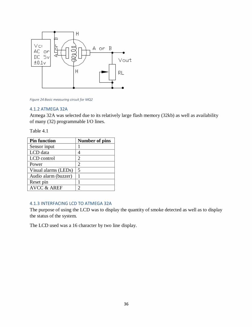
Figure 24 Basic measuring circuit for MQ2 ............................................................................................. 36
Figure 25:Microcontroller-LCD interface simulation ............................................................................... 39
Figure 26 Microcontroller - LEDs interface simulation ............................................................................ 40
Figure 27 Final design of smoke sensor (Excluding the power supply) .................................................... 41
Figure 28 FLOWCHART FOR SOFTWARE DESIGN .................................................................................... 42
Figure 29 :LCD DISPLAY IN SMOKE DETECTED MODE SIMULATION ........................................................ 48
Figure 30: LCD DISPLAY IN STANDBY MODE SIMULATION ...................................................................... 49
Figure 31Final Circuit with power switched off ...................................................................................... 50
Figure 32 Circuit on breadboard with INSIGNIFICANT quantity of smoke detected ................................. 51
Figure 33Final Circuit with INSIGNIFICANT quantity of smoke detected ................................................. 52
Figure 34 Circuit on Breadboard with SIGNIFICANT quantity of smoke detected .................................... 53
Figure 35 Final Circuit with SIGNIFICANT quantity of Smoke Detected ................................................... 54

1
CHAPTER 1: INTRODUCTION
1.1 BACKGROUND
A smoke alarm is a device that senses smoke, typically as an indicator of fire. It
may issue a signal to a fire alarm control panel as part of fire alarm system,
especially in commercial security devices or may issue a local audible or visual
alarm in the household [1].
Fire detection has become a crucial aspect in design of buildings, both commercial
and domestic, as opposed to about 70 years ago when automatic detection was
rarely provided in buildings. Before introduction of smoke and fire alarms, fires
resulted in the loss of human lives and damage of property and it was mainly
attributed to lack of a mechanism for early detection of fire. Early developments in
design of smoke alarm began in 1922 with observations by Greinacher and later by
Walter Jaeger in 1930. However, early smoke detectors required high voltage
power input. Further research was done and power requirement in smoke detectors
was reduced to make battery power viable and this made widespread installation in
residences highly feasible. Later developments in smoke detectors have sought to
improve their performance, reduce power requirement, improve their nuisance
alarm sensitivity and also to continuously monitor their status. The most recent
advances in smoke detectors have been motivated to make them „smarter‟ [2].
Smoke can be detected either optically (photoelectric) or by physical process
(ionization). Detectors may use either or both methods.
Smoke detectors have prior detection when compared with heat detectors, hence
are preferred for fire detection. They also find application in detecting, and thus
deter smoking in premises where it is banned.

2
1.2 PROBLEM STATEMENT
Safety is a crucial consideration in design of residential and commercial buildings
in order to safeguard against loss of life and damage to property. Fire is a key
element in safety considerations.
This project therefore seeks to design a microcontroller based smoke alarm that
will continuously monitor the presence of significant amount of smoke and activate
an alarm to prompt a safety measure to contain the situation. There is also an extra
functionality of LCD display for visual alert.
1.3 OBJECTIVES
The main objective of this project is to design a circuit useful for detecting smoke
and activating an alarm. To achieve this, the following must be done:
a) Analysis and calibration of MQ2 smoke sensor.
b) Development of program to convert the analog output of the sensor to
equivalent digital form in the microcontroller.
c) Development of visual warnings (LCD and LED) to indicate smoke
detection.
d) Development of audio warnings (buzzer) to indicate the presence of smoke.
1.4 SCOPE OF WORK
The scope of this project is to design a circuit for smoke detection. It activates an
alarm when a substantive quantity of smoke is sensed. Hence, it does not primarily
indicate the presence of fire.

3
CHAPTER 2: LITERATURE REVIEW A smoke detector is a device that senses smoke typically as an indicator of fire or
non-smoking zone.
In order to ensure human safety and safeguard property against fire in both
domestic and commercial settings, different solutions for smoke detection have
been developed. These designs vary depending on the method of smoke detection.
However, the different designs are derived from the two basic types of smoke
detectors, namely: 1.The photoelectric smoke detector
2. The ionization chamber smoke detector (ICSD)
The photoelectric smoke detector uses an optical beam to search for smoke. When
smoke particles cloud the beam, a photoelectric cell senses the decrease in light
intensity and triggers an alarm. This type of smoke detector reacts most quickly to
smoldering fires that release relatively large amounts of smoke.
On the other hand, the ionization chamber smoke detector is quicker at sensing
flaming fires that produce little smoke. It employs a radioactive material to ionize
the air in a sensing chamber; the presence of smoke affects the flow of the ions
between a pair of electrodes, which triggers the alarm [3] . In a typical system, the
radioactive material emits alpha particles that strip electrons from the air
molecules, creating positive oxygen and nitrogen ions. The electrons attach
themselves to other air molecules, forming negative oxygen and nitrogen ions.
Two oppositely charged electrodes within the sensing chamber attract the positive
and negative ions, setting up a small flow of current in the air space between the
electrodes, but when the smoke particles enter the chamber, they attract some of
the ions, disrupting the current flow. There is usually a similar chamber
constructed so that no smoke particles can enter, so that the smoke detector

4
constantly compares the current flow in the sensing chamber to the flow in the
reference chamber; if a significant difference develops, an alarm is triggered. This
is the most commonly used design for domestic smoke detection.
2.1 LDR-BASED SMOKE DETECTOR
LDR (Light Dependent Resistor) also known as a LDR, photo resistor,
photoconductor or photocell, is a resistor whose resistance increases or decreases
depending on the amount of light intensity. LDRs are usually made of many semi-
conductive materials with high resistance. The reason they have a high resistance is
that there are very few electrons that are free and able to move because they are
held in crystal lattice and are unable to move. When light falls on the semi
conductive material, it absorbs the light photons and the energy is transferred to the
electrons, which allow them to break free from the crystal lattice and conduct
electricity and lower the resistance of the LDR. In addition to fire and smoke
alarms, it finds uses in photographic light meters and street lights.
Figure 1Symbol of LDR
This detector relies on the smoke that is produced in the event of a fire and passes
between a bulb and an LDR, the amount of light falling on the LDR decreases
hence its resistance increases. This in turn affects its voltage characteristics which
can be used to pull high the voltage at the base of a transistor to which the supply
to the chip on board is completed. The sensitivity of the smoke detector depends on
the distance between bulb and LDR. Its working is as illustrated in the figure
below.

5
Figure 2 Schematic and block diagram of LDR based smoke detector
2.2 PHOTO INTERRUPTER MODULE-BASED SMOKE SENSOR
Photo interrupter comprises of an infrared LED which is called the emitter (E) and
a phototransistor called the detector (D). Both devices are housed in the same
package so no mechanical adjusting is needed. On the side of the transistor there is
a daylight blocking filter to make the photo interrupter less sensitive to ambient
light. Apart from usage in smoke alarm, it can be used in controlling the position of
a moving part (to check if the part is in desired position or not) or you can count
pulses from a rotating index disc to measure the rpm of your motor (rotary
encoder).
Chip on
Board (COB)
voltage
regulator
Audio
amplifier Speaker

6
Figure 3 Symbol ofPhotointerrupter
Figure 4 Pin diagram of Photo Interrupter Module
Figure 5 Photo interrupter module
A photo transistor works like a normal transistor but instead of a current at the
base, it requires light to turn on the collector-emitter current flow. In a photo
interrupter the LED and the photo transistor are mounted in small posts and when
nothing interrupts the beam, the transistor turns on, passing a current from the
collector to the emitter. When the beam is interrupted, say, by smoke, the transistor
turns off.

7
A photo interrupter has four leads or connectors: anode and cathode for the LED
and collector and emitter for the photo transistor.
A typical connection of the photo interrupter is as shown in the Figure 4.
Figure 6 Typical photo interrupter circuit for digital logic
In the circuit diagram above, resistor, R1, limits the current to the LED to atypical
value of about 20mA. R3 should not be more than 100k as this can lead to
additional problems because of the high impedance of the circuit.
Ambient light can cause reaction on the detector. The effect can be reduced by
choosing a photo interrupter with the minimum gap width that is possible in the
application. When you can‟t get rid of ambient light, then the resistors should be
adjusted accordingly.
When there is no obstruction in the photo interrupter, the light coming from the
LED falls directly onto the photo transistor, this makes the collector terminal to go

8
ground potential. The output tapped at the collector of the photo transistor reads 0
(LOW)
When there is smoke in the vicinity, it blocks the beam from reaching the photo
transistor which in turns reduces its conductivity to ground highly and the output
voltage at its collector is 5V(HIGH).
This collector terminal is then connected to the reset control of 555 timer.
Figure 7 Block Diagram for LM 555
The 555 timer is wired as astable multivibrator as shown in the next figure.

9
Figure 8 Connection diagram for 555 timer as an Astable Multivibrator
With the duty cycle, usually set at 50% for optimum performance, the resistors and
capacitor are carefully selected using the following relations:
Duty cycle = ((R1+R2)/ (R1+2*R2))*100%
Frequency, f =1.443/ ((R1+2*R2)*C)
The high voltage at the reset pin enables the ic and it produces square wave
continuously through pin3, which in turns drives the speaker or buzzer through a
coupling capacitor. The astable is usually configured as an oscillator with a
frequency in the audio range (20Hz-20kHz).
2.3 RE46C190 PHOTOELECTRIC SMOKE DETECTOR
The RE46C190 is a low voltage, low current programmable photoelectric smoke
detector IC. With minimal external components, this smoke detector alarm circuit
can provide all the required features for a photoelectric smoke detector type
electronic project. Programmable setup, calibration and feature selection are the
key to reduced component count and cost. The boost regulator insures proper
operation of the infrared diode and the piezo horn under low battery conditions.
The design incorporates a gain-selectable photo amplifier for use with an infrared
emitter detector pair. An internal oscillator strobes power to the smoke detection
circuitry every 10 seconds, to keep the standby current to a minimum. If smoke is
sensed, the detection rate is increased to verify an alarm condition. [4]

10
Figure 9RE46C190 application circuit [5]
2.4 SMOKE DETECTOR WITH GAS SENSOR TGS 813
TGS 813 is a general purpose sensor which has good sensitivity characteristics to a
wide range of gases including methane, propane, butane and other combustible
gases.
It is designed to operate with a stabilized 5V heater supply and a circuit voltage not
exceeding 24V. These voltage ratings are very practical when determining the
design specifications, which make it highly economical.
The circuit also has a very short initial stabilization time and the relative and
elapsed characteristics are very good over a long period of operation. It also has a
very low sensitivity to „noise gases‟ which reduces the problem of nuisance
alarming significantly.

11
Figure 10 TGS 813 configuration [6]
Figure 11 TGS 813 Diagram for Electric Circuit [6]
The TGS 813 is a bulk semiconductor composed mainly of tio dioxide with
electrodes and the heater coil located inside the ceramic former.

12
Figure 12 Basic Measuring Circuit with TGS sensor [6]
The variation in resistance of the TGS sensor is measured directly as a change in
voltage appearing across the load resistor. In fresh air, the current passing through
the sensor and RL in series is steady, but when smoke or combustible gases come
into contact with the sensor surface, the sensor resistance decreases in accordance
with the concentration of the gas present. The voltage across RL is the same when
VC and VH are supplied from AC or DC sources. The output voltage can then be
utilized to trigger an alarm.
However, the sensor resistance is dependent upon the ambient temperature and
humidity, a phenomenon that will result in fluctuation of the alarming point.
Hence, when designing, it is recommended that we determine the mean or average
temperature and humidity values in the area of operation, to be able to compensate
for seasonal variations in the alarming point. To compensate or this, a negative
characteristic thermistor can be used. Another point of consideration is the actual
place where the thermistor is placed in the circuit. It shouldn‟t be installed near
heat dissipating components such as the transformer or the sensor. Also, it should
not be installed in position where it is likely to receive a strong wind, as this will
also affect the temperature characteristics of the sensor. [6]

13
2.5 MQ2 SENSOR-BASED SMOKE DETECTOR
The MQ 2 sensor belongs to the MQ series Semiconductor Gas Sensors.
The MQ sensor find application in gas leak and smoke detection application. Their
major advantageous features include:
High sensitivity
Fast response
Wide detection range
Stable performance and long life
Simple drive circuit
The following table shows the various MQ series sensors and target gas of
detection
Model Target Gas
MQ2 General combustible gas including
smoke.
MQ3 Alcohol
MQ4 Natural gas, Methane
MQ5 LPG, Natural gas, Coal gas
MQ6 LPG, Propane
MQ7 Carbon Monoxide
MQ8 Hydrogen
MQ9 CO and Combustible gas
MQ216 Natural gas\ Coal gas
MQ306A LPG, Propane
MQ309A CO, Flammable gas
MQ303A Alcohol
MQ131 Ozone O3
MQ135 Air Quality Control(NH3, Benzene,
Alcohol, Smoke)
MQ136 H2S
MQ137 Ammonia
MQ138 Mellow, Benzene, Aldehyde, Ketone,
Ester
MQ2 is the most suitable and readily available for smoke detection.

14
Figure 13 MQ2 sensor
MQ2 is a flammable gas and smoke sensor which detects the concentrations of
combustible gas in the air and outputs reading as an analog voltage. It is sensitive
to a wide range of gases and are used at room temperature.
Some modules have a built-in variable resistor to adjust the sensitivity of the
sensor.
It falls under the category of electromechanical gas detectors which work by
allowing gases to diffuse through a porous membrane to an electrode where it is
either chemically oxidized or reduced. The amount of current produced is
determined by how much of the gas is oxidized at the electrode, indicating
concentration of the gas. However, this type of sensors is subject to corrosive
elements or chemical contamination and may last only 1-2 years before a
placement is required.
For MQ2, the sensitive material used is SnO2, whose conductivity is lower in clean
air. Its conductivity increases as the concentration of combustible gases increases.

15
Figure 14 Connection diagram for MQ2 sensor
The output voltage, which is analogue in nature, can be used to activate a buzzer
by interfacing it with a microcontroller, Arduino or Raspberry Pi.
For the purpose of design of the smoke detector circuit for this project,
the MQ2 sensor was chosen due to the following advantageous features:
Wide detecting scope
Availability
Stable and long life
Fast response
Low cost
Simple drive circuit

16
CHAPTER 3: REVIEW OF COMPONENTS USED This chapter focuses on various components and elements that have been used
in the project. These include:
1) MQ2 smoke sensor
2) Atmega 32A
3) LCD module
4) Buzzer
5) LED
6) Power supply module
3.1 MQ2 SMOKE SENSOR
MQ2 sensors are used in gas leakage detecting equipment in family and industry,
and are suitable for detecting LPG, i-butane, propane, methane ,alcohol, Hydrogen,
smoke.
3.1.1 Features
Wide detecting scope Fast response and High sensitivity Stable and long life Simple drive circuit
3.1.2 Specifications A. Standard work condition
Symbol Parameter name Technical condition Remarks
Vc Circuit voltage 5V±0.1 AC OR DC
VH Heating voltage 5V±0.1 ACOR DC
RL Load resistance can adjust
RH Heater resistance 33Ω±5% Room Tem
PH Heating consumption less than 800mw
B. Environment condition
Symbol Parameter name Technical condition Remarks
Tao Using Tem -20-50
Tas Storage Tem -20-70
RH Related humidity less than 95%Rh
O2 Oxygen
concentration
21%(standard
condition)Oxygen
concentration can
minimum value
is over 2%

17
affect sensitivity
C. Sensitivity characteristic
Symbol Parameter
name
Technical parameter Remarks
Rs Sensing
Resistance
3KΩ-30KΩ
(1000ppm iso-butane )
Detecting
concentration
scope:
200ppm-
5000ppm LPG and propane 300ppm-5000ppm
butane 5000ppm-20000ppm methane 300ppm-5000ppm H2
100ppm-2000ppm
Alcohol
Α
(3000/1000)
isobutane
Concentration
Slope rate
≤0.6
Standard
Detecting
Condition
Temp: 20±2 Vc:5V±0.1
Humidity: 65%±5% Vh: 5V±0.1
Preheat
time
Over 24 hour
[7]
D Structure and configuration, basic measuring circuit

18
Figure 15 Structure of MQ2 [7]
Parts Materials
1 Gas sensing layer SnO2
2 Electrode Au (Gold)
3 Electrode line Pt (Platinum)
4 Heater coil Nickel-Chromium alloy
5 Tubular ceramic Al2O3
6 Anti-explosion Stainless steel gauze
7 Clamp ring Copper plating, Ni
8 Resin base Bakelite
9 Tube pin Copper plating, Ni
3.1.3 Precautions
Following conditions must be prohibited
Exposure to organic silicon steam
Organic silicon steam cause sensors invalid. Sensors must be not be exposed to
silicon bond, silicon latex, putty or plastic contain silicon environment.
High Corrosive gas

19
If the sensors exposed to high concentration corrosive gas (such as H2Sz, SOX,Cl2
,HCl etc), it will not only result in corrosion of sensors structure, also it cause
severe sensitivity attenuation.
Alkali, Alkali metals salt, halogen pollution
The sensors performance will be changed badly if sensors be sprayed polluted by
alkali metals salt especially brine, or be exposed to halogen such as fluorine.
Touch water
Sensitivity of the sensors will be reduced when spattered or dipped in water.
Freezing
Freezing causes the sensor to lose sensitivity.
Applied voltage higher
Applied voltage on sensor should not be higher than stipulated value, otherwise it
would cause down-line or heater damage, and cause sensors’ sensitivity
characteristic alteration.
Voltage on wrong pins
This would lead to lead breakage, hence damage the functionality of the sensor.
Following conditions must be avoided
Water Condensation
Under indoor conditions, slight water condensation will effect sensors
performance lightly. However, if water condensation on sensors surface occurs
over a prolonged period, sensor’ sensitivity will be decreased.
Used in high gas concentration
Whether it is powered or not, prolonged exposure to high gas concentration will
affect sensors characteristic adversely.
Long time storage
The sensors resistance produce reversible drift if it’s stored for long time without powering. For the sensors with long time storage with no powering, they may require aging time for stability before using.
Long time exposed to adverse environment
Exposure to adverse environment for long time, such as high humidity, high
temperature, or high pollution, it will affect the sensors performance adversely.

20
Vibration
Continual vibration will result in sensors down-lead response then. Transportation
or assembling line, pneumatic screwdriver/ultrasonic welding machine can lead
this vibration.
Concussion
If sensors meet strong concussion, it may lead its lead wire disconnected.
3.2 ATMEGA 32A
Microcontroller is basically a computer on a chip. It is a compact microcomputer,
designed to control the operation of embedded electronic systems in various
applications such as motor vehicles, home appliances, office machines, robots,
medical devices, vending machines, mobile radio transceivers, and other electronic
devices. Typically, a microcontroller comprise of a processor, timers, memory,
clock/oscillator, and other peripherals. The difference between a microcontroller
and a microprocessor is that a microprocessor is an integrated circuit that only has
CPU but no memory as in the microcontroller. They are used in general purpose
applications.
The Atmel ATmega32A is a low-power CMOS 8-bit microcontroller based on the
AVR enhanced RISC architecture. The device is manufactured using Atmel‟s high
density nonvolatile memory technology.
Figure 16 ATmega 32A
Features

21
High-performance, Low-power Atmel AVR 8-bit Microcontroller
Advanced RISC Architecture
-131 Powerful Instructions - Most Single-clock Cycle Execution
-32 × 8 General Purpose Working Registers
-Fully Static Operation
-Up to 16MIPS Throughput at 16MHz
-On-chip 2-cycle Multiplier
High Endurance Non-volatile Memory segments
-32 Kbytes of In-System Self-programmable Flash program memory
-1024 Bytes EEPROM
-2 Kbytes Internal SRAM
-Write/Erase cycles: 10,000 Flash/100,000 EEPROM
-Data retention: 20 years at 85°C/100 years at 25°C(1)
-Optional Boot Code Section with Independent Lock Bits
In-System Programming by On-chip Boot Program
True Read-While-Write Operation
-Programming Lock for Software Security
JTAG Interface
-Boundary-scan Capabilities According to the JTAG Standard
-Extensive On-chip Debug Support
-Programming of Flash, EEPROM, Fuses and Lock Bits through the JTAG
Interface
Peripheral Features
-Two 8-bit Timer/Counters with Separate Prescalers and Compare Modes
-One 16-bit Timer/Counter with Separate Prescaler, Compare Mode, and Capture
Mode

22
-Real Time Counter with Separate Oscillator
-Four PWM Channels
-8- channel, 10-bit ADC
8 Single-ended Channels
7 Differential Channels in TQFP Package Only
Differential Channels with Programmable Gain at 1x, 10x, or 200x
-Byte-oriented Two-wire Serial Interface
-Programmable Serial USART
-Master/Slave SPI Serial Interface
-Programmable Watchdog Timer with On-chip Oscillator
-On-chip Analog Comparator
I/O and Packages
-32 Programmable I/O Lines
-40-pin PDIP, 44-lead TQFP, and 44-pad QFN/MLF
Operating Voltages
-2.7 - 5.5V
Speed Grades
-0 -16MHz
Power Consumption at 1MHz, 3V, 25°C
-Active: 0.6mA
-Idle Mode: 0.2mA
-Power-down Mode: < 1μA

23
Figure 17 Pinout PDIP ATmega 32A [8]
VCC
This is the digital supply voltage.
GND
This is the ground pin.
Port A (PA7:PA0)
Port A serves as the analog inputs to the A/D Converter. Port A also serves as an 8-
bit bi-directional I/O port, if the A/D Converter is not used.
Port B (PB7:PB0)
Port B is an 8-bit bi-directional I/O port with internal pull-up resistors (selected for
each bit).
Port C (PC7:PC0)
Port C is an 8-bit bi-directional I/O port with internal pull-up resistors (selected for
each bit). If the JTAG interface is enabled, the pull-up resistors on pins PC5(TDI),
PC3(TMS) and PC2(TCK) will be activated even if a reset occurs.
The TD0 pin is tristated unless TAP states that shift out data are entered.
Port D (PD7:PD0)

24
Port D is an 8-bit bi-directional I/O port with internal pull-up resistors (selected for
each bit).
RESET
This is the reset input. A low level on this pin for longer than the minimum pulse
length will generate a reset, even if the clock is not running. The minimum pulse
length is given in System and Reset Characteristics. Shorter pulses are not
guaranteed to generate a reset.
XTAL1
Input to the inverting Oscillator amplifier and input to the internal clock operating
circuit.
XTAL2
Output from the inverting Oscillator amplifier.
AVCC
AVCC is the supply voltage pin for Port A and the A/D Converter. It should be
externally connected to VCC, even if the ADC is not used. If the ADC is used, it
should be connected to VCC through a low-pass filter.
AREF
AREF is the analog reference pin for the A/D Converter.
3.3 LCD MODULE
A liquid-crystal display (LCD) is a flat-panel display or other electronic visual
display that uses the light-modulating properties of liquid crystals.
The LCD screen is more energy-efficient and can be disposed of more safely than
a CRT. Its low electrical power consumption enables it to be used in battery-
powered electronic equipment more efficiently than CRTs. It is an electronically
modulated optical device made up of any number of segments controlling a layer
of liquid crystals and arrayed in front of a light source (backlight) or reflector to
produce images in color or monochrome. [9]

25
Figure 18 LCD image
The 1602A QAPASS module was used in this project.
Mechanical Dimension
Item Dimension Unit
Number of Characters 16characters x 2 Lines Ё
Module dimension
( L x W x H )
80.0 x 36.0 x 12.7(Max)- LED array B/L,
LED edge B/L (white, blue) 80.0
x 36.0 x 8.9 (Max) – LED edge/blue B/L,
EL or No B/L mm
View area 66.0 x 16.0 mm
Active area 56.2 x 11.5 mm
Dot size 0.56 x 0.66 mm
Dot pitch 0.60 x 0.70 mm
Character size ( L x W
) 2.96 x 5.56 mm
Character pitch ( L x
W ) 3.55 x 5.94 mm
The term liquid crystal is used to describe a substance in a state between liquid and
solid but which exhibits the properties of both. Molecules in liquid crystals tend to
arrange themselves until they all point in the same specific direction. This

26
arrangement of molecules enables the medium to flow as a liquid. Depending on
the temperature and particular nature of a substance, liquid crystals can exist in one
of several distinct phases. Liquid crystals in a nematic phase, in which there is no
spatial ordering of the molecules, for example, are used in LCD technology.
One important feature of liquid crystals is the fact that an electrical current affects
them. A particular sort of nematic liquid crystal, called twisted nematics (TN), is
naturally twisted. Applying an electric current to these liquid crystals will untwist
them to varying degrees, depending on the current's voltage. LCDs use these liquid
crystals because they react predictably to electric current in such a way as to
control the passage of light.
The working of a simple LCD is shown in the figure below.
It has a mirror (A) in back, which makes it reflective. There is a piece of glass (B)
with a polarizing film on the bottom side, and a common electrode plane (C) made
of indium-tin oxide on top. A common electrode plane covers the entire area of the
LCD. Above that is the layer of liquid crystal substance (D). Next comes another
piece of glass (E) with an electrode in the shape of the rectangle on the bottom and,
on top, another polarizing film (F), at a right angle to the first one.
The electrode is hooked up to a power source like a battery.
When there is no current, light entering through the front of the LCD will simply
hit the mirror and bounce right back out. But when the battery supplies current to
the electrodes, the liquid crystals between the common-plane electrode and the
electrode shaped like a rectangle untwist and block the light in that region from
passing through. That makes the LCD show the rectangle as a black area.
Back Lit and Reflective LCDs
Liquid crystal materials emit no light of their own. Small and inexpensive LCDs
are often reflective, which means if they are to display anything, they must reflect
the light from external light sources. The numbers in an LCD watch appear where
A B C D E F
Figure

27
the small electrodes charge the liquid crystals and make the crystals untwist so that
the light is not transmitting through the polarized film.
Backlit LCD displays are lit with built-in fluorescent tubes above, beside and
sometimes behind the LCD. A white diffusion panel behind the LCD redirects and
scatters the light evenly to ensure a uniform display. On its way through liquid
crystal layers, filters and electrode layers, more than half of this light is lost such as
in LCD displays on personal computers.
In the reflective mode, available light is used to illuminate the display. This is
achieved by combining a reflector with the rear polarizer. It works best in an
outdoor or well-lighted office environment. Transmissive LCDs have a transparent
rear polarizer and do not reflect ambient light. They require a backlight to be
visible. They work best in low-light conditions, with the backlight on continuously.
Transflective LCDs are a mixture of the reflective and transmissive types, with the
rear polarizer having partial reflectivity. They are combined with backlight for use
in all types of lighting conditions. The backlight can be left off where there is
sufficient light, conserving power. In darker environments, the backlight can
provide a bright display.
Transflective LCDs will not “wash out” when operated in direct sunlight. Another
feature of the viewing mode is whether the LCD is a positive or negative image.
The standard image is positive, which means a light background with a dark
character or dot. This works best in reflective or transflective mode. A negative
image is usually combined with a transmissive mode.
This provides a dark background with a light character. A strong backlight
must,be used to provide good illumination. In most graphic applications, the
transmissive negative mode is inverted. This combination provides a light
background with dark characters, which offers the user better readability.
Threshold voltage and sharpness of the response are important parameters to
characterize the quality of LCDs. The threshold voltage, Vth, is the amount of
voltage across the pixel that is necessary to produce any response whatsoever.
Sharpness' of the response can be calculated by finding the difference in voltage
necessary to go from a 10% to a 90% brightness (usually written as V90–V10).

28
Another characteristic of displays that must be dealt with is the switching times of
the pixels. These are commonly written as Ton and Toff, and they correspond to the
amount of time between application/removal of the voltage and a 90%
brightness/darkness response. Usually Toff, is slightly larger, because after voltage
is removed, the liquid crystal relaxes back into its off state. No force is being
applied, unlike when it is being turned on. Switching times can be changed by
controlling the amount of orientational viscosity in the crystal, which is the amount
of resistance when being forced to change direction.
The contrast of a liquid crystal display is an important issue as well. One way to
measure it is to find the difference in brightness between an on and off pixel,
divided by the larger of the two values. A more useful value is the contrast ratio,
which is simply the larger brightness divided by the smaller brightness.
LCD designers want this ratio to be as large as possible in order to obtain "blacker
blacks"' and "whiter whites." Typical LCDs have contrast ratios between 10 and
40. Unfortunately, the contrast will depend on the angle the display is viewed from
since the effects of the liquid crystal are calibrated to work best on light passing
through the display perpendicularly. When viewed from an angle, we are not
seeing the light coming out perpendicularly from the liquid crystal, so it is
common to see a breakdown in the contrast. In some cases it is even possible to see
a negative image of the display
LCDs are available to display arbitrary images (as in a general-purpose computer
display) or fixed images with low information content, which can be displayed or
hidden, such as preset words, digits, and 7-segment displays as in a digital clock.
They use the same basic technology, except that arbitrary images are made up of a
large number of small pixels, while other displays have larger elements.
LCDs are used in a wide range of applications including computer monitors,
televisions, instrument panels, aircraft cockpit displays, and signage. They are
common in consumer devices such as DVD players, gaming devices, clocks,
watches, calculators, and telephones, and have replaced cathode ray tube (CRT)
displays in nearly all applications. They are available in a wider range of screen
sizes than CRT and plasma displays, and since they do not use phosphors, they do
not suffer image burn-in. LCDs are, however, susceptible to image persistence. [9]
29
Types of LCDs
i. Passive Matrix
These LCDs use a simple grid to supply the charge to particular pixels on the
display. Passive Matrix LCDs start with two glass layers called the substrates. One
substrate is given rows and the other is given the columns, made from a transparent
conductive material. The liquid crystal material is sandwiched between the two
glass substrates, and the polarizing film is added to the outer side of each display.
To turn on a pixel, the integrated circuit sends a charge down the correct column of
one substrate and a ground activated on the correct row of the other. The row and
column intersect at a designated pixel, and that delivers the voltage to untwist the
liquid crystals at that pixel. As the current required to brighten a pixel increases
(for higher brightness displays) and, as the display gets larger, this process
becomes more difficult since higher currents have to flow down the control lines.
Also, the controlling current must be present whenever the pixel is required to light
up. As a result, passive matrix displays tend to be used mainly in applications
where inexpensive, simple displays are required.
ii. Active Matrix or TFT (Thin Film Transistor) LCDs
Active matrix displays belong to type of flat-panel display in which the screen is
refreshed more frequently than in conventional passive-matrix displays, and which
uses individual transistors to control the charges on each cell in the liquid-crystal
layer. The most common type of active-matrix display is based on the TFT
technology. The two terms, active matrix and TFT, are often used interchangeably.
Whereas a passive matrix display uses a simple conductive grid to deliver current
to the liquid crystals in the target area, an active matrix display uses a grid of
transistors with the ability to hold a charge for a limited period of time, much like a
capacitor. Because of the switching action of transistors, only the desired pixel
receives a charge, improving image quality over a passive matrix. Because of the
thin film transistor's ability to hold a charge, the pixel remains active until the next
refresh.
There are three main switch technologies of TFTs: amorphous silicon (a-Si),
polycrystalline silicon (p-Si), and single crystal silicon (x-Si). The silicon transistor
matrix in a TFT is typically composed of amorphous silicon (a-Si). Amorphous
silicon TFT LCDs have become the standard for mass-produced AMLCDs. They
have good color, good greyscale reproduction, and fast response. [10]

30
3.4 BUZZER
A buzzer is an audio signaling device which may be used in alarm devices, timers
and other forms of alerts. They may be mechanical, electromechanical, or
piezoelectric.
Figure 19 Buzzer
Electromechanical buzzers use a relay connected to interrupt its own actuating
current, causing the contacts to buzz. Mechanical buzzers are purely mechanical
and require drivers.
Piezoelectric elements are driven by an oscillating electronic circuit or other audio
signal source, driven with a piezoelectric audio amplifier.
For this project, the buzzer used is the compact, pin terminal type electromagnetic
buzzer with 2048 Hz output. Pin type terminal construction enables direct
mounting onto printed circuit boards.
3.5 LED
A light-emitting diode (LED) is a two-lead semiconductor light source. It is a p–n
junction diode, which emits light when activated. When a suitable voltage is
applied to the leads, electrons are able to recombine with electron holes within the
device, releasing energy in the form of photons. This effect is called
electroluminescence, and the color of the light (corresponding to the energy of the
photon) is determined by the energy band gap of the semiconductor. [11]
Figure 20 Electronic Symbol for LED

31
Figure 21 Parts of an LED
3.6 POWER SUPPLY MODULE
The power supply module was required to supply regulated 5V dc to the circuit while
plugged to the mains.
The components include:
Step down transformer
Voltage regulator
Capacitors
Diodes
3.6.1 Transformer
Selection of a suitable transformer was based on the following factors:
The current required for the load to be driven (1A).
The input voltage to the 7805 IC should be at least 2V greater than the required 5V output, hence
it requires an input voltage of at least 7V.
Hence the chosen transformer was a 9-0-9 transformer with current rating of 1A (Since 9*√2 =
12.73V).
3.6.2 Rectifying circuit
The best is using a full wave rectifier, it‟s advantage being that DC saturation is less as both
cycles conduct.
1N4007 diodes are used as it‟s capable of withstanding a higher reverse voltage of 1000v
whereas 1N4001 is 50V.
3.6.3 Voltage regulator
LM7805 voltage regulator IC was used since we needed 5V.

32
LM7805 voltage regulator is a voltage regulator that outputs +5 volts.
This IC is a three-pin IC having the Input pin, Ground and Output pin.
The voltage regulator contains reference voltage element (Zener diode), sampling element, error
amplifier element and power control element.
It‟s ratings are:
Input voltage range 7V-35V
Current rating, Ic=1A
Output voltage range: Vmax=5.2V, Vmin=4.8V
3.6.4 Capacitors
The electrolytic capacitor act as smoothening capacitor by charging up with voltage during a
spike and discharging to the supply voltage when the supply is low.
To determine the value of the filter capacitor,
Ripple factor, Y=1/4√3fRC
R=calculated resistance
C=filtering capacitance
f=frequency of AC(50Hz)
R=V/IC
V=secondary voltage of transformer=9√2=12.73V
R=12.73/1=12.73Ω
Standard value of resistance choosen=13Ω
Y=(Vac-Vrms)/Vdc
Vac-Vrms=Vr/2√3
Vdc=Vmax-Vr/2
Vr=Vmax-Vmin=5.2V-4.8V=0.4V
Vac-Vrms=0.4/2√3=0.11547V
Vdc=5V
Y=0.11547/5=0.02309
C=1/4√3fRY=9617uf
Available capacitance=6800uf

33
Also from the datasheet of LM7805, the module should have capacitors of 0.33uf and 0.1uf at
the input and output respectively. These ceramic capacitors serve the purpose of noise
suppression by shorting the noise to ground.
TRANSFORMER
TRAN-2P3S
D1
1N4007
D2
1N4007
C16800u
C20.33u
C30.1u
VI1
VO3
GN
D2
U1REG-POS

34
CHAPTER 4: DESIGN The primary objective of this project was to design a circuit that detects smoke and
triggers an alarm.
The design of this system has been divided into:
Hardware design
Software design
Fabrication
Figure 22: FLOWCHART FOR PROJECT DESIGN PROCESS

35
4.1 HARDWARE DESIGN
4.1.1 MQ2 SENSOR
The MQ2 sensor module was selected to serve the purpose of sensing smoke. It has the
capability of sensing smoke and other combustible gases. The following are the reasons
as to why it was selected:
Wide detecting scope
Fast response & high sensitivity
Stable and long life
Simple drive circuit
Figure 23: MQ2 SENSOR
The sensor can detect smoke in the range of 300-10,000 ppm, giving an analog output voltage of
between 0v to 5v depending on the quantity of smoke detected.
The sensitive material used is SnO2, whose conductivity is lower in clean air. Its conductivity
increases as the concentration of combustible gases increases, hence generating a corresponding
analog voltage at the output.
36
Figure 24 Basic measuring circuit for MQ2
4.1.2 ATMEGA 32A
Atmega 32A was selected due to its relatively large flash memory (32kb) as well as availability
of many (32) programmable I/O lines.
Table 4.1
Pin function Number of pins
Sensor input 1
LCD data 4
LCD control 2
Power 2
Visual alarms (LEDs) 5
Audio alarm (buzzer) 1
Reset pin 1
AVCC & AREF 2
4.1.3 INTERFACING LCD TO ATMEGA 32A
The purpose of using the LCD was to display the quantity of smoke detected as well as to display
the status of the system.
The LCD used was a 16 character by two line display.

37
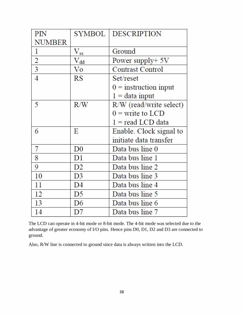
38
The LCD can operate in 4-bit mode or 8-bit mode. The 4-bit mode was selected due to the
advantage of greater economy of I/O pins. Hence pins D0, D1, D2 and D3 are connected to
ground.
Also, R/W line is connected to ground since data is always written into the LCD.

39
Figure 25:Microcontroller-LCD interface simulation
4.1.4 VISUAL ALARM (LEDs)
LEDs were used for the sole purpose of visual alert. One green LED was set to be lit when there
was no significant smoke detected in the environment. In the event that smoke is detected, the
green LED was set to go off. Four red were set to be off when there was no smoke detected and
to blink in the event smoke is detected in the environment.
A current limiting resistance was required for each of the LED. With a Vcc of 5v, the mcu could
give a maximum of 5v while the LED needs 20mA in order to light and a forward voltage of 1.8-
3.3V. From Ohm‟s Law, R=V/I.
R=(VS-Vf)/Is
R=(5-1.8)/(20/1000)=160Ω
In order to ensure the current sourced is as little as possible, 220Ω resistor was chosen for current
limiting, such that the maximum current sourced became;
(5.0V-1.8V)/220Ω=15mA
PB0/T0/XCK1
PB1/T12
PB2/AIN0/INT23
PB3/AIN1/OC04
PB4/SS5
PB5/MOSI6
PB6/MISO7
PB7/SCK8
RESET9
XTAL212
XTAL113
PD0/RXD14
PD1/TXD15
PD2/INT016
PD3/INT117
PD4/OC1B18
PD5/OC1A19
PD6/ICP120
PD7/OC221
PC0/SCL22
PC1/SDA23
PC2/TCK24
PC3/TMS25
PC4/TDO26
PC5/TDI27
PC6/TOSC128
PC7/TOSC229
PA7/ADC733
PA6/ADC634
PA5/ADC535
PA4/ADC436
PA3/ADC337
PA2/ADC238
PA1/ADC139
PA0/ADC040
AREF32
AVCC30
U1
ATMEGA32
D7
14
D6
13
D5
12
D4
11
D3
10
D2
9D
18
D0
7
E6
RW
5R
S4
VS
S1
VD
D2
VE
E3
LCD1LM016L
RV1(2)VALUE=5
RV1
5.0K DESC="TRIMPOT 5.0K OHM 6MM SQ SMD"

40
Figure 26 Microcontroller - LEDs interface simulation
4.1.5 AUDIO ALARM (BUZZER)
A pin type electromagnetic buzzer was selected due to its ease in mounting to printed circuit
board as well as the sound output frequency of 2048Hz which is audible to most people. Its
operating voltage was 3-6v and a maximum current of 60mA.
The buzzer was set to be off when there was no significant amount of smoke detected in the
environment and to be activated when smoke was detected.
It was connected to pin PB0 of the microcontroller.
The final designed circuit was as shown in the next figure:
PB0/T0/XCK1
PB1/T12
PB2/AIN0/INT23
PB3/AIN1/OC04
PB4/SS5
PB5/MOSI6
PB6/MISO7
PB7/SCK8
RESET9
XTAL212
XTAL113
PD0/RXD14
PD1/TXD15
PD2/INT016
PD3/INT117
PD4/OC1B18
PD5/OC1A19
PD6/ICP120
PD7/OC221
PC0/SCL22
PC1/SDA23
PC2/TCK24
PC3/TMS25
PC4/TDO26
PC5/TDI27
PC6/TOSC128
PC7/TOSC229
PA7/ADC733
PA6/ADC634
PA5/ADC535
PA4/ADC436
PA3/ADC337
PA2/ADC238
PA1/ADC139
PA0/ADC040
AREF32
AVCC30
U1
ATMEGA32
D1LED-RED
D2LED-RED
D3LED-RED
D4LED-RED
D5LED-GREEN
R1220
R2220
R3220
R4220
R5220

41
Figure 27 Final design of smoke sensor (Excluding the power supply)
PB0/T0/XCK1
PB1/T12
PB2/AIN0/INT23
PB3/AIN1/OC04
PB4/SS5
PB5/MOSI6
PB6/MISO7
PB7/SCK8
RESET9
XTAL212
XTAL113
PD0/RXD14
PD1/TXD15
PD2/INT016
PD3/INT117
PD4/OC1B18
PD5/OC1A19
PD6/ICP120
PD7/OC221
PC0/SCL22
PC1/SDA23
PC2/TCK24
PC3/TMS25
PC4/TDO26
PC5/TDI27
PC6/TOSC128
PC7/TOSC229
PA7/ADC733
PA6/ADC634
PA5/ADC535
PA4/ADC436
PA3/ADC337
PA2/ADC238
PA1/ADC139
PA0/ADC040
AREF32
AVCC30
U1
ATMEGA32
D7
14D
613
D5
12D
411
D3
10D
29
D1
8D
07
E6
RW
5R
S4
VS
S1
VD
D2
VE
E3
LCD1LM016L
RV1
RV1(2)
U1(AREF)
R110k
R1(2)
R2220
R3220
R4220
R5220
R6220
D1LED-GREEN
D2LED-RED
D3LED-RED
D4LED-RED
D5LED-RED
LS1
BUZZER
J1MQ2 SENSOR

42
4.2 SOFTWARE DESIGN For the microcontroller to interface the sensor and the alarms and the LCD, it had to be
programmed, hence necessitating software design. The following flowchart indicates the
functionality of the circuit and was used as a guide in the software design.
Figure 28 FLOWCHART FOR SOFTWARE DESIGN

43
The software design was divided into the following sections:
ADC program
LCD program
Alarm activation program
Main program
4.2.1 ADC PROGRAM
This was necessitated by the fact that the MQ2 sensor gives an output voltage which is analogous
to the quantity of smoke detected.
The purpose was to convert the analog voltage to a digital number since the microcontroller is
digital.
Atmega 32A has an inbuilt Analog to Digital Converter, with PORTA containing the ADC pins.
The ADC has 10-bit resolution, which implies that there are 2^10=1024 steps. The type of ADC
inside the microcontroller is of successive approximation type.
It has 8 channels, which implies that there are 8ADC pins (PA0…PA7) which are multiplexed
together.
Initializing The ADC program
The ADC Multiplexer Selection Register (ADMUX) has 8 registers.
Registers REFS1 & REFS0 form bits 7 and 6 respectively in ADMUX and are used to choose
the reference voltage. The following combinations maybe used:
REFS1 REFS0 Voltage Reference Selection
0 0 AREF, Internal Vref turned off
0 1 AVCC and AREF pin
1 0 Reserved
1 1 Internal 2.56V Voltage Reference
Since the Vcc (+5v) was to be used as reference, the second option was chosen.
Thus, to initialize ADMUX, the following line of code was written:
ADMUX= (1<<REFS0);
Setting the Prescaler
The ADC Control and Status Register A has the following 8 bits:
Bit 7-ADC Enable (ADEN): Unless it‟s enabled, ADC operations cannot take place across
PORTA.

44
Bit 6-ADC Start Conversion (ADSC): This has to be written to „1‟ before starting any
conversion.
Bit 5-ADC Auto Trigger Enable (ADATE): Setting it to „1‟ enables auto-triggering of
ADC.ADC is triggered automatically at every rising edge of clock pulse.
Bit 4-ADC Interrupt Flag (ADIF): Used to check whether the conversion is complete or not.
Whenever a conversion is finished and the registers are updated, this bit is set to „1‟
automatically.
Bit 3-ADC Interrupt Enable (ADIE): When set to „1‟, the ADC interrupt is enabled.
Bit 2:0-ADC Prescaler Select Bits (ADPS2:0): The prescaler (division factor between the mcu
frequency and ADC frequency) is determined by selecting the proper combination from the
following.
ADPS2 ADPS1 ADPS0 Division Factor
0 0 0 2
0 0 1 2
0 1 0 4
0 1 1 8
1 0 0 16
1 0 1 32
1 1 0 64
1 1 1 128
A prescaler of 8 was chosen. Thus, F_ADC=1M/8=125 kHz
Hence, ADCSRA was initialized as follows:
ADCSRA = (1<<ADEN)|(1<<ADPS1)|(1<<ADPS0);
Reading ADC value
uint16_t adc_read(uint8_t ch) // select the corresponding channel 0~7 // ANDing with ’7? will always keep the value // of ‘ch’ between 0 and 7 ch &= 0b00000111; // AND operation with 7 ADMUX = (ADMUX & 0xF8)|ch; // clears the bottom 3 bits before ORing // start single conversion // write ’1? to ADSC ADCSRA |= (1<<ADSC); // wait for conversion to complete // ADSC becomes ’0? again // till then, run loop continuously while(ADCSRA & (1<<ADSC)); return (ADC);

45
4.2.2 LCD PROGRAM
The LCD was implemented in the 4-bit mode as opposed to the 8-bit mode. In this method, we
are splitting Bytes of data in Nibbles. The advantage of using the 4-bit mode is the utilization of
fewer pins for interfacing with the microcontroller. However, in the 4-bit mode, data must be
sent one nibble at a time, so execution time is twice that of 8-bit mode.
Displaying data using a 4-bit interface consists of sending the high-order nibble followed by the
lower-order nibble through the LCD 4-high-order-data lines. The pulsing of the E-line follows
the last nibble sent. Software must provide a way of reading and writing to the appropriate port
lines, the ones used in data transfer, without altering the value stored in the port bits dedicated to
other uses.
The R/W pin is always low since data is always written into the LCD. The RS pin was connected
to PD0 and was used to control the instructions or characters sent to the LCD. The Enable pin
was connected to PD1 and it was used to enable the LCD to either feed instruction into the
register or write character into it.
4.2.3 ALARM ACTIVATION PROGRAM
When the smoke detected exceeds the rated value, the buzzer is activated, the green LED is
switched off and the red LEDs are switched on in addition to the status indication of „smoke
detected‟ on the LCD. As long as the circuit is powered, the sensor keeps checking for the
presence of smoke.
For the purpose of demonstration, the preset value was 3800 particles per million (ppm).
The following section of the code was responsible for alarm activation:
if(adc_result0>380) PORTB = 0x01;//simultaneously switching on the buzzer and green LED off. PORTB ^= (1<<1);//Blinking the four red LEDs. PORTB ^= (1<<2); PORTB ^= (1<<3); PORTB ^= (1<<4); _delay_ms(1); PORTB ^= (1<<1); PORTB ^= (1<<2); PORTB ^= (1<<3); PORTB ^= (1<<4);
else PORTB &=~(1<<1);//Switching off the red LEDs PORTB &=~(1<<2); PORTB &=~(1<<3); PORTB &=~(1<<4); PORTB = 0x20;//Switching on the green LEDs and switching off the buzzer

46
4.3 PCB DESIGN The circuit was first tested on a breadboard and found to be functioning and the next step was
fabrication. This was to facilitate to fit the whole design on a small board and in a compact
manner. It also helps in improving the organization of the whole design as well make it neat and
presentable.
The first step involved drawing the whole layout on proteus software to determine how the
components will be arranged on the board before replicating the same on the PCB.
The layout of copper wires was drawn on express PCB.
The drawing was then printed on a transparent paper, before the paper was laid on the PCB board
and UV lights passed on them. The copper lines soften the material except the copper lines.
It was then passed through a developing solution of Sodium Hydroxide where only the needed
copper lines were outlined.
The next step involved the ectching process where the weakened copper was removed from the
board, leaving only the needed copper lines.
The final step involved drilling of holes for the needed components, and soldering of
components onto the board.

47
CHAPTER 5: RESULTS
5.1 SIMULATED RESULTS The following results have been obtained after simulation on Proteus software. Since the smoke
sensor gives an output of analog voltage, it was simulated by giving a corresponding voltage to
the input of the microcontroller which was to be connected to the sensor.
Sensor
output
Equivalent
smoke
quantity
State of
GREEN
LED
State of
RED
LED
State
of
buzzer
LCD display
0.00V 0ppm ON OFF OFF STANDBY MODE
QTY=0ppm
0.50V 1020ppm ON OFF OFF STANDBY MODE
QTY=1020ppm
1.00V 2050ppm ON OFF OFF STANDBY MODE
QTY=2050ppm
1.50V 3070ppm ON OFF OFF STANDBY MODE
QTY=3070ppm
1.70V 3480ppm ON OFF OFF STANDBY MODE
QTY=3480ppm
1.80V 3690ppm ON OFF OFF STANDBY MODE
QTY=3690ppm
1.84V 3770ppm ON OFF OFF STANDBY MODE
QTY=3770ppm
1.86V 3810ppm OFF Flashing ON SMOKE DETECTED
QTY=3810ppm
1.90V 3890ppm OFF Flashing ON SMOKE DETECTED
QTY=3890ppm
2.00V 4100ppm OFF Flashing ON SMOKE DETECTED
QTY=4100ppm
2.50V 5120ppm OFF Flashing ON SMOKE DETECTED
QTY=5120ppm
3.00V 6140ppm OFF Flashing ON SMOKE DETECTED
QTY=6140ppm
3.50V 7170ppm OFF Flashing ON SMOKE DETECTED
QTY=7170ppm
4.00V 8190ppm OFF Flashing ON SMOKE DETECTED
QTY=8190ppm
4.50V 9220ppm OFF Flashing ON SMOKE DETECTED
QTY=9220ppm

48
Figure 29 :LCD DISPLAY IN SMOKE DETECTED MODE SIMULATION
D7
14
D6
13
D5
12
D4
11
D3
10
D2
9D
18
D0
7
E6
RW
5R
S4
VS
S1
VD
D2
VE
E3
LCD1LM016L
RV1
RV1(2)

49
Figure 30: LCD DISPLAY IN STANDBY MODE SIMULATION
The critical value for smoke detection was 3800ppm. It was a preset value and could be altered
in the code.
From the simulated results, it was observed that the immediately the smoke quantity was greater
than the pre-set value of 3800ppm, the audio and visual alarms were triggered accordingly.
From the observations, the system achieves the functionality of a smoke detector device.
D7
14D
613
D5
12D
411
D3
10D
29
D1
8D
07
E6
RW
5R
S4
VS
S1
VD
D2
VE
E3
LCD1LM016L
RV1
RV1(2)

50
5.3 RESULTS AFTER IMPLEMENTATION
Figure 31Final Circuit with power switched off
The above diagram shows the final circuit after fabrication, but with the power supply switched
off. As expected, all the LEDs, buzzer and LCD were off regardless of the environmental smoke
conditions.

51
Figure 32 Circuit on breadboard with INSIGNIFICANT quantity of smoke detected
The above image was taken while the circuit was being tested while mounted on a breadboard.
The preset critical value was 3800ppm but the smoke detected was 3770ppm hence it had not
met the threshold for triggering an alarm. The buzzer and red LEDs were off, while the green
LED was on, as expected. The LCD display indicated „standby mode‟, which was an indicator of
insignificant quantity of smoke.

52
Figure 33Final Circuit with INSIGNIFICANT quantity of smoke detected
The above image was taken after fabrication. The preset critical value was 3800ppm but the
smoke detected was 1230ppm hence it had not met the threshold for triggering an alarm. The
buzzer and red LEDs were off, while the green LED was on, as expected. The LCD display
indicated „standby mode‟, which was an indicator of insignificant quantity of smoke.

53
Figure 34 Circuit on Breadboard with SIGNIFICANT quantity of smoke detected
The above image was taken while the circuit was being tested on the breadboard and in a smoky
environment. The red LEDs were blinking, the buzzer was activated and the LCD display
indicated „SMOKE DETECTED‟ and a quantity of 4810ppm. This was as expected since the
quantity of smoke had surpassed the preset value of 3800ppm.

54
Figure 35 Final Circuit with SIGNIFICANT quantity of Smoke Detected
The above image was taken after the circuit was fabricated and in a smoky environment. The red
LEDs were blinking, the green LED was off, the buzzer was activated and the LCD display
indicated „SMOKE DETECTED‟ and a quantity of 5390ppm. This was as expected since the
quantity of smoke had surpassed the preset value of 3800ppm.
All the aforementioned observations were in accordance with the design specifications for the
project. The only major limitation while taking the observations is the positioning of the sensor
and the direction of the wind since detection would not occur unless the MQ2 sensor comes
directly in contact with the smoke particles.
The LCD display also indicates the quantity of smoke upto 10000ppm, since that is the only
range within which the sensor operates linearly.

55
CHAPTER 6: CONCLUSION AND RECOMMENDATION
6.1 CONCLUSION The main objective of this project has been to design a circuit that detects smoke and
consequently triggers an alarm. This objective was met since the systems works effectively.
As the smoke detected in the environment varied, the LCD displayed the quantity constantly in
particles per million (ppm).
With the smoke below the preset critical value, the green LED was on and the red LEDs were off
and the LCD displayed „STANDBY MODE‟. With the smoke detected above the preset critical
value, the green LED was off while the red LEDs were flashing and the LCD displayed
„SMOKE DETECTED‟.
This system can be of great in domestic as well as industrial settings to detect smoke and alert
people on an impending fire since smoke is a precursor for fire, instead of relying on
heat/temperature sensors which sounds alarm when the fire has already started. This can go a
long way in helping to save human life. This system can also be used to detect and deter smokers
in areas where smoking is prohibited.
The cost of implementing this system is relatively low since the components used are relatively
cheap and are easily available in the market. The single microcontroller can be used to interface
several sensors with alarms located in different locations as long as more pins are freed for
multiple inputs multiple outputs.
This system comes with a power supply that can be directly plugged to the mains (240V AC)
source and give the appropriate operating voltage.

56
6.2 RECOMMENDATIONS Human safety is a very crucial aspect in both domestic and industrial setting, hence use of smoke
sensors is inevitable in addition to other more sophisticated security systems.
This system should be placed in a cool and dry place in order to ensure a longer life span. It
should also be placed in a high place in the room and in the direction of the window where there
is most likely to be the direction of the wind to facilitate the contact of the sensor with the
smoke. The visual alarms should be positioned a few meters above the ground on an easily
visible place. The audio alarm should be as well positioned in a place that its alarm can be easily
heard.
Lastly, the method of relaying the alarm remotely has not been explored in this project due to
time constraint. GSM and GPS modules can be employed in this case to automatically send a
message to a control room to notify operator on the presence of smoke and the exact location of
smoke.

57
References
[1] "https://en.m.wikipedia.org/wiki/Smoke_detector," [Online].
[2] J. Milke, "History of Smoke Detection: A profile of how the technology and role of smoke detection
has changed".
[3] "www.madehow.com/Volume-2/Smoke-Detector.html," [Online].
[4] "www.electroschematics.com," [Online].
[5] Microchip, "RE46C190 Demo Board Users' Guide".
[6] "183474-da-01-en-Gassensor_TGS_813".
[7] Hanwei Electronics Co LTD, "http://www.hwsensor.com," [Online].
[8] Atmel, Atmega 32A Datasheeet.
[9] "Liquid-Crystal Display Wikipedia," [Online].
[10] Fujitsu Microelectronics America Inc, "Fundamentals of Liquid Crystal Display - How They Work and
What They Do".
[11] "Light-emmiting Diode - Wikipedia," [Online].
[12] "jenswilly.dk/tag/photointerrupter/," [Online].
[13] "www.microchip.com," [Online].
[14] "https://electrosome.com/power-supply-design-5v-7805-voltage-regulator/," [Online].
[15] "maxembedded.com/2011/06/the-adc-of-the-avr/," [Online].
[16] E. Hughes, Hughes Electrical and Electronic Technology, Essex: Pearson Education Limited, 2008.
[17] J. Bird, Electrical & Electronic Principles, Oxford: Newnes, 2010.
[18] J. Bird, Electrical Circuit Theory & Technology, Oxford: Newnes, 2003.

58
[19] C. K. A. &. M. N. Sadiku, Fundamentals of Electrical Circuits.
[20] I. S. &. J. Dunton, Practical Electronics Handbook, Oxford, 2007.
APPENDIX 1: CIRCUIT DIAGRAM
PB0/T0/XCK1
PB1/T12
PB2/AIN0/INT23
PB3/AIN1/OC04
PB4/SS5
PB5/MOSI6
PB6/MISO7
PB7/SCK8
RESET9
XTAL212
XTAL113
PD0/RXD14
PD1/TXD15
PD2/INT016
PD3/INT117
PD4/OC1B18
PD5/OC1A19
PD6/ICP120
PD7/OC221
PC0/SCL22
PC1/SDA23
PC2/TCK24
PC3/TMS25
PC4/TDO26
PC5/TDI27
PC6/TOSC128
PC7/TOSC229
PA7/ADC733
PA6/ADC634
PA5/ADC535
PA4/ADC436
PA3/ADC337
PA2/ADC238
PA1/ADC139
PA0/ADC040
AREF32
AVCC30
U1
ATMEGA32
D7
14
D6
13
D5
12
D4
11
D3
10
D2
9D
18
D0
7
E6
RW
5R
S4
VS
S1
VD
D2
VE
E3
LCD1LM016L
RV1
RV1(2)
U1(AREF)
R110k
R1(2)
R2220
R3220
R4220
R5220
R6220
D1LED-GREEN
D2LED-RED
D3LED-RED
D4LED-RED
D5LED-RED
LS1
BUZZER
J1MQ2 SENSOR

59
TRANSFORMER
TRAN-2P3S
D1
1N4007
D2
1N4007
C16800u
C20.33u
C30.1u
VI1
VO3
GN
D2
U1REG-POS

60
APPENDIX 2: ATMEGA 32A BLOCK DIAGRAM

61
APPENDIX 3: C PROGRAM /* * * * Created: 3/29/2016 12:25:41 PM * Author: NG'ANG'A RENSON NGOCHI F17/1421/2011 */ /*PROJECT 107-SMOKE DETECTOR * * */ #ifndef F_CPU #define F_CPU 1000000UL // 1 MHz clock speed #endif #define D4 eS_PORTD4 #define D5 eS_PORTD5 #define D6 eS_PORTD6 #define D7 eS_PORTD7 #define RS eS_PORTD0 #define EN eS_PORTD1 #include <avr/io.h> #include <util/delay.h> #include "lcd.h" uint16_t adc_result0; void adc_init() // AREF = AVcc ADMUX = (1<<REFS0); // ADC Enable and prescaler of 8 // 1000000/8 = 125000. ADCSRA = (1<<ADEN)|(1<<ADPS1)|(1<<ADPS0); uint16_t adc_read(uint8_t ch) // select the corresponding channel 0~7 // ANDing with ’7? will always keep the value // of ‘ch’ between 0 and 7 ch &= 0b00000111; // AND operation with 7 ADMUX = (ADMUX & 0xF8)|ch; // clears the bottom 3 bits before ORing // start single conversion // write ’1? to ADSC ADCSRA |= (1<<ADSC); // wait for conversion to complete // ADSC becomes ’0? again // till then, run loop continuously while(ADCSRA & (1<<ADSC)); return (ADC); int main(void) MCUCSR=(1<<JTD);

62
MCUCSR=(1<<JTD);//temporarily disabling JTAG _delay_ms(10); DDRD = 0xFF; DDRA = 0x00; DDRC = 0xFF; DDRB = 0x3F; PORTB &=~(1<<1); PORTB &=~(1<<2); PORTB &=~(1<<3); PORTB &=~(1<<4); PORTB &=~(1<<5); Lcd_Init(); adc_init(); Lcd_Set_Cursor(1,1); Lcd_Write_String(" WELCOME"); _delay_ms(200); Lcd_Clear(); Lcd_Set_Cursor(1,1); Lcd_Write_String("RENSON PROJECT"); Lcd_Set_Cursor(2,1); Lcd_Write_String("F17/1421/2011"); _delay_ms(200); Lcd_Clear(); while(1) adc_result0 = adc_read(0); // read adc value at PA0 char display[20] = "QTY= "; char countstr[6]; snprintf(countstr,6,"%d",adc_result0*10); strcat(display,countstr); strcat(display," ppm"); if(adc_result0>380) PORTB = 0x01;//simultaneously switching on the buzzer and green LED off. PORTB ^= (1<<1);//Blinking the four red LEDs. PORTB ^= (1<<2); PORTB ^= (1<<3); PORTB ^= (1<<4); _delay_ms(1); PORTB ^= (1<<1);

63
PORTB ^= (1<<2); PORTB ^= (1<<3); PORTB ^= (1<<4); Lcd_Set_Cursor(1,1); Lcd_Write_String("SMOKE DETECTED"); Lcd_Set_Cursor(2,1); Lcd_Write_String(display); else PORTB &=~(1<<1);//Switching off the red LEDs PORTB &=~(1<<2); PORTB &=~(1<<3); PORTB &=~(1<<4); PORTB = 0x20;//Switching on the green LEDs and switching off the buzzer Lcd_Set_Cursor(1,1); Lcd_Write_String("STANDBY MODE "); Lcd_Set_Cursor(2,1); strcat(display," "); Lcd_Write_String(display);

64
APPENDIX 4: COST Component Quantity Unit
Cost(KSh)
Total
Cost(KSh)
MQ2 sensor 1 700 700
Atmega 32A 1 450 450
LCD 1 400 400
Buzzer 1 30 30
LED 5 5 25
Resistor 7 3 21
Potentiometer 1 20 20
Switches 3 20 60
PCB board 1 600 600
Transformer 1 450 450
Diode 2 10 20
Electrolytic
capacitor
2 10 20
Polyster capacitors 2 5 10
Voltage regulator
(LM 7805)
1 50 50
Breadboard 1 250 250
Connecting Wires - 200 200
TOTAL COST 3306

65