university of nairobieie.uonbi.ac.ke/sites/default/files/cae/engineering/eie/an... · electronics...
TRANSCRIPT

UNIVERSITY OF NAIROBI
FACULTY OF ENGINEERING
DEPARTMENT OF ELECTRICAL AND ELECTRONIC ENGINEERING
FINAL YEAR PROJECT
TIITLE: AN ELECTRICAL POWER SUPPLY QUALITY MONITOR
PROJECT NO. 48
AUTHOR: ODHIAMBO K. O
REG.NO. F17/2141/2004
SUPERVISOR: PROF. ELIJAH MWANGI
EXAMINER: DR. MBUTHIA
DATE: MAY 2009
Submitted to the department of electrical and electronic engineering in partial fulfillment for the award of a degree in Bachelor of Science in Electrical and Electronic Engineering.

PROJECT NO: 48
TITTLE: ELECTRICAL POWER SUPPLY QUALITY
MONITOR.
BY: ODHIAMBO K.O
F17/2141/2004
SUPERVISOR: PROF.ELIJAH MWANGI
This project has been submitted in partial fulfillment of the
requirements for the Bachelor of Science degree in Electrical and
Electronics Engineering of the University of Nairobi.
May, 2009

Dedication
To my parents, brothers and sisters and Keren for the shoulders to always lean on.

ACKNOWLEDGEMENT
I would like to take this opportunity to thank all who contributed to this project through technical
guidance and moral support.
I would like to particularly thank my supervisor Professor Elijah Mwangi for his guidance on the
entire project approach.
Finally I would like to appreciate all members of the class of 2009 for their support.

ABSTRACT
The project is an electrical power supply quality monitor which examines the quality of the
mains supply voltage and frequency.
The project uses analogue devices which includes diodes, op-amps and mos-fet to monitor
frequency and voltage being supplied from the available mains. This translates to three sections;
the frequency monitoring section, the voltage monitoring section and the spikes and noise
detection section.
The objective being to design a cheap power supply quality monitor, the project was designed
and simulated according to the specifications with results achieved.

TABLE OF CONTENTS
1. CHAPTER ONE : INTRODUCTION----------------------------------------------1
2. CHAPTER TWO: LITERATURE REVIEW------------------------------------2
2.1 Power quality ------------------------------------------------------------------------2
2.1.1 Voltage dips---------------------------------------------------------------------2
2.1.2 Voltage Surges/Spikes---------------------------------------------------------5
2.1.3 Overvoltages--------------------------------------------------------------------6
2.1.4 Harmonics-----------------------------------------------------------------------6
2.1.5 Frequency Variations----------------------------------------------------------7
2.1.6 Voltage Fluctuations-----------------------------------------------------------7
2.1.7 Voltage Unbalance-------------------------------------------------------------7
2.1.8 Supply Interruptions-----------------------------------------------------------8
2.1.9 Undervoltage--------------------------------------------------------------------8
2.1.10 Transients----------------------------------------------------------------------8
2.1.11 Rapid voltage change---------------------------------------------------------9
2.2 Power Quality monitoring---------------------------------------------------------9
2.3 Types of Installation----------------------------------------------------------------9
2.4 Improving power quality----------------------------------------------------------9
2.5 Voltage Monitor-------------------------------------------------------------------10
3.0 CHAPTER THREE: DESIGN------------------------------------------------------12
3.1 Noise and Spikes Detector-------------------------------------------------------13
3.2 Frequency Detector---------------------------------------------------------------14
3.3 Overvoltage circuit----------------------------------------------------------------15
3.3.1 Rectification---------------------------------------------------------------------16

3.3.2 The transformer--------------------------------------------------------------19
3.3.3 Construction features--------------------------------------------------------20
3.3.4 Principle of operation--------------------------------------------------------20
3.3.5 Transformer connection-----------------------------------------------------20
3.3.6 E.M.F Equation---------------------------------------------------------------21
3.3.7 The 741 Operational Amplifier---------------------------------------------22
3.3.8 metal-oxide-semiconductor FET-------------------------------------------23
3.3.8.1 Circuit symbols-------------------------------------------------------------24
3.3.8.2 MOSFET operation--------------------------------------------------------25
3.3.8.3 Modes of operation---------------------------------------------------------26
4.0 Principle of operation-------------------------------------------------------------28
5.0 Design simulation and results---------------------------------------------------29
6.0 Conclusion and Recommendation----------------------------------------------37
REFERENCE

1. INTRODUCTION
An electrical power supply quality monitor is a device which examines the status of the mains
electrical parameters that is the frequency and the voltage.
This project objectively entails the design and simulation of a mains power supply quality
monitor. The distinctive objective of the design being to lower the cost of a power quality
monitor by using cheaply available analogue devices to design one.
The design task is to simulate a real time quality monitor that can be directly connected to the
mains or interfaced with digital devices for improved monitoring. The measured parameters are
to be obtained from the various parts of the design which includes: spikes and noise detection
circuit, voltage detection circuit and the frequency monitoring section.
For visual indications the design made use of cheap LEDs and for audio indications the use of a
speaker and a buzzer was employed.
Finally, to aid observation oscilloscope and digital multi-meter were used to ascertain the
simulated results.
2.0 LITERATURE REVIEW
2.1 Power quality
`Power quality’ is the absence of various kinds of disturbances on single-phase low voltage ac
supply mains. Such disturbances include transient overvoltages from lighting and switching
reactive loads, large departures from nominal root mean square voltage, severe harmonic
distortion, and outages. Disturbances on the ac supply mains can cause electronic circuits and
systems to malfunction or even be damaged. A disturbance that affects a process control
computer in a large industrial complex could easily result in shutdown of the process. The lost
production and product loss or recycling during start-up represents a large cost to the business.
Similarly, a protection relay affected by a disturbance though conduction or radiation from
nearby conductors could trip a feeder or substation, causing loss of supply to a large number of
consumers. At the other end of the scale, a domestic user of a PC has to re-boot the PC due to a
transient voltage dip, causing annoyance to that and other similarly affected users. The
disturbances may come in the following forms:
• Large magnitude like transient overvoltage and surge
• Sudden decrease in magnitude as in the case of a notch
• Severe harmonic distortion
• Sudden loss of useful power caused by severe sag or beginning of outage
• High frequency noise
• Changes in frequency of mains voltage
• Unacceptable value of root mean square voltage like sag or swell.
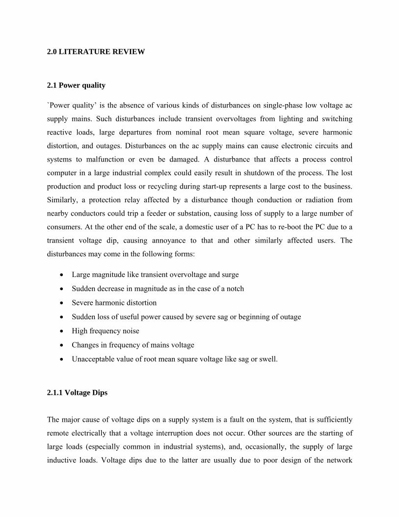
2.1.1 Voltage Dips
The major cause of voltage dips on a supply system is a fault on the system, that is sufficiently
remote electrically that a voltage interruption does not occur. Other sources are the starting of
large loads (especially common in industrial systems), and, occasionally, the supply of large
inductive loads. Voltage dips due to the latter are usually due to poor design of the network

feeding the consumer. A voltage dip is the most common supply disturbance causing interruption
of production in an industrial plant. Faults on a supply network will always occur, and in
industrial systems, it is often practice to specify equipment to ride-through voltage dips of up to
0.2s. The most common exception is contactors, which may well drop out if the voltage dips
below 80% of rated voltage for more than 50-100ms. Motor protection relays that have an under
voltage element setting that is too sensitive is another cause. Since contactors are commonly
used in circuits supplying motors, the impact of voltage dips on motor drives, and hence the
process concerned, requires consideration. Other network-related fault causes are weather–
related (such as snow, ice, wind, salt spray, dust) causing insulator flashover, collisions due to
birds, and excavations damaging cables. Multiple voltage dips, as illustrated in Figure 23.3,
cause more problems for equipment than a single isolated dip. The impact on consumers may
range from the annoying (non-periodic light flicker) to the serious (tripping of sensitive loads
and stalling of motors). Where repeated dips occur over a period of several hours, the repeated
shutdowns of equipment can give rise to serious production problems. Figure 23.4 shows an
actual voltage dip, as captured by a Power Quality recorder. Typical data for under voltage
disturbances on power systems during evolving faults are shown in Figure23.5.
Disturbances that lie in the front right-hand portion of the histogram are the ones that cause most
problems, but fortunately these are quite rare.
Fig 2.1 Voltage dip profile
Vrms Nominal high
Nominal low
Interruption
Time
Dip duration
Percentage below nominal Retained voltage
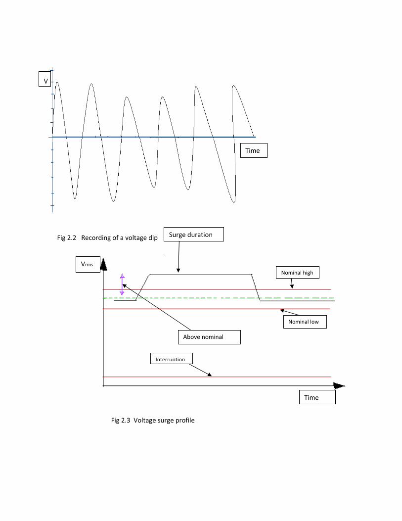
Fig 2.2 Recording of a voltage dip
Fig 2.3 Voltage surge profile
V
Time
Vrms
Time
Surge duration
Above nominal
Nominal high
Nominal low
Interruption

Fig 2.4 Supply waveform distorted due to presence of harmonics
2.1.2 Voltage Surges/Spikes
Voltage surges/spikes are the opposite of dips – a rise that may be nearly instantaneous (spike) or
takes place over a longer duration (surge). These are most often caused by lightning strikes and
arcing during switching operations on circuit breakers/contactors (fault clearance, circuit
switching, especially switch-off of inductive loads). Figure 2.3 shows the profile of a voltage
surge. Equipment may suffer serious damage from these causes, ranging from insulation damage
to destruction of sensitive electronic devices. The damage may be immediate and obvious by the
fact that equipment stops working, through to failure at a much later date from deterioration
initiated from a surge or spike of voltage. These latter failures are very difficult to distinguish
from random failures due to age, minor manufacturing defects, etc.
Time
V
2.1.3 Overvoltages
Sustained overvoltages are not common. The most likely causes are maladjusted voltage
regulators on generators or on-load tap changers, or incorrectly set taps on fixedtap transformers.
Equipment failures may immediately result in the case of severe overvoltages, but more likely is
accelerated degradation leading to premature failure without obvious cause. Some equipment
that is particularly sensitive to overvoltages may have to be shut down by protective devices.
2.1.4 Harmonics
This is a very common problem in the field of Power Quality. The main causes are Power
Electronic Devices, such as rectifiers, inverters, UPS systems, static var compensators, etc. Other
sources are electric discharge lamps, arc furnaces and arc welders. In fact, any nonlinear load
will be a source of harmonics. Figure 23.7 illustrates a supply waveform that is distorted due to
the presence of harmonics. Harmonics usually lead to heating in rotating equipment (generators
and motors), and transformers, leading to possible shutdown. Capacitors may be similarly
affected. If harmonic levels are sufficiently high enough, protective devices may shut the
equipment down to avoid damage. Some equipment, such as certain protection devices, may mal
operate and cause unnecessary shutdowns. Special provision may have to be made to filter
harmonics from the measured signals in these circumstances. Interference may be caused to
communication systems. Overloading of neutral conductors in LV systems has also occurred (the
harmonics in each phase summing in the neutral conductor, not cancelling) leading to failure due
to overheating. This is a particular risk in buildings that have a large number of PC’s, etc., and in
such cases a neutral conductor rated at up to 150% of the phase conductors has been known to be
required. Bus bar risers in buildings are also at risk, due to harmonic-induced vibration causing
joint securing bolts, etc. to work loose.
2.1.5 Frequency Variations
Frequency variations that are large enough to cause problems are most often encountered in
small isolated networks, due to faulty or maladjusted governors. Other causes are serious
overloads on a network, or governor failures, though on an interconnected network, a single
governor failure will not cause widespread disturbances of this nature. Network overloads are
most common in areas with a developing electrical infrastructure, where a reduction in frequency
may be a deliberate policy to alleviate overloading. Serious network faults leading to islanding of
part of an interconnected network can also lead to frequency problems. Few problems are
normally caused by this problem. Processes where product quality depends on motor speed
control may be at risk but such processes will normally have closed-loop speed controllers.
Motor drives will suffer output changes, but process control mechanisms will normally take care
of this. Extreme under- or over frequency may require the tripping of generators, leading to the
possibility of progressive network collapse through network overloading/under frequency causes.
2.1.6 Voltage Fluctuations
These are mainly caused by load variations, especially large rapid ones such as are likely to
occur in arc and induction heating furnaces, rolling mills, mine winders, and resistance welders.
Flicker in incandescent lamps is the most usual effect of voltage fluctuations. It is a serious
problem, with the human eye being particularly sensitive to light flicker in the frequency range
of 5-15Hz. Because of the wide use of such lamps, the effects are widespread and inevitably give
rise to a large number of complaints. Fluorescent lamps are also affected, though to a lesser
extent.
2.1.7 Voltage Unbalance
Unbalanced loading of the network normally causes voltage unbalance. However, parts of the
supply network with unbalanced impedances (such as untransposed overhead transmission lines)
will also cause voltage unbalance, though the effect of this is normally small. Overheating of
rotating equipment results from voltage unbalance. In serious cases, tripping of the equipment
occurs to protect it from damage, leading to generation/load imbalance or loss of production.
2.1.8 Supply Interruptions
Faults on the power system are the most common cause, irrespective of duration. Other causes
are failures in equipment, and control and protection malfunctions. Electrical equipment ceases
to function under such conditions, with undervoltage protection devices leading to tripping of
some loads. Short interruptions may be no more than an inconvenience to some consumers (e.g.
domestic consumers), but for commercial and industrial consumers (e.g. semiconductor
manufacture) may lead to lengthy serious production losses with large financial impact. Longer
interruptions will cause production loss in most industries, as induction and synchronous motors
cannot tolerate more than 1-2 seconds interruption without having to be tripped, if only to
prevent excessive current surges and resulting large voltage dips on supply restoration. On the
other hand, vital computer systems are often fed via a UPS supply that may be capable of
supplying power from batteries for several hours in the event of a mains supply failure. More
modern devices such as Dynamic Voltage Restorers can also be used to provide continuity of
supply due to a supply interruption. For interruptions lasting some time, a standby generator can
be provide a limited supply to essential loads, but cannot be started in time to prevent an
interruption occurring.
2.1.9 Undervoltage
Excessive network loading, loss of generation, incorrectly set transformer taps and voltage
regulator malfunctions, cause undervoltage. Loads with a poor power factor (see Chapter 18 for
Power Factor Correction) or a general lack of reactive power support on a network also
contribute. The location of power factor correction devices is often important, incorrect location
resulting in little or no improvement. The symptoms of undervoltage problems are tripping of
equipment through undervoltage trips. Lighting will run at reduced output. Undervoltage can
also indirectly lead to overloading problems as equipment takes an increased current to maintain
power output (e.g. motor loads). Such loads may then trip on overcurrent or thermal protection.
2.1.10 Transients
Transients on the supply network are due to faults, control and protection malfunctions, lightning
strikes, etc. Voltage-sensitive devices and insulation of electrical equipment may be damaged, as

noted above for voltage surges/spikes. Control systems may reset. Semiconductor manufacture
can be seriously affected unless the supplies to critical process plant are suitably protected.
2.1.11 Rapid voltage change
Rapid voltage change is caused by motor starting and transformer tap changing. In this case
undesired effects may be felt in the form of overheating in motors and generators and
interruption of three phase operation.
2.2 POWER QUALITY MONITORING
If an installation or network is thought to be suffering from problems related to Power Quality,
suitable measurements should to be taken to confirm the initial diagnosis. These measurements
will also help quantify the extent of the problem(s) and provide assistance in determining the
most suitable solutions. Finally, follow up measurements after installation will confirm the
effectiveness of the remedial measures taken.
2.3 Type of Installation
Monitoring equipment for Power Quality may be suitable for either temporary or permanent
installation on a supply network. Permanent installation is most likely to be used by Utilities for
routine monitoring of parts of their networks to ensure that regulatory limits are being complied
with and to monitor general trends in respect of power quality issues. Consumers with sensitive
loads may also install permanent monitoring devices in order to monitor Power Quality and
provide supporting evidence in the event of a claim for compensation being made against the
supplier if loss occurs due to a power quality problem whose source is in the Utility network.
2.4 Improving power quality
There are many ways to reduce the effects of poor power quality, and it is important to select an
appropriate solution with an adequate rating.
• Constant voltage transformers (CVTs) use saturation of transformer core to provide
output voltage regulation. The regulation is automatic, with no electronic circuitry and
moving parts.
• Automatic voltage stabilizers (AVS) use a transformer to add or subtract a small
percentage to the incoming voltage. Microprocessor control monitors the incoming mains
supply, and electronically selects a transformer tap so that output voltage stays close to
nominal.
• Regulators are electro-mechanical devices, consisting of a variable transformer (variac)
driven by a motor to adjust the output voltage close to the required level.
• Conditioner is a term usually applied to the device that regulate the voltage against input
voltage variations and absorbs surges and transients. They are effectively a stabilizer or
regulator, with added surge suppression and filtering functions.
• Passive harmonic filters consist of an array of passive components (capacitors, inductors
and resistors), designed to absorb harmonic currents. They are generally applied at larger
installations and require careful design, depending on measurements of voltage distortion.
• Power electronic compensators perform a similar function to passive filters, but they can
self-adapt to changing conditions and are much more controllable. In case of an overload
they will provide all the compensation they can within their rating, where a passive filter
may trip or fail.
• Surge suppressors are devices that conduct little until a threshold voltage is exceeded,
when they conduct and absorb energy to limit the voltage. They are available in sizes
from those to protect a single appliance, to those for high voltage electrical distribution.
Devices are available that combine suppresors with passive filtering for a single device or
group. Self-monitoring model that indicates continuing protection is preferable as
repeated operation or transients of too high a level can cause failure.
2.5 Voltage Monitor
Voltage monitoring circuits report when a voltage is beyond one or more pre-defined limits.
These circuits are used for many purposes, ranging from determining when a power supply has
achieved stable operation to determining when a sensed variable in a manufacturing process has
drifted out of tolerance. Although it is possible to monitor a voltage with an analog-to-digital
converter and make an in-bounds/out-of-bounds determination digitally with a microprocessor, a
completely analog solution is often simpler to implement or offers performance advantages such
as fast reaction time.

The design is also done by use of readily available and easy to use components such as diodes,
capacitors, op amps and resistors. Any complexity may be seen in the choice of transformer
which is relatively simpler in comparison to the use of a microprocessor.

3.0 DESIGN
The design approach employed voltage and frequency monitoring. The design consists of an
overvoltage detector, noise and spikes sensor and frequency detector.
Fig 3.1 Block diagram of the system design
This consists of:
• Noise and spike section
• Frequency monitor section
• Rectification and smoothening
• Overvoltage and undervoltage circuit
The noise and spikes section is responsible for detecting the presence of noise the mains.
Frequency monitor section is in charge of evaluating over and under frequency against the set
frequencies. This has a step down transformer which is connected to the overvoltage circuit. It
supplies the voltage to this circuit. The construction of the circuit is described in the section that
follows.
NOISE AND SPIKES SECTION
FREQUENCY DISTURBANCE DETECTOR
RECTIFICATION AND SMOOTHENING
OVER VOLTAGE AND UNDERVOLTAGE CIRCUIT
AC

3.1 Noise and spikes detector
Fig 3.2 Noise and spikes detector circuit
The noise section consists of a 50 hertz filter, a speaker and a bicolor light emitting diode.
The filter works to eliminate the spikes and allows for the detection of noise. The filter has three
400V 470 nano farads capacitors, two in parallel which in turn are in series with the other
capacitor. It also has a 2 watts 47 kilo ohms resistor in series with the two capacitors in parallel.
The bicolor light emitting diode gives the visual indication of noise or asymmetry in the wave.
The noise overimposed in the pure sinusoidal wave is visibly indicated by this set-up. The 5 kilo
ohms potentiometer is adjusted to allow for the least light from the light emitting diodes. In this
case it is possible to vary the sensitivity of the noise detection.
The 8 ohms speaker is connected through an audio transformer. This gives an audio indication of
noise.
The spike detector circuit has a constituent of a silicon controlled rectifier, a potentiometer and a
buzzer. By controlling the gate current through the SCR the buzzer is able to give a spike
presence indication.
C1470nF
R13.3kΩ
C2
470nF
C3470nF
R2
47kΩ
R3
5kΩKey=A 50%
LED1
LED2
R4270Ω
D1
1N4948GPD2
1N4948GP
T1
TS_AUDIO_VIRTUAL
XLV1
Input
R5
1kΩKey=A 50%
D31N4007
D5BT145_500R
R65.6kΩ
6
45
120
10
9
8731
D4
1N4007
U1
BUZZER200 Hz
R7
10kΩ C4470nF
1411 13
2
0

3.2 Frequency detector
The main part of this circuit makes use of the rectifying characteristics of the diode.
Fig 3.3 Frequency detector circuit
By setting an optimal range of frequency the behavior of the diode D1 or D3 is monitored. In this
case the full-wave rectification characteristic of the diode is the principle pointer to the frequency
variation from the set value. The values of capacitances and resistors are selected to match this
calibration. When the frequency deviates either below or above the predetermined value the
waveform observed will not be that of fully rectified diode.
The fluctuations in the mains frequency causes motors and generators to run at high or low
synchronous speed. The speed of the synchronous machines is dependent on the frequency of the
supply and the size of the poles of the machine. The speed increases with increase in supply
frequency.
However, in a production industry like the soft drinks industries, vehicle manufacturing
industries, precision is highly valued. In this case any slight variation in the speed of the motors
used to tighten the bottles, move them or even tighten bolts in the case of vehicles will results to
an undesired result. Thus these companies employs a frequency monitoring device to determine
whether it is necessary to put in place frequency stabilizers.
C1
470nF
C2470nF
C3570nF
C4
100uFC5
400nF
C6470nFC7
470nF
R13.9kΩ
R24.02kΩ
R347kΩ
R4
25kΩ
R547kΩ
R62.2kΩ
R73.777kΩ
R83.9kΩ
D1
1N4007
D21N4007
D3
1N4007
D41N4007
25
4
6
7 8 9
10
11
1
0

3.3 Overvoltage circuit
Fig 3.4 Overvoltage circuit
For overvoltage and undervoltage, the configuration in Figure 1b. In this case, it is assumed
|VWIN–|>|VWIN+|, where |VWIN–| is the magnitude of the negative window voltage and |VWIN+| is
the magnitude of the positive window voltage. Q1 is an NMOS enhancement-mode MOSFET
that has a threshold voltage of approximately 1V. The source terminal of Q1 connects to the
negative input of the op amp; thus, it remains at a virtual-ground potential. The gate terminal
connects to the op amp's output, which turns Q1 on whenever the output voltage exceeds Q1's
threshold voltage.
For input voltages greater than 0V, the op amp produces a negative voltage and Q1 turns off. The
ratio of R2 and R1 sets the op-amp gain, and the output clamps at the on-state voltage of the green
LED, approximately –2.1V. For input voltages lower than 0V, Q1 turns on once the op amp's
output exceeds the threshold voltage of Q1. In this case, the ratio of R1 and the parallel
combination of R2 and R3 sets the op-amp gain, and the maximum output voltage is the on-state
U1
741
3
2
4
7
6
51
Q1ZVN4424G
LED1LED2
R1
5kΩ
R2
5kΩ
R3
4.3kΩ
R4
5kΩ
2
3
VCC15V
VEE-15V
VDD-5V
VDD
VCC
VEE
7T20
1
2
3
D4
1N4004
D5
1N4004
D1
1N4004
D2
1N4004
R5
1kΩ
139
0
51
4
0

voltage of the red LED, 2V. Resistor R4 again serves as a current limiter for the LEDs. The
relationship between the resistor values and the positive and negative window voltages is given
by the following equations. For simplicity, the positive magnitude of the voltages was used, and
the difference between the forward voltages of the red and green LEDs was also neglected.
The value of R1 is chosen such that the feedback current through R4 is small in comparison
with the on-state LED current. Choosing R3 is such that its value is much greater than the on-
resistance of Q1.
3.3.1 Rectification
The voltage monitor circuit accepts a dc voltage. This implies that the mains supply voltage must
be rectified before being fed in this system. The rectifier unit converts the a.c voltage from the
step down transformer secondary winding into pulses of unidirectional current. Three types of
rectifier circuit are used for single phase: the half-wave, the full-wave and the bridge rectifier.
The half-wave rectifier although being a simple circuit has the main disadvantage of low
efficiency.

Fig 3.5 Diagram of half wave rectifier
Fig 3.6 Rectifier input and output voltage waveforms.
Vo1
Vd
T1
The diode conducts only during one half of the cycle so the efficiency cannot be greater than
50%
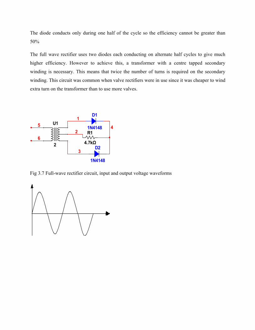
The full wave rectifier uses two diodes each conducting on alternate half cycles to give much
higher efficiency. However to achieve this, a transformer with a centre tapped secondary
winding is necessary. This means that twice the number of turns is required on the secondary
winding. This circuit was common when valve rectifiers were in use since it was cheaper to wind
extra turn on the transformer than to use more valves.
Fig 3.7 Full-wave rectifier circuit, input and output voltage waveforms
U1
2
R1
4.7kΩ
D1
1N4148
D2
1N4148
1
2
3
45
6
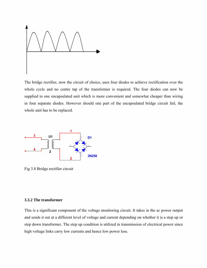
The bridge rectifier, now the circuit of choice, uses four diodes to achieve rectification over the
whole cycle and no centre tap of the transformer is required. The four diodes can now be
supplied in one encapsulated unit which is more convenient and somewhat cheaper than wiring
in four separate diodes. However should one part of the encapsulated bridge circuit fail, the
whole unit has to be replaced.
Fig 3.8 Bridge rectifier circuit
3.3.2 The transformer
This is a significant component of the voltage monitoring circuit. It takes in the ac power output
and sends it out at a different level of voltage and current depending on whether it is a step up or
step down transformer. The step up condition is utilized in transmission of electrical power since
high voltage links carry low currents and hence low power loss.
D1
3N258
1
2
4
3
U1
2
1
2
3
4
3.3.3 Construction features
Transformer consists of two coils which are magnetically coupled (through mutual inductance).
The coils can be wound on a laminated steel core or just air cored. The most commonly used
transformers are sheet-steel laminated and then assembled to provide a continuous magnetic path
with minimum air gaps. The steel used is of high silicon content sometimes heat treated to
produce a high permeability and low hysteresis loss at the usual operating flux densities. The thin
sheets of steel are separated from one another by a thin film of insulation. Such a film can be a
coat of insulating varnish, a sheet of paper pasted on the surface and sometimes even the film of
oxide remaining on the surface. This minimizes the eddy currents loss whose magnitude is
directly proportional to the square of the frequency and the square of the thickness of the
material.
3.3.4 Principle of operation
3.3.5 Transformer connection
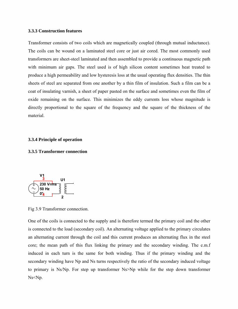
Fig 3.9 Transformer connection.
One of the coils is connected to the supply and is therefore termed the primary coil and the other
is connected to the load (secondary coil). An alternating voltage applied to the primary circulates
an alternating current through the coil and this current produces an alternating flux in the steel
core; the mean path of this flux linking the primary and the secondary winding. The e.m.f
induced in each turn is the same for both winding. Thus if the primary winding and the
secondary winding have Np and Ns turns respectively the ratio of the secondary induced voltage
to primary is Ns/Np. For step up transformer Ns>Np while for the step down transformer
Ns<Np.
U1
2
V1
230 Vrms 50 Hz 0°
3
4

3.3.6 E.M.F EQUATION
Let the flux produced due to the current in the primary be given by
φ=φmsinωt
φm is te peak value of magnetic flux, while ω=2∏f. where f is the frequency of the supply.
Flux change with time
From the figure above the flux changes from + φm to – φm in T/2(s) or 1/2f (s).
Hence the average rate of change of flux
∆ф/∆t = 4фmf webers per second
Average e.m.f induced per turn= 4фmf
For sinusoidal waves the root mean square or effective value of the wave is 1.11 times the
average value. The RMS value of induced e.m.f per turn is
= 1.11 х 4фmf
= 4.44фmf
Therefore,

Ep = 4.44fфm Np
Es= 4.44фm Ns
Where Ep and Es are the rms values of induced voltage in the primary and secondary winding
respectively.
The above equations are employed in the design and final construction of a transformer to meet
the load requirement specification.
3.3.7 THE 741 OPERATIONAL AMPLIFIERS
The Operational Amplifier is probably the most versatile Integrated Circuit available. It is very
cheap especially keeping in mind the fact that it contains several hundred components. The most
common Op-Amp is the 741 and it is used in many circuits.
The OP AMP is a ‘Linear Amplifier’ with an amazing variety of uses. Its main purpose is to
amplify (increase) a weak signal - a little like a Darlington Pair.
The OP-AMP has two inputs, INVERTING ( - ) and NON-INVERTING (+), and one output at
pin 6.
The chip can be used in a circuit in two ways. If the voltage goes into pin two then it is known as
anINVERTINGAMPLIFIER.
If the voltage goes into pin three then the circuit becomes a NON-INVERTING AMPLIFIER.

Fig 3.10 The 741 Op-amp IC.
The 741 integrated circuit looks like any other ‘chip’. However, it is a general purpose OP-AMP.
You need only to know basic information about its operation and use. The diagram opposite
shows the pins of the 741 OP-AMP. The important pins are 2, 3 and 6 because these represent
inverting, non-inverting and voltage out. Notice the triangular diagram that represents an Op-
Amp integrated circuit.
In this case it is used to amplify the voltage fed to the two LEDs.
3.3.8 metal–oxide–semiconductor field-effect transistor
The metal–oxide–semiconductor field-effect transistor (MOSFET, MOS-FET, or MOS
FET) is a device used to amplify or switch electronic signals. The MOSFET includes a channel
of n-type or p-type semiconductor material, and is accordingly called an NMOSFET or a
PMOSFET (also commonly nMOS, pMOS). It is by far the most common transistor in both
digital and analog circuits, though the bipolar junction transistor was at one time much more
common.
Usually the semiconductor of choice is silicon, but some chip manufacturers, most notably IBM,
have begun to use a mixture of silicon and germanium (SiGe) in MOSFET channels.

Unfortunately, many semiconductors with better electrical properties than silicon, such as
gallium arsenide, do not form good semiconductor-to-insulator interfaces and thus are not
suitable for MOSFETs.
The gate is separated from the channel by a thin insulating layer of what was traditionally silicon
dioxide, but more advanced technologies uses silicon oxynitride
When a voltage is applied between the gate and source terminals, the electric field generated
penetrates through the oxide and creates a so-called "inversion layer" or channel at the
semiconductor-insulator interface. The inversion channel is of the same type – P-type or N-type
– as the source and drain, so it provides a channel through which current can pass. Varying the
voltage between the gate and body modulates the conductivity of this layer and makes it possible
to control the current flow between drain and source.
3.3.8.1 Circuit symbols
A variety of symbols are used for the MOSFET. The basic design is generally a line for the
channel with the source and drain leaving it at right angles and then bending back at right angles
into the same direction as the channel. Sometimes three line segments are used for enhancement
mode and a solid line for depletion mode. Another line is drawn parallel to the channel for the
gate.
The bulk connection, if shown, is shown connected to the back of the channel with an arrow
indicating PMOS or NMOS. Arrows always point from P to N, so an NMOS (N-channel in P-
well or P-substrate) has the arrow pointing in (from the bulk to the channel). If the bulk is
connected to the source (as is generally the case with discrete devices) it is sometimes angled to
meet up with the source leaving the transistor. If the bulk is not shown (as is often the case in IC
design as they are generally common bulk) an inversion symbol is sometimes used to indicate
PMOS, alternatively an arrow on the source (not depicted below) may be used in the same way
as for bipolar transistors (out for NMOS, in for PMOS).

Compari
symbols
voltages
JFET
For the
connecte
configura
of the M
all the tra
3.3.8.2 M
Fig 3.11
lights up
son of enha
(Note, the 2
are above th
MOS
symbols in
ed to the sou
ation. In gen
MOSFETs sha
ansistors.
MOSFET op
Example ap
.
ancement-mo
2nd and 4th
he lower volt
SFET enh
which the
urce. This i
neral, the MO
are a body c
peration
pplication of
ode and dep
columns of
tages. The JF
MOSFET
bulk, or bo
s a typical c
OSFET is a
connection,
f an N-Chan
pletion-mod
f images sho
FET symbol
P-cha
N-ch
dep
ody, termina
configuratio
four-termina
not necessar
nnel MOSFE
de MOSFET
ould be flipp
ls should be
annel
hannel
al is shown,
on, but by n
al device, an
rily connecte
ET. When th
T symbols, a
ped across y=
checked for
it is here
no means the
nd in integrat
ed to the sou
he switch is
along with J
=0, so the h
r correctness
shown inter
e only impo
ted circuits m
urce termina
pushed the
JFET
higher
.):
rnally
ortant
many
als of
LED

3.3.8.3 Modes of operation
The operation of a MOSFET can be separated into three different modes, depending on the
voltages at the terminals. In the following discussion, a simplified algebraic model is used that is
accurate only for old technology. Modern MOSFET characteristics require computer models that
have rather more complex behavior. For example, see Liu [4] and the device modeling list in [1].
For an enhancement-mode, n-channel MOSFET the three operational modes are:
Cut-off or Sub-threshold or Weak Inversion Mode
When VGS < Vth:
where Vth is the threshold voltage of the device.
According to the basic threshold model, the transistor is turned off, and there is no
conduction between drain and source. In reality, the Boltzmann distribution of electron
energies allows some of the more energetic electrons at the source to enter the channel
and flow to the drain, resulting in a sub threshold current that is an exponential function
of gate–source voltage. While the current between drain and source should ideally be
zero when the transistor is being used as a turned-off switch, there is a weak-inversion
current, sometimes called sub threshold leakage.
In weak inversion the current varies exponentially with gate-to-source bias VGS as given
approximately by:[5][6]
,
where ID0 = current at VGS = Vth and the slope factor n is given by
n = 1 + CD / COX,
with CD = capacitance of the depletion layer and COX = capacitance of the oxide layer. In
a long-channel device, there is no drain voltage dependence of the current once VDS > >
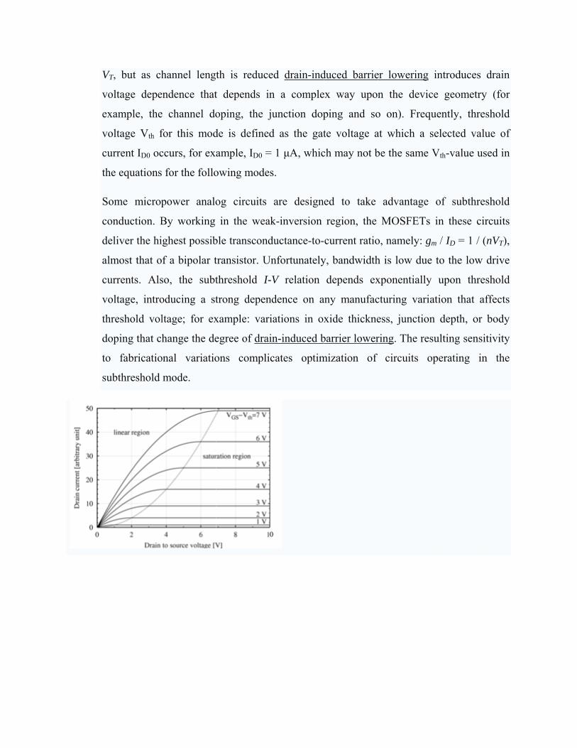
V
v
ex
v
cu
th
S
co
d
al
cu
v
th
d
to
su
VT, but as ch
oltage depe
xample, the
oltage Vth f
urrent ID0 oc
he equations
ome microp
onduction. B
eliver the hi
lmost that o
urrents. Als
oltage, intro
hreshold vol
oping that ch
o fabricatio
ubthreshold
hannel leng
endence that
e channel do
for this mod
ccurs, for ex
for the follo
power analo
By working
ghest possib
f a bipolar t
so, the subt
oducing a st
ltage; for ex
hange the de
onal variatio
mode.
th is reduce
t depends in
oping, the j
de is defined
ample, ID0 =
owing mode
og circuits
in the wea
ble transcond
transistor. U
threshold I-
trong depen
xample: vari
egree of drai
ons compli
ed drain-ind
n a comple
junction dop
d as the gat
= 1 µA, whic
s.
are design
ak-inversion
ductance-to-
Unfortunately
-V relation
ndence on a
iations in ox
in-induced b
cates optim
duced barrie
ex way upo
ping and so
te voltage a
ch may not b
ed to take
region, the
current ratio
y, bandwidth
depends ex
any manufac
xide thickne
barrier lower
mization of
er lowering
n the devic
o on). Frequ
at which a s
be the same V
advantage
MOSFETs
o, namely: gm
h is low due
xponentially
cturing varia
ess, junction
ring. The res
circuits o
introduces
ce geometry
uently, thres
selected valu
Vth-value us
of subthres
in these cir
m / ID = 1 / (
e to the low
upon thre
ation that af
n depth, or
sulting sensi
operating in
drain
y (for
shold
ue of
sed in
shold
rcuits
(nVT),
drive
shold
ffects
body
tivity
n the

4.0 Principle of operation
The following circuit was therefore designed.
Fig 4.1 Power quality monitor circuit
This design can detect spikes, noise overimposed in the mains, undervoltage overvoltage and
frequency instability.
5.0 Design simulation and results
C1470nF
R13.3kΩ
C2
470nF
C3470nF
R2
47kΩ
R3
5kΩKey=A 50%
LED1
LED2
R4270Ω
D1
1N4948GPD2
1N4948GP
T1
TS_AUDIO_VIRTUAL
XLV1
Input
R5
1kΩKey=A 50%
D31N4007
D5BT145_500R
R65.6kΩ
C4
470nF
C5470nF
C6570nF
C7
100uFC8
400nF
C9470nFC10
470nF
R73.9kΩ
R84.02kΩ
R947kΩ
R10
25kΩ
R1147kΩ
R122.2kΩ
R133.777kΩ
R143.9kΩ
D4
1N4007
D61N4007
D7
1N4007
D81N4007
U1
741
3
2
4
7
6
51
Q1ZVN4424G
LED3LED4
R16
5kΩ
R17
4.3kΩ
R18
5kΩ
VCC15V
VEE-15V
VDD-5V
T20
1
2
3
D9
1N4004
D10
1N4004
D11
1N4004
D12
1N4004
R19
1kΩ
V1
300 Vrms 50 Hz 0°
2
00
28
2726
25
VEE
VCC
VDD
24
23
20191816
17
15
1413
6
45
120
11
10
9
8731
XSC2
A B
Ext Trig+
+
_
_ + _
21
0
R20
10kΩKey=A 65%
29
22

The designed circuit was simulated using Multism pro-edition simulator. The result were as
shown below.
For the frequency monitor circuit the waveforms at various frequencies were as displayed in the
figures thereof.
At frequency of 0Hz there was no reading on the oscilloscope as shown.
At the frequency of 0Hz
At frequency of 15Hz

At frequency of 30Hz
At frequency of 45Hz
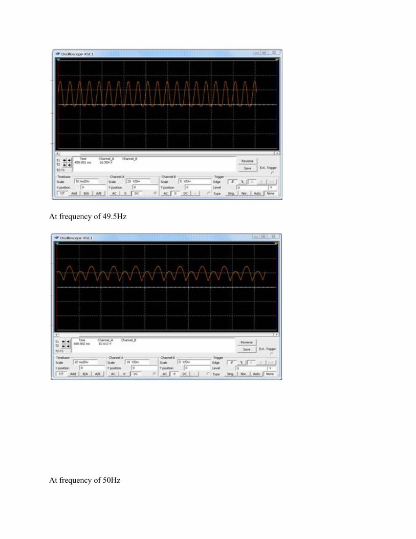
At frequency of 49.5Hz
At frequency of 50Hz
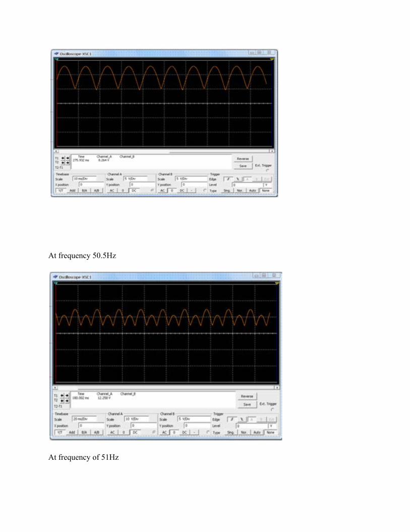
At frequency 50.5Hz
At frequency of 51Hz
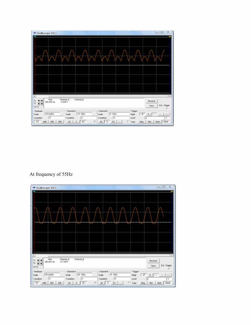
At frequency of 55Hz

Voltage monitor showing an over voltage

Showing normal operation at 230V

Input and output waveforms to overvoltage circuit

6.0 CONCLUSION AND RECOMMENDATION
The technique described in this report works well to detect transient disturbances on low-voltage
ac supply mains. These techniques can be applied to mains with any nominal frequency. While
this circuit was designed for use on single-phase mains, it could still be connected between one
three-phase line and neutral. The disturbance detector circuit can be used to trigger a digital
waveform recorder, as in our application, or operate a counter circuit to simply record the
occurrence of a disturbance. While the event counter is much less expensive, it does not provide
as much information. A low-cost commercial disturbance counter that transfers its data via a
telephone line to a remote computer is envisioned. Such counters could be located at electric
utility substations and in buildings with critical electrical equipment. The computer would
routinely interrogate each counter to determine at each site both (1) the average number of
disturbances per hour and (2) the duration and time of every outage. In addition, when there is an
abnormally large number of disturbances or a long-duration outage, the counters could call a
central computer and report the problem. Changes in the power quality at a site might possibly
be detected, and corrected, before the problem adversely affected operation of critical equipment.
Moreover, susceptible equipment could be interfaced to a local disturbance counter to improve
reliability of operation. When disturbances were occurring at unusually high rate, a computer, for
example, could make more frequent backups of its data to a nonvolatile medium.

REFERENCES
1.www.delab.com
2. COUGHLN R.F.``Operational Amplifiers and Linear Integrated circuits’’
3. Dr. Ogaba’s class notes on Power Electronics.
4. RASHID M., 1993`` Power Electronics’’
5. F.F. MAZDA,``Electronic Instruments and Measuring techniques’’
6. www.wikipedia.org