the nobel prize in chemistry, 2000: conductive polymers€¦ · conducting organic polymers:...
TRANSCRIPT
1
Information Department, P.O. Box 50005, SE-104 05 Stockholm, Sweden
Phone: +46 8 673 95 00, Fax: +46 8 15 56 70, E-mail: [email protected], Web site: www.kva.se __________________________________________________________________________ (Advanced Information) The Nobel Prize in Chemistry, 2000: Conductive polymers Contents Prize motivation 1 Conductive polymers – a surprising discovery 1 What is electrical conductivity? 2 What makes a material conductive? 3 Conductive polymers – the story 4 Applications of conductive polymers 5 Synthesis and processing 6 Mechanism of polymer conductivity – role of doping 6 Molecular electron-transfer theory 11 Electroluminescent polymers – second-generation conductive polymers 13 From silicon physics to molecular electronics 14 References and further reading 15 Prize motivation The Royal Swedish Academy of Sciences has decided to award the Nobel Prize in Chemistry for 2000 to three scientists who have revolutionised the development of electrically conductive polymers. Professor Alan J. Heeger at the University of California at Santa Barbara, USA Professor Alan G. MacDiarmid at the University of Pennsylvania, USA and Professor Hideki Shirakawa at the University of Tsukuba, Japan are rewarded “for the discovery and development of electrically conductive polymers”. The choice is motivated by the important scientific position that the field has achieved and the consequences in terms of practical applications and of interdisciplinary development between chemistry and physics. Conductive polymers – a surprising discovery We are used to polymers – that is, plastics – being somehow the opposite of metals. They insulate, they do not conduct electricity. Electric wires are coated with polymers to protect them – and us – from short-circuits. Yet Alan J. Heeger, Alan G. MacDiarmid and Hideki Shirakawa have changed this view with their discovery that a polymer, polyacetylene, can be made conductive almost like a metal. Polyacetylene was already known as a black powder when in 1974 it was prepared as a silvery film by Shirakawa and co-workers from acetylene, using a Ziegler-Natta catalyst (K. Ziegler and G. Natta, Nobel Prize in Chemistry 1966). But despite its metallic appearance it was not a conductor. In 1977, however, Shirakawa, MacDiarmid and Heeger discovered that oxidation with chlorine, bromine or iodine vapour made polyacetylene films 109 times more conductive than they were originally.1 Treatment with halogen was called “doping” by analogy with the doping of semiconductors. The “doped” form of polyacetylene had a conductivity of 105 Siemens per meter, which was higher than that of any previously known polymer. As a comparison, teflon has a conductivity of 10–16 S m–1and silver and copper 108 S m–1. A key property of a conductive polymer is the presence of conjugated double bonds along the backbone of the polymer. In conjugation, the bonds between the carbon atoms are alternately single and double. Every bond
2
contains a localised “sigma” (σ) bond which forms a strong chemical bond. In addition, every double bond also contains a less strongly localised “pi” (π) bond which is weaker. However, conjugation is not enough to make the polymer material conductive. In addition – and this is what the dopant does – charge carriers in the form of extra electrons or ”holes” have to be injected into the material. A hole is a position where an electron is missing. When such a hole is filled by an electron jumping in from a neighbouring position, a new hole is created and so on, allowing charge to migrate a long distance. Today conductive plastics are being developed for many uses, such as in corrosion inhibitors, compact capacitors, antistatic coating, electromagnetic shielding of computers, and in “smart” windows that can vary the amount of light they allow to pass, etc. A second generation of electric polymers has also appeared (see below) in, e.g., transistors, light-emitting diodes, lasers with further applications such as in flat television screens, solar cells, etc. Polymers have the potential advantages of low cost and that they can be processed, e.g., as film. We may soon be seeing electroluminescent plastics papered on walls for illumination. What is electrical conductivity? Conductivity is defined by Ohm’s law: U = R I, (1) where I is the current (in Amperes) through a resistor and U is the drop in potential (in Volts) across it. The proportionality constant R is called the “resistance”, measured in Ohms (Ω). R is measured by applying a known voltage across the resistor and measuring the current through it. The reciprocal of resistance (R–1) is called conductance. Ohm’s law is an empirical law, related to irreversible thermodynamics (Ilya Prigogine, Nobel Prize in Chemistry 1977), the flow I as a result of a gradient in potential leads to energy being dissipated (RI2 Joule s–1). Not all materials obey Ohm’s law. Gas discharges, vacuum tubes, semiconductors and what are termed one-dimensional conductors (e.g.a linear polyene chain) generally all deviate from Ohm’s law. In Ohmic material the resistance is proportional to the length l of the sample and inversely proportional to the sample cross-section A: R = ρ l / A (2) where ρ is the resistivity measured in Ω cm (in SI units Ω m). Its inverse σ = ρ–1 is the conductivity. The unit of conductance is the Siemens (S = Ω –1). The unit of conductivity is S m–1.
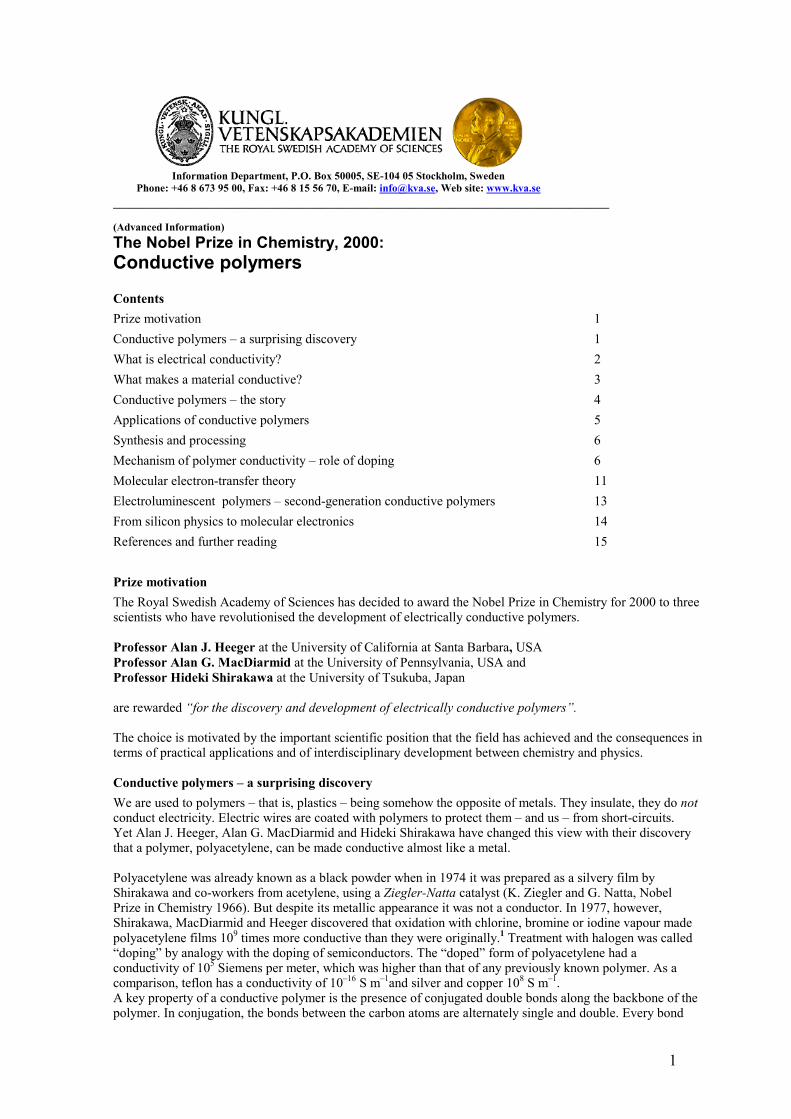
FIGURE 1 Conductivity of conductive polymers compared to those of other materials, from quartz (insulator) to copper (conductor). Polymers may also have conductivities corresponding to those of semiconductors. Conductivity depends on the number density of charge carriers (number of electrons n) and how fast they can move in the material (mobility µ): σ = n µ e (3) where -e is the electron charge. In semiconductors and electrolyte solutions, one must also add in Eq (3) an extra term due to positive charge carriers (holes or cations). Conductivity depends on temperature: it
3
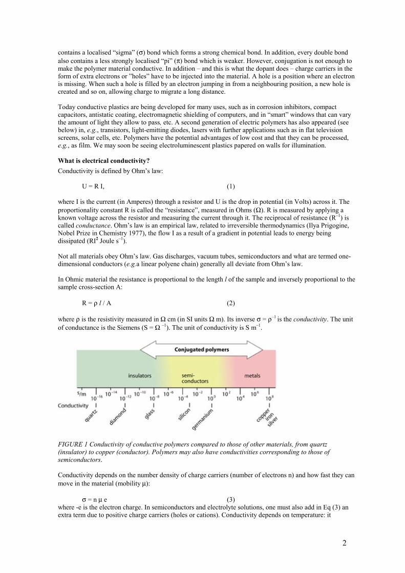
generally increases with decreasing temperature for “metallic” materials (some of which become superconductive below a certain critical temperature Tc), while it generally decreases with lowered temperature for semiconductors and insulators.
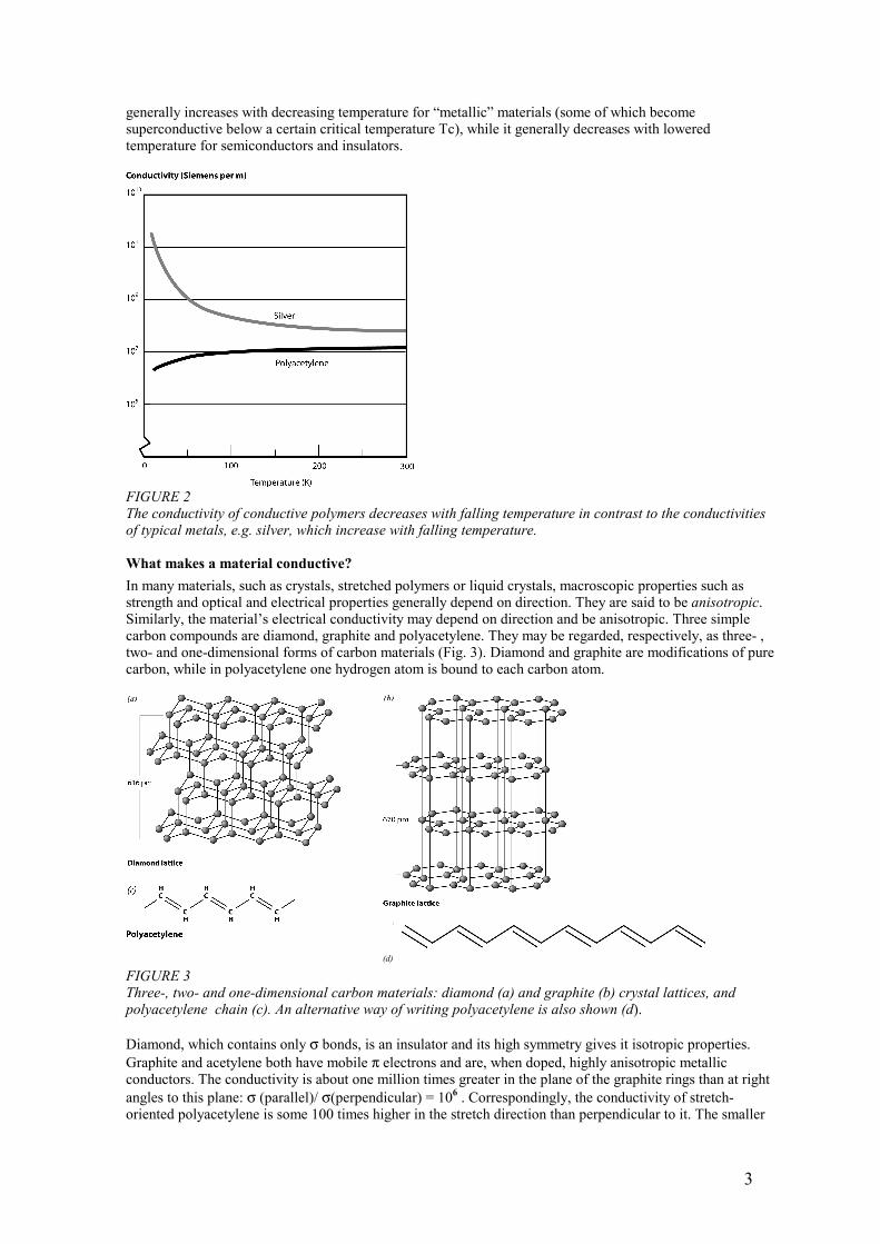
FIGURE 2 The conductivity of conductive polymers decreases with falling temperature in contrast to the conductivities of typical metals, e.g. silver, which increase with falling temperature. What makes a material conductive? In many materials, such as crystals, stretched polymers or liquid crystals, macroscopic properties such as strength and optical and electrical properties generally depend on direction. They are said to be anisotropic. Similarly, the material’s electrical conductivity may depend on direction and be anisotropic. Three simple carbon compounds are diamond, graphite and polyacetylene. They may be regarded, respectively, as three- , two- and one-dimensional forms of carbon materials (Fig. 3). Diamond and graphite are modifications of pure carbon, while in polyacetylene one hydrogen atom is bound to each carbon atom.
(d) FIGURE 3 Three-, two- and one-dimensional carbon materials: diamond (a) and graphite (b) crystal lattices, and polyacetylene chain (c). An alternative way of writing polyacetylene is also shown (d). Diamond, which contains only σ bonds, is an insulator and its high symmetry gives it isotropic properties. Graphite and acetylene both have mobile π electrons and are, when doped, highly anisotropic metallic conductors. The conductivity is about one million times greater in the plane of the graphite rings than at right angles to this plane: σ (parallel)/ σ(perpendicular) = 106 . Correspondingly, the conductivity of stretch-oriented polyacetylene is some 100 times higher in the stretch direction than perpendicular to it. The smaller

4
anisotropy compared to graphite, i.e. non-vanishing σ(perpendicular), could suggest ”short-circuiting” across the chains. Since the polyacetylene chains are not infinite, contacts between them are important if the material is to be macroscopically conductive. This could thus explain the lower conduction anisotropy compared to graphite Anisotropy is also interesting in other contexts of stretch aligned polymers: when the absorption of light is anisotropic the material acts as a polariser. Also mechanical strength is anisotropic: aligned polyacetylene fibers are known to be very strong along the orientation direction. Conductive polymers – the story Conductive polymers are a sub-group of a larger, older group of organic and inorganic electrical conductors. In fact, as early as 1862 H. Letheby of the College of London Hospital, by anodic oxidation of aniline in sulphuric acid, obtained a partly conductive material which was probably polyaniline. In the early 1970s, it was found that the inorganic explosive polymer, poly(sulphur nitride) (SN)x, was superconductive at extremely low temperatures (Tc=0.26 K). Many conductive organic compounds were also known, such as those discovered by K. Bechgaard (Copenhagen) together with D. Jerome (Paris) and famous for being superconductive at rather “high” temperatures (Tc around 10 K). They are salts of inorganic acceptors and organic donors consisting of large, cyclically conjugated π electron systems that form coin-pile stacks in the solid state. However, polyacetylene was the conductive polymer that actually launched this new field of research (Refs 1-4). For details of its history see the excellent review articles by Feast, et al., 5 and by M.G.Kanatzidis, 6 summarised below (see also Refs 7,8). Natta and co-workers prepared polyacetylene in 1958 by polymerising acetylene in hexane using Et3Al/Ti(OPr)4 (Et= ethyl, Pr=propyl) as a catalyst. Though the resulting material was highly crystalline and of regular structure, it was a black, air-sensitive, infusible and insoluble powder. Ziegler-Natta polymerisation was developed for polymerising alkenes such as ethylene by inserting an unsaturated molecule into the carbon-titanium bond of the growing macromolecule. It depends greatly on the activity of the choice of catalyst system. In the early 1970s Shirakawa and co-workers adapted the method to make well-defined films of polyacetylene. A major discovery by Shirakawa was that this polymerisation could be effected at the surface of a concentrated solution of the catalyst system in an inert solvent. The synthetic procedure involved adding Ti(OBu)4 and then Et3Al to a small volume of toluene under an inert atmosphere. The solution was allowed to age at 20oC for 45 minutes and was then cooled to –78oC. The reaction vessel was evacuated and acetylene gas introduced and allowed to react with a film of the catalyst which had already formed on the walls of the reaction vessel. A film of polyacetylene immediately formed there2. The reaction was controlled by evacuating unreacted acetylene gas. This procedure produced a copper-coloured film of all-cis-polyacetylene with a cis content of some 95 %. Shirakawa’s procedure also allowed silvery all-trans-polyacetylene to be formed by running the reaction in n-hexadecane at 150oC. However, its conductivity was relatively modest: cis-polyacetylene 10–8 -10–7 S m–1 and trans-polyacetylene 10–3 -10–2 S m–1.
FIGURE 4 All-cis- and all-trans-polyacetylene In 1975 Professors Alan Heeger and Alan MacDiarmid collaborated to study the metallic properties of a covalent inorganic polymer, (SN)x . They shifted their attention to polyacetylene after MacDiarmid had met

5
Shirakawa in Tokyo. During a visit at the University of Pennsylvania, Shirakawa refined the polymerisation of polyacetylene. With his experience from the (SN)x materials, MacDiarmid wanted to modify the polyacetylene by iodine treatment. Shirakawa and Ikeda had previously noted that treating silvery polyacetylene films with bromine or chlorine decreased the infrared transmission without altering the colour. MacDiarmid now turned to Heeger in whose laboratory a conductivity of 3000 S m–1 was measured for iodine-modified trans-polyacetylene, an increase of seven orders of magnitude over the undoped material. The seminal paper received for publication on May 16, 1977, had the title: Synthesis of electrically conducting organic polymers: Halogen derivatives of polyacetylene (CH)x. 1 Two other papers received later in the same year elaborated further on the topic. 3,4 Exciting experiments followed. Shirakawa could now control the ratio of cis/trans double bonds. Cis-polyacetylene doping resulted in even higher conductivities. The iodine may first have isomerized the polymer to all-trans material, which then underwent efficient (defect-free) doping so that the degree of orientation in the doped polyacetylene was greater overall. Doping cis-polyacetylene with AsF5 resulted in an increase of conductivity by a factor of 1011. The high conductivity found by Heeger, MacDiarmid and Shirakawa clearly opened up the field of “plastic electronics”. Other polymers studied extensively since the early 1980s include polypyrrole, polythiophene (and various polythiophene derivatives), polyphenylenevinylene and polyaniline. Polyacetylene remains the most crystalline conductive polymer but is not the first conductive polymer to be commercialised. This is because it is easily oxidised by the oxygen in air and is also sensitive to humidity. Polypyrrole and polythiophene differ from polyacetylene most notably in that they may be synthesised directly in the doped form and are very stable in air. Their conductivities are low, however: only around 104 S m–1, but this is enough for many practical purposes. Applications of conductive polymers The commercialisation exemplified by the following list of materials illustrates the effects of Heeger’s, McDiarmid’s and Shirakawa’s work on the later development of conductive polymers. The principal interest in the use of polymers is in low-cost manufacturing using solution-processing of film-forming polymers. Light displays and integrated circuits, for example, could theoretically be manufactured using simple inkjet printer techniques. 6-10 Doped polyaniline is used as a conductor and for electromagnetic shielding of electronic circuits. Polyaniline is also manufactured as a corrosion inhibitor. Poly(ethylenedioxythiophene) (PEDOT) doped with polystyrenesulfonic acid is manufactured as an anti-static coating material to prevent electrical discharge exposure on photographic emulsions and also serves as a hole injecting electrode material in polymer light-emitting devices. Poly(phenylene vinylidene) derivatives have been major candidates for the active layer in pilot production of electroluminescent displays (mobile telephone displays). Poly(dialkylfluorene) derivatives are used as the emissive layer in full-colour video matrix displays. Poly(thiophene) derivatives are promising for field-effect transistors: They may possibly find a use in supermarket checkouts. Poly(pyrrole) has been tested as microwave-absorbing “stealth” (radar-invisible) screen coatings and also as the active thin layer of various sensing devices. Other possible applications of conductive polymers include supercapacitors and electrolytic-type capacitors. Some conductive polymers such as polyaniline show a whole range of colours as a result of their many protonation and oxidation forms. Their electrochromic properties can be used to produce, e.g. “smart windows” that absorb sunlight in summer. An advantage over liquid crystals is that polymers can be fabricated in large sheets and unlimited visual angles. They do not generally respond as fast as in electron-gun displays, because the dopant needs time to migrate into or out from the polymer - but still fast enough for many applications. We shall return to electroluminescent polymers below.

6
Synthesis and processing There is often a big step between the first chemical synthesis of a molecular substance and the development of processing methods for practical applications. The first polyacetylenes were obtained from acetylene which polymerized in the presence of a catalyst. Of the two polyacetylene conformations, cis and trans, the trans form is thermodynamically more stable. Shirakawa’s polyacetylene had mainly the cis form and was a copper-coloured flexible film which could be converted to the silvery trans form by heating above 150° C. X-ray diffraction and scanning electron microscopy showed that such films were polycrystalline matted fibrils. These materials were semiconductors, the trans isomer with higher conductivity (4.4 x 10⁻³ S m–1) than the cis (1.7 x 10⁻⁷ S m–1). Shirakawa and Ikeda had noticed that when (CH)x films were exposed to bromine or chlorine at room temperature for a few minutes, there was a dramatic decrease in the infrared spectrum (decrease in transmission between 4000 and 400 cm–1). By contrast, complete halogenation, resulting in (CHBr)x, gave high IR transmission and a white film. However, they did not investigate the corresponding conductivity, so it remained for Heeger and McDiarmid, in collaboration, to discover the effect of doping. The halogen doping that transforms polyacetylene to a good conductor of electricity is oxidation (or p-doping). Reductive doping (called n-doping) is also possible using, e.g., an alkali metal. [CH]n + 3x/2 I 2 [CH]n x+ +xI3
– oxidative doping [CH] n + xNa [CH]n
x– + xNa + reductive doping The doped polymer is thus a salt. However, it is not the counter ions, I3
– or Na+, but the charges on the polymer that are the mobile charge carriers (see Mechanism of polymer conductivity, below). By applying an electric field perpendicular to the film, the counter ions can be made to diffuse from or into the structure, causing the doping reaction to proceed backwards or forwards. In this way the conductivity can be switched off or on. Processing polyacetylene and many other polymers such as polypyrrole and polythiophene was for a time ruled out because of their failure to melt or to dissolve in any solvent. Ingenious methods developed over the years have, however, made processing possible. In 1980, James W. Feast and co-workers at the University of Durham synthesised polyacetylene from a soluble precursor polymer, poly(7,8-bis(trifluoromethyl)-tricyclo[4.2.2.0]deca(3,7,9-triene). Upon heating, the dissociation product bis-trifluoromethylbenzene evaporates to leave a polyacetylene film which is much denser than Shirakawa’s material. Another important invention was Caltech researchers Robert H. Grubbs’ and co-workers’ production of polyacetylene by metathesis polymerisation of cyclooctatetraene in the presence of a titanium alkylidene complex as catalyst. Grubbs’ polyacetylene reportedly had a conductivity of about 35,000 S m–1, but was as intractable and unstable as other polyacetylenes. However, by attaching alkyl substituents to the cyclooctatetraene molecule, Grubbs and his group managed to prepare a soluble substituted polyacetylene that could be cast in any form desired, although the alkyl substituents seemed to lower the conductivity considerably. Another advance in electrical properties, but unfortunately not in processing, came in 1987 when BASF (Badishe Anilinen und Soda Fabrik) scientists Herbert Naarman and Nicholas Theophilou in West Germany developed a polymerisation method based on Shirakawa’s method, at 150°C. When doped, their material was claimed to have a conductivity of more than 107 Sm–1, i.e., of the same order as that of copper’s. This polyacetylene may have a higher conductivity because of its greater order and fewer defects than previous preparations. Other polymers with interesting properties have been developed: added to those already listed are polyparaphenylene, polyparaphenylenevinylene, polypyrrole, polythiophene and polyaniline and their derivatives. These materials generally show much lower conductivity than polyacetylene, ca 102–104 Sm–1, which is more than enough for many purposes. These polymers have the advantage of relatively high stability and processibility, e.g. poly(3-dodecylthiophene), can be prepared as a melt-spun, strong film in the undoped state and then doped to a conductivity of 105 Sm–1. Mechanism of polymer conductivity – role of doping In a metal there is a high density of electronic states with electrons with relatively low binding energy, and ”free electrons” move easily from atom to atom under an applied electric field. The conductivity of the material can be measured with standard procedures, a value for metallic copper around 108 S m–1 having been measured.
7
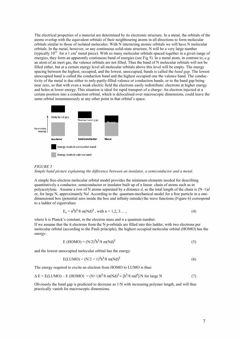
The electrical properties of a material are determined by its electronic structure. In a metal, the orbitals of the atoms overlap with the equivalent orbitals of their neighbouring atoms in all directions to form molecular orbitals similar to those of isolated molecules: With N interacting atomic orbitals we will have N molecular orbitals. In the metal, however, or any continuous solid-state structure, N will be a very large number (typically 1022 for a 1 cm3 metal piece). With so many molecular orbitals spaced together in a given range of energies, they form an apparently continuous band of energies (see Fig 5). In a metal atom, in contrast to, e.g. an atom of an inert gas, the valence orbitals are not filled. Thus the band of N molecular orbitals will not be filled either, but at a certain energy level all molecular orbitals above this level will be empty. The energy spacing between the highest, occupied, and the lowest, unoccupied, bands is called the band gap. The lowest unoccupied band is called the conduction band and the highest occupied one the valence band. The conduc-tivity of the metal is due either to only-partly-filled valence or conduction bands, or to the band gap being near zero, so that with even a weak electric field the electrons easily redistribute: electrons at higher energy and holes at lower energy. This situation is ideal for rapid transport of a charge: An electron injected at a certain position into a conduction orbital, which is delocalised over macroscopic dimensions, could leave the same orbital instantaneously at any other point in that orbital’s space.
FIGURE 5 Simple band picture explaining the difference between an insulator, a semiconductor and a metal. A simple free-electron molecular orbital model provides the minimum elements needed for describing quantitatively a conductor, semiconductor or insulator built up of a linear chain of atoms such as in polyacetylene. Assume a row of N atoms separated by a distance d, so the total length of the chain is (N–1)d or, for large N, approximately Nd. According to the quantum-mechanical model for a free particle in a one-dimensional box (potential zero inside the box and infinity outside) the wave functions (Figure 6) correspond to a ladder of eigenvalues En = n2h2/8 m(Nd)2 , with n = 1,2, 3… , (4) where h is Planck’s constant, m the electron mass and n a quantum number. If we assume that the π electrons from the N p-orbitals are filled into this ladder, with two electrons per molecular orbital (according to the Pauli principle), the highest occupied molecular orbital (HOMO) has the energy: E (HOMO) = (N/2)2h2/8 m(Nd)2 (5) and the lowest unoccupied molecular orbital has the energy: E(LUMO) = (N/2 + 1)2h2/8 m(Nd)2 (6) The energy required to excite an electron from HOMO to LUMO is thus: ∆ E = E(LUMO) – E (HOMO) = (N+1)h2/8 m(Nd)2 ≈ [h2/8 md2]/N for large N (7) Obviously the band gap is predicted to decrease as 1/N with increasing polymer length, and will thus practically vanish for macroscopic dimensions.

8
(b)
FIGURE 6 Free-electron model (one-dimensional box, length L): energy levels (a) and wavefunctions (b). The square of the wave function at a given position is the probability of finding the particle at that position. The model is adapted to multi-electron molecular orbital description: in (c) 16 electrons occupy the first eight molecular orbitals. The highest occupied molecular orbital is denoted HOMO, the next empty one LUMO. In (d) one electron from HOMO is promoted to LUMO (with retained opposite spins, i.e. S=0). Other models give qualitatively the same picture; e.g. the Hückel model for the π electron system or more advanced semi-empirical models and data programs, or ab initio models (e.g. the Gaussian programmes of John Pople, Nobel Prize in Chemistry 1998),which has a more or less regular energy ladder for the filled orbitals followed by a ladder of empty orbitals. The total wave function for the many-electron system occupies a state (in the simplest model it is the product of all the one-electron wave functions, i.e. the filled orbitals) and its energy is the energy of the whole system. With an even number of electrons, and two electrons occupying each of the orbitals of the lower part of the energy ladder, we have the situation described in Fig. 6 c, corresponding to the ground state. Since all electrons are paired, the total spin angular momentum S is zero, which means the substance is not magnetic. If an electron from one of the filled molecular orbitals is moved up into one of the empty molecular orbitals (Fig. 6 d), there is an excited electron configuration and a corresponding excited state with an energy higher than that of the ground state. The minimum energy difference between ground state and excited state – the band gap – corresponds to the energy needed to create a charge pair with one electron in the upper (empty) manifold of orbitals and one positive charge or ”hole” in lower (filled) manifold. If the spin of the remaining lone electron in the lower orbital and that of the excited electron are opposite each other, so that S is still zero (S=1/2 – 1/2=0), the excited state is a singlet state (not magnetic) whereas if the two spins are parallel, S = 1/2+1/2=1, the state is said to be a triplet state (paramagnetic, i.e., that the molecule has a permanent magnetic dipole moment due to electron spin). We saw that in our primitive free-electron picture (Eq 7) the band gap would vanish for a sufficiently long chain, so polyacetylene would thus be expected to behave as a conductor. Experimentally, the band gap is related to the wavelength of the first absorption band in the electronic spectrum of the substance. Thus a photon with wavelength λ can excite an electron from HOMO level to LUMO if the energy condition is fulfilled:
9
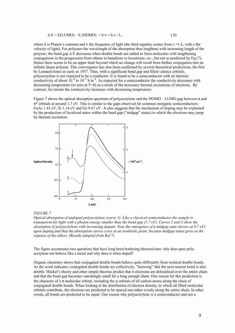
∆ E = E(LUMO) – E (HOMO) = h ν = h c / λ , ( 8) where h is Planck’s constant and ν the frequency of light (the third equality comes from c =ν λ, with c the velocity of light). For polyenes the wavelength of the absorption thus lengthens with increasing length of the polyene: the band gap ∆ E decreases when double bonds are added to form molecules with lengthening conjugations in the progression from ethene to butadiene to hexatriene, etc., but not as predicted by Eq (7). Hence there seems to be an upper limit beyond which no change will result from further conjugation into an infinite linear polyene. This convergence has also been confirmed by several theoretical predictions, the first by Lennard-Jones as early as 1937. Thus, with a significant band gap and filled valence orbitals, polyacetylene is not expected to be a conductor. It is found to be a semiconductor with an intrinsic conductivity of about 10–5 to 10–7 S m–1. As expected for a semiconductor the conductivity decreases with decreasing temperature (to zero at T=0) as a result of the necessary thermal excitations of electrons. By contrast, for metals the conductivity increases with decreasing temperature. Figure 7 shows the optical absorption spectrum of polyacetylene and the HOMO – LUMO gap between π and π* orbitals at around 1.7 eV. This is similar to the gaps observed for common inorganic semiconductors: GaAs 1.43 eV, Si 1.14 eV and Ge 0.67 eV . It also suggests that the mechanism of doping may be explained by the production of localized states within the band gap (”midgap” states) to which the electrons may jump by thermal excitation.
FIGURE 7 Optical absorption of undoped polyacetylene (curve 1). Like a classical semiconductor the sample is transparent for light with a photon energy smaller than the band gap (1.7 eV). Curves 2 and 3 show the absorption of polyacetylene with increasing dopant. Note the emergence of a midgap state (arrow at 0.7 eV) upon doping and that the absorption curves cross at an isosbestic point, because midgap states grow at the expense of the others. (Results adapted from Ref 7) The figure accentuates two questions that have long been bothering theoreticians: why does pure poly-acetylene not behave like a metal and why does it when doped? Organic chemistry shows that conjugated double bonds behave quite differently from isolated double bonds. As the word indicates, conjugated double bonds act collectively, ”knowing” that the next-nearest bond is also double. Hückel’s theory and other simple theories predict that π electrons are delocalised over the entire chain and that the band gap becomes vanishingly small for a long enough chain. One reason for this prediction is the character of a π molecular orbital, including the p orbitals of all carbon atoms along the chain of conjugated double bonds. When looking at the distribution of electron density, to which all filled molecular orbitals contribute, the electrons are predicted to be spaced out rather evenly along the entire chain. In other words, all bonds are predicted to be equal. One reason why polyacetylene is a semiconductor and not a
10
conductor is due to that the bonds are not equal: there is a distinct alternation, every second bond having some double-bond character, almost like in Fig. 3 c. This idea came in the 1930’s from Heisenberg’s student Peierls who showed that a hypothetical chain of equidistantly spaced sodium atoms is unstable and will undergo a metal-to-insulator transition at low temperatures, by changing the equidistant spacing of atom nuclei into one with alternating short and long distances. This deformation is related to the Jahn-Teller distortion undergone by a system with degenerate states, e.g., when a hole is created in a closed shell configuration. One familiar example of the Jahn-Teller effect is the structure of the complex ion [Cu(H2O) 6] 2+. Here, the d9 configuration makes only three electrons go into the degenerate d z2 and dx2-y2 orbitals, lobes towards the corners of the co-ordination octahedron. Lowering the symmetry, e.g., by moving the two water molecules along the z axis away from the Cu2+ ion, lifts degeneracy: the energy of the doubly-filled d z2 orbital is thereby lowered and the energy of the singly-filled dx2-y2 is raised. This structural distortion thus lowers the total energy of the complex ion. In the case of the Peierls distortion, a small conformational distortion would be enough to increase the band gap and make polyacetylene a semiconductor or even insulator. The role of the dopant is either to remove or to add electrons to the polymer. For example, iodine (I2) will abstract an electron under formation of an I3
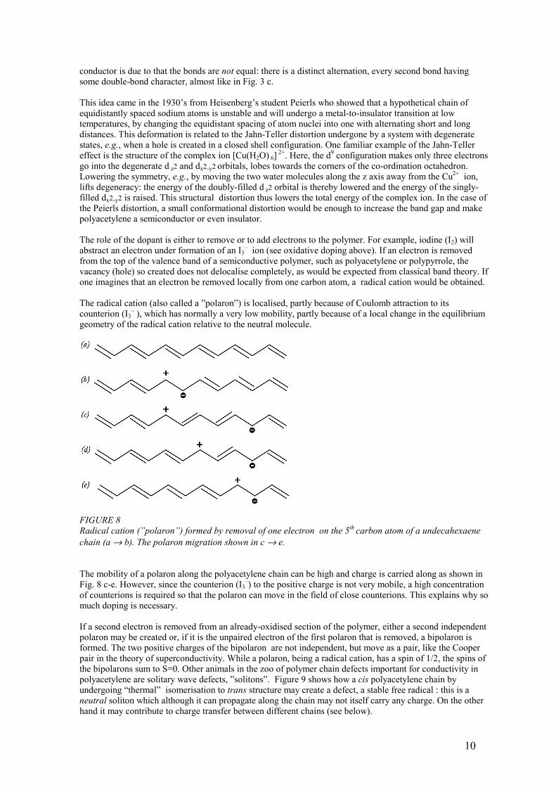
– ion (see oxidative doping above). If an electron is removed from the top of the valence band of a semiconductive polymer, such as polyacetylene or polypyrrole, the vacancy (hole) so created does not delocalise completely, as would be expected from classical band theory. If one imagines that an electron be removed locally from one carbon atom, a radical cation would be obtained. The radical cation (also called a ”polaron”) is localised, partly because of Coulomb attraction to its counterion (I3
– ), which has normally a very low mobility, partly because of a local change in the equilibrium geometry of the radical cation relative to the neutral molecule.
FIGURE 8 Radical cation (”polaron”) formed by removal of one electron on the 5th carbon atom of a undecahexaene chain (a → b). The polaron migration shown in c → e. The mobility of a polaron along the polyacetylene chain can be high and charge is carried along as shown in Fig. 8 c-e. However, since the counterion (I3
–) to the positive charge is not very mobile, a high concentration of counterions is required so that the polaron can move in the field of close counterions. This explains why so much doping is necessary. If a second electron is removed from an already-oxidised section of the polymer, either a second independent polaron may be created or, if it is the unpaired electron of the first polaron that is removed, a bipolaron is formed. The two positive charges of the bipolaron are not independent, but move as a pair, like the Cooper pair in the theory of superconductivity. While a polaron, being a radical cation, has a spin of 1/2, the spins of the bipolarons sum to S=0. Other animals in the zoo of polymer chain defects important for conductivity in polyacetylene are solitary wave defects, ”solitons”. Figure 9 shows how a cis polyacetylene chain by undergoing “thermal” isomerisation to trans structure may create a defect, a stable free radical : this is a neutral soliton which although it can propagate along the chain may not itself carry any charge. On the other hand it may contribute to charge transfer between different chains (see below).

11
FIGURE 9 A soliton is created by isomerisation of cis polyacetylene (a → b) and moves by pairing to an adjacent electron (b → e). However, generally solitons made by doping are more important than “bond alternation defects” like the one illustrated in the figure. For an animated version, see www.nobel.se/announcement/2000 , showing two polarons created by oxidation by iodine followed by spin migration leading to the formation of two carbo cations (positive solitons) and their migration along the chain when subjected to an electric field. Bulk conductivity in the polymer material is limited by the need for the electrons to jump from one chain to the next, i.e., in molecular terms an intermolecular charge transfer reaction. It is also limited by macroscopic factors such as bad contacts between different crystalline domains in the material. One mechanism proposed to account for conductivity by charge-hopping between different polymer chains is ”intersoliton hopping” (Figure 10). Here an electron is jumping between localized states on adjacent polymer chains; the role of the soliton is to move around and to exchange an electron with a closely located charged soliton, which is localised. The mechanism at work in intersoliton hopping is very similar to that operating in most conducting polymers somewhere in between the metallic state at high doping and the semiconducting state at very low doping. All conjugated polymers do not carry solitons, but polarons can be found in most of them. Charge transport in polaron-doped polymers occurs via electron transfer between localized states being formed by charge injection on the chain. 13
FIGURE 10 Intersoliton hopping: charged solitons (bottom) are trapped by dopant counterions, while neutral solitons (top) are free to move. A neutral soliton on a chain close to one with a charged soliton can interact: the electron hops from one defect to the other. Molecular electron-transfer theory Electron transfer (ET) reactions, which are also redox reactions, are among the most common and simple chemical reactions. The electron donor is oxidised and the acceptor reduced. The free energy that drives the reaction is the difference in reduction potentials between donor and acceptor. One type of ET reaction, charge separation, takes place after photo-excitation to an upper potential energy surface (PES). For example, in photosynthesis a series of ET reactions all start from a photo-induced charge separation. The molecular electron transfer theory based on contributions by Rudolph Marcus (Nobel Prize in Chemistry 1992), 14 so far mainly applied to biopolymers rather than truly conductive polymers, will be briefly explained here.

12
An electron transfer reaction corresponds to motion on a potential energy surface between two minima, corresponding to different stable localisations of an electron. With a naphthalene cation together with an anthracene molecule, the following electron transfer reaction may then take place:
Consider the whole system [(C10H8)(C14H10)]+. There are two local minima on its energy surface: one for [(C10H8)+ (C14H10)] corresponding to the reactant state and one for [(C10H8)(C14H10)+] corresponding to the product state. The latter corresponds to the lowest minimum.
It is not hard to imagine why there is a barrier between the two minima. At the left (reactant) minimum the bond lengths are those for the naphthalene cation - neutral anthracene combination. At the right (product) minimum the bond lengths refer to neutral naphthalene and anthracene cation. The local minima, QR for the reactant state and QP for the product state, are each approximately parabolic: if we move any of the atoms away from its equilibrium position by change dQ in bond length or bond angle, the energy would increase by (k/2)dQ2, where k is a force constant corresponding to this deformation. Another contribution to the barrier comes from the solvent. If a dissolved charged molecule changes its charge distribution, the solvent molecules reorient themselves to minimise the total energy. In the Marcus model14 the PESs are approximated by interacting parabolas. This model uses the important fact that the structure undergoes only a rather small change, compared to other chemical reactions, in the ET reaction. Figure 11 assumes that ∆G°=0 (parabolas of equal height).
FIGURE 11 Two parabolic potential energy graphs corresponding to the energy for reactant and product states in an electron transfer reaction. ∆G* is the activation barrier that has to be overcome and λ is the ”reorganisation energy”. The fundamental equation for the rate in the Marcus model derives from the Arrhenius and Eyring rate equation: k = ν κ e(-∆G*/ kT) (9)
Energy
Reaction coordinate
13
where ν is the frequency of a vibration corresponding to the number of attempts per unit time to ascend the barrier. κ is a transmission coefficient. ∆G* is the height of the barrier. In the Marcus model another quantity is needed: reorganisation energy (λ). If the free energy change ∆G0 for the reaction is zero (Fig 12), λ is in the simplest case the vertical energy difference from the minimum of one parabola up to the other parabola. If ∆G0 is negative the ET reaction is spontaneous and will run from left to right. In this case the right parabola is lower than the left by the amount –∆G0. We then have the following activation energy: ∆G* = (λ/4)( 1 + ∆G°/λ)2 (10) The activation energy obviously disappears if –∆G0=λ. If an electrical field is applied so that, e.g., the right (product) parabola is lowered, i.e., ∆G° is more negative, this will also lead to a reduction in the activation energy ∆G* .From this follows that if a field is applied, the electron leaps more easily between donor and acceptor. The Marcus model has been mainly applied to electron transfer reactions in biomolecular contexts and in a few cases also to semiconductive polymers. 15 Electroluminescent polymers – second-generation conductive polymers Since the first report of metallic conductivities in ”doped” polyacetylene in 1977, the science of conductive polymers has advanced rapidly in various directions. 6,9,10 More recently, as high-purity polymers have become available, a range of semiconductor devices has been investigated. These include normal transistors and field-effect transistors (FET), and photodiodes and light-emitting diodes (LEDs). In particular, polymer LEDs now show attractive characteristics, including efficient light generation, with great potential for commercialisation. Again the principal interest in polymers is in their potential use for rapid, low-cost processing using film-forming polymer solutions. Like the conductive polymers, the semi-conductive polymers obtain their properties from their conduction-molecular orbitals and valence molecular orbitals, i.e. bonding π orbitals and antibonding π* orbitals, respectively. In electro-chemical light emitting cells, the semi-conductive polymer could be surrounded asymmetrically with a hole-injecting electrode (usually ITO) on one side, and a low work function, electron injecting metal contact (e.g., aluminum, magnesium or calcium) on the other side. The emission of light is then the result of radiative charge carrier recombination in the polymer as electrons from one side and holes from the other recombine. Electroluminescence from conjugated polymers was first reported in 1990.9 Poly(p-phenylene vinylene), PPV, was used as the single semiconductor layer. In light-emitting diode polymers, the semi-conductive polymer could be surrounded asymmetrically with a hole-injecting electrode (transparent ITO) on one side, and a low work function, electron-injecting metal contact (e.g. aluminium, magnesium or calcium) on the other side. With proper bias, electrons and holes are injected, which meet in bulk of the polymer film. The emission of light is then the result of radiative charge carrier recombination in the polymer film. PPV has an energy gap between the LUMO (π) and ΗΟΜΟ (π*) orbitals of about 2.5 eV, and thus produces (according to Eq 8) yellow-green luminescence, with the same emission spectrum as that produced by normal photo excitation of the conjugated polymer. Much higher efficiencies have been reported for LED polymer diodes in which a layer of poly(dioxyethylene thienylene) doped with polystyrene sulphonic acid or polyaniline-chloride is inserted between the indium-tin oxide and the emissive polymer layers. Two conjugated polymers, with different emission colours, used for LED fabrication, are shown in Fig 12, together with a schematic drawing of how such a device can be constructed.

14
FIGURE 12 a. Semiconductor polymers (left) with different emission colours together with a conductive electrode polymer (right) used for fabrication of light-emitting diodes (LEDs). b. Cross section of polymer LED .
From silicon physics to molecular electronics Chemistry is currently moving centre-stage in solid-state physics to give us a novel basis for materials science and thus for most new technologies. The chemist can design novel molecules in which neighbouring atoms are kept in position, creating “short-range” order even in amorphous solids and liquid solutions. In solid-state physics a precondition for a perfect crystal is long-range order as well. Regular structure is generally a ‘must’ for achieving the unique macroscopic optical and electrical properties needed for generating harmonics to double the frequency of laser light or for super-conductivity. Solid-state physics is traditionally based on silicon. Chemistry is now offering greater microscopic variability in the myriad ways the atoms of the periodic table may be combined into molecules with complex higher-order structures. A protein molecule, for example, is a polymer chain composed mainly of carbon, oxygen, nitrogen and hydrogen atoms. As a result of interactions between different parts of the chain (including short side chains) it can fold itself into a well determined three-dimensional structure, thus achieving long-range order. By choosing adequate substituents, the chemist can further control the intrinsic electronic properties by distributing the electrons in space in a specific way. Today’s electronics technology is based on the use of single crystals that are large compared to the molecular scale. The crystals are fused together, macroscopically doped and connected to big electrodes to form diodes, transistors etc. Now, however, with advances in manipulation techniques such as high-resolution optical lithography small, self-contained, electronic devices can be manufactured. For the most advanced integrated circuits on a single silicon wafer, minimum pattern dimensions are some 200 nm.17, 18 This is still one order of

15
magnitude larger than the dimensions of molecules, and more than two orders of magnitude larger than the Ångström resolution that can be designed within a molecule. The dream is thus to put electronic circuit properties into single molecules. Arrays of such molecules – possibly connected by conductive-polymer wires – on molecular scaffoldings would form molecular wafers. One may speculate that reduced dimensions from 200 nm to, say, 2 Å, and the concomitant shrinkage in circuit size could increase the speed and dynamic memory of computers by a factor of 108. Such progress would correspond to forty years of computer technology development. Conductive polymers may become crucial for the building of such a molecular electronics world. Bengt Nordén Chairman of the Nobel Committee for Chemistry, Professor of Physical Chemistry, Chalmers University of Technology, Sweden Eva Krutmeijer Press Officer, the Royal Swedish Academy of Sciences, [email protected] References and further reading Conductive polymers 1. H. Shirakawa, E.J. Louis, A.G. MacDiarmid, C.K. Chiang and A.J. Heeger, J Chem Soc Chem Comm (1977) 579 2. T. Ito, H. Shirakawa and S. Ikeda, J.Polym.Sci.,Polym.Chem. Ed. 12 (1974) 11–20 3. C.K. Chiang, C.R. Fischer, Y.W. Park, A.J. Heeger, H. Shirakawa, E.J. Louis, S.C. Gau and A.G.
MacDiarmid , Phys. Rev. Letters 39 (1977) 1098 4. C.K. Chiang, M.A. Druy, S.C. Gau, A.J. Heeger, E.J. Louis, A.G. MacDiarmid*, Y.W. Park and H.
Shirakawa, J. Am. Chem. Soc. 100 (1978) 1013 5. Feast, W.J., Tsibouklis, J., Pouwer, K.L., Gronendaal, L. and Meijer, E.W. Polymer 37 (1996) 5017 6. M.G. Kanatzidis Chem. Eng. News 3 (1990) 36 7. Roth, S. ”One-Dimensional Metals” Weinheim VCH, 1995 8. Nobel Symposium in Chemistry: Conjugated Polymers and Related Materials: The Interconnection
of Chemical and Electronic Structure, W. R. Salaneck, I. Lundström, and B. Rånby, Ed’s (Oxford Sci., Oxford, 1993)
Electroluminescence in conjugated polymers 9. J.H. Burroughes, D.D.C. Bradley, A.R. Brown, R.N. Marks, K. Mackay, R.H. Friend, P.L. Burns and
A.B. Holmes Nature 347 (1990) 539 10. R.H. Friend, R.W. Gymer, A.B. Holmes, J.H. Burroughes, R.N. Marks, C. Taliani, D.D.C. Bradley,
D.A. Dos Santos, J.L. Bredas, M. Lögdlund and W.R. Salaneck Nature 397 (1999) 121 11. L.B. Groenendaal, F. Jonas, D. Freitag, H. Pielartzik, and J.R. Reynolds
Adv. Mater. 12(7) (2000) 481 12. Light-Emitting Diodes with Variable Colours from Polymer Blends.
M. Berggren, O. Inganäs, G. Gustafsson, J.C. Gustafsson-Carlberg, J. Rasmusson, M.R. Andersson, T. Hjertberg and O. Wennerström. Nature 372, (1994) 444

16
Molecular electron transfer theory 13. M. Winokur, Y.B. Moon, A.J. Heeger, J. Barker, D.C. Bott, and H. Shirakawa, Phys. Rev. Letters
58, 2329 (1987) 14. R.A. Marcus, J. Chem. Phys. 36, 966, 979 (1956); Annual Rev. Phys. Chem 15 (1964) 155 15. S. Larsson and L. Rodriguez-Monge, Int. J. Quant. Chem. 63 (1997) 655 Electronics technology 16. D. de Leeuw Plastic electronics Physics World March (1999) 31 17. R.E. Gleason ”How far will circuits shrink?” Science Spectra 20 (2000) 32.