principles of asynchronous circuit design – a systems perspective
TRANSCRIPT
PRINCIPLES OFASYNCHRONOUS CIRCUIT DESIGN– A Systems Perspective
Edited by
JENS SPARSØTechnical University of Denmark
STEVE FURBERThe University of Manchester, UK
Kluwer Academic PublishersBoston/Dordrecht/London
Contents
Preface xi
Part I Asynchronous circuit design – A tutorial
Author: Jens Sparsø
1Introduction 3
1.1 Why consider asynchronous circuits? 31.2 Aims and background 41.3 Clocking versus handshaking 51.4 Outline of Part I 8
2Fundamentals 9
2.1 Handshake protocols 92.1.1 Bundled-data protocols 92.1.2 The 4-phase dual-rail protocol 112.1.3 The 2-phase dual-rail protocol 132.1.4 Other protocols 13
2.2 The Muller C-element and the indication principle 142.3 The Muller pipeline 162.4 Circuit implementation styles 17
2.4.1 4-phase bundled-data 182.4.2 2-phase bundled data (Micropipelines) 192.4.3 4-phase dual-rail 20
2.5 Theory 232.5.1 The basics of speed-independence 232.5.2 Classification of asynchronous circuits 252.5.3 Isochronic forks 262.5.4 Relation to circuits 26
2.6 Test 272.7 Summary 28
3Static data-flow structures 29
3.1 Introduction 293.2 Pipelines and rings 30
v
vi PRINCIPLES OF ASYNCHRONOUS CIRCUIT DESIGN
3.3 Building blocks 313.4 A simple example 333.5 Simple applications of rings 35
3.5.1 Sequential circuits 353.5.2 Iterative computations 35
3.6 FOR, IF, and WHILE constructs 363.7 A more complex example: GCD 383.8 Pointers to additional examples 39
3.8.1 A low-power filter bank 393.8.2 An asynchronous microprocessor 393.8.3 A fine-grain pipelined vector multiplier 40
3.9 Summary 40
4Performance 41
4.1 Introduction 414.2 A qualitative view of performance 42
4.2.1 Example 1: A FIFO used as a shift register 424.2.2 Example 2: A shift register with parallel load 44
4.3 Quantifying performance 474.3.1 Latency, throughput and wavelength 474.3.2 Cycle time of a ring 494.3.3 Example 3: Performance of a 3-stage ring 514.3.4 Final remarks 52
4.4 Dependency graph analysis 524.4.1 Example 4: Dependency graph for a pipeline 524.4.2 Example 5: Dependency graph for a 3-stage ring 54
4.5 Summary 56
5Handshake circuit implementations 57
5.1 The latch 575.2 Fork, join, and merge 585.3 Function blocks – The basics 60
5.3.1 Introduction 605.3.2 Transparency to handshaking 615.3.3 Review of ripple-carry addition 64
5.4 Bundled-data function blocks 655.4.1 Using matched delays 655.4.2 Delay selection 66
5.5 Dual-rail function blocks 675.5.1 Delay insensitive minterm synthesis (DIMS) 675.5.2 Null Convention Logic 695.5.3 Transistor-level CMOS implementations 705.5.4 Martin’s adder 71
5.6 Hybrid function blocks 735.7 MUX and DEMUX 755.8 Mutual exclusion, arbitration and metastability 77
5.8.1 Mutual exclusion 775.8.2 Arbitration 795.8.3 Probability of metastability 79
Contents vii
5.9 Summary 80
6Speed-independent control circuits 81
6.1 Introduction 816.1.1 Asynchronous sequential circuits 816.1.2 Hazards 826.1.3 Delay models 836.1.4 Fundamental mode and input-output mode 836.1.5 Synthesis of fundamental mode circuits 84
6.2 Signal transition graphs 866.2.1 Petri nets and STGs 866.2.2 Some frequently used STG fragments 88
6.3 The basic synthesis procedure 916.3.1 Example 1: a C-element 926.3.2 Example 2: a circuit with choice 926.3.3 Example 2: Hazards in the simple gate implementation 94
6.4 Implementations using state-holding gates 966.4.1 Introduction 966.4.2 Excitation regions and quiescent regions 976.4.3 Example 2: Using state-holding elements 986.4.4 The monotonic cover constraint 986.4.5 Circuit topologies using state-holding elements 99
6.5 Initialization 1016.6 Summary of the synthesis process 1016.7 Petrify: A tool for synthesizing SI circuits from STGs 1026.8 Design examples using Petrify 104
6.8.1 Example 2 revisited 1046.8.2 Control circuit for a 4-phase bundled-data latch 1066.8.3 Control circuit for a 4-phase bundled-data MUX 109
6.9 Summary 113
7Advanced 4-phase bundled-data
protocols and circuits115
7.1 Channels and protocols 1157.1.1 Channel types 1157.1.2 Data-validity schemes 1167.1.3 Discussion 116
7.2 Static type checking 1187.3 More advanced latch control circuits 1197.4 Summary 121
8High-level languages and tools 123
8.1 Introduction 1238.2 Concurrency and message passing in CSP 1248.3 Tangram: program examples 126
8.3.1 A 2-place shift register 1268.3.2 A 2-place (ripple) FIFO 126
viii PRINCIPLES OF ASYNCHRONOUS CIRCUIT DESIGN
8.3.3 GCD using while and if statements 1278.3.4 GCD using guarded commands 128
8.4 Tangram: syntax-directed compilation 1288.4.1 The 2-place shift register 1298.4.2 The 2-place FIFO 1308.4.3 GCD using guarded repetition 131
8.5 Martin’s translation process 1338.6 Using VHDL for asynchronous design 134
8.6.1 Introduction 1348.6.2 VHDL versus CSP-type languages 1358.6.3 Channel communication and design flow 1368.6.4 The abstract channel package 1388.6.5 The real channel package 1428.6.6 Partitioning into control and data 144
8.7 Summary 146Appendix: The VHDL channel packages 148A.1 The abstract channel package 148A.2 The real channel package 150
Part II Balsa - An Asynchronous Hardware Synthesis System
Author: Doug Edwards, Andrew Bardsley
9An introduction to Balsa 155
9.1 Overview 1559.2 Basic concepts 1569.3 Tool set and design flow 1599.4 Getting started 159
9.4.1 A single-place buffer 1619.4.2 Two-place buffers 1639.4.3 Parallel composition and module reuse 1649.4.4 Placing multiple structures 165
9.5 Ancillary Balsa tools 1669.5.1 Makefile generation 1669.5.2 Estimating area cost 1679.5.3 Viewing the handshake circuit graph 1689.5.4 Simulation 168
10The Balsa language 173
10.1 Data types 17310.2 Data typing issues 17610.3 Control flow and commands 17810.4 Binary/unary operators 18110.5 Program structure 18110.6 Example circuits 18310.7 Selecting channels 190
Contents ix11Building library components 193
11.1 Parameterised descriptions 19311.1.1 A variable width buffer definition 19311.1.2 Pipelines of variable width and depth 194
11.2 Recursive definitions 19511.2.1 An n-way multiplexer 19511.2.2 A population counter 19711.2.3 A Balsa shifter 20011.2.4 An arbiter tree 202
12A simple DMA controller 205
12.1 Global registers 20512.2 Channel registers 20612.3 DMA controller structure 20712.4 The Balsa description 211
12.4.1 Arbiter tree 21112.4.2 Transfer engine 21212.4.3 Control unit 213
Part III Large-Scale Asynchronous Designs
13Descale 221Joep Kessels & Ad Peeters, Torsten Kramer andVolker Timm
13.1 Introduction 22213.2 VLSI programming of asynchronous circuits 223
13.2.1 The Tangram toolset 22313.2.2 Handshake technology 22513.2.3 GCD algorithm 226
13.3 Opportunities for asynchronous circuits 23113.4 Contactless smartcards 23213.5 The digital circuit 235
13.5.1 The 80C51 microcontroller 23613.5.2 The prefetch unit 23913.5.3 The DES coprocessor 241
13.6 Results 24313.7 Test 24513.8 The power supply unit 24613.9 Conclusions 247
14An Asynchronous Viterbi Decoder 249Linda E. M. Brackenbury
14.1 Introduction 24914.2 The Viterbi decoder 250
14.2.1 Convolution encoding 25014.2.2 Decoder principle 251
14.3 System parameters 25314.4 System overview 254
x PRINCIPLES OF ASYNCHRONOUS CIRCUIT DESIGN
14.5 The Path Metric Unit (PMU) 25614.5.1 Node pair design in the PMU 25614.5.2 Branch metrics 25914.5.3 Slot timing 26114.5.4 Global winner identification 262
14.6 The History Unit (HU) 26414.6.1 Principle of operation 26414.6.2 History Unit backtrace 26414.6.3 History Unit implementation 267
14.7 Results and design evaluation 26914.8 Conclusions 271
14.8.1 Acknowledgement 27214.8.2 Further reading 272
15Processors 273Jim D. Garside
15.1 An introduction to the Amulet processors 27415.1.1 Amulet1 (1994) 27415.1.2 Amulet2e (1996) 27515.1.3 Amulet3i (2000) 275
15.2 Some other asynchronous microprocessors 27615.3 Processors as design examples 27815.4 Processor implementation techniques 279
15.4.1 Pipelining processors 27915.4.2 Asynchronous pipeline architectures 28115.4.3 Determinism and non-determinism 28215.4.4 Dependencies 28815.4.5 Exceptions 297
15.5 Memory – a case study 30215.5.1 Sequential accesses 30215.5.2 The Amulet3i RAM 30315.5.3 Cache 307
15.6 Larger asynchronous systems 31015.6.1 System-on-Chip (DRACO) 31015.6.2 Interconnection 31015.6.3 Balsa and the DMA controller 31215.6.4 Calibrated time delays 31315.6.5 Production test 314
15.7 Summary 315
Epilogue 317
References 319
Index 333
Preface
This book was compiled to address a perceived need for an introductory texton asynchronous design. There are several highly technical books on aspects ofthe subject, but no obvious starting point for a designer who wishes to becomeacquainted for the first time with asynchronous technology. We hope this bookwill serve as that starting point.
The reader is assumed to have some background in digital design. We as-sume that concepts such as logic gates, flip-flops and Boolean logic are famil-iar. Some of the latter sections also assume familiarity with the higher levels ofdigital design such as microprocessor architectures and systems-on-chip, butreaders unfamiliar with these topics should still find the majority of the bookaccessible.
The intended audience for the book comprises the following groups:
Industrial designers with a background in conventional (clocked) digitaldesign who wish to gain an understanding of asynchronous design inorder, for example, to establish whether or not it may be advantageousto use asynchronous techniques in their next design task.
Students in Electronic and/or Computer Engineering who are taking acourse that includes aspects of asynchronous design.
The book is structured in three parts. Part I is a tutorial in asynchronousdesign. It addresses the most important issue for the beginner, which is how tothink about asynchronous systems. The first big hurdle to be cleared is that ofmindset – asynchronous design requires a different mental approach from thatnormally employed in clocked design. Attempts to take an existing clockedsystem, strip out the clock and simply replace it with asynchronous handshakesare doomed to disappoint. Another hurdle is that of circuit design methodol-ogy – the existing body of literature presents an apparent plethora of disparateapproaches. The aim of the tutorial is to get behind this and to present a singleunified and coherent perspective which emphasizes the common ground. Inthis way the tutorial should enable the reader to begin to understand the char-acteristics of asynchronous systems in a way that will enable them to ‘think
xi
xii PRINCIPLES OF ASYNCHRONOUS CIRCUIT DESIGN
outside the box’ of conventional clocked design and to create radical new de-sign solutions that fully exploit the potential of clockless systems.
Once the asynchronous design mindset has been mastered, the second hur-dle is designer productivity. VLSI designers are used to working in a highlyproductive environment supported by powerful automatic tools. Asynchronousdesign lags in its tools environment, but things are improving. Part II of thebook gives an introduction to Balsa, a high-level synthesis system for asyn-chronous circuits. It is written by Doug Edwards (who has managed the Balsadevelopment at the University of Manchester since its inception) and AndrewBardsley (who has written most of the software). Balsa is not the solution to allasynchronous design problems, but it is capable of synthesizing very complexsystems (for example, the 32-channel DMA controller used on the DRACOchip described in Chapter 15) and it is a good way to develop an understandingof asynchronous design ‘in the large’.
Knowing how to think about asynchronous design and having access to suit-able tools leaves one question: what can be built in this way? In Part III weoffer a number of examples of complex asynchronous systems as illustrationsof the answer to this question. In each of these examples the designers havebeen asked to provide descriptions that will provide the reader with insightsinto the design process. The examples include a commercial smart card chipdesigned at Philips and a Viterbi decoder designed at the University of Manch-ester. Part III closes with a discussion of the issues that come up in the designof advanced asynchronous microprocessors, focusing on the Amulet processorseries, again developed at the University of Manchester.
Although the book is a compilation of contributions from different authors,each of these has been specifically written with the goals of the book in mind –to provide answers to the sorts of questions that a newcomer to asynchronousdesign is likely to ask. In order to keep the book accessible and to avoid itbecoming an intimidating size, much valuable work has had to be omitted. Ourobjective in introducing you to asynchronous design is that you might becomeacquainted with it. If your relationship develops further, perhaps even into thefull-blown affair that has smitten a few, included among whose number are thecontributors to this book, you will, of course, want to know more. The bookincludes an extensive bibliography that will provide food enough for even themost insatiable of appetites.
JENS SPARSØAND STEVE FURBER, SEPTEMBER2001
xiii
Acknowledgments
Many people have helped significantly in the creation of this book. In addi-tion to writing their respective chapters, several of the authors have also readand commented on drafts of other parts of the book, and the quality of the workas a whole has been enhanced as a result.
The editors are also grateful to Alan Williams, Russell Hobson and SteveTemple, for their careful reading of drafts of this book and their constructivesuggestions for improvement.
Part I of the book has been used as a course text and the quality and con-sistency of the content improved by feedback from the students on the spring2001 course “49425 Design of Asynchronous Circuits” at DTU.
Any remaining errors or omissions are the responsibility of the editors.
The writing of this book was initiated as a dissemination effort within theEuropean Low-Power Initiative for Electronic System Design (ESD-LPD), andthis book is part of the book series from this initiative. As will become clear,the book goes far beyond the dissemination of results from projects withinin the ESD-LPD cluster, and the editors would like to acknowledge the sup-port of the working group on asynchronous circuit design, ACiD-WG, that hasprovided a fruitful forum for interaction and the exchange of ideas. The ACiD-WG has been funded by the European Commission since 1992 under severalFramework Programmes: FP3 Basic Research (EP7225), FP4 Technologiesfor Components and Subsystems (EP21949), and FP5 Microelectronics (IST-1999-29119).

Foreword
This book is the third in a series on novel low-power design architectures,methods and design practices. It results from a large European project startedin 1997, whose goal is to promote the further development and the faster andwider industrial use of advanced design methods for reducing the power con-sumption of electronic systems.
Low-power design became crucial with the widespread use of portable in-formation and communication terminals, where a small battery has to last for along period. High-performance electronics, in addition, suffers from a contin-uing increase in the dissipated power per square millimeter of silicon, due toincreasing clock-rates, which causes cooling and reliability problems or other-wise limits performance.
The European Union’s Information Technologies Programme ‘Esprit’ there-fore launched a ‘Pilot action for Low-Power Design’, which eventually grewto 19 R&D projects and one coordination project, with an overall budget of 14million EUROs. This action is known as the European Low-Power Initiativefor Electronic System Design (ESD-LPD) and will be completed in the year2002. It aims to develop or demonstrate new design methods for power reduc-tion, while the coordination project ensures that the methods, experiences andresults are properly documented and publicised.
The initiative addresses low-power design at various levels. These includesystem and algorithmic level, instruction set processor level, custom proces-sor level, register transfer level, gate level, circuit level and layout level. Itcovers data-dominated, control-dominated and asynchronous architectures. 10projects deal mainly with digital circuits, 7 with analog and mixed-signal cir-cuits, and 2 with software-related aspects. The principal application areas arecommunication, medical equipment and e-commerce devices.
xv
xvi PRINCIPLES OF ASYNCHRONOUS CIRCUIT DESIGN
The following list describes the objectives of the 20 projects. It is sorted bydecreasing funding budget.
CRAFT CMOS Radio Frequency Circuit Design for Wireless Application
Advanced CMOS RF circuit design including blocks such as LNA, down con-verter mixers & phase shifters, oscillators and frequency synthesisers, integratedfilters delta sigma conversion, power amplifiers
Development of novel models for active and passive devices as well as fine-tuningand validation based on first silicon prototypes
Analysis and specification of sophisticated architectures to meet, in particular,low-power single-chip implementation
PAPRICA Power and Part Count Reduction Innovative Communication Architecture
Feasibility assessment of DQIF, through physical design and characterisation ofthe core blocks
Low-power RF design techniques in standard CMOS digital processes
RF design tools and framework; PAPRICA Design Kit
Demonstration of a practical implementation of a specific application
MELOPAS Methodology for Low Power Asic design
To develop a methodology to evaluate the power consumption of a complex ASICearly on in the design flow
To develop a hardware/software co-simulation tool
To quickly achieve a drastic reduction in the power consumption of electronicequipment
TARDIS Technical Coordination and Dissemination
To organise the communication between design experiments and to exploit theirpotential synergy
To guide the capturing of methods and experiences gained in the design experi-ments
To organise and promote the wider dissemination and use of the gathered designknow-how and experience
LUCS Low-Power Ultrasound Chip Set.
Design methodology on low-power ADC, memory and circuit design
Prototype demonstration of a hand-held medical ultrasound scanner
Foreword xvii
ALPINS Analog Low-Power Design for Communications Systems
Low-voltage voice band smoothing filters and analog-to-digital and digital-to-analog converters for an analog front-end circuit for a DECT system
High linear transconductor-capacitor (gm-C) filter for GSM Analog Interface Cir-cuit operating at supply voltages as low as 2.5V
Formal verification tools, which will be implemented in the industrial partner’sdesign environment. These tools support the complete design process from sys-tem level down to transistor level
SALOMON System-level analog-digital trade-off analysis for low power
A general top-down design flow for mixed-signal telecom ASICs
High-level models of analog and digital blocks and power estimators for theseblocks
A prototype implementation of the design flow with particular software tools todemonstrate the general design flow
DESCALE Design Experiment on a Smart Card Application for Low Energy
The application of highly innovative handshake technology
Aiming at some 3 to 5 times less power and some 10 times smaller peak currentscompared to synchronously operated solutions
SUPREGE A low-power SUPerREGEnerative transceiver for wireless data transmission atshort distances
Design trade-offs and optimisation of the micro power receiver/transmitter as afunction of various parameters (power consumption, area, bandwidth, sensitivity,etc)
Modulation/demodulation and interface with data transmission systems
Realisation of the integrated micro power receiver/transmitter based on the super-regeneration principle
PREST Power REduction for System Technologies
Survey of contemporary Low-Power Design techniques and commercial poweranalysis software tools
Investigation of architectural and algorithmic design techniques with a powerconsumption comparison
Investigation of Asynchronous design techniques and Arithmetic styles
Set-up and assessment of a low-power design flow
Fabrication and characterisation of a Viterbi demonstrator to assess the mostpromising power reduction techniques

xviii PRINCIPLES OF ASYNCHRONOUS CIRCUIT DESIGN
DABLP Low-Power Exploration for Mapping DAB Applications to Multi-Processors
A DAB channel decoder architecture with reduced power consumption
Refined and extended ATOMIUM methodology and supporting tools
COSAFE Low-Power Hardware-Software Co-Design for Safety-Critical Applications
The development of strategies for power-efficient assignment of safety criticalmechanisms to hardware or software
The design and implementation of a low-power, safety-critical ASIP, which re-alises the control unit of a portable infusion pump system
AMIED Asynchronous Low-Power Methodology and Implementation of an Encryption/De-cryption System
Implementation of the IDEA encryption/decryption method with drastically re-duced power consumption
Advanced low-power design flow with emphasis on algorithm and architectureoptimisations
Industrial demonstration of the asynchronous design methodology based on com-mercial tools
LPGD A Low-Power Design Methodology/Flow and its Application to the Implementation ofa DCS1800-GSM/DECT Modulator/Demodulator
To complete the development of a top-down, low-power design methodology/flowfor DSP applications
To demonstrate the methods on the example of an integrated GFSK/GMSK Modu-lator-Demodulator (MODEM) for DCS1800-GSM/DECT applications
SOFLOPO Low-Power Software Development for Embedded Applications
Develop techniques and guidelines for mapping a specific algorithm code ontoappropriate instruction subsets
Integrate these techniques into software for the power-conscious ARM-RISC andDSP code optimisation
I-MODE Low-Power RF to Base Band Interface for Multi-Mode Portable Phone
To raise the level of integration in a DECT/DCS1800 transceiver, by implement-ing the necessary analog base band low-pass filters and data converters in CMOStechnology using low-power techniques
COOL-LOGOS Power Reduction through the Use of Local don’t Care Conditions and GlobalGate Resizing Techniques: An Experimental Evaluation.
To apply the developed low-power design techniques to an existing 24-bit DSP,which is already fabricated
To assess the merit of the new techniques using experimental silicon through com-parisons of the projected power reduction (in simulation) and actually measuredreduction of new DSP; assessment of the commercial impact
Foreword xix
LOVO Low Output VOltage DC/DC converters for low-power applications
Development of technical solutions for the power supplies of advanced low-power systems
New methods for synchronous rectification for very low output voltage powerconverters
PCBIT Low-Power ISDN Interface for Portable PC’s
Design of a PC-Card board that implements the PCBIT interface
Integrate levels 1 and 2 of the communication protocol in a single ASIC
Incorporate power management techniques in the ASIC design:
– system level: shutdown of idle modules in the circuit
– gate level: precomputation, gated-clock FSMs
COLOPODS Design of a Cochlear Hearing Aid Low-Power DSP System
Selection of a future oriented low-power technology enabling future power re-duction through integration of analog modules
Design of a speech processor IC yielding a power reduction of 90% compared tothe 3.3 Volt implementation
The low power design projects have achieved the following results:
Projects that have designed prototype chips can demonstrate power re-ductions of 10 to 30 percent.
New low-power design libraries have been developed.
New proven low-power RF architectures are now available.
New smaller and lighter mobile equipment has been developed.
Instead of running a number of Esprit projects at the same time indepen-dently of each other, during this pilot action the projects have collaboratedstrongly. This is achieved mostly by the novel feature of this action, whichis the presence and role of the coordinator: DIMES - the Delft Institute ofMicroelectronics and Submicron-technology, located in Delft, the Netherlands(http://www.dimes.tudelft.nl). The task of the coordinator is to co-ordinate,facilitate, and organize:
the information exchange between projects;
the systematic documentation of methods and experiences;
the publication and the wider dissemination to the public.
xx PRINCIPLES OF ASYNCHRONOUS CIRCUIT DESIGN
The most important achievements, credited to the presence of the coordina-tor are:
New personnel contacts have been made, and as a consequence the re-sulting synergy between partners resulted in better and faster develop-ments.
The organization of low-power design workshops, special sessions atconferences, and a low-power design web site:
http://www.esdlpd.dimes.tudelft.nl.
At this site all of the public reports from the projects can be found, ascan all kinds of information about the initiative itself.
The design methodology, design methods and/or design experience aredisclosed, are well-documented and available.
Based on the work of the projects, and in cooperation with the projects,the publication of a low-power design book series is planned. Writtenby members of the projects, this series of books on low-power designwill disseminate novel design methodologies and design experiencesthat were obtained during the run-time of the European Low Power Ini-tiative for Electronic System Design, to the general public.
In conclusion, the major contribution of this project cluster is, in additionto the technical achievements already mentioned, the acceleration of the in-troduction of novel knowledge on low-power design methods into mainstreamdevelopment processes.
We would like to thank all project partners from all of the different compa-nies and organizations who make the Low-Power Initiative a success.
Rene van Leuken, Reinder Nouta, Alexander de Graaf, Delft, June 2001
I
ASYNCHRONOUS CIRCUIT DESIGN– A TUTORIAL
Author: Jens SparsøTechnical University of [email protected]
Abstract Asynchronous circuits have characteristics that differ significantly from thoseof synchronous circuits and, as will be clear from some of the later chaptersin this book, it is possible exploit these characteristics to design circuits withvery interesting performance parameters in terms of their power, performance,electromagnetic emissions (EMI), etc.Asynchronous design is not yet a well-established and widely-used design meth-odology. There are textbooks that provide comprehensive coverage of the under-lying theories, but the field has not yet matured to a point where there is an estab-lished currriculum and university tradition for teaching courses on asynchronouscircuit design to electrical engineering and computer engineering students.As this author sees the situation there is a gap between understanding the fun-damentals and being able to design useful circuits of some complexity. The aimof Part I of this book is to provide a tutorial on asynchronous circuit design thatfills this gap.More specifically the aims are: (i) to introduce readers with background in syn-chronous digital circuit design to the fundamentals of asynchronous circuit de-sign such that they are able to read and understand the literature,and (ii) toprovide readers with an understanding of the “nature” of asynchronous circuitssuch that they are to design non-trivial circuits with interesting performance pa-rameters.The material is based on experience from the design of several asynchronouschips, and it has evolved over the last decade from tutorials given at a numberof European conferences and from a number of special topics courses taughtat the Technical University of Denmark and elsewhere. In May 1999 I gave aone-week intensive course at Delft University of Technology and it was whenpreparing for this course I felt that the material was shaping up, and I set outto write the following text. Most of the material has recently been used anddebugged in a course at the Technical University of Denmark in the spring 2001.Supplemented by a few journal articles and a small design project, the text maybe used for a one semester course on asynchronous design.
Keywords: asynchronous circuits, tutorial

Chapter 1
INTRODUCTION
1.1. Why consider asynchronous circuits?
Most digital circuits designed and fabricated today are “synchronous”. Inessence, they are based on two fundamental assumptions that greatly simplifytheir design: (1) all signals are binary, and (2) all components share a commonand discrete notion of time, as defined by a clock signal distributed throughoutthe circuit.
Asynchronous circuits are fundamentally different; they also assume bi-nary signals,but there is no common and discrete time. Instead the circuitsuse handshaking between their components in order to perform the necessarysynchronization, communication, and sequencing of operations. Expressed in‘synchronous terms’ this results in a behaviour that is similar to systematicfine-grain clock gating and local clocks that are not in phase and whose periodis determined by actual circuit delays – registers are only clocked where andwhen needed.
This difference gives asynchronous circuits inherent properties that can be(and have been) exploited to advantage in the areas listed and motivated below.The interested reader may find further introduction to the mechanisms behindthe advantages mentioned below in [140].
Low power consumption, [136, 138, 42, 45, 99, 102]� � �due to fine-grain clock gating and zero standby power consumption.
High operating speed, [156, 157, 88]� � �operating speed is determined by actual local latencies rather thanglobal worst-case latency.
Less emission of electro-magnetic noise, [136, 109]� � � the local clocks tend to tick at random points in time.
Robustness towards variations in supply voltage, temperature, and fabri-cation process parameters, [87, 98, 100]� � � timing is based on matched delays (and can even be insensitive tocircuit and wire delays).
3
4 Part I: Asynchronous circuit design – A tutorial
Better composability and modularity, [92, 80, 142, 128, 124]� � �because of the simple handshake interfaces and the local timing.
No clock distribution and clock skew problems,� � � there is no global signal that needs to be distributed with minimalphase skew across the circuit.
On the other hand there are also some drawbacks. The asynchronous con-trol logic that implements the handshaking normally represents an overheadin terms of silicon area, circuit speed, and power consumption. It is thereforepertinent to ask whether or not the investment pays off, i.e. whether the use ofasynchronous techniques results in a substantial improvement in one or moreof the above areas. Other obstacles are a lack of CAD tools and strategies anda lack of tools for testing and test vector generation.
Research in asynchronous design goes back to the mid 1950s [93, 92], butit was not until the late 1990s that projects in academia and industry demon-strated that it is possible to design asynchronous circuits which exhibit signifi-cant benefits in nontrivial real-life examples, and that commercialization of thetechnology began to take place. Recent examples are presented in [106] and inPart III of this book.
1.2. Aims and background
There are already several excellent articles and book chapters that introduceasynchronous design [54, 33, 34, 35, 140, 69, 124] as well as several mono-graphs and textbooks devoted to asynchronous design including [106, 14, 25,18, 95] – why then write yet another introduction to asynchronous design?There are several reasons:
My experience from designing several asynchronous chips [123, 103],and from teaching asynchronous design to students and engineers overthe past 10 years, is that it takes more than knowledge of the basic prin-ciples and theories to design efficient asynchronous circuits. In my ex-perience there is a large gap between the introductory articles and bookchapters mentioned above explaining the design methods and theorieson the one side, and the papers describing actual designs and current re-search on the other side. It takes more than knowing the rules of a gameto play and win the game. Bridging this gap involves experience and agood understanding of the nature of asynchronous circuits. An experi-ence that I share with many other researchers is that “just going asyn-chronous” results in larger, slower and more power consuming circuits.The crux is to use asynchronous techniques to exploit characteristics inthe algorithm and architecture of the application in question. This fur-
Chapter 1: Introduction 5
ther implies that asynchronous techniques may not always be the rightsolution to the problem.
Another issue is that asynchronous design is a rather young discipline.Different researchers have proposed different circuit structures and de-sign methods. At a first glance they may seem different – an observationthat is supported by different terminologies; but a closer look often re-veals that the underlying principles and the resulting circuits are rathersimilar.
Finally, most of the above-mentioned introductory articles and bookchapters are comprehensive in nature. While being appreciated by thosealready working in the field, the multitude of different theories and ap-proaches in existence represents an obstacle for the newcomer wishingto get started designing asynchronous circuits.
Compared to the introductory texts mentioned above, the aims of this tu-torial are: (1) to provide an introduction to asynchronous design that is moreselective, (2) to stress basic principles and similarities between the different ap-proaches, and (3) to take the introduction further towards designing practicaland useful circuits.
1.3. Clocking versus handshaking
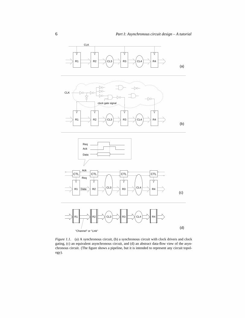
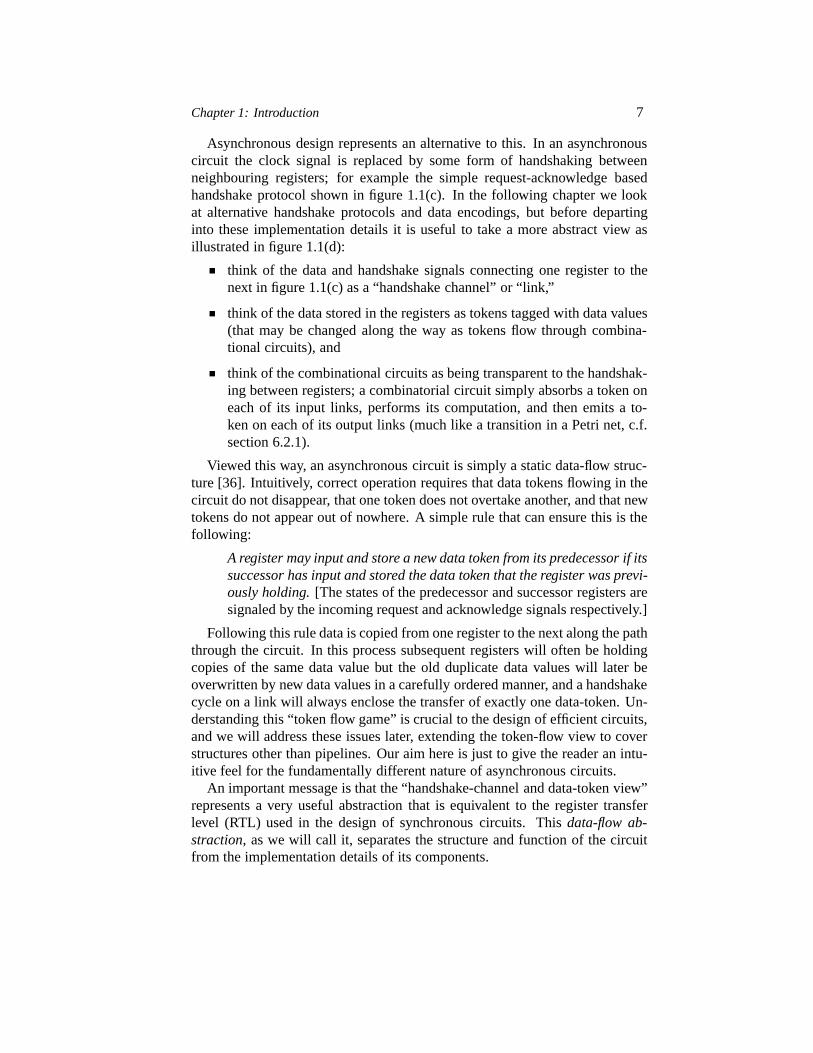
Figure 1.1(a) shows a synchronous circuit. For simplicity the figure shows apipeline, but it is intended to represent any synchronous circuit. When design-ing ASICs using hardware description languages and synthesis tools, designersfocus mostly on the data processing and assume the existence of a global clock.For example, a designer would express the fact that data clocked into registerR3 is a functionCL3 of the data clocked intoR2 at the previous clock as thefollowing assignment of variables:R3 :� CL3�R2�. Figure 1.1(a) representsthis high-level view with a universal clock.
When it comes to physical design, reality is different. Todays ASICs use astructure of clock buffers resulting in a large number of (possibly gated) clocksignals as shown in figure 1.1(b). It is well known that it takes CAD toolsand engineering effort to design the clock gating circuitry and to minimizeand control the skew between the many different clock signals. Guaranteeingthe two-sided timing constraints – the setup to hold time window around theclock edge – in a world that is dominated by wire delays is not an easy task.The buffer-insertion-and-resynthesis process that is used in current commercialCAD tools may not converge and, even if it does, it relies on delay models thatare often of questionable accuracy.
6 Part I: Asynchronous circuit design – A tutorial
CL4
CL4
"Channel" or "Link"
R2 R3 R4R1 CL4CL3
(d)
Ack
R2 R3 R4R1 Data CL3 CL4
ReqCTL CTL CTL CTL
Req
Ack
Data
R2 R3R1 CL3
CLK
(b)
CLK
R2 R3 R4R1 CL3
(a)
(c)
R4
clock gate signal
Figure 1.1. (a) A synchronous circuit, (b) a synchronous circuit with clock drivers and clockgating, (c) an equivalent asynchronous circuit, and (d) an abstract data-flow view of the asyn-chronous circuit. (The figure shows a pipeline, but it is intended to represent any circuit topol-ogy).
Chapter 1: Introduction 7
Asynchronous design represents an alternative to this. In an asynchronouscircuit the clock signal is replaced by some form of handshaking betweenneighbouring registers; for example the simple request-acknowledge basedhandshake protocol shown in figure 1.1(c). In the following chapter we lookat alternative handshake protocols and data encodings, but before departinginto these implementation details it is useful to take a more abstract view asillustrated in figure 1.1(d):
think of the data and handshake signals connecting one register to thenext in figure 1.1(c) as a “handshake channel” or “link,”
think of the data stored in the registers as tokens tagged with data values(that may be changed along the way as tokens flow through combina-tional circuits), and
think of the combinational circuits as being transparent to the handshak-ing between registers; a combinatorial circuit simply absorbs a token oneach of its input links, performs its computation, and then emits a to-ken on each of its output links (much like a transition in a Petri net, c.f.section 6.2.1).
Viewed this way, an asynchronous circuit is simply a static data-flow struc-ture [36]. Intuitively, correct operation requires that data tokens flowing in thecircuit do not disappear, that one token does not overtake another, and that newtokens do not appear out of nowhere. A simple rule that can ensure this is thefollowing:
A register may input and store a new data token from its predecessor if itssuccessor has input and stored the data token that the register was previ-ously holding. [The states of the predecessor and successor registers aresignaled by the incoming request and acknowledge signals respectively.]
Following this rule data is copied from one register to the next along the paththrough the circuit. In this process subsequent registers will often be holdingcopies of the same data value but the old duplicate data values will later beoverwritten by new data values in a carefully ordered manner, and a handshakecycle on a link will always enclose the transfer of exactly one data-token. Un-derstanding this “token flow game” is crucial to the design of efficient circuits,and we will address these issues later, extending the token-flow view to coverstructures other than pipelines. Our aim here is just to give the reader an intu-itive feel for the fundamentally different nature of asynchronous circuits.
An important message is that the “handshake-channel and data-token view”represents a very useful abstraction that is equivalent to the register transferlevel (RTL) used in the design of synchronous circuits. Thisdata-flow ab-straction, as we will call it, separates the structure and function of the circuitfrom the implementation details of its components.
8 Part I: Asynchronous circuit design – A tutorial
Another important message is that it is the handshaking between the regis-ters that controls the flow of tokens, whereas the combinational circuit blocksmust be fully transparent to this handshaking. Ensuring this transparency is notalways trivial; it takes more than a traditional combinational circuit, so we willuse the term ’function block’ to denote a combinational circuit whose inputand output ports are handshake-channels or links.
Finally, some more down-to-earth engineering comments may also be rele-vant. The synchronous circuit in figure 1.1(b) is “controlled” by clock pulsesthat are in phase with a periodic clock signal, whereas the asynchronous circuitin figure 1.1(c) is controlled by locally derived clock pulses that can occur atany time; the local handshaking ensures that clock pulses are generated whereand when needed. This tends to randomize the clock pulses over time, and islikely to result in less electromagnetic emission and a smoother supply currentwithout the largedi�dt spikes that characterize a synchronous circuit.
1.4. Outline of Part I
Chapter 2 presents a number of fundamental concepts and circuits that areimportant for the understanding of the following material. Read through it butdon’t get stuck; you may want to revisit relevant parts later.
Chapters 3 and 4 address asynchronous design at the data-flow level: chap-ter 3 explains the operation of pipelines and rings, introduces a set of hand-shake components and explains how to design (larger) computing structures,and chapter 4 addresses performance analysis and optimization of such struc-tures, both qualitatively and quantitatively.
Chapter 5 addresses the circuit level implementation of the handshake com-ponents introduced in chapter 3, and chapter 6 addresses the design of hazard-free sequential (control) circuits. The latter includes a general introduction tothe topics and in-depth coverage of one specific method: the design of speed-independent control circuits from signal transition graph specifications. Thesetechniques are illustrated by control circuits used in the implementation ofsome of the handshake components introduced in chapter 3.
All of the above chapters 2–6 aim to explain the basic techniques and meth-ods in some depth. The last two chapters are briefer. Chapter 7 introducesmore advanced topics related to the implementation of circuits using the 4-phase bundled-data protocol, and chapter 8 addresses hardware descriptionlanguages and synthesis tools for asynchronous design. Chapter 8 is by nomeans comprehensive; it focuses on CSP-like languages and syntax-directedcompilation, but also describes how asynchronous design can be supported bya standard language, VHDL.
Chapter 2
FUNDAMENTALS
This chapter provides explanations of a number of topics and concepts thatare of fundamental importance for understanding the following chapters andfor appreciating the similarities between the different asynchronous designstyles. The presentation style will be somewhat informal and the aim is toprovide the reader with intuition and insight.
2.1. Handshake protocols
The previous chapter showed one particular handshake protocol known as areturn-to-zero handshake protocol, figure 1.1(c). In the asynchronous commu-nity it is given a more informative name: the 4-phase bundled-data protocol.
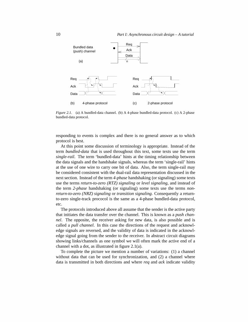
2.1.1 Bundled-data protocols
The termbundled-data refers to a situation where the data signals use nor-mal Boolean levels to encode information, and where separate request andacknowledge wires are bundled with the data signals, figure 2.1(a). In the4-phase protocol illustrated in figure 2.1(b) the request and acknowledge wiresalso use normal Boolean levels to encode information, and the term 4-phaserefers to the number of communication actions: (1) the sender issues data andsets request high, (2) the receiver absorbs the data and sets acknowledge high,(3) the sender responds by taking request low (at which point data is no longerguaranteed to be valid) and (4) the receiver acknowledges this by taking ac-knowledge low. At this point the sender may initiate the next communicationcycle.
The 4-phase bundled data protocol is familiar to most digital designers, butit has a disadvantage in the superfluous return-to-zero transitions that cost un-necessary time and energy. The 2-phase bundled-data protocol shown in fig-ure 2.1(c) avoids this. The information on the request and acknowledge wiresis now encoded as signal transitions on the wires and there is no differencebetween a 0� 1 and a 1� 0 transition, they both represent a “signal event”.Ideally the 2-phase bundled-data protocol should lead to faster circuits thanthe 4-phase bundled-data protocol, but often the implementation of circuits
9
10 Part I: Asynchronous circuit design – A tutorial
(push) channel
(a)
(b) 4-phase protocol (c) 2-phase protocol
Data
Req
Ack
Req
Ack
Data
n
Bundled data
Data
Ack
Req
Figure 2.1. (a) A bundled-data channel. (b) A 4-phase bundled-data protocol. (c) A 2-phasebundled-data protocol.
responding to events is complex and there is no general answer as to whichprotocol is best.
At this point some discussion of terminology is appropriate. Instead of theterm bundled-data that is used throughout this text, some texts use the termsingle-rail. The term ‘bundled-data’ hints at the timing relationship betweenthe data signals and the handshake signals, whereas the term ‘single-rail’ hintsat the use of one wire to carry one bit of data. Also, the term single-rail maybe considered consistent with the dual-rail data representation discussed in thenext section. Instead of the term4-phase handshaking (or signaling) some textsuse the termsreturn-to-zero (RTZ) signaling or level signaling, and instead ofthe term2-phase handshaking (or signaling) some texts use the termsnon-return-to-zero (NRZ) signaling or transition signaling. Consequently a return-to-zero single-track prococol is the same as a 4-phase bundled-data protocol,etc.
The protocols introduced above all assume that the sender is the active partythat initiates the data transfer over the channel. This is known as apush chan-nel. The opposite, the receiver asking for new data, is also possible and iscalled apull channel. In this case the directions of the request and acknowl-edge signals are reversed, and the validity of data is indicated in the acknowl-edge signal going from the sender to the receiver. In abstract circuit diagramsshowing links/channels as one symbol we will often mark the active end of achannel with a dot, as illustrated in figure 2.1(a).
To complete the picture we mention a number of variations: (1) a channelwithout data that can be used for synchronization, and (2) a channel wheredata is transmitted in both directions and wherereq andack indicate validity
Chapter 2: Fundamentals 11
of the data that is exchanged. The latter could be used to interface a read-only memory: the address would be bundled withreq and the data would bebundled withack. These alternatives are explained later in section 7.1.1. In thefollowing sections we will restrict the discussion to push channels.
All the bundled-data protocols rely on delay matching, such that the orderof signal events at the sender’s end is preserved at the receiver’s end. On apush channel, data is valid before request is set high, expressed formally asValid�Data� � Req. This ordering should also be valid at the receiver’s end,and it requires some care when physically implementing such circuits. Possiblesolutions are:
To control the placement and routing of the wires, possibly by routingall signals in a channel as a bundle. This is trivial in a tile-based datapathstructure.
To have a safety margin at the sender’s end.
To insert and/or resize buffers after layout (much as is done in today’ssynthesis and layout CAD tools).
An alternative is to use a more sophisticated protocol that is robust to wiredelays. In the following sections we introduce a number of such protocols thatare completely insensitive to delays.
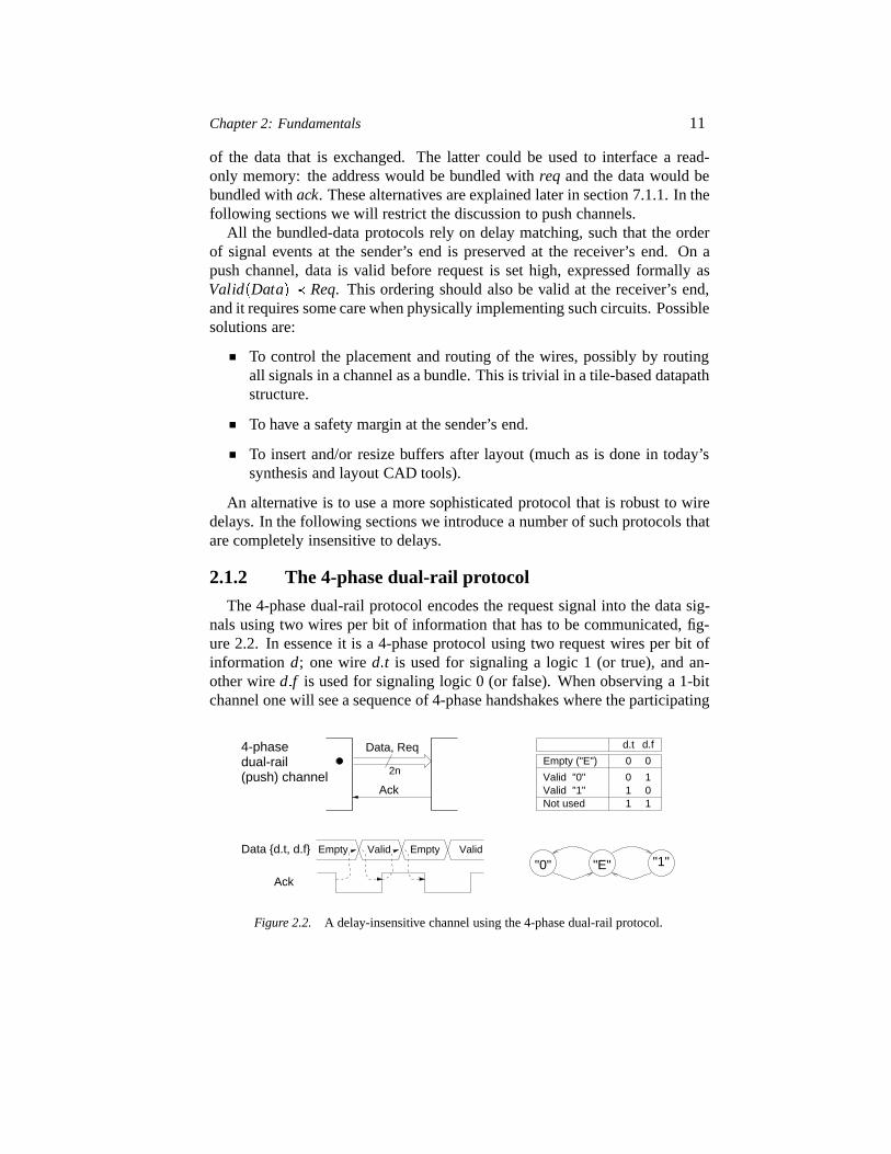
2.1.2 The 4-phase dual-rail protocol
The 4-phase dual-rail protocol encodes the request signal into the data sig-nals using two wires per bit of information that has to be communicated, fig-ure 2.2. In essence it is a 4-phase protocol using two request wires per bit ofinformation d; one wired�t is used for signaling a logic 1 (or true), and an-other wired�f is used for signaling logic 0 (or false). When observing a 1-bitchannel one will see a sequence of 4-phase handshakes where the participating
"1""0" "E"
dual-rail(push) channel
0
011
d.t d.f
0
101
Valid "0"Valid "1"Not used
Empty ("E")2n
Ack
Data, Req4-phase
Data {d.t, d.f} Empty Valid Empty Valid
Ack
Figure 2.2. A delay-insensitive channel using the 4-phase dual-rail protocol.
12 Part I: Asynchronous circuit design – A tutorial
“request” signal in any handshake cycle can be eitherd�t or d�f . This protocolis very robust; two parties can communicate reliably regardless of delays in thewires connecting the two parties – the protocol isdelay-insensitive.
Viewed together the�x�f �x�t� wire pair is a codeword;�x�f �x�t� � �1�0�and�x�f �x�t�� �0�1� represent “valid data” (logic 0 and logic 1 respectively)and�x�f �x�t� � �0�0� represents “no data” (or “spacer” or “empty value” or“NULL”). The codeword�x�f �x�t� � �1�1� is not used, and a transition fromone valid codeword to another valid codeword is not allowed, as illustrated infigure 2.2.
This leads to a more abstract view of 4-phase handshaking: (1) the senderissues a valid codeword, (2) the receiver absorbs the codeword and sets ac-knowledge high, (3) the sender responds by issuing the empty codeword, and(4) the receiver acknowledges this by taking acknowledge low. At this pointthe sender may initiate the next communication cycle. An even more abstractview of what is seen on a channel is a data stream of valid codewords separatedby empty codewords.
Let’s now extend this approach to bit-parallel channels. AnN-bit data chan-nel is formed simply by concatenatingN wire pairs, each using the encodingdescribed above. A receiver is always able to detect when all bits are valid (towhich it responds by taking acknowledge high), and when all bits are empty(to which it responds by taking acknowledge low). This is intuitive, but thereis also some mathematical background – the dual-rail code is a particularlysimple member of the family of delay-insensitive codes [147], and it has somenice properties:
any concatenation of dual-rail codewords is itself a dual-rail codeword.
for a givenN (the number of bits to be communicated), the set of allpossible codewords can bedisjointly divided into 3 sets:
– theempty codeword where allN wire pairs are�0,0�.
– the intermediate codewords where some wire-pairs assume theempty state and some wire pairs assume valid data.
– the 2N differentvalid codewords.
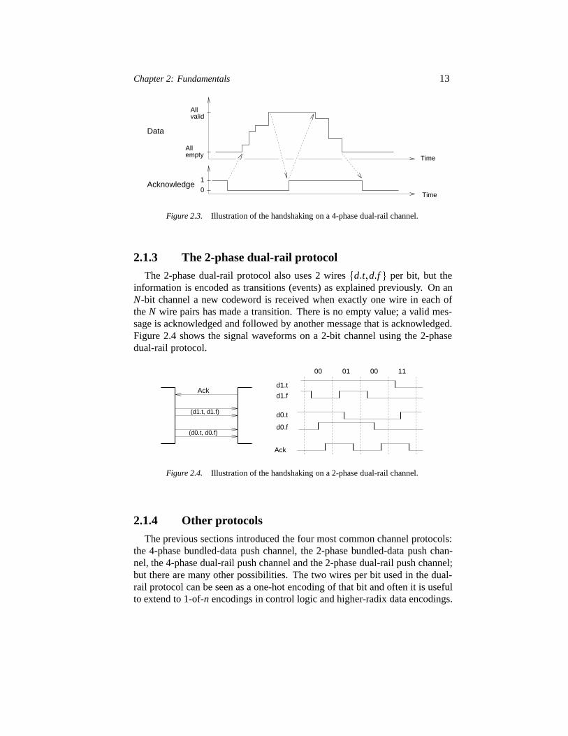
Figure 2.3 illustrates the handshaking on anN-bit channel: a receiver willsee the empty codeword, a sequence of intermediate codewords (as more andmore bits/wire-pairs become valid) and eventually a valid codeword. Afterreceiving and acknowledging the codeword, the receiver will see a sequence ofintermediate codewords (as more and more bits become empty), and eventuallythe empty codeword to which the receiver responds by driving acknowledgelow again.
Chapter 2: Fundamentals 13
Allvalid
Allempty
Acknowledge
Data
Time
1
0
Time
Figure 2.3. Illustration of the handshaking on a 4-phase dual-rail channel.
2.1.3 The 2-phase dual-rail protocol
The 2-phase dual-rail protocol also uses 2 wires�d�t�d�f � per bit, but theinformation is encoded as transitions (events) as explained previously. On anN-bit channel a new codeword is received when exactly one wire in each oftheN wire pairs has made a transition. There is no empty value; a valid mes-sage is acknowledged and followed by another message that is acknowledged.Figure 2.4 shows the signal waveforms on a 2-bit channel using the 2-phasedual-rail protocol.
Ack
(d1.t, d1.f)
(d0.t, d0.f)
d1.t
d1.f
Ack
d0.f
d0.t
00 01 00 11
Figure 2.4. Illustration of the handshaking on a 2-phase dual-rail channel.
2.1.4 Other protocols
The previous sections introduced the four most common channel protocols:the 4-phase bundled-data push channel, the 2-phase bundled-data push chan-nel, the 4-phase dual-rail push channel and the 2-phase dual-rail push channel;but there are many other possibilities. The two wires per bit used in the dual-rail protocol can be seen as a one-hot encoding of that bit and often it is usefulto extend to 1-of-n encodings in control logic and higher-radix data encodings.
14 Part I: Asynchronous circuit design – A tutorial
If the focus is on communication rather than computation,m-of-n encodingsmay be of relevance. The solution space can be expressed as the cross productof a number of options including:
�2-phase�4-phase���bundled-data�dual-rail�1-of-n� � � ����push�pull�
The choice of protocol affects the circuit implementation characteristics(area, speed, power, robustness, etc.). Before continuing with these imple-mentation issues it is necessary to introduce the concept of indication or ac-knowledgement, as well as a new component, the Muller C-element.
2.2. The Muller C-element and the indication principle
In a synchronous circuit the role of the clock is to define points in timewhere signals are stable and valid. In between the clock-ticks, the signalsmay exhibit hazards and may make multiple transitions as the combinationalcircuits stabilize. This does not matter from a functional point of view. Inasynchronous (control) circuits the situation is different. The absence of aclock means that, in many circumstances, signals are required to be valid allthe time, that every signal transition has a meaning and, consequently, thathazards and races must be avoided.
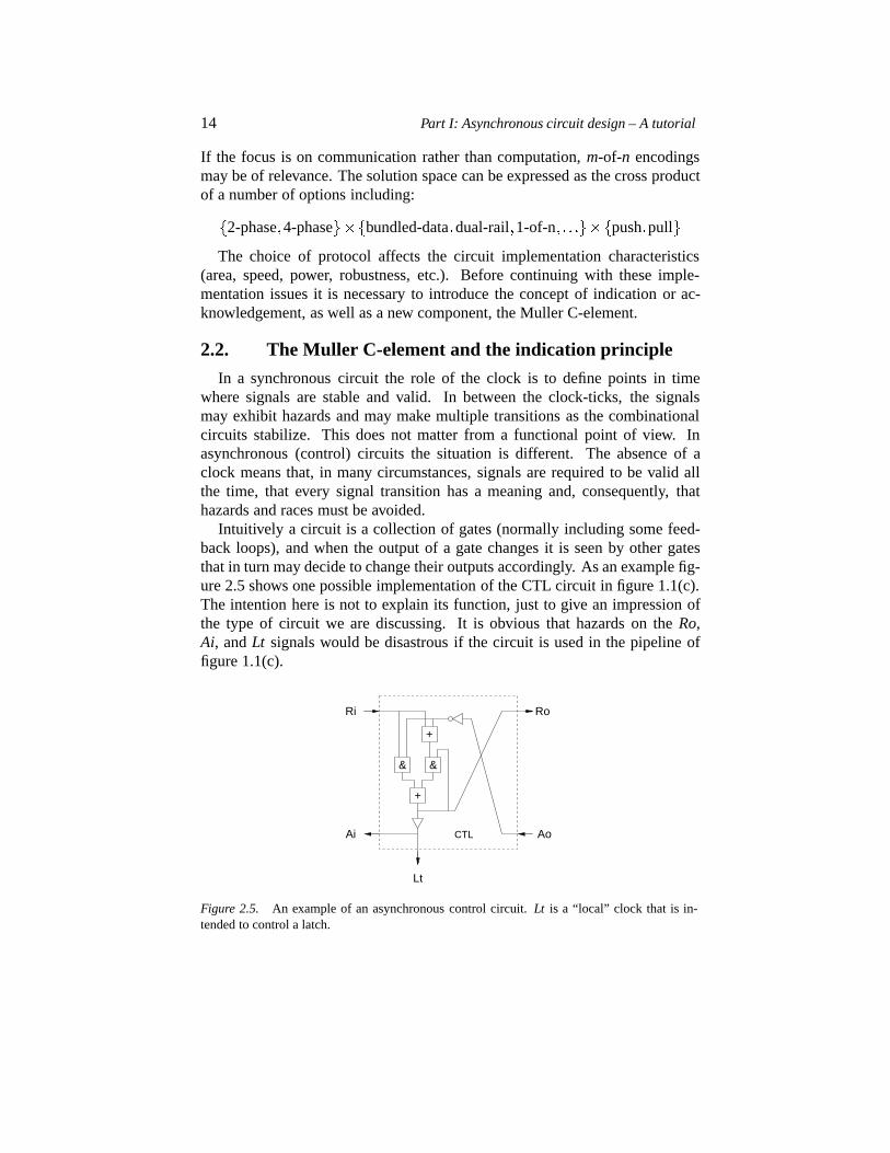
Intuitively a circuit is a collection of gates (normally including some feed-back loops), and when the output of a gate changes it is seen by other gatesthat in turn may decide to change their outputs accordingly. As an example fig-ure 2.5 shows one possible implementation of the CTL circuit in figure 1.1(c).The intention here is not to explain its function, just to give an impression ofthe type of circuit we are discussing. It is obvious that hazards on theRo,Ai, andLt signals would be disastrous if the circuit is used in the pipeline offigure 1.1(c).
+
& &
+
Ao
Ri
Ai
Ro
CTL
Lt
Figure 2.5. An example of an asynchronous control circuit.Lt is a “local” clock that is in-tended to control a latch.
Chapter 2: Fundamentals 15
0011
0
a b y
1
0101
a
b
y+ 1
1
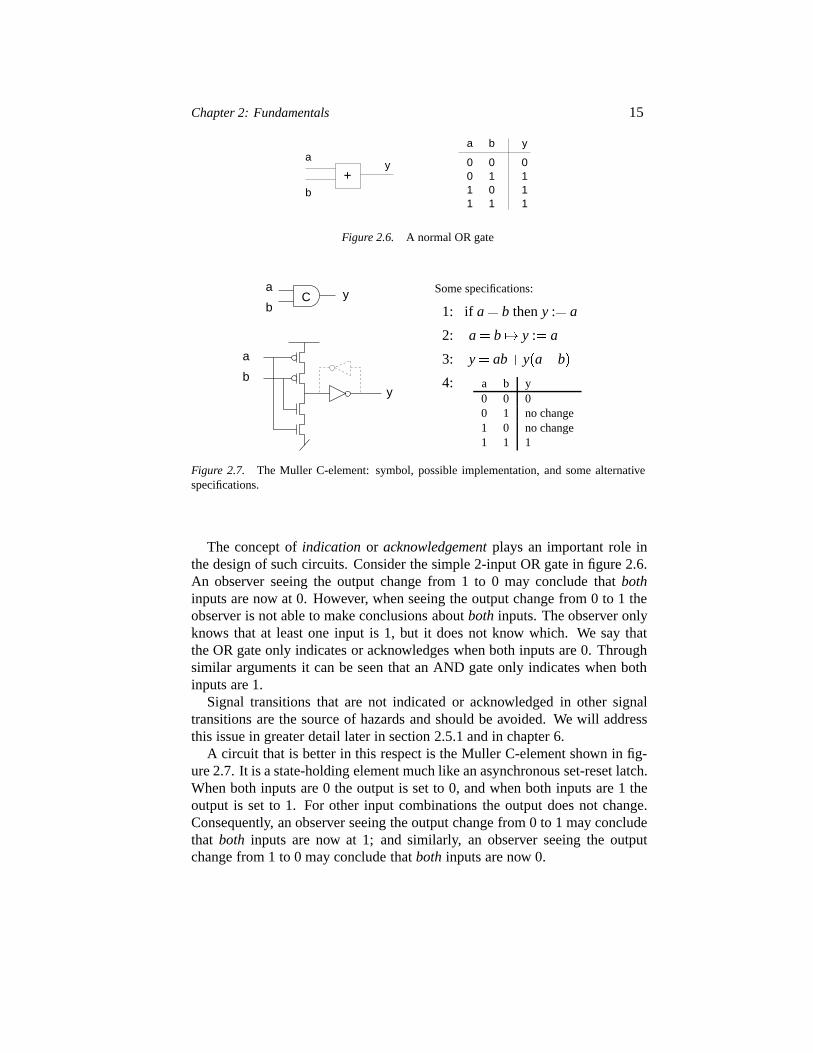
Figure 2.6. A normal OR gate
a
by
ayC
b
Some specifications:
1: if a � b theny :� a
2: a � b �� y :� a
3: y � ab� y�a�b�
4: a b y0 0 00 1 no change1 0 no change1 1 1
Figure 2.7. The Muller C-element: symbol, possible implementation, and some alternativespecifications.
The concept ofindication or acknowledgement plays an important role inthe design of such circuits. Consider the simple 2-input OR gate in figure 2.6.An observer seeing the output change from 1 to 0 may conclude thatbothinputs are now at 0. However, when seeing the output change from 0 to 1 theobserver is not able to make conclusions aboutboth inputs. The observer onlyknows that at least one input is 1, but it does not know which. We say thatthe OR gate only indicates or acknowledges when both inputs are 0. Throughsimilar arguments it can be seen that an AND gate only indicates when bothinputs are 1.
Signal transitions that are not indicated or acknowledged in other signaltransitions are the source of hazards and should be avoided. We will addressthis issue in greater detail later in section 2.5.1 and in chapter 6.
A circuit that is better in this respect is the Muller C-element shown in fig-ure 2.7. It is a state-holding element much like an asynchronous set-reset latch.When both inputs are 0 the output is set to 0, and when both inputs are 1 theoutput is set to 1. For other input combinations the output does not change.Consequently, an observer seeing the output change from 0 to 1 may concludethat both inputs are now at 1; and similarly, an observer seeing the outputchange from 1 to 0 may conclude thatboth inputs are now 0.
16 Part I: Asynchronous circuit design – A tutorial
Combining this with the observation that all asynchronous circuits rely onhandshaking that involves cyclic transitions between 0 and 1, it should be clearthat the Muller C-element is indeed a fundamental component that is exten-sively used in asynchronous circuits.
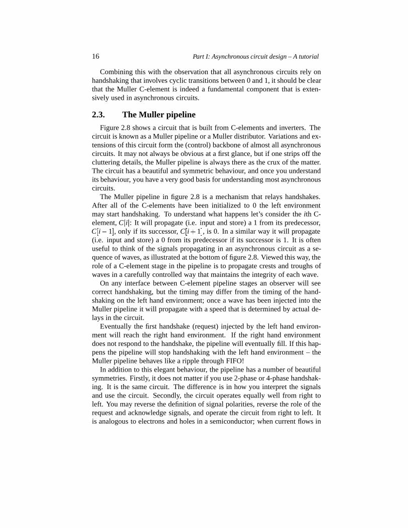
2.3. The Muller pipeline
Figure 2.8 shows a circuit that is built from C-elements and inverters. Thecircuit is known as a Muller pipeline or a Muller distributor. Variations and ex-tensions of this circuit form the (control) backbone of almost all asynchronouscircuits. It may not always be obvious at a first glance, but if one strips off thecluttering details, the Muller pipeline is always there as the crux of the matter.The circuit has a beautiful and symmetric behaviour, and once you understandits behaviour, you have a very good basis for understanding most asynchronouscircuits.
The Muller pipeline in figure 2.8 is a mechanism that relays handshakes.After all of the C-elements have been initialized to 0 the left environmentmay start handshaking. To understand what happens let’s consider theith C-element,C�i�: It will propagate (i.e. input and store) a 1 from its predecessor,C�i�1�, only if its successor,C�i�1�, is 0. In a similar way it will propagate(i.e. input and store) a 0 from its predecessor if its successor is 1. It is oftenuseful to think of the signals propagating in an asynchronous circuit as a se-quence of waves, as illustrated at the bottom of figure 2.8. Viewed this way, therole of a C-element stage in the pipeline is to propagate crests and troughs ofwaves in a carefully controlled way that maintains the integrity of each wave.
On any interface between C-element pipeline stages an observer will seecorrect handshaking, but the timing may differ from the timing of the hand-shaking on the left hand environment; once a wave has been injected into theMuller pipeline it will propagate with a speed that is determined by actual de-lays in the circuit.
Eventually the first handshake (request) injected by the left hand environ-ment will reach the right hand environment. If the right hand environmentdoes not respond to the handshake, the pipeline will eventually fill. If this hap-pens the pipeline will stop handshaking with the left hand environment – theMuller pipeline behaves like a ripple through FIFO!
In addition to this elegant behaviour, the pipeline has a number of beautifulsymmetries. Firstly, it does not matter if you use 2-phase or 4-phase handshak-ing. It is the same circuit. The difference is in how you interpret the signalsand use the circuit. Secondly, the circuit operates equally well from right toleft. You may reverse the definition of signal polarities, reverse the role of therequest and acknowledge signals, and operate the circuit from right to left. Itis analogous to electrons and holes in a semiconductor; when current flows in
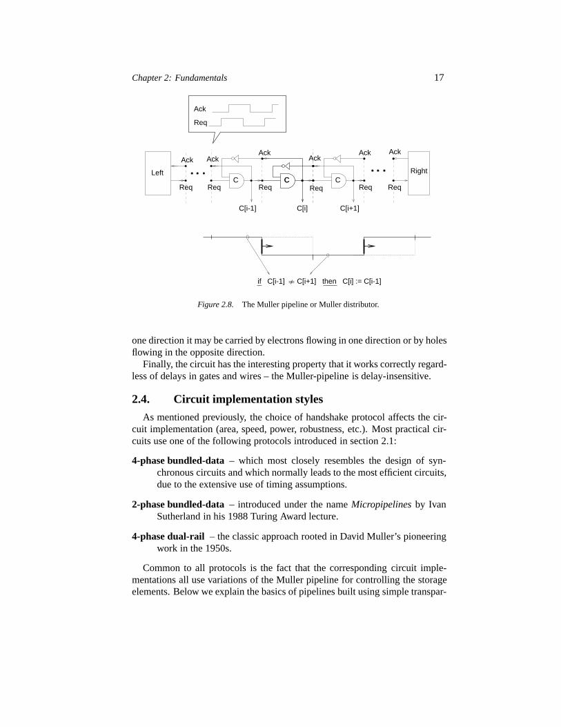
Chapter 2: Fundamentals 17
Req
Ack
Req
Ack
Req
Ack
ReqReq
Ack AckAck
Req Req
Ack
C CC C
if C[i-1] C[i+1] then C[i] := C[i-1]
C[i+1]C[i-1]
Right
C[i]
Left
Figure 2.8. The Muller pipeline or Muller distributor.
one direction it may be carried by electrons flowing in one direction or by holesflowing in the opposite direction.
Finally, the circuit has the interesting property that it works correctly regard-less of delays in gates and wires – the Muller-pipeline is delay-insensitive.
2.4. Circuit implementation styles
As mentioned previously, the choice of handshake protocol affects the cir-cuit implementation (area, speed, power, robustness, etc.). Most practical cir-cuits use one of the following protocols introduced in section 2.1:
4-phase bundled-data– which most closely resembles the design of syn-chronous circuits and which normally leads to the most efficient circuits,due to the extensive use of timing assumptions.
2-phase bundled-data– introduced under the nameMicropipelines by IvanSutherland in his 1988 Turing Award lecture.
4-phase dual-rail – the classic approach rooted in David Muller’s pioneeringwork in the 1950s.
Common to all protocols is the fact that the corresponding circuit imple-mentations all use variations of the Muller pipeline for controlling the storageelements. Below we explain the basics of pipelines built using simple transpar-
18 Part I: Asynchronous circuit design – A tutorial
C C C
CC C
Latch
ENComb.
FLatch
EN
Latch
EN
Req
Ack
Data
Req
Ack
Data
Latch
EN
Latch
EN
Req
Ack
Latch
EN
Req
Ack
Req
Ack
Data
Req
Ack
Data
Req
Ack
Comb.
F
Req
Ack
(a)
(b)
Figure 2.9. A simple 4-phase bundled-data pipeline.
ent latches as storage elements. More optimized and elaborate circuit imple-mentations and more complex circuit structures are the topics of later chapters.
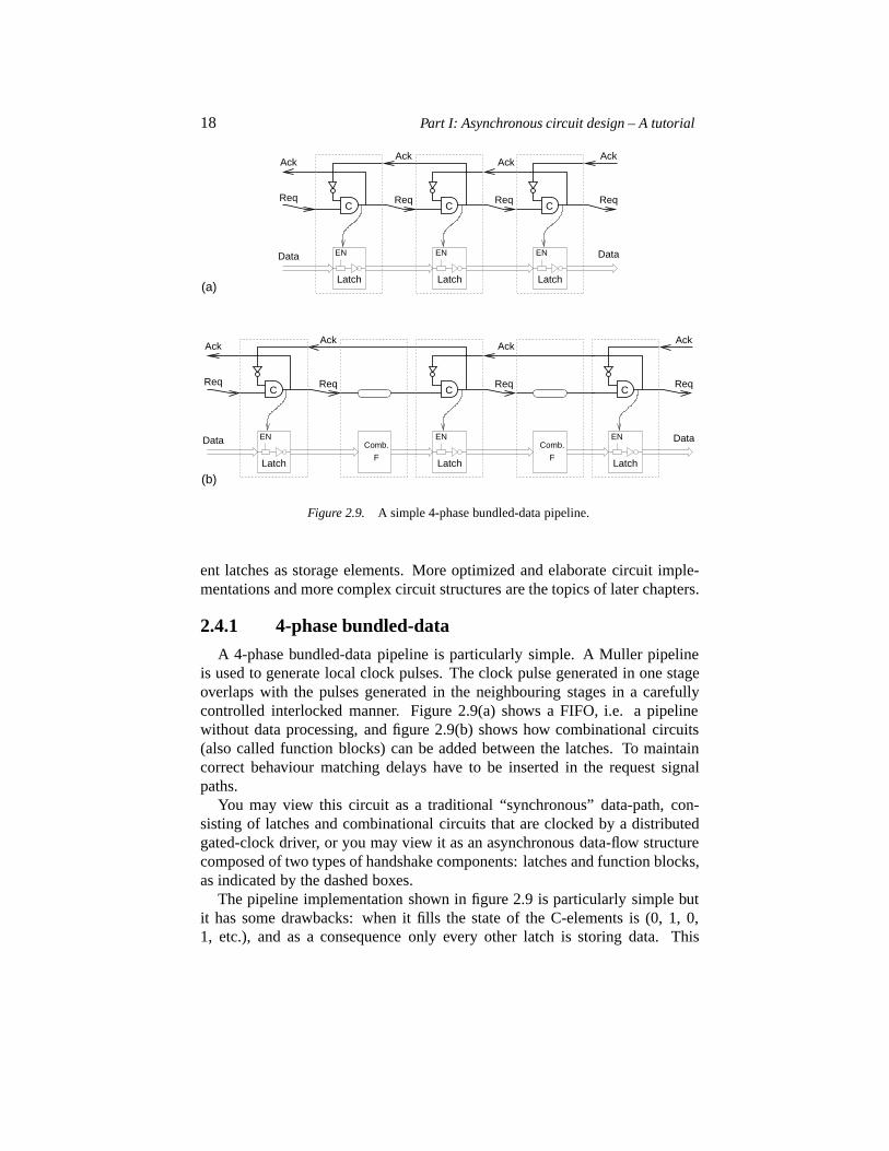
2.4.1 4-phase bundled-data
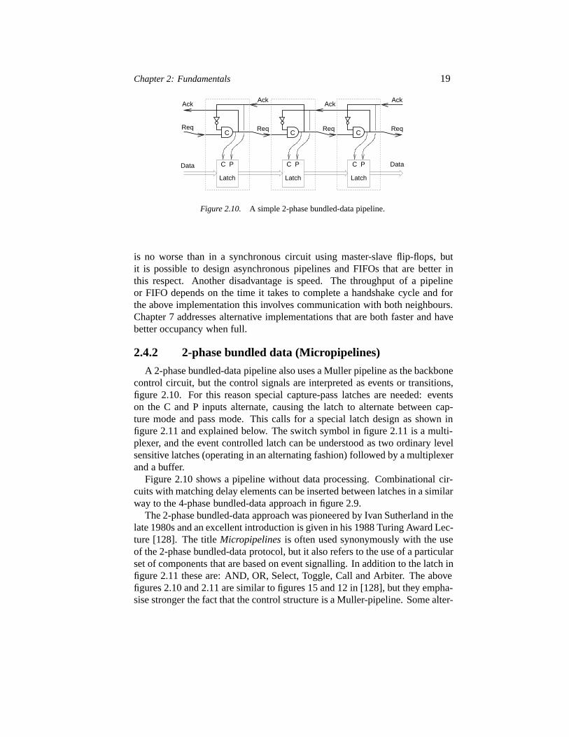
A 4-phase bundled-data pipeline is particularly simple. A Muller pipelineis used to generate local clock pulses. The clock pulse generated in one stageoverlaps with the pulses generated in the neighbouring stages in a carefullycontrolled interlocked manner. Figure 2.9(a) shows a FIFO, i.e. a pipelinewithout data processing, and figure 2.9(b) shows how combinational circuits(also called function blocks) can be added between the latches. To maintaincorrect behaviour matching delays have to be inserted in the request signalpaths.
You may view this circuit as a traditional “synchronous” data-path, con-sisting of latches and combinational circuits that are clocked by a distributedgated-clock driver, or you may view it as an asynchronous data-flow structurecomposed of two types of handshake components: latches and function blocks,as indicated by the dashed boxes.
The pipeline implementation shown in figure 2.9 is particularly simple butit has some drawbacks: when it fills the state of the C-elements is (0, 1, 0,1, etc.), and as a consequence only every other latch is storing data. This
Chapter 2: Fundamentals 19
C CC
C P
Latch
C P
Latch
C P
Latch
Req ReqReq
AckAck
Ack
Req
Ack
DataData
Figure 2.10. A simple 2-phase bundled-data pipeline.
is no worse than in a synchronous circuit using master-slave flip-flops, butit is possible to design asynchronous pipelines and FIFOs that are better inthis respect. Another disadvantage is speed. The throughput of a pipelineor FIFO depends on the time it takes to complete a handshake cycle and forthe above implementation this involves communication with both neighbours.Chapter 7 addresses alternative implementations that are both faster and havebetter occupancy when full.
2.4.2 2-phase bundled data (Micropipelines)
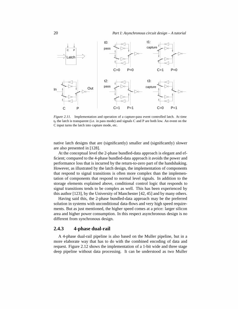
A 2-phase bundled-data pipeline also uses a Muller pipeline as the backbonecontrol circuit, but the control signals are interpreted as events or transitions,figure 2.10. For this reason special capture-pass latches are needed: eventson the C and P inputs alternate, causing the latch to alternate between cap-ture mode and pass mode. This calls for a special latch design as shown infigure 2.11 and explained below. The switch symbol in figure 2.11 is a multi-plexer, and the event controlled latch can be understood as two ordinary levelsensitive latches (operating in an alternating fashion) followed by a multiplexerand a buffer.
Figure 2.10 shows a pipeline without data processing. Combinational cir-cuits with matching delay elements can be inserted between latches in a similarway to the 4-phase bundled-data approach in figure 2.9.
The 2-phase bundled-data approach was pioneered by Ivan Sutherland in thelate 1980s and an excellent introduction is given in his 1988 Turing Award Lec-ture [128]. The titleMicropipelines is often used synonymously with the useof the 2-phase bundled-data protocol, but it also refers to the use of a particularset of components that are based on event signalling. In addition to the latch infigure 2.11 these are: AND, OR, Select, Toggle, Call and Arbiter. The abovefigures 2.10 and 2.11 are similar to figures 15 and 12 in [128], but they empha-sise stronger the fact that the control structure is a Muller-pipeline. Some alter-
20 Part I: Asynchronous circuit design – A tutorial
pass
pass
C P
In Out
C P
C=0 P=0 C=1 P=0
C=1 P=1 C=0 P=1
capture
t0: t1:
capture
t2: t3:
Latch
Figure 2.11. Implementation and operation of a capture-pass event controlled latch. At timet0 the latch is transparent (i.e. in pass mode) and signals C and P are both low. An event on theC input turns the latch into capture mode, etc.
native latch designs that are (significantly) smaller and (significantly) slowerare also presented in [128].
At the conceptual level the 2-phase bundled-data approach is elegant and ef-ficient; compared to the 4-phase bundled-data approach it avoids the power andperformance loss that is incurred by the return-to-zero part of the handshaking.However, as illustrated by the latch design, the implementation of componentsthat respond to signal transitions is often more complex than the implemen-tation of components that respond to normal level signals. In addition to thestorage elements explained above, conditional control logic that responds tosignal transitions tends to be complex as well. This has been experienced bythis author [123], by the University of Manchester [42, 45] and by many others.
Having said this, the 2-phase bundled-data approach may be the preferredsolution in systems with unconditional data-flows and very high speed require-ments. But as just mentioned, the higher speed comes at a price: larger siliconarea and higher power consumption. In this respect asynchronous design is nodifferent from synchronous design.
2.4.3 4-phase dual-rail
A 4-phase dual-rail pipeline is also based on the Muller pipeline, but in amore elaborate way that has to do with the combined encoding of data andrequest. Figure 2.12 shows the implementation of a 1-bit wide and three stagedeep pipeline without data processing. It can be understood as two Muller
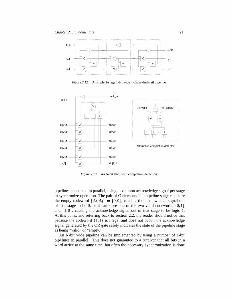
Chapter 2: Fundamentals 21
C
C
+
C
C
+
C
C
+
d.f
d.t
Ack
d.f
d.t
Ack
Figure 2.12. A simple 3-stage 1-bit wide 4-phase dual-rail pipeline.
C
C
C
C
+ + +
C
C
C
di[0].f
di[0].t
di[1].f
di[1].t
di[2].f
di[2].t
+ ++
"All empty"
ack_iack_o
do[0].f
do[0].t
do[1].f
do[1].t
do[2].f
do[2].t
Alternative completion detector
C
"All valid"
& &
Figure 2.13. An N-bit latch with completion detection.
pipelines connected in parallel, using a common acknowledge signal per stageto synchronize operation. The pair of C-elements in a pipeline stage can storethe empty codeword�d�t�d�f � � �0�0�, causing the acknowledge signal outof that stage to be 0, or it can store one of the two valid codewords�0�1�and �1�0�, causing the acknowledge signal out of that stage to be logic 1.At this point, and referring back to section 2.2, the reader should notice thatbecause the codeword�1�1� is illegal and does not occur, the acknowledgesignal generated by the OR gate safely indicates the state of the pipeline stageas being “valid” or “empty.”
An N-bit wide pipeline can be implemented by using a number of 1-bitpipelines in parallel. This does not guarantee to a receiver that all bits in aword arrive at the same time, but often the necessary synchronization is done
22 Part I: Asynchronous circuit design – A tutorial
by
E E 0 0
F FTF
T FTT
110 1
00
NO CHANGE
y.f y.t
01
a b
AND
a
+ y.f
C
C
C
C y.t
a.f00
01
10
11
a.t
b.t
b.f
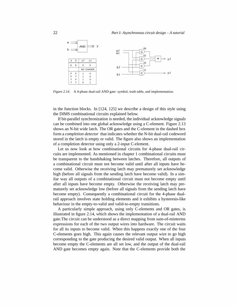
Figure 2.14. A 4-phase dual-rail AND gate: symbol, truth table, and implementation.
in the function blocks. In [124, 125] we describe a design of this style usingthe DIMS combinational circuits explained below.
If bit-parallel synchronization is needed, the individual acknowledge signalscan be combined into one global acknowledge using a C-element. Figure 2.13shows an N-bit wide latch. The OR gates and the C-element in the dashed boxform acompletion detector that indicates whether the N-bit dual-rail codewordstored in the latch is empty or valid. The figure also shows an implementationof a completion detector using only a 2-input C-element.
Let us now look at how combinational circuits for 4-phase dual-rail cir-cuits are implemented. As mentioned in chapter 1 combinational circuits mustbe transparent to the handshaking between latches. Therefore, all outputs ofa combinational circuit must not become valid until after all inputs have be-come valid. Otherwise the receiving latch may prematurely set acknowledgehigh (before all signals from the sending latch have become valid). In a sim-ilar way all outputs of a combinational circuit must not become empty untilafter all inputs have become empty. Otherwise the receiving latch may pre-maturely set acknowledge low (before all signals from the sending latch havebecome empty). Consequently a combinational circuit for the 4-phase dual-rail approach involves state holding elements and it exhibits a hysteresis-likebehaviour in the empty-to-valid and valid-to-empty transitions.
A particularly simple approach, using only C-elements and OR gates, isillustrated in figure 2.14, which shows the implementation of a dual-rail ANDgate.The circuit can be understood as a direct mapping from sum-of-mintermsexpressions for each of the two output wires into hardware. The circuit waitsfor all its inputs to become valid. When this happens exactly one of the fourC-elements goes high. This again causes the relevant output wire to go highcorresponding to the gate producing the desired valid output. When all inputsbecome empty the C-elements are all set low, and the output of the dual-railAND gate becomes empty again. Note that the C-elements provide both the
Chapter 2: Fundamentals 23
necessary ’and’ operator and the hysteresis in the empty-to-valid and valid-to-empty transitions that is required for transparent handshaking. Note also that(again) the OR gate is never exposed to more than one input signal being high.
Other dual-rail gates such as OR and EXOR can be implemented in a sim-ilar fashion, and a dual-rail inverter involves just a swap of the true and falsewires. The transistor count in these basic dual-rail gates is obviously ratherhigh, and in chapter 5 we explore more efficient circuit implementations. Hereour interest is in the fundamental principles.
Given a set of basic dual-rail gates one can construct dual-rail combinationalcircuits for arbitrary Boolean expressions using normal combinational circuitsynthesis techniques. The transparency to handshaking that is a property ofthe basic gates is preserved when composing gates into larger combinationalcircuits.
The fundamental ideas explained above all go back to David Muller’s workin the late 1950s and early 1960s [93, 92]. While [93] develops the fundamen-tal theory for the design of speed-independent circuits, [92] is a more practicalintroduction including a design example: a bit-serial multiplier using latchesand gates as explained above.
2.5. Theory
Asynchronous circuits can be classified, as we will see below, as beingself-timed, speed-independent or delay-insensitive depending on the delay assump-tions that are made. In this section we introduce some important theoreticalconcepts that relate to this classification. The goal is to communicate the basicideas and provide some intuition on the problems and solutions, and a readerwho wishes to dig deeper into the theory is referred to the literature. Somerecent starting points are [95, 54, 69, 35, 18].
2.5.1 The basics of speed-independence
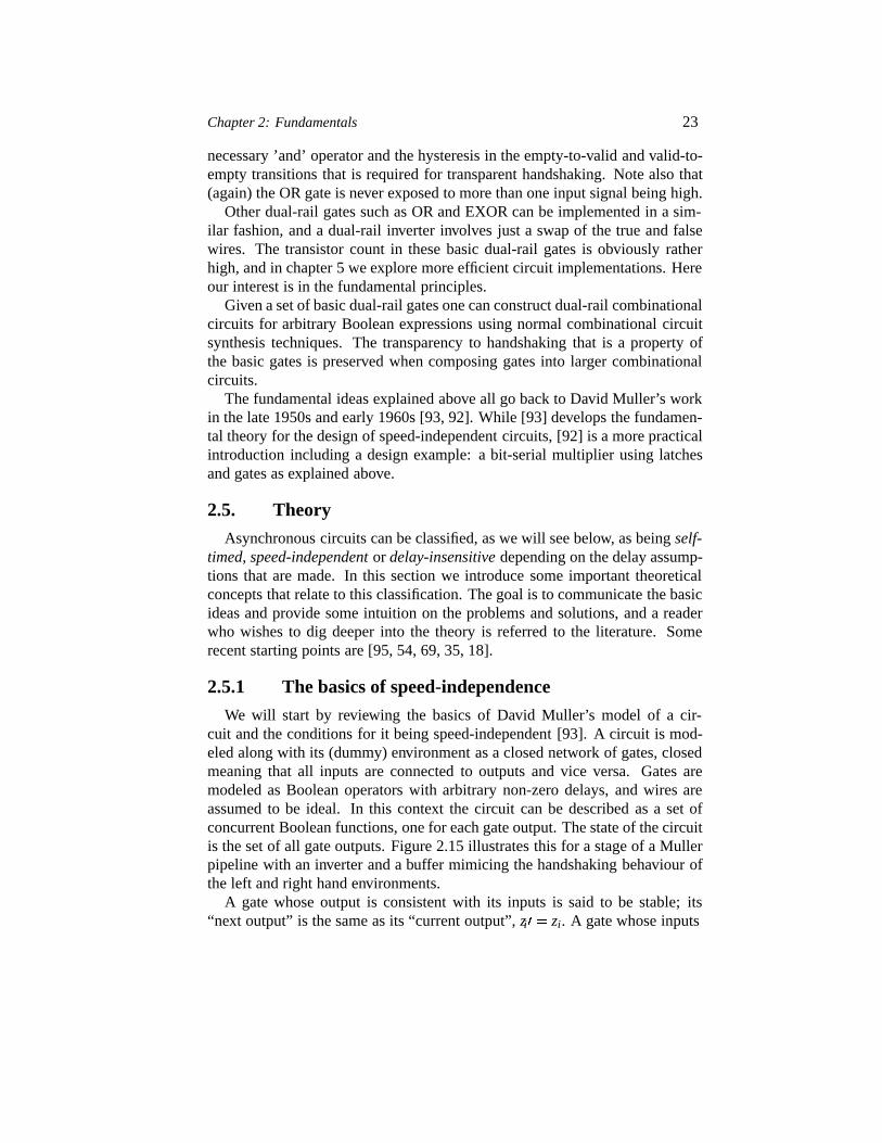
We will start by reviewing the basics of David Muller’s model of a cir-cuit and the conditions for it being speed-independent [93]. A circuit is mod-eled along with its (dummy) environment as a closed network of gates, closedmeaning that all inputs are connected to outputs and vice versa. Gates aremodeled as Boolean operators with arbitrary non-zero delays, and wires areassumed to be ideal. In this context the circuit can be described as a set ofconcurrent Boolean functions, one for each gate output. The state of the circuitis the set of all gate outputs. Figure 2.15 illustrates this for a stage of a Mullerpipeline with an inverter and a buffer mimicing the handshaking behaviour ofthe left and right hand environments.
A gate whose output is consistent with its inputs is said to be stable; its“next output” is the same as its “current output”,zi�� zi. A gate whose inputs
24 Part I: Asynchronous circuit design – A tutorial
r i a i+1
c ia i r i+1
iy
C
ri� � not�ci�
ci� � riyi ��ri � yi�ci
yi� � not�ai�1�
ai�1� � ci
Figure 2.15. Muller model of a Muller pipeline stage with “dummy” gates modeling the envi-ronment behaviour.
have changed in such a way that an output change is called for is said to beexcited; its “next output” is different from its “current output”, i.e.zi� � zi.After an arbitrary delay an excited gate may spontaneously change its outputand become stable. We say that the gate fires, and as excited gates fire andbecome stable with new output values, other gates in turn become excited, etc.
To illustrate this, suppose that the circuit in figure 2.15 is in state�ri�yi�ci�ai�1� � �0�1�0�0�. In this state (the inverter)ri is excited corresponding to theleft environment being about to take request high. After the firing ofri thecircuit reaches state�ri�yi�ci�ai�1� � �1�1�0�0� andci now becomes excited.For synthesis and analysis purposes one can construct the complete state graphrepresenting all possible sequences of gate firings. This is addressed in detailin chapter 6. Here we will restrict the discussion to an explanation of thefundamental ideas.
In the general case it is possible that several gates are excited at the sametime (i.e. in a given state). If one of these gates, sayzi, fires the interestingthing is what happens to the other excited gates which may havezi as oneof their inputs: they may remain excited, or they may find themselves with adifferent set of input signals that no longer calls for an output change.A circuitis speed-independentif the latter never happens. The practical implication ofan excited gate becoming stable without firing is a potential hazard. Sincedelays are unknown the gate may or may not have changed its output, or itmay be in the middle of doing so when the ‘counter-order’ comes calling forthe gate output to remain unchanged.
Since the model involves a Boolean state variable for each gate (and foreach wire segment in the case of delay-insensitive circuits) the state space be-comes very large even for very simple circuits. In chapter 6 we introduce signaltransition graphs as a more abstract representation from which circuits can besynthesized.
Now that we have a model for describing and reasoning about the behaviourof gate-level circuits let’s address the classification of asynchronous circuits.
Chapter 2: Fundamentals 25
d
d
dA
2
3
d1A
BdB
CdC
Figure 2.16. A circuit fragment with gate and wire delays. The output of gate A forks to inputsof gates B and C.
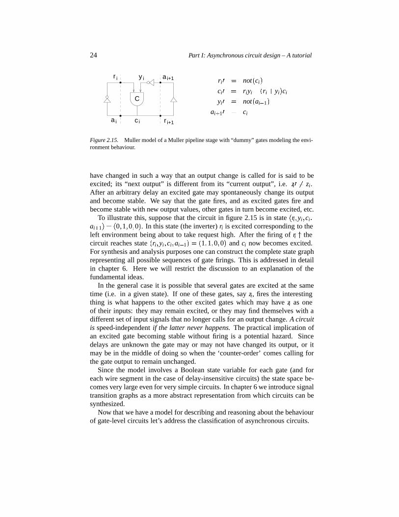
2.5.2 Classification of asynchronous circuits
At the gate level, asynchronous circuits can be classified as being self-timed,speed-independent or delay-insensitive depending on the delay assumptionsthat are made. Figure 2.16 serves to illustrate the following discussion. Thefigure shows three gates: A, B, and C, where the output signal from gate A isconnected to inputs on gates B and C.
A speed-independent (SI) circuit as introduced above is a circuit that oper-ates “correctly” assuming positive, bounded but unknown delays in gates andideal zero-delay wires. Referring to figure 2.16 this means arbitrarydA, dB,anddC, but d1 � d2 � d3 � 0. Assuming ideal zero-delay wires is not veryrealistic in today’s semiconductor processes. By allowing arbitraryd1 andd2
and by requiringd2 � d3 the wire delays can be lumped into the gates, andfrom a theoretical point of view the circuit is still speed-independent.
A circuit that operates “correctly” with positive, bounded but unknown de-lays in wires as well as in gates isdelay-insensitive (DI). Referring to fig-ure 2.16 this means arbitrarydA, dB, dC, d1, d2, andd3. Such circuits are obvi-ously extremely robust. One way to show that a circuit is delay-insensitive is touse a Muller model of the circuit where wire segments (after forks) are modeledas buffer components. If this equivalent circuit model is speed-independent,then the circuit is delay-insensitive.
Unfortunately the class of delay-insensitive circuits is rather small. Onlycircuits composed of C-elements and inverters can be delay-insensitive [82],and the Muller pipeline in figures 2.5, 2.8, and 2.15 is one important example.Circuits that are delay-insensitive with the exception of some carefully identi-fied wire forks whered2 � d3 are calledquasi-delay-insensitive (QDI). Suchwire forks, where signal transitions occur at the same time at all end-points, arecalled isochronic (and discussed in more detail in the next section). Typicallythese isochronic forks are found in gate-level implementations of basic build-ing blocks where the designer can control the wire delays. At the higher levelsof abstraction the composition of building blocks would typically be delay-insensitive. After these comments it is obvious that a distinction between DI,QDI and SI makes good sense.
26 Part I: Asynchronous circuit design – A tutorial
Because the class of delay-insensitive circuits is so small, basically exclud-ing all circuits that compute, most circuits that are referred to in the literatureas delay-insensitive are only quasi-delay-insensitive.
Finally a word aboutself-timed circuits: speed-independence and delay-insensitivity as introduced above are (mathematically) well defined propertiesunder the unbounded gate and wire delay model. Circuits whose correct opera-tion relies on more elaborate and/or engineering timing assumptions are simplycalled self-timed.
2.5.3 Isochronic forks
From the above it is clear that the distinction between speed-independentcircuits and delay-insensitive circuits relates to wire forks and, more specifi-cally, to whether the delays to all end-points of a forking wire are identical ornot. If the delays are identical, the wire-fork is calledisochronic.
The need for isochronic forks is related to the concept of indication intro-duced in section 2.2. Consider a situation in figure 2.16 where gate A haschanged its output. Eventually this change is observed on the inputs of gatesB and C, and after some time gates B and C may respond to the new input byproducing a new output. If this happens we say that the output change on gateA is indicated by output changes on gates B and C. If, on the other hand, onlygate B responds to the new input, it is not possible to establish whether gate Chas seen the input change as well. In this case it is necessary to strengthen theassumptions tod2 � d3 (i.e. that the fork is isochronic) and conclude that sincethe input signal change was indicated by the output of B, gate C has also seenthe change.
2.5.4 Relation to circuits
In the 2-phase and 4-phase bundled-data approaches the control circuits arenormally speed-independent (or in some cases even delay-insensitive), but thedata-path circuits with their matched delays are self-timed. Circuits designedfollowing the 4-phase dual-rail approach are generally quasi-delay-insensitive.In the circuits shown in figures 2.12 and 2.14 the forks that connect to the inputsof several C-elements must be isochronic, whereas the forks that connect to theinputs of several OR gates are delay-insensitive.
The different circuit classes, DI, QDI, SI and self-timed, are not mutually-exclusive ways to build complete systems, but useful abstractions that can beused at different levels of design. In most practical designs they are mixed.For example, in the Amulet processors [44, 43, 48] SI design is used for lo-cal asynchronous controllers, bundled-data for local data processing, and DIis used for high-level composition. Another example is the hearing-aid filterbank design presented in [103]. It uses the DI dual-rail 4-phase protocol inside
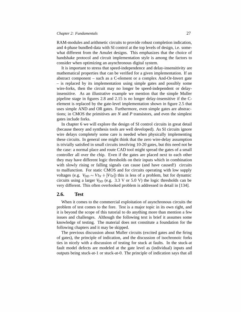
Chapter 2: Fundamentals 27
RAM-modules and arithmetic circuits to provide robust completion indication,and 4-phase bundled-data with SI control at the top levels of design, i.e. some-what different from the Amulet designs. This emphasizes that the choice ofhandshake protocol and circuit implementation style is among the factors toconsider when optimizing an asynchronous digital system.
It is important to stress that speed-independence and delay-insensitivity aremathematical properties that can be verified for a given implementation. If anabstract component – such as a C-element or a complex And-Or-Invert gate– is replaced by its implementation using simple gates and possibly somewire-forks, then the circuit may no longer be speed-independent or delay-insensitive. As an illustrative example we mention that the simple Mullerpipeline stage in figures 2.8 and 2.15 is no longer delay-insensitive if the C-element is replaced by the gate-level implementation shown in figure 2.5 thatuses simple AND and OR gates. Furthermore, even simple gates are abstrac-tions; in CMOS the primitives areN andP transistors, and even the simplestgates include forks.
In chapter 6 we will explore the design of SI control circuits in great detail(because theory and synthesis tools are well developed). As SI circuits ignorewire delays completely some care is needed when physically implementingthese circuits. In general one might think that the zero wire-delay assumptionis trivially satisfied in small circuits involving 10-20 gates, but this need not bethe case: a normal place and route CAD tool might spread the gates of a smallcontroller all over the chip. Even if the gates are placed next to each otherthey may have different logic thresholds on their inputs which in combinationwith slowly rising or falling signals can cause (and have caused!) circuitsto malfunction. For static CMOS and for circuits operating with low supplyvoltages (e.g.VDD � VtN � �VtP�) this is less of a problem, but for dynamiccircuits using a largerVDD (e.g. 3.3 V or 5.0 V) the logic thresholds can bevery different. This often overlooked problem is addressed in detail in [134].
2.6. Test
When it comes to the commercial exploitation of asynchronous circuits theproblem of test comes to the fore. Test is a major topic in its own right, andit is beyond the scope of this tutorial to do anything more than mention a fewissues and challenges. Although the following text is brief it assumes someknowledge of testing. The material does not constitute a foundation for thefollowing chapters and it may be skipped.
The previous discussion about Muller circuits (excited gates and the firingof gates), the principle of indication, and the discussion of isochronoic forksties in nicely with a discussion of testing for stuck at faults. In the stuck-atfault model defects are modeled at the gate level as (individual) inputs andoutputs being stuck-at-1 or stuck-at-0. The principle of indication says that all
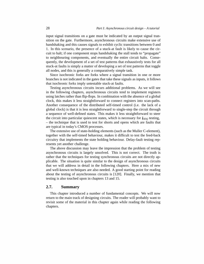
28 Part I: Asynchronous circuit design – A tutorial
input signal transitions on a gate must be indicated by an output signal tran-sition on the gate. Furthermore, asynchronous circuits make extensive use ofhandshaking and this causes signals to exhibit cyclic transitions between 0 and1. In this scenario, the presence of a stuck-at fault is likely to cause the cir-cuit to halt; if one component stops handshaking the stall tends to “propagate”to neighbouring components, and eventually the entire circuit halts. Conse-quently, the development of a set of test patterns that exhaustively tests for allstuck-at faults is simply a matter of developing a set of test patterns that toggleall nodes, and this is generally a comparatively simple task.
Since isochronic forks are forks where a signal transition in one or morebranches is not indicated in the gates that take these signals as inputs, it followsthat isochronic forks imply untestable stuck-at faults.
Testing asynchronous circuits incurs additional problems. As we will seein the following chapters, asynchronous circuits tend to implement registersusing latches rather than flip-flops. In combination with the absence of a globalclock, this makes it less straightforward to connect registers into scan-paths.Another consequence of the distributed self-timed control (i.e. the lack of aglobal clock) is that it is less straightforward to single-step the circuit througha sequence of well-defined states. This makes it less straightforward to steerthe circuit into particular quiescent states, which is necessary forIDDQ testing,– the technique that is used to test for shorts and opens which are faults thatare typical in today’s CMOS processes.
The extensive use of state-holding elements (such as the Muller C-element),together with the self-timed behaviour, makes it difficult to test the feed-backcircuitry that implements the state holding behaviour. Delay-fault testing rep-resents yet another challenge.
The above discussion may leave the impression that the problem of testingasynchronous circuits is largely unsolved. This is not correct. The truth israther that the techniques for testing synchronous circuits are not directly ap-plicable. The situation is quite similar to the design of asynchronous circuitsthat we will address in detail in the following chapters. Here a mix of newand well-known techniques are also needed. A good starting point for readingabout the testing of asynchronous circuits is [120]. Finally, we mention thattesting is also touched upon in chapters 13 and 15.
2.7. Summary
This chapter introduced a number of fundamental concepts. We will nowreturn to the main track of designing circuits. The reader will probably want torevisit some of the material in this chapter again while reading the followingchapters.
Chapter 3
STATIC DATA-FLOW STRUCTURES
In this chapter we will develop a high-level view of asynchronous designthat is equivalent to RTL (register transfer level) in synchronous design. Atthis level the circuits may be viewed as static data-flow structures. The aim isto focus on the behaviour of the circuits, and to abstract away the details of thehandshake signaling which can be considered an orthogonal implementationissue.
3.1. Introduction
The various handshake protocols and the associated circuit implementa-tion styles presented in the previous chapters are rather different. However,when looking at the circuits at a more abstract level – the data-flow handshake-channel level introduced in chapter 1 – these differences diminish, and it makesgood sense to view the choice of handshake protocol and circuit implementa-tion style as low level implementation decisions that can be made largely in-dependently from the more abstract design decisions that establish the overallstructure and operation of the circuit.
Throughout this chapter we will assume a 4-phase protocol since this ismost common. From a data-flow point of view this means that the we will bedealing with data streams composed of alternating valid and empty values – ina two-phase protocol we would see only a sequence of valid values, but apartfrom that everything else would be the same. Furthermore we will be dealingwith simple latches as storage elements. The latches are controlled accordingto the simple rule stated in chapter 1:
A latch may input and store a new token (valid or empty) from its pre-decessor if its successor latch has input and stored the token that it waspreviously holding.
Latches are the only components that initiate and take an active part in hand-shaking; all other components are “transparent” to the handshaking. To easethe distinction between latches and combinational circuits and to emphasizethe token flow in circuit diagrams, we will use a box symbol with double verti-cal lines to represent latches throughout the rest of this tutorial (see figure 3.1).
29
30 Part I: Asynchronous circuit design – A tutorial
L0 L1 L2 L3 L4
E V V E E
Bubble BubbleToken Token Token
Figure 3.1. A possible state of a five stage pipeline.
V
V E V
E E
EVV
E V Et3:
t2:
t1:
t0: Token Token Bubble
Figure 3.2. Ring: (a) a possible state; and (b) a sequence of data transfers.
3.2. Pipelines and rings
Figure 3.1 shows a snapshot of a pipeline composed of five latches. The“box arrows” represent channels or links consisting of request, acknowledgeand data signals (as explained on page 5). The valid value in L1 has justbeen copied into L2 and the empty value in L3 has just been copied intoL4. This means that L1 and L3 are now holding old duplicates of the val-ues now stored in L2 and L4. Such old duplicates are called “bubbles”, and thenewest/rightmost valid and empty values are called “tokens”. To distinguishtokens from bubbles, tokens are represented with a circle around the value. Inthis way a latch may hold a valid token, an empty token or a bubble. Bubblescan be viewed as catalysts: a bubble allows a token to move forward, and insupporting this the bubble moves backwards one step.
Any circuit should have one or more bubbles, otherwise it will be in a dead-lock state. This is a matter of initializing the circuit properly, and we willelaborate on this shortly. Furthermore, as we will see later, the number ofbubbles also has a significant impact on performance.
In a pipeline with at least three latches, it is possible to connect the outputof the last stage to the input of the first, forming a ring in which data tokenscan circulate autonomously. Assuming the ring is initialized as shown in fig-ure 3.2(a) at timet0 with a valid token, an empty token and a bubble, the firststeps of the circulation process are shown in figure 3.2(b), at timest1, t2 and
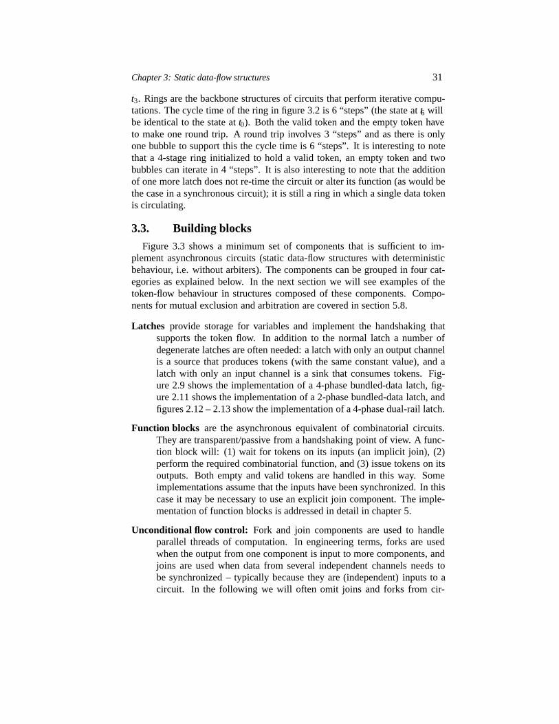
Chapter 3: Static data-flow structures 31
t3. Rings are the backbone structures of circuits that perform iterative compu-tations. The cycle time of the ring in figure 3.2 is 6 “steps” (the state att6 willbe identical to the state att0). Both the valid token and the empty token haveto make one round trip. A round trip involves 3 “steps” and as there is onlyone bubble to support this the cycle time is 6 “steps”. It is interesting to notethat a 4-stage ring initialized to hold a valid token, an empty token and twobubbles can iterate in 4 “steps”. It is also interesting to note that the additionof one more latch does not re-time the circuit or alter its function (as would bethe case in a synchronous circuit); it is still a ring in which a single data tokenis circulating.
3.3. Building blocks
Figure 3.3 shows a minimum set of components that is sufficient to im-plement asynchronous circuits (static data-flow structures with deterministicbehaviour, i.e. without arbiters). The components can be grouped in four cat-egories as explained below. In the next section we will see examples of thetoken-flow behaviour in structures composed of these components. Compo-nents for mutual exclusion and arbitration are covered in section 5.8.
Latches provide storage for variables and implement the handshaking thatsupports the token flow. In addition to the normal latch a number ofdegenerate latches are often needed: a latch with only an output channelis a source that produces tokens (with the same constant value), and alatch with only an input channel is a sink that consumes tokens. Fig-ure 2.9 shows the implementation of a 4-phase bundled-data latch, fig-ure 2.11 shows the implementation of a 2-phase bundled-data latch, andfigures 2.12 – 2.13 show the implementation of a 4-phase dual-rail latch.
Function blocks are the asynchronous equivalent of combinatorial circuits.They are transparent/passive from a handshaking point of view. A func-tion block will: (1) wait for tokens on its inputs (an implicit join), (2)perform the required combinatorial function, and (3) issue tokens on itsoutputs. Both empty and valid tokens are handled in this way. Someimplementations assume that the inputs have been synchronized. In thiscase it may be necessary to use an explicit join component. The imple-mentation of function blocks is addressed in detail in chapter 5.
Unconditional flow control: Fork and join components are used to handleparallel threads of computation. In engineering terms, forks are usedwhen the output from one component is input to more components, andjoins are used when data from several independent channels needs tobe synchronized – typically because they are (independent) inputs to acircuit. In the following we will often omit joins and forks from cir-
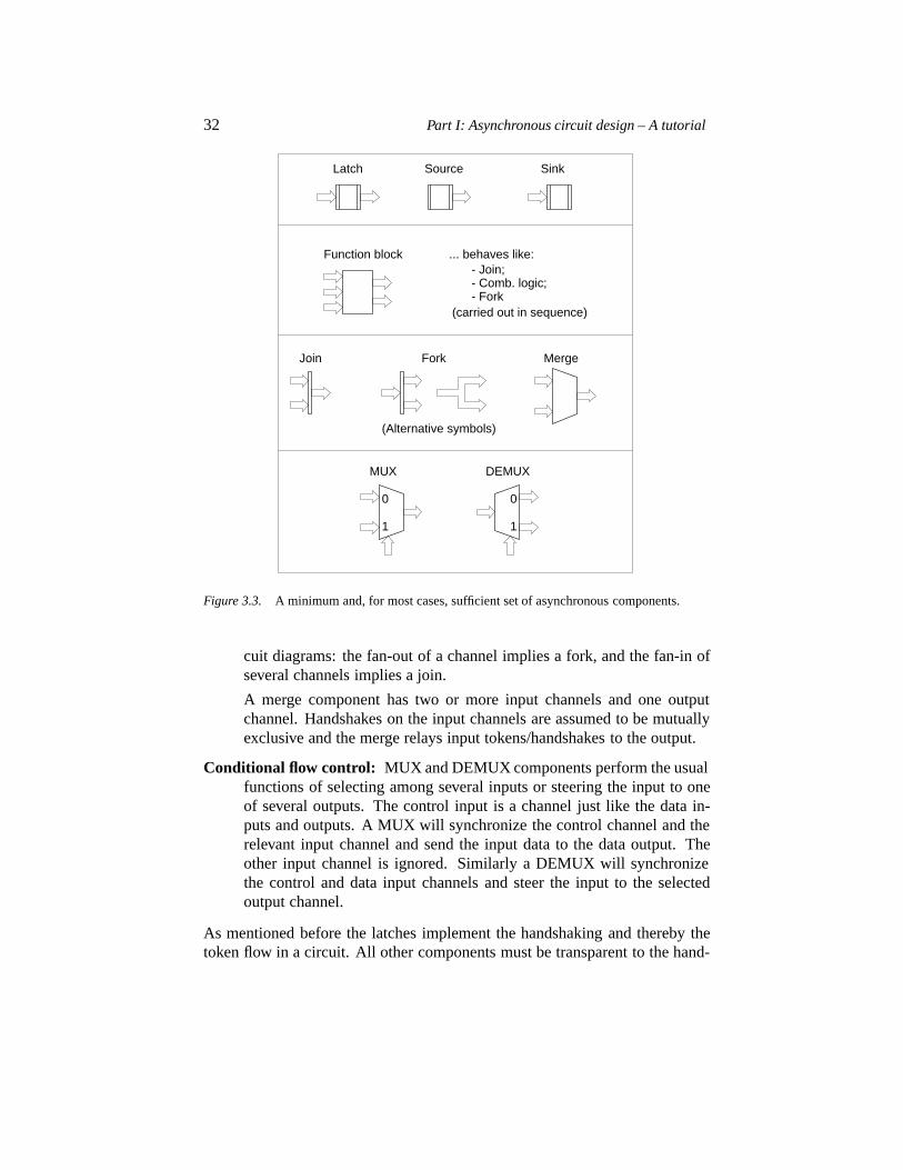
32 Part I: Asynchronous circuit design – A tutorial
Merge
Latch Source Sink
0
1
MUX DEMUX
0
1
Function block
Join
... behaves like:
Fork
- Fork(carried out in sequence)
- Join; - Comb. logic;
(Alternative symbols)
Figure 3.3. A minimum and, for most cases, sufficient set of asynchronous components.
cuit diagrams: the fan-out of a channel implies a fork, and the fan-in ofseveral channels implies a join.
A merge component has two or more input channels and one outputchannel. Handshakes on the input channels are assumed to be mutuallyexclusive and the merge relays input tokens/handshakes to the output.
Conditional flow control: MUX and DEMUX components perform the usualfunctions of selecting among several inputs or steering the input to oneof several outputs. The control input is a channel just like the data in-puts and outputs. A MUX will synchronize the control channel and therelevant input channel and send the input data to the data output. Theother input channel is ignored. Similarly a DEMUX will synchronizethe control and data input channels and steer the input to the selectedoutput channel.
As mentioned before the latches implement the handshaking and thereby thetoken flow in a circuit. All other components must be transparent to the hand-
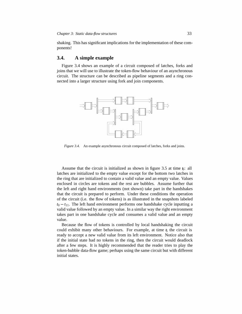
Chapter 3: Static data-flow structures 33
shaking. This has significant implications for the implementation of these com-ponents!
3.4. A simple example
Figure 3.4 shows an example of a circuit composed of latches, forks andjoins that we will use to illustrate the token-flow behaviour of an asynchronouscircuit. The structure can be described as pipeline segments and a ring con-nected into a larger structure using fork and join components.
Figure 3.4. An example asynchronous circuit composed of latches, forks and joins.
Assume that the circuit is initialized as shown in figure 3.5 at timet0: alllatches are initialized to the empty value except for the bottom two latches inthe ring that are initialized to contain a valid value and an empty value. Valuesenclosed in circles are tokens and the rest are bubbles. Assume further thatthe left and right hand environments (not shown) take part in the handshakesthat the circuit is prepared to perform. Under these conditions the operationof the circuit (i.e. the flow of tokens) is as illustrated in the snapshots labeledt0� t11. The left hand environment performs one handshake cycle inputting avalid value followed by an empty value. In a similar way the right environmenttakes part in one handshake cycle and consumes a valid value and an emptyvalue.
Because the flow of tokens is controlled by local handshaking the circuitcould exhibit many other behaviours. For example, at timet5 the circuit isready to accept a new valid value from its left environment. Notice also thatif the initial state had no tokens in the ring, then the circuit would deadlockafter a few steps. It is highly recommended that the reader tries to play thetoken-bubble data-flow game; perhaps using the same circuit but with differentinitial states.
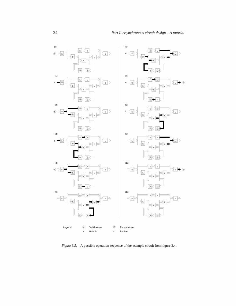
34 Part I: Asynchronous circuit design – A tutorial
V
V
V
V
V
V
V
E
V
E
E
E
E
V
E
E
V
VE
E
V
E
E V
V
VE
E
V
E
V
E
V
E
V
E
EV
E
E
V E
V E
E
V E
V E
E
E
E
E
EE
E
V
E
E
E E
E
E
E
E
E
E
V
V
E
E
V
V
E
E
E
E
E
t0:
t1:
t2:
t3:
E E
V
t5:
t4:
E
E
V
V
V
V
V
E
E
t6:
E E
t7:
E
t8:
E
EE
E
E
V
E
E
E
E
E
E
E
t9:
E
E
E E
E
E
E
E
E
E E
E
E
E
t10:
t10:
V Bubble E
Valid token Empty token
Bubble
Legend:
Figure 3.5. A possible operation sequence of the example circuit from figure 3.4.
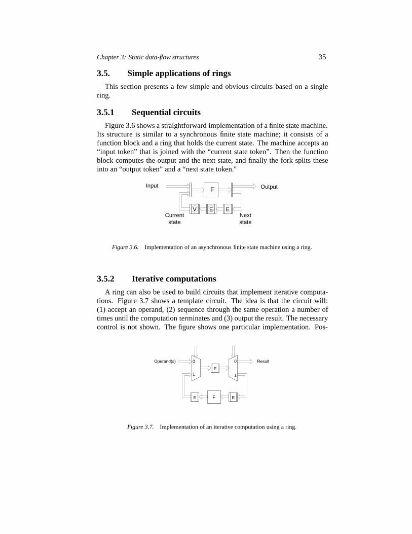
Chapter 3: Static data-flow structures 35
3.5. Simple applications of rings
This section presents a few simple and obvious circuits based on a singlering.
3.5.1 Sequential circuits
Figure 3.6 shows a straightforward implementation of a finite state machine.Its structure is similar to a synchronous finite state machine; it consists of afunction block and a ring that holds the current state. The machine accepts an“input token” that is joined with the “current state token”. Then the functionblock computes the output and the next state, and finally the fork splits theseinto an “output token” and a “next state token.”
stateCurrent Next
state
FInput Output
V E E
Figure 3.6. Implementation of an asynchronous finite state machine using a ring.
3.5.2 Iterative computations
A ring can also be used to build circuits that implement iterative computa-tions. Figure 3.7 shows a template circuit. The idea is that the circuit will:(1) accept an operand, (2) sequence through the same operation a number oftimes until the computation terminates and (3) output the result. The necessarycontrol is not shown. The figure shows one particular implementation. Pos-
FE E
1
0 0
1
Operand(s) Result
E
Figure 3.7. Implementation of an iterative computation using a ring.
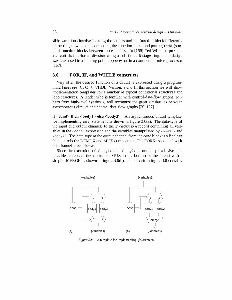
36 Part I: Asynchronous circuit design – A tutorial
sible variations involve locating the latches and the function block differentlyin the ring as well as decomposing the function block and putting these (sim-pler) function blocks between more latches. In [156] Ted Williams presentsa circuit that performs division using a self-timed 5-stage ring. This designwas later used in a floating point coprocessor in a commercial microprocessor[157].
3.6. FOR, IF, and WHILE constructs
Very often the desired function of a circuit is expressed using a program-ming language (C, C++, VHDL, Verilog, etc.). In this section we will showimplementation templates for a number of typical conditional structures andloop structures. A reader who is familiar with control-data-flow graphs, per-haps from high-level synthesis, will recognize the great similarities betweenasynchronous circuits and control-data-flow graphs [36, 127].
if <cond> then <body1> else <body2> An asynchronous circuit templatefor implementing anif statement is shown in figure 3.8(a). The data-type ofthe input and output channels to theif circuit is a record containing all vari-ables in the<cond> expression and the variables manipulated by<body1> and<body2>. The data-type of the output channel from the cond block is a Booleanthat controls the DEMUX and MUX components. The FORK associated withthis channel is not shown.
Since the execution of<body1> and <body2> is mutually exclusive it ispossible to replace the controlled MUX in the bottom of the circuit with asimpler MERGE as shown in figure 3.8(b). The circuit in figure 3.8 contains
body1 body2
10
10
{variables}
cond
{variables}
body1 body2
10
{variables}
cond
{variables}
merge
(b)(a)
Figure 3.8. A template for implementingif statements.
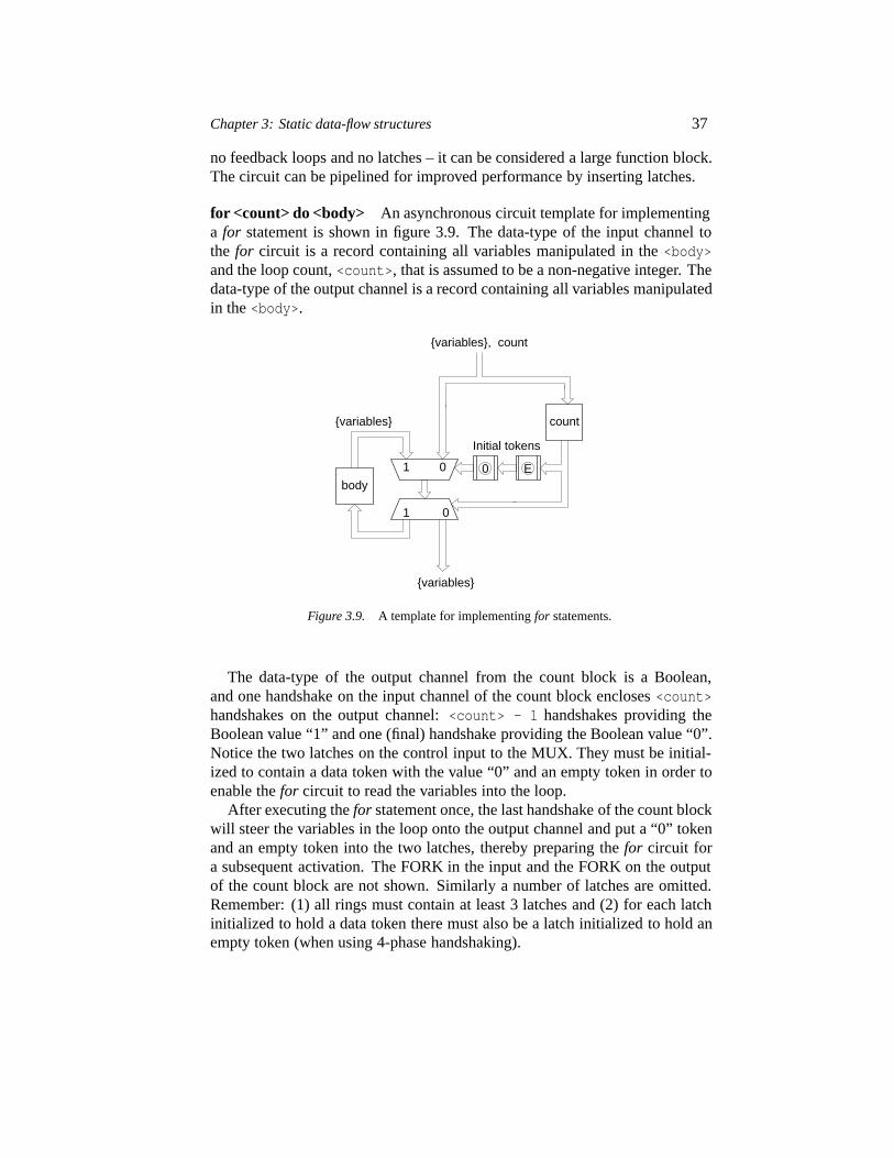
Chapter 3: Static data-flow structures 37
no feedback loops and no latches – it can be considered a large function block.The circuit can be pipelined for improved performance by inserting latches.
for <count> do <body> An asynchronous circuit template for implementinga for statement is shown in figure 3.9. The data-type of the input channel tothe for circuit is a record containing all variables manipulated in the<body>and the loop count,<count>, that is assumed to be a non-negative integer. Thedata-type of the output channel is a record containing all variables manipulatedin the<body>.
0
count
Ebody
1 0
{variables}
{variables}
{variables}, count
1 0
Initial tokens
Figure 3.9. A template for implementingfor statements.
The data-type of the output channel from the count block is a Boolean,and one handshake on the input channel of the count block encloses<count>handshakes on the output channel:<count> - 1 handshakes providing theBoolean value “1” and one (final) handshake providing the Boolean value “0”.Notice the two latches on the control input to the MUX. They must be initial-ized to contain a data token with the value “0” and an empty token in order toenable thefor circuit to read the variables into the loop.
After executing thefor statement once, the last handshake of the count blockwill steer the variables in the loop onto the output channel and put a “0” tokenand an empty token into the two latches, thereby preparing thefor circuit fora subsequent activation. The FORK in the input and the FORK on the outputof the count block are not shown. Similarly a number of latches are omitted.Remember: (1) all rings must contain at least 3 latches and (2) for each latchinitialized to hold a data token there must also be a latch initialized to hold anempty token (when using 4-phase handshaking).
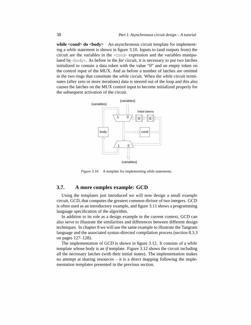
38 Part I: Asynchronous circuit design – A tutorial
while <cond> do <body> An asynchronous circuit template for implement-ing awhile statement is shown in figure 3.10. Inputs to (and outputs from) thecircuit are the variables in the<cond> expression and the variables manipu-lated by<body>. As before in thefor circuit, it is necessary to put two latchesinitialized to contain a data token with the value “0” and an empty token onthe control input of the MUX. And as before a number of latches are omittedin the two rings that constitute thewhile circuit. When thewhile circuit termi-nates (after zero or more iterations) data is steered out of the loop and this alsocauses the latches on the MUX control input to become initialized properly forthe subsequent activation of the circuit.
0
cond
{variables}
body
{variables}
{variables}
1 0
1 0
E
Initial tokens
Figure 3.10. A template for implementingwhile statements.
3.7. A more complex example: GCD
Using the templates just introduced we will now design a small examplecircuit, GCD, that computes the greatest common divisor of two integers. GCDis often used as an introductory example, and figure 3.11 shows a programminglanguage specification of the algorithm.
In addition to its role as a design example in the current context, GCD canalso serve to illustrate the similarities and differences between different designtechniques. In chapter 8 we will use the same example to illustrate the Tangramlanguage and the associated syntax-directed compilation process (section 8.3.3on pages 127–128).
The implementation of GCD is shown in figure 3.12. It consists of awhiletemplate whose body is anif template. Figure 3.12 shows the circuit includingall the necessary latches (with their initial states). The implementation makesno attempt at sharing resources – it is a direct mapping following the imple-mentation templates presented in the previous section.
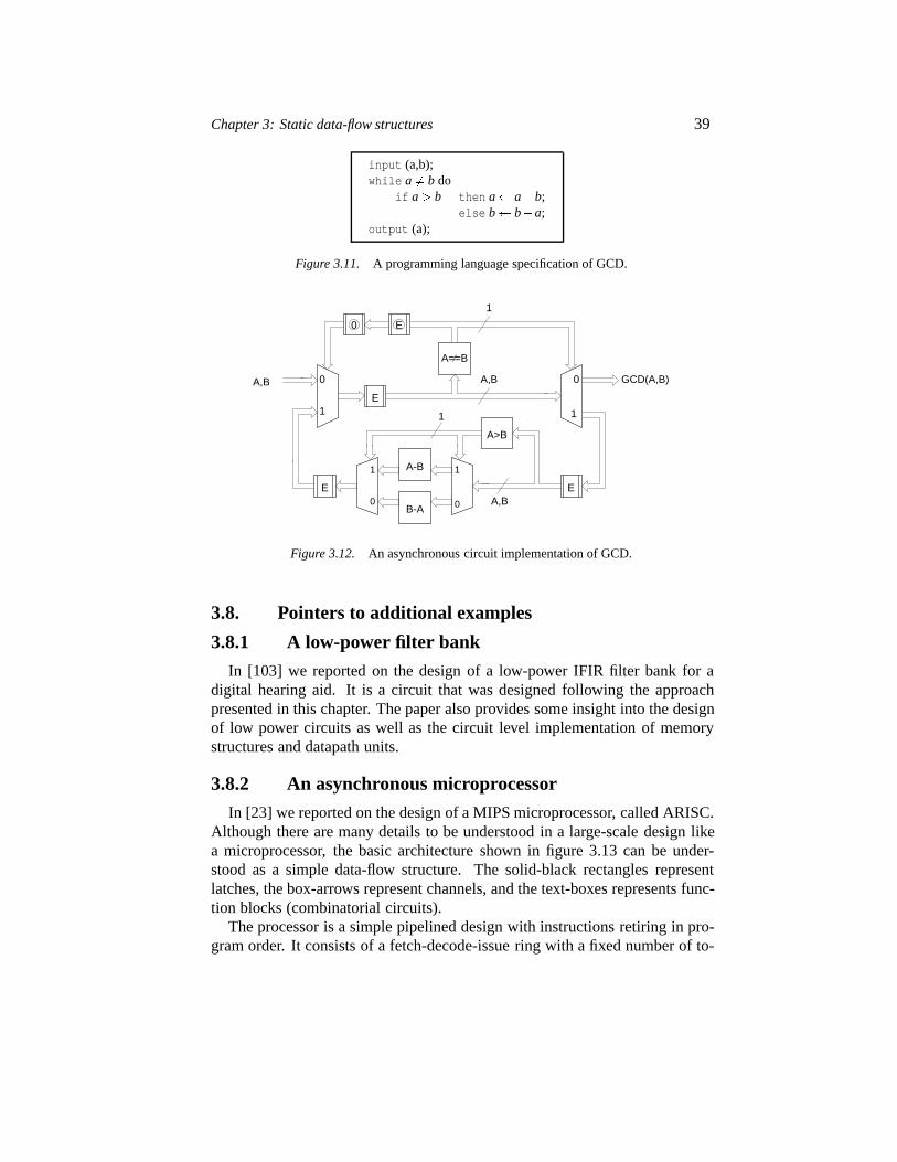
Chapter 3: Static data-flow structures 39
input (a,b);while a �� b do
if a � b then a� a�b;else b� b�a;
output (a);
Figure 3.11. A programming language specification of GCD.
0
1
0
A>B
1
0
1
0
A-B
B-A
0
1
E
E
E E
A==B
A,B GCD(A,B)
A,B
A,B
1
1
Figure 3.12. An asynchronous circuit implementation of GCD.
3.8. Pointers to additional examples
3.8.1 A low-power filter bank
In [103] we reported on the design of a low-power IFIR filter bank for adigital hearing aid. It is a circuit that was designed following the approachpresented in this chapter. The paper also provides some insight into the designof low power circuits as well as the circuit level implementation of memorystructures and datapath units.
3.8.2 An asynchronous microprocessor
In [23] we reported on the design of a MIPS microprocessor, called ARISC.Although there are many details to be understood in a large-scale design likea microprocessor, the basic architecture shown in figure 3.13 can be under-stood as a simple data-flow structure. The solid-black rectangles representlatches, the box-arrows represent channels, and the text-boxes represents func-tion blocks (combinatorial circuits).
The processor is a simple pipelined design with instructions retiring in pro-gram order. It consists of a fetch-decode-issue ring with a fixed number of to-
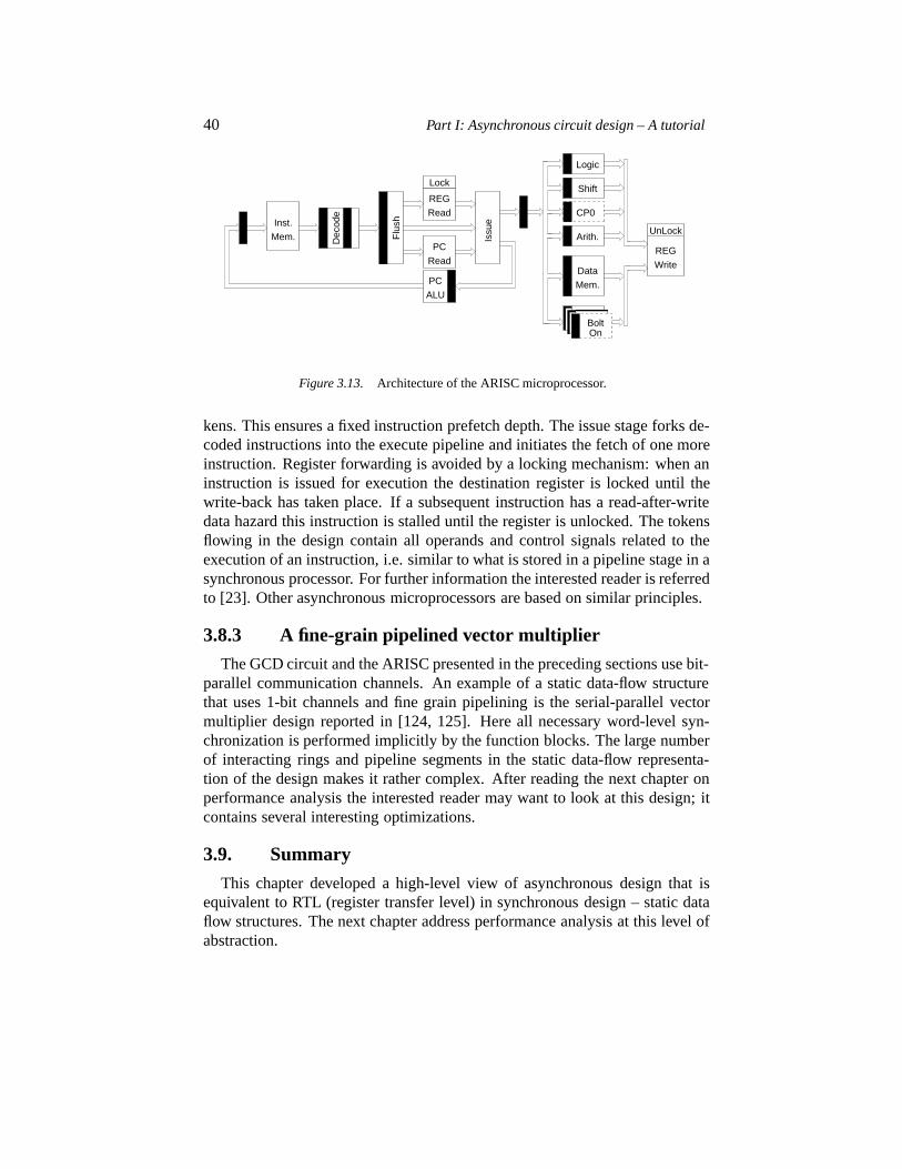
40 Part I: Asynchronous circuit design – A tutorial
REG
Read
PC
Read
PC
ALU
REG
WriteData
Mem.
Inst.
Mem.
OnBolt
Issu
e
Dec
ode
Flu
sh
Arith.
Logic
Shift
CP0
Lock
UnLock
Figure 3.13. Architecture of the ARISC microprocessor.
kens. This ensures a fixed instruction prefetch depth. The issue stage forks de-coded instructions into the execute pipeline and initiates the fetch of one moreinstruction. Register forwarding is avoided by a locking mechanism: when aninstruction is issued for execution the destination register is locked until thewrite-back has taken place. If a subsequent instruction has a read-after-writedata hazard this instruction is stalled until the register is unlocked. The tokensflowing in the design contain all operands and control signals related to theexecution of an instruction, i.e. similar to what is stored in a pipeline stage in asynchronous processor. For further information the interested reader is referredto [23]. Other asynchronous microprocessors are based on similar principles.
3.8.3 A fine-grain pipelined vector multiplier
The GCD circuit and the ARISC presented in the preceding sections use bit-parallel communication channels. An example of a static data-flow structurethat uses 1-bit channels and fine grain pipelining is the serial-parallel vectormultiplier design reported in [124, 125]. Here all necessary word-level syn-chronization is performed implicitly by the function blocks. The large numberof interacting rings and pipeline segments in the static data-flow representa-tion of the design makes it rather complex. After reading the next chapter onperformance analysis the interested reader may want to look at this design; itcontains several interesting optimizations.
3.9. Summary
This chapter developed a high-level view of asynchronous design that isequivalent to RTL (register transfer level) in synchronous design – static dataflow structures. The next chapter address performance analysis at this level ofabstraction.
Chapter 4
PERFORMANCE
In this chapter we will address the performance analysis and optimizationof asynchronous circuits. The material extends and builds upon the “staticdata-flow structures view” introduced in the previous chapter.
4.1. Introduction
In a synchronous circuit, performance analysis and optimization is a matterof finding the longest latency signal path between two registers; this determinesthe period of the clock signal. The global clock partitions the circuit into manycombinatorial circuits that can be analyzed individually. This is known as statictiming analysis and it is a rather simple task, even for a large circuit.
For an asynchronous circuit, performance analysis and optimization is aglobal and therefore much more complex problem. The use of handshakingmakes the timing in one component dependent on the timing of its neighbours,which again depends on the timing of their neighbours, etc. Furthermore, theperformance of a circuit does not depend only on its structure, but also onhow it is initialized and used by its environment. The performance of an asyn-chronous circuit can even exhibit transients and oscillations.
We will first develop a qualitative understanding of the dynamics of the to-ken flow in asynchronous circuits. A good understanding of this is essential fordesigning circuits with good performance. We will then introduce some quan-titative performance parameters that characterize individual pipeline stages andpipelines and rings composed of identical pipeline stages. Using these param-eters one can make first-level design decisions. Finally we will address howmore complex and irregular structures can be analyzed.
The following text represents a major revision of material from [124] andit is based on original work by Ted Williams [153, 154, 155]. If consultingthese references the reader should be aware of the exact definition of a token.Throughout this book a token is defined as a valid data valueor an empty datavalue, whereas in the cited references (that deal exclusively with 4-phase hand-shaking) a token is a valid-empty data pair. The definition used here accentu-ates the similarity between a token in an asynchronous circuit and the token in
41
42 Part I: Asynchronous circuit design – A tutorial
a Petri net. Furthermore it provides some unification between 4-phase hand-shaking and 2-phase handshaking – 2-phase handshaking is the same game,but without empty-tokens.
In the following we will assume 4-phase handshaking, and the examples weprovide all use bundled-data circuits. It is left as an exercise for the readerto make the simple adaptations that are necessary for dealing with 2-phasehandshaking.
4.2. A qualitative view of performance
4.2.1 Example 1: A FIFO used as a shift register
The fundamental concepts can be illustrated by a simple example: a FIFOcomposed of a number of latches in which there areN valid tokens separatedby N empty tokens, and whose environment alternates between reading a tokenfrom the FIFO and writing a token into the FIFO (see figure 4.1(a)). In this waythe nomber of tokens in the FIFO is invariant. This example is relevant becausemany designs use FIFOs in this way, and because it models the behaviour ofshift registers as well as rings – structures in which the number of tokens isalso invariant.
A relevant performance figure is the throughput, which is the rate at whichtokens are input to or output from the shift register. This figure is proportionalto the time it takes to shift the contents of the chain of latches one position tothe right.
Figure 4.1(b) illustrates the behaviour of an implementation in which thereare 2N latches per valid token and figure 4.1(c) illustrates the behaviour of animplementation in which there are 3N latches per valid token. In both exam-ples the number of valid tokens in the FIFO isN � 3, and the only differencebetween the two situations in figure 4.1(b) and 4.1(c) is the number of bubbles.
In figure 4.1(b) at timet1 the environment reads the valid token,D1, asindicated by the solid channel symbol. This introduces a bubble that enablesdata transfers to take place one at a time (t2� t5). At time t6 the environmentinputs a valid token,D4, and at this point all elements have been shifted oneposition to the right. Hence, the time used to move all elements one place tothe right is proportional to the number of tokens, in this case 2N � 6 time steps.
Adding more latches increases the number of bubbles, which again increasesthe number of data transfers that can take place simultaneously, thereby im-proving the performance. In figure 4.1(c) the shift register has 3N stages andtherefore one bubble per valid-empty token-pair. The effect of this is thatNdata transfers can occur simultaneously and the time used to move all elementsone place to the right is constant; 2 time steps.
If the number of latches was increased to 4N there would be one token perbubble, and the time to move all tokens one step to the right would be only
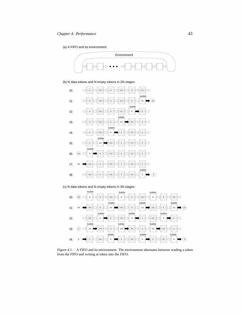
Chapter 4: Performance 43
E D1EE D2
(c) N data tokens and N empty tokens in 3N stages:
(b) N data tokens and N empty tokens in 2N stages:
(a) A FIFO and its environment:
bubble bubble bubble
D3
E EE D2
E E D2
E E
E
D1
E
E
E
D2
D2 E
E
E
D2
D2
E
ED4
D3
D3E
D2ED3D4 E
E D1ED2D3E
EE D1ED2D3D4
ED2ED3ED4
D4
D4 D3 D2
bubblebubblebubble
EEE
bubble bubble bubble
D2D3D4 EEEE
E ED2ED3ED4
E
D4
E
D4
E
Environment
ED2ED3E
E
E Et4:
bubble bubble bubble
D1D3 D2
E E
bubble bubble bubble
t3:
t2:
t1:
t0:
E
bubble
bubble
bubble
bubble
bubble
bubble
bubble
t5:
t4:
t3:
t2:
t1:
t0:
t8:
t7:
t6:
D4
E
D3
E
D2
E E
D1
D3
D3
D3
D3
Figure 4.1. A FIFO and its environment. The environment alternates between reading a tokenfrom the FIFO and writing at token into the FIFO.

44 Part I: Asynchronous circuit design – A tutorial
1 time step. In this situation the pipeline is half full and the latches holdingbubbles act as slave latches (relative to the latches holding tokens). Increasingthe number of bubbles further would not increase the performance further. Fi-nally, it is interesting to notice that the addition of just one more latch holdinga bubble to figure 4.1(b) would double the performance. The asynchronousdesigner has great freedom in trading more latches for performance.
As the number of bubbles in a design depends on the number of latches pertoken, the above analysis illustrates that performance optimization of a givencircuit is primarily a task of structural modification – circuit level optimizationlike transistor sizing is of secondary importance.
4.2.2 Example 2: A shift register with parallel load
In order to illustrate another point – that the distribution of tokens and bub-bles in a circuit can vary over time, depending on the dynamics of the circuitand its environment – we offer another example: a shift register with parallelload. Figure 4.2 shows an initial design of a 4-bit shift register. The circuit hasa bit-parallel input channel,din[3:0], connecting it to a data producing envi-ronment. It also has a 1-bit data channel,do, and a 1-bit control channel,ctl,connecting it to a data consuming environment. Operation is controlled by thedata consuming environment which may request the circuit to: (ctl � 0) per-form a parallel loadand to provide the least significant bit from the bit-parallelchannel on thedo channel, or (ctl � 1) to perform a right shift and providethe next bit on thedo channel. In this way the data consuming environmentalways inputs a control token (valid or empty) to which the circuit always re-sponds by outputting a data token (valid or empty). During a parallel load, theprevious content of the shift register is steered into the “dead end” sink-latches.During a right shift the constant 0 is shifted into the most significant position– corresponding to a logical right shift. The data consuming environment isnot required to read all the input data bits, and it may continue reading zerosbeyond the most significant input data bit.
The initial design shown in figure 4.2 suffers from two performance lim-iting inexpediencies: firstly, it has the same problem as the shift register infigure 4.1(b) – there are too few bubbles, and the peak data rate on the bit-serial output reduces linearly with the length of the shift register. Secondly,the control signal is forked to all of the MUXes and DEMUXes in the design.This implies a high fan-out of the request and data signals (which requires acouple of buffers) and synchronization of all the individual acknowledge sig-nals (which requires a C-element with many inputs, possibly implemented asa tree of C-elements). The first problem can be avoided by adding a 3rd latchto the datapath in each stage of the circuit corresponding to the situation in
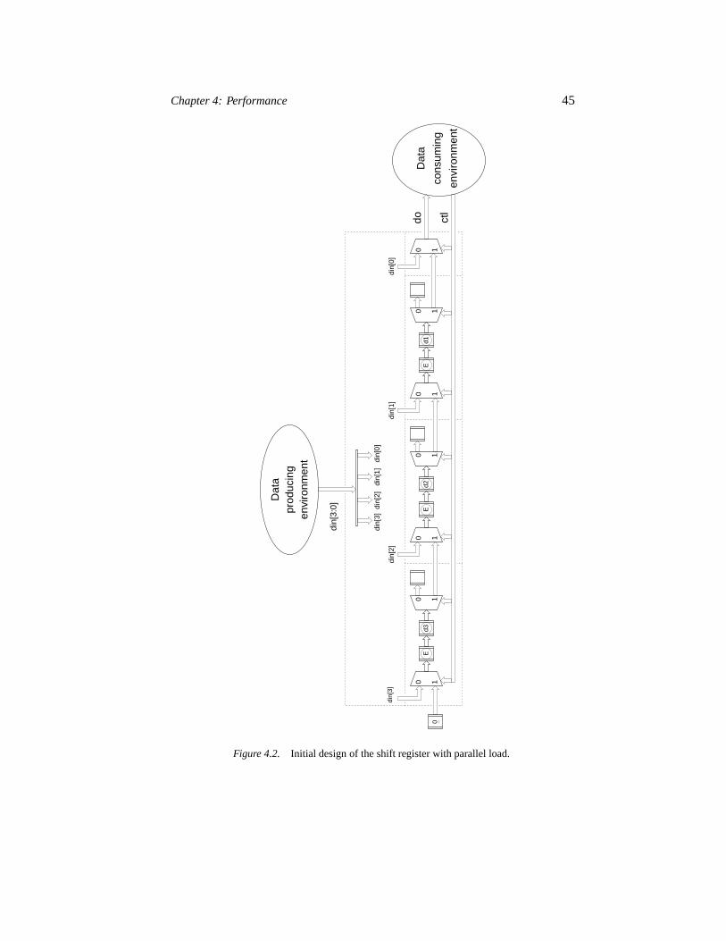
Chapter 4: Performance 45
0 1
0 1
0 1
0 1
0 1
0 110
din[
1]di
n[2]
din[
0]
din[
1]di
n[0]
din[
3]di
n[2]
din[
3:0]prod
ucin
gen
viro
nmen
t
Dat
a
envi
ronm
ent
cons
umin
g
Dat
a
ctl
doE
d3E
d2
din[
3]
Ed1
0
Figure 4.2. Initial design of the shift register with parallel load.
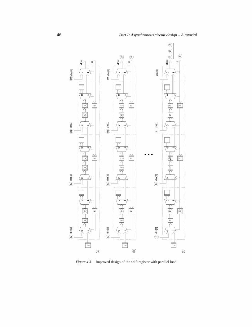
46 Part I: Asynchronous circuit design – A tutorial
0 0 0
100 1
0 1
0 1
0 1
0 1
0 1
ctl
100 1
0 1
0 1
0 1
0 1
0 1
ctl
100 1
0 1
0 1
0 1
0 1
0 1
ctl
din[
0]di
n[2]
din[
3]
din[
3]di
n[2]
din[
1]di
n[0]
dout
dout
dout
din[
0]di
n[1]
din[
2]di
n[3]
E0
E0
E0
d2d1
d3d0
din[
1]
EE
E
E
d3d2
0E
0 EE
E0E
d1d0
d0 0 d1E
d0
E1E
E
E
d2 E
d2
E
E
d3
0
E
(c)
(b)
(a)
Figure 4.3. Improved design of the shift register with parallel load.
Chapter 4: Performance 47
figure 4.1(c), but if the extra latches are added to the control path instead, asshown in figure 4.3(a) on page 46, they will solve both problems.
This improved design exhibits an interesting and illustrative dynamic be-haviour: initially, the data latches are densely packed with tokens and all thecontrol latches contain bubbles, figure 4.3(a). The first step of the parallel loadcycle is shown in figure 4.3(b), and figure 4.3(c) shows a possible state afterthe data consuming environment has read a couple of bits. The most-significantstage is just about to perform its “parallel load” and the bubbles are now in thechain of data latches. If at this point the data consuming environment paused,the tokens in the control path would gradually disappear while tokens in thedatapath would pack again. Note that at any time the total number of tokens inthe circuit is constant!
4.3. Quantifying performance
4.3.1 Latency, throughput and wavelength
When the overall structure of a design is being decided, it is important todetermine the optimal number of latches or pipeline stages in the rings andpipeline fragments from which the design is composed. In order to establish abasis for first order design decisions, this section will introduce some quantita-tive performance parameters. We will restrict the discussion to 4-phase hand-shaking and bundled-data circuit implementations and we will consider ringswith only a single valid token. Subsection 4.3.4, which concludes this sectionon performance parameters, will comment on adapting to other protocols andimplementation styles.
The performance of a pipeline is usually characterized by two parameters:latency andthroughput (or its inverse calledperiod or cycle time). For an asyn-chronous pipeline a third parameter, thedynamic wavelength, is important aswell. With reference to figure 4.4 and following [153, 154, 155] these param-eters are defined as follows:
Latency: The latency is the delay from the input of a data item until the corre-sponding output data item is produced. When data flows in the forwarddirection, acknowledge signals propagate in the reverse direction. Con-sequently two parameters are defined:
The forward latency,Lf , is the delay from new data on the input ofa stage (Data�i�1� or Req�i�1�) to the production of the corre-sponding output (Data�i� or Req�i�) provided that the acknowledgesignals are in place when data arrives.Lf �V and Lf �E denote thelatencies for propagating a valid token and an empty token respec-tively. It is assumed that these latencies are constants, i.e. thatthey are independent of the value of the data. [As forward propa-
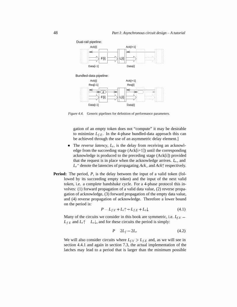
48 Part I: Asynchronous circuit design – A tutorial
Data[i-1]
Req[i-1]
Ack[i] Ack[i+1]
Data[i]
Ack[i]
Data[i-1]
Ack[i+1]
Data[i]
d
Dual-rail pipeline:
Req[i]
Bundled-data pipeline:
L[i]F[i]
L[i]F[i]
Figure 4.4. Generic pipelines for definition of performance parameters.
gation of an empty token does not “compute” it may be desirableto minimizeLf �E . In the 4-phase bundled-data approach this canbe achieved through the use of an asymmetric delay element.]
The reverse latency, Lr, is the delay from receiving an acknowl-edge from the succeeding stage (Ack[i+1]) until the correspondingacknowledge is produced to the preceding stage (Ack[i]) providedthat the request is in place when the acknowledge arrives.Lr andLr denote the latencies of propagatingAck andAck respectively.
Period: The period,P, is the delay between the input of a valid token (fol-lowed by its succeeding empty token) and the input of the next validtoken, i.e. a complete handshake cycle. For a 4-phase protocol this in-volves: (1) forward propagation of a valid data value, (2) reverse propa-gation of acknowledge, (3) forward propagation of the empty data value,and (4) reverse propagation of acknowledge. Therefore a lower boundon the period is:
P � L f �V �Lr�L f �E �Lr (4.1)
Many of the circuits we consider in this book are symmetric, i.e.Lf �V �L f �E andLr� Lr , and for these circuits the period is simply:
P � 2L f �2Lr (4.2)
We will also consider circuits whereLf �V � L f �E and, as we will see insection 4.4.1 and again in section 7.3, the actual implementation of thelatches may lead to a period that is larger than the minimum possible
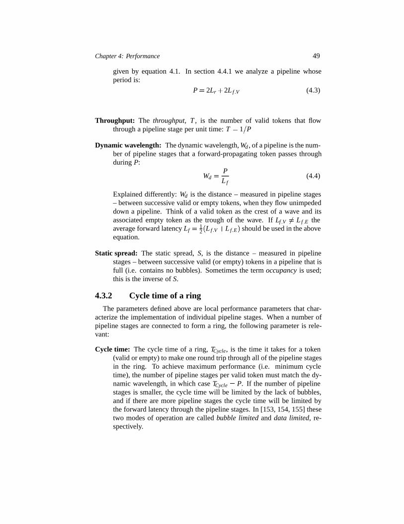
Chapter 4: Performance 49
given by equation 4.1. In section 4.4.1 we analyze a pipeline whoseperiod is:
P � 2Lr �2L f �V (4.3)
Throughput: The throughput, T , is the number of valid tokens that flowthrough a pipeline stage per unit time:T � 1�P
Dynamic wavelength: The dynamic wavelength,Wd , of a pipeline is the num-ber of pipeline stages that a forward-propagating token passes throughduringP:
Wd �PL f
(4.4)
Explained differently:Wd is the distance – measured in pipeline stages– between successive valid or empty tokens, when they flow unimpededdown a pipeline. Think of a valid token as the crest of a wave and itsassociated empty token as the trough of the wave. IfLf �V � L f �E theaverage forward latencyLf �
12�L f �V �L f �E� should be used in the above
equation.
Static spread: The static spread,S, is the distance – measured in pipelinestages – between successive valid (or empty) tokens in a pipeline that isfull (i.e. contains no bubbles). Sometimes the termoccupancy is used;this is the inverse ofS.
4.3.2 Cycle time of a ring
The parameters defined above are local performance parameters that char-acterize the implementation of individual pipeline stages. When a number ofpipeline stages are connected to form a ring, the following parameter is rele-vant:
Cycle time: The cycle time of a ring,TCycle, is the time it takes for a token(valid or empty) to make one round trip through all of the pipeline stagesin the ring. To achieve maximum performance (i.e. minimum cycletime), the number of pipeline stages per valid token must match the dy-namic wavelength, in which caseTCycle � P. If the number of pipelinestages is smaller, the cycle time will be limited by the lack of bubbles,and if there are more pipeline stages the cycle time will be limited bythe forward latency through the pipeline stages. In [153, 154, 155] thesetwo modes of operation are calledbubble limited anddata limited, re-spectively.
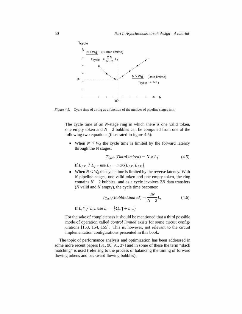
50 Part I: Asynchronous circuit design – A tutorial
Wd
cycleT
N < W :d
Tcycle =2 N
LN - 2 r
(Bubble limited)
N > W :d
Tcycle = N Lf
(Data limited)
N
P
Figure 4.5. Cycle time of a ring as a function of the number of pipeline stages in it.
The cycle time of anN-stage ring in which there is one valid token,one empty token andN�2 bubbles can be computed from one of thefollowing two equations (illustrated in figure 4.5):
When N �Wd the cycle time is limited by the forward latencythrough the N stages:
TCycle�DataLimited� � N�Lf (4.5)
If L f �V � L f �E useLf � max�L f �V ;L f �E�.
WhenN �Wd the cycle time is limited by the reverse latency. WithN pipeline stages, one valid token and one empty token, the ringcontainsN�2 bubbles, and as a cycle involves 2N data transfers(N valid andN empty), the cycle time becomes:
TCycle�BubbleLimited� �2N
N�2Lr (4.6)
If Lr � Lr useLr �12�Lr�Lr �
For the sake of completeness it should be mentioned that a third possiblemode of operation calledcontrol limited exists for some circuit config-urations [153, 154, 155]. This is, however, not relevant to the circuitimplementation configurations presented in this book.
The topic of performance analysis and optimization has been addressed insome more recent papers [31, 90, 91, 37] and in some of these the term “slackmatching” is used (referring to the process of balancing the timing of forwardflowing tokens and backward flowing bubbles).
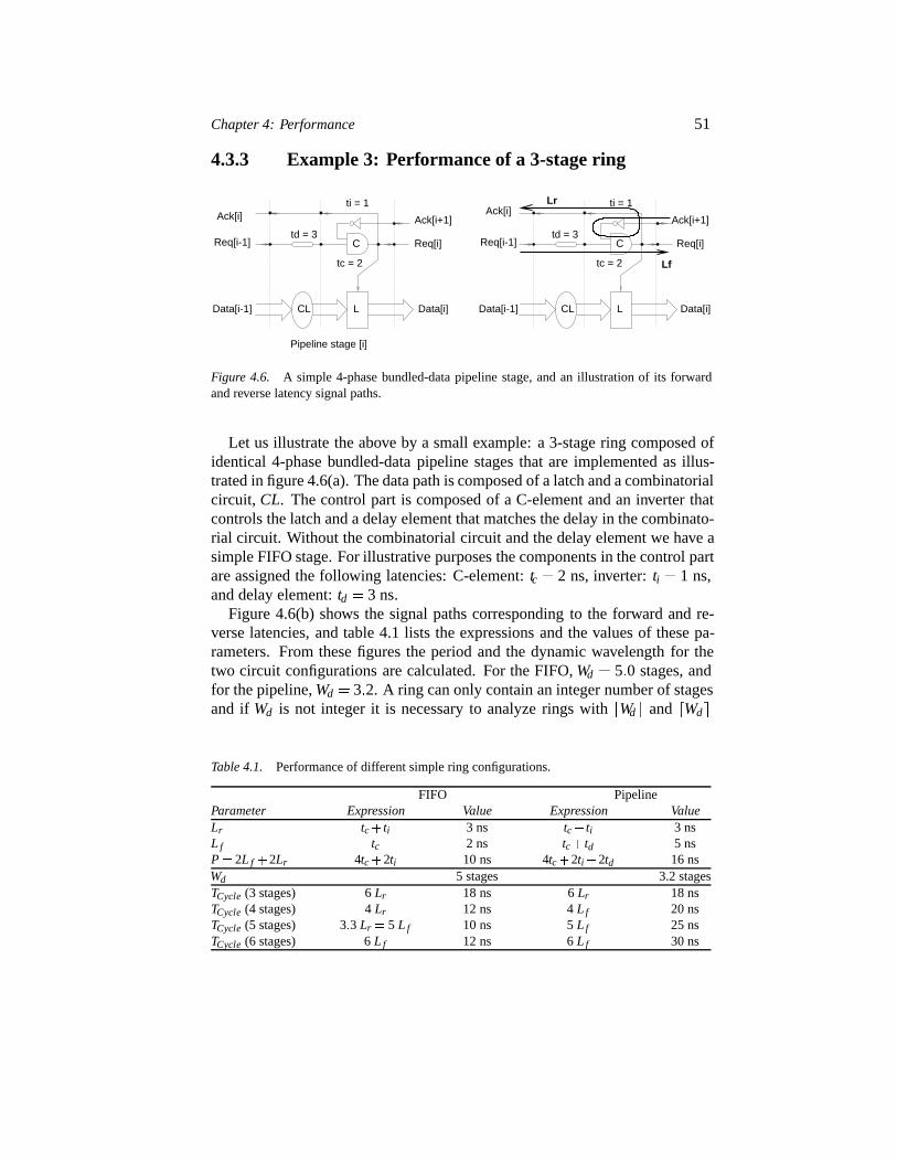
Chapter 4: Performance 51
4.3.3 Example 3: Performance of a 3-stage ring
Pipeline stage [i]
Req[i-1]
Data[i-1] Data[i]
Req[i]
Ack[i+1]Ack[i]
CL L
ti = 1
Lf
LrAck[i]
Req[i-1] Req[i]
Ack[i+1]
Data[i]Data[i-1] CL L
ti = 1
td = 3 td = 3
tc = 2tc = 2
C C
Figure 4.6. A simple 4-phase bundled-data pipeline stage, and an illustration of its forwardand reverse latency signal paths.
Let us illustrate the above by a small example: a 3-stage ring composed ofidentical 4-phase bundled-data pipeline stages that are implemented as illus-trated in figure 4.6(a). The data path is composed of a latch and a combinatorialcircuit, CL. The control part is composed of a C-element and an inverter thatcontrols the latch and a delay element that matches the delay in the combinato-rial circuit. Without the combinatorial circuit and the delay element we have asimple FIFO stage. For illustrative purposes the components in the control partare assigned the following latencies: C-element:tc � 2 ns, inverter:ti � 1 ns,and delay element:td � 3 ns.
Figure 4.6(b) shows the signal paths corresponding to the forward and re-verse latencies, and table 4.1 lists the expressions and the values of these pa-rameters. From these figures the period and the dynamic wavelength for thetwo circuit configurations are calculated. For the FIFO,Wd � 5�0 stages, andfor the pipeline,Wd � 3�2. A ring can only contain an integer number of stagesand if Wd is not integer it is necessary to analyze rings with�Wd� and�Wd�
Table 4.1. Performance of different simple ring configurations.
FIFO PipelineParameter Expression Value Expression ValueLr tc� ti 3 ns tc� ti 3 nsL f tc 2 ns tc� td 5 nsP� 2L f �2Lr 4tc�2ti 10 ns 4tc�2ti�2td 16 nsWd 5 stages 3.2 stagesTCycle (3 stages) 6Lr 18 ns 6Lr 18 nsTCycle (4 stages) 4Lr 12 ns 4Lf 20 nsTCycle (5 stages) 3�3 Lr � 5 L f 10 ns 5Lf 25 nsTCycle (6 stages) 6L f 12 ns 6Lf 30 ns
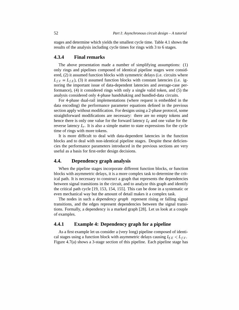
52 Part I: Asynchronous circuit design – A tutorial
stages and determine which yields the smallest cycle time. Table 4.1 shows theresults of the analysis including cycle times for rings with 3 to 6 stages.
4.3.4 Final remarks
The above presentation made a number of simplifying assumptions: (1)only rings and pipelines composed of identical pipeline stages were consid-ered, (2) it assumed function blocks with symmetric delays (i.e. circuits whereL f �V � L f �E), (3) it assumed function blocks with constant latencies (i.e. ig-noring the important issue of data-dependent latencies and average-case per-formance), (4) it considered rings with only a single valid token, and (5) theanalysis considered only 4-phase handshaking and bundled-data circuits.
For 4-phase dual-rail implementations (where request is embedded in thedata encoding) the performance parameter equations defined in the previoussection apply without modification. For designs using a 2-phase protocol, somestraightforward modifications are necessary: there are no empty tokens andhence there is only one value for the forward latencyLf and one value for thereverse latencyLr. It is also a simple matter to state expressions for the cycletime of rings with more tokens.
It is more difficult to deal with data-dependent latencies in the functionblocks and to deal with non-identical pipeline stages. Despite these deficien-cies the performance parameters introduced in the previous sections are veryuseful as a basis for first-order design decisions.
4.4. Dependency graph analysis
When the pipeline stages incorporate different function blocks, or functionblocks with asymmetric delays, it is a more complex task to determine the crit-ical path. It is necessary to construct a graph that represents the dependenciesbetween signal transitions in the circuit, and to analyze this graph and identifythe critical path cycle [19, 153, 154, 155]. This can be done in a systematic oreven mechanical way but the amount of detail makes it a complex task.
The nodes in such adependency graph represent rising or falling signaltransitions, and the edges represent dependencies between the signal transi-tions. Formally, a dependency is a marked graph [28]. Let us look at a coupleof examples.
4.4.1 Example 4: Dependency graph for a pipeline
As a first example let us consider a (very long) pipeline composed of identi-cal stages using a function block with asymmetric delays causingLf �E � L f �V .Figure 4.7(a) shows a 3-stage section of this pipeline. Each pipeline stage has
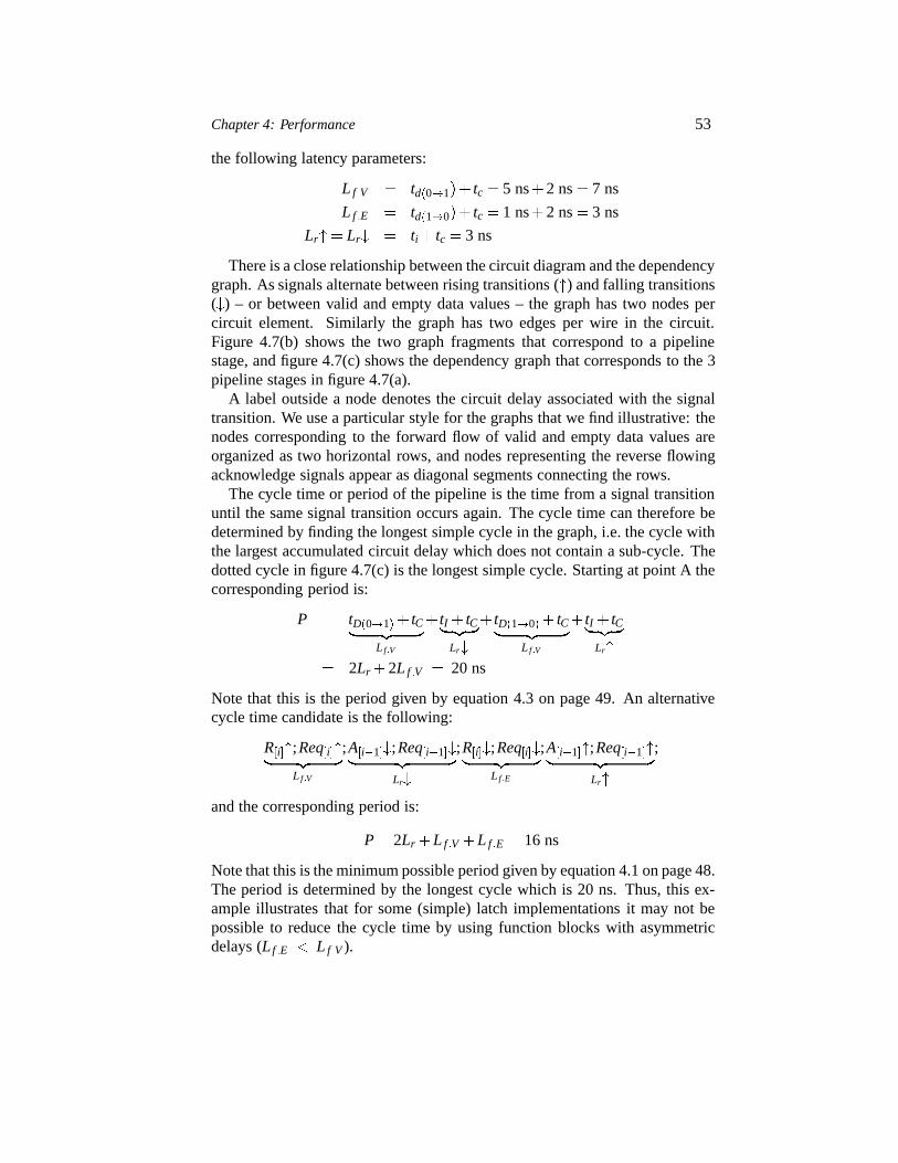
Chapter 4: Performance 53
the following latency parameters:
L f �V � td�0�1�� tc � 5 ns�2 ns� 7 ns
L f �E � td�1�0�� tc � 1 ns�2 ns� 3 ns
Lr� Lr � ti � tc � 3 ns
There is a close relationship between the circuit diagram and the dependencygraph. As signals alternate between rising transitions () and falling transitions( ) – or between valid and empty data values – the graph has two nodes percircuit element. Similarly the graph has two edges per wire in the circuit.Figure 4.7(b) shows the two graph fragments that correspond to a pipelinestage, and figure 4.7(c) shows the dependency graph that corresponds to the 3pipeline stages in figure 4.7(a).
A label outside a node denotes the circuit delay associated with the signaltransition. We use a particular style for the graphs that we find illustrative: thenodes corresponding to the forward flow of valid and empty data values areorganized as two horizontal rows, and nodes representing the reverse flowingacknowledge signals appear as diagonal segments connecting the rows.
The cycle time or period of the pipeline is the time from a signal transitionuntil the same signal transition occurs again. The cycle time can therefore bedetermined by finding the longest simple cycle in the graph, i.e. the cycle withthe largest accumulated circuit delay which does not contain a sub-cycle. Thedotted cycle in figure 4.7(c) is the longest simple cycle. Starting at point A thecorresponding period is:
P � tD�0�1�� tC� �� �
Lf �V
� tI � tC� �� �
Lr
� tD�1�0�� tC� �� �
Lf �V
� tI � tC� �� �
Lr
� 2Lr �2L f �V � 20 ns
Note that this is the period given by equation 4.3 on page 49. An alternativecycle time candidate is the following:
R�i�;Req�i�� �� �
Lf �V
;A�i�1� ;Req�i�1� � �� �
Lr
;R�i� ;Req�i� � �� �
Lf �E
;A�i�1�;Req�i�1�� �� �
Lr
;
and the corresponding period is:
P � 2Lr �L f �V �L f �E � 16 ns
Note that this is the minimum possible period given by equation 4.1 on page 48.The period is determined by the longest cycle which is 20 ns. Thus, this ex-ample illustrates that for some (simple) latch implementations it may not bepossible to reduce the cycle time by using function blocks with asymmetricdelays (Lf �E � L f �V ).
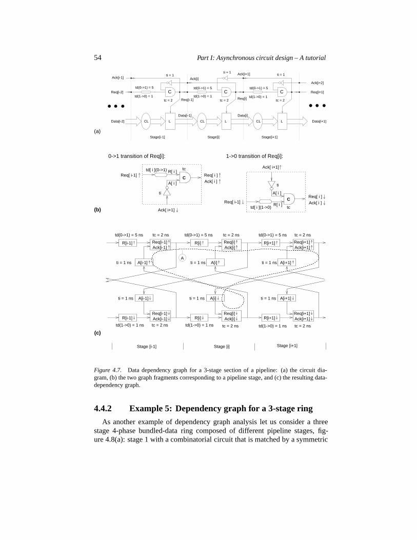
54 Part I: Asynchronous circuit design – A tutorial
L
CLL
CLL
CL
ti = 1
Ack[i-1] Ack[i]
Stage[i-1] Stage[i] Stage[i+1]
Data[i-1]
td(0->1) = 5 td(0->1) = 5
Req[i-1]
td(0->1) = 5
Req[i]
ti = 1
Req[i-2]
Data[i-2]
Ack[i+2]
Req[i+1]
Data[i+1]
Ack[i+1]
Data[i]
ti = 1
td(1->0) = 1 td(1->0) = 1 td(1->0) = 1tc = 2 tc = 2 tc = 2
(a)
CCC
Req[ i ]
Ack[ i ]Req[ i-1]tc
ti
Ack[ i+1]
R[ i ]
A[ i ]
td[ i ](1->0)
tc
ti
R[ i ]
A[ i ]
Ack[ i+1]
td[ i ](0->1)Req[ i ]
Ack[ i ]
0->1 transition of Req[i]: 1->0 transition of Req[i]:
ti = 1 ns ti = 1 ns
ti = 1 ns ti = 1 ns
tc = 2 ns
tc = 2 ns
tc = 2 ns
tc = 2 ns
tc = 2 ns
ti = 1 ns
tc = 2 ns
R[i-1] R[i]
td(0->1) = 5 nstd(0->1) = 5 ns td(0->1) = 5 ns
Ack[i]R[i+1]
Ack[i+1]Req[i] Req[i+1]Req[i-1]
A[i-1] A[i] A[i+1]
A[i-1] A[i] A[i+1]
R[i-1] Ack[i-1]Req[i-1]
td(1->0) = 1 ns td(1->0) = 1 ns
R[i] Ack[i]Req[i]
td(1->0) = 1 ns
R[i+1]Req[i+1]Ack[i+1]
ti = 1 ns
Stage [i]Stage [i-1] Stage [i+1]
Ack[i-1]
A
C
CReq[ i-1]
(b)
(c)
Figure 4.7. Data dependency graph for a 3-stage section of a pipeline: (a) the circuit dia-gram, (b) the two graph fragments corresponding to a pipeline stage, and (c) the resulting data-dependency graph.
4.4.2 Example 5: Dependency graph for a 3-stage ring
As another example of dependency graph analysis let us consider a threestage 4-phase bundled-data ring composed of different pipeline stages, fig-ure 4.8(a): stage 1 with a combinatorial circuit that is matched by a symmetric
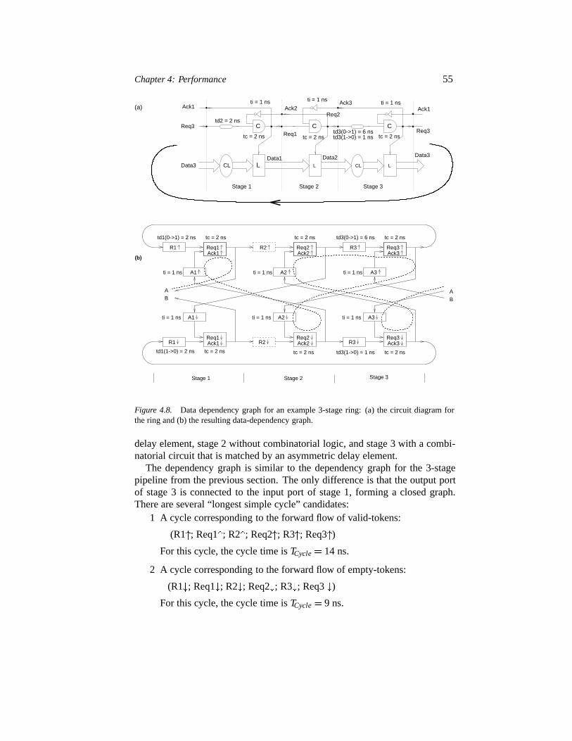
Chapter 4: Performance 55
L
CLL
(a)
L
Ack1
Req3
Data3 CLData1
Ack2
Req1
Ack3
Data2
Stage 2Stage 1
Ack1
Req3
Data3
Stage 3
tc = 2 ns
ti = 1 ns ti = 1 ns
Req2
td3(0->1) = 6 nstd3(1->0) = 1 ns tc = 2 ns
ti = 1 ns
td2 = 2 ns
tc = 2 ns
CCC
B
A
B
A
R1
A1
Req1Ack1
ti = 1 ns
ti = 1 ns ti = 1 ns
R1
A1
Req1Ack1 R2
A2
Req2Ack2
ti = 1 ns ti = 1 ns
R3 Req3Ack3
A3
td1(0->1) = 2 ns tc = 2 ns
R2
A2
Req2Ack2
tc = 2 ns
tc = 2 ns
tc = 2 nstd1(1->0) = 2 ns
td3(0->1) = 6 ns tc = 2 ns
Req3Ack3
A3
R3
ti = 1 ns
tc = 2 ns
Stage 1 Stage 2 Stage 3
td3(1->0) = 1 ns
(b)
Figure 4.8. Data dependency graph for an example 3-stage ring: (a) the circuit diagram forthe ring and (b) the resulting data-dependency graph.
delay element, stage 2 without combinatorial logic, and stage 3 with a combi-natorial circuit that is matched by an asymmetric delay element.
The dependency graph is similar to the dependency graph for the 3-stagepipeline from the previous section. The only difference is that the output portof stage 3 is connected to the input port of stage 1, forming a closed graph.There are several “longest simple cycle” candidates:
1 A cycle corresponding to the forward flow of valid-tokens:
(R1; Req1; R2; Req2; R3; Req3)
For this cycle, the cycle time isTCycle � 14 ns.
2 A cycle corresponding to the forward flow of empty-tokens:
(R1 ; Req1 ; R2 ; Req2 ; R3 ; Req3 )
For this cycle, the cycle time isTCycle � 9 ns.
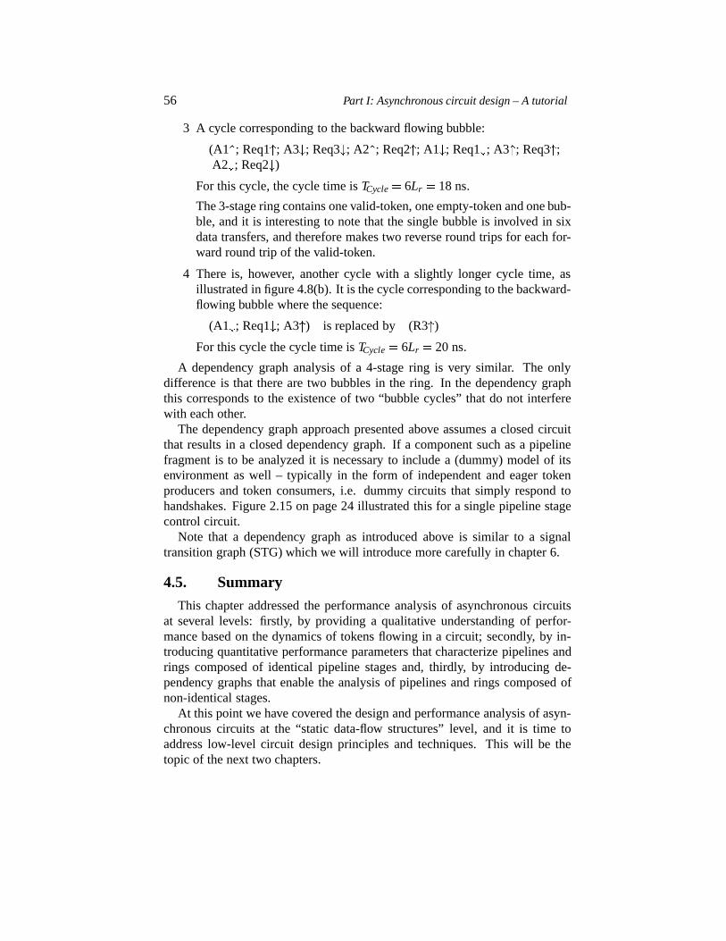
56 Part I: Asynchronous circuit design – A tutorial
3 A cycle corresponding to the backward flowing bubble:
(A1; Req1; A3 ; Req3 ; A2; Req2; A1 ; Req1 ; A3; Req3;A2 ; Req2 )
For this cycle, the cycle time isTCycle � 6Lr � 18 ns.
The 3-stage ring contains one valid-token, one empty-token and one bub-ble, and it is interesting to note that the single bubble is involved in sixdata transfers, and therefore makes two reverse round trips for each for-ward round trip of the valid-token.
4 There is, however, another cycle with a slightly longer cycle time, asillustrated in figure 4.8(b). It is the cycle corresponding to the backward-flowing bubble where the sequence:
(A1 ; Req1 ; A3) is replaced by (R3)
For this cycle the cycle time isTCycle � 6Lr � 20 ns.
A dependency graph analysis of a 4-stage ring is very similar. The onlydifference is that there are two bubbles in the ring. In the dependency graphthis corresponds to the existence of two “bubble cycles” that do not interferewith each other.
The dependency graph approach presented above assumes a closed circuitthat results in a closed dependency graph. If a component such as a pipelinefragment is to be analyzed it is necessary to include a (dummy) model of itsenvironment as well – typically in the form of independent and eager tokenproducers and token consumers, i.e. dummy circuits that simply respond tohandshakes. Figure 2.15 on page 24 illustrated this for a single pipeline stagecontrol circuit.
Note that a dependency graph as introduced above is similar to a signaltransition graph (STG) which we will introduce more carefully in chapter 6.
4.5. Summary
This chapter addressed the performance analysis of asynchronous circuitsat several levels: firstly, by providing a qualitative understanding of perfor-mance based on the dynamics of tokens flowing in a circuit; secondly, by in-troducing quantitative performance parameters that characterize pipelines andrings composed of identical pipeline stages and, thirdly, by introducing de-pendency graphs that enable the analysis of pipelines and rings composed ofnon-identical stages.
At this point we have covered the design and performance analysis of asyn-chronous circuits at the “static data-flow structures” level, and it is time toaddress low-level circuit design principles and techniques. This will be thetopic of the next two chapters.
Chapter 5
HANDSHAKE CIRCUIT IMPLEMENTATIONS
In this chapter we will address the implementation of handshake compo-nents. First, we will consider the basic set of components introduced in sec-tion 3.3 on page 32: (1) the latch, (2) the unconditional data-flow control el-ements join, fork and merge, (3) function blocks, and (4) the conditional flowcontrol elements MUX and DEMUX. In addition to these basic componentswe will also consider the implementation of mutual exclusion elements andarbiters and touch upon the (unavoidable) problem of metastability. The majorpart of the chapter (sections 5.3–5.6) is devoted to the implementation of func-tion blocks and the material includes a number of fundamental concepts andcircuit implementation styles.
5.1. The latch
As mentioned previously, the role of latches is: (1) to provide storage forvalid and empty tokens, and (2) to support the flow of tokens via handshak-ing with neighbouring latches. Possible implementations of the handshakelatch were shown in chapter 2: Figure 2.9 on page 18 shows how a 4-phasebundled-data handshake latch can be implemented using a conventional latchand a control circuit (the figure shows several such examples assembled intopipelines). In a similar way figure 2.11 on page 20 shows the implementationof a 2-phase bundled-data latch, and figures 2.12-2.13 on page 21 show theimplementation of a 4-phase dual-rail latch.
A handshake latch can be characterized in terms of thethroughput, thedy-namic wavelength and thestatic spread of a FIFO that is composed of identicallatches. Common to the two 4-phase latch designs mentioned above is that aFIFO will fill with every other latch holding a valid token and every other latchholding an empty token (as illustrated in figure 4.1(b) on page 43). Thus, thestatic spread for these FIFOs isS � 2.
A 2-phase implementation does not involve empty tokens and consequentlyit may be possible to design a latch whose static spread isS � 1. Note, how-ever, that the implementation of the 2-phase bundled-data handshake latch in
57
58 Part I: Asynchronous circuit design – A tutorial
figure 2.11 on page 20 involves several level-sensitive latches; the utilizationof the level sensitive latches is no better.
Ideally, one would want to pack a valid token into every level-sensitive latch,and in chapter 7 we will address the design of 4-phase bundled-data handshakelatches that have a smaller static spread.
5.2. Fork, join, and merge
Possible 4-phase bundled-data and 4-phase dual-rail implementations of thefork, join, and merge components are shown in figure 5.1. For simplicity thefigure shows a fork with two output channels only, and join and merge compo-nents with two input channels only. Furthermore, all channels are assumed tobe 1-bit channels. It is, of course, possible to generalize to three or more inputsand outputs respectively, and to extend ton-bit channels. Based on the expla-nation given below this should be straightforward, and it is left as an exercisefor the reader.
4-phase fork and join A fork involves a C-element to combine the acknowl-edge signals on the output channels into a single acknowledge signal on theinput channel. Similarly a 4-phase bundled-data join involves a C-element tocombine the request signals on the input channels into a single request signalon the output channel. The 4-phase dual-rail join does not involve any activecomponents as the request signal is encoded into the data.
The particular fork in figure 5.1 duplicates the input data, and the join con-catenates the input data. This happens to be the way joins and forks are mostlyused in our static data-flow structures, but there are many alternatives: for ex-ample, the fork could split the input data which would make it more symmetricto the join in figure 5.1. In any case the difference is only in how the input datais transferred to the output. From a control point of view the different alter-natives are identical: a join synchronizes several input channels and a forksynchronizes several output channels.
4-phase merge The implementation of the merge is a little more elaborate.Handshakes on the input channels are mutually exclusive, and the merge sim-ply relays the active input handshake to the output channel.
Let us consider the implementation of the 4-phase bundled-data merge first.It consists of an asynchronous control circuit and a multiplexer that is con-trolled by the input request. The control circuit is explained below.
The request signals on the input channels are mutually exclusive and maysimply be ORed together to produce the request signal on the output channel.
For each input channel, a C-element produces an acknowledge signal in re-sponse to an acknowledge on the output channel provided that the input chan-nel has valid data. For example, the C-element driving thexack signal is set high
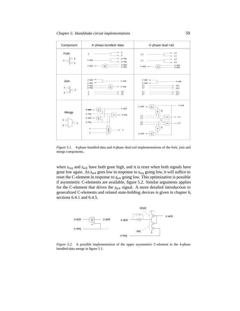
Chapter 5: Handshake circuit implementations 59
C
1)
y
1)
y
x.fz.f
y
Merge
Join
C
C
y−req
y−ackz−ack
x−req
y
z
z−req
x−ack
x
y.f
MU
X
x−ack
x−req
z.t
y.t
x−ack
x
x.t
x−ack
y
z−acky−ack
z0.f
z−ack
z−req
Fork
y−ack
xy z1
z0
z0.ty−ack
x−ack
x.tx.f
z1.tz1.f
z
y−ack
y−req
z−req
Component 4−phase bundled−data 4−phase dual−rail
x−ack z−ack
x−reqy−req
z.f
x−ack
y−ack
z−ack
z−ack
z.t x.t x.f
y.t y.f
y.ty.f
C
CC
+
++
+
Cz
+
x
x
z
z
x
Figure 5.1. 4-phase bundled-data and 4-phase dual-rail implementations of the fork, join andmerge components.
whenxreq andzack have both gone high, and it is reset when both signals havegone low again. Aszack goes low in response toxreq going low, it will suffice toreset the C-element in response tozack going low. This optimization is possibleif asymmetric C-elements are available, figure 5.2. Similar arguments appliesfor the C-element that drives theyack signal. A more detailed introduction togeneralized C-elements and related state-holding devices is given in chapter 6,sections 6.4.1 and 6.4.5.
+
Cx-ack z-ack
x-req
z-ackx-ack
reset
x-req
set
Figure 5.2. A possible implementation of the upper asymmetric C-element in the 4-phasebundled-data merge in figure 5.1.
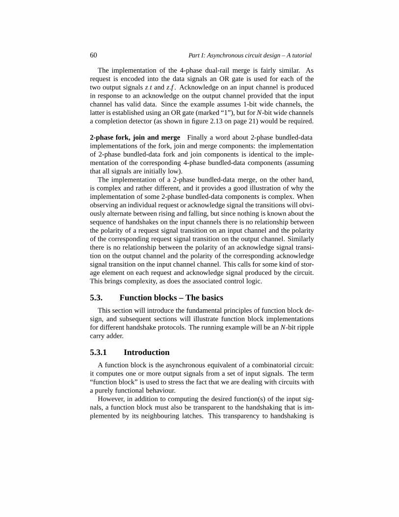
60 Part I: Asynchronous circuit design – A tutorial
The implementation of the 4-phase dual-rail merge is fairly similar. Asrequest is encoded into the data signals an OR gate is used for each of thetwo output signalsz�t andz�f . Acknowledge on an input channel is producedin response to an acknowledge on the output channel provided that the inputchannel has valid data. Since the example assumes 1-bit wide channels, thelatter is established using an OR gate (marked “1”), but forN-bit wide channelsa completion detector (as shown in figure 2.13 on page 21) would be required.
2-phase fork, join and merge Finally a word about 2-phase bundled-dataimplementations of the fork, join and merge components: the implementationof 2-phase bundled-data fork and join components is identical to the imple-mentation of the corresponding 4-phase bundled-data components (assumingthat all signals are initially low).
The implementation of a 2-phase bundled-data merge, on the other hand,is complex and rather different, and it provides a good illustration of why theimplementation of some 2-phase bundled-data components is complex. Whenobserving an individual request or acknowledge signal the transitions will obvi-ously alternate between rising and falling, but since nothing is known about thesequence of handshakes on the input channels there is no relationship betweenthe polarity of a request signal transition on an input channel and the polarityof the corresponding request signal transition on the output channel. Similarlythere is no relationship between the polarity of an acknowledge signal transi-tion on the output channel and the polarity of the corresponding acknowledgesignal transition on the input channel channel. This calls for some kind of stor-age element on each request and acknowledge signal produced by the circuit.This brings complexity, as does the associated control logic.
5.3. Function blocks – The basics
This section will introduce the fundamental principles of function block de-sign, and subsequent sections will illustrate function block implementationsfor different handshake protocols. The running example will be anN-bit ripplecarry adder.
5.3.1 Introduction
A function block is the asynchronous equivalent of a combinatorial circuit:it computes one or more output signals from a set of input signals. The term“function block” is used to stress the fact that we are dealing with circuits witha purely functional behaviour.
However, in addition to computing the desired function(s) of the input sig-nals, a function block must also be transparent to the handshaking that is im-plemented by its neighbouring latches. This transparency to handshaking is
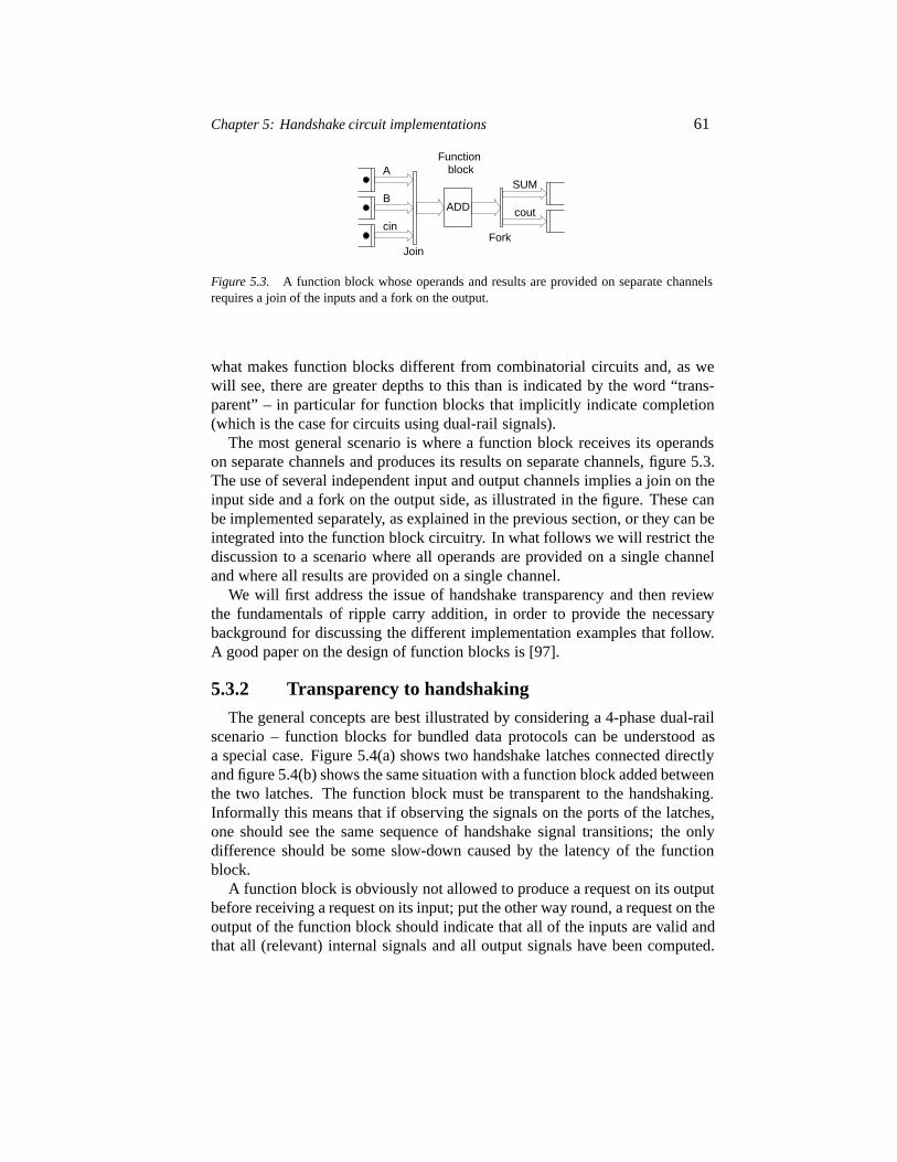
Chapter 5: Handshake circuit implementations 61
blockFunction
A
BSUM
ADD
cincout
JoinFork
Figure 5.3. A function block whose operands and results are provided on separate channelsrequires a join of the inputs and a fork on the output.
what makes function blocks different from combinatorial circuits and, as wewill see, there are greater depths to this than is indicated by the word “trans-parent” – in particular for function blocks that implicitly indicate completion(which is the case for circuits using dual-rail signals).
The most general scenario is where a function block receives its operandson separate channels and produces its results on separate channels, figure 5.3.The use of several independent input and output channels implies a join on theinput side and a fork on the output side, as illustrated in the figure. These canbe implemented separately, as explained in the previous section, or they can beintegrated into the function block circuitry. In what follows we will restrict thediscussion to a scenario where all operands are provided on a single channeland where all results are provided on a single channel.
We will first address the issue of handshake transparency and then reviewthe fundamentals of ripple carry addition, in order to provide the necessarybackground for discussing the different implementation examples that follow.A good paper on the design of function blocks is [97].
5.3.2 Transparency to handshaking
The general concepts are best illustrated by considering a 4-phase dual-railscenario – function blocks for bundled data protocols can be understood asa special case. Figure 5.4(a) shows two handshake latches connected directlyand figure 5.4(b) shows the same situation with a function block added betweenthe two latches. The function block must be transparent to the handshaking.Informally this means that if observing the signals on the ports of the latches,one should see the same sequence of handshake signal transitions; the onlydifference should be some slow-down caused by the latency of the functionblock.
A function block is obviously not allowed to produce a request on its outputbefore receiving a request on its input; put the other way round, a request on theoutput of the function block should indicate that all of the inputs are valid andthat all (relevant) internal signals and all output signals have been computed.
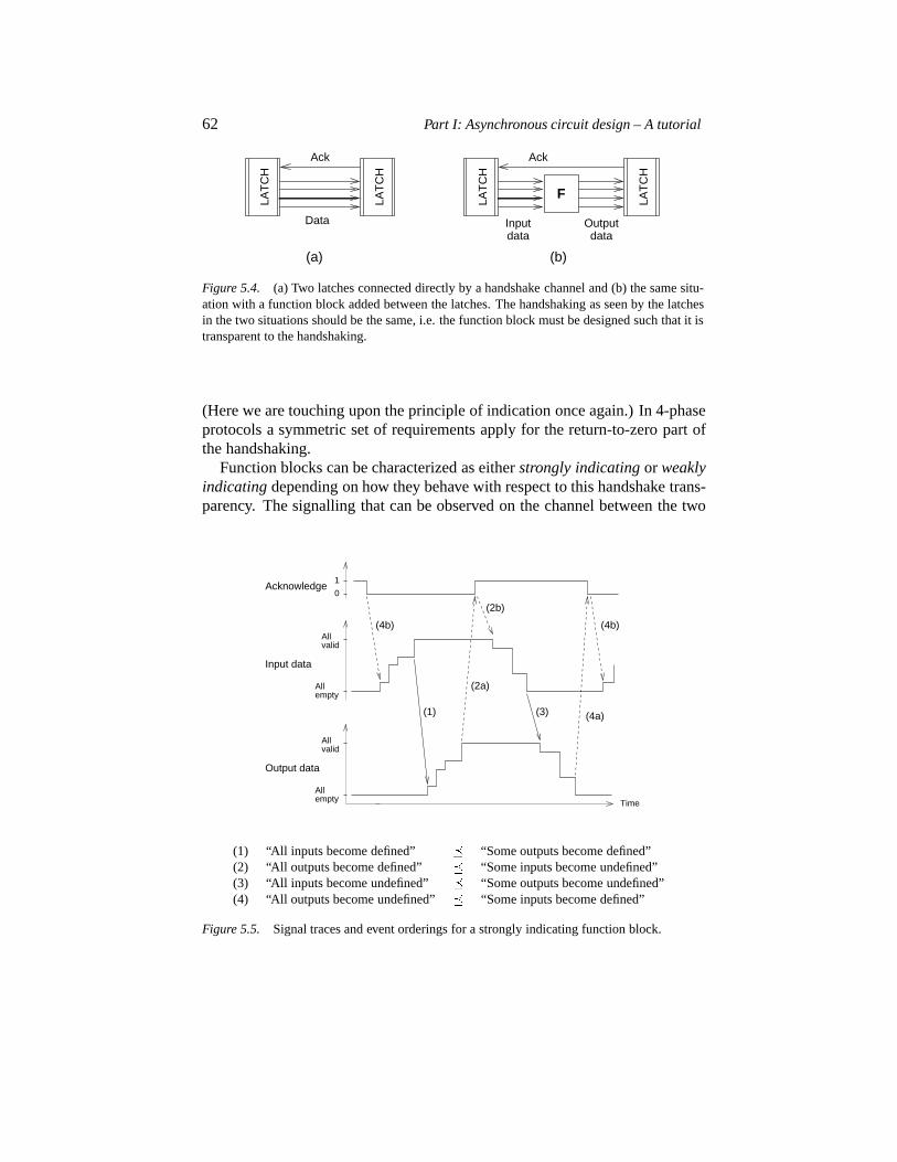
62 Part I: Asynchronous circuit design – A tutorial
Ack
Data
Ack
F
Inputdata
Outputdata
(b)(a)LA
TC
H
LAT
CH
LAT
CH
LAT
CH
Figure 5.4. (a) Two latches connected directly by a handshake channel and (b) the same situ-ation with a function block added between the latches. The handshaking as seen by the latchesin the two situations should be the same, i.e. the function block must be designed such that it istransparent to the handshaking.
(Here we are touching upon the principle of indication once again.) In 4-phaseprotocols a symmetric set of requirements apply for the return-to-zero part ofthe handshaking.
Function blocks can be characterized as eitherstrongly indicating or weaklyindicating depending on how they behave with respect to this handshake trans-parency. The signalling that can be observed on the channel between the two
Allvalid
Allempty
Allvalid
Allempty
Acknowledge1
0
Time
Input data
Output data
(1)
(2a)
(2b)
(3) (4a)
(4b)(4b)
(1) “All inputs become defined” � “Some outputs become defined”(2) “All outputs become defined” � “Some inputs become undefined”(3) “All inputs become undefined” � “Some outputs become undefined”(4) “All outputs become undefined” � “Some inputs become defined”
Figure 5.5. Signal traces and event orderings for a strongly indicating function block.
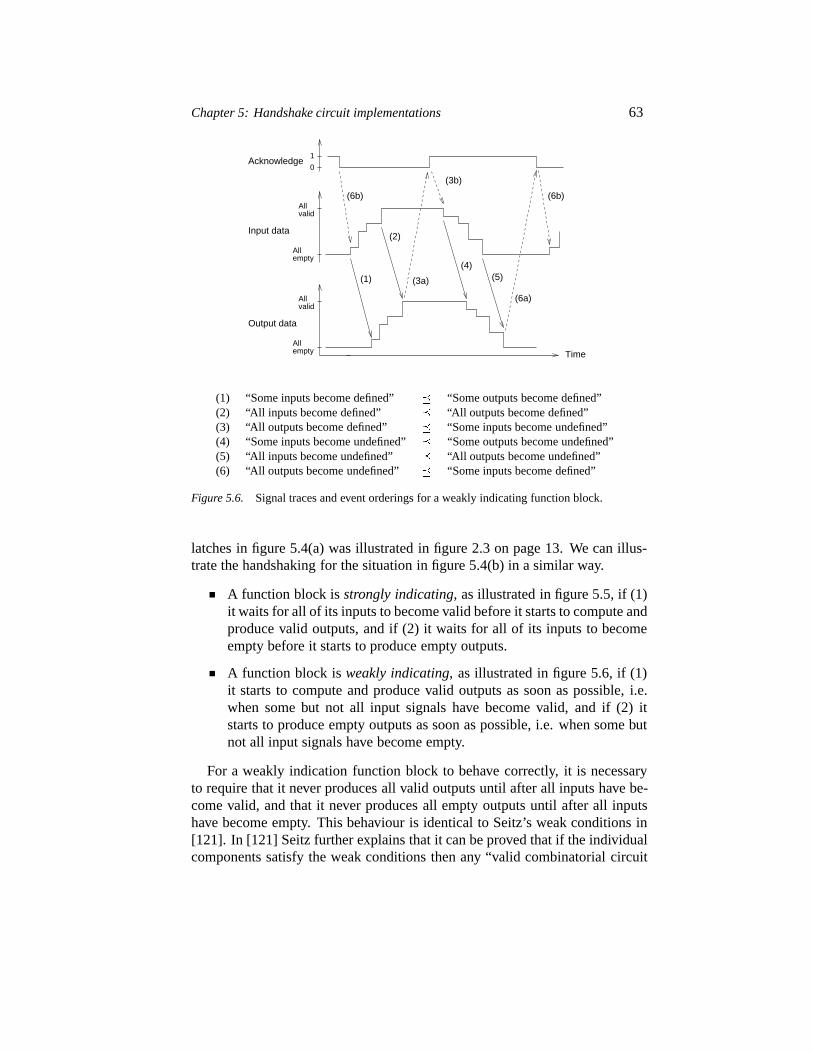
Chapter 5: Handshake circuit implementations 63
Allvalid
Allempty
Allvalid
Allempty
Acknowledge1
0
Time
Input data
Output data
(6b)
(3b)
(6a)
(6b)
(2)
(1) (3a)
(4)(5)
(1) “Some inputs become defined” � “Some outputs become defined”(2) “All inputs become defined” � “All outputs become defined”(3) “All outputs become defined” � “Some inputs become undefined”(4) “Some inputs become undefined”� “Some outputs become undefined”(5) “All inputs become undefined” � “All outputs become undefined”(6) “All outputs become undefined” � “Some inputs become defined”
Figure 5.6. Signal traces and event orderings for a weakly indicating function block.
latches in figure 5.4(a) was illustrated in figure 2.3 on page 13. We can illus-trate the handshaking for the situation in figure 5.4(b) in a similar way.
A function block isstrongly indicating, as illustrated in figure 5.5, if (1)it waits for all of its inputs to become valid before it starts to compute andproduce valid outputs, and if (2) it waits for all of its inputs to becomeempty before it starts to produce empty outputs.
A function block isweakly indicating, as illustrated in figure 5.6, if (1)it starts to compute and produce valid outputs as soon as possible, i.e.when some but not all input signals have become valid, and if (2) itstarts to produce empty outputs as soon as possible, i.e. when some butnot all input signals have become empty.
For a weakly indication function block to behave correctly, it is necessaryto require that it never produces all valid outputs until after all inputs have be-come valid, and that it never produces all empty outputs until after all inputshave become empty. This behaviour is identical to Seitz’s weak conditions in[121]. In [121] Seitz further explains that it can be proved that if the individualcomponents satisfy the weak conditions then any “valid combinatorial circuit
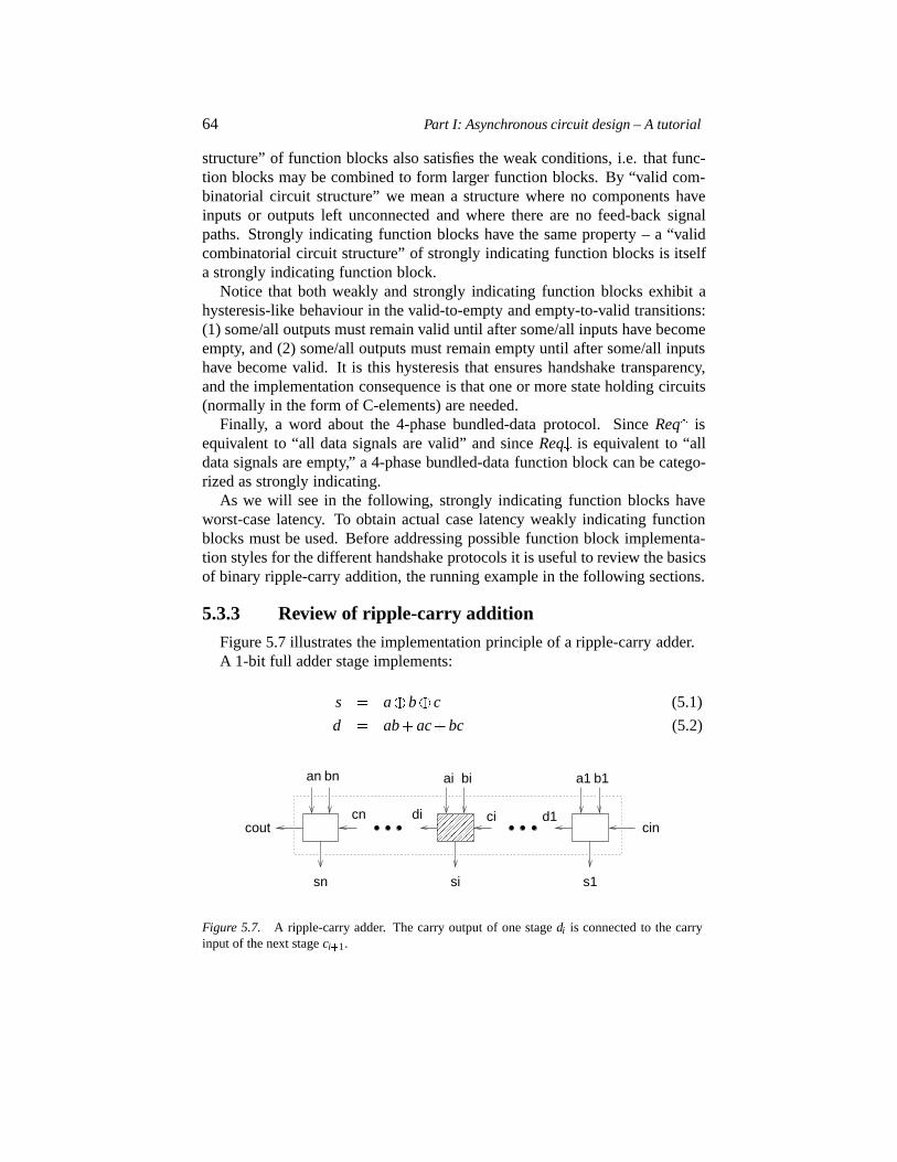
64 Part I: Asynchronous circuit design – A tutorial
structure” of function blocks also satisfies the weak conditions, i.e. that func-tion blocks may be combined to form larger function blocks. By “valid com-binatorial circuit structure” we mean a structure where no components haveinputs or outputs left unconnected and where there are no feed-back signalpaths. Strongly indicating function blocks have the same property – a “validcombinatorial circuit structure” of strongly indicating function blocks is itselfa strongly indicating function block.
Notice that both weakly and strongly indicating function blocks exhibit ahysteresis-like behaviour in the valid-to-empty and empty-to-valid transitions:(1) some/all outputs must remain valid until after some/all inputs have becomeempty, and (2) some/all outputs must remain empty until after some/all inputshave become valid. It is this hysteresis that ensures handshake transparency,and the implementation consequence is that one or more state holding circuits(normally in the form of C-elements) are needed.
Finally, a word about the 4-phase bundled-data protocol. SinceReq isequivalent to “all data signals are valid” and sinceReq is equivalent to “alldata signals are empty,” a 4-phase bundled-data function block can be catego-rized as strongly indicating.
As we will see in the following, strongly indicating function blocks haveworst-case latency. To obtain actual case latency weakly indicating functionblocks must be used. Before addressing possible function block implementa-tion styles for the different handshake protocols it is useful to review the basicsof binary ripple-carry addition, the running example in the following sections.
5.3.3 Review of ripple-carry addition
Figure 5.7 illustrates the implementation principle of a ripple-carry adder.A 1-bit full adder stage implements:
s � a�b� c (5.1)
d � ab�ac�bc (5.2)
ai bi a1 b1an bn
��������������������
��������������������di d1cicn
sn si s1
cout cin
Figure 5.7. A ripple-carry adder. The carry output of one stagedi is connected to the carryinput of the next stageci�1.
Chapter 5: Handshake circuit implementations 65
In many implementations inputsa andb are recoded as:
p � a�b (“propagate” carry) (5.3)
g � ab (“generate” carry) (5.4)
k � ab (“kill” carry) (5.5)
� � �and the output signals are computed as follows:
s � p� c (5.6)
d � g� pc or alternatively (5.7a)
d � k� pc (5.7b)
For a ripple-carry adder, the worst case critical path is a carry rippling acrossthe entire adder. If the latency of a 1-bit full adder istadd the worst case latencyof an N-bit adder isN � tadd. This is a very rare situation and in general thelongest carry ripple during a computation is much shorter. Assuming randomand uncorrelated operands the average latency islog�N� � tadd and, if numeri-cally small operands occur more frequently, the average latency is even less.Using normal Boolean signals (as in the bundled-data protocols) there is noway to know when the computation has finished and the resulting performanceis thus worst-case.
By using dual-rail carry signals (d�t�d�f ) it is possible to design circuitsthat indicate completion as part of the computation and thus achieve actualcase latency. The crux is that a dual-rail carry signal,d, conveys one of thefollowing 3 messages:
(d�t�d�f ) = (0,0) = Empty “The carry has not been computed yet”(possibly because it depends onc)
(d�t�d�f ) = (1,0) = True “The carry is 1”(d�t�d�f ) = (0,1) = False “The carry is 0”
Consequently it is possible for a 1-bit adder to output a valid carry withoutwaiting for the incoming carry if its inputs make this possible (a � b � 0 ora � b � 1). This idea was first put forward in 1955 in a paper by Gilchrist [52].The same idea is explained in [62, pp. 75-78] and in [121].
5.4. Bundled-data function blocks
5.4.1 Using matched delays
A bundled-data implementation of the adder in figure 5.7 is shown in fig-ure 5.8. It is composed of a traditional combinatorial circuit adder and a match-ing delay element. The delay element provides a constant delay that matchestheworst case latency of the combinatorial adder. This includes the worst case
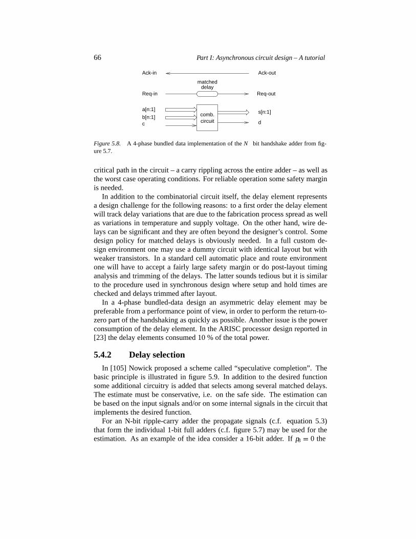
66 Part I: Asynchronous circuit design – A tutorial
comb.circuit
s[n:1]
d
a[n:1]
b[n:1]c
matcheddelay
Req-in Req-out
Ack-in Ack-out
Figure 5.8. A 4-phase bundled data implementation of theN�bit handshake adder from fig-ure 5.7.
critical path in the circuit – a carry rippling across the entire adder – as well asthe worst case operating conditions. For reliable operation some safety marginis needed.
In addition to the combinatorial circuit itself, the delay element representsa design challenge for the following reasons: to a first order the delay elementwill track delay variations that are due to the fabrication process spread as wellas variations in temperature and supply voltage. On the other hand, wire de-lays can be significant and they are often beyond the designer’s control. Somedesign policy for matched delays is obviously needed. In a full custom de-sign environment one may use a dummy circuit with identical layout but withweaker transistors. In a standard cell automatic place and route environmentone will have to accept a fairly large safety margin or do post-layout timinganalysis and trimming of the delays. The latter sounds tedious but it is similarto the procedure used in synchronous design where setup and hold times arechecked and delays trimmed after layout.
In a 4-phase bundled-data design an asymmetric delay element may bepreferable from a performance point of view, in order to perform the return-to-zero part of the handshaking as quickly as possible. Another issue is the powerconsumption of the delay element. In the ARISC processor design reported in[23] the delay elements consumed 10 % of the total power.
5.4.2 Delay selection
In [105] Nowick proposed a scheme called “speculative completion”. Thebasic principle is illustrated in figure 5.9. In addition to the desired functionsome additional circuitry is added that selects among several matched delays.The estimate must be conservative, i.e. on the safe side. The estimation canbe based on the input signals and/or on some internal signals in the circuit thatimplements the desired function.
For an N-bit ripple-carry adder the propagate signals (c.f. equation 5.3)that form the individual 1-bit full adders (c.f. figure 5.7) may be used for theestimation. As an example of the idea consider a 16-bit adder. Ifp8 � 0 the
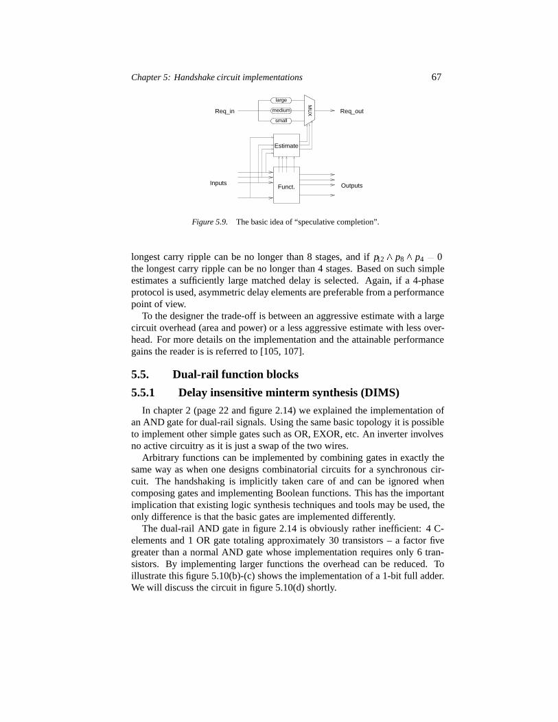
Chapter 5: Handshake circuit implementations 67
large
small
medium
Estimate
Funct.
Req_in Req_out
Inputs Outputs
MU
X
Figure 5.9. The basic idea of “speculative completion”.
longest carry ripple can be no longer than 8 stages, and ifp12� p8� p4 � 0the longest carry ripple can be no longer than 4 stages. Based on such simpleestimates a sufficiently large matched delay is selected. Again, if a 4-phaseprotocol is used, asymmetric delay elements are preferable from a performancepoint of view.
To the designer the trade-off is between an aggressive estimate with a largecircuit overhead (area and power) or a less aggressive estimate with less over-head. For more details on the implementation and the attainable performancegains the reader is is referred to [105, 107].
5.5. Dual-rail function blocks
5.5.1 Delay insensitive minterm synthesis (DIMS)
In chapter 2 (page 22 and figure 2.14) we explained the implementation ofan AND gate for dual-rail signals. Using the same basic topology it is possibleto implement other simple gates such as OR, EXOR, etc. An inverter involvesno active circuitry as it is just a swap of the two wires.
Arbitrary functions can be implemented by combining gates in exactly thesame way as when one designs combinatorial circuits for a synchronous cir-cuit. The handshaking is implicitly taken care of and can be ignored whencomposing gates and implementing Boolean functions. This has the importantimplication that existing logic synthesis techniques and tools may be used, theonly difference is that the basic gates are implemented differently.
The dual-rail AND gate in figure 2.14 is obviously rather inefficient: 4 C-elements and 1 OR gate totaling approximately 30 transistors – a factor fivegreater than a normal AND gate whose implementation requires only 6 tran-sistors. By implementing larger functions the overhead can be reduced. Toillustrate this figure 5.10(b)-(c) shows the implementation of a 1-bit full adder.We will discuss the circuit in figure 5.10(d) shortly.
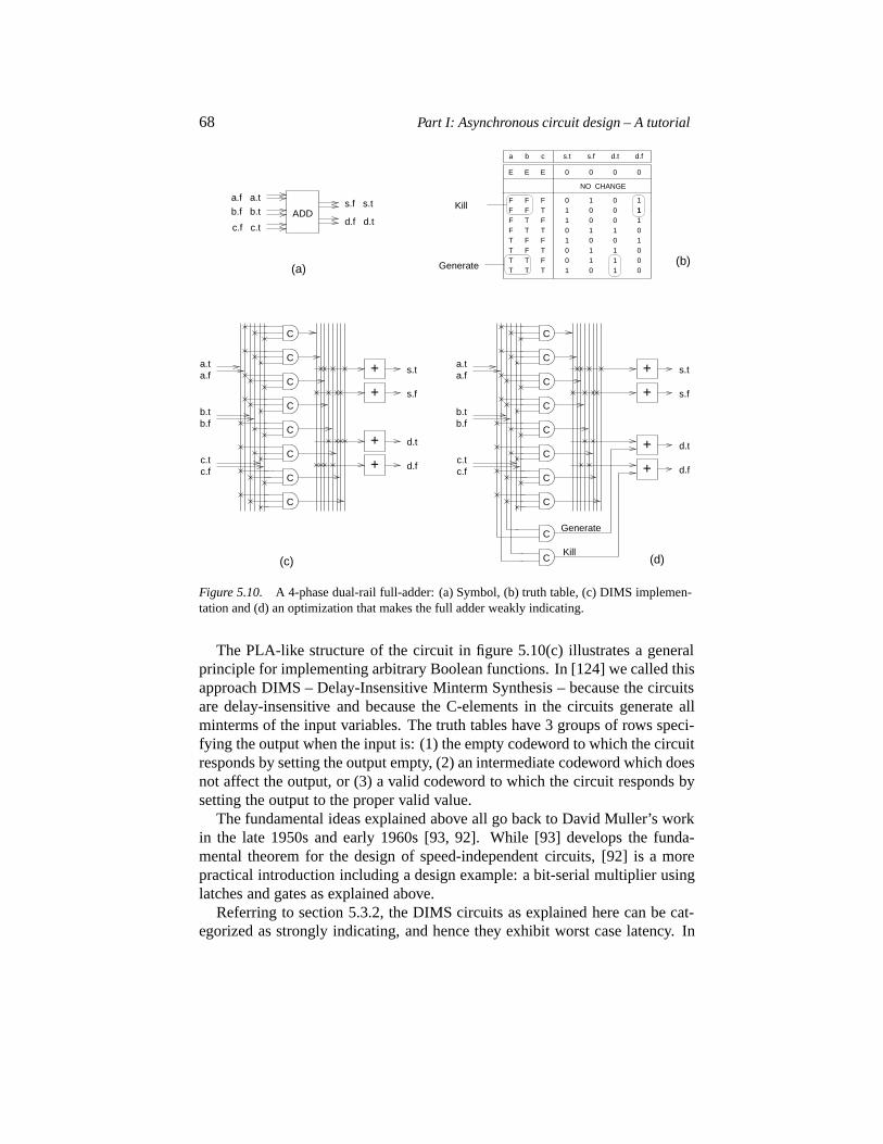
68 Part I: Asynchronous circuit design – A tutorial
b.f b.t
c.f c.t
s.f s.t
d.f d.t
Generate
Kill
E E E 0 0 0 0
cba
F F FTFF
F T FTTF
T F FTFT
T T FTTT
0101101001 0
1101
00
00
0
11
1
1
1
101
00
0
NO CHANGE
Kill
Generate
s.t s.f d.t d.f
(b)
(d)(c)
(a)
C
C
C
C
C
C
C
C
b.f
c.f
b.t
c.t
a.fa.t +
+
+
+
s.t
s.f
d.t
d.f
ADD
a.f a.t
C
C
C
C
C
C
C
C
b.f
c.f
b.t
c.t
a.fa.t
C
C
+
+
+
+
s.t
s.f
d.t
d.f
1
Figure 5.10. A 4-phase dual-rail full-adder: (a) Symbol, (b) truth table, (c) DIMS implemen-tation and (d) an optimization that makes the full adder weakly indicating.
The PLA-like structure of the circuit in figure 5.10(c) illustrates a generalprinciple for implementing arbitrary Boolean functions. In [124] we called thisapproach DIMS – Delay-Insensitive Minterm Synthesis – because the circuitsare delay-insensitive and because the C-elements in the circuits generate allminterms of the input variables. The truth tables have 3 groups of rows speci-fying the output when the input is: (1) the empty codeword to which the circuitresponds by setting the output empty, (2) an intermediate codeword which doesnot affect the output, or (3) a valid codeword to which the circuit responds bysetting the output to the proper valid value.
The fundamental ideas explained above all go back to David Muller’s workin the late 1950s and early 1960s [93, 92]. While [93] develops the funda-mental theorem for the design of speed-independent circuits, [92] is a morepractical introduction including a design example: a bit-serial multiplier usinglatches and gates as explained above.
Referring to section 5.3.2, the DIMS circuits as explained here can be cat-egorized as strongly indicating, and hence they exhibit worst case latency. In
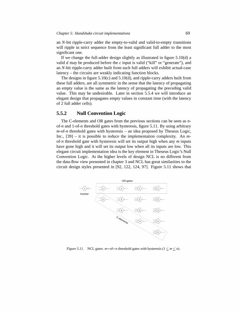
Chapter 5: Handshake circuit implementations 69
an N-bit ripple-carry adder the empty-to-valid and valid-to-empty transitionswill ripple in strict sequence from the least significant full adder to the mostsignificant one.
If we change the full-adder design slightly as illustrated in figure 5.10(d) avalid d may be produced before thec input is valid (“kill” or “generate”), andanN-bit ripple-carry adder built from such full adders will exhibit actual-caselatency – the circuits are weakly indicating function blocks.
The designs in figure 5.10(c) and 5.10(d), and ripple-carry adders built fromthese full adders, are all symmetric in the sense that the latency of propagatingan empty value is the same as the latency of propagating the preceding validvalue. This may be undesirable. Later in section 5.5.4 we will introduce anelegant design that propagates empty values in constant time (with the latencyof 2 full adder cells).
5.5.2 Null Convention Logic
The C-elements and OR gates from the previous sections can be seen asn-of-n and 1-of-n threshold gates with hysteresis, figure 5.11. By using arbitrarym-of-n threshold gates with hysteresis – an idea proposed by Theseus Logic,Inc., [39] – it is possible to reduce the implementation complexity. Anm-of-n threshold gate with hysteresis will set its output high when anym inputshave gone high and it will set its output low when all its inputs are low. Thiselegant circuit implementation idea is the key element in Theseus Logic’s NullConvention Logic. At the higher levels of design NCL is no different fromthe data-flow view presented in chapter 3 and NCL has great similarities to thecircuit design styles presented in [92, 122, 124, 97]. Figure 5.11 shows that
1 1
2 2
3
5
1 1 1
2 2
33
4 4
C-elements
Inverter
OR-gates
Figure 5.11. NCL gates:m�of�n threshold gates with hysteresis (1� m� n).
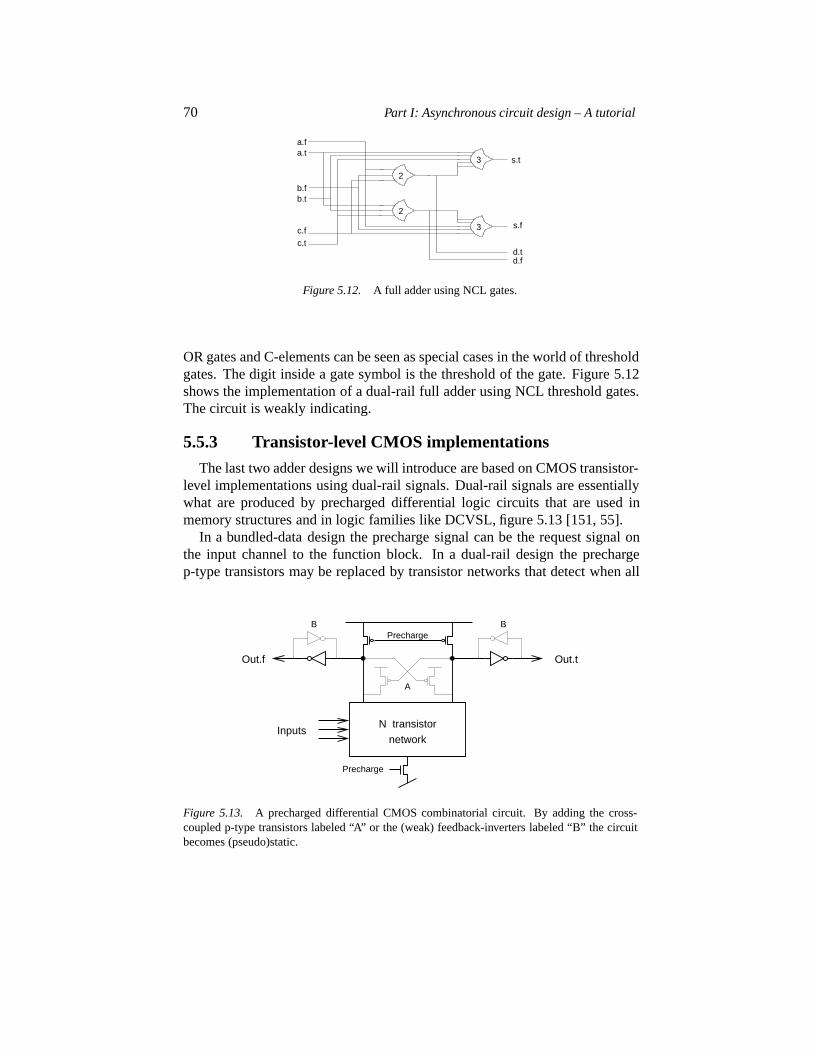
70 Part I: Asynchronous circuit design – A tutorial
2
2
3
3
b.fb.t
c.t
c.f
a.ta.f
s.t
s.f
d.td.f
Figure 5.12. A full adder using NCL gates.
OR gates and C-elements can be seen as special cases in the world of thresholdgates. The digit inside a gate symbol is the threshold of the gate. Figure 5.12shows the implementation of a dual-rail full adder using NCL threshold gates.The circuit is weakly indicating.
5.5.3 Transistor-level CMOS implementations
The last two adder designs we will introduce are based on CMOS transistor-level implementations using dual-rail signals. Dual-rail signals are essentiallywhat are produced by precharged differential logic circuits that are used inmemory structures and in logic families like DCVSL, figure 5.13 [151, 55].
In a bundled-data design the precharge signal can be the request signal onthe input channel to the function block. In a dual-rail design the prechargep-type transistors may be replaced by transistor networks that detect when all
A
B B
Precharge
N transistor
network
Out.t
Inputs
Precharge
Out.f
Figure 5.13. A precharged differential CMOS combinatorial circuit. By adding the cross-coupled p-type transistors labeled “A” or the (weak) feedback-inverters labeled “B” the circuitbecomes (pseudo)static.
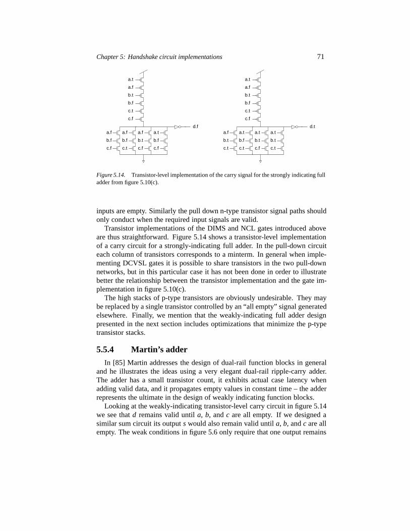
Chapter 5: Handshake circuit implementations 71
c.f
c.t
b.t
a.f
b.f
c.f
c.t
b.t
a.f
b.f
b.t
c.f
b.f
c.t
d.f
b.f
c.f
b.f
c.f
d.t
b.t
c.f
b.t
c.t
b.f
c.t
b.t
c.t
a.t a.t
a.ta.f a.f a.f a.ta.f a.t a.t
Figure 5.14. Transistor-level implementation of the carry signal for the strongly indicating fulladder from figure 5.10(c).
inputs are empty. Similarly the pull down n-type transistor signal paths shouldonly conduct when the required input signals are valid.
Transistor implementations of the DIMS and NCL gates introduced aboveare thus straightforward. Figure 5.14 shows a transistor-level implementationof a carry circuit for a strongly-indicating full adder. In the pull-down circuiteach column of transistors corresponds to a minterm. In general when imple-menting DCVSL gates it is possible to share transistors in the two pull-downnetworks, but in this particular case it has not been done in order to illustratebetter the relationship between the transistor implementation and the gate im-plementation in figure 5.10(c).
The high stacks of p-type transistors are obviously undesirable. They maybe replaced by a single transistor controlled by an “all empty” signal generatedelsewhere. Finally, we mention that the weakly-indicating full adder designpresented in the next section includes optimizations that minimize the p-typetransistor stacks.
5.5.4 Martin’s adder
In [85] Martin addresses the design of dual-rail function blocks in generaland he illustrates the ideas using a very elegant dual-rail ripple-carry adder.The adder has a small transistor count, it exhibits actual case latency whenadding valid data, and it propagates empty values in constant time – the adderrepresents the ultimate in the design of weakly indicating function blocks.
Looking at the weakly-indicating transistor-level carry circuit in figure 5.14we see thatd remains valid untila, b, andc are all empty. If we designed asimilar sum circuit its outputs would also remain valid untila, b, andc are allempty. The weak conditions in figure 5.6 only require that one output remains
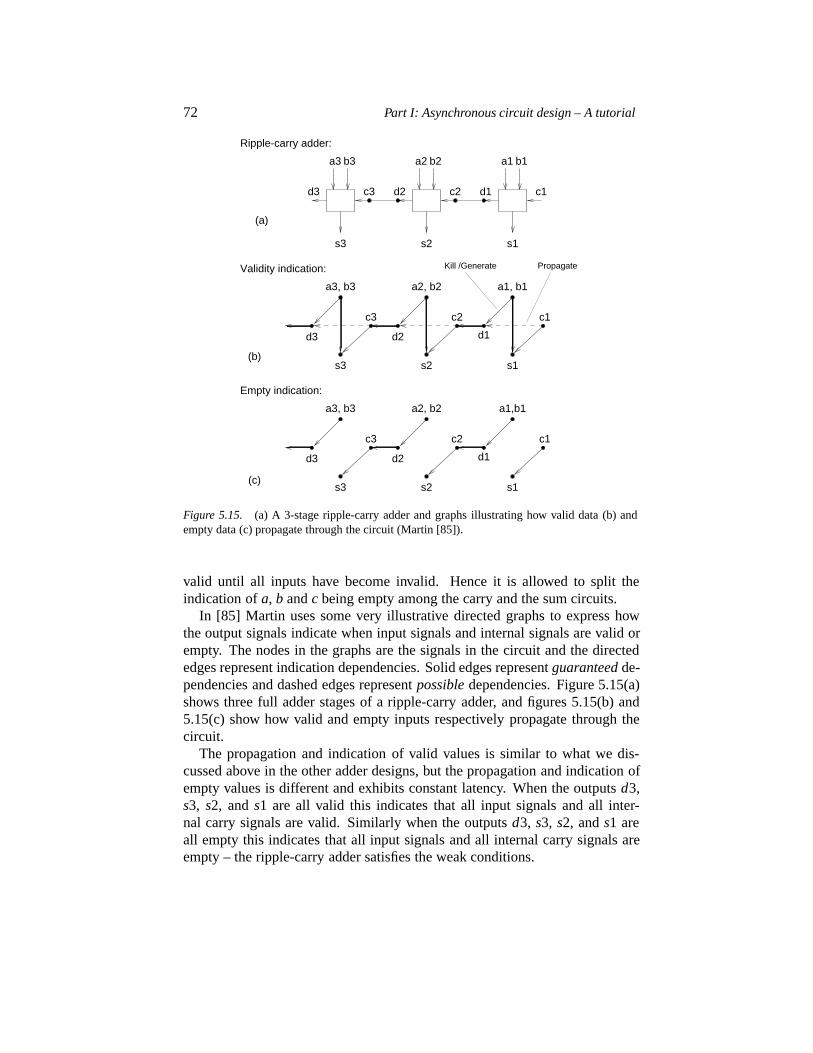
72 Part I: Asynchronous circuit design – A tutorial
s1
a1 b1
d1 c1c2
b2a2
d2
s2
b3a3
d3
s3
c3
c3
d2 d1
c2
d3
s3 s2 s1
c1
a3, b3 a1,b1
c3
d2 d1
c2
d3
s3 s2 s1
c1
a3, b3 a2, b2 a1, b1
a2, b2
(b)
(c)
(a)
Ripple-carry adder:
Validity indication:
Empty indication:
Kill /Generate Propagate
Figure 5.15. (a) A 3-stage ripple-carry adder and graphs illustrating how valid data (b) andempty data (c) propagate through the circuit (Martin [85]).
valid until all inputs have become invalid. Hence it is allowed to split theindication ofa, b andc being empty among the carry and the sum circuits.
In [85] Martin uses some very illustrative directed graphs to express howthe output signals indicate when input signals and internal signals are valid orempty. The nodes in the graphs are the signals in the circuit and the directededges represent indication dependencies. Solid edges representguaranteed de-pendencies and dashed edges representpossible dependencies. Figure 5.15(a)shows three full adder stages of a ripple-carry adder, and figures 5.15(b) and5.15(c) show how valid and empty inputs respectively propagate through thecircuit.
The propagation and indication of valid values is similar to what we dis-cussed above in the other adder designs, but the propagation and indication ofempty values is different and exhibits constant latency. When the outputsd3,s3, s2, ands1 are all valid this indicates that all input signals and all inter-nal carry signals are valid. Similarly when the outputsd3, s3, s2, ands1 areall empty this indicates that all input signals and all internal carry signals areempty – the ripple-carry adder satisfies the weak conditions.
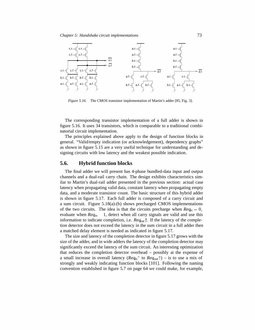
Chapter 5: Handshake circuit implementations 73
a.t
c.t
c.f
c.t
c.f
c.t
b.t
c.f
b.f
a.f
c.t
b.f
a.t
c.f
a.f
b.t
s.f
s.t
a.f
b.t
a.t
a.f
b.f
c.f
a.f b.f
d.f
b.f
a.f
b.t
a.t
a.t
b.t a.t b.t
c.t
d.t
b.f
Figure 5.16. The CMOS transistor implementation of Martin’s adder [85, Fig. 3].
The corresponding transistor implementation of a full adder is shown infigure 5.16. It uses 34 transistors, which is comparable to a traditional combi-natorial circuit implementation.
The principles explained above apply to the design of function blocks ingeneral. “Valid/empty indication (or acknowledgement), dependency graphs”as shown in figure 5.15 are a very useful technique for understanding and de-signing circuits with low latency and the weakest possible indication.
5.6. Hybrid function blocks
The final adder we will present has 4-phase bundled-data input and outputchannels and a dual-rail carry chain. The design exhibits characteristics sim-ilar to Martin’s dual-rail adder presented in the previous section: actual caselatency when propagating valid data, constant latency when propagating emptydata, and a moderate transistor count. The basic structure of this hybrid adderis shown in figure 5.17. Each full adder is composed of a carry circuit anda sum circuit. Figure 5.18(a)-(b) shows precharged CMOS implementationsof the two circuits. The idea is that the circuits precharge whenReqin � 0,evaluate whenReqin � 1, detect when all carry signals are valid and use thisinformation to indicate completion, i.e.Reqout. If the latency of the comple-tion detector does not exceed the latency in the sum circuit in a full adder thena matched delay element is needed as indicated in figure 5.17.
The size and latency of the completion detector in figure 5.17 grows with thesize of the adder, and in wide adders the latency of the completion detector maysignificantly exceed the latency of the sum circuit. An interesting optimizationthat reduces the completion detector overhead – possibly at the expense ofa small increase in overall latency (Reqin to Reqout) – is to use a mix ofstrongly and weakly indicating function blocks [101]. Following the namingconvention established in figure 5.7 on page 64 we could make, for example,
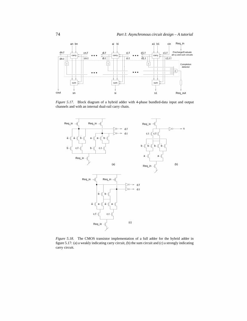
74 Part I: Asynchronous circuit design – A tutorial
C
Completiondetector
Precharge/Evaluateall cy and sum circuits
++ +
sumsum
sn si
sum
s1 Req_out
c1.t
d1.fci.f
ci.t d1.tdi.t
di.fdn.f
dn.t
c1.f
cin
cout
carry carry carry
bn bi b1a1aian
cn.f
cn.t
Req_in
Figure 5.17. Block diagram of a hybrid adder with 4-phase bundled-data input and outputchannels and with an internal dual-rail carry chain.
Req_inReq_in
Req_in
c.t
a baa
bb c.f
a b
d.t
d.f
Req_in
Req_in
a a
b b b b
c.t c.f
s
Req_in
d.t
d.f
(c)Req_in
c.f
a
Req_in
a
c.t
a
bb
a
(a) (b)
Figure 5.18. The CMOS transistor implementation of a full adder for the hybrid adder infigure 5.17: (a) a weakly indicating carry circuit, (b) the sum circuit and (c) a strongly indicatingcarry circuit.
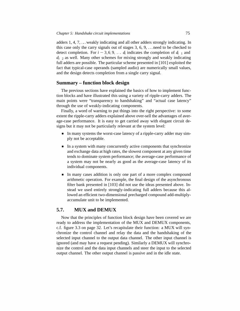
Chapter 5: Handshake circuit implementations 75
adders 1, 4, 7,� � �weakly indicating and all other adders strongly indicating. Inthis case only the carry signals out of stages 3, 6, 9,� � �need to be checked todetect completion. Fori � 3�6�9� � � � di indicates the completion ofdi�1 anddi�2 as well. Many other schemes for mixing strongly and weakly indicatingfull adders are possible. The particular scheme presented in [101] exploited thefact that typical-case operands (sampled audio) are numerically small values,and the design detects completion from a single carry signal.
Summary – function block design
The previous sections have explained the basics of how to implement func-tion blocks and have illustrated this using a variety of ripple-carry adders. Themain points were “transparency to handshaking” and “actual case latency”through the use of weakly-indicating components.
Finally, a word of warning to put things into the right perspective: to someextent the ripple-carry adders explained above over-sell the advantages of aver-age-case performance. It is easy to get carried away with elegant circuit de-signs but it may not be particularly relevant at the system level:
In many systems the worst-case latency of a ripple-carry adder may sim-ply not be acceptable.
In a system with many concurrently active components that synchronizeand exchange data at high rates, the slowest component at any given timetends to dominate system performance; the average-case performance ofa system may not be nearly as good as the average-case latency of itsindividual components.
In many cases addition is only one part of a more complex compoundarithmetic operation. For example, the final design of the asynchronousfilter bank presented in [103] did not use the ideas presented above. In-stead we used entirely strongly-indicating full adders because this al-lowed an efficient two-dimensional precharged compound add-multiply-accumulate unit to be implemented.
5.7. MUX and DEMUX
Now that the principles of function block design have been covered we areready to address the implementation of the MUX and DEMUX components,c.f. figure 3.3 on page 32. Let’s recapitulate their function: a MUX will syn-chronize the control channel and relay the data and the handshaking of theselected input channel to the output data channel. The other input channel isignored (and may have a request pending). Similarly a DEMUX will synchro-nize the control and the data input channels and steer the input to the selectedoutput channel. The other output channel is passive and in the idle state.
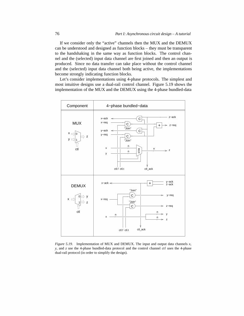
76 Part I: Asynchronous circuit design – A tutorial
If we consider only the “active” channels then the MUX and the DEMUXcan be understood and designed as function blocks – they must be transparentto the handshaking in the same way as function blocks. The control chan-nel and the (selected) input data channel are first joined and then an output isproduced. Since no data transfer can take place without the control channeland the (selected) input data channel both being active, the implementationsbecome strongly indicating function blocks.
Let’s consider implementations using 4-phase protocols. The simplest andmost intuitive designs use a dual-rail control channel. Figure 5.19 shows theimplementation of the MUX and the DEMUX using the 4-phase bundled-data
n
n
"Join"
"Join"
1
MUX
0
"Join"
1
z−ack
"Join"
y
DEMUX
y
z
ctl_ack
x
x−ack
Component 4−phase bundled−data
y−ack
y−ack0
y
y−req
z
ctl_ack
x−req
z−req
y−req
ctl.f ctl.t
n
ctl.f ctl.t
nn
MU
X
x
y
z−ack
z−req
Cx−ack
x−req
nctl
z
C
x
z
+
ctl
C
+
C
C
xC
Figure 5.19. Implementation of MUX and DEMUX. The input and output data channelsx,y, and z use the 4-phase bundled-data protocol and the control channelctl uses the 4-phasedual-rail protocol (in order to simplify the design).
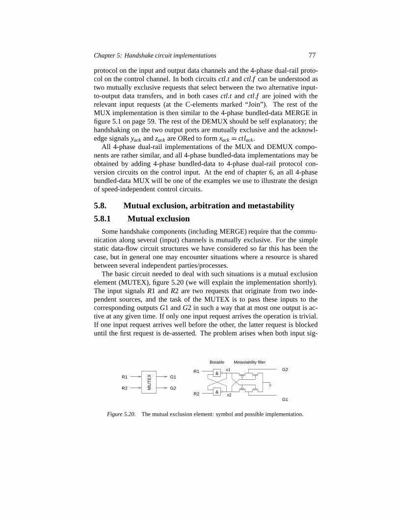
Chapter 5: Handshake circuit implementations 77
protocol on the input and output data channels and the 4-phase dual-rail proto-col on the control channel. In both circuitsctl�t andctl�f can be understood astwo mutually exclusive requests that select between the two alternative input-to-output data transfers, and in both casesctl�t and ctl�f are joined with therelevant input requests (at the C-elements marked “Join”). The rest of theMUX implementation is then similar to the 4-phase bundled-data MERGE infigure 5.1 on page 59. The rest of the DEMUX should be self explanatory; thehandshaking on the two output ports are mutually exclusive and the acknowl-edge signalsyack andzack are ORed to formxack � ctlack.
All 4-phase dual-rail implementations of the MUX and DEMUX compo-nents are rather similar, and all 4-phase bundled-data implementations may beobtained by adding 4-phase bundled-data to 4-phase dual-rail protocol con-version circuits on the control input. At the end of chapter 6, an all 4-phasebundled-data MUX will be one of the examples we use to illustrate the designof speed-independent control circuits.
5.8. Mutual exclusion, arbitration and metastability
5.8.1 Mutual exclusion
Some handshake components (including MERGE) require that the commu-nication along several (input) channels is mutually exclusive. For the simplestatic data-flow circuit structures we have considered so far this has been thecase, but in general one may encounter situations where a resource is sharedbetween several independent parties/processes.
The basic circuit needed to deal with such situations is a mutual exclusionelement (MUTEX), figure 5.20 (we will explain the implementation shortly).The input signalsR1 andR2 are two requests that originate from two inde-pendent sources, and the task of the MUTEX is to pass these inputs to thecorresponding outputsG1 andG2 in such a way that at most one output is ac-tive at any given time. If only one input request arrives the operation is trivial.If one input request arrives well before the other, the latter request is blockeduntil the first request is de-asserted. The problem arises when both input sig-
R1
R2
R1
R2
Bistable
&
&
G2
G1
G1
G2MU
TE
X
Metastability filter
x2
x1
Figure 5.20. The mutual exclusion element: symbol and possible implementation.
78 Part I: Asynchronous circuit design – A tutorial
nals are asserted at the same time. Then the MUTEX is required to make anarbitrary decision, and this is where metastability enters the picture.
The problem is exactly the same as when a synchronous circuit is exposedto an asynchronous input signal (one that does not satisfy set-up and hold timerequirements). For a clocked flip-flop that is used tosynchronize an asyn-chronous input signal, the question is whether the data signal made its tran-sition before or after the active edge of the clock. As with the MUTEX thequestion is again which signal transition occured first, and as with the MU-TEX a random decision is needed if the transition of the data signal coincideswith the active edge of the clock signal.
The fundamental problem in a MUTEX and in a synchronizer flip-flop isthat we are dealing with a bi-stable circuit that receives requests to enter eachof its two stable states at the same time. This will cause the circuit to enter ametastable state in which it may stay for an unbounded length of time beforerandomly settling in one of its stable states. The problem of synchronizationis covered in most textbooks on digital design and VLSI, and the analysis ofmetastability that is presented in these textbooks applies to our MUTEX com-ponent as well. A selection of references is: [95, sect. 9.4] [53, sect. 5.4 and6.5] [151, sect. 5.5.7] [115, sect. 6.2.2 and 9.4-5] [150, sect. 8.9].
For the synchronous designer the problem is that metastability may per-sist beyond the time interval that has been allocated to recover from potentialmetastability. It is simply not possible to obtain a decision within a boundedlength of time. The asynchronous designer, on the other hand, will eventuallyobtain a decision, but there is no upper limit on the time he will have to waitfor the answer. In [22] the terms “time safe” and “value safe” are introducedto denote and classify these two situations.
A possible implementation of the MUTEX, as shown in figure 5.20, in-volves a pair of cross coupled NAND gates and a metastability filter. The crosscoupled NAND gates enable one input to block the other. If both inputs areasserted at the same time, the circuit becomes metastable with both signalsx1 andx2 halfway between supply and ground. The metastability filter pre-vents these undefined values from propagating to the outputs;G1 andG2 areboth kept low until signalsx1 andx2 differ by more than a transistor thresholdvoltage.
The metastability filter in figure 5.20 is a CMOS transistor-level implemen-tation from [83]. An NMOS predecessor of this circuit appeared in [121].Gate-level implementations are also possible: the metastability filter can beimplemented using two buffers whose logic thresholds have been made partic-ularly high (or low) by “trimming” the strengths of the pull-up and pull-downtransistor paths ([151, section 2.3]). For example, a 4-input NAND gate withall its inputs tied together implements a buffer with a particularly high logic
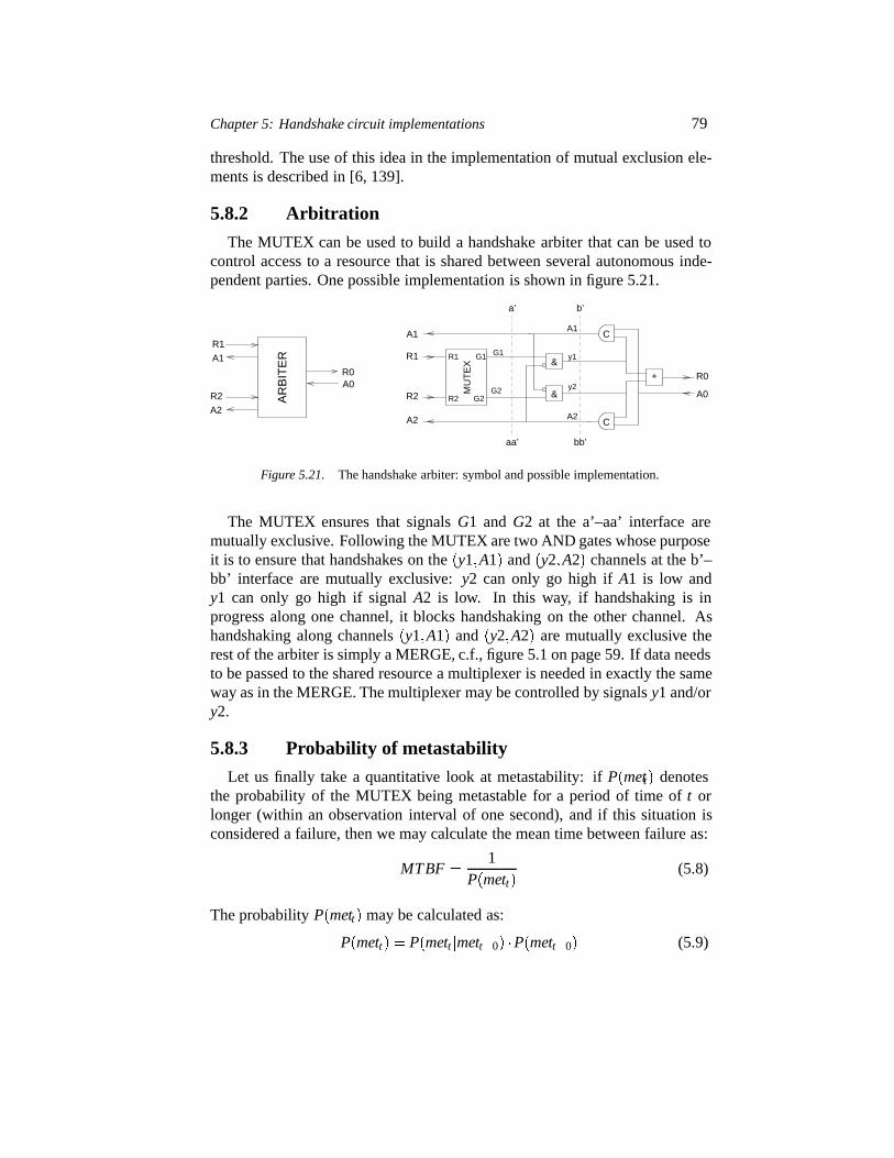
Chapter 5: Handshake circuit implementations 79
threshold. The use of this idea in the implementation of mutual exclusion ele-ments is described in [6, 139].
5.8.2 Arbitration
The MUTEX can be used to build a handshake arbiter that can be used tocontrol access to a resource that is shared between several autonomous inde-pendent parties. One possible implementation is shown in figure 5.21.
&
&
C
C
R0A0
R1
A1
R2
A2
AR
BIT
ER
+ R0
A0
y1
y2
G1
MU
TE
X
R2 G2
G1R1
A1
R1
R2
A2
G2
A1
A2
a’
aa’
b’
bb’
Figure 5.21. The handshake arbiter: symbol and possible implementation.
The MUTEX ensures that signalsG1 andG2 at the a’–aa’ interface aremutually exclusive. Following the MUTEX are two AND gates whose purposeit is to ensure that handshakes on the�y1�A1� and�y2�A2� channels at the b’–bb’ interface are mutually exclusive:y2 can only go high ifA1 is low andy1 can only go high if signalA2 is low. In this way, if handshaking is inprogress along one channel, it blocks handshaking on the other channel. Ashandshaking along channels�y1�A1� and�y2�A2� are mutually exclusive therest of the arbiter is simply a MERGE, c.f., figure 5.1 on page 59. If data needsto be passed to the shared resource a multiplexer is needed in exactly the sameway as in the MERGE. The multiplexer may be controlled by signalsy1 and/ory2.
5.8.3 Probability of metastability
Let us finally take a quantitative look at metastability: ifP�mett� denotesthe probability of the MUTEX being metastable for a period of time oft orlonger (within an observation interval of one second), and if this situation isconsidered a failure, then we may calculate the mean time between failure as:
MTBF �1
P�mett�(5.8)
The probabilityP�mett� may be calculated as:
P�mett� � P�mett �mett�0� �P�mett�0� (5.9)
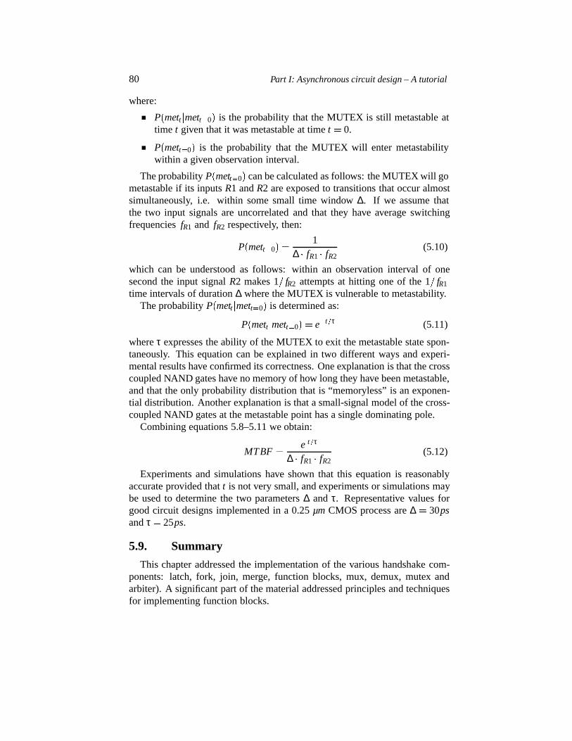
80 Part I: Asynchronous circuit design – A tutorial
where:
P�mett �mett�0� is the probability that the MUTEX is still metastable attime t given that it was metastable at timet � 0.
P�mett�0� is the probability that the MUTEX will enter metastabilitywithin a given observation interval.
The probabilityP�mett�0� can be calculated as follows: the MUTEX will gometastable if its inputsR1 andR2 are exposed to transitions that occur almostsimultaneously, i.e. within some small time window∆. If we assume thatthe two input signals are uncorrelated and that they have average switchingfrequenciesfR1 and fR2 respectively, then:
P�mett�0� �1
∆ � fR1 � fR2(5.10)
which can be understood as follows: within an observation interval of onesecond the input signalR2 makes 1� fR2 attempts at hitting one of the 1� fR1
time intervals of duration∆ where the MUTEX is vulnerable to metastability.The probabilityP�mett �mett�0� is determined as:
P�mett �mett�0� � e�t�τ (5.11)
whereτ expresses the ability of the MUTEX to exit the metastable state spon-taneously. This equation can be explained in two different ways and experi-mental results have confirmed its correctness. One explanation is that the crosscoupled NAND gates have no memory of how long they have been metastable,and that the only probability distribution that is “memoryless” is an exponen-tial distribution. Another explanation is that a small-signal model of the cross-coupled NAND gates at the metastable point has a single dominating pole.
Combining equations 5.8–5.11 we obtain:
MTBF �e t�τ
∆ � fR1 � fR2(5.12)
Experiments and simulations have shown that this equation is reasonablyaccurate provided thatt is not very small, and experiments or simulations maybe used to determine the two parameters∆ andτ. Representative values forgood circuit designs implemented in a 0.25µm CMOS process are∆ � 30psandτ � 25ps.
5.9. Summary
This chapter addressed the implementation of the various handshake com-ponents: latch, fork, join, merge, function blocks, mux, demux, mutex andarbiter). A significant part of the material addressed principles and techniquesfor implementing function blocks.
Chapter 6
SPEED-INDEPENDENT CONTROL CIRCUITS
This chapter provides an introduction to the design of asynchronous sequen-tial circuits and explains in detail one well-developed specification and synthe-sis method: the synthesis of speed-independent control circuits from signaltransition graph specifications.
6.1. Introduction
Over time many different formalisms and theories have been proposed forthe design of asynchronous control circuits (e.g. sequential circuits or statemachines). The multitude of approaches arises from the combination of: (a)different specification formalisms, (b) different assumptions about delay mod-els for gates and wires, and (c) different assumptions about the interactionbetween the circuit and its environment. Full coverage of the topic is far be-yond the scope of this book. Instead we will first present some of the basicassumptions and characteristics of the various design methods and give point-ers to relevant literature and then we will explain in detail one method: thedesign of speed-independent circuits from signal transition graphs – a methodthat is supported by a well-developed public domain tool, Petrify.
A good starting point for further reading is a book by Myers [95]. It providesin-depth coverage of the various formalisms, methods, and theories for thedesign of asynchronous sequential circuits and it provides a comprehensivelist of references.
6.1.1 Asynchronous sequential circuits
To start the discussion figure 6.1 shows a generic synchronous sequentialcircuit and two alternative asynchronous control circuits: a Huffman style fun-damental mode circuit with buffers (delay elements) in the feedback signals,and a Muller style input-output mode circuit with wires in the feedback path.
The synchronous circuit is composed of a set of registers holding the currentstate and a combinational logic circuit that computes the output signals and thenext state signals. When the clock ticks the next state signals are copied into theregisters thus becoming the current state. Reliable operation only requires that
81
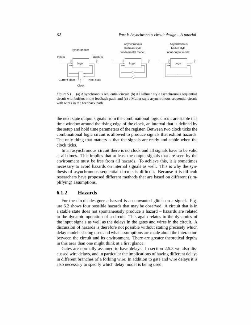
82 Part I: Asynchronous circuit design – A tutorial
Synchronous:
Clock
Current state Next state
Asynchronous
Huffman style
fundamental mode:
Muller style
Asynchronous
input-output mode:
Logic LogicLogic
Inputs Outputs
Figure 6.1. (a) A synchronous sequential circuit. (b) A Huffman style asynchronous sequentialcircuit with buffers in the feedback path, and (c) a Muller style asynchronous sequential circuitwith wires in the feedback path.
the next state output signals from the combinational logic circuit are stable in atime window around the rising edge of the clock, an interval that is defined bythe setup and hold time parameters of the register. Between two clock ticks thecombinational logic circuit is allowed to produce signals that exhibit hazards.The only thing that matters is that the signals are ready and stable when theclock ticks.
In an asynchronous circuit there is no clock and all signals have to be validat all times. This implies that at least the output signals that are seen by theenvironment must be free from all hazards. To achieve this, it is sometimesnecessary to avoid hazards on internal signals as well. This is why the syn-thesis of asynchronous sequential circuits is difficult. Because it is difficultresearchers have proposed different methods that are based on different (sim-plifying) assumptions.
6.1.2 Hazards
For the circuit designer a hazard is an unwanted glitch on a signal. Fig-ure 6.2 shows four possible hazards that may be observed. A circuit that is ina stable state does not spontaneously produce a hazard – hazards are relatedto the dynamic operation of a circuit. This again relates to the dynamics ofthe input signals as well as the delays in the gates and wires in the circuit. Adiscussion of hazards is therefore not possible without stating precisely whichdelay model is being used and what assumptions are made about the interactionbetween the circuit and its environment. There are greater theoretical depthsin this area than one might think at a first glance.
Gates are normally assumed to have delays. In section 2.5.3 we also dis-cussed wire delays, and in particular the implications of having different delaysin different branches of a forking wire. In addition to gate and wire delays it isalso necessary to specify which delay model is being used.
Chapter 6: Speed-independent control circuits 83
Static-1 hazard:
Static-0 hazard:
1
00
1
1 0 11 0
0 1 1 00
1
0
0
1
1
0
Desired signal Actual signal
Dynamic-10 hazard:
Dynamic-01 hazard:
Figure 6.2. Possible hazards that may be observed on a signal.
6.1.3 Delay models
A pure delay that simply shifts any signal waveform later in time is perhapswhat first comes to mind. In the hardware description language VHDL this iscalled atransport delay. It is, however, not a very realistic model as it impliesthat the gates and wires have infinitely high bandwidth. A more realistic delaymodel is theinertial delay model. In addition to the time shifting of a signalwaveform, an inertial delay suppresses short pulses. In the inertial delay modelused in VHDL two parameters are specified, thedelay time and thereject time,and pulses shorter than the reject time are filtered out. The inertial delay modelis the default delay model used in VHDL.
These two fundamental delay models come in several flavours depending onhow the delay time parameter is specified. The simplest is afixed delay wherethe delay is a constant. An alternative is amin-max delay where the delay isunknown but within a lower and upper bound:tmin � tdelay � tmax. A morepessimistic model is theunbounded delay where delays are positive (i.e. notzero), unknown and unbounded from above: 0� tdelay � ∞. This is the delaymodel that is used for gates in speed-independent circuits.
It is intuitive that the inertial delay model and the min-max delay modelboth have properties that help filter out some potential hazards.
6.1.4 Fundamental mode and input-output mode
In addition to the delays in the gates and wires, it is also necessary to for-malize the interaction between the circuit being designed and its environment.Again, strong assumptions may simplify the design of the circuit. The designmethods that have been proposed over time all have their roots in one of thefollowing assumptions:
Fundamental mode: The circuit is assumed to be in a state where all inputsignals, internal signals, and output signals are stable. In such a sta-ble state the environment is allowed to change one input signal. After
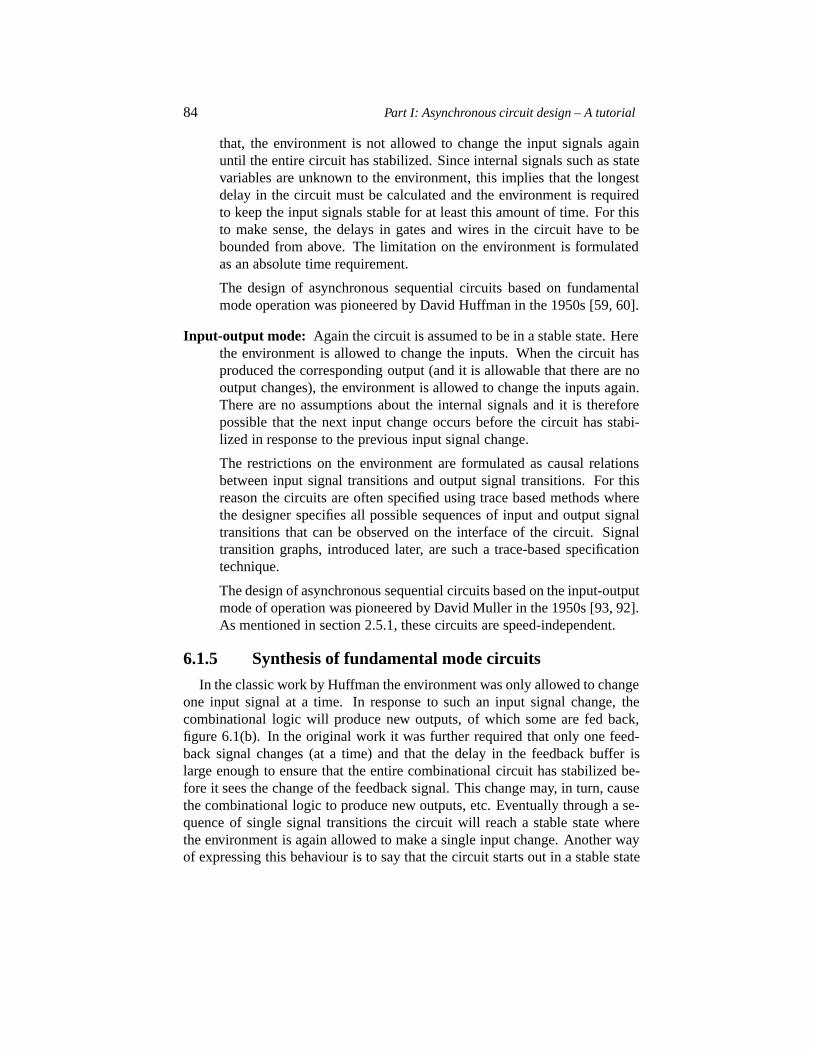
84 Part I: Asynchronous circuit design – A tutorial
that, the environment is not allowed to change the input signals againuntil the entire circuit has stabilized. Since internal signals such as statevariables are unknown to the environment, this implies that the longestdelay in the circuit must be calculated and the environment is requiredto keep the input signals stable for at least this amount of time. For thisto make sense, the delays in gates and wires in the circuit have to bebounded from above. The limitation on the environment is formulatedas an absolute time requirement.
The design of asynchronous sequential circuits based on fundamentalmode operation was pioneered by David Huffman in the 1950s [59, 60].
Input-output mode: Again the circuit is assumed to be in a stable state. Herethe environment is allowed to change the inputs. When the circuit hasproduced the corresponding output (and it is allowable that there are nooutput changes), the environment is allowed to change the inputs again.There are no assumptions about the internal signals and it is thereforepossible that the next input change occurs before the circuit has stabi-lized in response to the previous input signal change.
The restrictions on the environment are formulated as causal relationsbetween input signal transitions and output signal transitions. For thisreason the circuits are often specified using trace based methods wherethe designer specifies all possible sequences of input and output signaltransitions that can be observed on the interface of the circuit. Signaltransition graphs, introduced later, are such a trace-based specificationtechnique.
The design of asynchronous sequential circuits based on the input-outputmode of operation was pioneered by David Muller in the 1950s [93, 92].As mentioned in section 2.5.1, these circuits are speed-independent.
6.1.5 Synthesis of fundamental mode circuits
In the classic work by Huffman the environment was only allowed to changeone input signal at a time. In response to such an input signal change, thecombinational logic will produce new outputs, of which some are fed back,figure 6.1(b). In the original work it was further required that only one feed-back signal changes (at a time) and that the delay in the feedback buffer islarge enough to ensure that the entire combinational circuit has stabilized be-fore it sees the change of the feedback signal. This change may, in turn, causethe combinational logic to produce new outputs, etc. Eventually through a se-quence of single signal transitions the circuit will reach a stable state wherethe environment is again allowed to make a single input change. Another wayof expressing this behaviour is to say that the circuit starts out in a stable state
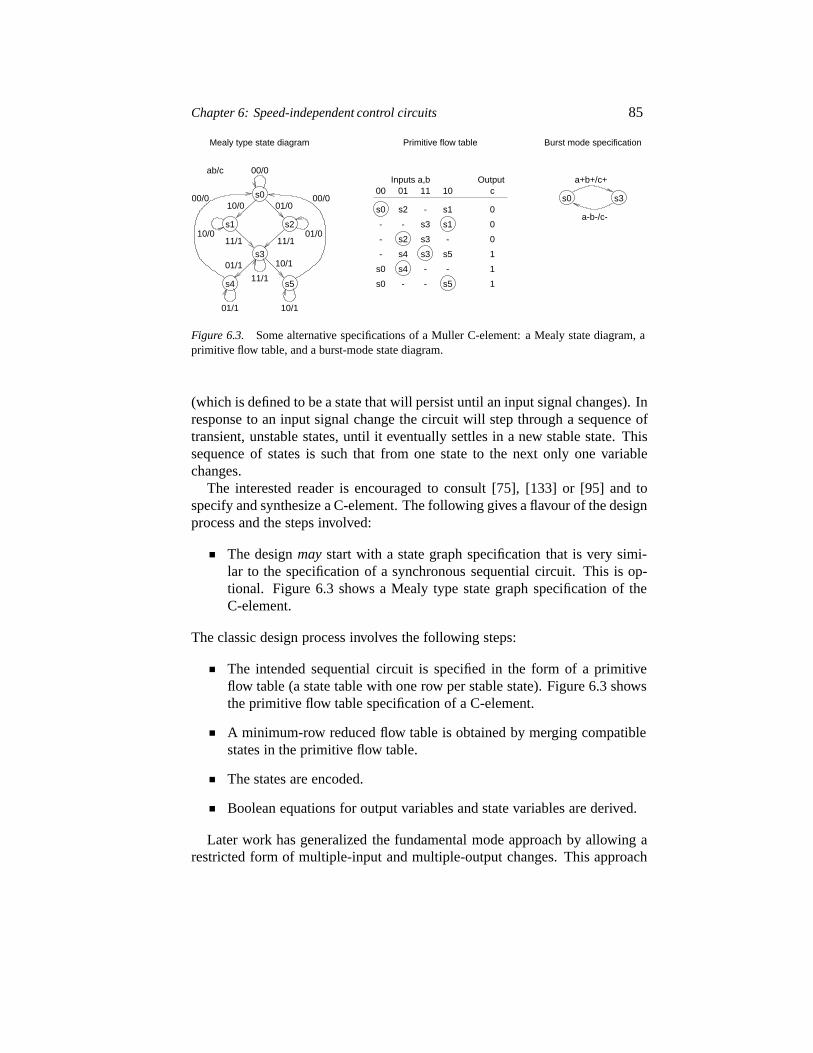
Chapter 6: Speed-independent control circuits 85
s0 00 01 11 c10Inputs a,b Output
s0 s1s2 - 0
s1s3--
s2 s3 --
s3 s5s4-
s4s0
s5s0 - -
0
0
1
1
1
- -
s1 s2
s3
s4 s5
00/0
00/0
11/110/0
11/1
10/0 01/0
01/0
Primitive flow tableMealy type state diagram
ab/c
01/1 10/1
01/1 10/1
00/0
11/1
Burst mode specification
s0
a+b+/c+
a-b-/c-
s3
Figure 6.3. Some alternative specifications of a Muller C-element: a Mealy state diagram, aprimitive flow table, and a burst-mode state diagram.
(which is defined to be a state that will persist until an input signal changes). Inresponse to an input signal change the circuit will step through a sequence oftransient, unstable states, until it eventually settles in a new stable state. Thissequence of states is such that from one state to the next only one variablechanges.
The interested reader is encouraged to consult [75], [133] or [95] and tospecify and synthesize a C-element. The following gives a flavour of the designprocess and the steps involved:
The designmay start with a state graph specification that is very simi-lar to the specification of a synchronous sequential circuit. This is op-tional. Figure 6.3 shows a Mealy type state graph specification of theC-element.
The classic design process involves the following steps:
The intended sequential circuit is specified in the form of a primitiveflow table (a state table with one row per stable state). Figure 6.3 showsthe primitive flow table specification of a C-element.
A minimum-row reduced flow table is obtained by merging compatiblestates in the primitive flow table.
The states are encoded.
Boolean equations for output variables and state variables are derived.
Later work has generalized the fundamental mode approach by allowing arestricted form of multiple-input and multiple-output changes. This approach
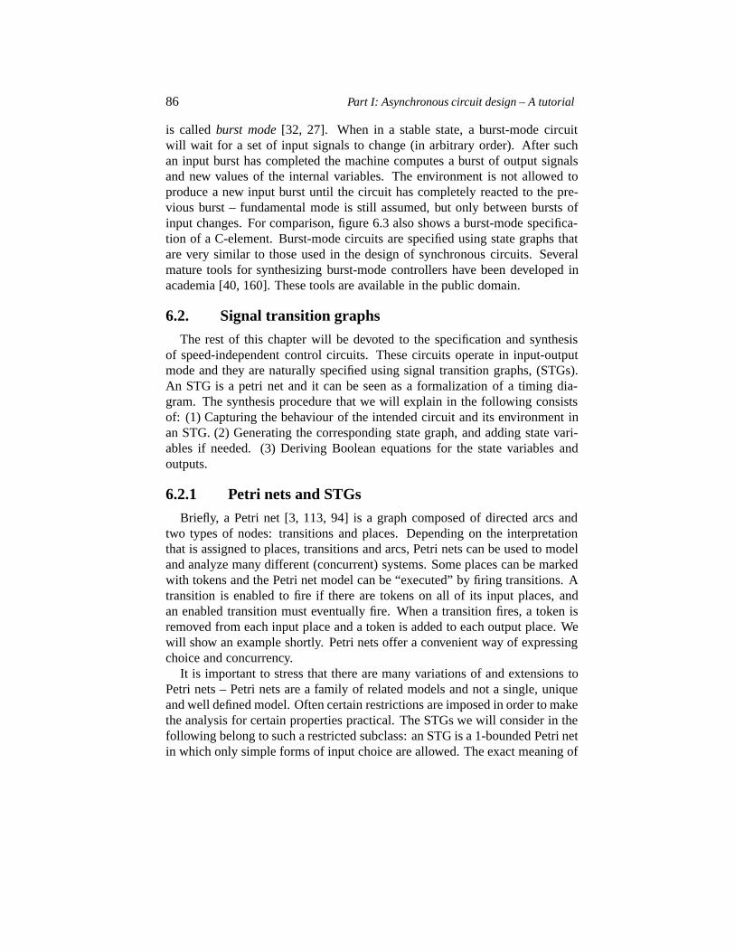
86 Part I: Asynchronous circuit design – A tutorial
is calledburst mode [32, 27]. When in a stable state, a burst-mode circuitwill wait for a set of input signals to change (in arbitrary order). After suchan input burst has completed the machine computes a burst of output signalsand new values of the internal variables. The environment is not allowed toproduce a new input burst until the circuit has completely reacted to the pre-vious burst – fundamental mode is still assumed, but only between bursts ofinput changes. For comparison, figure 6.3 also shows a burst-mode specifica-tion of a C-element. Burst-mode circuits are specified using state graphs thatare very similar to those used in the design of synchronous circuits. Severalmature tools for synthesizing burst-mode controllers have been developed inacademia [40, 160]. These tools are available in the public domain.
6.2. Signal transition graphs
The rest of this chapter will be devoted to the specification and synthesisof speed-independent control circuits. These circuits operate in input-outputmode and they are naturally specified using signal transition graphs, (STGs).An STG is a petri net and it can be seen as a formalization of a timing dia-gram. The synthesis procedure that we will explain in the following consistsof: (1) Capturing the behaviour of the intended circuit and its environment inan STG. (2) Generating the corresponding state graph, and adding state vari-ables if needed. (3) Deriving Boolean equations for the state variables andoutputs.
6.2.1 Petri nets and STGs
Briefly, a Petri net [3, 113, 94] is a graph composed of directed arcs andtwo types of nodes: transitions and places. Depending on the interpretationthat is assigned to places, transitions and arcs, Petri nets can be used to modeland analyze many different (concurrent) systems. Some places can be markedwith tokens and the Petri net model can be “executed” by firing transitions. Atransition is enabled to fire if there are tokens on all of its input places, andan enabled transition must eventually fire. When a transition fires, a token isremoved from each input place and a token is added to each output place. Wewill show an example shortly. Petri nets offer a convenient way of expressingchoice and concurrency.
It is important to stress that there are many variations of and extensions toPetri nets – Petri nets are a family of related models and not a single, uniqueand well defined model. Often certain restrictions are imposed in order to makethe analysis for certain properties practical. The STGs we will consider in thefollowing belong to such a restricted subclass: an STG is a 1-bounded Petri netin which only simple forms of input choice are allowed. The exact meaning of
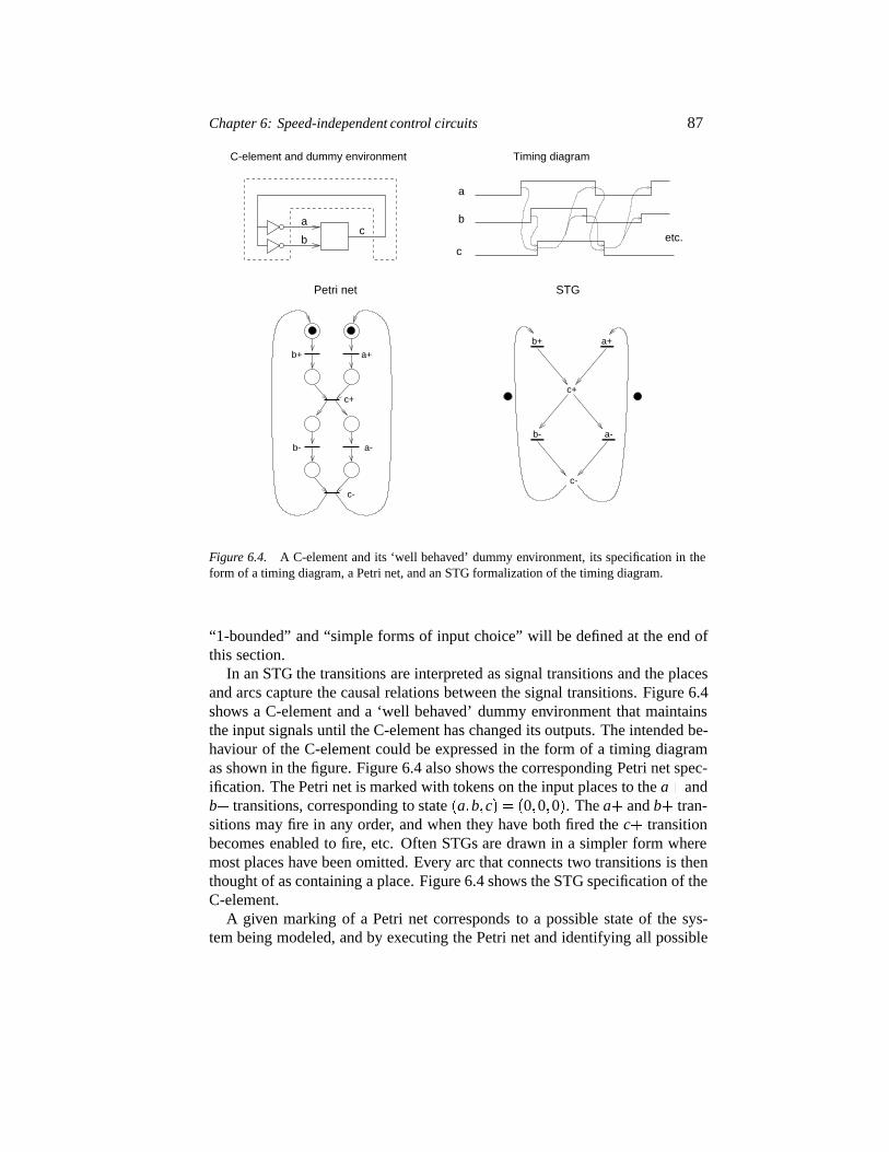
Chapter 6: Speed-independent control circuits 87
Timing diagramC-element and dummy environment
a
b
cetc.
ac
b
b+
b-
a+
a-
c-
c+
STG
b+
c+
b-
c-
a+
a-
Petri net
Figure 6.4. A C-element and its ‘well behaved’ dummy environment, its specification in theform of a timing diagram, a Petri net, and an STG formalization of the timing diagram.
“1-bounded” and “simple forms of input choice” will be defined at the end ofthis section.
In an STG the transitions are interpreted as signal transitions and the placesand arcs capture the causal relations between the signal transitions. Figure 6.4shows a C-element and a ‘well behaved’ dummy environment that maintainsthe input signals until the C-element has changed its outputs. The intended be-haviour of the C-element could be expressed in the form of a timing diagramas shown in the figure. Figure 6.4 also shows the corresponding Petri net spec-ification. The Petri net is marked with tokens on the input places to thea� andb� transitions, corresponding to state�a�b�c� � �0�0�0�. Thea� andb� tran-sitions may fire in any order, and when they have both fired thec� transitionbecomes enabled to fire, etc. Often STGs are drawn in a simpler form wheremost places have been omitted. Every arc that connects two transitions is thenthought of as containing a place. Figure 6.4 shows the STG specification of theC-element.
A given marking of a Petri net corresponds to a possible state of the sys-tem being modeled, and by executing the Petri net and identifying all possible
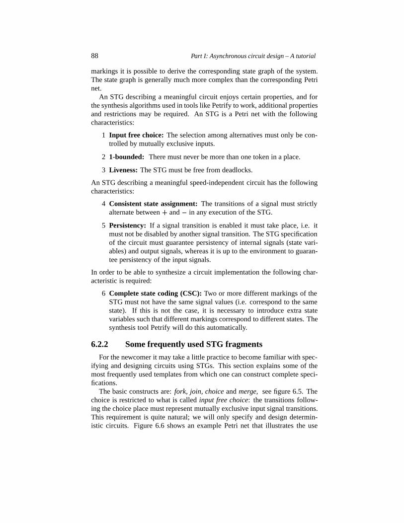
88 Part I: Asynchronous circuit design – A tutorial
markings it is possible to derive the corresponding state graph of the system.The state graph is generally much more complex than the corresponding Petrinet.
An STG describing a meaningful circuit enjoys certain properties, and forthe synthesis algorithms used in tools like Petrify to work, additional propertiesand restrictions may be required. An STG is a Petri net with the followingcharacteristics:
1 Input free choice: The selection among alternatives must only be con-trolled by mutually exclusive inputs.
2 1-bounded: There must never be more than one token in a place.
3 Liveness:The STG must be free from deadlocks.
An STG describing a meaningful speed-independent circuit has the followingcharacteristics:
4 Consistent state assignment:The transitions of a signal must strictlyalternate between� and� in any execution of the STG.
5 Persistency: If a signal transition is enabled it must take place, i.e. itmust not be disabled by another signal transition. The STG specificationof the circuit must guarantee persistency of internal signals (state vari-ables) and output signals, whereas it is up to the environment to guaran-tee persistency of the input signals.
In order to be able to synthesize a circuit implementation the following char-acteristic is required:
6 Complete state coding (CSC):Two or more different markings of theSTG must not have the same signal values (i.e. correspond to the samestate). If this is not the case, it is necessary to introduce extra statevariables such that different markings correspond to different states. Thesynthesis tool Petrify will do this automatically.
6.2.2 Some frequently used STG fragments
For the newcomer it may take a little practice to become familiar with spec-ifying and designing circuits using STGs. This section explains some of themost frequently used templates from which one can construct complete speci-fications.
The basic constructs are:fork, join, choice andmerge, see figure 6.5. Thechoice is restricted to what is calledinput free choice: the transitions follow-ing the choice place must represent mutually exclusive input signal transitions.This requirement is quite natural; we will only specify and design determin-istic circuits. Figure 6.6 shows an example Petri net that illustrates the use
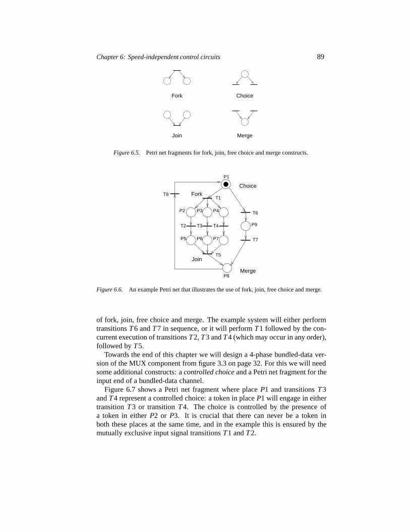
Chapter 6: Speed-independent control circuits 89
Fork
Join
Choice
Merge
Figure 6.5. Petri net fragments for fork, join, free choice and merge constructs.
P9
T7
P8
P7
P2
P6P5
P4P3
P1
T3T2
T8
T6
T5
T1Fork
Join
Merge
Choice
T4
Figure 6.6. An example Petri net that illustrates the use of fork, join, free choice and merge.
of fork, join, free choice and merge. The example system will either performtransitionsT 6 andT7 in sequence, or it will performT 1 followed by the con-current execution of transitionsT2, T3 andT4 (which may occur in any order),followed byT5.
Towards the end of this chapter we will design a 4-phase bundled-data ver-sion of the MUX component from figure 3.3 on page 32. For this we will needsome additional constructs: acontrolled choice and a Petri net fragment for theinput end of a bundled-data channel.
Figure 6.7 shows a Petri net fragment where placeP1 and transitionsT3andT4 represent a controlled choice: a token in placeP1 will engage in eithertransitionT3 or transitionT4. The choice is controlled by the presence ofa token in eitherP2 or P3. It is crucial that there can never be a token inboth these places at the same time, and in the example this is ensured by themutually exclusive input signal transitionsT1 andT2.
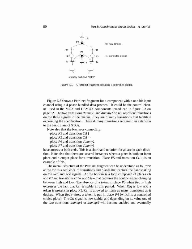
90 Part I: Asynchronous circuit design – A tutorial
T2
T5
P1
T0
T1
P2 P1: Controlled Choice
Mutually exclusive "paths"
T3 T4
P3
P0P0: Free Choice
Figure 6.7. A Petri net fragment including a controlled choice.
Figure 6.8 shows a Petri net fragment for a component with a one-bit inputchannel using a 4-phase bundled-data protocol. It could be the control chan-nel used in the MUX and DEMUX components introduced in figure 3.3 onpage 32. The two transitionsdummy1 anddummy2 do not represent transitionson the three signals in the channel, they are dummy transitions that facilitateexpressing the specification. These dummy transitions represent an extensionto the basic class of STGs.
Note also that the four arcs connecting:placeP5 and transitionCtl�placeP5 and transitionCtl�placeP6 and transitiondummy2placeP7 and transitiondummy1
have arrows at both ends. This is a shorthand notation for an arc in each direc-tion. Note also that there are several instances where a place is both an inputplace and a output place for a transition. PlaceP5 and transitionCtl� is anexample of this.
The overall structure of the Petri net fragment can be understood as follows:at the top is a sequence of transitions and places that capture the handshakingon theReq andAck signals. At the bottom is a loop composed of placesP6andP7 and transitionsCtl� andCtl� that captures the control signal changingbetween high and low. The absence of a token in placeP5 whenReq is highexpresses the fact thatCtl is stable in this period. WhenReq is low and atoken is present in placeP5, Ctl is allowed to make as many transitions as itdesires. WhenReq� fires, a token is put in placeP4 (which is a controlledchoice place). TheCtl signal is now stable, and depending on its value one ofthe two transitionsdummy1 or dummy2 will become enabled and eventually
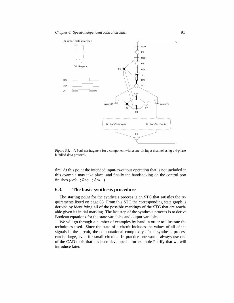
Chapter 6: Speed-independent control circuits 91
Req
Ack
Ctl
Bundled data interface
Ctl Req/Ack
Ctl−
Ctl+
Ack+
Req−
Ack−
Do the "Ctl=0" action Do the "Ctl=1" action
dummy1dummy2
P1
P2
P6 P7
Req+
P3
P4
P5
P0
Figure 6.8. A Petri net fragment for a component with a one-bit input channel using a 4-phasebundled-data protocol.
fire. At this point the intended input-to-output operation that is not included inthis example may take place, and finally the handshaking on the control portfinishes (Ack�; Req�; Ack�).
6.3. The basic synthesis procedure
The starting point for the synthesis process is an STG that satisfies the re-quirements listed on page 88. From this STG the corresponding state graph isderived by identifying all of the possible markings of the STG that are reach-able given its initial marking. The last step of the synthesis process is to deriveBoolean equations for the state variables and output variables.
We will go through a number of examples by hand in order to illustrate thetechniques used. Since the state of a circuit includes the values of all of thesignals in the circuit, the computational complexity of the synthesis processcan be large, even for small circuits. In practice one would always use oneof the CAD tools that has been developed – for example Petrify that we willintroduce later.
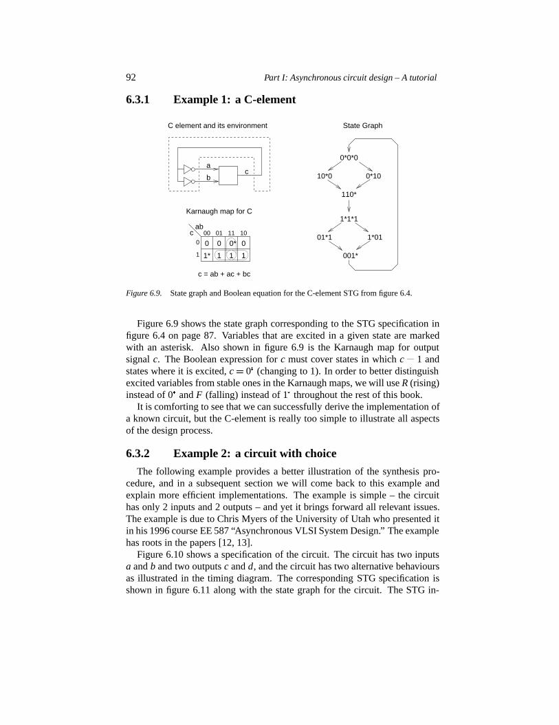
92 Part I: Asynchronous circuit design – A tutorial
6.3.1 Example 1: a C-element
cab
00 01 10
0
1
0 0
11
0* 0
1* 1 1 1
c = ab + ac + bc
C element and its environment State Graph
Karnaugh map for C
0*0*0
10*0 0*10
110*
01*1 1*01
001*
1*1*1
ac
b
Figure 6.9. State graph and Boolean equation for the C-element STG from figure 6.4.
Figure 6.9 shows the state graph corresponding to the STG specification infigure 6.4 on page 87. Variables that are excited in a given state are markedwith an asterisk. Also shown in figure 6.9 is the Karnaugh map for outputsignalc. The Boolean expression forc must cover states in whichc � 1 andstates where it is excited,c � 0� (changing to 1). In order to better distinguishexcited variables from stable ones in the Karnaugh maps, we will useR (rising)instead of 0� andF (falling) instead of 1� throughout the rest of this book.
It is comforting to see that we can successfully derive the implementation ofa known circuit, but the C-element is really too simple to illustrate all aspectsof the design process.
6.3.2 Example 2: a circuit with choice
The following example provides a better illustration of the synthesis pro-cedure, and in a subsequent section we will come back to this example andexplain more efficient implementations. The example is simple – the circuithas only 2 inputs and 2 outputs – and yet it brings forward all relevant issues.The example is due to Chris Myers of the University of Utah who presented itin his 1996 course EE 587 “Asynchronous VLSI System Design.” The examplehas roots in the papers [12, 13].
Figure 6.10 shows a specification of the circuit. The circuit has two inputsa andb and two outputsc andd, and the circuit has two alternative behavioursas illustrated in the timing diagram. The corresponding STG specification isshown in figure 6.11 along with the state graph for the circuit. The STG in-
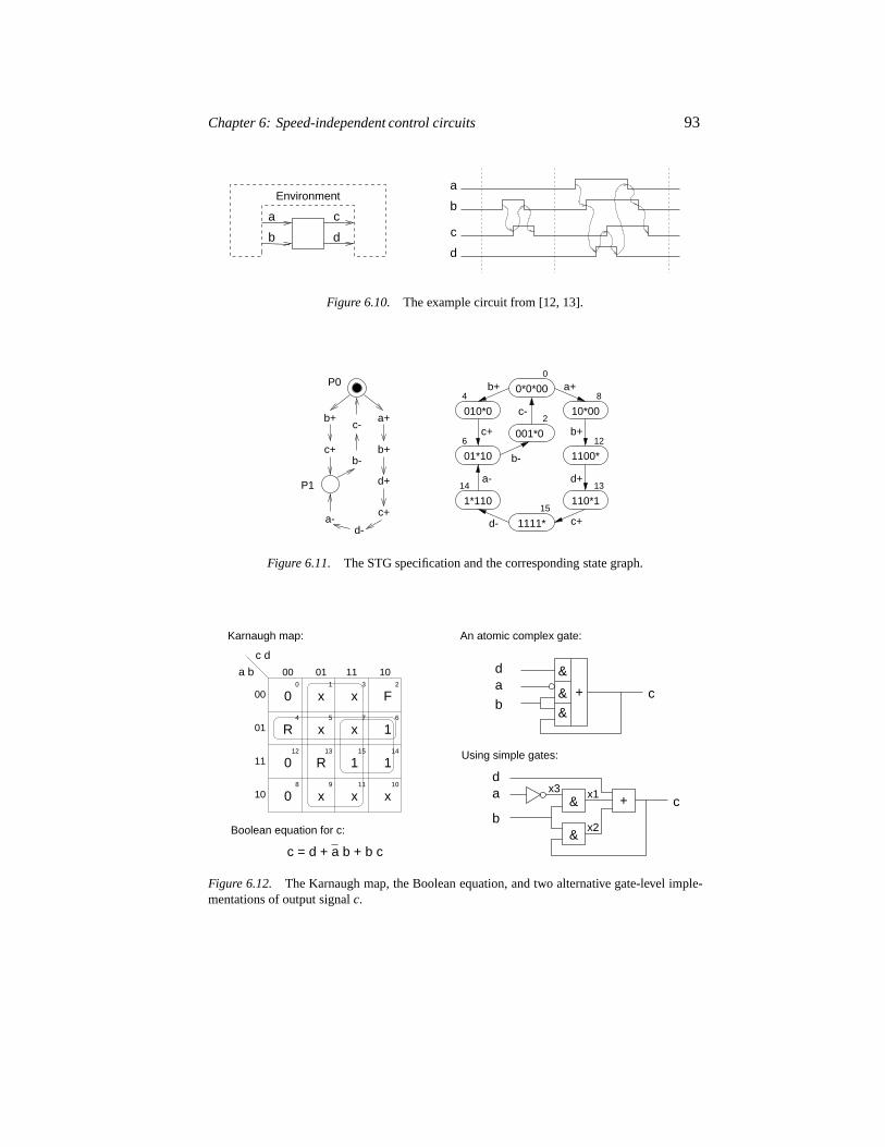
Chapter 6: Speed-independent control circuits 93
Environment
a
b
c
d
a
b
c
d
Figure 6.10. The example circuit from [12, 13].
001*0
10*00
1100*
110*1
1111*
0*0*00
1*110
01*10
010*0
14
6
4
0
8
12
2
15
13
a+
b+
d+
c+d-
c-
b-
b+
c+
a-
b+ a+
c+ b+
d+
c+a-
b-
c-
d-
P1
P0
Figure 6.11. The STG specification and the corresponding state graph.
x3
x2
2
6
14
10
3
7
15
118 9
12 13
54
0 1
10
11
01
10110100
00
c d
a b
0
0 x x x
x x
x x 1
0 1 1
R
R
F
+
&
&
c = d + a b + b c
da
bc
&
&
&
+
b
ad
c
Karnaugh map:
Boolean equation for c:
An atomic complex gate:
Using simple gates:
x1
Figure 6.12. The Karnaugh map, the Boolean equation, and two alternative gate-level imple-mentations of output signalc.
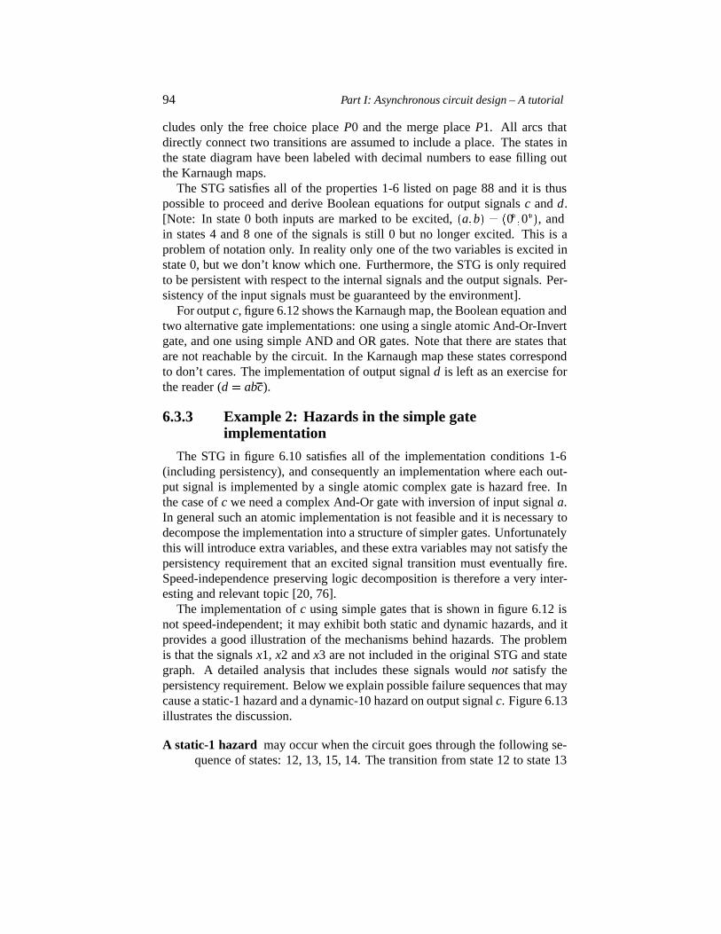
94 Part I: Asynchronous circuit design – A tutorial
cludes only the free choice placeP0 and the merge placeP1. All arcs thatdirectly connect two transitions are assumed to include a place. The states inthe state diagram have been labeled with decimal numbers to ease filling outthe Karnaugh maps.
The STG satisfies all of the properties 1-6 listed on page 88 and it is thuspossible to proceed and derive Boolean equations for output signalsc andd.[Note: In state 0 both inputs are marked to be excited,�a�b� � �0��0��, andin states 4 and 8 one of the signals is still 0 but no longer excited. This is aproblem of notation only. In reality only one of the two variables is excited instate 0, but we don’t know which one. Furthermore, the STG is only requiredto be persistent with respect to the internal signals and the output signals. Per-sistency of the input signals must be guaranteed by the environment].
For outputc, figure 6.12 shows the Karnaugh map, the Boolean equation andtwo alternative gate implementations: one using a single atomic And-Or-Invertgate, and one using simple AND and OR gates. Note that there are states thatare not reachable by the circuit. In the Karnaugh map these states correspondto don’t cares. The implementation of output signald is left as an exercise forthe reader (d � abc).
6.3.3 Example 2: Hazards in the simple gateimplementation
The STG in figure 6.10 satisfies all of the implementation conditions 1-6(including persistency), and consequently an implementation where each out-put signal is implemented by a single atomic complex gate is hazard free. Inthe case ofc we need a complex And-Or gate with inversion of input signala.In general such an atomic implementation is not feasible and it is necessary todecompose the implementation into a structure of simpler gates. Unfortunatelythis will introduce extra variables, and these extra variables may not satisfy thepersistency requirement that an excited signal transition must eventually fire.Speed-independence preserving logic decomposition is therefore a very inter-esting and relevant topic [20, 76].
The implementation ofc using simple gates that is shown in figure 6.12 isnot speed-independent; it may exhibit both static and dynamic hazards, and itprovides a good illustration of the mechanisms behind hazards. The problemis that the signalsx1, x2 andx3 are not included in the original STG and stategraph. A detailed analysis that includes these signals wouldnot satisfy thepersistency requirement. Below we explain possible failure sequences that maycause a static-1 hazard and a dynamic-10 hazard on output signalc. Figure 6.13illustrates the discussion.
A static-1 hazard may occur when the circuit goes through the following se-quence of states: 12, 13, 15, 14. The transition from state 12 to state 13
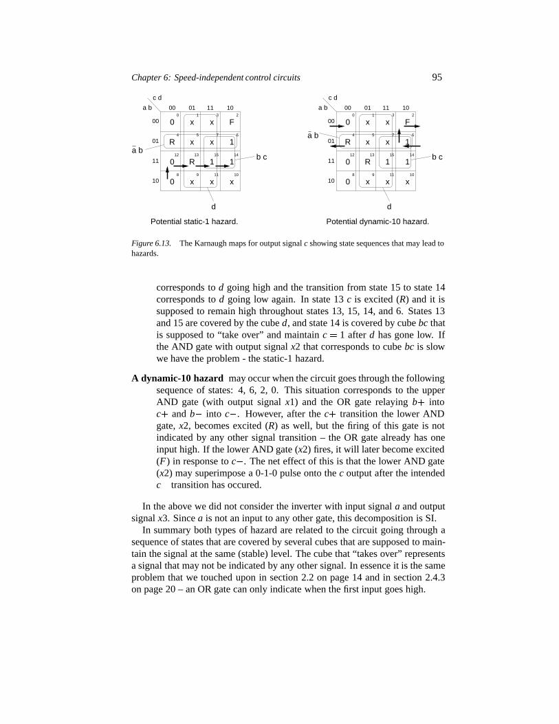
Chapter 6: Speed-independent control circuits 95
Potential dynamic-10 hazard.Potential static-1 hazard.
2
6
14
10
3
7
15
118 9
12 13
54
0 1
10
11
01
10110100
00
c d
a b
0
0 x x x
x x
x x 1
0 1 1
R
R
F
a b
2
6
14
10
3
7
15
118 9
12 13
54
0 1
10
11
01
10110100
00
c d
a b
0
0 x x x
x x
x x 1
0 1 1
R
R
F
a b
d
b c
d
b c
Figure 6.13. The Karnaugh maps for output signalc showing state sequences that may lead tohazards.
corresponds tod going high and the transition from state 15 to state 14corresponds tod going low again. In state 13c is excited (R) and it issupposed to remain high throughout states 13, 15, 14, and 6. States 13and 15 are covered by the cubed, and state 14 is covered by cubebc thatis supposed to “take over” and maintainc � 1 afterd has gone low. Ifthe AND gate with output signalx2 that corresponds to cubebc is slowwe have the problem - the static-1 hazard.
A dynamic-10 hazard may occur when the circuit goes through the followingsequence of states: 4, 6, 2, 0. This situation corresponds to the upperAND gate (with output signalx1) and the OR gate relayingb� intoc� andb� into c�. However, after thec� transition the lower ANDgate,x2, becomes excited (R) as well, but the firing of this gate is notindicated by any other signal transition – the OR gate already has oneinput high. If the lower AND gate (x2) fires, it will later become excited(F) in response toc�. The net effect of this is that the lower AND gate(x2) may superimpose a 0-1-0 pulse onto thec output after the intendedc� transition has occured.
In the above we did not consider the inverter with input signala and outputsignalx3. Sincea is not an input to any other gate, this decomposition is SI.
In summary both types of hazard are related to the circuit going through asequence of states that are covered by several cubes that are supposed to main-tain the signal at the same (stable) level. The cube that “takes over” representsa signal that may not be indicated by any other signal. In essence it is the sameproblem that we touched upon in section 2.2 on page 14 and in section 2.4.3on page 20 – an OR gate can only indicate when the first input goes high.
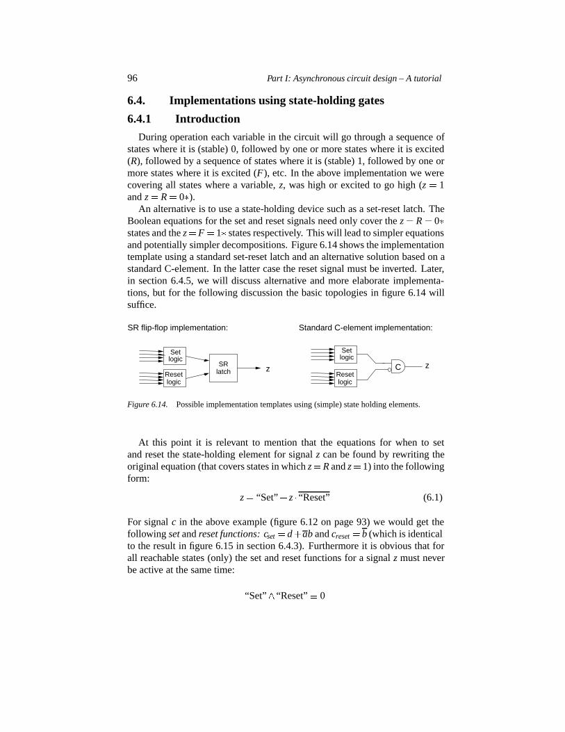
96 Part I: Asynchronous circuit design – A tutorial
6.4. Implementations using state-holding gates
6.4.1 Introduction
During operation each variable in the circuit will go through a sequence ofstates where it is (stable) 0, followed by one or more states where it is excited(R), followed by a sequence of states where it is (stable) 1, followed by one ormore states where it is excited (F), etc. In the above implementation we werecovering all states where a variable,z, was high or excited to go high (z � 1andz � R � 0�).
An alternative is to use a state-holding device such as a set-reset latch. TheBoolean equations for the set and reset signals need only cover thez � R � 0�states and thez�F �1� states respectively. This will lead to simpler equationsand potentially simpler decompositions. Figure 6.14 shows the implementationtemplate using a standard set-reset latch and an alternative solution based on astandard C-element. In the latter case the reset signal must be inverted. Later,in section 6.4.5, we will discuss alternative and more elaborate implementa-tions, but for the following discussion the basic topologies in figure 6.14 willsuffice.
logic
Setlogic
ResetzCz
SR
Resetlogic
Setlogic
latch
Standard C-element implementation:SR flip-flop implementation:
Figure 6.14. Possible implementation templates using (simple) state holding elements.
At this point it is relevant to mention that the equations for when to setand reset the state-holding element for signalz can be found by rewriting theoriginal equation (that covers states in whichz�R andz�1) into the followingform:
z � “Set”� z � “Reset” (6.1)
For signalc in the above example (figure 6.12 on page 93) we would get thefollowing set andreset functions: cset � d�ab andcreset � b (which is identicalto the result in figure 6.15 in section 6.4.3). Furthermore it is obvious that forall reachable states (only) the set and reset functions for a signalz must neverbe active at the same time:
“Set”� “Reset”� 0
Chapter 6: Speed-independent control circuits 97
The following sections will develop the idea of using state-holding elementsand we will illustrate the techniques by re-implementing example 2 from theprevious section.
6.4.2 Excitation regions and quiescent regions
The above idea of using a state-holding device for each variable can be formal-ized as follows:
An excitation region, ER, for a variablez is a maximally-connected set ofstates in which the variable is excited:
ER(z�) denotes a region of states wherez � R � 0*
ER(z�) denotes a region of states wherez � F � 1*
A quiescent region, QR, for a variablez is a maximally-connected set of statesin which the variable is not excited:
QR(z�) denotes a region of states wherez � 1
QR(z�) denotes a region of states wherez � 0
For a given circuit the state space can be disjointly divided into one or moreregions of each type.
Theset function (cover) for a variablez:
must contain all states in the ER(z�) regions
may contain states from the QR(z�) regions
may contain states not reachable by the circuit
Thereset function (cover) for a variablez:
must contain all states in the ER(z�) regions
may contain states from the QR(z�) regions
may contain states not reachable by the circuit
In section 6.4.4 below we will add what is known as themonotonic coverconstraint or theunique entry constraint in order to avoid hazards:
A cube (product term) in the set or reset function of a variable must onlybe entered through a state where the variable is excited.
Having mentioned this last constraint, we have above a complete recipefor the design of speed-independent circuits where each non-input signal isimplemented by a state holding device. Let us continue with example 2.
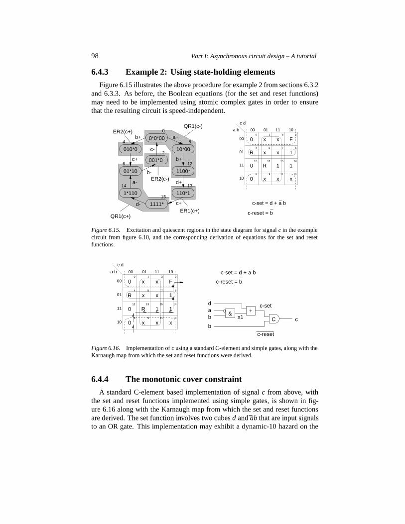
98 Part I: Asynchronous circuit design – A tutorial
6.4.3 Example 2: Using state-holding elements
Figure 6.15 illustrates the above procedure for example 2 from sections 6.3.2and 6.3.3. As before, the Boolean equations (for the set and reset functions)may need to be implemented using atomic complex gates in order to ensurethat the resulting circuit is speed-independent.
ER2(c-)
QR1(c+)
QR1(c-)
ER1(c+)
ER2(c+)a+
b+
d+
c+d-
c-
b-
b+
c+
a-
001*0
10*00
1100*
110*1
1111*
0*0*00
1*110
01*10
010*0
14
6
4
0
8
12
2
15
13
2
6
14
10
3
7
15
118 9
12 13
54
0 1
10
11
01
10110100
00
c d
a b
0
0 x x x
x x
x x 1
0 1 1
R
R
F
c-reset = b
c-set = d + a b
Figure 6.15. Excitation and quiescent regions in the state diagram for signalc in the examplecircuit from figure 6.10, and the corresponding derivation of equations for the set and resetfunctions.
Cx1
c-set
c-reset
2
6
14
10
3
7
15
118 9
12 13
54
0 1
10
11
01
10110100
00
c d
a b
0
0 x x x
x x
x x 1
0 1 1
R
R
F c-reset = b
c-set = d + a b
& +ad
b
bc
Figure 6.16. Implementation ofc using a standard C-element and simple gates, along with theKarnaugh map from which the set and reset functions were derived.
6.4.4 The monotonic cover constraint
A standard C-element based implementation of signalc from above, withthe set and reset functions implemented using simple gates, is shown in fig-ure 6.16 along with the Karnaugh map from which the set and reset functionsare derived. The set function involves two cubesd andab that are input signalsto an OR gate. This implementation may exhibit a dynamic-10 hazard on the
Chapter 6: Speed-independent control circuits 99
cset -signal in a similar way to that discussed previously. The Karnaugh map infigure 6.16 shows the sequence of states that may lead to a malfunction: (8, 12,13, 15, 14, 6, 0). Signald is low in state 12, high in states 13 and 15, and lowagain in state 14. This sequence of states corresponds to a pulse ond. Throughthe OR gate this will create a pulse on thecset signal that will causec to gohigh. Later in state 2,c will go low again. This is the desired behaviour. Theproblem is that the internal signalx1 that corresponds to the other cube in theexpression forcset becomes excited (x1 � R) in state 6. If this AND gate isslow this may produce an unintended pulse on thecset signal afterc has beenreset again.
If the cubeab (that covers states 4, 5, 7, and 6) is reduced to include onlystates 4 and 5 corresponding tocset � d � abc we would avoid the problem.The effect of this modification is that the OR gate is never exposed to morethan one input signal being high, and when this is the case we do not haveproblems with the principle of indication (c.f. the discussion of indication anddual-rail circuits in chapter 2). Another way of expressing this is that a covercube must only be entered through states belonging to an excitation region.This requirement is known as:
the monotonic cover constraint: only one product term in a sum-of-products implementation is allowed to be high at any given time. Obvi-ously the requirement need only be satisfied in the states that are reach-able by the circuit, or alternatively
theunique entry constraint: cover cubes may only be entered throughexcitation region states.
6.4.5 Circuit topologies using state-holding elements
In addition to the set-reset flip-flop and the standard C-element based tem-plates presented above, there are a number of alternative solutions for imple-menting variables using a state-holding device.
A popular approach is thegeneralized C-element that is available to theCMOS transistor-level designer. Here the state-holding mechanism and the setand reset functions are implemented in one (atomic) compound structure ofn- and p-type transistors. Figure 6.17 shows a gate-level symbol for a circuitwherezset � ab andzreset � bc along with dynamic and static CMOS imple-mentations.
An alternative implementation that may be attractive to a designer using astandard cell library that includes (complex) And-Or-Invert gates is shown infigure 6.18. The circuit has the interesting property that it produces both thedesired signalz and its complementz and during transitions itnever produces�z�z� � �1�1�. Again, the example is a circuit wherezset � ab andzreset � bc.
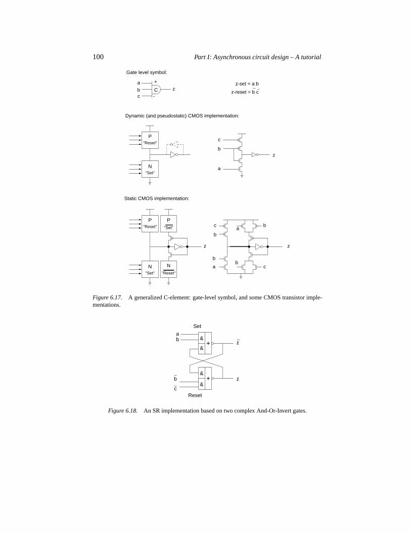
100 Part I: Asynchronous circuit design – A tutorial
P
N"Set"
"Reset"
P"Reset"
N"Set" "Reset"
"Set"
N
P
zz
z-set = a b
z-reset = b c
Dynamic (and pseudostatic) CMOS implementation:
Gate level symbol:
Static CMOS implementation:
+
-
a
bc
zC
b
c b
c
a
bb
a
a
b
c
z
Figure 6.17. A generalized C-element: gate-level symbol, and some CMOS transistor imple-mentations.
&
&
&
&
+
+
Set
Reset
z
z
ab
b
c
Figure 6.18. An SR implementation based on two complex And-Or-Invert gates.
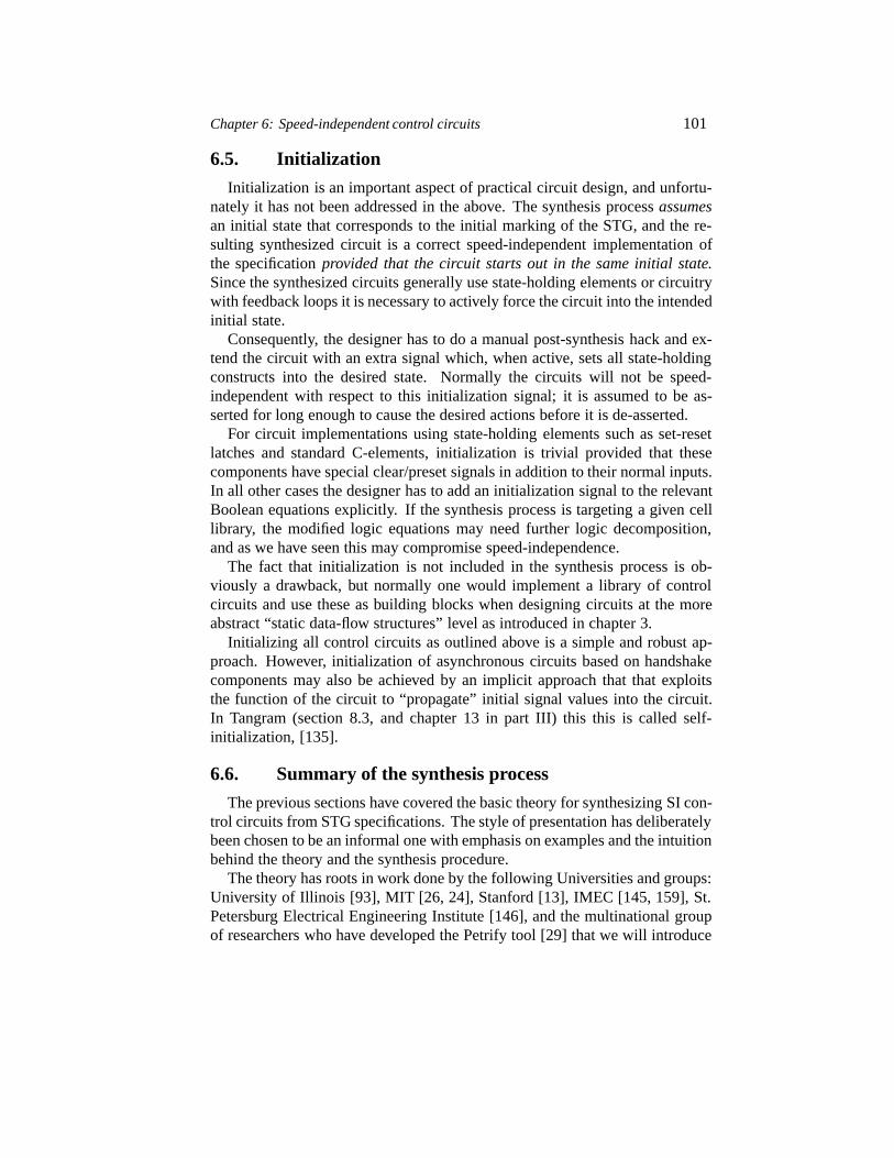
Chapter 6: Speed-independent control circuits 101
6.5. Initialization
Initialization is an important aspect of practical circuit design, and unfortu-nately it has not been addressed in the above. The synthesis processassumesan initial state that corresponds to the initial marking of the STG, and the re-sulting synthesized circuit is a correct speed-independent implementation ofthe specificationprovided that the circuit starts out in the same initial state.Since the synthesized circuits generally use state-holding elements or circuitrywith feedback loops it is necessary to actively force the circuit into the intendedinitial state.
Consequently, the designer has to do a manual post-synthesis hack and ex-tend the circuit with an extra signal which, when active, sets all state-holdingconstructs into the desired state. Normally the circuits will not be speed-independent with respect to this initialization signal; it is assumed to be as-serted for long enough to cause the desired actions before it is de-asserted.
For circuit implementations using state-holding elements such as set-resetlatches and standard C-elements, initialization is trivial provided that thesecomponents have special clear/preset signals in addition to their normal inputs.In all other cases the designer has to add an initialization signal to the relevantBoolean equations explicitly. If the synthesis process is targeting a given celllibrary, the modified logic equations may need further logic decomposition,and as we have seen this may compromise speed-independence.
The fact that initialization is not included in the synthesis process is ob-viously a drawback, but normally one would implement a library of controlcircuits and use these as building blocks when designing circuits at the moreabstract “static data-flow structures” level as introduced in chapter 3.
Initializing all control circuits as outlined above is a simple and robust ap-proach. However, initialization of asynchronous circuits based on handshakecomponents may also be achieved by an implicit approach that that exploitsthe function of the circuit to “propagate” initial signal values into the circuit.In Tangram (section 8.3, and chapter 13 in part III) this this is called self-initialization, [135].
6.6. Summary of the synthesis process
The previous sections have covered the basic theory for synthesizing SI con-trol circuits from STG specifications. The style of presentation has deliberatelybeen chosen to be an informal one with emphasis on examples and the intuitionbehind the theory and the synthesis procedure.
The theory has roots in work done by the following Universities and groups:University of Illinois [93], MIT [26, 24], Stanford [13], IMEC [145, 159], St.Petersburg Electrical Engineering Institute [146], and the multinational groupof researchers who have developed the Petrify tool [29] that we will introduce
102 Part I: Asynchronous circuit design – A tutorial
in the next section. This author has attended several discussions from whichit is clear that in some cases the concepts and theories have been developedindependently by several groups, and I will refrain from attempting a precisehistory of the evolution. The reader who is interested in digging deeper into thesubject is encouraged to consult the literature; in particular the book by Myers[95].
In summary the synthesis process outlined in the previous sections involvesthe following steps:
1 Specify the desired behaviour of the circuit and its (dummy) environ-ment using an STG.
2 Check that the STG satisfies properties 1-5 on page 88: 1-bounded, con-sistent state assignment, liveness, only input free choice and controlledchoice and persistency. An STG satisfying these conditions is a validspecification of an SI circuit.
3 Check that the specification satisfies property 6 on page 88: completestate coding (CSC). If the specification does not satisfy CSC it is neces-sary to add one or more state variables or to change the specification(which is often possible in 4-phase control circuits where the down-going signal transitions can be shuffled around). Some tools (includingPetrify) can insert state variables automatically, whereas re-shuffling ofsignals – which represents a modification of the specification – is a taskfor the designer.
4 Select an implementation template and derive the Boolean equations forthe variables themselves, or for the set and reset functions when stateholding devices are used. Also decide if these equations can be imple-mented in atomic gates (typically complex AOI-gates) or if they are tobe implemented by structures of simpler gates. These decisions may beset by switches in the synthesis tools.
5 Derive the Boolean equations for the desired implementation template.
6 Manually modify the implementation such that the circuit can be forcedinto the desired initial state by an explicit reset or initialization signal.
7 Enter the design into a CAD tool and perform simulation and layout ofthe circuit (or the system in which the circuit is used as a component).
6.7. Petrify: A tool for synthesizing SI circuits from STGs
Petrify is a public domain tool for manipulating Petri nets and for syn-thesizing SI control circuits from STG specifications. It is available fromhttp://www.lsi.upc.es/˜jordic/petrify/petrify.html.
Chapter 6: Speed-independent control circuits 103
Petrify is a typical UNIX program with many options and switches. As acircuit designer one would probably prefer a push-button synthesis tool thataccepts a specification and produces a circuit. Petrify can be used this way butit is more than this. If you know how to play the game it is an interactive toolfor specifying, checking, and manipulating Petri nets, STGs and state graphs.In the following section we will show some examples of how to design speed-independent control circuits.
Input to Petrify is an STG described in a simple textual format. Using theprogram drawastg that is part of the Petrify distribution (and that is basedon the graph visualization package ‘dot’ developed at AT&T) it is possible toproduce a drawing of the STGs and state graphs. The graphs are “nice” but thetopological organization may be very different from how the designer thinksabout the problem. Even the simple task of checking that an STG entered intextual form is indeed the intended STG may be difficult.
To help ease this situation a graphical STG entry and simulation tool calledVSTGL (Visual STG Lab) has been developed at the Technical University ofDenmark. To help the designer obtain a correct specification VSTGL includesan interactive simulator that allows the designer to add tokens and to fire tran-sitions. It also carries out certain simple checks on the STG.
VSTGL is available fromhttp://vstgl.sourceforge.net/ and it is theresult of a small student project done by two 4th year students. VSTGL is sta-ble and reliable, though naming of signal transitions may seem a bit awkward.
Petrify can solve CSC violations by inserting state variables, and it can becontrolled to target the implementation templates introduced in section 6.4:
The-cgoption will produce a complex-gate circuit (one where each non-input signal is implemented in a single complex gate).
The-gcoption will produce a generalized C-element circuit. The outputsfrom Petrify are the Boolean equations for the set and reset functions foreach non-input signal.
The -gcm option will produce a generalized C-element solution wherethe set and reset functions satisfy the monotonic cover requirement. Con-sequently the solution can also be mapped onto a standard C-elementimplementation where theset andreset functions are implemented us-ing simple AND and OR gates.
The -tm option will cause Petrify to perform technology mapping ontoa gate library that can be specified by the user. Technology mapping canobviously not be combined with the-cg and-gc options.
Petrify comes with a manual and some examples. In the following sectionwe will go through some examples drawn from the previous chapters of thebook.
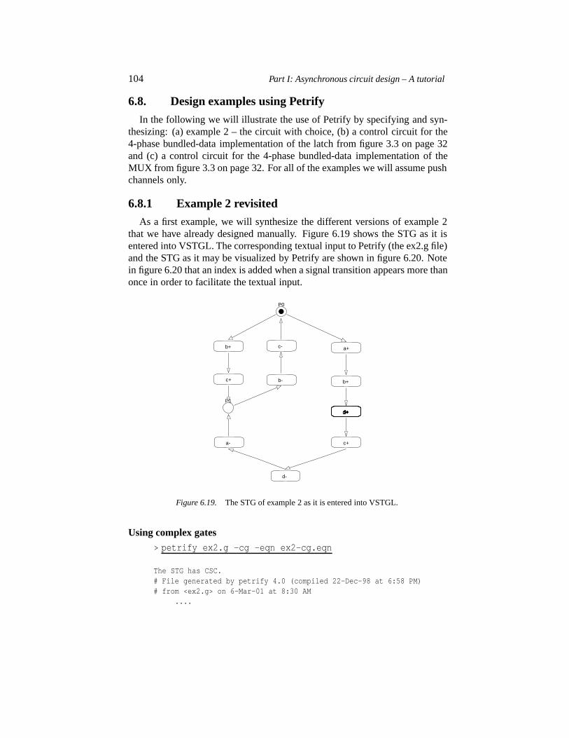
104 Part I: Asynchronous circuit design – A tutorial
6.8. Design examples using Petrify
In the following we will illustrate the use of Petrify by specifying and syn-thesizing: (a) example 2 – the circuit with choice, (b) a control circuit for the4-phase bundled-data implementation of the latch from figure 3.3 on page 32and (c) a control circuit for the 4-phase bundled-data implementation of theMUX from figure 3.3 on page 32. For all of the examples we will assume pushchannels only.
6.8.1 Example 2 revisited
As a first example, we will synthesize the different versions of example 2that we have already designed manually. Figure 6.19 shows the STG as it isentered into VSTGL. The corresponding textual input to Petrify (the ex2.g file)and the STG as it may be visualized by Petrify are shown in figure 6.20. Notein figure 6.20 that an index is added when a signal transition appears more thanonce in order to facilitate the textual input.
P0
c+
b+
P1
c-
b-
a-
d-
c+
a+
b+
d+d+d+d+d+d+d+d+
Figure 6.19. The STG of example 2 as it is entered into VSTGL.
Using complex gates
> petrify ex2.g -cg -eqn ex2-cg.eqn
The STG has CSC.# File generated by petrify 4.0 (compiled 22-Dec-98 at 6:58 PM)# from <ex2.g> on 6-Mar-01 at 8:30 AM
....
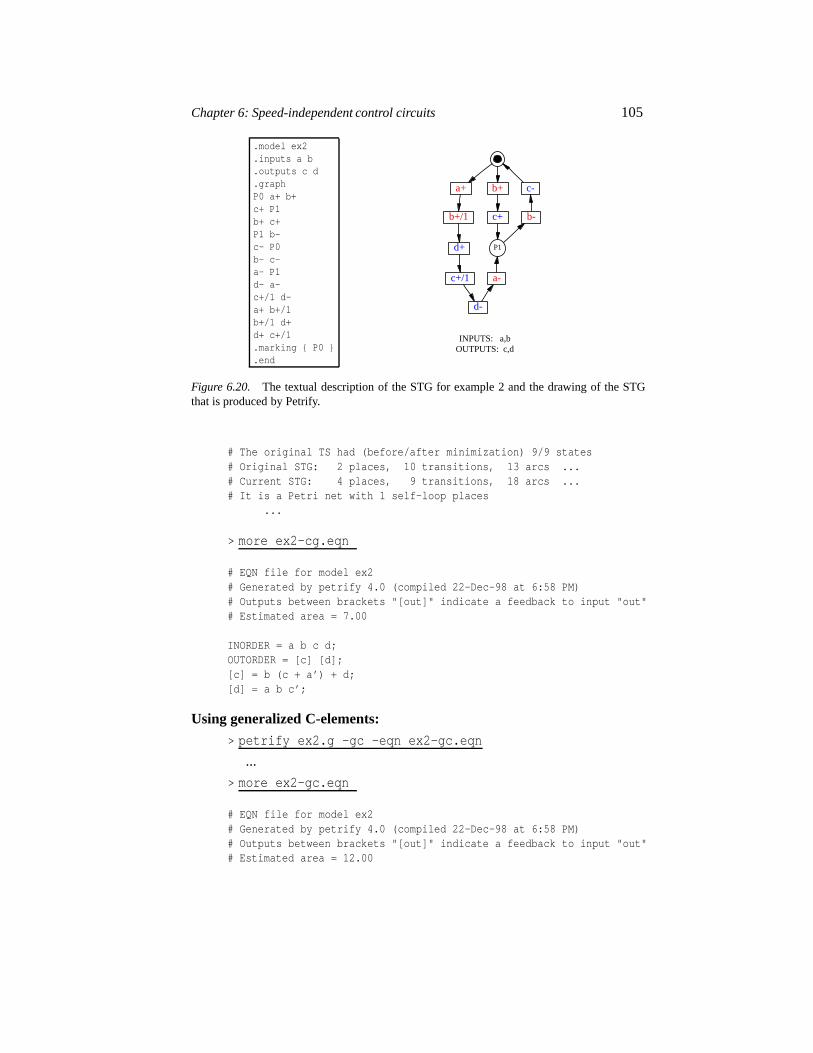
Chapter 6: Speed-independent control circuits 105
.model ex2
.inputs a b
.outputs c d
.graphP0 a+ b+c+ P1b+ c+P1 b-c- P0b- c-a- P1d- a-c+/1 d-a+ b+/1b+/1 d+d+ c+/1.marking { P0 }.end
INPUTS: a,bOUTPUTS: c,d
P0
a+ b+
b+/1 c+
c-
P1
b-
d+
c+/1 a-
d-
Figure 6.20. The textual description of the STG for example 2 and the drawing of the STGthat is produced by Petrify.
# The original TS had (before/after minimization) 9/9 states# Original STG: 2 places, 10 transitions, 13 arcs ...# Current STG: 4 places, 9 transitions, 18 arcs ...# It is a Petri net with 1 self-loop places
...
> more ex2-cg.eqn
# EQN file for model ex2# Generated by petrify 4.0 (compiled 22-Dec-98 at 6:58 PM)# Outputs between brackets "[out]" indicate a feedback to input "out"# Estimated area = 7.00
INORDER = a b c d;OUTORDER = [c] [d];[c] = b (c + a’) + d;[d] = a b c’;
Using generalized C-elements:
> petrify ex2.g -gc -eqn ex2-gc.eqn
...
> more ex2-gc.eqn
# EQN file for model ex2# Generated by petrify 4.0 (compiled 22-Dec-98 at 6:58 PM)# Outputs between brackets "[out]" indicate a feedback to input "out"# Estimated area = 12.00
106 Part I: Asynchronous circuit design – A tutorial
INORDER = a b c d;OUTORDER = [c] [d];[0] = a’ b + d;[1] = a b c’;[d] = d c’ + [1]; # mappable onto gC[c] = c b + [0]; # mappable onto gC
The equations for the generalized C-elements should be “interpreted”according to equation 6.1 on page 96
Using standard C-elementsand set/reset functions that satisfy themonotoniccover constraint:
> petrify ex2.g -gcm -eqn ex2-gcm.eqn
...
> more ex2-gcm.eqn
# EQN file for model ex2# Generated by petrify 4.0 (compiled 22-Dec-98 at 6:58 PM)# Outputs between brackets "[out]" indicate a feedback to input "out"# Estimated area = 10.00
INORDER = a b c d;OUTORDER = [c] [d];[0] = a’ b c’ + d;[d] = a b c’;[c] = c b + [0]; # mappable onto gC
Again, the equations for the generalized C-element should be “interpreted”according to equation 6.1 on page 96.
6.8.2 Control circuit for a 4-phase bundled-data latch
Figure 6.21 shows an asynchronous handshake latch with a dummy environ-ment on its left and right side. The latch can be implemented using a normalN-bit wide transparent latch and the control circuit we are about to design.A driver may be needed for the latch control signalLt. In order to make thelatch controller robust and independent of the delay in this driver, we may feedthe buffered signal (Lt) back such that the controller knows when the signalhas been presented to the latch. Figure 6.21 also shows fragments of the STGspecification – the handshaking of the left and right hand environments andideas about the behaviour of the latch controller. InitiallyLt is low and thelatch is transparent, and when new input data arrives they will flow throughthe latch. In response toRin�, and provided that the right hand environmentis ready for another handshake (Aout � 0), the controller may generateRout�
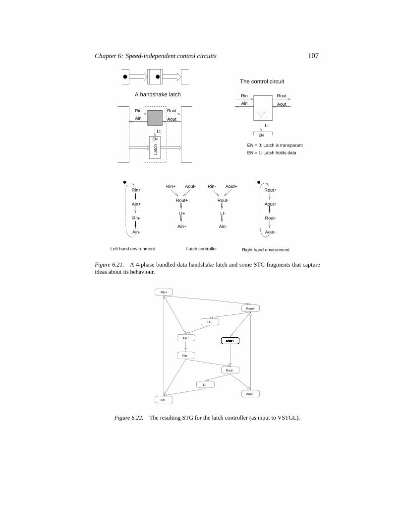
Chapter 6: Speed-independent control circuits 107
Latch controller Right hand environment
Lt-Lt+
Rin+
Ain+
Rin-
Ain-
Rin+ Aout-
Rout+
Ain+
Rin- Aout+
Rout-
Ain-
Rout+
Aout+
Rout-
Aout-
Left hand environment
ENEN
EN = 0: Latch is transparant
EN = 1: Latch holds data
The control circuit
A handshake latch
Latc
h
Lt
Rin
Ain
Rout
Aout
Lt
Rin
Ain
Rout
Aout
Figure 6.21. A 4-phase bundled-data handshake latch and some STG fragments that captureideas about its behaviour.
Rout+
Rin+
Lt+
Ain+
Rin-
Rout-
Lt-
Ain-
Aout-
Aout+Aout+Aout+Aout+Aout+Aout+Aout+Aout+Aout+Aout+Aout+Aout+Aout+Aout+Aout+
Figure 6.22. The resulting STG for the latch controller (as input to VSTGL).
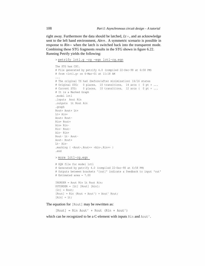
108 Part I: Asynchronous circuit design – A tutorial
right away. Furthermore the data should be latched,Lt�, and an acknowledgesent to the left hand environment,Ain�. A symmetric scenario is possible inresponse toRin� when the latch is switched back into the transparent mode.Combining these STG fragments results in the STG shown in figure 6.22.Running Petrify yields the following:
> petrify lctl.g -cg -eqn lctl-cg.eqn
The STG has CSC.# File generated by petrify 4.0 (compiled 22-Dec-98 at 6:58 PM)# from <lctl.g> on 6-Mar-01 at 11:18 AM...# The original TS had (before/after minimization) 16/16 states# Original STG: 0 places, 10 transitions, 14 arcs ( 0 pt + ...# Current STG: 0 places, 10 transitions, 12 arcs ( 0 pt + ...# It is a Marked Graph.model lctl.inputs Aout Rin.outputs Lt Rout Ain.graphRout+ Aout+ Lt+Lt+ Ain+Aout+ Rout-Rin+ Rout+Ain+ Rin-Rin- Rout-Ain- Rin+Rout- Lt- Aout-Aout- Rout+Lt- Ain-.marking { <Aout-,Rout+> <Ain-,Rin+> }.end
> more lctl-cg.eqn
# EQN file for model lctl# Generated by petrify 4.0 (compiled 22-Dec-98 at 6:58 PM)# Outputs between brackets "[out]" indicate a feedback to input "out"# Estimated area = 7.00
INORDER = Aout Rin Lt Rout Ain;OUTORDER = [Lt] [Rout] [Ain];[Lt] = Rout;[Rout] = Rin (Rout + Aout’) + Aout’ Rout;[Ain] = Lt;
The equation for[Rout] may be rewritten as:
[Rout] = Rin Aout’ + Rout (Rin + Aout’)
which can be recognized to be a C-element with inputsRin andAout’.
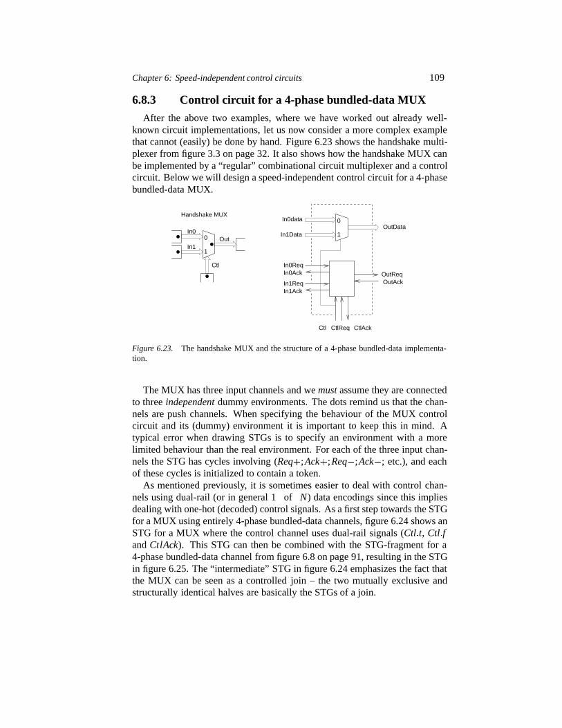
Chapter 6: Speed-independent control circuits 109
6.8.3 Control circuit for a 4-phase bundled-data MUX
After the above two examples, where we have worked out already well-known circuit implementations, let us now consider a more complex examplethat cannot (easily) be done by hand. Figure 6.23 shows the handshake multi-plexer from figure 3.3 on page 32. It also shows how the handshake MUX canbe implemented by a “regular” combinational circuit multiplexer and a controlcircuit. Below we will design a speed-independent control circuit for a 4-phasebundled-data MUX.
CtlReqCtl CtlAck
Handshake MUX
0
1
In0
In1Out
Ctl
0
1
In1ReqIn1Ack
In0AckIn0Req
In1Data
In0data
OutAckOutReq
OutData
Figure 6.23. The handshake MUX and the structure of a 4-phase bundled-data implementa-tion.
The MUX has three input channels and wemust assume they are connectedto threeindependent dummy environments. The dots remind us that the chan-nels are push channels. When specifying the behaviour of the MUX controlcircuit and its (dummy) environment it is important to keep this in mind. Atypical error when drawing STGs is to specify an environment with a morelimited behaviour than the real environment. For each of the three input chan-nels the STG has cycles involving (Req�;Ack�;Req�;Ack�; etc.), and eachof these cycles is initialized to contain a token.
As mentioned previously, it is sometimes easier to deal with control chan-nels using dual-rail (or in general 1�of�N) data encodings since this impliesdealing with one-hot (decoded) control signals. As a first step towards the STGfor a MUX using entirely 4-phase bundled-data channels, figure 6.24 shows anSTG for a MUX where the control channel uses dual-rail signals (Ctl�t, Ctl�fandCtlAck). This STG can then be combined with the STG-fragment for a4-phase bundled-data channel from figure 6.8 on page 91, resulting in the STGin figure 6.25. The “intermediate” STG in figure 6.24 emphasizes the fact thatthe MUX can be seen as a controlled join – the two mutually exclusive andstructurally identical halves are basically the STGs of a join.
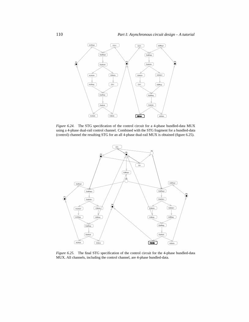
110 Part I: Asynchronous circuit design – A tutorial
Ctl.t+
CtlAck+
OutReq+
OutAck+
In1Ack+
In1Req-
OutReq-
OutAck-
In1Ack-
OutAck+
In0Req+
In0Ack+
In0Req-
OutReq-
OutAck-
In0Ack-
In1Req+ Ctl.f+
CtlAck+
OutReq+
P2P1 P0
Ctl.t- Ctl.f-
CtlAck- CtlAck-CtlAck-CtlAck-CtlAck-CtlAck-CtlAck-CtlAck-CtlAck-CtlAck-CtlAck-CtlAck-CtlAck-CtlAck-CtlAck-CtlAck-CtlAck-CtlAck-CtlAck-CtlAck-CtlAck-CtlAck-CtlAck-CtlAck-CtlAck-CtlAck-
Figure 6.24. The STG specification of the control circuit for a 4-phase bundled-data MUXusing a 4-phase dual-rail control channel. Combined with the STG fragment for a bundled-data(control) channel the resulting STG for an all 4-phase dual-rail MUX is obtained (figure 6.25).
Ctl-
Ctl+
CtlReq+
P5
P2
P3
P4
OutReq+
CtlAck+
CtlAck-
CtlReq-
OutReq+
OutAck+
In1Ack+
In1Req-
OutReq-
OutAck-
In1Ack-
OutAck+
In0Req+
In0Ack+
In0Req-
OutReq-
OutAck-
In0Ack-
In1Req+
P1
P0
P6
CtlReq-
CtlAck+
CtlAck-CtlAck-CtlAck-CtlAck-CtlAck-CtlAck-CtlAck-CtlAck-CtlAck-CtlAck-CtlAck-CtlAck-CtlAck-CtlAck-CtlAck-CtlAck-CtlAck-CtlAck-CtlAck-CtlAck-CtlAck-CtlAck-CtlAck-
Figure 6.25. The final STG specification of the control circuit for the 4-phase bundled-dataMUX. All channels, including the control channel, are 4-phase bundled-data.
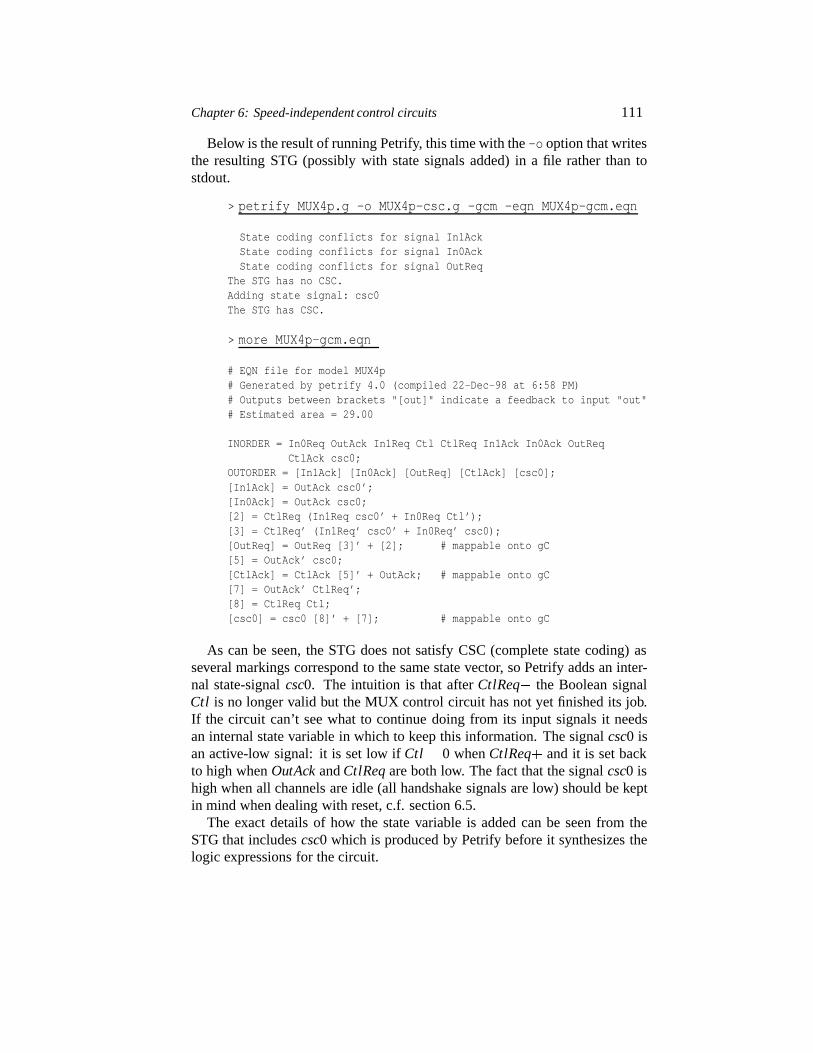
Chapter 6: Speed-independent control circuits 111
Below is the result of running Petrify, this time with the-o option that writesthe resulting STG (possibly with state signals added) in a file rather than tostdout.
> petrify MUX4p.g -o MUX4p-csc.g -gcm -eqn MUX4p-gcm.eqn
State coding conflicts for signal In1AckState coding conflicts for signal In0AckState coding conflicts for signal OutReq
The STG has no CSC.Adding state signal: csc0The STG has CSC.
> more MUX4p-gcm.eqn
# EQN file for model MUX4p# Generated by petrify 4.0 (compiled 22-Dec-98 at 6:58 PM)# Outputs between brackets "[out]" indicate a feedback to input "out"# Estimated area = 29.00
INORDER = In0Req OutAck In1Req Ctl CtlReq In1Ack In0Ack OutReqCtlAck csc0;
OUTORDER = [In1Ack] [In0Ack] [OutReq] [CtlAck] [csc0];[In1Ack] = OutAck csc0’;[In0Ack] = OutAck csc0;[2] = CtlReq (In1Req csc0’ + In0Req Ctl’);[3] = CtlReq’ (In1Req’ csc0’ + In0Req’ csc0);[OutReq] = OutReq [3]’ + [2]; # mappable onto gC[5] = OutAck’ csc0;[CtlAck] = CtlAck [5]’ + OutAck; # mappable onto gC[7] = OutAck’ CtlReq’;[8] = CtlReq Ctl;[csc0] = csc0 [8]’ + [7]; # mappable onto gC
As can be seen, the STG does not satisfy CSC (complete state coding) asseveral markings correspond to the same state vector, so Petrify adds an inter-nal state-signalcsc0. The intuition is that afterCtlReq� the Boolean signalCtl is no longer valid but the MUX control circuit has not yet finished its job.If the circuit can’t see what to continue doing from its input signals it needsan internal state variable in which to keep this information. The signalcsc0 isan active-low signal: it is set low ifCtl � 0 whenCtlReq� and it is set backto high whenOutAck andCtlReq are both low. The fact that the signalcsc0 ishigh when all channels are idle (all handshake signals are low) should be keptin mind when dealing with reset, c.f. section 6.5.
The exact details of how the state variable is added can be seen from theSTG that includescsc0 which is produced by Petrify before it synthesizes thelogic expressions for the circuit.
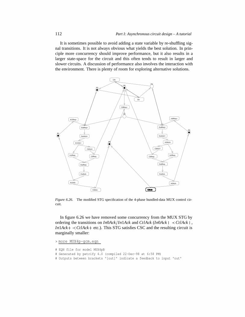
112 Part I: Asynchronous circuit design – A tutorial
It is sometimes possible to avoid adding a state variable by re-shuffling sig-nal transitions. It is not always obvious what yields the best solution. In prin-ciple more concurrency should improve performance, but it also results in alarger state-space for the circuit and this often tends to result in larger andslower circuits. A discussion of performance also involves the interaction withthe environment. There is plenty of room for exploring alternative solutions.
Ctl-
Ctl+
CtlReq+
P5
P2
P3
P4
OutReq+
CtlAck+
CtlAck-
CtlReq-
OutReq+
OutAck+
In1Ack+
In1Req-
OutReq-
OutAck-
In1Ack-
OutAck+
In0Req+
In0Ack+
In0Req-
OutReq-
OutAck-
In0Ack-
In1Req+
P1
P0
P6
CtlReq-
CtlAck+
CtlAck-CtlAck-CtlAck-CtlAck-CtlAck-CtlAck-CtlAck-CtlAck-CtlAck-CtlAck-CtlAck-CtlAck-CtlAck-CtlAck-CtlAck-CtlAck-CtlAck-CtlAck-CtlAck-CtlAck-CtlAck-CtlAck-CtlAck-
Figure 6.26. The modified STG specification of the 4-phase bundled-data MUX control cir-cuit.
In figure 6.26 we have removed some concurrency from the MUX STG byordering the transitions onIn0Ack�In1Ack andCtlAck (In0Ack� �CtlAck�,In1Ack��CtlAck� etc.). This STG satisfies CSC and the resulting circuit ismarginally smaller:
> more MUX4p-gcm.eqn
# EQN file for model MUX4pB# Generated by petrify 4.0 (compiled 22-Dec-98 at 6:58 PM)# Outputs between brackets "[out]" indicate a feedback to input "out"
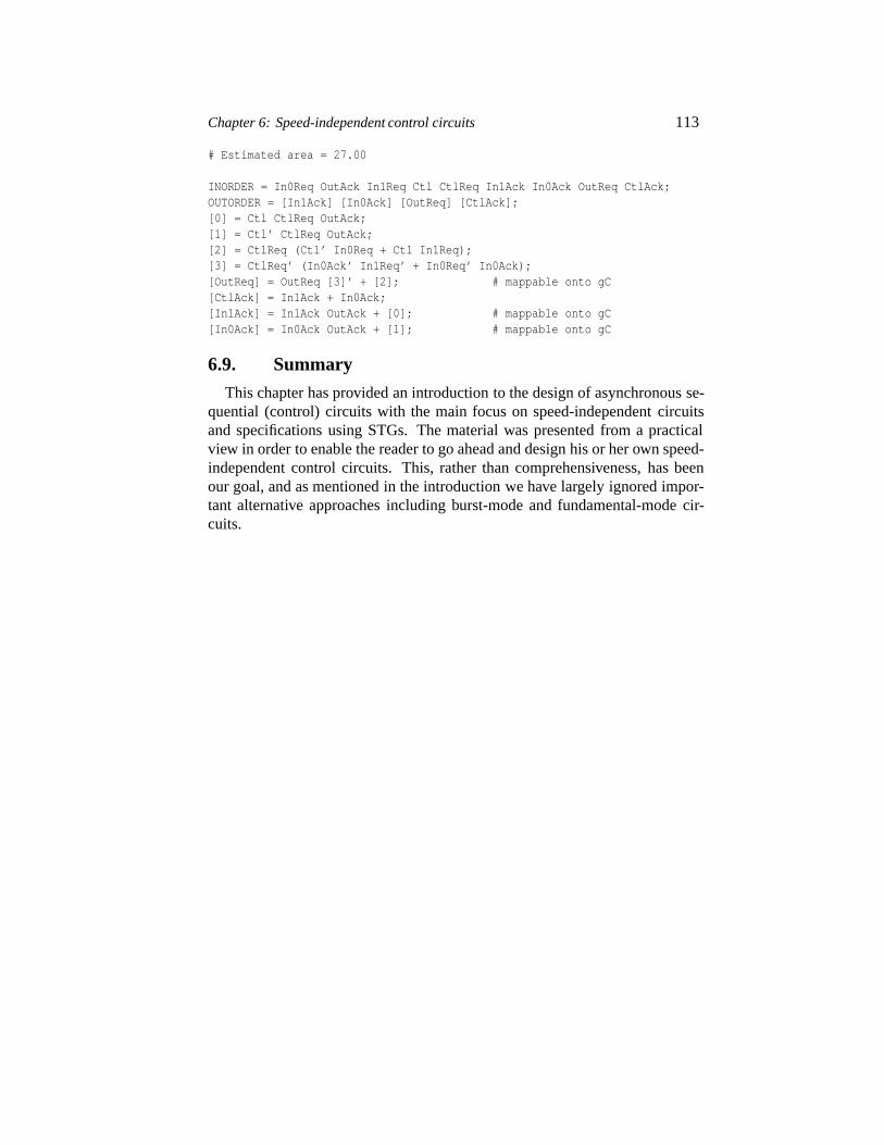
Chapter 6: Speed-independent control circuits 113
# Estimated area = 27.00
INORDER = In0Req OutAck In1Req Ctl CtlReq In1Ack In0Ack OutReq CtlAck;OUTORDER = [In1Ack] [In0Ack] [OutReq] [CtlAck];[0] = Ctl CtlReq OutAck;[1] = Ctl’ CtlReq OutAck;[2] = CtlReq (Ctl’ In0Req + Ctl In1Req);[3] = CtlReq’ (In0Ack’ In1Req’ + In0Req’ In0Ack);[OutReq] = OutReq [3]’ + [2]; # mappable onto gC[CtlAck] = In1Ack + In0Ack;[In1Ack] = In1Ack OutAck + [0]; # mappable onto gC[In0Ack] = In0Ack OutAck + [1]; # mappable onto gC
6.9. Summary
This chapter has provided an introduction to the design of asynchronous se-quential (control) circuits with the main focus on speed-independent circuitsand specifications using STGs. The material was presented from a practicalview in order to enable the reader to go ahead and design his or her own speed-independent control circuits. This, rather than comprehensiveness, has beenour goal, and as mentioned in the introduction we have largely ignored impor-tant alternative approaches including burst-mode and fundamental-mode cir-cuits.

Chapter 7
ADVANCED 4-PHASE BUNDLED-DATAPROTOCOLS AND CIRCUITS
The previous chapters have explained the basics of asynchronous circuitdesign. In this chapter we will address 4-phase bundled-data protocols andcircuits in more detail. This will include: (1) a variety of channel types, (2)protocols with different data-validity schemes, and (3) a number of more so-phisticated latch control circuits. These latch controllers are interesting fortwo reasons: they are very useful in optimizing the circuits for area, power andspeed, and they are nice examples of the types of control circuits that can bespecified and synthesized using the STG-based techniques from the previouschapter.
7.1. Channels and protocols
7.1.1 Channel types
So far we have considered onlypush channels where the sender is the activeparty that initiates the communication of data, and where the receiver is thepassive party. The opposite situation, where the receiver is the active partythat initiates the communication of data, is also possible, and such a channelis called apull channel. A channel that carries no data is called anonputchannel and is used for synchronization purposes. Finally, it is also possibleto communicate data from a receiver to a sender along with the acknowledgesignal. Such a channel is called abiput channel. In a 4-phase bundled-dataimplementation data from the receiver is bundled with the acknowledge, and ina 4-phase dual-rail protocol the passive party will acknowledge the receptionof a codeword by returning a codeword rather than just an an acknowledgesignal. Figure 7.1 illustrates these four channel types (nonput, push, pull, andbiput) assuming a bundled-data protocol. Each channel type may, of course,use any of the handshake protocols (2-phase or 4-phase) and data encodings(bundled-data, dual-rail,m�of�n, etc.) introduced previously.
115
116 Part I: Asynchronous circuit design – A tutorial
7.1.2 Data-validity schemes
For the bundled-data protocols it is also relevant to define the time intervalin which data is valid, and figure 7.2 illustrates the different possibilities.
For a push channel the request signal carries the message “here is new datafor you” and the acknowledge signal carries the information “thank you, I haveabsorbed the data, and you may release the data wires.” Similarly, for a pullchannel the request signal carries the message “please send new data” and theacknowledge signal carries the message “here is the data that you requested.”It is the signal transitions on the request and acknowledge wires that are in-terpreted in this way. A 4-phase handshake involves two transitions on eachwire and, depending on whether it is the rising or the falling transitions onthe request and acknowledge signals that are interpreted in this way, severaldata-validity schemes emerge: early, broad, late and extended early.
Since 2-phase handshaking does not involve any redundant signal transitionsthere is only one data-validity scheme for each channel type (push or pull), asillustrated in figure 7.2.
It is common to all of the data-validity schemes that the data is valid sometime before the event that indicates the start of the interval, and that it remainsstable until some time after the event that indicates the end of the interval.Furthermore, all of the data-validity schemes express the requirements of theparty that receives the data. The fact that a receiver signals “thank you, I haveabsorbed the data, and you may go ahead and release the data wires,” doesnot mean that this actually happens – the sender may prolong the data-validityinterval, and the receiver may even rely on this.
A typical example of this is the extended-early data-validity schemes in fig-ure 7.2. On a push channel the data-validity interval begins some time beforeReq and ends some time afterReq .
7.1.3 Discussion
The above classification of channel types and handshake protocols stemsmostly from Peeters’ Ph.D. thesis [112]. The choice of channel type, hand-shake protocol and data-validity scheme obviously affects the implementationof the handshake components in terms of area, speed, and power. Just as adesign may use a mix of different bundled-data and dual-rail protocols, it mayalso use a mix of channel types and data-validity schemes.
For example, a 4-phase bundled-data push channel using a broad or anextended-early data-validity scheme is a very convenient input to a functionblock that is implemented using precharged CMOS circuitry: the request signalmay directly control the precharge and evaluate transistors because the broadand the extended-early data-validity schemes guarantee that the input data isstable during the evaluate phase.
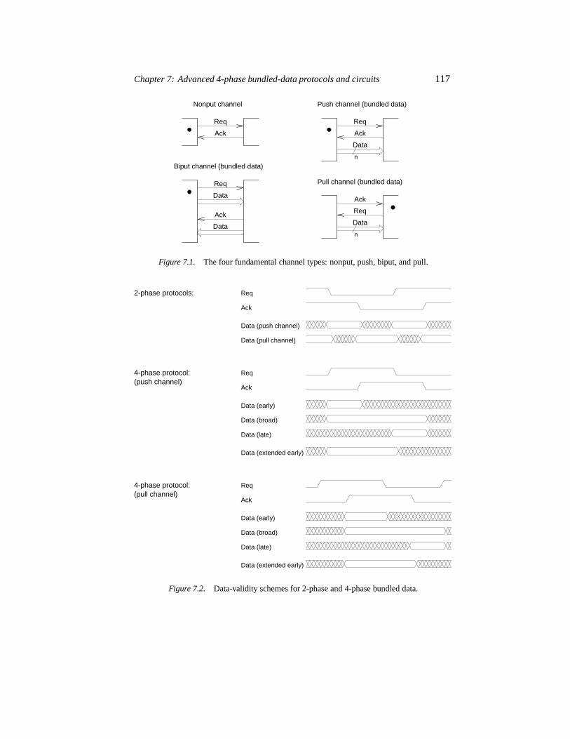
Chapter 7: Advanced 4-phase bundled-data protocols and circuits 117
n
Data
Ack
Req
n
Ack
Req
Req
Data
Data
Ack
Nonput channel
Data
Ack
Req
Biput channel (bundled data)
Push channel (bundled data)
Pull channel (bundled data)
Figure 7.1. The four fundamental channel types: nonput, push, biput, and pull.
Data (early)
4-phase protocol:(push channel)
Ack
Req
Data (broad)
Data (late)
Data (extended early)
Data (early)
Ack
Req
Data (broad)
Data (late)
Data (extended early)
4-phase protocol:(pull channel)
Ack
Req
Data (pull channel)
2-phase protocols:
Data (push channel)
Figure 7.2. Data-validity schemes for 2-phase and 4-phase bundled data.
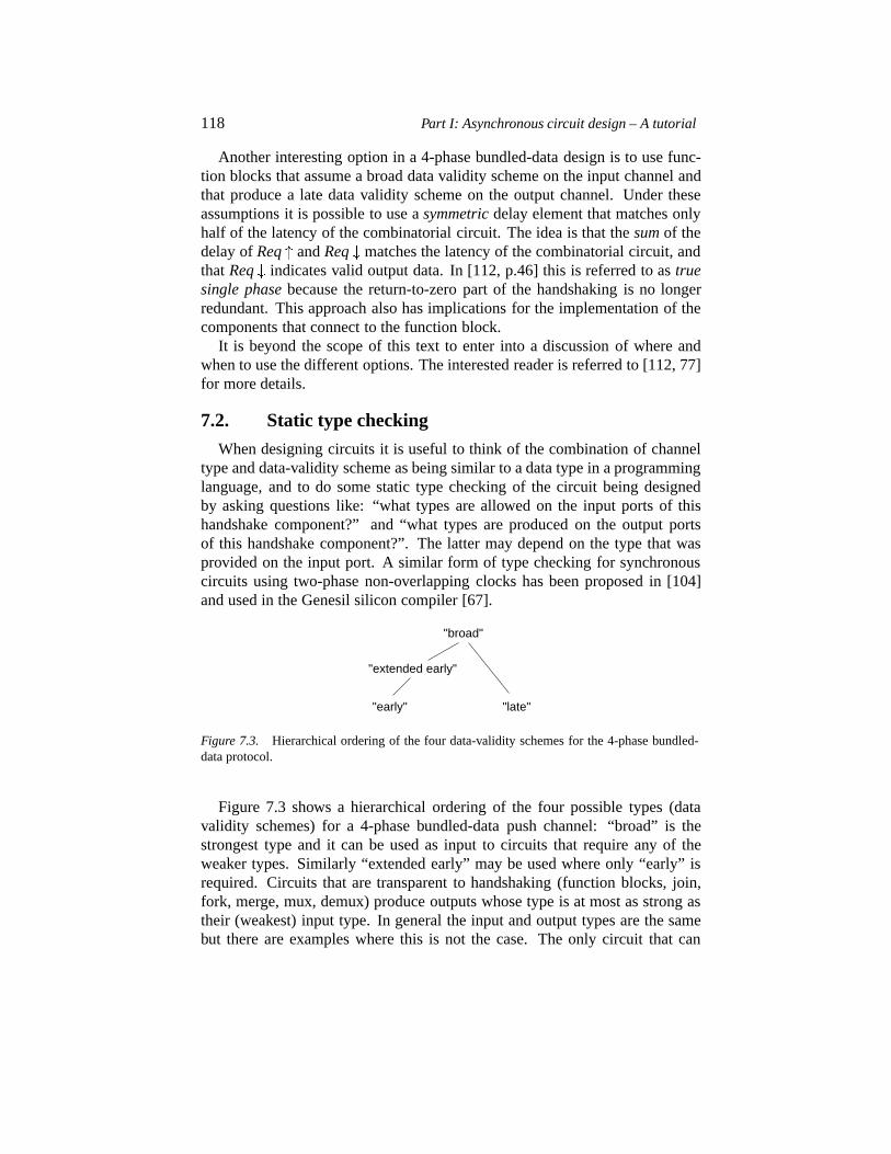
118 Part I: Asynchronous circuit design – A tutorial
Another interesting option in a 4-phase bundled-data design is to use func-tion blocks that assume a broad data validity scheme on the input channel andthat produce a late data validity scheme on the output channel. Under theseassumptions it is possible to use asymmetric delay element that matches onlyhalf of the latency of the combinatorial circuit. The idea is that thesum of thedelay ofReq andReq matches the latency of the combinatorial circuit, andthatReq indicates valid output data. In [112, p.46] this is referred to astruesingle phase because the return-to-zero part of the handshaking is no longerredundant. This approach also has implications for the implementation of thecomponents that connect to the function block.
It is beyond the scope of this text to enter into a discussion of where andwhen to use the different options. The interested reader is referred to [112, 77]for more details.
7.2. Static type checking
When designing circuits it is useful to think of the combination of channeltype and data-validity scheme as being similar to a data type in a programminglanguage, and to do some static type checking of the circuit being designedby asking questions like: “what types are allowed on the input ports of thishandshake component?” and “what types are produced on the output portsof this handshake component?”. The latter may depend on the type that wasprovided on the input port. A similar form of type checking for synchronouscircuits using two-phase non-overlapping clocks has been proposed in [104]and used in the Genesil silicon compiler [67].
"broad"
"extended early"
"late""early"
Figure 7.3. Hierarchical ordering of the four data-validity schemes for the 4-phase bundled-data protocol.
Figure 7.3 shows a hierarchical ordering of the four possible types (datavalidity schemes) for a 4-phase bundled-data push channel: “broad” is thestrongest type and it can be used as input to circuits that require any of theweaker types. Similarly “extended early” may be used where only “early” isrequired. Circuits that are transparent to handshaking (function blocks, join,fork, merge, mux, demux) produce outputs whose type is at most as strong astheir (weakest) input type. In general the input and output types are the samebut there are examples where this is not the case. The only circuit that can
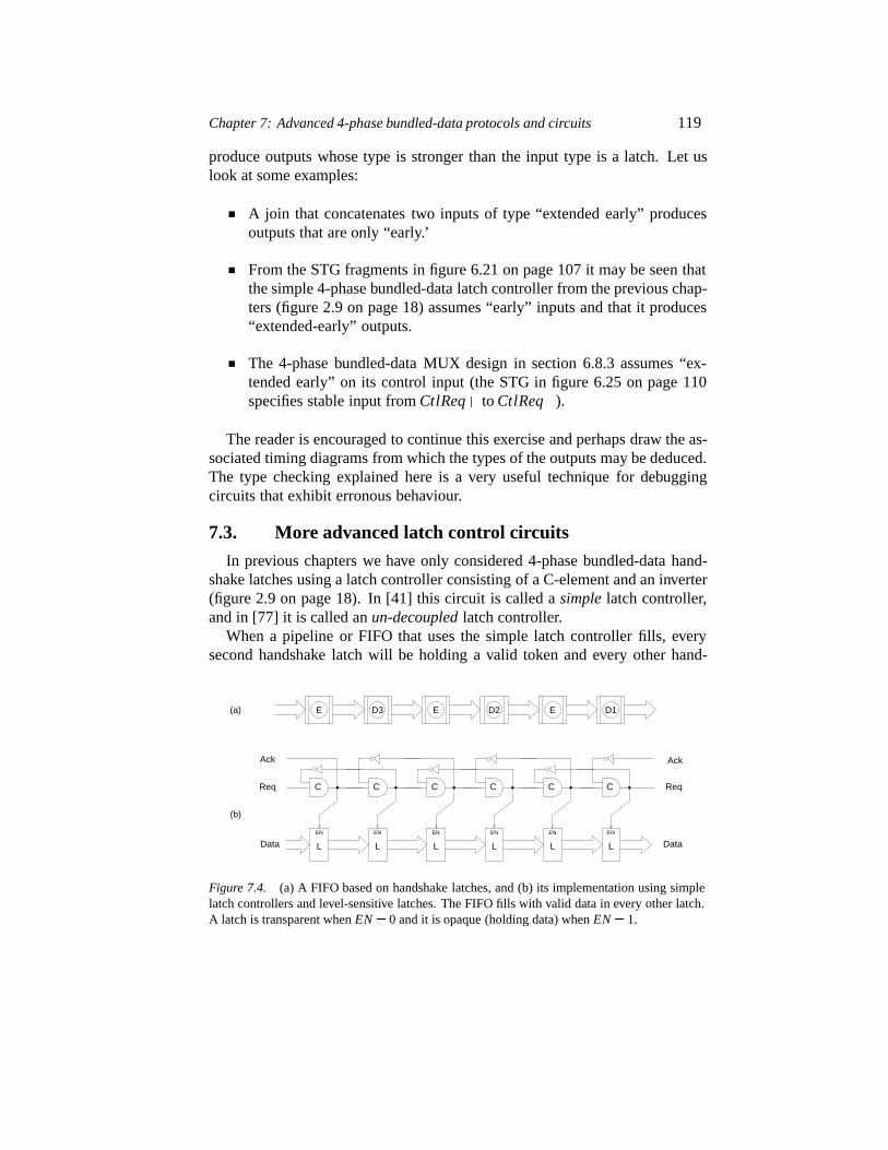
Chapter 7: Advanced 4-phase bundled-data protocols and circuits 119
produce outputs whose type is stronger than the input type is a latch. Let uslook at some examples:
A join that concatenates two inputs of type “extended early” producesoutputs that are only “early.’
From the STG fragments in figure 6.21 on page 107 it may be seen thatthe simple 4-phase bundled-data latch controller from the previous chap-ters (figure 2.9 on page 18) assumes “early” inputs and that it produces“extended-early” outputs.
The 4-phase bundled-data MUX design in section 6.8.3 assumes “ex-tended early” on its control input (the STG in figure 6.25 on page 110specifies stable input fromCtlReq� to CtlReq�).
The reader is encouraged to continue this exercise and perhaps draw the as-sociated timing diagrams from which the types of the outputs may be deduced.The type checking explained here is a very useful technique for debuggingcircuits that exhibit erronous behaviour.
7.3. More advanced latch control circuits
In previous chapters we have only considered 4-phase bundled-data hand-shake latches using a latch controller consisting of a C-element and an inverter(figure 2.9 on page 18). In [41] this circuit is called asimple latch controller,and in [77] it is called anun-decoupled latch controller.
When a pipeline or FIFO that uses the simple latch controller fills, everysecond handshake latch will be holding a valid token and every other hand-
EN
L
EN
L
EN
L
EN
L
EN
L
E D3 E E D1D2
Ack
Req
Data
Ack
Req
EN
L Data
(b)
(a)
C C C C C C
Figure 7.4. (a) A FIFO based on handshake latches, and (b) its implementation using simplelatch controllers and level-sensitive latches. The FIFO fills with valid data in every other latch.A latch is transparent whenEN � 0 and it is opaque (holding data) whenEN � 1.
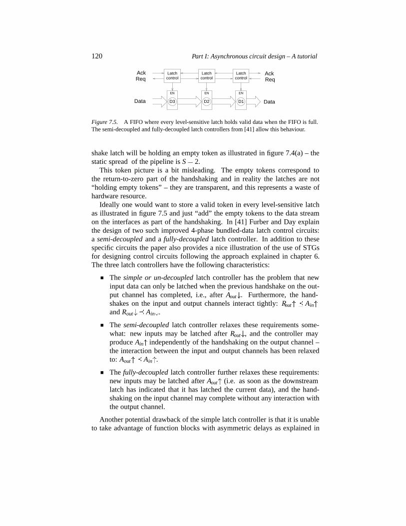
120 Part I: Asynchronous circuit design – A tutorial
AckReq
Data
AckReq
DataD3 D2 D1
EN EN EN
Latch Latch Latchcontrol control control
Figure 7.5. A FIFO where every level-sensitive latch holds valid data when the FIFO is full.The semi-decoupled and fully-decoupled latch controllers from [41] allow this behaviour.
shake latch will be holding an empty token as illustrated in figure 7.4(a) – thestatic spread of the pipeline isS � 2.
This token picture is a bit misleading. The empty tokens correspond tothe return-to-zero part of the handshaking and in reality the latches are not“holding empty tokens” – they are transparent, and this represents a waste ofhardware resource.
Ideally one would want to store a valid token in every level-sensitive latchas illustrated in figure 7.5 and just “add” the empty tokens to the data streamon the interfaces as part of the handshaking. In [41] Furber and Day explainthe design of two such improved 4-phase bundled-data latch control circuits:a semi-decoupled and afully-decoupled latch controller. In addition to thesespecific circuits the paper also provides a nice illustration of the use of STGsfor designing control circuits following the approach explained in chapter 6.The three latch controllers have the following characteristics:
The simple or un-decoupled latch controller has the problem that newinput data can only be latched when the previous handshake on the out-put channel has completed, i.e., afterAout . Furthermore, the hand-shakes on the input and output channels interact tightly:Rout � AinandRout � Ain .
The semi-decoupled latch controller relaxes these requirements some-what: new inputs may be latched afterRout , and the controller mayproduceAin independently of the handshaking on the output channel –the interaction between the input and output channels has been relaxedto: Aout � Ain.
The fully-decoupled latch controller further relaxes these requirements:new inputs may be latched afterAout (i.e. as soon as the downstreamlatch has indicated that it has latched the current data), and the hand-shaking on the input channel may complete without any interaction withthe output channel.
Another potential drawback of the simple latch controller is that it is unableto take advantage of function blocks with asymmetric delays as explained in
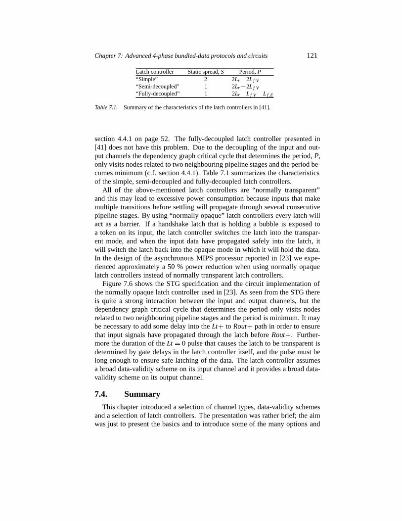
Chapter 7: Advanced 4-phase bundled-data protocols and circuits 121
Latch controller Static spread,S Period,P“Simple” 2 2Lr�2L f �V“Semi-decoupled” 1 2Lr�2L f �V“Fully-decoupled” 1 2Lr�L f �V �L f �E
Table 7.1. Summary of the characteristics of the latch controllers in [41].
section 4.4.1 on page 52. The fully-decoupled latch controller presented in[41] does not have this problem. Due to the decoupling of the input and out-put channels the dependency graph critical cycle that determines the period,P,only visits nodes related to two neighbouring pipeline stages and the period be-comes minimum (c.f. section 4.4.1). Table 7.1 summarizes the characteristicsof the simple, semi-decoupled and fully-decoupled latch controllers.
All of the above-mentioned latch controllers are “normally transparent”and this may lead to excessive power consumption because inputs that makemultiple transitions before settling will propagate through several consecutivepipeline stages. By using “normally opaque” latch controllers every latch willact as a barrier. If a handshake latch that is holding a bubble is exposed toa token on its input, the latch controller switches the latch into the transpar-ent mode, and when the input data have propagated safely into the latch, itwill switch the latch back into the opaque mode in which it will hold the data.In the design of the asynchronous MIPS processor reported in [23] we expe-rienced approximately a 50 % power reduction when using normally opaquelatch controllers instead of normally transparent latch controllers.
Figure 7.6 shows the STG specification and the circuit implementation ofthe normally opaque latch controller used in [23]. As seen from the STG thereis quite a strong interaction between the input and output channels, but thedependency graph critical cycle that determines the period only visits nodesrelated to two neighbouring pipeline stages and the period is minimum. It maybe necessary to add some delay into theLt� to Rout� path in order to ensurethat input signals have propagated through the latch beforeRout�. Further-more the duration of theLt � 0 pulse that causes the latch to be transparent isdetermined by gate delays in the latch controller itself, and the pulse must belong enough to ensure safe latching of the data. The latch controller assumesa broad data-validity scheme on its input channel and it provides a broad data-validity scheme on its output channel.
7.4. Summary
This chapter introduced a selection of channel types, data-validity schemesand a selection of latch controllers. The presentation was rather brief; the aimwas just to present the basics and to introduce some of the many options and
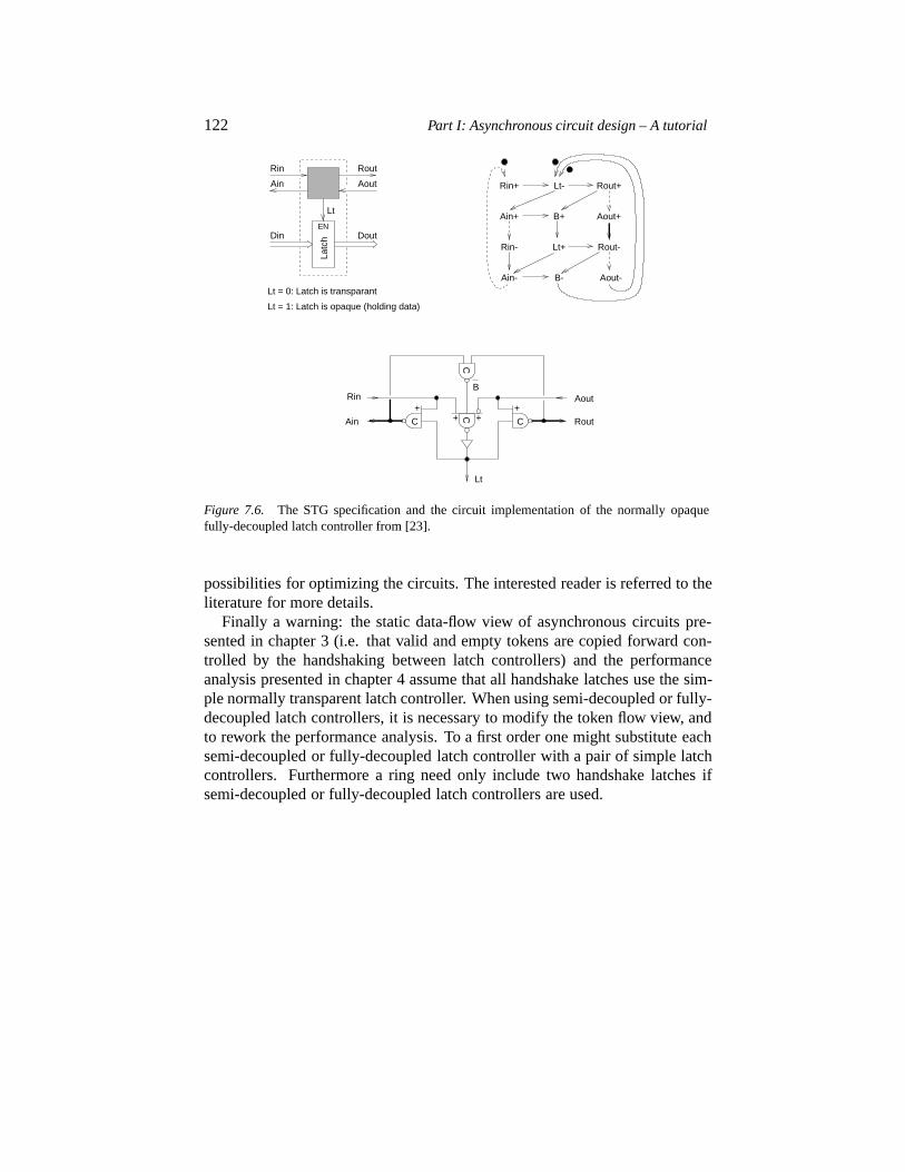
122 Part I: Asynchronous circuit design – A tutorial
Lt = 0: Latch is transparant
Lt = 1: Latch is opaque (holding data)
C
CC
C
++++
B
EN
Rin+ Rout+
Ain+
Rin-
Ain- Aout-
Rout-
Aout+
Lt-
B+
B-
Lt+
Lt
Rout
AoutRin
Ain
Latc
h
Lt
Rin
Ain
Rout
Aout
Din Dout
Figure 7.6. The STG specification and the circuit implementation of the normally opaquefully-decoupled latch controller from [23].
possibilities for optimizing the circuits. The interested reader is referred to theliterature for more details.
Finally a warning: the static data-flow view of asynchronous circuits pre-sented in chapter 3 (i.e. that valid and empty tokens are copied forward con-trolled by the handshaking between latch controllers) and the performanceanalysis presented in chapter 4 assume that all handshake latches use the sim-ple normally transparent latch controller. When using semi-decoupled or fully-decoupled latch controllers, it is necessary to modify the token flow view, andto rework the performance analysis. To a first order one might substitute eachsemi-decoupled or fully-decoupled latch controller with a pair of simple latchcontrollers. Furthermore a ring need only include two handshake latches ifsemi-decoupled or fully-decoupled latch controllers are used.
Chapter 8
HIGH-LEVEL LANGUAGES AND TOOLS
This chapter addresses languages and CAD tools for the high-level modelingand synthesis of asynchronous circuits. The aim is briefly to introduce somebasic concepts and a few representative and influential design methods. Theinterested reader will find more details elsewhere in this book (in Part II andchapter 13) as well as in the original papers that are cited in the text. In the lastsection we address the use of VHDL for the design of asynchronous circuits.
8.1. Introduction
Almost all work on the high-level modeling and synthesis of asynchronouscircuits is based on the use of a language that belongs to the CSP family oflanguages, rather than one of the two industry-standard hardware descriptionlanguages, VHDL and Verilog. Asynchronous circuits are highlyconcurrentand communication between modules is based onhandshake channels. Con-sequently a hardware description language for asynchronous circuit designshould provide efficient primitives supporting these two characteristics. TheCSP language proposed by Hoare [57, 58] meets these requirements. CSPstands for “Communicating Sequential Processes” and its key characteristicsare:
Concurrent processes.
Sequential and concurrent composition of statements within a process.
Synchronous message passing over point-to-point channels (supportedby the primitives send, receive and – possibly – probe).
CSP is a member of a large family of languages for programming concurrentsystems in general: OCCAM [68], LOTOS [108, 16], and CCS [89], as well aslanguages defined specifically for designing asynchronous circuits: Tangram[142, 135], CHP [81], and Balsa [9, 10]. Further details are presented else-where in this book on Tangram (in Part III, chapter 13) and Balsa (in Part II).
In this chapter we first take a closer look at the CSP language constructssupporting communication and concurrency. This will include a few sample
123
124 Part I: Asynchronous circuit design – A tutorial
programs to give a flavour of this type of language. Following this we brieflyexplain two rather different design methods that both take a CSP-like programas the starting point for the design:
At Philips Research Laboratories, van Berkel, Peeters, Kessels et al. havedeveloped a proprietary language, Tangram, and an associated siliconcompiler [142, 141, 135, 112]. Using a process called syntax-directedcompilation, the synthesis tool maps a Tangram program into a structureof handshake components. Using these tools several significant asyn-chronous chips have been designed within Philips [137, 138, 144, 73,74]. The last of these is a smart-card circuit that is described in chap-ter 13 on page 221.
At Caltech Martin has developed a language CHP – CommunicatingHardware Processes – and a set of tools that supports a partly manual,partly automated design flow that targets highly optimized transistor-level implementations of QDI 4-phase dual-rail circuits [80, 83].
CHP has a syntax that is similar to CSP (using various special symbols)whereas Tangram has a syntax that is more like a traditional programminglanguage (using keywords); but in essence they are both very similar to CSP.
In the last section of this chapter we will introduce a VHDL-package thatprovides CSP-like message passing and explain an associated VHDL-baseddesign flow that supports a manual step-wise refinement design process.
8.2. Concurrency and message passing in CSP
The “sequential processes” part of the CSP acronym denotes that each pro-cess is described by a program whose statements are executed in sequence oneby one. A semicolon is used to separate statements (as in many other program-ming languages). The semicolon can be seen as an operator that combinesstatements into programs. In this respect a process in CSP is very similar to aprocess in VHDL. However, CSP also allows the parallel composition of state-ments within a process. The symbol “�” denotes parallel composition. Thisfeature is not found in VHDL, whereas the fork-join construct in Verilog doesallow statement-level concurrency within a process.
The “communicating” part of the CSP acronym refers to synchronous mes-sage passing using point-to-point channels as illustrated in figure 8.1, wheretwo processesP1 andP2 are connected by a channel namedC. Using a sendstatement,C!x, processP1 sends (denoted by the ‘!’ symbol) the value of itsvariablex on channelC, and using a receive statement,C?y, processP2 re-ceives (denoted by the ‘?’ symbol) from channelC a value that is assignedto its variabley. The channel is memoryless and the transfer of the value ofvariablex in P1 into variabley in P2 is an atomic action. This has the effect
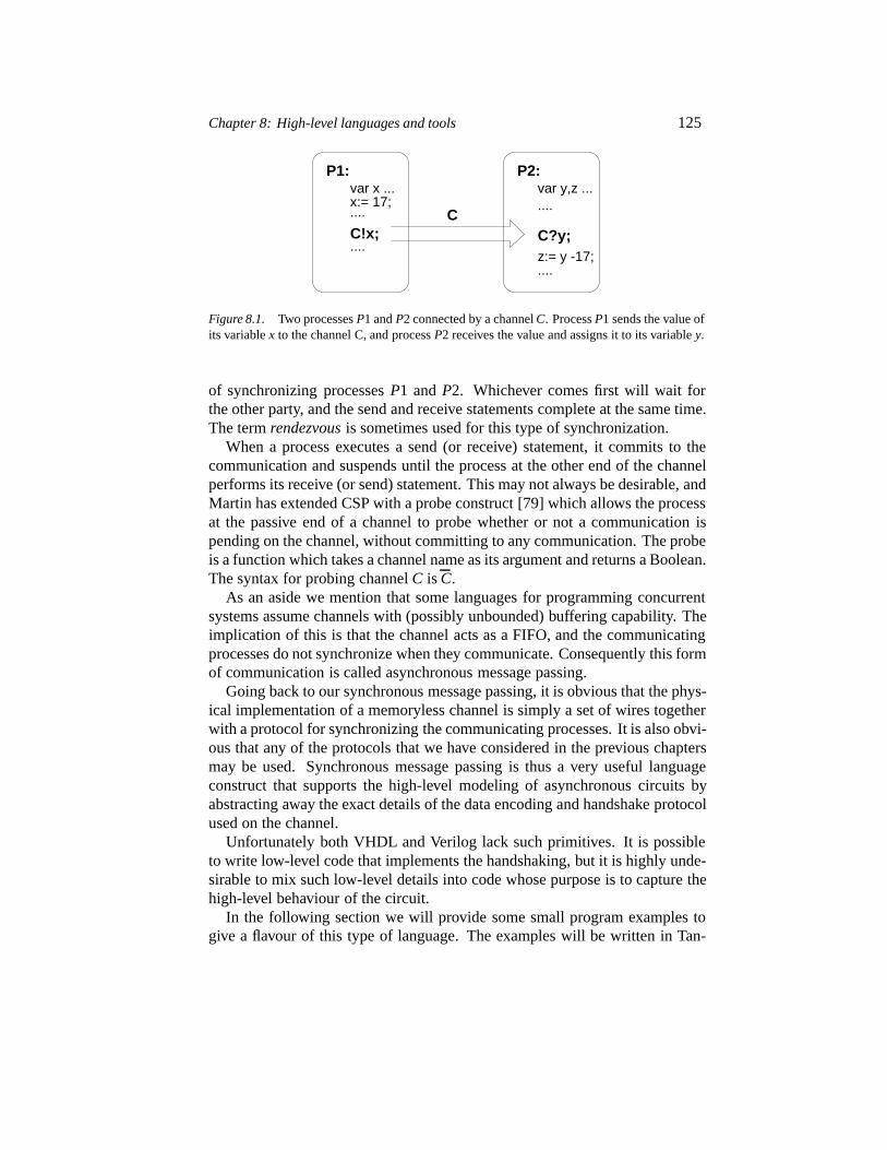
Chapter 8: High-level languages and tools 125
P2:
C
....C!x;....x:= 17;var x ...
P1:var y,z .......
C?y;z:= y -17;....
Figure 8.1. Two processesP1 andP2 connected by a channelC. ProcessP1 sends the value ofits variablex to the channel C, and processP2 receives the value and assigns it to its variabley.
of synchronizing processesP1 andP2. Whichever comes first will wait forthe other party, and the send and receive statements complete at the same time.The termrendezvous is sometimes used for this type of synchronization.
When a process executes a send (or receive) statement, it commits to thecommunication and suspends until the process at the other end of the channelperforms its receive (or send) statement. This may not always be desirable, andMartin has extended CSP with a probe construct [79] which allows the processat the passive end of a channel to probe whether or not a communication ispending on the channel, without committing to any communication. The probeis a function which takes a channel name as its argument and returns a Boolean.The syntax for probing channelC is C.
As an aside we mention that some languages for programming concurrentsystems assume channels with (possibly unbounded) buffering capability. Theimplication of this is that the channel acts as a FIFO, and the communicatingprocesses do not synchronize when they communicate. Consequently this formof communication is called asynchronous message passing.
Going back to our synchronous message passing, it is obvious that the phys-ical implementation of a memoryless channel is simply a set of wires togetherwith a protocol for synchronizing the communicating processes. It is also obvi-ous that any of the protocols that we have considered in the previous chaptersmay be used. Synchronous message passing is thus a very useful languageconstruct that supports the high-level modeling of asynchronous circuits byabstracting away the exact details of the data encoding and handshake protocolused on the channel.
Unfortunately both VHDL and Verilog lack such primitives. It is possibleto write low-level code that implements the handshaking, but it is highly unde-sirable to mix such low-level details into code whose purpose is to capture thehigh-level behaviour of the circuit.
In the following section we will provide some small program examples togive a flavour of this type of language. The examples will be written in Tan-
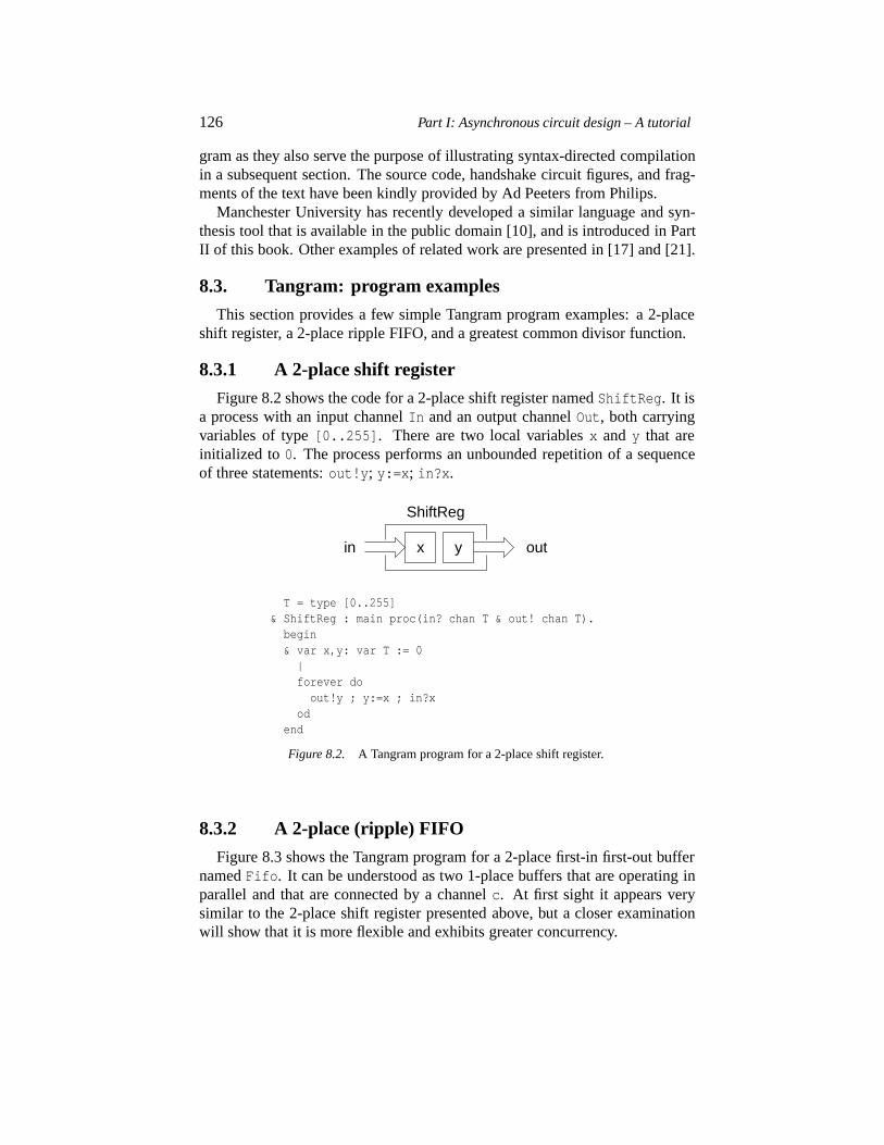
126 Part I: Asynchronous circuit design – A tutorial
gram as they also serve the purpose of illustrating syntax-directed compilationin a subsequent section. The source code, handshake circuit figures, and frag-ments of the text have been kindly provided by Ad Peeters from Philips.
Manchester University has recently developed a similar language and syn-thesis tool that is available in the public domain [10], and is introduced in PartII of this book. Other examples of related work are presented in [17] and [21].
8.3. Tangram: program examples
This section provides a few simple Tangram program examples: a 2-placeshift register, a 2-place ripple FIFO, and a greatest common divisor function.
8.3.1 A 2-place shift register
Figure 8.2 shows the code for a 2-place shift register namedShiftReg. It isa process with an input channelIn and an output channelOut, both carryingvariables of type[0..255]. There are two local variablesx and y that areinitialized to0. The process performs an unbounded repetition of a sequenceof three statements:out!y; y:=x; in?x.
x y out
ShiftReg
in
T = type [0..255]& ShiftReg : main proc(in? chan T & out! chan T).begin& var x,y: var T := 0
|forever doout!y ; y:=x ; in?x
odend
Figure 8.2. A Tangram program for a 2-place shift register.
8.3.2 A 2-place (ripple) FIFO
Figure 8.3 shows the Tangram program for a 2-place first-in first-out buffernamedFifo. It can be understood as two 1-place buffers that are operating inparallel and that are connected by a channelc. At first sight it appears verysimilar to the 2-place shift register presented above, but a closer examinationwill show that it is more flexible and exhibits greater concurrency.
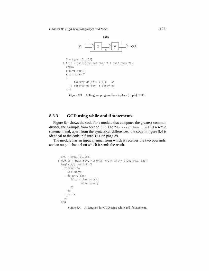
Chapter 8: High-level languages and tools 127
x yin out
Fifo
c
T = type [0..255]& Fifo : main proc(in? chan T & out! chan T).begin& x,y: var T& c : chan T|
forever do in?x ; c!x od|| forever do c?y ; out!y od
end
Figure 8.3. A Tangram program for a 2-place (ripple) FIFO.
8.3.3 GCD using while and if statements
Figure 8.4 shows the code for a module that computes the greatest commondivisor, the example from section 3.7. The “do x<>y then � � �od” is a whilestatement and, apart from the syntactical differences, the code in figure 8.4 isidentical to the code in figure 3.11 on page 39.
The module has an input channel from which it receives the two operands,and an output channel on which it sends the result.
int = type [0..255]& gcd_if : main proc (in?chan <<int,int>> & out!chan int).begin x,y:var int ff| forever do
in?<<x,y>>; do x<>y then
if x<y then y:=y-xelse x:=x-y
fiod
; out!xod
end
Figure 8.4. A Tangram for GCD using while and if statements.
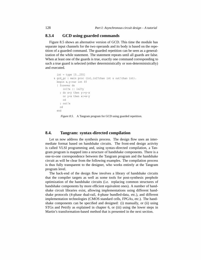
128 Part I: Asynchronous circuit design – A tutorial
8.3.4 GCD using guarded commands
Figure 8.5 shows an alternative version of GCD. This time the module hasseparate input channels for the two operands and its body is based on the repe-tition of a guarded command. The guarded repetition can be seen as a general-ization of the while statement. The statement repeats until all guards are false.When at least one of the guards is true, exactly one command corresponding tosuch a true guard is selected (either deterministically or non-deterministically)and executed.
int = type [0..255]& gcd_gc : main proc (in1,in2?chan int & out!chan int).begin x,y:var int ff| forever do
in1?x || in2?y; do x<y then y:=y-xor y<x then x:=x-yod
; out!xod
end
Figure 8.5. A Tangram program for GCD using guarded repetition.
8.4. Tangram: syntax-directed compilation
Let us now address the synthesis process. The design flow uses an inter-mediate format based on handshake circuits. The front-end design activityis called VLSI programming and, using syntax-directed compilation, a Tan-gram program is mapped into a structure of handshake components. There is aone-to-one correspondence between the Tangram program and the handshakecircuit as will be clear from the following examples. The compilation processis thus fully transparent to the designer, who works entirely at the Tangramprogram level.
The back-end of the design flow involves a library of handshake circuitsthat the compiler targets as well as some tools for post-synthesis peepholeoptimization of the handshake circuits (i.e. replacing common structures ofhandshake components by more efficient equivalent ones). A number of hand-shake circuit libraries exist, allowing implementations using different hand-shake protocols (4-phase dual-rail, 4-phase bundled-data, etc.), and differentimplementation technologies (CMOS standard cells, FPGAs, etc.). The hand-shake components can be specified and designed: (i) manually, or (ii) usingSTGs and Petrify as explained in chapter 6, or (iii) using the lower steps inMartin’s transformation-based method that is presented in the next section.
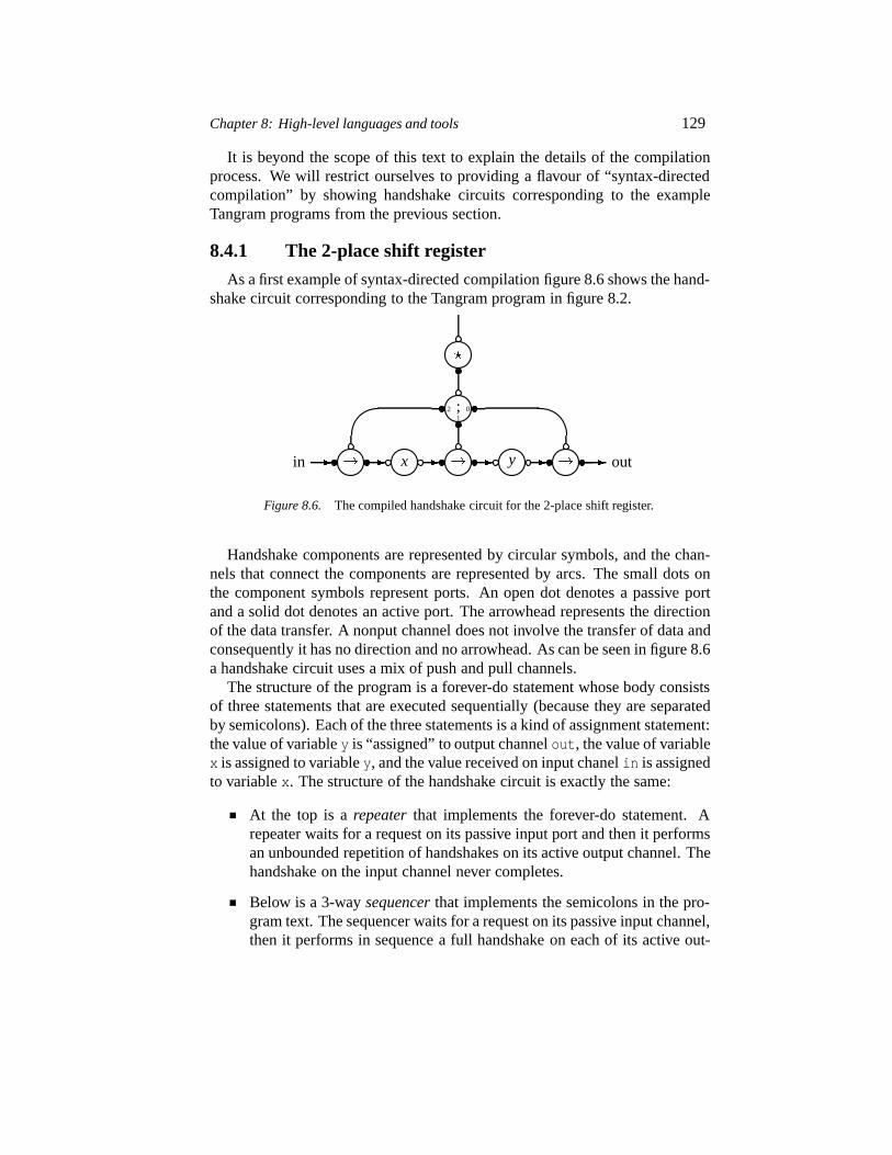
Chapter 8: High-level languages and tools 129
It is beyond the scope of this text to explain the details of the compilationprocess. We will restrict ourselves to providing a flavour of “syntax-directedcompilation” by showing handshake circuits corresponding to the exampleTangram programs from the previous section.
8.4.1 The 2-place shift register
As a first example of syntax-directed compilation figure 8.6 shows the hand-shake circuit corresponding to the Tangram program in figure 8.2.
�in �� ��x�
; 01
2
�
��y� � out
Figure 8.6. The compiled handshake circuit for the 2-place shift register.
Handshake components are represented by circular symbols, and the chan-nels that connect the components are represented by arcs. The small dots onthe component symbols represent ports. An open dot denotes a passive portand a solid dot denotes an active port. The arrowhead represents the directionof the data transfer. A nonput channel does not involve the transfer of data andconsequently it has no direction and no arrowhead. As can be seen in figure 8.6a handshake circuit uses a mix of push and pull channels.
The structure of the program is a forever-do statement whose body consistsof three statements that are executed sequentially (because they are separatedby semicolons). Each of the three statements is a kind of assignment statement:the value of variabley is “assigned” to output channelout, the value of variablex is assigned to variabley, and the value received on input chanelin is assignedto variablex. The structure of the handshake circuit is exactly the same:
At the top is arepeater that implements the forever-do statement. Arepeater waits for a request on its passive input port and then it performsan unbounded repetition of handshakes on its active output channel. Thehandshake on the input channel never completes.
Below is a 3-waysequencer that implements the semicolons in the pro-gram text. The sequencer waits for a request on its passive input channel,then it performs in sequence a full handshake on each of its active out-
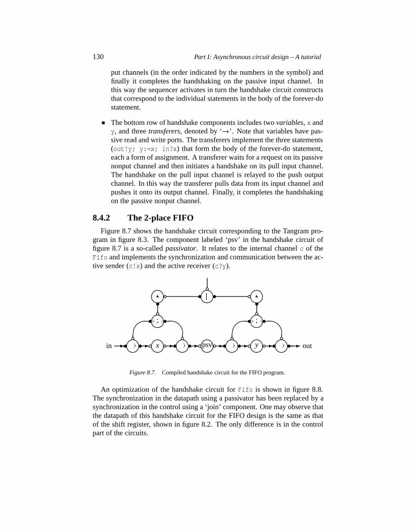
130 Part I: Asynchronous circuit design – A tutorial
put channels (in the order indicated by the numbers in the symbol) andfinally it completes the handshaking on the passive input channel. Inthis way the sequencer activates in turn the handshake circuit constructsthat correspond to the individual statements in the body of the forever-dostatement.
The bottom row of handshake components includes twovariables, x andy, and threetransferers, denoted by ‘�’. Note that variables have pas-sive read and write ports. The transferers implement the three statements(out!y; y:=x; in?x) that form the body of the forever-do statement,each a form of assignment. A transferer waits for a request on its passivenonput channel and then initiates a handshake on its pull input channel.The handshake on the pull input channel is relayed to the push outputchannel. In this way the transferer pulls data from its input channel andpushes it onto its output channel. Finally, it completes the handshakingon the passive nonput channel.
8.4.2 The 2-place FIFO
Figure 8.7 shows the handshake circuit corresponding to the Tangram pro-gram in figure 8.3. The component labeled ‘psv’ in the handshake circuit offigure 8.7 is a so-calledpassivator. It relates to the internal channelc of theFifo and implements the synchronization and communication between the ac-tive sender (c!x) and the active receiver (c?y).
�in
�
;0 1
�� ��x� psv�
� �
;0 1
�� ��y� � out
Figure 8.7. Compiled handshake circuit for the FIFO program.
An optimization of the handshake circuit forFifo is shown in figure 8.8.The synchronization in the datapath using a passivator has been replaced by asynchronization in the control using a ‘join’ component. One may observe thatthe datapath of this handshake circuit for the FIFO design is the same as thatof the shift register, shown in figure 8.2. The only difference is in the controlpart of the circuits.
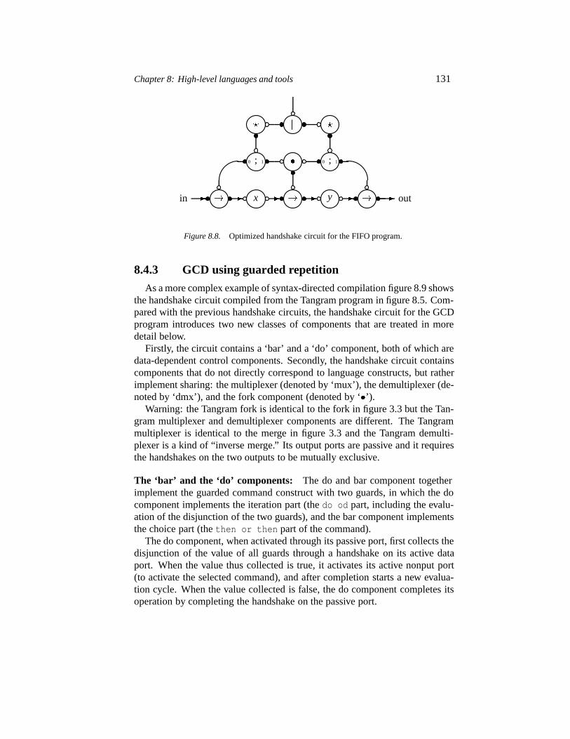
Chapter 8: High-level languages and tools 131
�in
�
;0 1
�� ��x�
�
� �
;0 1
��y� � out
Figure 8.8. Optimized handshake circuit for the FIFO program.
8.4.3 GCD using guarded repetition
As a more complex example of syntax-directed compilation figure 8.9 showsthe handshake circuit compiled from the Tangram program in figure 8.5. Com-pared with the previous handshake circuits, the handshake circuit for the GCDprogram introduces two new classes of components that are treated in moredetail below.
Firstly, the circuit contains a ‘bar’ and a ‘do’ component, both of which aredata-dependent control components. Secondly, the handshake circuit containscomponents that do not directly correspond to language constructs, but ratherimplement sharing: the multiplexer (denoted by ‘mux’), the demultiplexer (de-noted by ‘dmx’), and the fork component (denoted by ‘�’).
Warning: the Tangram fork is identical to the fork in figure 3.3 but the Tan-gram multiplexer and demultiplexer components are different. The Tangrammultiplexer is identical to the merge in figure 3.3 and the Tangram demulti-plexer is a kind of “inverse merge.” Its output ports are passive and it requiresthe handshakes on the two outputs to be mutually exclusive.
The ‘bar’ and the ‘do’ components: The do and bar component togetherimplement the guarded command construct with two guards, in which the docomponent implements the iteration part (thedo od part, including the evalu-ation of the disjunction of the two guards), and the bar component implementsthe choice part (thethen or then part of the command).
The do component, when activated through its passive port, first collects thedisjunction of the value of all guards through a handshake on its active dataport. When the value thus collected is true, it activates its active nonput port(to activate the selected command), and after completion starts a new evalua-tion cycle. When the value collected is false, the do component completes itsoperation by completing the handshake on the passive port.
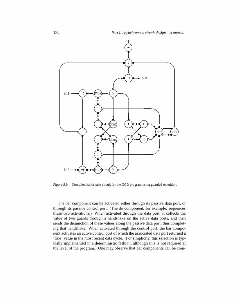
132 Part I: Asynchronous circuit design – A tutorial
��in2 mux
�� y�
�
� ��
dmx
�
�
�
���
��in1 mux
�
� x�
�
� �
�
dmx
�
�
�
�
�
�
bar ��
�do�
� � out�
;0 1
2
�
Figure 8.9. Compiled handshake circuit for the GCD program using guarded repetition.
The bar component can be activated either through its passive data port, orthrough its passive control port. (The do component, for example, sequencesthese two activations.) When activated through the data port, it collects thevalue of two guards through a handshake on the active data ports, and thensends the disjunction of these values along the passive data port, thus complet-ing that handshake. When activated through the control port, the bar compo-nent activates an active control port of which the associated data port returned a‘true’ value in the most recent data cycle. (For simplicity, this selection is typ-ically implemented in a deterministic fashion, although this is not required atthe level of the program.) One may observe that bar components can be com-
Chapter 8: High-level languages and tools 133
bined in a tree or list to implement a guarded command list of arbitrary length.Furthermore, not every data cycle has to be followed by a control cycle.
The ‘mux’, ‘demux’, and ‘fork’ components The program for GCD infigure 8.4 has two occurrences of variablex in which a value is written intox,namely input actionin1?x and assignmentx:=x-y. In the handshake circuitof figure 8.9, these two write actions for Tangram variablex are merged by themultiplexer component so as to arrive at the write port of handshake variablex.
Variable x occurs at five different locations in the program as an expres-sion, once in the output expressionout!x, twice in the guard expressionsx<yandy<x, and twice in the assignment expressionsx-y andy-x. These five in-spections of variablex could be implemented as five distinct read ports on thehandshake variablex, which is shown in the handshake circuit in [135, Fig. 2.7,p.34]. In figure 8.9, a different compilation is shown, in which handshake vari-ablex has three read ports:
A read port dedicated to the occurrence in the output action.
A read port dedicated to the guard expressions. Their evaluation ismu-tually inclusive, and hence can be combined using a synchronizing forkcomponent.
A read port dedicated to the assignment expressions. Their evaluation ismutually exclusive, and hence can be combined using a demultiplexer.
The GCD example is discussed in further detail in chapter 13.
8.5. Martin’s translation process
The work of Martin and his group at Caltech has made fundamental contri-butions to asynchronous design and it has influenced the work of many otherresearchers. The methods have been used at Caltech to design several sig-nificant chips, most recently and most notably an asynchronous MIPS R3000processor [88]. As the following presentation of the design flow hints, the de-sign process is elaborate and sophisticated and is probably only an option to aperson who has spent time with the Caltech group.
The mostly manual design process involves the following steps (semantics-preserving transformations):
(1) Process decomposition where each process is refined into a collectionof interacting simpler processes. This step is repeated until all processes aresimple enough to be dealt with in the next step in the process.
(2) Handshake expansion where each communication channel is replacedby explicit wires and where each communication action (e.g. send or receive)
134 Part I: Asynchronous circuit design – A tutorial
is replaced by the signal transitions required by the protocol that is being used.For example a receive statement such as:
C?y
is replaced by a sequence of simpler statements – for example:
�Creq�; y :� data; Cack ; ��Creq�; Cack
which is read as: “wait for request to go high”, “read the data”, “drive ac-knowledge high”, “wait for request to go low”, and “drive acknowledge low”.
At this level it may be necessary to add state variables and/or to reshufflesignal transitions in order to obtain a specification that satisfies a conditionsimilar to the CSC condition in chapter 6.
(3) Production rule expansion where each handshaking expansion is re-placed by a set of production rules (or guarded commands), for example:
a�b �� c and �b��c �� c
A production rule consist of a condition and an action, and the action is per-formed whenever the condition is true. As an aside we mention that the abovetwo production rules express the same as the set and reset functions for thesignalc on page 96. The production rules specify the behaviour of the internalsignals and output signals of the process. The production rules are themselvessimple concurrent processes and the guards must ensure that the signal tran-sitions occur in program order (i.e. that the semantics of the original CHPprogram are maintained). This may require strengthening the guards. Further-more, in order to obtain simpler circuit implementations, the guards may bemodified and made symmetric.
(4) Operator reduction where production rules are grouped into clusters andwhere each cluster is mapped onto a basic hardware component similar to ageneralized C-element. The above two production rules would be mapped intothe generalized C-element shown in figure 6.17 on page 100.
8.6. Using VHDL for asynchronous design
8.6.1 Introduction
In this section we will introduce a couple of VHDL packages that providethe designer with primitives for synchronous message passing between pro-cesses – similar to the constructs found in the CSP-family of languages (send,receive and probe).
The material was developed in an M.Sc. project and used in the design of a32-bit floating-point ALU using the IEEE floating-point number representation[110], and it has subsequently been used in a course on asynchronous circuit
Chapter 8: High-level languages and tools 135
design. Others, including [95, 118, 149, 78], have developed related VHDLpackages and approaches.
The channel packages introduced in the following support only one typeof channel, using a 32-bit 4-phase bundled-data push protocol. However, asVHDL allows the overloading of procedures and functions, it is straightfor-ward to define channels with arbitrary data types. All it takes is a little cut-and-paste editing. Providing support for protocols other than the 4-phase bundled-data push protocol will require more significant extensions to the packages.
8.6.2 VHDL versus CSP-type languages
The previous sections introduced several CSP-like hardware description lan-guages for asynchronous design. The advantages of these languages are theirsupport of concurrency and synchronous message passing, as well as a limitedand well-defined set of language constructs that makes syntax-directed compi-lation a relatively simple task.
Having said this there is nothing that prevents a designer from using oneof the industry standard languages VHDL (or Verilog) for the design of asyn-chronous circuits. In fact some of the fundamental concepts in these languages– concurrent processes and signal events – are “nice fits” with the modelingand design of asynchronous circuits. To illustrate this figure 8.10 shows howthe Tangram program from figure 8.2 could be expressed in plain VHDL. Inaddition to demonstrating the feasibility, the figure also highlights the limi-tations of VHDL when it comes to modeling asynchronous circuits: most ofthe code expresses low-level handshaking details, and this greatly clutters thedescription of the function of the circuit.
VHDL obviously lacks built-in primitives for synchronous message passingon channels similar to those found in CSP-like languages. Another feature ofthe CSP family of languages that VHDL lacks is statement-level concurrencywithin a process. On the other hand there are also some advantages of using anindustry standard hardware description language such as VHDL:
It is well supported by existing CAD tool frameworks that provide sim-ulators, pre-designed modules, mixed-mode simulation, and tools forsynthesis, layout and the back annotation of timing information.
The same simulator and test bench can be used throughout the entire de-sign process from the first high-level specification to the final implemen-tation in some target technology (for example a standard cell layout).
It is possible to perform mixed-mode simulations where some entitiesare modeled using behavioural specifications and others are implementedusing the components of the target technology.
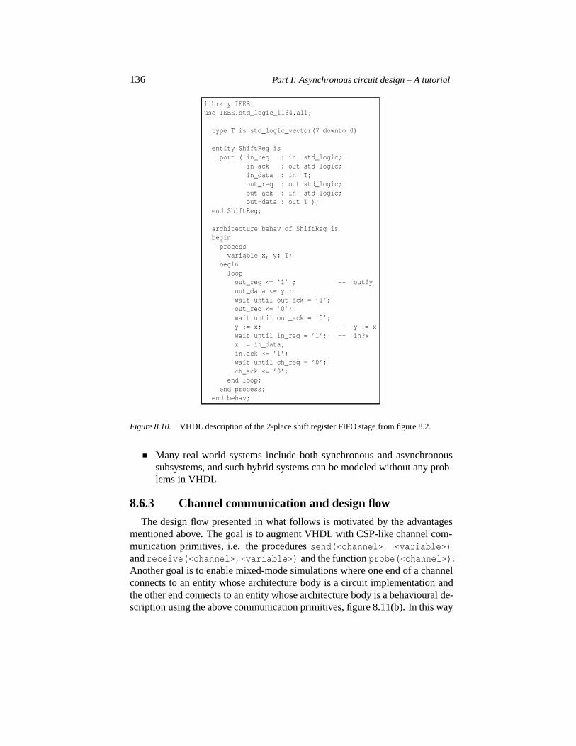
136 Part I: Asynchronous circuit design – A tutorial
library IEEE;use IEEE.std_logic_1164.all;
type T is std_logic_vector(7 downto 0)
entity ShiftReg isport ( in_req : in std_logic;
in_ack : out std_logic;in_data : in T;out_req : out std_logic;out_ack : in std_logic;out-data : out T );
end ShiftReg;
architecture behav of ShiftReg isbegin
processvariable x, y: T;
beginloopout_req <= ’1’ ; -- out!yout_data <= y ;wait until out_ack = ’1’;out_req <= ’0’;wait until out_ack = ’0’;y := x; -- y := xwait until in_req = ’1’; -- in?xx := in_data;in.ack <= ’1’;wait until ch_req = ’0’;ch_ack <= ’0’;
end loop;end process;
end behav;
Figure 8.10. VHDL description of the 2-place shift register FIFO stage from figure 8.2.
Many real-world systems include both synchronous and asynchronoussubsystems, and such hybrid systems can be modeled without any prob-lems in VHDL.
8.6.3 Channel communication and design flow
The design flow presented in what follows is motivated by the advantagesmentioned above. The goal is to augment VHDL with CSP-like channel com-munication primitives, i.e. the proceduressend(<channel>, <variable>)andreceive(<channel>,<variable>) and the functionprobe(<channel>).Another goal is to enable mixed-mode simulations where one end of a channelconnects to an entity whose architecture body is a circuit implementation andthe other end connects to an entity whose architecture body is a behavioural de-scription using the above communication primitives, figure 8.11(b). In this way
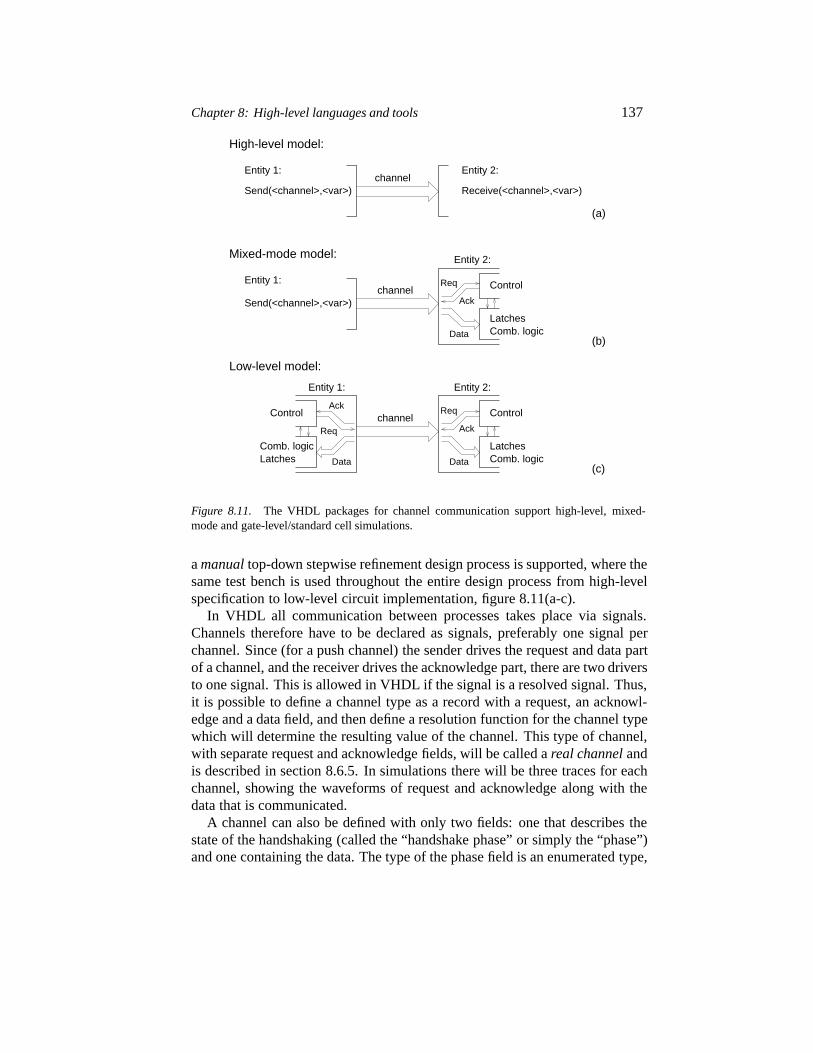
Chapter 8: High-level languages and tools 137
Data
Control
Latches
Ack
Req
Comb. logic
Entity 2:
High-level model:
Entity 2:
Receive(<channel>,<var>)channel
Data
Control
Latches
Ack
Req
Comb. logic
channel
Mixed-mode model: Entity 2:
Entity 1:
channel
Comb. logicLatches
Ack
Req
Data
Control
Low-level model:
Entity 1:
Send(<channel>,<var>)
Entity 1:
Send(<channel>,<var>)
(a)
(b)
(c)
Figure 8.11. The VHDL packages for channel communication support high-level, mixed-mode and gate-level/standard cell simulations.
amanual top-down stepwise refinement design process is supported, where thesame test bench is used throughout the entire design process from high-levelspecification to low-level circuit implementation, figure 8.11(a-c).
In VHDL all communication between processes takes place via signals.Channels therefore have to be declared as signals, preferably one signal perchannel. Since (for a push channel) the sender drives the request and data partof a channel, and the receiver drives the acknowledge part, there are two driversto one signal. This is allowed in VHDL if the signal is a resolved signal. Thus,it is possible to define a channel type as a record with a request, an acknowl-edge and a data field, and then define a resolution function for the channel typewhich will determine the resulting value of the channel. This type of channel,with separate request and acknowledge fields, will be called areal channel andis described in section 8.6.5. In simulations there will be three traces for eachchannel, showing the waveforms of request and acknowledge along with thedata that is communicated.
A channel can also be defined with only two fields: one that describes thestate of the handshaking (called the “handshake phase” or simply the “phase”)and one containing the data. The type of the phase field is an enumerated type,
138 Part I: Asynchronous circuit design – A tutorial
whose values can be the handshake phases a channel can assume, as well asthe values with which the sender and receiver can drive the field. This type ofchannel will be called anabstract channel. In simulations there will be twotraces for each channel, and it is easy to read the phases the channel assumesand the data values that are transfered.
The procedures and definitions are organized into two VHDL-packages: onecalled “abstpack.vhd” that can be used for simulating high-level models andone called “realpack.vhd” that can be used at all levels of design. Full listingscan be found in appendix 8.A at the end of this chapter. The design flowenabled by these packages is as follows:
The circuit and its environment or test bench is first modelled and sim-ulated using abstract channels. All it takes is the following statement inthe top level design unit: “usepackage work.abstpack.all”.
The circuit is then partitioned into simpler entities. The entities stillcommunicate using channels and the simulation still uses the abstractchannel package. This step may be repeated.
At some point the designer changes to using the real channel packageby changing to: “usepackage work.realpack.all” in the top-leveldesign unit. Apart from this simple change, the VHDL source code isidentical.
It is now possible to partition entities into control circuitry (that can bedesigned as explained in chapter 6) and data circuitry (that consist of or-dinary latches and combinational circuitry). Mixed mode simulations asillustrated in figure 8.11(b) are possible. Simulation models of the con-trol circuits may be their actual implementation in the target technologyor simply an entity containing a set of concurrent signal assignments –for example the Boolean equations produced by Petrify.
Eventually, when all entities have been partitioned into control and data,and when all leaf entities have been implemented using components ofthe target technology, the design is complete. Using standard technologymapping tools an implementation may be produced, and the circuit canbe simulated with back annotated timing information.
Note that the same simulation test bench can be used throughout the entiredesign process from the high-level specification to the low-level implementa-tion using components from the target technology.
8.6.4 The abstract channel package
An abstract channel is defined in figure 8.12 with a data type calledfp (a32-bit standard logic vector representing an IEEE floating-point number). The
Chapter 8: High-level languages and tools 139
type handshake_phase is(u, -- uninitializedidle, -- no communicationswait, -- sender waitingrwait, -- receiver waitingrcv, -- receiving datarec1, -- recovery phase 1rec2, -- recovery phase 2req, -- request signalack, -- acknowledge signalerror -- protocol error
);
subtype fp is std_logic_vector(31 downto 0);
type uchannel_fp isrecord
phase : handshake_phase;data : fp;
end record;
type uchannel_fp_vector is array(natural range <>) of uchannel_fp;
function resolved(s : uchannel_fp_vector) return uchannel_fp;
subtype channel_fp is resolved uchannel_fp;
Figure 8.12. Definition of an abstract channel.
actual channel type is calledchannel fp. It is necessary to define a channelfor each data type used in the design. The data type can be an arbitrary type,including record types, but it is advisable to use data types that are built fromstd logic because this is typically the type used by target component libraries(such as standard cell libraries) that are eventually used for the implementation.
The meaning of the values of the typehandshake phase are described indetail below:
u: Uninitialized channel. This is the default value of the drivers. As long aseither the sender or receiver drive the channel with this value, the channelstays uninitialized.
idle: No communication. Both the sender and receiver drive the channel withtheidle value.
swait: The sender is waiting to perform a communication. The sender is driv-ing the channel with thereq value and the receiver drives with theidlevalue.
rwait: The receiver is waiting to perform a communication. The sender isdriving the channel with theidle value and the receiver drives with the
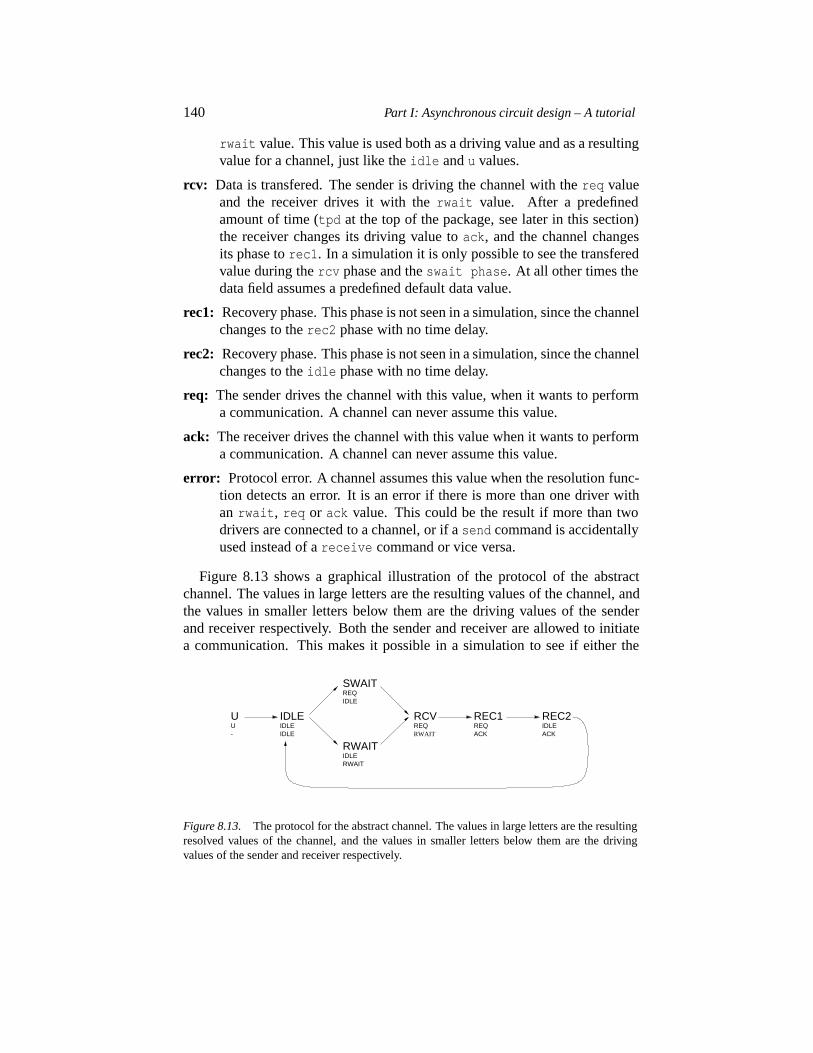
140 Part I: Asynchronous circuit design – A tutorial
rwait value. This value is used both as a driving value and as a resultingvalue for a channel, just like theidle andu values.
rcv: Data is transfered. The sender is driving the channel with thereq valueand the receiver drives it with therwait value. After a predefinedamount of time (tpd at the top of the package, see later in this section)the receiver changes its driving value toack, and the channel changesits phase torec1. In a simulation it is only possible to see the transferedvalue during thercv phase and theswait phase. At all other times thedata field assumes a predefined default data value.
rec1: Recovery phase. This phase is not seen in a simulation, since the channelchanges to therec2 phase with no time delay.
rec2: Recovery phase. This phase is not seen in a simulation, since the channelchanges to theidle phase with no time delay.
req: The sender drives the channel with this value, when it wants to performa communication. A channel can never assume this value.
ack: The receiver drives the channel with this value when it wants to performa communication. A channel can never assume this value.
error: Protocol error. A channel assumes this value when the resolution func-tion detects an error. It is an error if there is more than one driver withanrwait, req or ack value. This could be the result if more than twodrivers are connected to a channel, or if asend command is accidentallyused instead of areceive command or vice versa.
Figure 8.13 shows a graphical illustration of the protocol of the abstractchannel. The values in large letters are the resulting values of the channel, andthe values in smaller letters below them are the driving values of the senderand receiver respectively. Both the sender and receiver are allowed to initiatea communication. This makes it possible in a simulation to see if either the
IDLE
IDLE
RWAITIDLERWAIT
SWAITREQIDLE
RCVREQ
REC1REQACK
REC2IDLEACK-
UU
IDLERWAIT
Figure 8.13. The protocol for the abstract channel. The values in large letters are the resultingresolved values of the channel, and the values in smaller letters below them are the drivingvalues of the sender and receiver respectively.
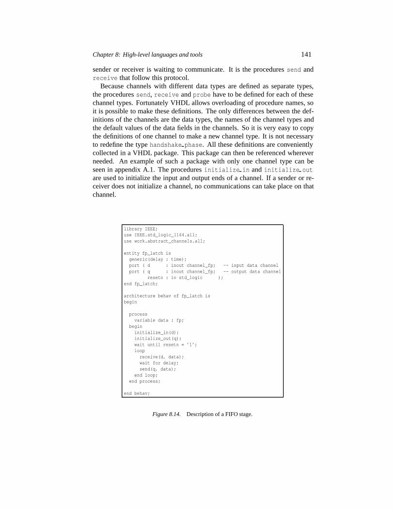
Chapter 8: High-level languages and tools 141
sender or receiver is waiting to communicate. It is the proceduressend andreceive that follow this protocol.
Because channels with different data types are defined as separate types,the proceduressend, receive andprobe have to be defined for each of thesechannel types. Fortunately VHDL allows overloading of procedure names, soit is possible to make these definitions. The only differences between the def-initions of the channels are the data types, the names of the channel types andthe default values of the data fields in the channels. So it is very easy to copythe definitions of one channel to make a new channel type. It is not necessaryto redefine the typehandshake phase. All these definitions are convenientlycollected in a VHDL package. This package can then be referenced whereverneeded. An example of such a package with only one channel type can beseen in appendix A.1. The proceduresinitialize in andinitialize outare used to initialize the input and output ends of a channel. If a sender or re-ceiver does not initialize a channel, no communications can take place on thatchannel.
library IEEE;use IEEE.std_logic_1164.all;use work.abstract_channels.all;
entity fp_latch isgeneric(delay : time);port ( d : inout channel_fp; -- input data channelport ( q : inout channel_fp; -- output data channel
resetn : in std_logic );end fp_latch;
architecture behav of fp_latch isbegin
processvariable data : fp;
begininitialize_in(d);initialize_out(q);wait until resetn = ’1’;loopreceive(d, data);wait for delay;send(q, data);
end loop;end process;
end behav;
Figure 8.14. Description of a FIFO stage.
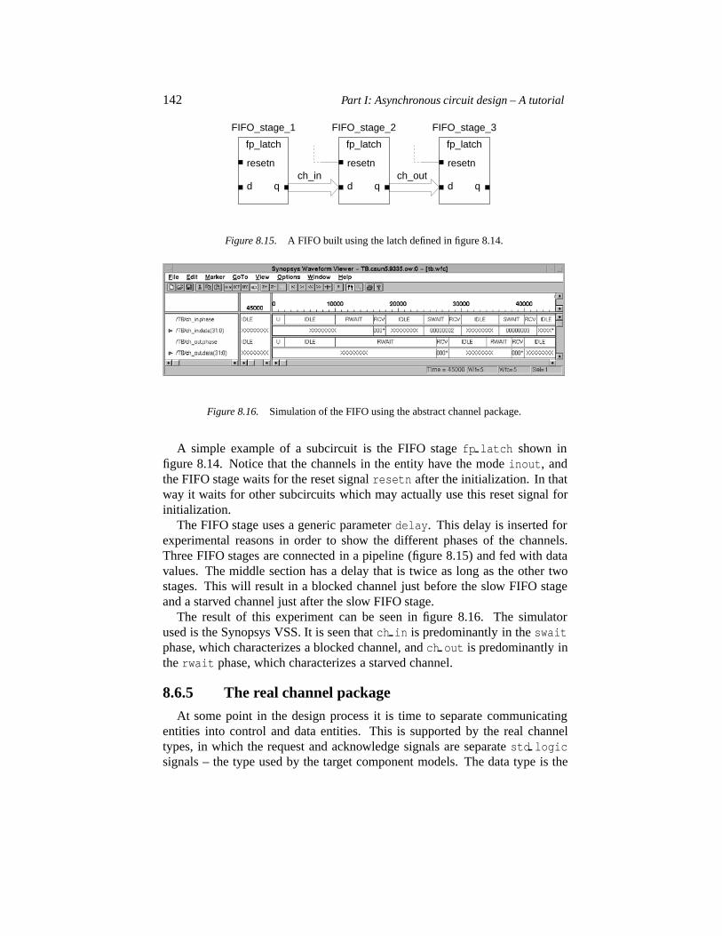
142 Part I: Asynchronous circuit design – A tutorial
d q
resetn
fp_latch
ch_in ch_outd q
resetn
fp_latch
d q
resetn
fp_latch
FIFO_stage_1 FIFO_stage_2 FIFO_stage_3
Figure 8.15. A FIFO built using the latch defined in figure 8.14.
Figure 8.16. Simulation of the FIFO using the abstract channel package.
A simple example of a subcircuit is the FIFO stagefp latch shown infigure 8.14. Notice that the channels in the entity have the modeinout, andthe FIFO stage waits for the reset signalresetn after the initialization. In thatway it waits for other subcircuits which may actually use this reset signal forinitialization.
The FIFO stage uses a generic parameterdelay. This delay is inserted forexperimental reasons in order to show the different phases of the channels.Three FIFO stages are connected in a pipeline (figure 8.15) and fed with datavalues. The middle section has a delay that is twice as long as the other twostages. This will result in a blocked channel just before the slow FIFO stageand a starved channel just after the slow FIFO stage.
The result of this experiment can be seen in figure 8.16. The simulatorused is the Synopsys VSS. It is seen thatch in is predominantly in theswaitphase, which characterizes a blocked channel, andch out is predominantly intherwait phase, which characterizes a starved channel.
8.6.5 The real channel package
At some point in the design process it is time to separate communicatingentities into control and data entities. This is supported by the real channeltypes, in which the request and acknowledge signals are separatestd logicsignals – the type used by the target component models. The data type is the
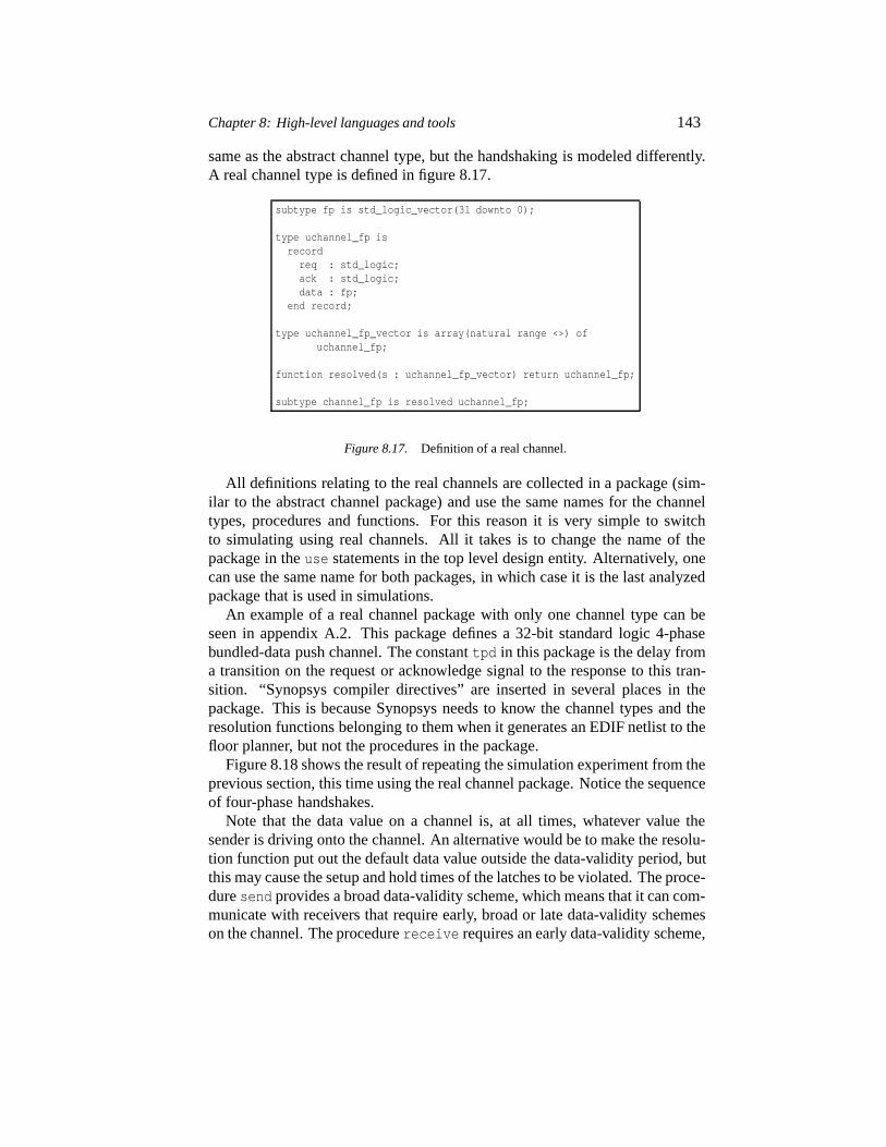
Chapter 8: High-level languages and tools 143
same as the abstract channel type, but the handshaking is modeled differently.A real channel type is defined in figure 8.17.
subtype fp is std_logic_vector(31 downto 0);
type uchannel_fp isrecord
req : std_logic;ack : std_logic;data : fp;
end record;
type uchannel_fp_vector is array(natural range <>) ofuchannel_fp;
function resolved(s : uchannel_fp_vector) return uchannel_fp;
subtype channel_fp is resolved uchannel_fp;
Figure 8.17. Definition of a real channel.
All definitions relating to the real channels are collected in a package (sim-ilar to the abstract channel package) and use the same names for the channeltypes, procedures and functions. For this reason it is very simple to switchto simulating using real channels. All it takes is to change the name of thepackage in theuse statements in the top level design entity. Alternatively, onecan use the same name for both packages, in which case it is the last analyzedpackage that is used in simulations.
An example of a real channel package with only one channel type can beseen in appendix A.2. This package defines a 32-bit standard logic 4-phasebundled-data push channel. The constanttpd in this package is the delay froma transition on the request or acknowledge signal to the response to this tran-sition. “Synopsys compiler directives” are inserted in several places in thepackage. This is because Synopsys needs to know the channel types and theresolution functions belonging to them when it generates an EDIF netlist to thefloor planner, but not the procedures in the package.
Figure 8.18 shows the result of repeating the simulation experiment from theprevious section, this time using the real channel package. Notice the sequenceof four-phase handshakes.
Note that the data value on a channel is, at all times, whatever value thesender is driving onto the channel. An alternative would be to make the resolu-tion function put out the default data value outside the data-validity period, butthis may cause the setup and hold times of the latches to be violated. The proce-duresend provides a broad data-validity scheme, which means that it can com-municate with receivers that require early, broad or late data-validity schemeson the channel. The procedurereceive requires an early data-validity scheme,
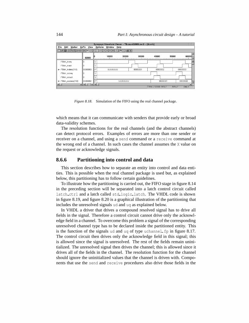
144 Part I: Asynchronous circuit design – A tutorial
Figure 8.18. Simulation of the FIFO using the real channel package.
which means that it can communicate with senders that provide early or broaddata-validity schemes.
The resolution functions for the real channels (and the abstract channels)can detect protocol errors. Examples of errors are more than one sender orreceiver on a channel, and using asend command or areceive command atthe wrong end of a channel. In such cases the channel assumes theX value onthe request or acknowledge signals.
8.6.6 Partitioning into control and data
This section describes how to separate an entity into control and data enti-ties. This is possible when the real channel package is used but, as explainedbelow, this partitioning has to follow certain guidelines.
To illustrate how the partitioning is carried out, the FIFO stage in figure 8.14in the preceding section will be separated into a latch control circuit calledlatch ctrl and a latch calledstd logic latch. The VHDL code is shownin figure 8.19, and figure 8.20 is a graphical illustration of the partitioning thatincludes the unresolved signalsud anduq as explained below.
In VHDL a driver that drives a compound resolved signal has to drive allfields in the signal. Therefore a control circuit cannot drive only the acknowl-edge field in a channel. To overcome this problem a signal of the correspondingunresolved channel type has to be declared inside the partitioned entity. Thisis the function of the signalsud anduq of type uchannel fp in figure 8.17.The control circuit then drives only the acknowledge field in this signal; thisis allowed since the signal is unresolved. The rest of the fields remain unini-tialized. The unresolved signal then drives the channel; this is allowed since itdrives all of the fields in the channel. The resolution function for the channelshould ignore the uninitialized values that the channel is driven with. Compo-nents that use thesend andreceive procedures also drive those fields in the
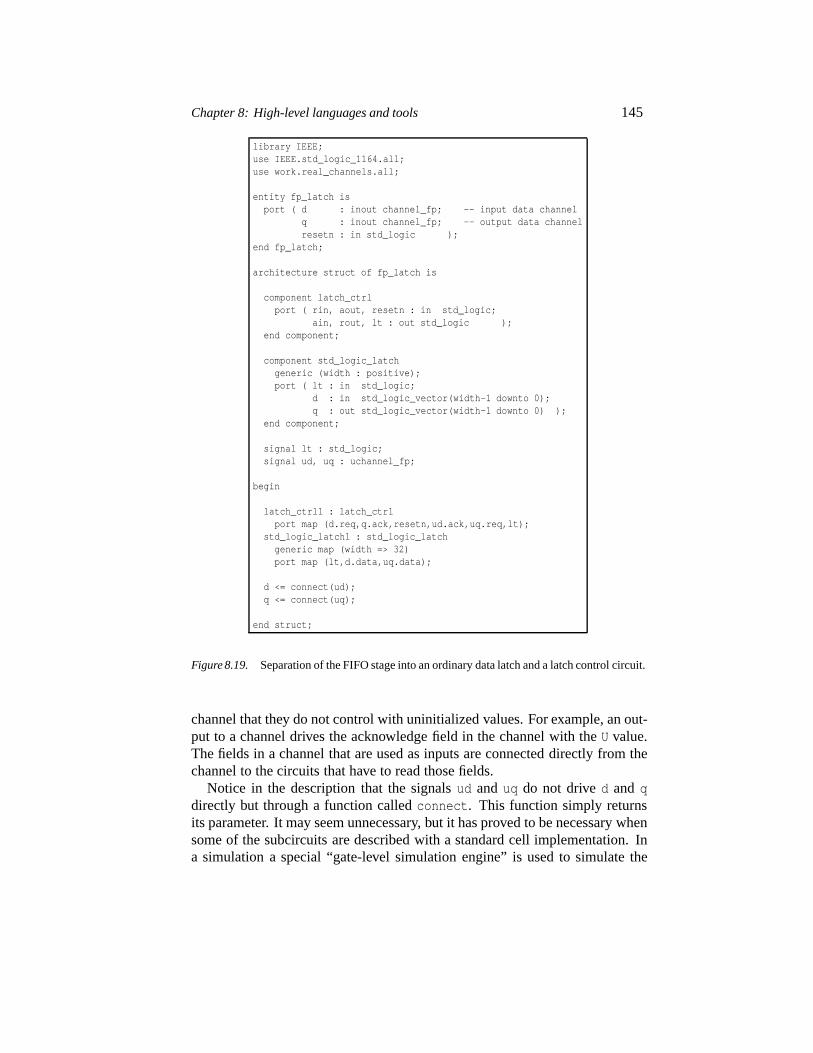
Chapter 8: High-level languages and tools 145
library IEEE;use IEEE.std_logic_1164.all;use work.real_channels.all;
entity fp_latch isport ( d : inout channel_fp; -- input data channel
q : inout channel_fp; -- output data channelresetn : in std_logic );
end fp_latch;
architecture struct of fp_latch is
component latch_ctrlport ( rin, aout, resetn : in std_logic;
ain, rout, lt : out std_logic );end component;
component std_logic_latchgeneric (width : positive);port ( lt : in std_logic;
d : in std_logic_vector(width-1 downto 0);q : out std_logic_vector(width-1 downto 0) );
end component;
signal lt : std_logic;signal ud, uq : uchannel_fp;
begin
latch_ctrl1 : latch_ctrlport map (d.req,q.ack,resetn,ud.ack,uq.req,lt);
std_logic_latch1 : std_logic_latchgeneric map (width => 32)port map (lt,d.data,uq.data);
d <= connect(ud);q <= connect(uq);
end struct;
Figure 8.19. Separation of the FIFO stage into an ordinary data latch and a latch control circuit.
channel that they do not control with uninitialized values. For example, an out-put to a channel drives the acknowledge field in the channel with theU value.The fields in a channel that are used as inputs are connected directly from thechannel to the circuits that have to read those fields.
Notice in the description that the signalsud anduq do not drived andqdirectly but through a function calledconnect. This function simply returnsits parameter. It may seem unnecessary, but it has proved to be necessary whensome of the subcircuits are described with a standard cell implementation. Ina simulation a special “gate-level simulation engine” is used to simulate the
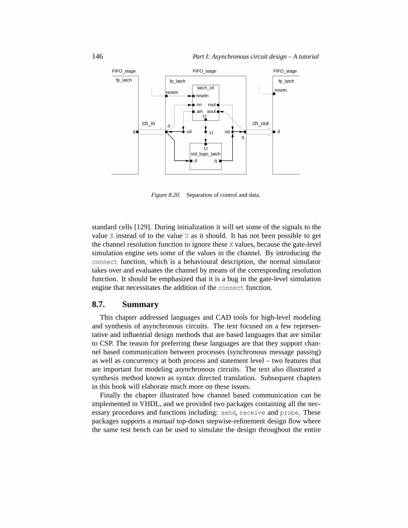
146 Part I: Asynchronous circuit design – A tutorial
Lt
d
std_logic_latch
q
d
resetn
Lt
Ltaoutain
rin rout
resetn
udq
uq
latch_ctl
ch_in ch_out
q
resetn
d
fp_latchfp_latch fp_latch
FIFO_stage FIFO_stage FIFO_stage
Figure 8.20. Separation of control and data.
standard cells [129]. During initialization it will set some of the signals to thevalueX instead of to the valueU as it should. It has not been possible to getthe channel resolution function to ignore theseX values, because the gate-levelsimulation engine sets some of the values in the channel. By introducing theconnect function, which is a behavioural description, the normal simulatortakes over and evaluates the channel by means of the corresponding resolutionfunction. It should be emphasized that it is a bug in the gate-level simulationengine that necessitates the addition of theconnect function.
8.7. Summary
This chapter addressed languages and CAD tools for high-level modelingand synthesis of asynchronous circuits. The text focused on a few represen-tative and influential design methods that are based languages that are similarto CSP. The reason for preferring these languages are that they support chan-nel based communication between processes (synchronous message passing)as well as concurrency at both process and statement level – two features thatare important for modeling asynchronous circuits. The text also illustrated asynthesis method known as syntax directed translation. Subsequent chaptersin this book will elaborate much more on these issues.
Finally the chapter illustrated how channel based communication can beimplemented in VHDL, and we provided two packages containing all the nec-essary procedures and functions including:send, receive andprobe. Thesepackages supports amanual top-down stepwise-refinement design flow wherethe same test bench can be used to simulate the design throughout the entire
Chapter 8: High-level languages and tools 147
design process from high level specification to low level circuit implementa-tion.
This chapter on languages and CAD-tools for asynchronous design con-cludes the tutorial on asynchronous circuit design and it it time to wrap up:Chapter 2 presented the fundamental concepts and theories, and provided point-ers to the literature. Chapters 3 and 4 presented an RTL-like abstract viewon asynchronous circuits (tokens flowing in static data-flow structures) that isvery useful for understanding their operation and performance. This materialis probably where this tutorial supplements the existing body of literature themost. Chapters 5 and 6 addressed the design of datapath operators and con-trol circuits. Focus in chapter 6 was on speed-independent circuits, but thisis not the only approach. In recent years there has also been great progressin synthesizing multiple-input-change fundamental-mode circuits. Chapter 7discussed more advanced 4-phase bundled-data protocols and circuits. Finallychapter 8 addressed languages and tools for high-level modeling and synthesisof asynchronous circuits.
The tutorial deliberately made no attempts at covering of all corners of thefield – the aim was to pave a road into “the world of asynchronous design”.Now you are here at the end of the road; hopefully with enough backgroundto carry on digging deeper into the literature, and equally importantly, withsufficient understanding of the characteristics of asynchronous circuits, thatyou can start designing your own circuits. And finally; asynchronous circuitsdo not represent an alternative to synchronous circuits. They have advantagesin some areas and disadvantages in other areas and they should be seen as asupplement, and as such they add new dimensions to the solution space thatthe digital designer explores. Even today, many circuits can not be categorizedas either synchronous or asynchronous, they contain elements of both.
The following chapters will introduce some recent industrial scale asyn-chronous chips. Additional designs are presented in [106].
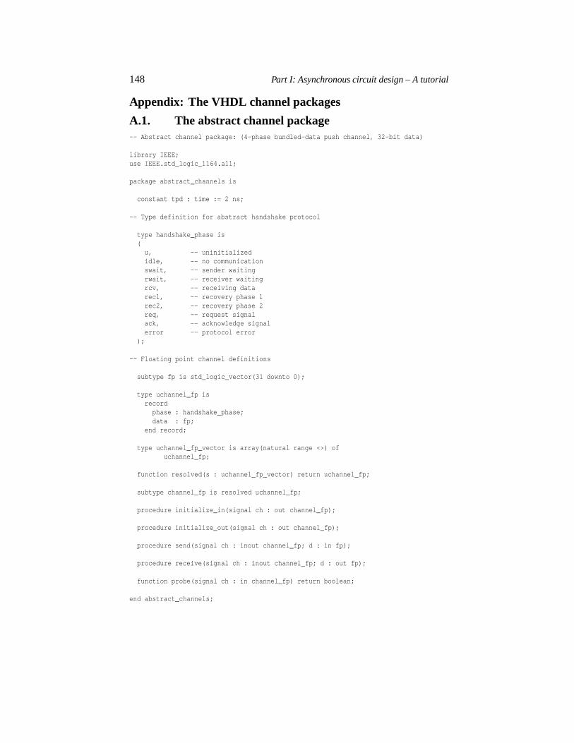
148 Part I: Asynchronous circuit design – A tutorial
Appendix: The VHDL channel packages
A.1. The abstract channel package-- Abstract channel package: (4-phase bundled-data push channel, 32-bit data)
library IEEE;use IEEE.std_logic_1164.all;
package abstract_channels is
constant tpd : time := 2 ns;
-- Type definition for abstract handshake protocol
type handshake_phase is(u, -- uninitializedidle, -- no communicationswait, -- sender waitingrwait, -- receiver waitingrcv, -- receiving datarec1, -- recovery phase 1rec2, -- recovery phase 2req, -- request signalack, -- acknowledge signalerror -- protocol error
);
-- Floating point channel definitions
subtype fp is std_logic_vector(31 downto 0);
type uchannel_fp isrecord
phase : handshake_phase;data : fp;
end record;
type uchannel_fp_vector is array(natural range <>) ofuchannel_fp;
function resolved(s : uchannel_fp_vector) return uchannel_fp;
subtype channel_fp is resolved uchannel_fp;
procedure initialize_in(signal ch : out channel_fp);
procedure initialize_out(signal ch : out channel_fp);
procedure send(signal ch : inout channel_fp; d : in fp);
procedure receive(signal ch : inout channel_fp; d : out fp);
function probe(signal ch : in channel_fp) return boolean;
end abstract_channels;
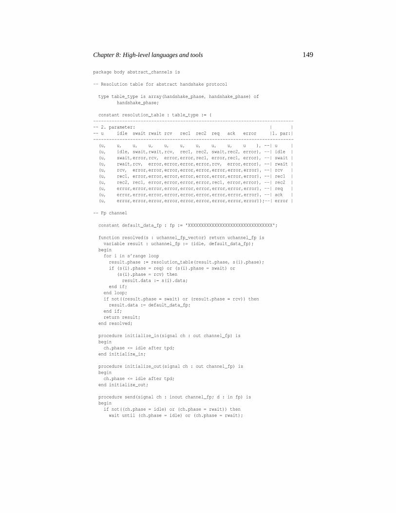
Chapter 8: High-level languages and tools 149
package body abstract_channels is
-- Resolution table for abstract handshake protocol
type table_type is array(handshake_phase, handshake_phase) ofhandshake_phase;
constant resolution_table : table_type := (------------------------------------------------------------------------------ 2. parameter: | |-- u idle swait rwait rcv rec1 rec2 req ack error |1. par:|----------------------------------------------------------------------------
(u, u, u, u, u, u, u, u, u, u ), --| u |(u, idle, swait,rwait,rcv, rec1, rec2, swait,rec2, error), --| idle |(u, swait,error,rcv, error,error,rec1, error,rec1, error), --| swait |(u, rwait,rcv, error,error,error,error,rcv, error,error), --| rwait |(u, rcv, error,error,error,error,error,error,error,error), --| rcv |(u, rec1, error,error,error,error,error,error,error,error), --| rec1 |(u, rec2, rec1, error,error,error,error,rec1, error,error), --| rec2 |(u, error,error,error,error,error,error,error,error,error), --| req |(u, error,error,error,error,error,error,error,error,error), --| ack |(u, error,error,error,error,error,error,error,error,error));--| error |
-- Fp channel
constant default_data_fp : fp := "XXXXXXXXXXXXXXXXXXXXXXXXXXXXXXXX";
function resolved(s : uchannel_fp_vector) return uchannel_fp isvariable result : uchannel_fp := (idle, default_data_fp);
beginfor i in s’range loop
result.phase := resolution_table(result.phase, s(i).phase);if (s(i).phase = req) or (s(i).phase = swait) or
(s(i).phase = rcv) thenresult.data := s(i).data;
end if;end loop;if not((result.phase = swait) or (result.phase = rcv)) then
result.data := default_data_fp;end if;return result;
end resolved;
procedure initialize_in(signal ch : out channel_fp) isbeginch.phase <= idle after tpd;
end initialize_in;
procedure initialize_out(signal ch : out channel_fp) isbeginch.phase <= idle after tpd;
end initialize_out;
procedure send(signal ch : inout channel_fp; d : in fp) isbeginif not((ch.phase = idle) or (ch.phase = rwait)) then
wait until (ch.phase = idle) or (ch.phase = rwait);
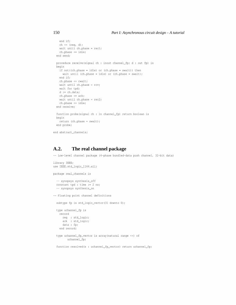
150 Part I: Asynchronous circuit design – A tutorial
end if;ch <= (req, d);wait until ch.phase = rec1;ch.phase <= idle;
end send;
procedure receive(signal ch : inout channel_fp; d : out fp) isbeginif not((ch.phase = idle) or (ch.phase = swait)) then
wait until (ch.phase = idle) or (ch.phase = swait);end if;ch.phase <= rwait;wait until ch.phase = rcv;wait for tpd;d := ch.data;ch.phase <= ack;wait until ch.phase = rec2;ch.phase <= idle;
end receive;
function probe(signal ch : in channel_fp) return boolean isbeginreturn (ch.phase = swait);
end probe;
end abstract_channels;
A.2. The real channel package-- Low-level channel package (4-phase bundled-data push channel, 32-bit data)
library IEEE;use IEEE.std_logic_1164.all;
package real_channels is
-- synopsys synthesis_offconstant tpd : time := 2 ns;-- synopsys synthesis_on
-- Floating point channel definitions
subtype fp is std_logic_vector(31 downto 0);
type uchannel_fp isrecord
req : std_logic;ack : std_logic;data : fp;
end record;
type uchannel_fp_vector is array(natural range <>) ofuchannel_fp;
function resolved(s : uchannel_fp_vector) return uchannel_fp;
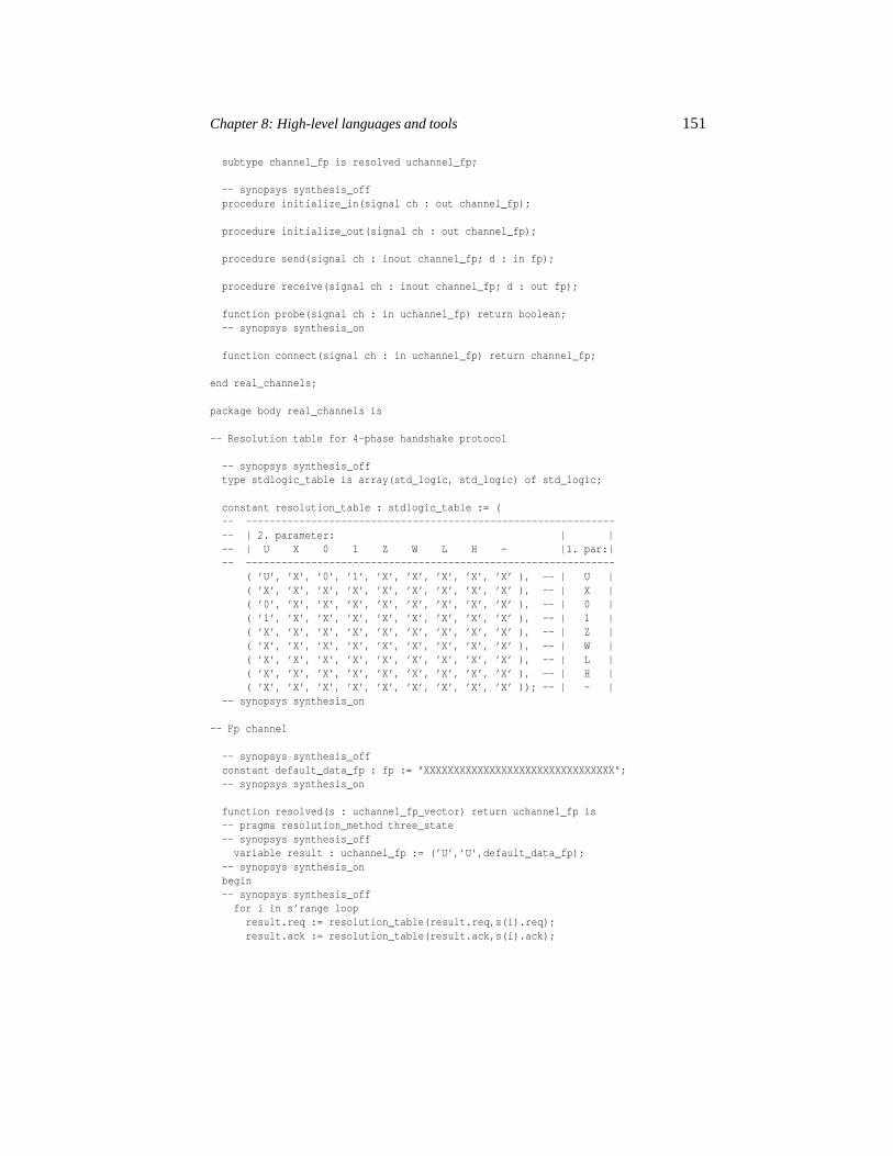
Chapter 8: High-level languages and tools 151
subtype channel_fp is resolved uchannel_fp;
-- synopsys synthesis_offprocedure initialize_in(signal ch : out channel_fp);
procedure initialize_out(signal ch : out channel_fp);
procedure send(signal ch : inout channel_fp; d : in fp);
procedure receive(signal ch : inout channel_fp; d : out fp);
function probe(signal ch : in uchannel_fp) return boolean;-- synopsys synthesis_on
function connect(signal ch : in uchannel_fp) return channel_fp;
end real_channels;
package body real_channels is
-- Resolution table for 4-phase handshake protocol
-- synopsys synthesis_offtype stdlogic_table is array(std_logic, std_logic) of std_logic;
constant resolution_table : stdlogic_table := (-- ---------------------------------------------------------------- | 2. parameter: | |-- | U X 0 1 Z W L H - |1. par:|-- --------------------------------------------------------------
( ’U’, ’X’, ’0’, ’1’, ’X’, ’X’, ’X’, ’X’, ’X’ ), -- | U |( ’X’, ’X’, ’X’, ’X’, ’X’, ’X’, ’X’, ’X’, ’X’ ), -- | X |( ’0’, ’X’, ’X’, ’X’, ’X’, ’X’, ’X’, ’X’, ’X’ ), -- | 0 |( ’1’, ’X’, ’X’, ’X’, ’X’, ’X’, ’X’, ’X’, ’X’ ), -- | 1 |( ’X’, ’X’, ’X’, ’X’, ’X’, ’X’, ’X’, ’X’, ’X’ ), -- | Z |( ’X’, ’X’, ’X’, ’X’, ’X’, ’X’, ’X’, ’X’, ’X’ ), -- | W |( ’X’, ’X’, ’X’, ’X’, ’X’, ’X’, ’X’, ’X’, ’X’ ), -- | L |( ’X’, ’X’, ’X’, ’X’, ’X’, ’X’, ’X’, ’X’, ’X’ ), -- | H |( ’X’, ’X’, ’X’, ’X’, ’X’, ’X’, ’X’, ’X’, ’X’ )); -- | - |
-- synopsys synthesis_on
-- Fp channel
-- synopsys synthesis_offconstant default_data_fp : fp := "XXXXXXXXXXXXXXXXXXXXXXXXXXXXXXXX";-- synopsys synthesis_on
function resolved(s : uchannel_fp_vector) return uchannel_fp is-- pragma resolution_method three_state-- synopsys synthesis_offvariable result : uchannel_fp := (’U’,’U’,default_data_fp);
-- synopsys synthesis_onbegin-- synopsys synthesis_offfor i in s’range loop
result.req := resolution_table(result.req,s(i).req);result.ack := resolution_table(result.ack,s(i).ack);
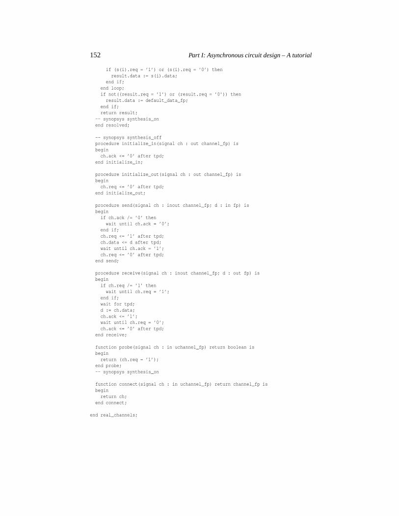
152 Part I: Asynchronous circuit design – A tutorial
if (s(i).req = ’1’) or (s(i).req = ’0’) thenresult.data := s(i).data;
end if;end loop;if not((result.req = ’1’) or (result.req = ’0’)) then
result.data := default_data_fp;end if;return result;
-- synopsys synthesis_onend resolved;
-- synopsys synthesis_offprocedure initialize_in(signal ch : out channel_fp) isbeginch.ack <= ’0’ after tpd;
end initialize_in;
procedure initialize_out(signal ch : out channel_fp) isbeginch.req <= ’0’ after tpd;
end initialize_out;
procedure send(signal ch : inout channel_fp; d : in fp) isbeginif ch.ack /= ’0’ then
wait until ch.ack = ’0’;end if;ch.req <= ’1’ after tpd;ch.data <= d after tpd;wait until ch.ack = ’1’;ch.req <= ’0’ after tpd;
end send;
procedure receive(signal ch : inout channel_fp; d : out fp) isbeginif ch.req /= ’1’ then
wait until ch.req = ’1’;end if;wait for tpd;d := ch.data;ch.ack <= ’1’;wait until ch.req = ’0’;ch.ack <= ’0’ after tpd;
end receive;
function probe(signal ch : in uchannel_fp) return boolean isbeginreturn (ch.req = ’1’);
end probe;-- synopsys synthesis_on
function connect(signal ch : in uchannel_fp) return channel_fp isbeginreturn ch;
end connect;
end real_channels;
II
BALSA - AN ASYNCHRONOUS HARDWARESYNTHESIS SYSTEM
Author: Doug Edwards, Andrew BardsleyDepartment of Computer ScienceThe University of Manchester{doug,bardsley}@cs.man.ac.uk
Abstract Balsa is a system for describing and synthesising asynchronous circuits basedon syntax-directed compilation into communicating handshake circuits. In thesechapters, the basic Balsa design flow is described and several simple circuit ex-amples are used to illustrate the Balsa language in an informal tutorial style. Thesection concludes with a walk-through of a major design exercise– a 4 channelDMA controller described entirely in Balsa.
Keywords: asynchronous circuits, high-level synthesis

Chapter 9
AN INTRODUCTION TO BALSA
9.1. Overview
Balsa is both a framework for synthesising asynchronous hardware systemsand a language for describing such systems. The approach adopted is that ofsyntax-directed compilation into communicating handshaking components andclosely follows the Tangram system ([141, 135] and Chapter 13 on page 221)of Philips. The advantage of this approach is that the compilation is trans-parent: there is a one-to-one mapping between the language constructs in thespecification and the intermediate handshake circuits that are produced. It isrelatively easy for an experienced user to envisage the micro-architecture of thecircuit that results from the original description. Incremental changes made atthe language level result in predictable changes at the circuit implementationlevel. This is important if optimisations and design trade-offs are to be madeeasily and contrasts with synchronous VHDL synthesis in which small changesin the specification may make radical alterations to the resulting circuit.
It is important to understand what Balsa offers the designer and what obli-gations are still placed upon the designer. The tight “edit description – syn-thesise – simulate – revise description” loop made possible by the fast com-pilation process makes it very easy for the design space of a system to beexplored and prototypes rapidly evaluated. However, there is no substitutefor creativity. Poor designs may be created as easily as elegant designs andsome experience in designing asynchronous circuits is required before even agood designer of conventional clocked circuits will best be able to exploit thesystem. Be warned that although Balsa guarantees correct-by-construction cir-cuits, it does not guarantee correct systems. In particular, it is quite feasible,as in any asynchronous system, to describe an elegant circuit which will ex-hibit deadlock. Furthermore, post-layout simulation is still required in orderto check that when the instantiated circuit has been placed and routed by con-ventional CAD tools, it meets basic timing requirements. On the other hand,a choice of implementation libraries is available allowing the designer to trade
155
156 Part II: Balsa - An Asynchronous HardwareSynthesis System
the greater process portability of a delay-insensitive implementation against,perhaps, smaller circuit area which may require a larger post-layout validationeffort.
Although Balsa has evolved from a research environment, it is not a toy sys-tem unsuited for large-scale designs; Balsa has been used to synthesise the 32channel DMA controller [11] for the Amulet3i asynchronous microprocessormacro-cell [48]. The controller has a complex specification and the resultingimplementation occupies 2mm2 on a 0�35µm 3-layer metal process. Balsa is atthe time of writing being used to synthesise a complete Amulet core as part ofthe EU funded G3 smartcard project [46].
As noted earlier, Balsa is very similar to Tangram. It is a less mature pack-age lacking some useful tools contained within the Tangram package such asthe power performance analyser. However, Balsa is freely available whereasTangram is not generally available outside Philips. As far as the expressivenessof the languages is concerned, Balsa adds powerful parameterisation using re-cursive expansion definition facilities whereas Tangram allows more flexibilityin interacting with non delay-insensitive external interfaces. Balsa has delib-erately chosen not to add such features to ensure that its channels-only delay-insensitive model is not compromised.
The reader should be aware that not all aspects of the Balsa language or itssyntax are explored in the material that follows: a more detailed introductionis available in the Balsa User Guide available from [7]. The Balsa system isfreely available from the same site. The system is still evolving: the descriptionhere refers to Balsa release 3.1.0.
9.2. Basic concepts
A circuit described in Balsa is compiled into a communicating network com-posed from a small (about 40) set of handshake components. The componentsare connected bychannels over which atomiccommunications or handshakestake place. Channels may have datapaths associated with them (in which casea handshake involves the transfer of data), or may be purely control (in whichcase the handshake acts as a synchronisation or rendezvous point).
Each channel connects exactly onepassive port of a handshake componentto oneactive port of another handshake component. An active port is a portwhich initiates a communication. A passive port responds (when it is ready) totherequest from the active port by anacknowledge signal.
Data channels may bepush channels orpull channels. In a push channel,the direction of the data flow is from the active port to the passive port. Thisis similar to the communication style of micropipelines. Data validity is sig-nalled by request and released on acknowledge. In a pull channel, the directionof data flow is from the passive port to the active port. The active port requests
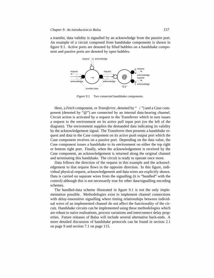
Chapter 9: An introduction to Balsa 157
a transfer, data validity is signalled by an acknowledge from the passive port.An example of a circuit composed from handshake components is shown infigure 9.1. Active ports are denoted by filled bubbles on a handshake compo-nent and passive ports are denoted by open bubbles.
acknowledge
requestacknowledge
request
acknowledge
bundled data
acknowledgerequest
request request
acknowledge
@
"0;1"
0
1
→
Figure 9.1. Two connected handshake components.
Here, aFetch component, orTransferrer, denoted by “� ”) and aCase com-ponent (denoted by “@”) are connected by an internal data-bearing channel.Circuit action is activated by a request to the Transferrer which in turn issuesa request to the environment on its active pull input port (on the left of thediagram). The environment supplies the demanded data indicating its validityby the acknowledgement signal. The Transferrer then presents a handshake re-quest and data to the Case component on its active push output port which theCase component receives on a passive port. Depending on the data value, theCase component issues a handshake to its environment on either the top rightor bottom right port. Finally, when the acknowledgement is received by theCase component, an acknowledgement is returned along the original channeland terminating this handshake. The circuit is ready to operate once more.
Data follows the direction of the request in this example and the acknowl-edgement to that request flows in the opposite direction. In this figure, indi-vidual physical request, acknowledgement and data wires are explicitly shown.Data is carried on separate wires from the signalling (it is “bundled” with thecontrol) although this is not necessarily true for other data/signalling encodingschemes.
The bundled-data scheme illustrated in figure 9.1 is not the only imple-mentation possible. Methodologies exist to implement channel connectionswith delay-insensitive signalling where timing relationships between individ-ual wires of an implemented channel do not affect the functionality of the cir-cuit. Handshake circuits can be implemented using these methodologies whichare robust to na¨ıve realisations, process variations and interconnect delay prop-erties. Future releases of Balsa will include several alternative back-ends. Amore detailed discussion of handshake protocols can be found in section 2.1on page 9 and section 7.1 on page 115.
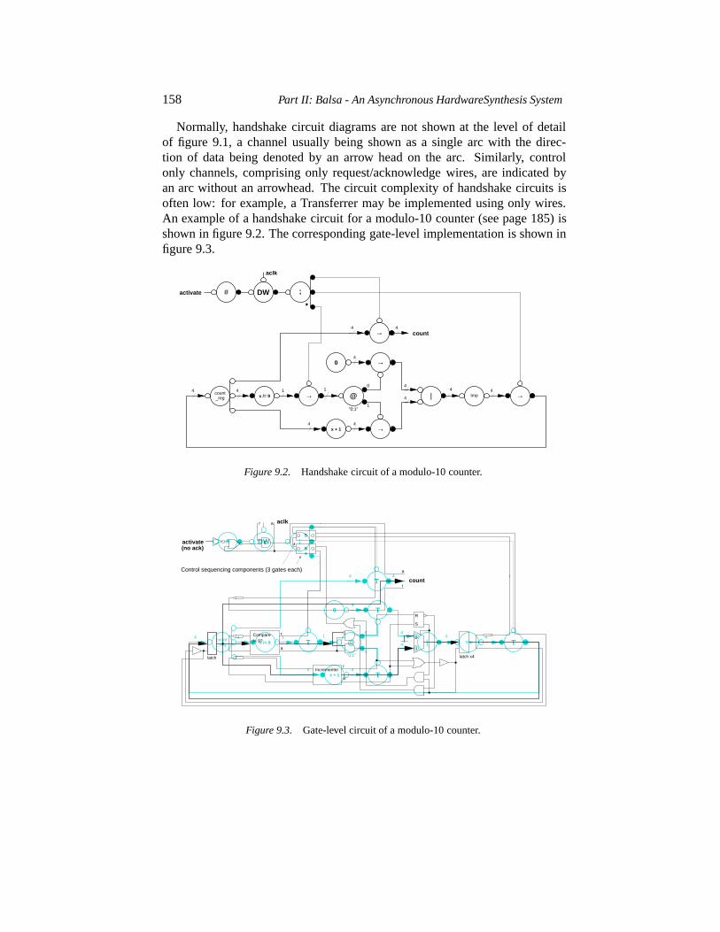
158 Part II: Balsa - An Asynchronous HardwareSynthesis System
Normally, handshake circuit diagrams are not shown at the level of detailof figure 9.1, a channel usually being shown as a single arc with the direc-tion of data being denoted by an arrow head on the arc. Similarly, controlonly channels, comprising only request/acknowledge wires, are indicated byan arc without an arrowhead. The circuit complexity of handshake circuits isoften low: for example, a Transferrer may be implemented using only wires.An example of a handshake circuit for a modulo-10 counter (see page 185) isshown in figure 9.2. The corresponding gate-level implementation is shown infigure 9.3.
count
aclk
activate
4
10
1
04
4
"0;1"
4
@ tmpx /= 94 count
_reg |
→
4→
→
→
→
44x + 1
14
# DW ;
*
44
Figure 9.2. Handshake circuit of a modulo-10 counter.
DW#
4 4
*
;
4 1
x + 14 4
T
T
@
"0;1"
10
1
T
T04
4
4
|4 4
tmp Tx /= 94 count
_reg
count
activate
aclk
(no ack)
Control sequencing components (3 gates each)
S
SC
r a
Compare r
a
/= 9?
Incrementerr
a
R
S
latch x4
r
a
0
1
latch
Figure 9.3. Gate-level circuit of a modulo-10 counter.
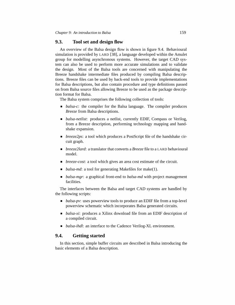
Chapter 9: An introduction to Balsa 159
9.3. Tool set and design flow
An overview of the Balsa design flow is shown in figure 9.4. Behaviouralsimulation is provided byLARD [38], a language developed within the Amuletgroup for modelling asynchronous systems. However, the target CAD sys-tem can also be used to perform more accurate simulations and to validatethe design. Most of the Balsa tools are concerned with manipulating theBreeze handshake intermediate files produced by compiling Balsa descrip-tions. Breeze files can be used by back-end tools to provide implementationsfor Balsa descriptions, but also contain procedure and type definitions passedon from Balsa source files allowing Breeze to be used as the package descrip-tion format for Balsa.
The Balsa system comprises the following collection of tools:
balsa-c: the compiler for the Balsa language. The compiler producesBreeze from Balsa descriptions.
balsa-netlist: produces a netlist, currently EDIF, Compass or Verilog,from a Breeze description, performing technology mapping and hand-shake expansion.
breeze2ps: a tool which produces a PostScript file of the handshake cir-cuit graph.
breeze2lard: a translator that converts aBreeze file to aLARD behaviouralmodel.
breeze-cost: a tool which gives an area cost estimate of the circuit.
balsa-md: a tool for generating Makefiles for make(1).
balsa-mgr: a graphical front-end tobalsa-md with project managementfacilities.
The interfaces between the Balsa and target CAD systems are handled bythe following scripts:
balsa-pv: uses powerview tools to produce an EDIF file from a top-levelpowerview schematic which incorporates Balsa generated circuits.
balsa-xi: produces a Xilinx download file from an EDIF description ofa compiled circuit.
balsa-ihdl: an interface to the Cadence Verilog-XL environment.
9.4. Getting started
In this section, simple buffer circuits are described in Balsa introducing thebasic elements of a Balsa description.
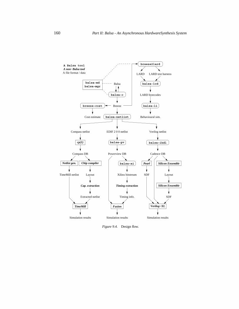
160 Part II: Balsa - An Asynchronous HardwareSynthesis System
balsa−c
balsa−netlist
breeze−cost
balsa−mdbalsa−mgr
balsa−li
balsa−lcd
breeze2lard
Behavioural sim.
LARD bytecodes
LARD test harnessLARD
balsa−pv
Fusion
balsa−xi
EDIF 2 0 0 netlist
Powerview DB
Simulation results
Xilinx bitstream
Timing extraction
Timing info.
balsa−ihdl
Pearl Silicon Ensemble
Silicon Ensemble
Verilog−XL
Verilog netlist
Cadence DB
SDF Layout
SDF
Simulation results
cp(1)
Chip compilerNetlist gen.
TimeMill
Compass netlist
Compass DB
Layout
Cap. extraction
Extracted netlist
TimeMill netlist
Simulation results
A non−Balsa toolA Balsa tool
A file format / data
Balsa
Breeze
Cost estimate
Figure 9.4. Design flow.
Chapter 9: An introduction to Balsa 161
9.4.1 A single-place buffer
This buffer circuit is the HDL equivalent of the “hello, world” program. ItsBalsa description is:
import [balsa.types.basic]-- a single line comment-- buffer1a: A single place bufferprocedure buffer1 (input i : byte; output o : byte) isvariable x : byte
beginloop
i -> x -- Input communication; -- sequence the two communicationso <- x -- Output communication
endend
Commentary on the code
This Balsa description builds a single-place buffer, 8-bits wide. The circuitrequests a byte from the environment which, when ready, transfers the datato the register. The circuit signals to the environment on its output channelthat data is available and the environment reads it when it chooses. This smallprogram introduces:
comments: Balsa supports both multi-line comments and single-line com-ments.
modular compilation: Balsa supports modular compilation. Theimportstatement in this example includes the definition of some standard data typessuch asbyte, nibble, etc. The search path given in theimport statementis a dot-separated directory path similar to that of Java (although multi-filepackages are not implemented). Theimport statement may be used to includeother precompiled Balsa programs thereby acting as a library mechanism. Anyimport statements must precede other declarations in the files.
procedures: Theprocedure declaration introduces an object that looks sim-ilar to a procedure definition in a conventional programming language. A Balsaprocedure is a process. The parameters of the procedure define the interface tothe environment outside the circuit block. In this case, the module has an 8-bitinput and an 8-bit output. The body of the procedure definition defines an al-gorithmic behaviour for the circuit; it also implies a structural implementation.In this example, a variablex (of typebyte) is declared implying that an 8-bitwide storage element will be appear in the synthesised circuit.
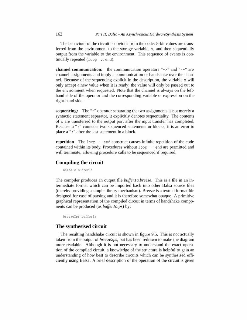
162 Part II: Balsa - An Asynchronous HardwareSynthesis System
The behaviour of the circuit is obvious from the code: 8-bit values are trans-ferred from the environment to the storage variable,x, and then sequentiallyoutput from the variable to the environment. This sequence of events is con-tinually repeated (loop � � � end).
channel communication: the communication operators “->” and “<-” arechannel assignments and imply a communication or handshake over the chan-nel. Because of the sequencing explicit in the description, the variablex willonly accept a new value when it is ready; the value will only be passed out tothe environment when requested. Note that the channel is always on the left-hand side of the operator and the corresponding variable or expression on theright-hand side.
sequencing: The “;” operator separating the two assignments is not merely asyntactic statement separator, it explicitly denotes sequentiality. The contentsof x are transferred to the output port after the input transfer has completed.Because a “;” connects two sequenced statements or blocks, it is an error toplace a “;” after the last statement in a block.
repetition Theloop � � � end construct causes infinite repetition of the codecontained within its body. Procedures withoutloop � � � end are permitted andwill terminate, allowing procedure calls to be sequenced if required.
Compiling the circuitbalsa-c buffer1a
The compiler produces an output filebuffer1a.breeze. This is a file in an in-termediate format which can be imported back into other Balsa source files(thereby providing a simple library mechanism). Breeze is a textual format filedesigned for ease of parsing and it is therefore somewhat opaque. A primitivegraphical representation of the compiled circuit in terms of handshake compo-nents can be produced (asbuffer1a.ps) by:
breeze2ps buffer1a
The synthesised circuit
The resulting handshake circuit is shown in figure 9.5. This is not actuallytaken from the output ofbreeze2ps, but has been redrawn to make the diagrammore readable. Although it is not necessary to understand the exact opera-tion of the compiled circuit, a knowledge of the structure is helpful to gain anunderstanding of how best to describe circuits which can be synthesised effi-ciently using Balsa. A brief description of the operation of the circuit is given
Chapter 9: An introduction to Balsa 163
oi
Loop
Sequence
Variable
→
➤
FetchFetch
→
*
x
;
#
Figure 9.5. Handshake circuit for a single-place buffer.
below. The circuit has been annotated with the names of the various handshakecomponents.
The port at the top, denoted by “>”, is anactivation port generating a hand-shake enclosing the behaviour of the circuit. It can be thought of as a resetsignal which, when de-asserted, initiates the operation of the circuit. All com-piled Balsa programs contain an activation port.
The activation port starts the operation of theRepeater (“#”) which initi-ates a handshake with theSequencer. The Repeater corresponds directly to theloop� � � end construct, and the Sequencer to the “;” operator. The Sequencerfirst issues a handshake to the left-handFetch component, causing data to bemoved to the storage element in theVariable element. The Sequencer thenhandshakes with the right-hand Fetch component, causing data to be read fromthe Variable element. When these operations are complete, the Sequencer com-pletes its handshake with the Repeater which starts the cycle again.
9.4.2 Two-place buffers
1st design
Having built a single-place buffer, an obvious goal is a pipeline of singlebuffer stages. Initially consider a two-place buffer; there are a number of wayswe might describe this. One choice is to define a circuit with two storageelements:
-- buffer2a: Sequential 2-place buffer with assignment-- between variablesimport [balsa.types.basic]
procedure buffer2 (input i : byte; output o : byte) isvariable x1, x2 : byte
begin
164 Part II: Balsa - An Asynchronous HardwareSynthesis System
loopi -> x1; -- Input communicationx2 := x1; -- Implied communicationo <- x2 -- Output communication
endend
In this example in we explicitly introduce two storage elements,x1 andx2.The contents of the variablex1 are caused to be transferred to the variablex2by means of the assignment operator “:=”. However, transfer is still effectedby means of a handshaking communication channel. This assignment operatoris merely a way of concealing the channel for convenience.
2nd design
The implicit channel can be made explicit as shown inbuffer2b.balsa:
-- buffer2b: Sequential version with an explicit-- internal channelimport [balsa.types.basic]
procedure buffer2 (input i:byte; output o:byte) isvariable x1, x2 : bytechannel chan: byte
beginloopi -> x1; -- Input communicationchan <- x1 || chan -> x2; -- Transfer x1 to x2o <- x2 -- Output communication
endend
The channel which, in the previous example, was concealed behind the useof the “:=” assignment operator, has been made explicit. The handshake circuitproduced (after some simple optimisations) is identical tobuffer2a. The “||”operator is explained in the next example.
It is important to understand the significance of the operation of the circuitsproduced bybuffer2a andbuffer2b. Remember that “;” is more than a syntac-tic separator: it is an operator denoting sequence. Thus, first the input,i, istransferred tox1. When this operation is complete,x1 is transferred tox2 andfinally the contents ofx2 are written to the environment on porto. Only afterthis sequence of operations is complete can new data from the environment beread intox1 again.
9.4.3 Parallel composition and module reuse
The operation above is unnecessarily constrained: there is no reason whythe circuit cannot be reading a new value intox1 at the same time thatx2 is
Chapter 9: An introduction to Balsa 165
writing out its data to the environment. The program inbuffer2c achieves thisoptimisation.
-- buffer2c: a 2-place buffer using parallel compositionimport [buffer1a]
procedure buffer2 (input i : byte; output o : byte) ischannel c : byte
beginbuffer1 (i, c) ||buffer1 (c, o)
end
Commentary on the code
In the program above, a 2-place buffer is composed from 2 single-placebuffers. The output of the first buffer is connected to the input of the secondbuffer by their respective output and input ports. However, apart from com-munications across the common channel, the operation of the two buffers isindependent.
The deceptively simple program above illustrates a number of new featuresof the Balsa language:
modular compilation: Thebuffer1a circuit is included by the import mech-anism described earlier. The circuit must have been compiled previously. TheMakefile generation programbalsa-md (see page 166) can be used to generatea Makefile which will automatically take care of such dependencies.
connectivity by naming: The output of the first buffer is connected to theinput of the second buffer because of the common channel name,c, in theparameter list in the instantiation of the buffers.
parallel composition: The “||” operator specifies that the two units which itconnects should operate in parallel. This does not mean that the two units mayoperate totally independently: in this example, the output of one buffer writesto the input of the other buffer, creating a point of synchronisation. Note alsothat the parallelism referred to is a temporal parallelism. The two buffers arephysically connected in series.
9.4.4 Placing multiple structures
If we wish to extend the number of places in the buffer, the previous tech-nique of explicitly enumerating every buffer becomes tedious. What is requiredis a means of parameterising the buffer length (though in any real hardwareimplementation the number of buffers cannot be variable and must be known
166 Part II: Balsa - An Asynchronous HardwareSynthesis System
before-hand). One technique, shown inbuffer n, is to use thefor constructtogether with compile-time constants:
-- buffer_n: an n-place parameterised bufferimport [buffer1a]constant n = 8
procedure buffer_n (input i:byte; output o:byte)is
array 1 .. n-1 of channel c : bytebegin
buffer1 (i, c[1]) || -- First bufferbuffer1 (c[n-1], o) || -- Last bufferfor || i in 1 .. n-2 then -- Buffer ibuffer1 (c[i], c[i+1])
endend
Commentary on the Code
constants: the value of an expression (of any type) may be bound to a name.The value of the expression is evaluated at compile time and the type of thename when used will be the same as the original expression in the constantdeclaration. Numbers can be given in decimal (starting with one of 1..9), hexa-decimal (0x prefix), octal (0 prefix) and binary (0b prefix).
arrayed channels: procedure ports and locally declared channels may bearrayed. Each channel can be referred to by a numeric or enumerated index,but from the point of view of handshaking, each channel is distinct and noindexed channel has any relationship with any other such channel other thanthe name they share. Arraying is not part of a channel’s type.
for loops: a for loop allows iteration over the instantiation of a subcircuit.The composition of the circuits may either be a parallel composition – as in theexample above – or sequential. In the latter case, “;” should be substituted for“||” in the loop specifier. The iteration range of the loop must be resolvable atcompile time.
A more flexible approach uses parameterised procedures and is discussedlater in chapter 11 on page 193.
9.5. Ancillary Balsa tools
9.5.1 Makefile generation
Makefiles are commonly used in Unix by the utility make(1) to specify andcontrol the processes by which complicated programs are compiled. Speci-fying the dependencies involved is often tedious and error prone. The Balsa
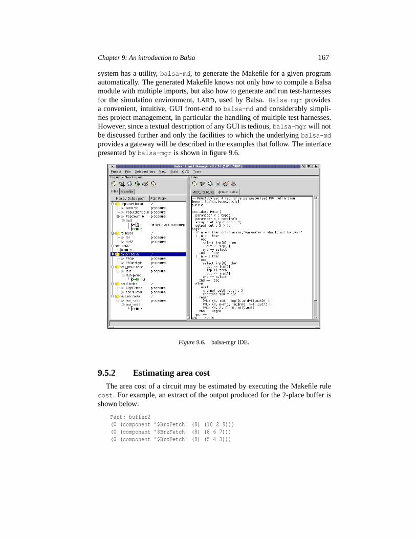
Chapter 9: An introduction to Balsa 167
system has a utility,balsa-md, to generate the Makefile for a given programautomatically. The generated Makefile knows not only how to compile a Balsamodule with multiple imports, but also how to generate and run test-harnessesfor the simulation environment,LARD, used by Balsa.Balsa-mgr providesa convenient, intuitive, GUI front-end tobalsa-md and considerably simpli-fies project management, in particular the handling of multiple test harnesses.However, since a textual description of any GUI is tedious,balsa-mgr will notbe discussed further and only the facilities to which the underlyingbalsa-mdprovides a gateway will be described in the examples that follow. The interfacepresented bybalsa-mgr is shown in figure 9.6.
Figure 9.6. balsa-mgr IDE.
9.5.2 Estimating area cost
The area cost of a circuit may be estimated by executing the Makefile rulecost. For example, an extract of the output produced for the 2-place buffer isshown below:
Part: buffer2(0 (component "$BrzFetch" (8) (10 2 9)))(0 (component "$BrzFetch" (8) (8 6 7)))(0 (component "$BrzFetch" (8) (5 4 3)))
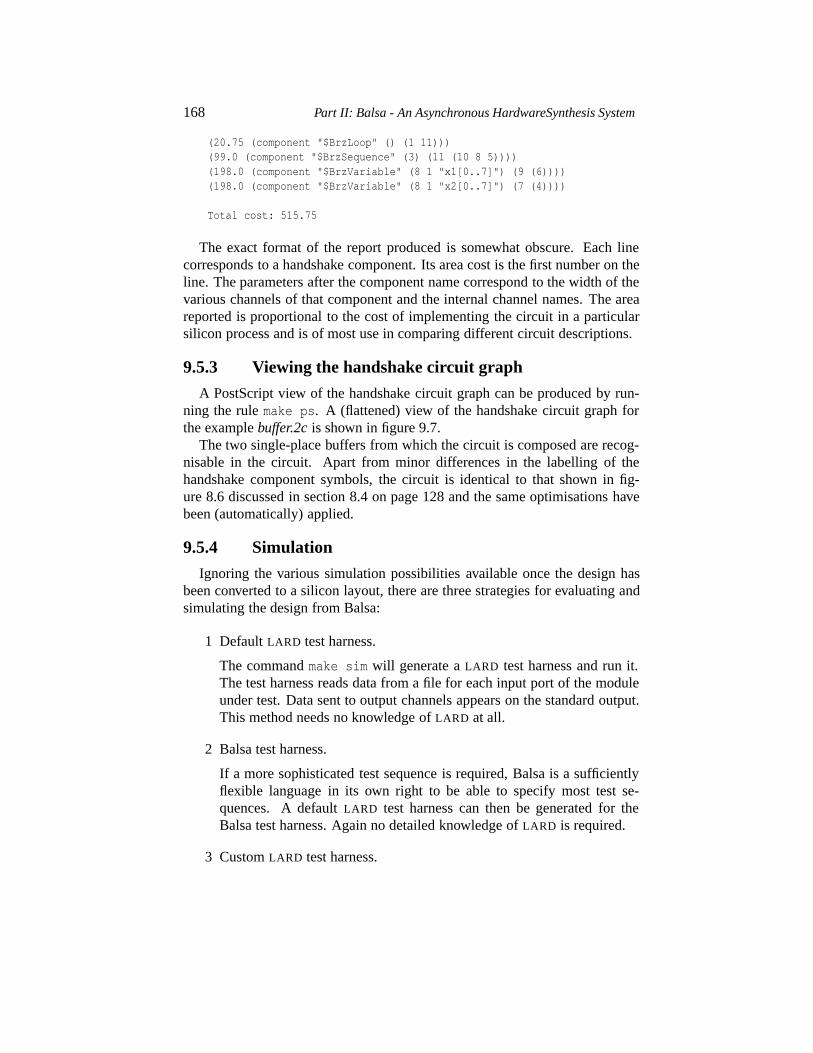
168 Part II: Balsa - An Asynchronous HardwareSynthesis System
(20.75 (component "$BrzLoop" () (1 11)))(99.0 (component "$BrzSequence" (3) (11 (10 8 5))))(198.0 (component "$BrzVariable" (8 1 "x1[0..7]") (9 (6))))(198.0 (component "$BrzVariable" (8 1 "x2[0..7]") (7 (4))))
Total cost: 515.75
The exact format of the report produced is somewhat obscure. Each linecorresponds to a handshake component. Its area cost is the first number on theline. The parameters after the component name correspond to the width of thevarious channels of that component and the internal channel names. The areareported is proportional to the cost of implementing the circuit in a particularsilicon process and is of most use in comparing different circuit descriptions.
9.5.3 Viewing the handshake circuit graph
A PostScript view of the handshake circuit graph can be produced by run-ning the rulemake ps. A (flattened) view of the handshake circuit graph forthe examplebuffer.2c is shown in figure 9.7.
The two single-place buffers from which the circuit is composed are recog-nisable in the circuit. Apart from minor differences in the labelling of thehandshake component symbols, the circuit is identical to that shown in fig-ure 8.6 discussed in section 8.4 on page 128 and the same optimisations havebeen (automatically) applied.
9.5.4 Simulation
Ignoring the various simulation possibilities available once the design hasbeen converted to a silicon layout, there are three strategies for evaluating andsimulating the design from Balsa:
1 DefaultLARD test harness.
The commandmake sim will generate aLARD test harness and run it.The test harness reads data from a file for each input port of the moduleunder test. Data sent to output channels appears on the standard output.This method needs no knowledge ofLARD at all.
2 Balsa test harness.
If a more sophisticated test sequence is required, Balsa is a sufficientlyflexible language in its own right to be able to specify most test se-quences. A defaultLARD test harness can then be generated for theBalsa test harness. Again no detailed knowledge ofLARD is required.
3 CustomLARD test harness.
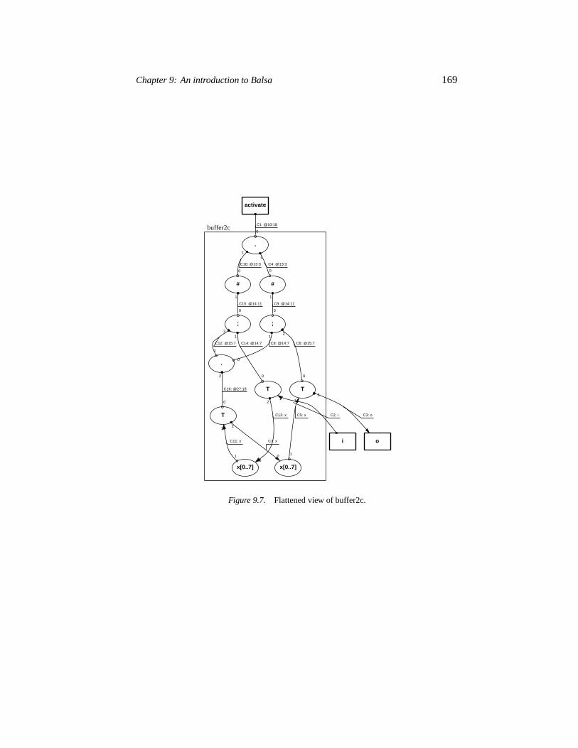
Chapter 9: An introduction to Balsa 169
buffer2c
activate
.
C1: @10:18
0
i o
#
C10: @13:3
0
1
#
C4: @13:3
0
2
x[0..7]
;
C15: @14:11
0
1
T
C14: @14:7
0
1
.
C12: @15:7
1
2
C2: i
1
C13: x
0
2
T
C11: x
1
1
x[0..7]
C7: x
0
2
;
C9: @14:11
0
1
T
C6: @15:7
0
2
C8: @14:7
0
1
C3: o
2
C5: x
1
1
C16: @27:18
0
2
Figure 9.7. Flattened view of buffer2c.
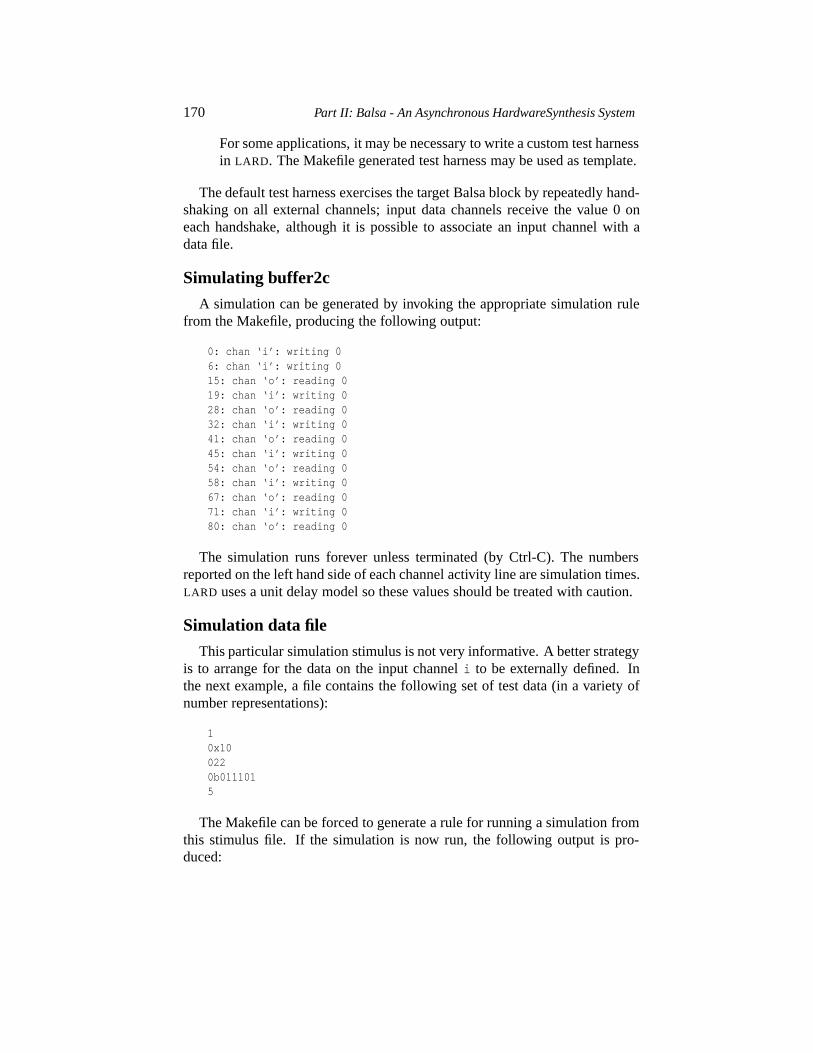
170 Part II: Balsa - An Asynchronous HardwareSynthesis System
For some applications, it may be necessary to write a custom test harnessin LARD. The Makefile generated test harness may be used as template.
The default test harness exercises the target Balsa block by repeatedly hand-shaking on all external channels; input data channels receive the value 0 oneach handshake, although it is possible to associate an input channel with adata file.
Simulating buffer2c
A simulation can be generated by invoking the appropriate simulation rulefrom the Makefile, producing the following output:
0: chan ‘i’: writing 06: chan ‘i’: writing 015: chan ‘o’: reading 019: chan ‘i’: writing 028: chan ‘o’: reading 032: chan ‘i’: writing 041: chan ‘o’: reading 045: chan ‘i’: writing 054: chan ‘o’: reading 058: chan ‘i’: writing 067: chan ‘o’: reading 071: chan ‘i’: writing 080: chan ‘o’: reading 0
The simulation runs forever unless terminated (by Ctrl-C). The numbersreported on the left hand side of each channel activity line are simulation times.LARD uses a unit delay model so these values should be treated with caution.
Simulation data file
This particular simulation stimulus is not very informative. A better strategyis to arrange for the data on the input channeli to be externally defined. Inthe next example, a file contains the following set of test data (in a variety ofnumber representations):
10x100220b0111015
The Makefile can be forced to generate a rule for running a simulation fromthis stimulus file. If the simulation is now run, the following output is pro-duced:
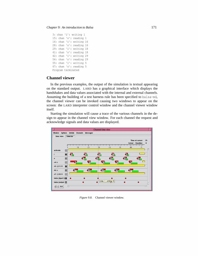
Chapter 9: An introduction to Balsa 171
3: chan ‘i’: writing 115: chan ‘o’: reading 116: chan ‘i’: writing 1628: chan ‘o’: reading 1629: chan ‘i’: writing 1841: chan ‘o’: reading 1842: chan ‘i’: writing 2954: chan ‘o’: reading 2955: chan ‘i’: writing 567: chan ‘o’: reading 5Program terminated
Channel viewer
In the previous examples, the output of the simulation is textual appearingon the standard output.LARD has a graphical interface which displays thehandshakes and data values associated with the internal and external channels.Assuming the building of a test harness rule has been specified tobalsa-md,the channel viewer can be invoked causing two windows to appear on thescreen: theLARD interpreter control window and the channel viewer windowitself.
Starting the simulation will cause a trace of the various channels in the de-sign to appear in the channel view window. For each channel the request andacknowledge signals and data values are displayed.
Figure 9.8. Channel viewer window.

Chapter 10
THE BALSA LANGUAGE
In this chapter, a tutorial overview of the language is given together withseveral small designs which illustrate various aspects of the language.
10.1. Data types
Balsa is strongly typed with data types based on bit vectors. The resultsof expressions must be guaranteed to fit within the range of the underlying bitvector representation. Types are either anonymous or named. Type equivalencefor anonymous types is checked on the basis of the size and properties of thetype, whereas type equivalence for named types is checked against the point ofdeclaration.
There are two classes of anonymous types: numeric types which are de-clared with thebits keyword, and arrays of other types. Numeric types canbe either signed or unsigned. Signedness has an effect on expression operatorsand casting. Only numeric types and arrays of other types may be used withoutfirst binding a name to those types. Balsa has three separate name spaces: onefor procedure and function names, a second for variable and channel namesand a third for type declarations.
Numeric types
Numeric types support the number range�0�2n�1� for n-bit unsigned num-bers or��2n�1�2n�1�1� for n-bit signed numbers. Named numeric types arejust aliases of the same range. An example of a numeric type declaration is:
type word is 16 bits
This defines a new typeword which is unsigned (there is no unsigned key-word) covering the range�0�216�1�. Alternatively, a signed type could havebeen declared as:
type sword is 16 signed bits
which defines a new typesword covering the range��215�215�1�.
173
174 Part II: Balsa - An Asynchronous HardwareSynthesis System
The only predefined type isbit. However the standard Balsa distributioncomes with with a set of library declarations for such types asbyte, nibble,boolean andcardinal as well as the constantstrue andfalse.
Enumerated types
Enumerated types consist of named numeric values. The named values aregiven values starting at zero and incrementing by one from left to right. Ele-ments with explicit values reset the counter and many names can be given tothe same value, for example:
type Colour is enumerationBlack, Brown, Red, Orange, Yellow, Green, Blue,Violet, Purple=Violet, Grey, Gray=Grey, White
end
The value of theViolet element ofColour is 7, as isPurple. BothGreyandGray have value 8. The total number of elements is 10. An enumerationcan be padded to a fixed size by use of theover keyword:
type SillyExample is enumeratione1=1, e2 over 4 bits
end
Here 2 bits are sufficient to specify the 3 possible values of the enumeration(0 is not bound to a name,e1 has the value 1 ande2 has the value 2). Theoverkeyword ensures that the representation of the enumerated type is actually 4bits. Enumerated types must be bound to names by a type declaration beforeuse.
Constants
Constant values can be defined in terms of an expression resolvable at com-pile time. Constants may be declared in terms of a predefined type otherwisethey default to a numeric type. Examples are:
constant minx = 5constant maxx = minx + 10constant hue = Red : Colourconstant colour = Colour’Green -- explicit enumeration element
Record types
Records are bit-wise compositions of named elements of possibly different(pre-declared) types with the first element occupying the least significant bitpositions, e.g.:
type Resistor is record
Chapter 10: The Balsa language 175
FirstBand, SecondBand, Multiplier : Colour;Tolerance : ToleranceColour
end
Resistor has four elements:FirstBand, SecondBand, Multiplier oftypeColour andTolerance of typeToleranceColour (both types must havebeen declared previously).FirstBand is the first element and so represents theleast significant portion of the bit-wise value of a typeResistor. Selection ofelements within the record structure is accomplished with the usual dot nota-tion. Thus ifR15 is a variable of typeResistor, the value of itsSecondBandcan extracted byR15.SecondBand. As with enumerations, record types can bepadded using theover notation.
Array types
Arrays are numerically indexed compositions of same-typed values. Anexample of the declaration of an array type is:
type RegBank_t : array 0..7 of byte
This introduces a new typeRegBank t which is an array type of 8 elementsindexed across the range [0, 7], each element being of typebyte. The orderingof the range specifier is irrelevant;array 0..7 is equivalent toarray 7..0.In general a single expression,expr, can be used to specify the array size: thisis equivalent to a range of0..expr-1. Anonymous array types are allowed inBalsa, so that variables can be declared as an array without first defining thearray type:
variable RegBank : array 0..7 of byte
Arbitrary ranges of elements within an array can be accessed by an arrayslicing mechanism e.g.a[5..7] extracts elementsa5, a6, anda7. As with allrange specifiers, the ordering of the range is irrelevant. In general Balsa packsall composite typed structures in a least significant to most significant, left toright manner. Array slices always return values which are based at index 0.
Arrays can be constructed by a tupling mechanism or by concatenation ofother arrays of the same base type:
variable a, b, c, d, e ,f: bytevariable z2 : array 2 of bytevariable z4 : array 4 of bytevariable z6 : array 6 of byte
z4:= {a,b,c,d} -- array constructionz6:= z4 @ {e, f} -- array concatenationz2:= (z4 @ {e, f}) [3..4] -- element extraction by array slicing
176 Part II: Balsa - An Asynchronous HardwareSynthesis System
In the last example, the first element ofz2 is set tod and the second elementis set toe. Array slicing is useful for extracting arbitrary bitfields from otherdatatypes.
Arrayed channels
Channels may be arrayed, that is they may consist of several distinct chan-nels which can be referred to by a numeric or enumerated index. This is similarto the way in which variables can have an array type except that each channelis distinct for the purposes of handshaking and each indexed channel has norelationship to the other channels in the array other than the single name theyshare. The syntax for arrayed channels is different from that of array typedvariables making it easier to disambiguate arrays from arrayed channels. Asan example:
array 4 of channel XYZ : array 4 of byte
declares 4 channels,XYZ[0] to XYZ[3], each channel is a 32-bit wide typearray 0..3 of byte. An example of the use of arrayed channels is shownin section 9.4.4 on page 165.
10.2. Data typing issues
As stated previously, Balsa is strongly typed: the left and right sides of as-signments are expected to have the same type. The only form of implicit type-casting is the promotion of numeric literals and constants to a wider numerictype. In particular, care must be taken to ensure that the result of an arithmeticoperation will always be compatible with the declared result type. Considerthe assignment statementx := x + 1. This is not a valid Balsa statement be-cause potentially the result is one bit wider than the width of the variablex. Ifthe carry-out from the addition is to be ignored, the user must explicitly forcethe truncation by means of a cast.
Casts
If the variablex was declared as 32 bits, the correct form of the assignmentabove is:
x := (x + 1 as 32 bits)
The keywordas indicates the cast operation. The parentheses are a neces-sary part of the syntax. If the carry out of the addition of two 32-bit numbersis required, a record type can be used to hold the composite result:
type AddResult is recordResult : 32 bits;
Chapter 10: The Balsa language 177
Carry : bit;endvariable r : AddResult
r := (a + b as AddResult)
The expressionr.Carry accesses the required carry bit,r.Result yieldsthe 32-bit addition result.
Casts are required when extracting bit fields. Here is an example from theinstruction decoder of a simple microprocessor. The bottom 5 bits of the 16-bitinstruction word contain an 5-bit signed immediate. It is required to extract theimmediate field and sign-extend it to 16 bits:
type Word is 16 signed bitstype Imm5 is 5 signed bits
variable Instr : 16 bits -- bottom 5 bits contain an immediatevariable Imm16 : Word
Imm16 := (((Instr as array 16 of bit) [0..4] as Imm5) as Word)
First, the instruction word,Instr, is cast into an array of bits from whichan arbitrary sub-range can be extracted:
(Instr as array 16 of bit)
Next the bottom (least significant) 5 bits must be extracted:
(Instr as array 16 of bit) [0..4]
The extracted 5 bits must now be cast back into a 5-bit signed number:
((Instr as array 16 of bit) [0..4] as Imm5)
The 5-bit signed number is then signed extended to the 16-bit immediatevalue:
(((Instr as array 16 of bit) [0..4] as Imm5) as Word)
The double cast is required because a straightforward cast from5 bits tothe variableImm16 of typeWord would have merely zero filled the topmost bitpositions even thoughWord is a signed type. However, a cast from a signednumeric type to another (wider) signed numeric type will sign extend the nar-rower value into the width of the wider target type.
Extracting bits from a field is a fairly common operation in many hardwaredesigns. In general, the original datatype has to be cast into an array first beforebitfield extraction. Thesmash operator “#” provides a convenient shorthand forcasting an object into an array of bits. Thus the sign extension example aboveis more simply written:
((#Instr [0..4] as Imm5) as Word)
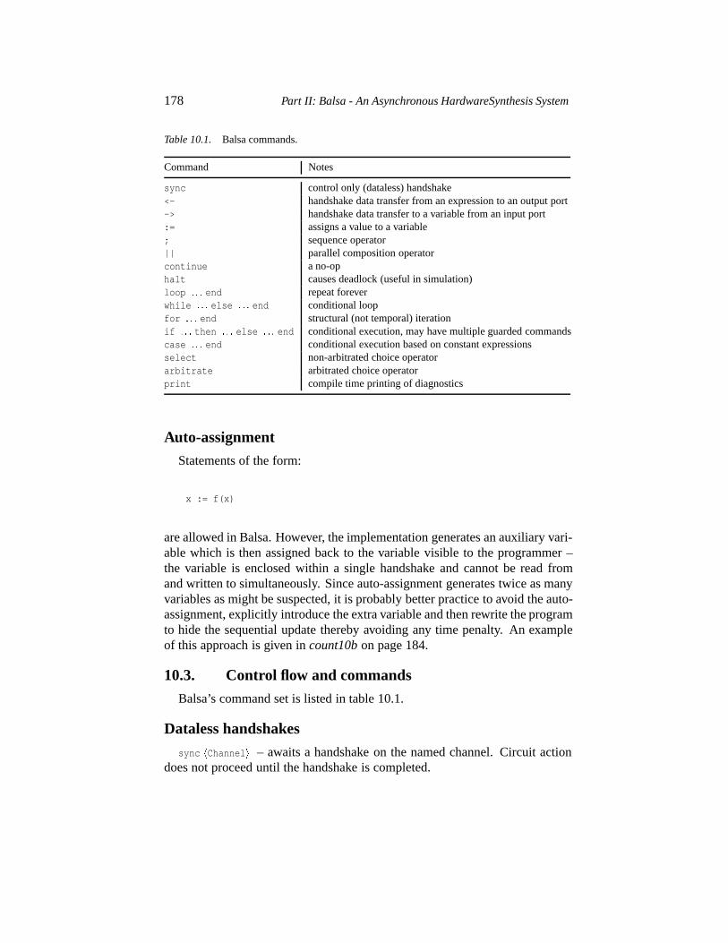
178 Part II: Balsa - An Asynchronous HardwareSynthesis System
Table 10.1. Balsa commands.
Command Notes
sync control only (dataless) handshake<- handshake data transfer from an expression to an output port-> handshake data transfer to a variable from an input port:= assigns a value to a variable; sequence operator|| parallel composition operatorcontinue a no-ophalt causes deadlock (useful in simulation)loop � � � end repeat foreverwhile � � � else � � � end conditional loopfor � � � end structural (not temporal) iterationif � � � then � � � else � � � end conditional execution, may have multiple guarded commandscase � � � end conditional execution based on constant expressionsselect non-arbitrated choice operatorarbitrate arbitrated choice operatorprint compile time printing of diagnostics
Auto-assignment
Statements of the form:
x := f(x)
are allowed in Balsa. However, the implementation generates an auxiliary vari-able which is then assigned back to the variable visible to the programmer –the variable is enclosed within a single handshake and cannot be read fromand written to simultaneously. Since auto-assignment generates twice as manyvariables as might be suspected, it is probably better practice to avoid the auto-assignment, explicitly introduce the extra variable and then rewrite the programto hide the sequential update thereby avoiding any time penalty. An exampleof this approach is given incount10b on page 184.
10.3. Control flow and commands
Balsa’s command set is listed in table 10.1.
Dataless handshakes
sync �Channel� – awaits a handshake on the named channel. Circuit actiondoes not proceed until the handshake is completed.
Chapter 10: The Balsa language 179
Channel communications
Data can be transferred between a variable and a channel, between channelsor from a channel to a command code block as shown below:
�Channel� <- �Variable� – transfers data from a variable to the named channel.This may either be an internal channel local to a procedure or an output portlisted in the procedure declaration.
�Channel� -> �Variable� – transfers data from the channel connected to avariable. The channel may either be an internal channel local to a procedure oran input port listed in the procedure declaration.
�Channel1� -> �Channel2� – transfers data between channels.
�Channel� -> then �Command� – allows the data to be accessed throughout thecommand block. However, the handshake on the channel is not completed andthus the data not released until the command block itself has terminated.
Variable assignment
�Variable� := �Expression� – transfers the result of an expression into a vari-able. The result type of the expression and that of the variable must agree.
Sequential composition
�Command1� ; �Command2� – the two commands execute sequentially. The firstmust terminate before the second commences.
Parallel composition
�Command1� || �Command2� – composes two commands such that they oper-ate concurrently and independently. Both commands must complete beforethe circuit action proceeds. Beware of inadvertently introducing dependenciesbetween the two commands so that neither can proceed until the other has com-pleted. The “||” operator binds tighter than “;”. If that is not what is intended,then commands may be grouped in blocks as shown below
[ �Command1� ; �Command2� ] || �Command3�
Note the use of square brackets to group commands rather than parentheses.Alternatively, the keywordsbegin � � � end may be used and are mandatory ifvariables local to a block are to be declared.
Continue and halt commands
continue is effectively a no-op. The commandhalt causes a processthread to deadlock.
180 Part II: Balsa - An Asynchronous HardwareSynthesis System
Looping constructs
Theloop command causes an infinite repetition of a block of code. Finiteloops may be constructed using thewhile construct. The simplest example ofits use is:
while �Condition� then �Command� end
However, multiple guards are allowed, so a more general form of the con-struct is:
while�Condition1� then �Command1�
| �Condition1� then �Command2�| �Condition3� then �Command3�else�Command4�
end
The ability of thewhile construct to take anelse clause is a minor conve-nience. The code sequence above could have been written, with only a smalldifference in the resultant handshake circuit implementation, as:
while�Condition1� then �Command1�
| �Condition2� then �Command2�| �Condition3� then �Command3�end;�Command4�
If more than one guard is satisfied, the particular command that is executedis unspecified.
Structural iteration
Balsa has a structural looping construct. In many programming languagesit is a matter of convenience or style as to whether a loop is written in terms ofa for loop or awhile loop. This is not so in Balsa. Thefor loop is similarto VHDL’s for � � � generate command and is used for iteratively laying outrepetitive structures. An example of its use was given earlier in section 9.4.4 onpage 165. An illustration of the inappropriate use of thefor command is givenin the examplecount10e on page 189. Structures may be iteratively instantiatedto operate either sequentially or concurrently with one another depending onwhetherfor ; or for || is employed.
Conditional execution
Balsa has two constructs to achieve conditional execution. Balsa’scasestatement is similar to that found in conventional programming languages. Asingle guard may match more than one value of the guard expression.
Chapter 10: The Balsa language 181
case x+y of1 .. 4, 11 then o <- x
| 5 .. 10 then o <- yelse o <- z
end
An if � � � then � � � else statement allows conditional execution based onthe evaluation of expressions at run-time. Its syntax is similar to that of thewhile loop. Note the sequencing implicit in nestedif statements, such as thatshown below:
if �Condition1� then�Command1�
elseif �Condition2� then�Command2�
endend
The test forCondition2 is made after the test forCondition1. If it isknown that the two conditions are mutually exclusive, the expression may bewritten:
if �Condition1� then �Command1�| �Condition2� then �Command2�end
The “|” separator causesCondition1 andCondition2 to be evaluated inparallel. The result is undefined if more than one guard (condition) is satisfied.
10.4. Binary/unary operators
Balsa’s binary/unary operators are shown in order of decreasing precedencein table 10.2.
10.5. Program structure
File structure
A typical design will consist of several files containing procedure/type/cons-tant declarations which come together in a top-level procedure that constitutesthe overall design. This top-level procedure would typically be at the end ofa file which imports all the other relevant design files. This importing featureforms a simple but effective way of allowing component reuse and maps sim-ply onto the notion of the imported procedures being either pre-compiled hand-shake circuits or existing (possibly hand crafted) library components. Declara-tions have a syntactically defined order (left to right, top to bottom) with eachdeclaration having its scope defined from the point of declaration to the end of
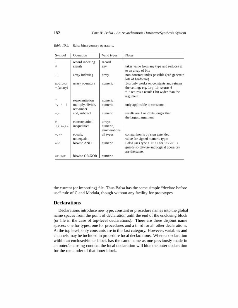
182 Part II: Balsa - An Asynchronous HardwareSynthesis System
Table 10.2. Balsa binary/unary operators.
Symbol Operation Valid types Notes
. record indexing record# smash any takes value from any type and reduces it
to an array of bits[] array indexing array non-constant index possible (can generate
lots of hardware)not,log, unary operators numeric log only works on constants and returns- (unary) the ceiling: e.g.log 15 returns 4
“-” returns a result 1 bit wider than theargument
ˆ exponentiation numeric*, /, % multiply, divide, numeric only applicable to constants
remainder+,- add, subtract numeric results are 1 or 2 bits longer than
the largest argument@ concatenation arrays<,>,<=,>= inequalities numeric,
enumerations=, /= equals, all types comparison is by sign extended
not equals value for signed numeric typesand bitwise AND numeric Balsa uses type1 bits for if/while
guards so bitwise and logical operatorsare the same.
or, xor bitwise OR,XOR numeric
the current (or importing) file. Thus Balsa has the same simple “declare beforeuse” rule of C and Modula, though without any facility for prototypes.
Declarations
Declarations introduce new type, constant or procedure names into the globalname spaces from the point of declaration until the end of the enclosing block(or file in the case of top-level declarations). There are three disjoint namespaces: one for types, one for procedures and a third for all other declarations.At the top level, only constants are in this last category. However, variables andchannels may be included in procedure local declarations. Where a declarationwithin an enclosed/inner block has the same name as one previously made inan outer/enclosing context, the local declaration will hide the outer declarationfor the remainder of that inner block.
Chapter 10: The Balsa language 183
Procedures
Procedures form the bulk of a Balsa description. Each procedure has a name,a set of ports and an accompanying behavioural description. Thesync key-word introduces dataless channels. Both dataless and data bearing channels canbe members of “arrayed channels”. Arrayed channels allow numeric/enumer-ated indexing of otherwise functionally separate channels. Procedures can alsocarry a list of local declarations which may include other procedures, types andconstants.
Shared procedures
Normally, each call to a procedure generates separate hardware to instan-tiate that procedure. A procedure may be shared, in which case calls to thatprocedure access common hardware thereby avoiding duplication of the cir-cuit at the cost of some multiplexing to allow sharing to occur. The use ofshared procedures is discussed further on page 187.
Functions
In many programming languages, functions can be thought of as procedureswithout side effects that return a result. However, in Balsa there is a fundamen-tal difference between functions and procedures. Parameters to a proceduredefine handshaking channels that interface to the circuit block defined by theprocedure. Function parameters, on the other hand, are just expression aliasesreturning values. An example of the use of function definitions can be foundin the arbiter tree design on page 202.
10.6. Example circuits
In this section, various designs of counter are described in Balsa. In flavour,they resemble the specifications of conventional synchronous counters, sincethese designs are more familiar to newcomers to asynchronous systems. Moresophisticated systolic counters, better suited to an asynchronous approach, aredescribed by van Berkel [14].
In this design, the role of the clock which updates the state of the counter istaken by a dataless sync channel, namedaclk. The counter issues a handshakerequest over the sync channel, the environment responds with an acknowledge-ment completing the handshake and the counter state is updated.
A modulo-16 counter-- count16a.balsa: modulo 16 counterimport [balsa.types.basic]
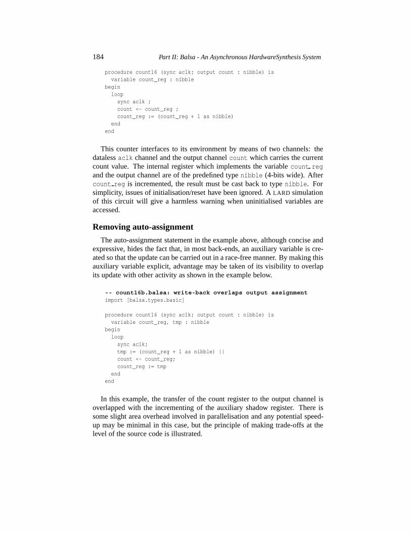
184 Part II: Balsa - An Asynchronous HardwareSynthesis System
procedure count16 (sync aclk; output count : nibble) isvariable count_reg : nibble
beginloopsync aclk ;count <- count_reg ;count_reg := (count_reg + 1 as nibble)
endend
This counter interfaces to its environment by means of two channels: thedatalessaclk channel and the output channelcount which carries the currentcount value. The internal register which implements the variablecount regand the output channel are of the predefined typenibble (4-bits wide). Aftercount reg is incremented, the result must be cast back to typenibble. Forsimplicity, issues of initialisation/reset have been ignored. ALARD simulationof this circuit will give a harmless warning when uninitialised variables areaccessed.
Removing auto-assignment
The auto-assignment statement in the example above, although concise andexpressive, hides the fact that, in most back-ends, an auxiliary variable is cre-ated so that the update can be carried out in a race-free manner. By making thisauxiliary variable explicit, advantage may be taken of its visibility to overlapits update with other activity as shown in the example below.
-- count16b.balsa: write-back overlaps output assignmentimport [balsa.types.basic]
procedure count16 (sync aclk; output count : nibble) isvariable count_reg, tmp : nibble
beginloopsync aclk;tmp := (count_reg + 1 as nibble) ||count <- count_reg;count_reg := tmp
endend
In this example, the transfer of the count register to the output channel isoverlapped with the incrementing of the auxiliary shadow register. There issome slight area overhead involved in parallelisation and any potential speed-up may be minimal in this case, but the principle of making trade-offs at thelevel of the source code is illustrated.
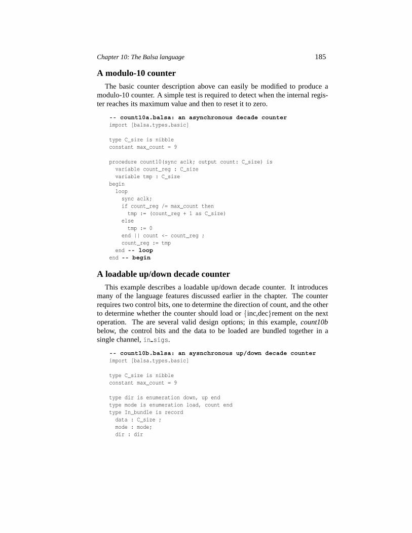
Chapter 10: The Balsa language 185
A modulo-10 counter
The basic counter description above can easily be modified to produce amodulo-10 counter. A simple test is required to detect when the internal regis-ter reaches its maximum value and then to reset it to zero.
-- count10a.balsa: an asynchronous decade counterimport [balsa.types.basic]
type C_size is nibbleconstant max_count = 9
procedure count10(sync aclk; output count: C_size) isvariable count_reg : C_sizevariable tmp : C_size
beginloop
sync aclk;if count_reg /= max_count thentmp := (count_reg + 1 as C_size)
elsetmp := 0
end || count <- count_reg ;count_reg := tmp
end -- loopend -- begin
A loadable up/down decade counter
This example describes a loadable up/down decade counter. It introducesmany of the language features discussed earlier in the chapter. The counterrequires two control bits, one to determine the direction of count, and the otherto determine whether the counter should load or�inc,dec�rement on the nextoperation. The are several valid design options; in this example,count10bbelow, the control bits and the data to be loaded are bundled together in asingle channel,in sigs.
-- count10b.balsa: an aysnchronous up/down decade counterimport [balsa.types.basic]
type C_size is nibbleconstant max_count = 9
type dir is enumeration down, up endtype mode is enumeration load, count endtype In_bundle is recorddata : C_size ;mode : mode;dir : dir
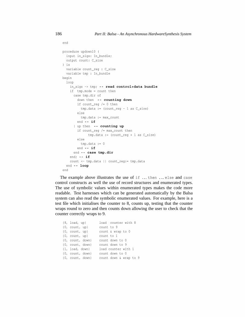
186 Part II: Balsa - An Asynchronous HardwareSynthesis System
end
procedure updown10 (input in_sigs: In_bundle;output count: C_size
) isvariable count_reg : C_sizevariable tmp : In_bundle
beginloopin_sigs -> tmp; -- read control+data bundleif tmp.mode = count thencase tmp.dir ofdown then -- counting downif count_reg /= 0 thentmp.data := (count_reg - 1 as C_size)
elsetmp.data := max_count
end -- if| up then -- counting upif count_reg /= max_count then
tmp.data := (count_reg + 1 as C_size)elsetmp.data := 0
end -- ifend -- case tmp.dir
end; -- ifcount <- tmp.data || count_reg:= tmp.data
end -- loopend
The example above illustrates the use ofif � � � then � � � else and casecontrol constructs as well the use of record structures and enumerated types.The use of symbolic values within enumerated types makes the code morereadable. Test harnesses which can be generated automatically by the Balsasystem can also read the symbolic enumerated values. For example, here is atest file which initialises the counter to 8, counts up, testing that the counterwraps round to zero and then counts down allowing the user to check that thecounter correctly wraps to 9.
{8, load, up} load counter with 8{0, count, up} count to 9{0, count, up} count & wrap to 0{0, count, up} count to 1{0, count, down} count down to 0{0, count, down} count down to 9{1, load, down} load counter with 1{0, count, down} count down to 0{0, count, down} count down & wrap to 9
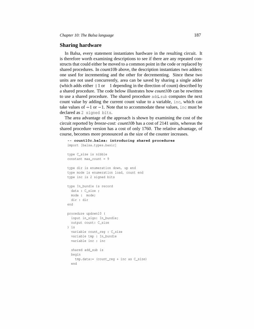
Chapter 10: The Balsa language 187
Sharing hardware
In Balsa, every statement instantiates hardware in the resulting circuit. Itis therefore worth examining descriptions to see if there are any repeated con-structs that could either be moved to a common point in the code or replaced byshared procedures. Incount10b above, the description instantiates two adders:one used for incrementing and the other for decrementing. Since these twounits are not used concurrently, area can be saved by sharing a single adder(which adds either�1 or�1 depending in the direction of count) described bya shared procedure. The code below illustrates howcount10b can be rewrittento use a shared procedure. The shared procedureadd sub computes the nextcount value by adding the current count value to a variable,inc, which cantake values of�1 or�1. Note that to accommodate these values,inc must bedeclared as2 signed bits.
The area advantage of the approach is shown by examining the cost of thecircuit reported bybreeze-cost: count10b has a cost of 2141 units, whereas theshared procedure version has a cost of only 1760. The relative advantage, ofcourse, becomes more pronounced as the size of the counter increases.
-- count10c.balsa: introducing shared proceduresimport [balsa.types.basic]
type C_size is nibbleconstant max_count = 9
type dir is enumeration down, up endtype mode is enumeration load, count endtype inc is 2 signed bits
type In_bundle is recorddata : C_size ;mode : mode;dir : dir
end
procedure updown10 (input in_sigs: In_bundle;output count: C_size
) isvariable count_reg : C_sizevariable tmp : In_bundlevariable inc : inc
shared add_sub isbegin
tmp.data:= (count_reg + inc as C_size)end
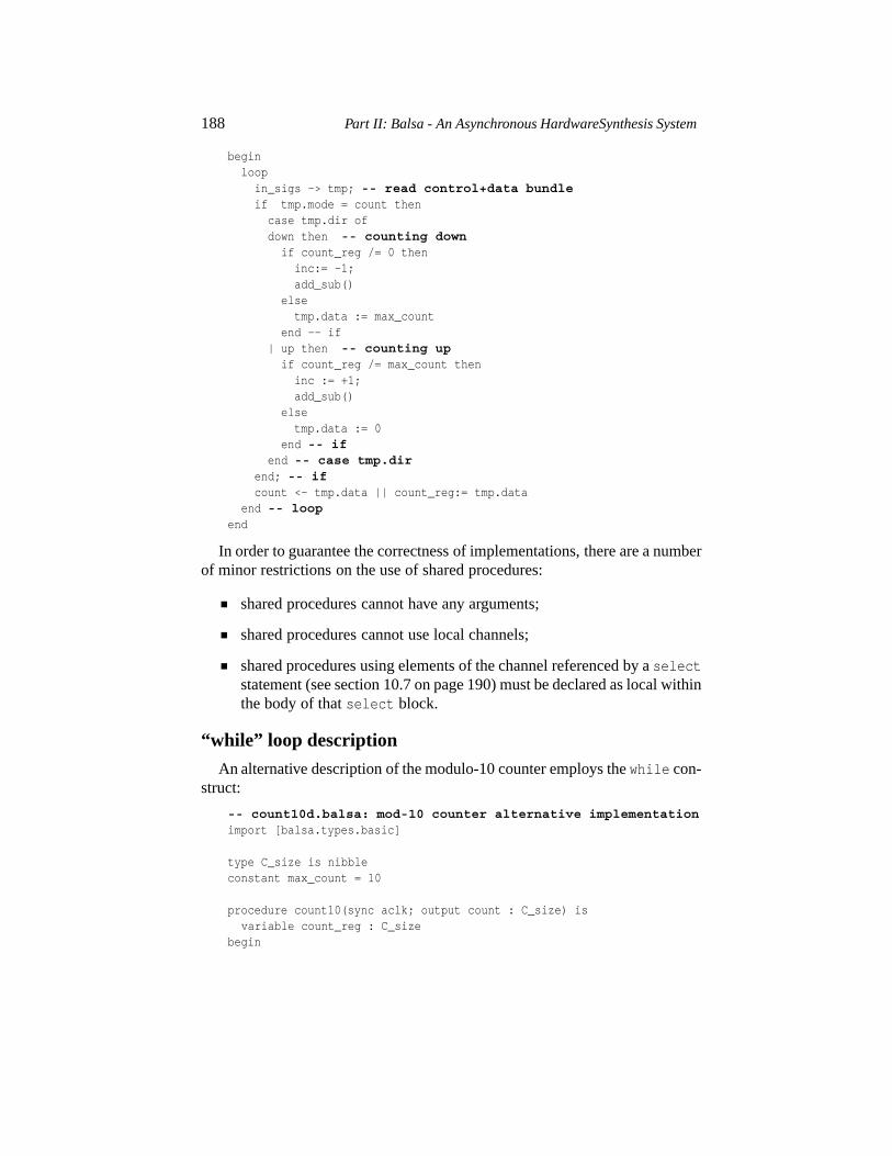
188 Part II: Balsa - An Asynchronous HardwareSynthesis System
beginloopin_sigs -> tmp; -- read control+data bundleif tmp.mode = count thencase tmp.dir ofdown then -- counting downif count_reg /= 0 theninc:= -1;add_sub()
elsetmp.data := max_count
end -- if| up then -- counting upif count_reg /= max_count theninc := +1;add_sub()
elsetmp.data := 0
end -- ifend -- case tmp.dir
end; -- ifcount <- tmp.data || count_reg:= tmp.data
end -- loopend
In order to guarantee the correctness of implementations, there are a numberof minor restrictions on the use of shared procedures:
shared procedures cannot have any arguments;
shared procedures cannot use local channels;
shared procedures using elements of the channel referenced by aselectstatement (see section 10.7 on page 190) must be declared as local withinthe body of thatselect block.
“while” loop description
An alternative description of the modulo-10 counter employs thewhile con-struct:
-- count10d.balsa: mod-10 counter alternative implementationimport [balsa.types.basic]
type C_size is nibbleconstant max_count = 10
procedure count10(sync aclk; output count : C_size) isvariable count_reg : C_size
begin
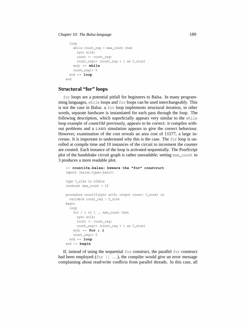
Chapter 10: The Balsa language 189
loopwhile count_reg < max_count thensync aclk;count <- count_reg;count_reg:= (count_reg + 1 as C_size)
end; -- whilecount_reg:= 0
end -- loopend
Structural “for” loops
for loops are a potential pitfall for beginners to Balsa. In many program-ming languages,while loops andfor loops can be used interchangeably. Thisis not the case in Balsa: afor loop implements structural iteration, in otherwords, separate hardware is instantiated for each pass through the loop. Thefollowing description, which superficially appears very similar to thewhileloop example ofcount10d previously, appears to be correct: it compiles with-out problems and aLARD simulation appears to give the correct behaviour.However, examination of the cost reveals an area cost of 11577, a large in-crease. It is important to understand why this is the case. Thefor loop is un-rolled at compile time and 10 instances of the circuit to increment the counterare created. Each instance of the loop is activated sequentially. The PostScriptplot of the handshake circuit graph is rather unreadable; settingmax_count to3 produces a more readable plot.
-- count10e.balsa: beware the "for" constructimport [balsa.types.basic]
type C_size is nibbleconstant max_count = 10
procedure count10(sync aclk; output count: C_size) isvariable count_reg : C_size
beginloop
for ; i in 1 .. max_count thensync aclk;count <- count_reg;count_reg:= (count_reg + 1 as C_size)
end; -- for ; icount_reg:= 0
end -- loopend -- begin
If, instead of using the sequentialfor construct, the parallelfor constructhad been employed (for || � � � ), the compiler would give an error messagecomplaining about read/write conflicts from parallel threads. In this case, all
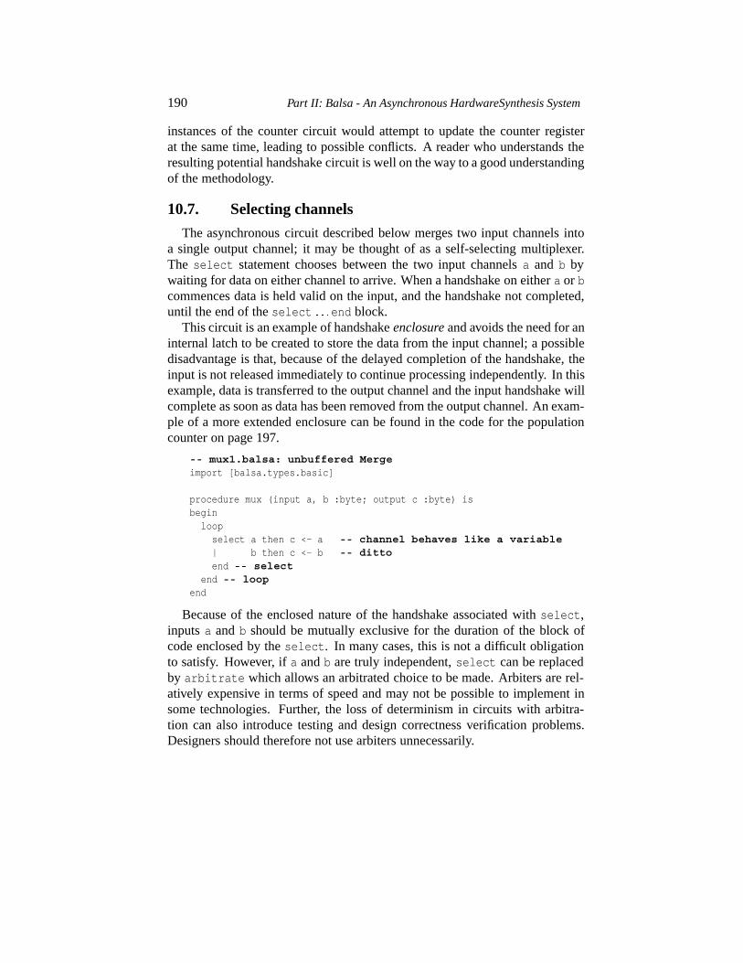
190 Part II: Balsa - An Asynchronous HardwareSynthesis System
instances of the counter circuit would attempt to update the counter registerat the same time, leading to possible conflicts. A reader who understands theresulting potential handshake circuit is well on the way to a good understandingof the methodology.
10.7. Selecting channels
The asynchronous circuit described below merges two input channels intoa single output channel; it may be thought of as a self-selecting multiplexer.The select statement chooses between the two input channelsa and b bywaiting for data on either channel to arrive. When a handshake on eithera or bcommences data is held valid on the input, and the handshake not completed,until the end of theselect � � �end block.
This circuit is an example of handshakeenclosure and avoids the need for aninternal latch to be created to store the data from the input channel; a possibledisadvantage is that, because of the delayed completion of the handshake, theinput is not released immediately to continue processing independently. In thisexample, data is transferred to the output channel and the input handshake willcomplete as soon as data has been removed from the output channel. An exam-ple of a more extended enclosure can be found in the code for the populationcounter on page 197.
-- mux1.balsa: unbuffered Mergeimport [balsa.types.basic]
procedure mux (input a, b :byte; output c :byte) isbegin
loopselect a then c <- a -- channel behaves like a variable| b then c <- b -- dittoend -- select
end -- loopend
Because of the enclosed nature of the handshake associated withselect,inputsa andb should be mutually exclusive for the duration of the block ofcode enclosed by theselect. In many cases, this is not a difficult obligationto satisfy. However, ifa andb are truly independent,select can be replacedby arbitrate which allows an arbitrated choice to be made. Arbiters are rel-atively expensive in terms of speed and may not be possible to implement insome technologies. Further, the loss of determinism in circuits with arbitra-tion can also introduce testing and design correctness verification problems.Designers should therefore not use arbiters unnecessarily.
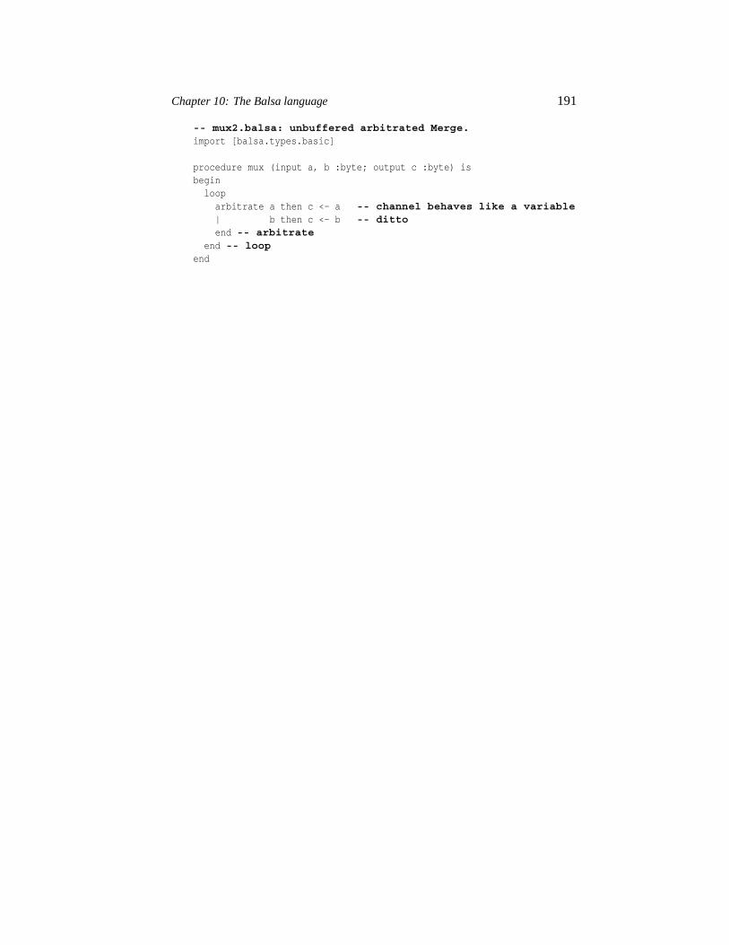
Chapter 10: The Balsa language 191
-- mux2.balsa: unbuffered arbitrated Merge.import [balsa.types.basic]
procedure mux (input a, b :byte; output c :byte) isbeginloop
arbitrate a then c <- a -- channel behaves like a variable| b then c <- b -- dittoend -- arbitrate
end -- loopend

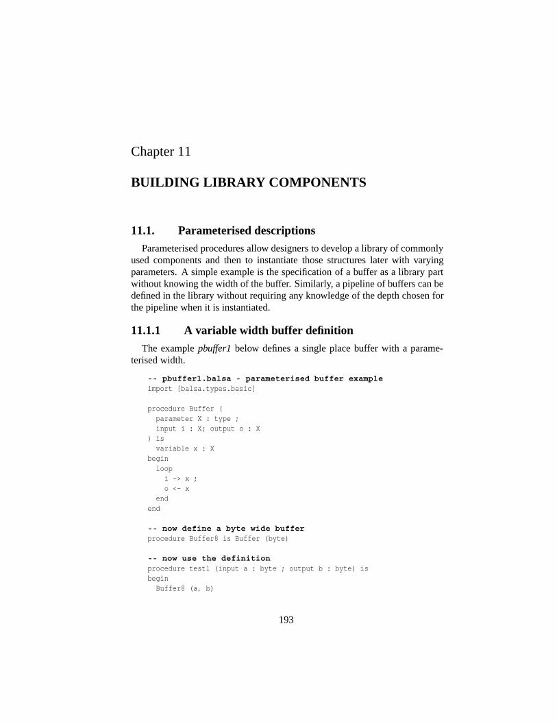
Chapter 11
BUILDING LIBRARY COMPONENTS
11.1. Parameterised descriptions
Parameterised procedures allow designers to develop a library of commonlyused components and then to instantiate those structures later with varyingparameters. A simple example is the specification of a buffer as a library partwithout knowing the width of the buffer. Similarly, a pipeline of buffers can bedefined in the library without requiring any knowledge of the depth chosen forthe pipeline when it is instantiated.
11.1.1 A variable width buffer definition
The examplepbuffer1 below defines a single place buffer with a parame-terised width.
-- pbuffer1.balsa - parameterised buffer exampleimport [balsa.types.basic]
procedure Buffer (parameter X : type ;input i : X; output o : X
) isvariable x : X
beginloop
i -> x ;o <- x
endend
-- now define a byte wide bufferprocedure Buffer8 is Buffer (byte)
-- now use the definitionprocedure test1 (input a : byte ; output b : byte) isbeginBuffer8 (a, b)
193
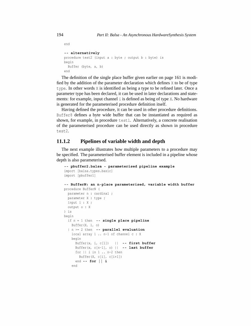
194 Part II: Balsa - An Asynchronous HardwareSynthesis System
end
-- alternativelyprocedure test2 (input a : byte ; output b : byte) isbegin
Buffer (byte, a, b)end
The definition of the single place buffer given earlier on page 161 is modi-fied by the addition of the parameter declaration which definesX to be of typetype. In other wordsX is identified as being a type to be refined later. Once aparameter type has been declared, it can be used in later declarations and state-ments: for example, input channeli is defined as being of typeX. No hardwareis generated for the parameterised procedure definition itself.
Having defined the procedure, it can be used in other procedure definitions.Buffer8 defines a byte wide buffer that can be instantiated as required asshown, for example, in proceduretest1. Alternatively, a concrete realisationof the parameterised procedure can be used directly as shown in proceduretest2.
11.1.2 Pipelines of variable width and depth
The next example illustrates how multiple parameters to a procedure maybe specified. The parameterised buffer element is included in a pipeline whosedepth is also parameterised.
-- pbuffer2.balsa - parameterised pipeline exampleimport [balsa.types.basic]import [pbuffer1]
-- BufferN: an n-place parameterised, variable width bufferprocedure BufferN (
parameter n : cardinal ;parameter X : type ;input i : X ;output o : X
) isbegin
if n = 1 then -- single place pipelineBuffer(X, i, o)
| n >= 2 then -- parallel evaluationlocal array 1 .. n-1 of channel c : XbeginBuffer(x, i, c[1]) || -- first bufferBuffer(x, c[n-1], o) || -- last bufferfor || i in 1 .. n-2 thenBuffer(X, c[i], c[i+1])
end -- for || iend

Chapter 11: Building library components 195
else print error, "zero length pipeline specified"end -- if
end
-- Now define a 4 deep, byte-wide pipeline.procedure Buffer4 is BufferN(4, byte)
Buffer is the single place parameterised width buffer of the previous exam-ple and this is reused by means of the library statementimport[pbuffer1].In this code,BufferN is defined in a very similar manner to the example in sec-tion 9.4.4 on page 165 except that the number of stages in the pipeline,n, isnot a constant but is a parameter to the definition of type cardinal. Note thatthis definition includes some error checking. If an attempt is made to build azero length pipeline during a definition, an error message is printed.
11.2. Recursive definitions
Balsa allows a form of recursion in definitions (as long as the resulting struc-tures can be statically determined at compile time). Many structures can bedescribed elegantly using this technique which forms a natural extension tothe powerful parameterisation mechanism. The remainder of this chapter il-lustrates recursive parameterisation by means of some interesting (and useful)examples.
11.2.1 An n-way multiplexer
An n-way multiplexer can be constructed from a tree of 2-way multiplexers.A recursive definition suggests itself as the natural specification technique: ann-way multiplexer can be split into two n/2-way multiplexers connected byinternal channels to a 2-way multiplexer as shown in figure 11.1 on page 196.
--- Pmux1.balsa: A recursive parameterised MUX definitionimport [balsa.types.basic]
procedure PMux (parameter X : type;parameter n : cardinal;array n of input inp : X; -- note use of arrayed portoutput out : X
) isbeginif n = 0 then print error,"Parameter n should not be zero"| n = 1 then
loopselect inp[0] thenout <- inp[0]
end -- selectend -- loop
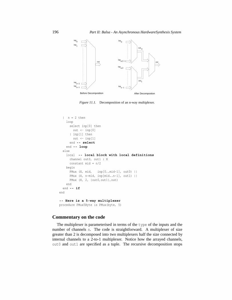
196 Part II: Balsa - An Asynchronous HardwareSynthesis System
0inp
n/2−1inp
n/2inp
n−1inp
0out
1out
out
After Decompostion
0inp
1inp
n−1inp
n−2inp
Before Decomposition
out
Figure 11.1. Decomposition of an n-way multiplexer.
| n = 2 thenloopselect inp[0] thenout <- inp[0]
| inp[1] thenout <- inp[1]
end -- selectend -- loop
elselocal -- local block with local definitionschannel out0, out1 : Xconstant mid = n/2
beginPMux (X, mid, inp[0..mid-1], out0) ||PMux (X, n-mid, inp[mid..n-1], out1) ||PMux (X, 2, {out0,out1},out)
endend -- if
end
-- Here is a 5-way multiplexerprocedure PMux5Byte is PMux(byte, 5)
Commentary on the code
The multiplexer is parameterised in terms of thetype of the inputs and thenumber of channelsn. The code is straightforward. A multiplexer of sizegreater than 2 is decomposed into two multiplexers half the size connected byinternal channels to a 2-to-1 multiplexer. Notice how the arrayed channels,out0 and out1 are specified as a tuple. The recursive decomposition stops
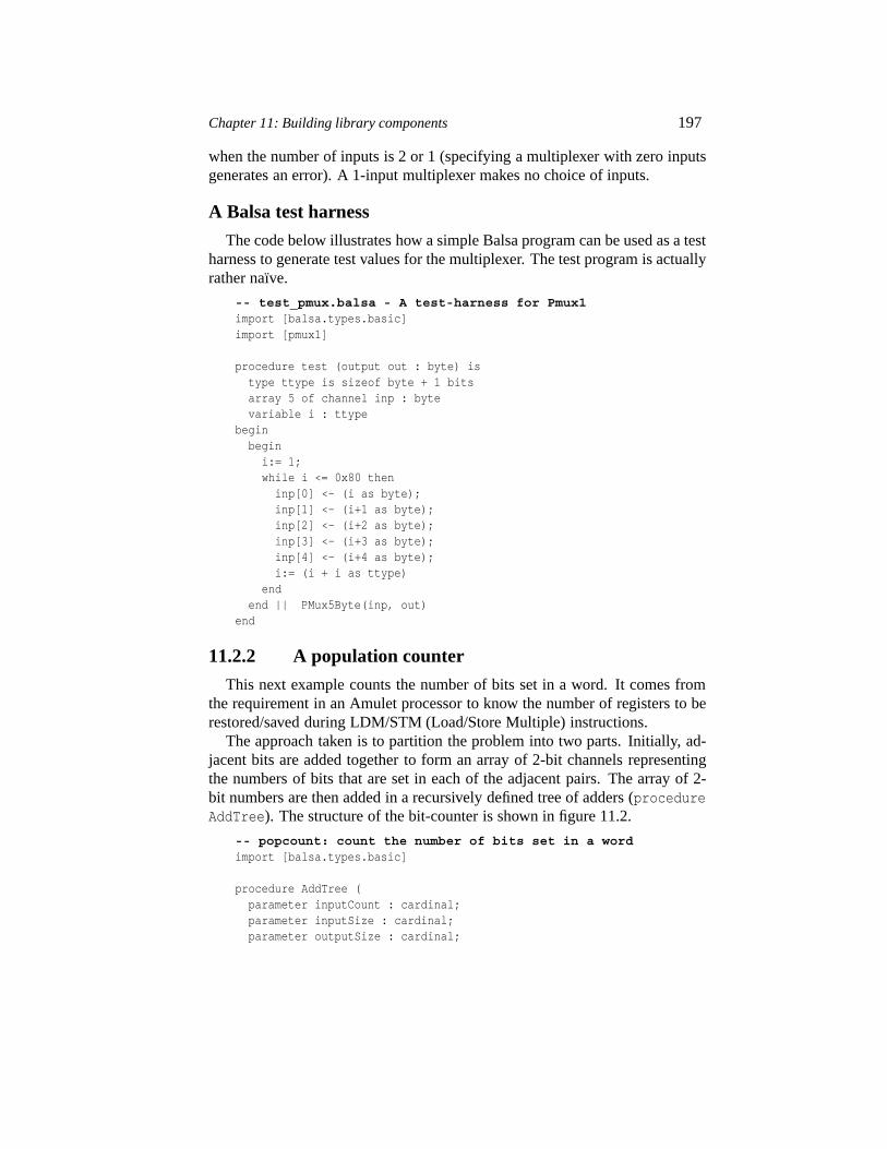
Chapter 11: Building library components 197
when the number of inputs is 2 or 1 (specifying a multiplexer with zero inputsgenerates an error). A 1-input multiplexer makes no choice of inputs.
A Balsa test harness
The code below illustrates how a simple Balsa program can be used as a testharness to generate test values for the multiplexer. The test program is actuallyrather na¨ıve.
-- test_pmux.balsa - A test-harness for Pmux1import [balsa.types.basic]import [pmux1]
procedure test (output out : byte) istype ttype is sizeof byte + 1 bitsarray 5 of channel inp : bytevariable i : ttype
beginbegin
i:= 1;while i <= 0x80 theninp[0] <- (i as byte);inp[1] <- (i+1 as byte);inp[2] <- (i+2 as byte);inp[3] <- (i+3 as byte);inp[4] <- (i+4 as byte);i:= (i + i as ttype)
endend || PMux5Byte(inp, out)
end
11.2.2 A population counter
This next example counts the number of bits set in a word. It comes fromthe requirement in an Amulet processor to know the number of registers to berestored/saved during LDM/STM (Load/Store Multiple) instructions.
The approach taken is to partition the problem into two parts. Initially, ad-jacent bits are added together to form an array of 2-bit channels representingthe numbers of bits that are set in each of the adjacent pairs. The array of 2-bit numbers are then added in a recursively defined tree of adders (procedureAddTree). The structure of the bit-counter is shown in figure 11.2.
-- popcount: count the number of bits set in a wordimport [balsa.types.basic]
procedure AddTree (parameter inputCount : cardinal;parameter inputSize : cardinal;parameter outputSize : cardinal;
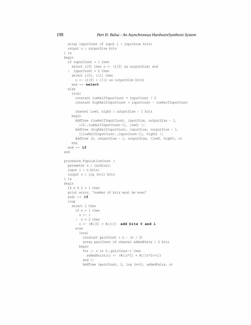
198 Part II: Balsa - An Asynchronous HardwareSynthesis System
array inputCount of input i : inputSize bits;output o : outputSize bits
) isbegin
if inputCount = 1 thenselect i[0] then o <- (i[0] as outputSize) end
| inputCount = 2 thenselect i[0], i[1] theno <- (i[0] + i[1] as outputSize bits)
end -- selectelselocalconstant lowHalfInputCount = inputCount / 2constant highHalfInputCount = inputCount - lowHalfInputCount
channel lowO, highO : outputSize - 1 bitsbeginAddTree (lowHalfInputCount, inputSize, outputSize - 1,i[0..lowHalfInputCount-1], lowO) ||
AddTree (highHalfInputCount, inputSize, outputSize - 1,i[lowHalfInputCount..inputCount-1], highO) ||
AddTree (2, outputSize - 1, outputSize, {lowO, highO}, o)end
end -- ifend
procedure PopulationCount (parameter n : cardinal;input i : n bits;output o : log (n+1) bits
) isbegin
if n % 2 = 1 thenprint error, "number of bits must be even"end; -- ifloopselect i thenif n = 1 theno <- i
| n = 2 theno <- (#i[0] + #i[1]) add bits 0 and 1
elselocalconstant pairCount = n - (n / 2)array pairCount of channel addedPairs : 2 bits
beginfor || c in 0..pairCount-1 then
addedPairs[c] <- (#i[c*2] + #i[(c*2)+1])end ||AddTree (pairCount, 2, log (n+1), addedPairs, o)
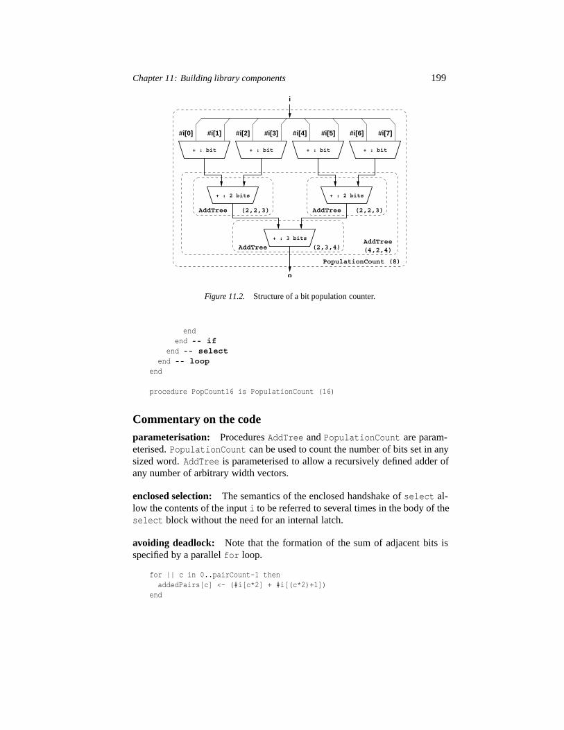
Chapter 11: Building library components 199
#i[0] #i[1] #i[2] #i[3] #i[4] #i[5] #i[6] #i[7]
+ : 2 bits + : 2 bits
+ : 3 bits
+ : bit + : bit + : bit+ : bit
o
PopulationCount (8)
(4,2,4)AddTree
(2,3,4)AddTree
i
(2,2,3)AddTree (2,2,3)AddTree
Figure 11.2. Structure of a bit population counter.
endend -- if
end -- selectend -- loop
end
procedure PopCount16 is PopulationCount (16)
Commentary on the code
parameterisation: ProceduresAddTree andPopulationCount are param-eterised.PopulationCount can be used to count the number of bits set in anysized word.AddTree is parameterised to allow a recursively defined adder ofany number of arbitrary width vectors.
enclosed selection: The semantics of the enclosed handshake ofselect al-low the contents of the inputi to be referred to several times in the body of theselect block without the need for an internal latch.
avoiding deadlock: Note that the formation of the sum of adjacent bits isspecified by a parallelfor loop.
for || c in 0..pairCount-1 thenaddedPairs[c] <- (#i[c*2] + #i[(c*2)+1])
end
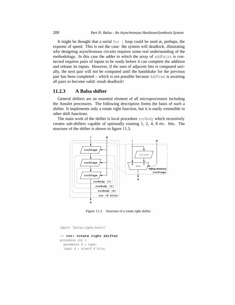
200 Part II: Balsa - An Asynchronous HardwareSynthesis System
It might be thought that a serialfor ; loop could be used at, perhaps, theexpense of speed. This isnot the case: the system will deadlock, illustratingwhy designing asynchronous circuits requires some real understanding of themethodology. In this case the adder to which the array ofaddPairs is con-nected requires pairs of inputs to be ready before it can complete the additionand release its inputs. However, if the sum of adjacent bits is computed seri-ally, the next pair will not be computed until the handshake for the previouspair has been completed – which is not possible becauseAddTree is awaitingall pairs to become valid: result deadlock!
11.2.3 A Balsa shifter
General shifters are an essential element of all microprocessors includingthe Amulet processors. The following description forms the basis of such ashifter. It implements only a rotate right function, but it is easily extensible toother shift functions.
The main work of the shifter is local procedurerorBody which recursivelycreates sub-shifters capable of optionally rotating 1, 2, 4, 8 etc. bits. Thestructure of the shifter is shown in figure 11.3.
rorStage
rorStage
rorStage
mux
rotate
#d[log distance]
i d
o
rorStage
0 1
rorBody (1)
rorBody (2)
rorBody (4)
i
o
ror (8 bits)
d
Figure 11.3. Structure of a rotate right shifter.
import [balsa.types.basic]
-- ror: rotate right shifterprocedure ror (
parameter X : type;input d : sizeof X bits;
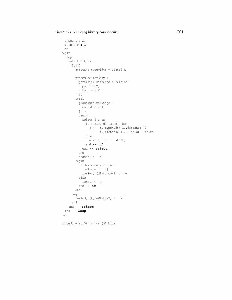
Chapter 11: Building library components 201
input i : X;output o : X
) isbeginloop
select d thenlocalconstant typeWidth = sizeof X
procedure rorBody (parameter distance : cardinal;input i : X;output o : X
) islocalprocedure rorStage (output o : X
) isbeginselect i then
if #d[log distance] theno <- (#i[typeWidth-1..distance] @
#i[distance-1..0] as X) {shift}elseo <- i {don’t shift}
end -- ifend -- select
endchannel c : X
beginif distance > 1 thenrorStage (c) ||rorBody (distance/2, c, o)
elserorStage (o)
end -- ifend
beginrorBody (typeWidth/2, i, o)
endend -- select
end -- loopend
procedure ror32 is ror (32 bits)
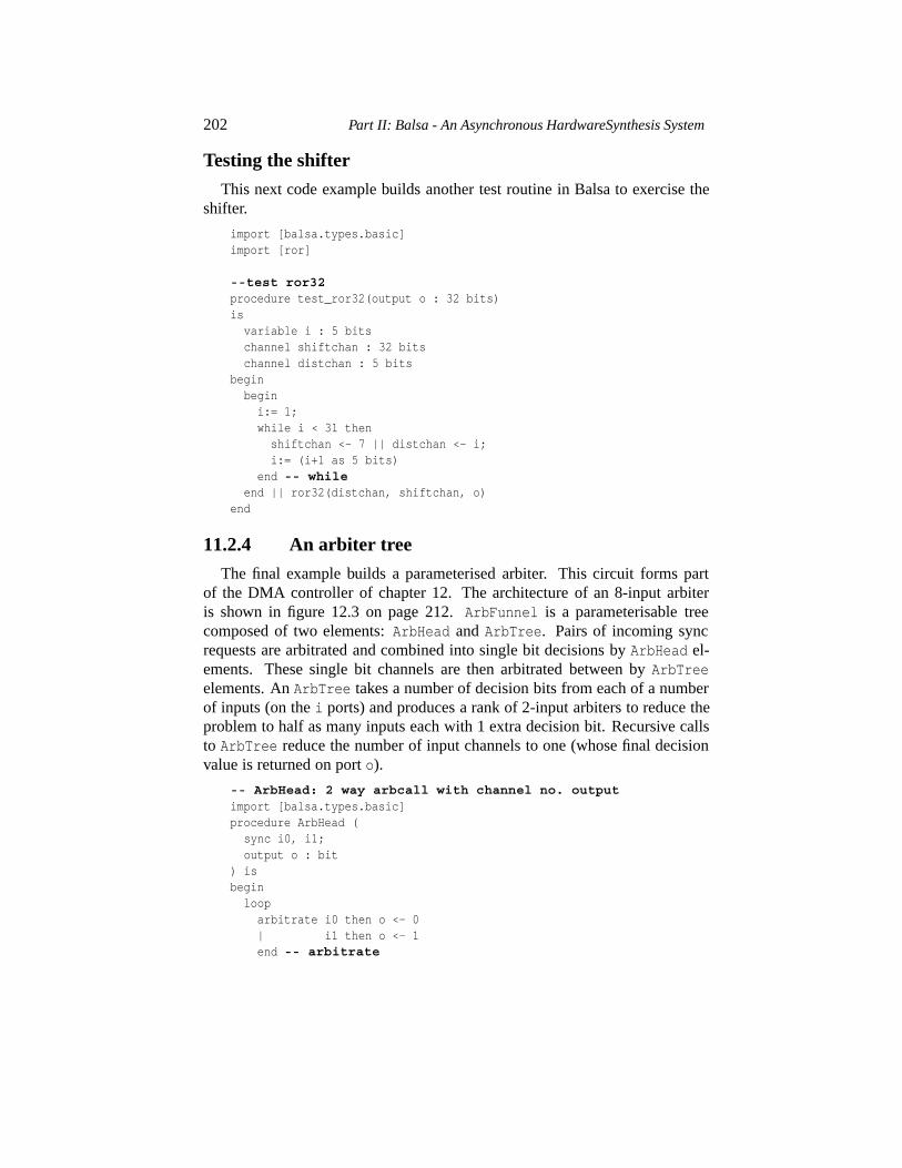
202 Part II: Balsa - An Asynchronous HardwareSynthesis System
Testing the shifter
This next code example builds another test routine in Balsa to exercise theshifter.
import [balsa.types.basic]import [ror]
--test ror32procedure test_ror32(output o : 32 bits)is
variable i : 5 bitschannel shiftchan : 32 bitschannel distchan : 5 bits
beginbegini:= 1;while i < 31 thenshiftchan <- 7 || distchan <- i;i:= (i+1 as 5 bits)
end -- whileend || ror32(distchan, shiftchan, o)
end
11.2.4 An arbiter tree
The final example builds a parameterised arbiter. This circuit forms partof the DMA controller of chapter 12. The architecture of an 8-input arbiteris shown in figure 12.3 on page 212.ArbFunnel is a parameterisable treecomposed of two elements:ArbHead andArbTree. Pairs of incoming syncrequests are arbitrated and combined into single bit decisions byArbHead el-ements. These single bit channels are then arbitrated between byArbTreeelements. AnArbTree takes a number of decision bits from each of a numberof inputs (on thei ports) and produces a rank of 2-input arbiters to reduce theproblem to half as many inputs each with 1 extra decision bit. Recursive callsto ArbTree reduce the number of input channels to one (whose final decisionvalue is returned on porto).
-- ArbHead: 2 way arbcall with channel no. outputimport [balsa.types.basic]procedure ArbHead (
sync i0, i1;output o : bit
) isbegin
looparbitrate i0 then o <- 0| i1 then o <- 1end -- arbitrate
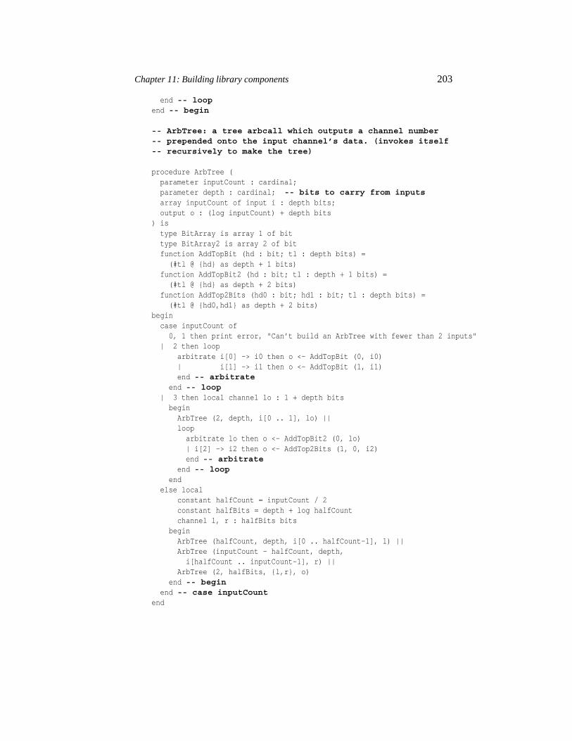
Chapter 11: Building library components 203
end -- loopend -- begin
-- ArbTree: a tree arbcall which outputs a channel number-- prepended onto the input channel’s data. (invokes itself-- recursively to make the tree)
procedure ArbTree (parameter inputCount : cardinal;parameter depth : cardinal; -- bits to carry from inputsarray inputCount of input i : depth bits;output o : (log inputCount) + depth bits
) istype BitArray is array 1 of bittype BitArray2 is array 2 of bitfunction AddTopBit (hd : bit; tl : depth bits) =
(#tl @ {hd} as depth + 1 bits)function AddTopBit2 (hd : bit; tl : depth + 1 bits) =
(#tl @ {hd} as depth + 2 bits)function AddTop2Bits (hd0 : bit; hd1 : bit; tl : depth bits) =
(#tl @ {hd0,hd1} as depth + 2 bits)begincase inputCount of
0, 1 then print error, "Can’t build an ArbTree with fewer than 2 inputs"| 2 then loop
arbitrate i[0] -> i0 then o <- AddTopBit (0, i0)| i[1] -> i1 then o <- AddTopBit (1, i1)end -- arbitrate
end -- loop| 3 then local channel lo : 1 + depth bits
beginArbTree (2, depth, i[0 .. 1], lo) ||looparbitrate lo then o <- AddTopBit2 (0, lo)| i[2] -> i2 then o <- AddTop2Bits (1, 0, i2)end -- arbitrate
end -- loopend
else localconstant halfCount = inputCount / 2constant halfBits = depth + log halfCountchannel l, r : halfBits bits
beginArbTree (halfCount, depth, i[0 .. halfCount-1], l) ||ArbTree (inputCount - halfCount, depth,i[halfCount .. inputCount-1], r) ||
ArbTree (2, halfBits, {l,r}, o)end -- begin
end -- case inputCountend
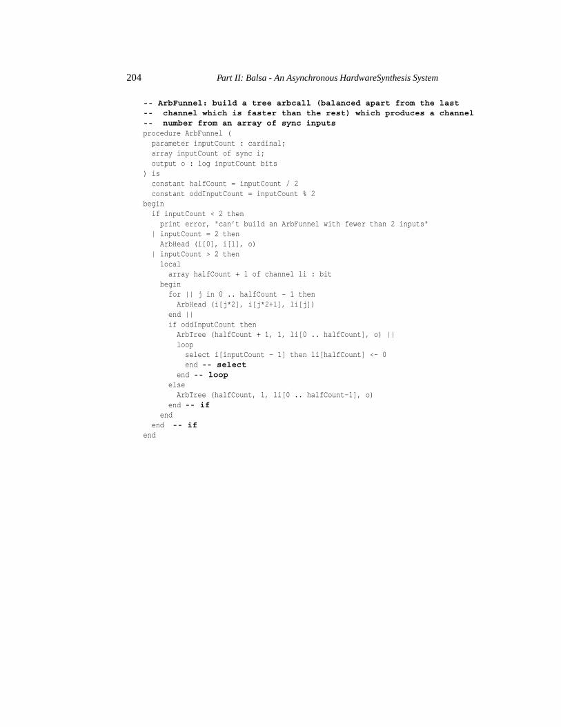
204 Part II: Balsa - An Asynchronous HardwareSynthesis System
-- ArbFunnel: build a tree arbcall (balanced apart from the last-- channel which is faster than the rest) which produces a channel-- number from an array of sync inputsprocedure ArbFunnel (
parameter inputCount : cardinal;array inputCount of sync i;output o : log inputCount bits
) isconstant halfCount = inputCount / 2constant oddInputCount = inputCount % 2
beginif inputCount < 2 thenprint error, "can’t build an ArbFunnel with fewer than 2 inputs"
| inputCount = 2 thenArbHead (i[0], i[1], o)
| inputCount > 2 thenlocalarray halfCount + 1 of channel li : bit
beginfor || j in 0 .. halfCount - 1 thenArbHead (i[j*2], i[j*2+1], li[j])
end ||if oddInputCount thenArbTree (halfCount + 1, 1, li[0 .. halfCount], o) ||loopselect i[inputCount - 1] then li[halfCount] <- 0end -- select
end -- loopelseArbTree (halfCount, 1, li[0 .. halfCount-1], o)
end -- ifend
end -- ifend
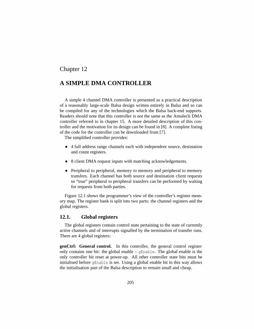
Chapter 12
A SIMPLE DMA CONTROLLER
A simple 4 channel DMA controller is presented as a practical descriptionof a reasonably large-scale Balsa design written entirely in Balsa and so canbe compiled for any of the technologies which the Balsa back-end supports.Readers should note that this controller is not the same as the Amulet3i DMAcontroller referred to in chapter 15. A more detailed description of this con-troller and the motivation for its design can be found in [8]. A complete listingof the code for the controller can be downloaded from [7].
The simplified controller provides:
4 full address range channels each with independent source, destinationand count registers.
8 client DMA request inputs with matching acknowledgements.
Peripheral to peripheral, memory to memory and peripheral to memorytransfers. Each channel has both source and destination client requestsso “true” peripheral to peripheral transfers can be performed by waitingfor requests from both parties.
Figure 12.1 shows the programmer’s view of the controller’s register mem-ory map. The register bank is split into two parts: the channel registers and theglobal registers.
12.1. Global registers
The global registers contain control state pertaining to the state of currentlyactive channels and of interrupts signalled by the termination of transfer runs.There are 4 global registers:
genCtrl: General control. In this controller, the general control registeronly contains one bit: the global enable –gEnable. The global enable is theonly controller bit reset at power-up. All other controller state bits must beinitialised beforegEnable is set. Using a global enable bit in this way allowsthe initialisation part of the Balsa description to remain small and cheap.
205
206 Part II: Balsa - An Asynchronous HardwareSynthesis System
01234511:9 8:6
chan[n].ctrl
enablesrcInc
dstInccountDec
srcDRQdstDRQ
srcClientNodstClientNo
31 23 15 024 16 8 7
chan[0].src
chan[0].dst
chan[0].count
chan[1].dst
chan[1].count
chan[2].src
chan[2].count
chan[3].src
chan[3].count
chan[1].src
chan[2].dst
00000400800C
01001401801C
02002402802C
03003403803C
Reads as 0x0000 0...
Reads as 0x0000 0...
Reads as 0x0000 0...
Reads as 0x0000 0...
genCtrlReads as 0/1200
204
208
20C
chanStatus
IRQMask
IRQReq
Reads as 0x0000 000...
Reads as 0x0000 000...
Reads as 0x0000 000...
chan[0].ctrl
chan[2].ctrl
chan[3].ctrl
chan[2].dst
chan[1].ctrl
genCtrl.gEnable
global registers
channel registers
Figure 12.1. DMA controller programmer’s model.
chanStatus: Channel end-of-run status. ThechanStatus register contains4 bits, one per DMA channel. When set by the DMA controller, a bit in thisregister indicates that the corresponding channel has come to the end of its runof transfers.
IRQMask, IRQReq: Interrupt mask and status. The IRQMask registercontains one bit per channel (likechanStatus) with set bits specifying thatan interrupt should be raised at the end of a transfer run of that channel (whenthe correspondingchanStatus bit becomes set).IRQReq contains the currentinterrupt status for each channel.
The channel status, IRQ mask and IRQ status bits are kept in global registersin order to reduce the number of DMA register reads which must be performedby the CPU after receiving an interrupt in order to determine which channel toservice.
12.2. Channel registers
Each channel has 4 registers associated with it in the same way as theAmulet3i DMA controller. The two address registers (channel[n].src andchannel[n].dst) specify the 32-bit source and destination addresses for trans-fers. The count register (channel[n].count) is a 32-bit count of remaining
Chapter 12: A simple DMA controller 207
transfers to perform; transfer runs terminate when the count register is decre-mented to zero. The control register (channel[n].ctrl) specifies the updatesto be performed on the other three registers and the clients to which this chan-nel is connected. Writing to the control register has the effect of clearing inter-rupts and end-of-run indication on that channel. The control register contains8 fields:
enable: Transfer enable. If the enable bit is set, this channel should beconsidered for transfers when a new DMA request arrives. Channel enablesare not cleared on power-up. ThegenCtrl.gEnable bit can be used to pre-vent transfers from occurring whilst the channel enable bits are cleared duringstartup.
srcInc, dstInc, countDec: Increment/decrement control. These bits areused to enable source, destination and count register update after a transfer.Source and destination registers are incremented by 4 after transfers (sinceonly word transfers are supported in this version of the controller) ifsrcIncanddstInc (respectively) are set. Note that the bottom 2 bits of these ad-dresses are preserved. The count register is decremented by 1 after each trans-fer if countDec is set. Resetting eithersrcInc or dstInc results in the corre-sponding address remaining unchanged between transfers. This is useful fornominating peripheral (rather than memory) addresses. ResettingcountDecresults in “free-running” transfers.
srcDRQ, dstDRQ: Initial DMA requests. Transfers can take place on achannel when a pair of DMA requests have been received, one for the sourceclient and the other for the destination client (therequests-pending registers).ThesrcDRQ anddstDRQ bits specify the initial states for those two requests.Setting both of these bits indicates that the source and destination requestsshould be considered to have already arrived. Resetting one or both of the bitsspecifies that requests from the corresponding�src,dst�ClientNo numberedclient should trigger a transfer (both client requests are required when bothcontrol bits are reset).
srcClientNo, dstClientNo: Client to channel mapping. These fields spec-ify the client numbers from which this channel receives source and destinationDMA requests. These fields are only of use when eithersrcDRQ or dstDRQ (orboth) are reset.
12.3. DMA controller structure
The structure of the simplified DMA controller is shown in Figure 12.2. Thesimplified DMA controller is composed of 5 units:
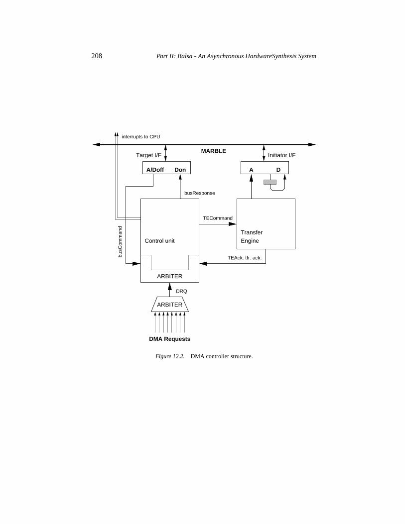
208 Part II: Balsa - An Asynchronous HardwareSynthesis System
ARBITER
DMA Requests
DRQ
MARBLE
TECommand
ARBITER
interrupts to CPU
A/Doff Don
busResponse
Control unit EngineTransfer
TEAck: tfr. ack.
A D
Initiator I/FTarget I/F
busC
omm
and
Figure 12.2. DMA controller structure.
Chapter 12: A simple DMA controller 209
MARBLE target interface
The controller is assumed to be attached to the MARBLE asynchronousbus which connects the subsystems in the Amulet3i system-on-chip (see chap-ter 15). It is relatively easy to provide an interface to other forms of on-chipsystem connect busses.
The MARBLE target interface provides a connection to MARBLE throughwhich the controller can be programmed. Accesses to the registers from thisinterface are arbitrated with incoming DMA requests andtransfer acknowl-edgements from the transfer engine. This arbitration and the decoupling oftransfer engine from control unit allow the DMA controller to avoid potentialbus access deadlock situations.
The MARBLE interface used here carries an 8-bit address (8-bit word ad-dress, 10-bit byte address) similar to that of the Amulet3i DMA controller.This allows the same address mapping of channel registers and the possibil-ity of extendeding the number of channels to 32 without changing the globalregister addresses.
MARBLE initiator interface
The initiator interface is used by the DMA controller to perform its transfers.Only the address and control bits to this interface are connected to the Balsasynthesised controller hardware. The data to and from the initiator interface ishandled by a latch (shown as the shaded box in Figure 12.2). Only word-widetransfers are supported and so this latch is all that is needed to hold data valuesbetween the read and write bus transactions of a transfer. Supporting differenttransfer widths is relatively easy but has not been implemented in this examplein order to simplify the code.
Control unit
Each DMA channel has a pair of register bits, therequests-pending bits,which recode the arrival of requests for that channel’s source and destinationclients. After marking-up an incoming request, the control unit examines therequests-pending registers of each channel in turn to find a channel on whichto perform a transfer. If a transfer is to be performed, the register contents forthat channel are forwarded to the transfer engine and the register contents areupdated to reflect the incremented addresses and decremented count. DMArequests are acknowledged straight away when no transfer engine commandis issued, or just after the command is issued where a transfer command isissued to the transfer engine. The acknowledgement of DMA requests doesnot guarantee the timely completion of the related transfer, peripherals mustobserve bus accesses made to themselves for this purpose. The acknowledge-
210 Part II: Balsa - An Asynchronous HardwareSynthesis System
ment serves only to confirm the receipt of the DMA transfer request. A requestmust be removed after an acknowledgement is signalled so that other requestscan be received through the request arbitration tree to mark-up potential trans-fers for other channels.
Transfer engine
The controller’s transfer engine takes commands from the control unit whena DMA transfer is due to be performed and performs no DMA request mappingor filtering of its own. The only reason for having the transfer engine is toprevent the potential bus deadlock situation if an access to the register bankis made across MARBLE while the DMA controller is trying to perform atransfer. In this situation, control of the bus belongs to the initiator (usuallythe CPU) trying to access the DMA controller. This initiator cannot proceedas the DMA controller is engaged in trying to gain the bus for itself. With atransfer engine, and the decoupling of DMA request/CPU access from transferoperations, the control unit is free to fulfil the initiator’s register request whilethe transfer engine is waiting for the bus to become available.
After performing a transfer, the transfer engine will signal to the controlunit to provide a new transfer command; it does this by a handshake on thetransfer acknowledge channel (markedTEAck in Figure 12.2). This channelpasses through the control unit’s command arbitration hardware and serves toinform the control unit that the transfer engine is free and that the request-pending register can be polled to find the next suitable transfer candidate. Theacknowledgement not only provides the self-looping activation required to per-form memory to memory transfers but also allows the looping required to ser-vice requests for other types of transfer which are received during the periodwhen the transfer engine was busy.
A flag register,TEBusy, held in the control unit, is used to record the statusof the transfer engine so that commands are not issued to it while a transferis in progress. This flag is set each time a transfer command is issued to thetransfer engine and cleared each time a transfer acknowledgement is receivedby the control unit. The request-pending registers are not re-examined (and atransfer command issued) ifTEBusy is set.
Arbiter tree
The DMA controller receives DMA requests on an array of 8 sync channelsconnected to the input of the ARBITER unit shown in Figure 12.2. This arbiterunit is a tree of 2-way arbiter cells that combines these 8 inputs into a singleDMA request number which it provides to the control unit. DMA requestsare acknowledged as soon as the control unit has recorded them. Only thesuccessful transfer of data between peripherals should be used as an indication
Chapter 12: A simple DMA controller 211
of the actual completion of a DMA operation. When a transfer is begun (i.e.passed from control unit to transfer engine), that transfer’s channel registersand requests-pending registers are updated before another arbitrated access tothe control unit is accepted. As a consequence, a new request on a channel canarrive (and be correctly observed) as soon as any transfer-related bus activityoccurs for that transfer.
12.4. The Balsa description
The Balsa description of the DMA controller is composed of 3 parts: thearbiter tree, the control unit and the transfer engine. The two MARBLE inter-faces sit outside the Balsa block and are controlled through the target (mta andmtd) ports (corresponding to command and response ports) and the initiatoraddress/control (mia) port. The top level of the DMA controller is:
procedure DMAArb is ArbFunnel (NoOfClients)
procedure dma (input mta : MARBLE8bACommand;output mtd : MARBLEResponse;output mia : MARBLECommandNoData;output irq : bit;array NoOfClients of sync drq
) ischannel DRQClientNo : ClientNochannel TECommand : array 2 of Word \textbf{--srcAddr, dstAddr}sync TEAck
beginDMAArb (drq, DRQClientNo) ||DMAControl (mta, mtd, DRQClientNo, TECommand, TEAck, IRQ) ||DMATransferEngine (TECommand, TEAck, mia)
end
Interrupts are signalled by writing a 0 or 1 to theirq port. This interruptvalue must then be caught by an external latch to generate a bare interruptsignal.
12.4.1 Arbiter tree
DMA requests from the client peripherals arrive on the sync channelsdrq,these channels connect to the request arbiterDMAArb. The procedure declara-tion for DMAArb is given in the top level as a parameterised version of the pro-cedureArbFunnel and was described in chapter 11 on page 202. Figure 12.3shows the organisation of an 8-inputArbFunnel.
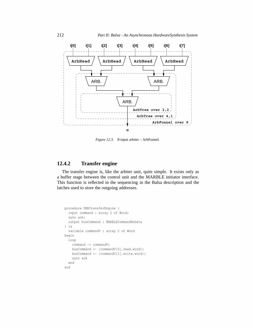
212 Part II: Balsa - An Asynchronous HardwareSynthesis System
ARB.
ARB.
ARB.
ArbHead ArbHead
ArbTree over 2,2
ArbTree over 4,1
ArbFunnel over 8
o
ArbHead ArbHead
i[0] i[1] i[2] i[3] i[4] i[5] i[6] i[7]
Figure 12.3. 8-input arbiter – ArbFunnel.
12.4.2 Transfer engine
The transfer engine is, like the arbiter unit, quite simple. It exists only asa buffer stage between the control unit and the MARBLE initiator interface.This function is reflected in the sequencing in the Balsa description and thelatches used to store the outgoing addresses.
procedure DMATransferEngine (input command : array 2 of Word;sync ack;output busCommand : MARBLECommandNoData
) isvariable commandV : array 2 of Word
beginloopcommand -> commandV;busCommand <- {commandV[0],read,word};busCommand <- {commandV[1],write,word};sync ack
endend
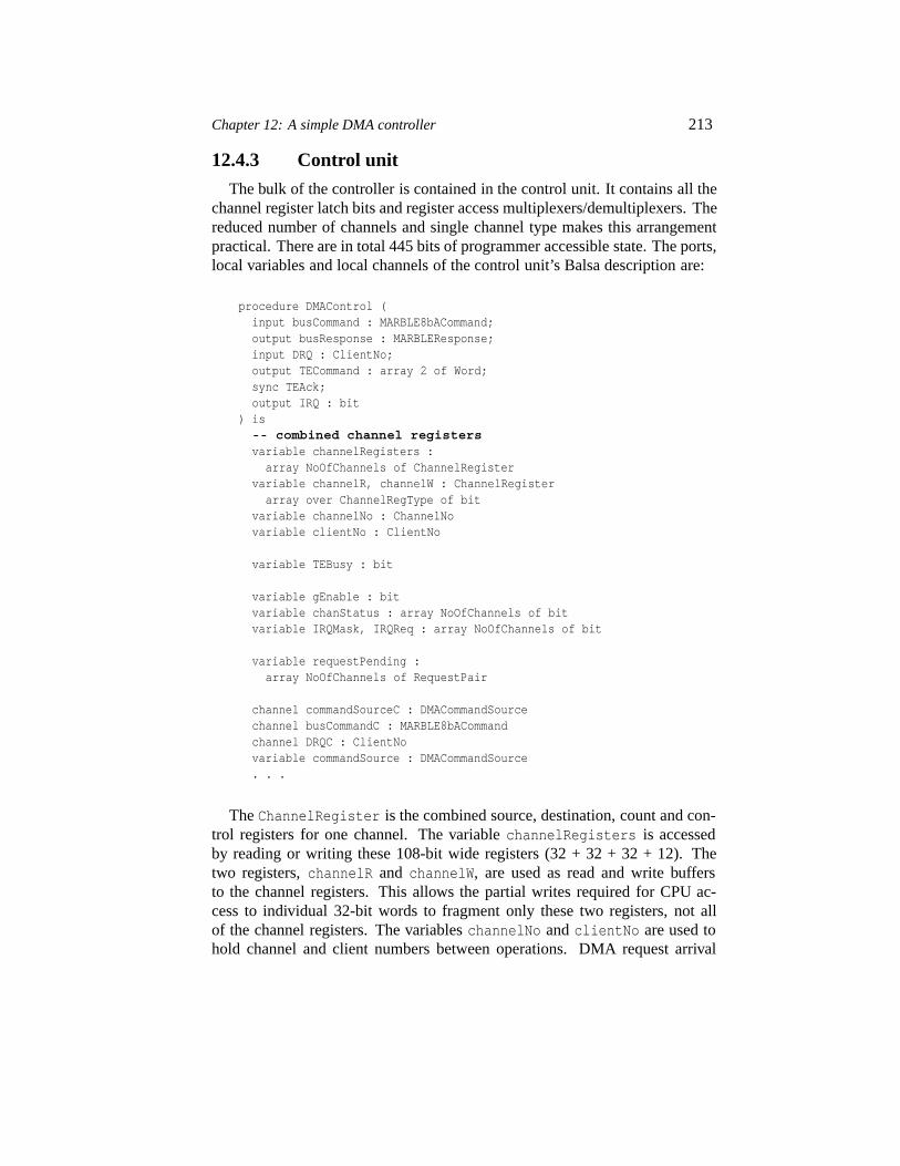
Chapter 12: A simple DMA controller 213
12.4.3 Control unit
The bulk of the controller is contained in the control unit. It contains all thechannel register latch bits and register access multiplexers/demultiplexers. Thereduced number of channels and single channel type makes this arrangementpractical. There are in total 445 bits of programmer accessible state. The ports,local variables and local channels of the control unit’s Balsa description are:
procedure DMAControl (input busCommand : MARBLE8bACommand;output busResponse : MARBLEResponse;input DRQ : ClientNo;output TECommand : array 2 of Word;sync TEAck;output IRQ : bit
) is-- combined channel registersvariable channelRegisters :
array NoOfChannels of ChannelRegistervariable channelR, channelW : ChannelRegister
array over ChannelRegType of bitvariable channelNo : ChannelNovariable clientNo : ClientNo
variable TEBusy : bit
variable gEnable : bitvariable chanStatus : array NoOfChannels of bitvariable IRQMask, IRQReq : array NoOfChannels of bit
variable requestPending :array NoOfChannels of RequestPair
channel commandSourceC : DMACommandSourcechannel busCommandC : MARBLE8bACommandchannel DRQC : ClientNovariable commandSource : DMACommandSource. . .
TheChannelRegister is the combined source, destination, count and con-trol registers for one channel. The variablechannelRegisters is accessedby reading or writing these 108-bit wide registers (32 + 32 + 32 + 12). Thetwo registers,channelR and channelW, are used as read and write buffersto the channel registers. This allows the partial writes required for CPU ac-cess to individual 32-bit words to fragment only these two registers, not allof the channel registers. The variableschannelNo andclientNo are used tohold channel and client numbers between operations. DMA request arrival
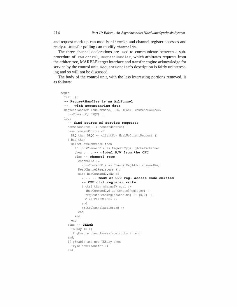
214 Part II: Balsa - An Asynchronous HardwareSynthesis System
and request mark-up can modifyclientNo and channel register accesses andready-to-transfer polling can modifychannelNo.
The three channel declarations are used to communicate between a sub-procedure ofDMAControl, RequestHandler, which arbitrates requests fromthe arbiter tree, MARBLE target interface and transfer engine acknowledge forservice by the control unit.RequestHandler’s description is fairly uninterest-ing and so will not be discussed.
The body of the control unit, with the less interesting portions removed, isas follows:
beginInit ();-- RequestHandler is an ArbFunnel-- with accompanying dataRequestHandler (busCommand, DRQ, TEAck, commandSourceC,busCommandC, DRQC) ||
loop-- find source of service requestscommandSourceC -> commandSource;case commandSource ofDRQ then DRQC -> clientNo; MarkUpClientRequest ()
| bus thenselect busCommandC thenif (busCommandC.a as RegAddrType).globalNchannelthen . . . -- global R/W from the CPUelse -- channel regschannelNo :=
(busCommandC.a as ChannelRegAddr).channelNo;ReadChannelRegisters ();case busCommandC.rNw of
. . . -- most of CPU reg. access code omitted-- CPU ctrl register write| ctrl then channelW.ctrl :=(busCommandC.d as ControlRegister) ||requestsPending[channelNo] := {0,0} ||ClearChanStatus ()
end;WriteChannelRegisters ()
endend
endelse -- TEAckTEBusy := 0;if gEnable then AssessInterrupts () end
end;if gEnable and not TEBusy thenTryToIssueTransfer ()
end
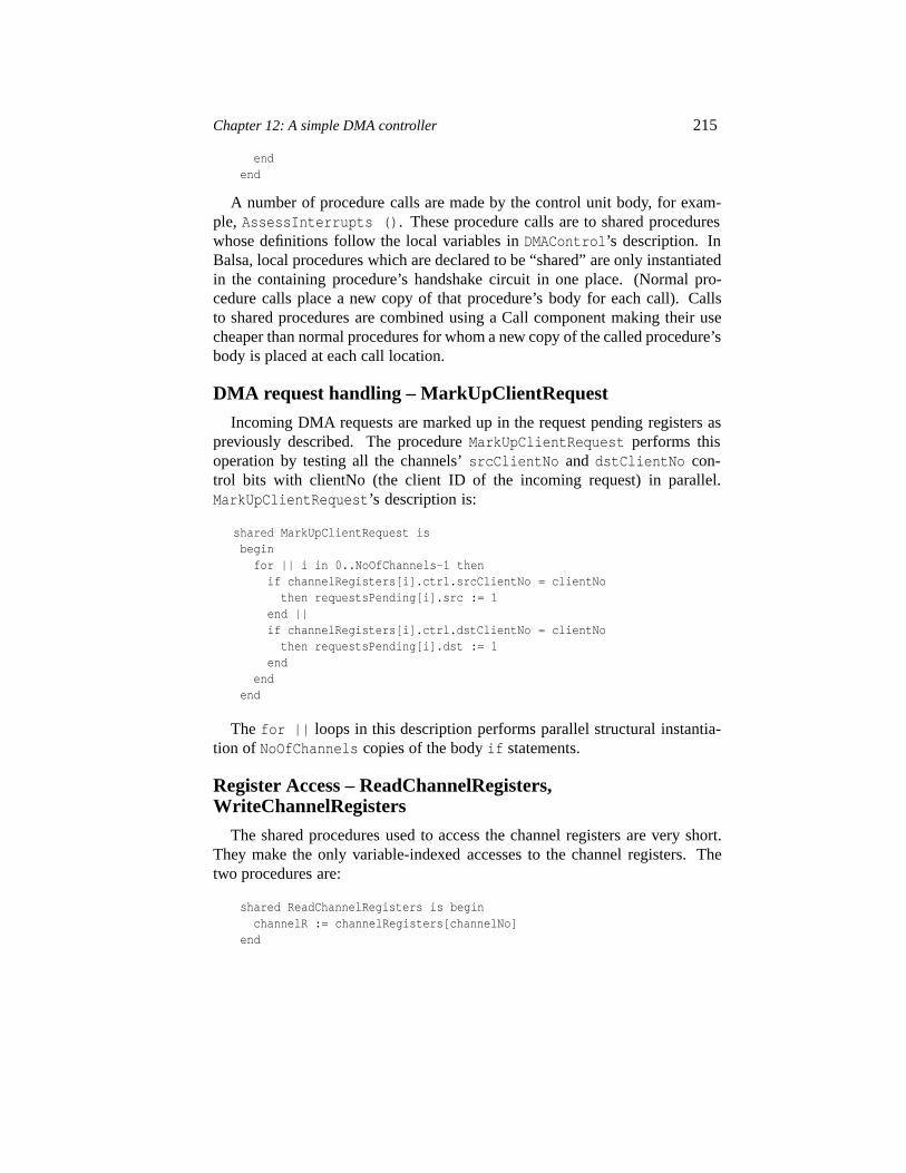
Chapter 12: A simple DMA controller 215
endend
A number of procedure calls are made by the control unit body, for exam-ple, AssessInterrupts (). These procedure calls are to shared procedureswhose definitions follow the local variables inDMAControl’s description. InBalsa, local procedures which are declared to be “shared” are only instantiatedin the containing procedure’s handshake circuit in one place. (Normal pro-cedure calls place a new copy of that procedure’s body for each call). Callsto shared procedures are combined using a Call component making their usecheaper than normal procedures for whom a new copy of the called procedure’sbody is placed at each call location.
DMA request handling – MarkUpClientRequest
Incoming DMA requests are marked up in the request pending registers aspreviously described. The procedureMarkUpClientRequest performs thisoperation by testing all the channels’srcClientNo anddstClientNo con-trol bits with clientNo (the client ID of the incoming request) in parallel.MarkUpClientRequest’s description is:
shared MarkUpClientRequest isbeginfor || i in 0..NoOfChannels-1 then
if channelRegisters[i].ctrl.srcClientNo = clientNothen requestsPending[i].src := 1
end ||if channelRegisters[i].ctrl.dstClientNo = clientNothen requestsPending[i].dst := 1
endend
end
Thefor || loops in this description performs parallel structural instantia-tion of NoOfChannels copies of the bodyif statements.
Register Access – ReadChannelRegisters,WriteChannelRegisters
The shared procedures used to access the channel registers are very short.They make the only variable-indexed accesses to the channel registers. Thetwo procedures are:
shared ReadChannelRegisters is beginchannelR := channelRegisters[channelNo]
end
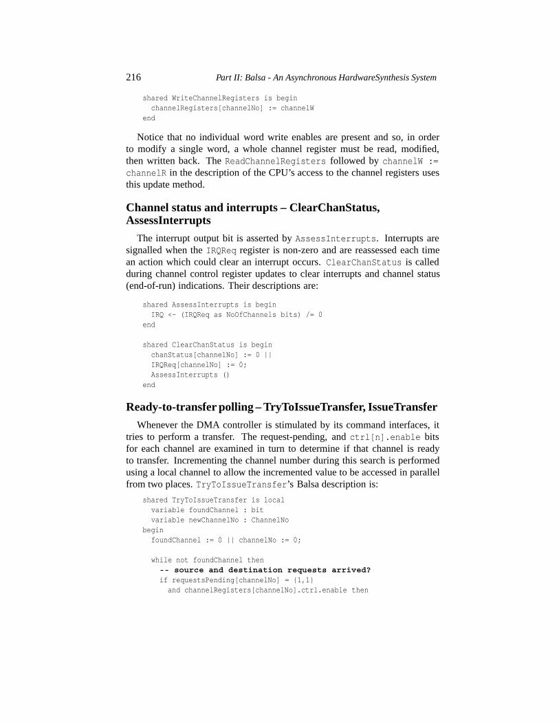
216 Part II: Balsa - An Asynchronous HardwareSynthesis System
shared WriteChannelRegisters is beginchannelRegisters[channelNo] := channelW
end
Notice that no individual word write enables are present and so, in orderto modify a single word, a whole channel register must be read, modified,then written back. TheReadChannelRegisters followed by channelW :=channelR in the description of the CPU’s access to the channel registers usesthis update method.
Channel status and interrupts – ClearChanStatus,AssessInterrupts
The interrupt output bit is asserted byAssessInterrupts. Interrupts aresignalled when theIRQReq register is non-zero and are reassessed each timean action which could clear an interrupt occurs.ClearChanStatus is calledduring channel control register updates to clear interrupts and channel status(end-of-run) indications. Their descriptions are:
shared AssessInterrupts is beginIRQ <- (IRQReq as NoOfChannels bits) /= 0
end
shared ClearChanStatus is beginchanStatus[channelNo] := 0 ||IRQReq[channelNo] := 0;AssessInterrupts ()
end
Ready-to-transfer polling – TryToIssueTransfer, IssueTransfer
Whenever the DMA controller is stimulated by its command interfaces, ittries to perform a transfer. The request-pending, andctrl[n].enable bitsfor each channel are examined in turn to determine if that channel is readyto transfer. Incrementing the channel number during this search is performedusing a local channel to allow the incremented value to be accessed in parallelfrom two places.TryToIssueTransfer’s Balsa description is:
shared TryToIssueTransfer is localvariable foundChannel : bitvariable newChannelNo : ChannelNo
beginfoundChannel := 0 || channelNo := 0;
while not foundChannel then-- source and destination requests arrived?if requestsPending[channelNo] = {1,1}and channelRegisters[channelNo].ctrl.enable then
Chapter 12: A simple DMA controller 217
ReadChannelRegisters ();requestsPending[channelNo] :=channelR.ctrl.srcDRQ, channelR.ctrl.dstDRQ ||
foundChannel := 1 ||IssueTransfer () ||UpdateRegistersAfterTransfer ()
elselocalchannel incChanNo : array ChannelNoLen + 1 of bit
beginincChanNo <- (channelNo + 1 asarray ChannelNoLen + 1 of bit) ||
select incChanNo thenfoundChannel := incChanNo[ChannelNoLen] ||newChannelNo := (incChanNo[0..ChannelNoLen-1]as ChannelNo)
end;channelNo := newChannelNo
endend
endend
Notice that if a transfer is taken, therequestPending bits for that chan-nel are re-initialised from thectrl.�srcDRQ,dstDRQ� control bits for thatchannel. The procedureIssueTransfer actually passes the transfer on to thetransfer engine. Its definition is:
shared IssueTransfer is beginTEBusy := 1 ||TECommand <- {channelR.src, channelR.dst}
end
The interlock formed by checkingTEBusy before attempting a transfer, andthe setting/resetting ofTEBusy by transfer initiation/completion ensures thatno transfer is presented to the transfer engine (deadlocking the control unit)while it is occupied. TheTEAck communication back to the control unit alsoprovides stimuli for re-triggering the DMA controller to perform outstandingrequests. This re-triggering, combined with the sequential polling of channels,allows outstanding requests (received while the transfer engine was busy) to beserviced correctly. Notice that a static prioritisation on pre-arrived requests isenforced by sequential channel polling.
Register increment/decrement –UpdateRegistersAfterTransfer
After a transfer has been issued, the registers for that transfer’s channel mustbe updated. ProcedureUpdateRegistersAfterTransfer performs this task:
218 Part II: Balsa - An Asynchronous HardwareSynthesis System
shared UpdateRegistersAfterTransfer is beginchannelW.ctrl := channelR.ctrl ||if channelR.ctrl.srcInc thenchannelW.src := (channelR.src + 1 as Word)
end ||if channelR.ctrl.dstInc thenchannelW.dst := (channelR.dst + 1 as Word)
end ||if channelR.ctrl.countDec thenchannelW.count := (channelR.count - 1 as Word)
end;if channelW.count = 0 thenchanStatus[channelNo] := 1 ||if IRQMask[channelNo] thenIRQReq[channelNo] := 1
end ||channelW.ctrl.enable := 0
end;WriteChannelRegisters ()
end
This procedure uses two incrementers and a decrementer to modify thechannel’s source address, destination address and count respectively. If thechannel’s transfer count is decremented to zero, thechanStatus bit, interruptstatus and channel enable are all updated to indicate an end-of-run.
This concludes the descriptions of the more illustrative aspects of the BalsaDMA controller description. For further details see [8] and, as was noted atthe beginning of this chapter, a full code listing is available from [7].
III
LARGE-SCALE ASYNCHRONOUS DESIGNS
Abstract In this final part of the book we describe some large-scale asynchronous VLSIdesigns to illustrate the capabilities of this technology. The first two of thesedesigns – the contactless smart card chip developed at Philips and the Viterbidecoder developed at the University of Manchester – were designed within EU-funded projects in the low-power design initiative that is the sponsor of this bookseries. The third chapter describes aspects of the Amulet microprocessor series,again from the University of Manchester, developed in several other EU-fundedprojects which, although outside the low-power design initiative, never-the-lessstill had low power as a significant objective.The chips descibed in this part of the book are some of the largest and most com-plex asynchronous designs ever developed. Fully detailed descriptions of themare far beyond the scope of this book, but they are included to demonstrate thatasynchronous design is fully capable of supporting large-scale designs, and theyshow what can be done with skilled and experienced design teams. The descrip-tions presented here have been written to give insight into the thinking processesthat a designer of state-of-the-art asynchronous systems might go through in de-veloping such designs.
Keywords: asynchronous circuits, large-scale designs

Chapter 13
DESCALE: �
a Design Experiment for a Smart Card Applicationconsuming Low Energy
Joep Kessels & Ad PeetersPhilips Research, NL-5656AA Eindhoven, The Netherlands
{Joep.Kessels � Ad.Peeters}@philips.com
Torsten KramerKramer-Consulting, D-21079 Hamburg, Germany
Volker TimmPhilips Semiconductors, D-22529 Hamburg, Germany
Abstract We have designed an asynchronous chip for contactless smart cards. Asyn-chronous circuits have two power properties that make them very suitable forcontactless devices: low average power and small current peaks. The fact thatasynchronous circuits operate over a wide range of the supply voltage, whileautomatically adapting their speed, has been used to obtain a circuit that is veryresilient to voltage drops while giving maximum performance for the power be-ing received. The asynchronous circuit has been built, tested and evaluated.
Keywords: low-power asynchronous circuits, smart cards, contactless devices, DES cryp-tography
�Part of the work described in this paper was funded by the European Commission under Esprit TCS/ESD-LPD contract 25519 (Design Experiment DESCALE).
221
222 Part III: Large-Scale Asynchronous Designs
13.1. Introduction
Since their introduction in the eighties, smart cards have been used in a con-tinuously growing number of applications, such as banking, telephony (tele-phone and SIM cards), access control (Pay-TV), health-care, tickets for publictransport, electronic signatures, and identification. Currently, most cards havecontacts and, for that reason, need to be inserted into a reader. For applicationsin which the fast handling of transactions is important,contactless smart cardshave been introduced requiring only close proximity to a reader (typically sev-eral centimeters). The chip on such a card must be extremely power efficient,since it is powered by electromagnetic radiation.
Asynchronous CMOS circuits have the potential for very low power con-sumption, since they only dissipate when and where active. However, asyn-chronous circuits are difficult to design at the level of gates and registers.Therefore the high-level design language Tangram was defined [141] and asilicon compiler has been implemented that translates Tangram programs intoasynchronous circuits.
The Tangram compiler generates a special class of asynchronous circuitscalled handshake circuits [135, 112]. Handshake circuits are constructed froma set of about forty basic components that use handshake signalling for com-munication.
Several chips have been designed in Tangram [136, 144] and if we comparethese chips to existing clocked implementations, then the asynchronous ver-sions are generally about 20% larger in area and consume about 25% of thepower.
In order to find out what advantages asynchronous circuits have to offer incontactless smart cards, we have designed an asynchronous smart card chip. Inthis chapter, we indicate which properties of asynchronous circuits have beenexploited and we present the results. The rest of the chapter is organized as fol-lows. Section 13.2 presents the Tangram method for designing asynchronouscircuits. Section 13.3 summarizes the differences in power behaviour betweensynchronous and asynchronous circuits. Section 13.4 first provides some back-ground to contactless smart cards, then identifies the power characteristics inwhich contactless devices differ from battery-powered ones, and finally indi-cates why asynchronous circuits are very suited for contactless devices. Sec-tion 13.5 presents the digital circuit, Section 13.6 the results of the silicon, andSection 13.8 the power regulator, which also exploits an asynchronous oppor-tunity. We conclude with a summary of the merits of this asynchronous design.
Chapter 13: Descale 223
13.2. VLSI programming of asynchronous circuits
The design flow that is used in the design of the smart card IC reported hereis based on the programming language Tangram and its associated compilerand tool set. An important aspect of this design approach is thetransparencyof the silicon compiler [142], which allows the designer to reason about de-sign characteristics such as area, power, performance, and testability, at theprogramming (Tangram) level.
This section first introduces the Tangram tool set, then briefly describes theunderlying handshake technology, and finally illustrates VLSI-programmingtechniques using the GCD algorithm presented in Chapter 8.
13.2.1 The Tangram toolset
Fig. 13.1 shows the Tangram toolset. The designer describes a design inTangram, which is a conventional programming language, similar to C andPascal, extended to include constructs for expressing concurrency and com-munication in a way similar to those in the language CSP [58]. In addition tothis, there are language constructs for expressing hardware-specific issues, likesharing of blocks and waiting for clock-edges.
A compiler translates Tangram programs into so-calledhandshake circuits,which are netlists composed from a library of some 40 handshake components.Each handshake component implements a language construct, such as sequenc-ing, repetition, communication, and sharing.
The handshake circuit simulator and corresponding performance analyzergive feedback to the designer about aspects such as function, area, timing,power, and testability.
The actual mapping onto a conventional (synchronous) standard-cell libraryis done in two steps. In the first step the component expander uses the com-ponent library to generate an abstract netlist consisting of combinational logic,registers, and asynchronous cells, such as Muller C-elements. This step alsodetermines the data encoding and the handshake protocol; generally a four-phase single-rail implementation is generated. In the second step commercialsynthesis tools and technology mappers are used to generate the standard-cellnetlist. No dedicated (asynchronous) cells are required in this mapping, be-cause all asynchronous cells are decomposed into cells from the standard-celllibrary at hand.
Similar language-based approaches using handshake circuits as intermedi-ate format are described in [17, 9]. Design approaches in which asynchronousdetails are not hidden from the designer have also proven successful [80, 21,83, 30, 64]. A general overview of design methods for asynchronous circuitsis given in [69] and in Part I of this book.
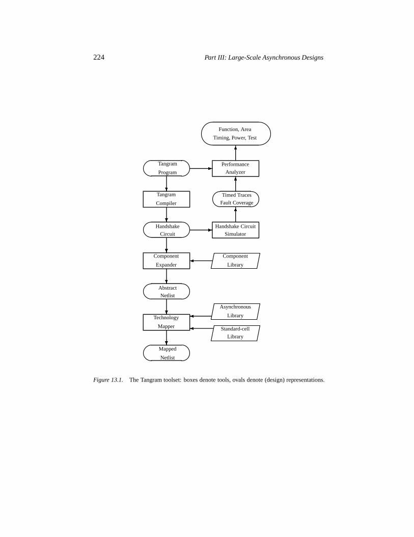
224 Part III: Large-Scale Asynchronous Designs
Tangram
Program
Tangram
Compiler
Handshake
Circuit
Component
Expander
Abstract
Netlist
Technology
Mapper
Mapped
Netlist
�
�
�
�
�
�
Function, Area
Timing, Power, Test
Performance
Analyzer
Timed Traces
Fault Coverage
Handshake Circuit
Simulator
�
�
�
�
�
�
�
�
Component
Library
Asynchronous
Library
Standard-cell
Library
Figure 13.1. The Tangram toolset: boxes denote tools, ovals denote (design) representations.
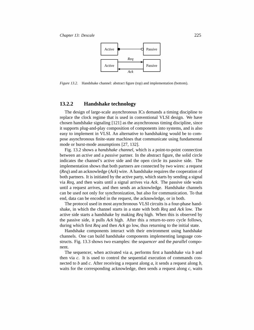
Chapter 13: Descale 225
Active Passive
Active Passive�Req
�Ack
Figure 13.2. Handshake channel: abstract figure (top) and implementation (bottom).
13.2.2 Handshake technology
The design of large-scale asynchronous ICs demands a timing discipline toreplace the clock regime that is used in conventional VLSI design. We havechosen handshake signaling [121] as the asynchronous timing discipline, sinceit supports plug-and-play composition of components into systems, and is alsoeasy to implement in VLSI. An alternative to handshaking would be to com-pose asynchronous finite-state machines that communicate using fundamentalmode or burst-mode assumptions [27, 132].
Fig. 13.2 shows ahandshake channel, which is a point-to-point connectionbetween anactive and apassive partner. In the abstract figure, the solid circleindicates the channel’s active side and the open circle its passive side. Theimplementation shows that both partners are connected by two wires: a request(Req) and an acknowledge (Ack) wire. A handshake requires the cooperation ofboth partners. It is initiated by the active party, which starts by sending a signalvia Req, and then waits until a signal arrives viaAck. The passive side waitsuntil a request arrives, and then sends an acknowledge. Handshake channelscan be used not only for synchronization, but also for communication. To thatend, data can be encoded in the request, the acknowledge, or in both.
The protocol used in most asynchronous VLSI circuits is a four-phase hand-shake, in which the channel starts in a state with bothReq andAck low. Theactive side starts a handshake by makingReq high. When this is observed bythe passive side, it pullsAck high. After this a return-to-zero cycle follows,during which firstReq and thenAck go low, thus returning to the initial state.
Handshake components interact with their environment using handshakechannels. One can build handshake components implementing language con-structs. Fig. 13.3 shows two examples: thesequencer and theparallel compo-nent.
The sequencer, when activated viaa, performs first a handshake viab andthen viac. It is used to control the sequential execution of commands con-nected tob andc. After receiving a request alonga, it sends a request alongb,waits for the corresponding acknowledge, then sends a request alongc, waits
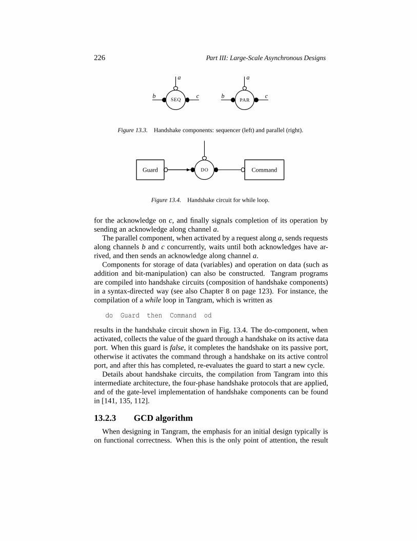
226 Part III: Large-Scale Asynchronous Designs
SEQ
a
cbPAR
a
cb
Figure 13.3. Handshake components: sequencer (left) and parallel (right).
Guard CommandDO�
Figure 13.4. Handshake circuit for while loop.
for the acknowledge onc, and finally signals completion of its operation bysending an acknowledge along channela.
The parallel component, when activated by a request alonga, sends requestsalong channelsb andc concurrently, waits until both acknowledges have ar-rived, and then sends an acknowledge along channela.
Components for storage of data (variables) and operation on data (such asaddition and bit-manipulation) can also be constructed. Tangram programsare compiled into handshake circuits (composition of handshake components)in a syntax-directed way (see also Chapter 8 on page 123). For instance, thecompilation of awhile loop in Tangram, which is written as
do Guard then Command od
results in the handshake circuit shown in Fig. 13.4. The do-component, whenactivated, collects the value of the guard through a handshake on its active dataport. When this guard isfalse, it completes the handshake on its passive port,otherwise it activates the command through a handshake on its active controlport, and after this has completed, re-evaluates the guard to start a new cycle.
Details about handshake circuits, the compilation from Tangram into thisintermediate architecture, the four-phase handshake protocols that are applied,and of the gate-level implementation of handshake components can be foundin [141, 135, 112].
13.2.3 GCD algorithm
When designing in Tangram, the emphasis for an initial design typically ison functional correctness. When this is the only point of attention, the result
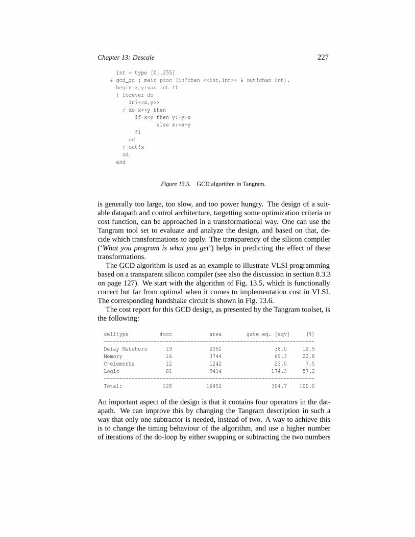
Chapter 13: Descale 227
int = type [0..255]& gcd_gc : main proc (in?chan <<int,int>> & out!chan int).begin x,y:var int ff| forever do
in?<<x,y>>; do x<>y then
if x<y then y:=y-xelse x:=x-y
fiod
; out!xod
end
Figure 13.5. GCD algorithm in Tangram.
is generally too large, too slow, and too power hungry. The design of a suit-able datapath and control architecture, targetting some optimization criteria orcost function, can be approached in a transformational way. One can use theTangram tool set to evaluate and analyze the design, and based on that, de-cide which transformations to apply. The transparency of the silicon compiler(‘What you program is what you get’) helps in predicting the effect of thesetransformations.
The GCD algorithm is used as an example to illustrate VLSI programmingbased on a transparent silicon compiler (see also the discussion in section 8.3.3on page 127). We start with the algorithm of Fig. 13.5, which is functionallycorrect but far from optimal when it comes to implementation cost in VLSI.The corresponding handshake circuit is shown in Fig. 13.6.
The cost report for this GCD design, as presented by the Tangram toolset, isthe following:
celltype #occ area gate eq. [eqv] (%)--------------------------------------------------------------------Delay Matchers 19 2052 38.0 12.5Memory 16 3744 69.3 22.8C-elements 12 1242 23.0 7.5Logic 81 9414 174.3 57.2--------------------------------------------------------------------Total: 128 16452 304.7 100.0
An important aspect of the design is that it contains four operators in the dat-apath. We can improve this by changing the Tangram description in such away that only one subtractor is needed, instead of two. A way to achieve thisis to change the timing behaviour of the algorithm, and use a higher numberof iterations of the do-loop by either swapping or subtracting the two numbers
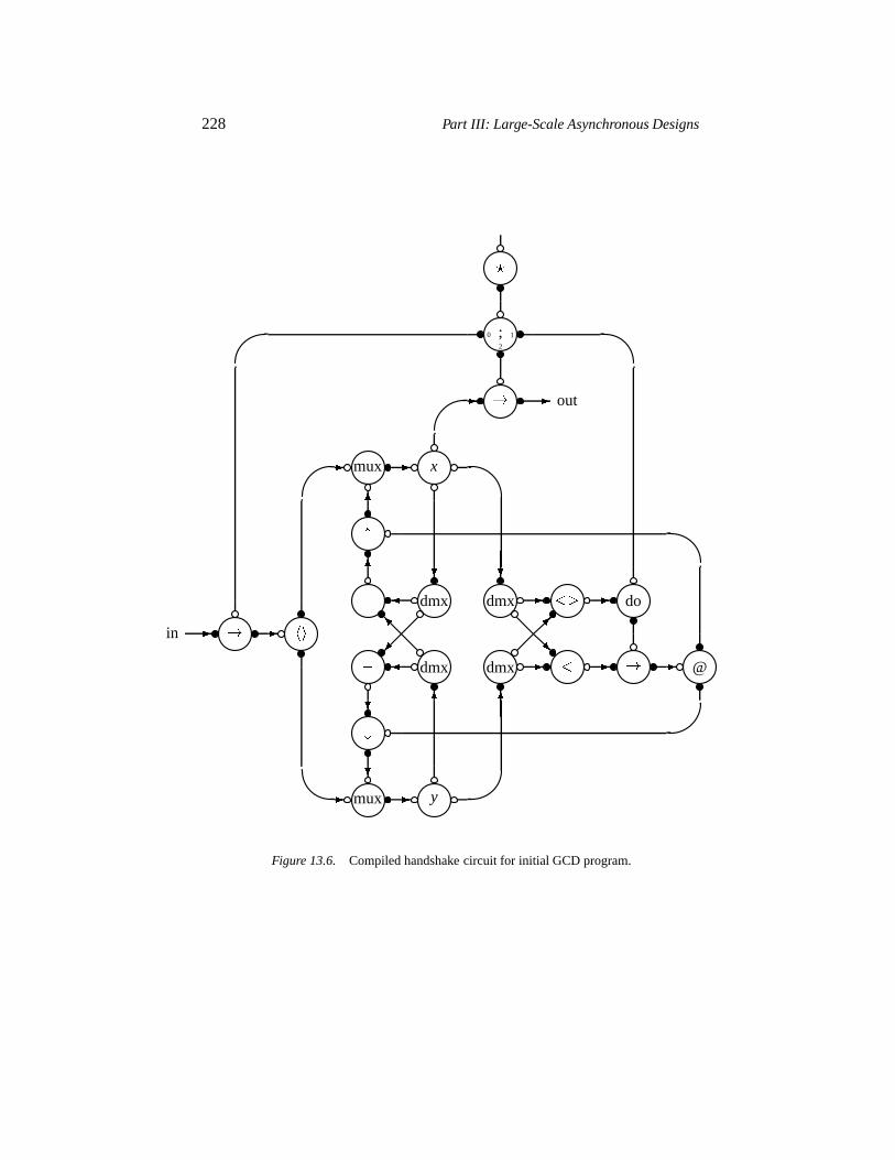
228 Part III: Large-Scale Asynchronous Designs
mux
�
� y�
�
� ��
dmx
�
dmx
�
�
��
mux
�
� x�
�
� �
�
dmx
�
dmx
�
��
�
� do�
�� @�
��in ���
� � out�
;0 1
2
�
Figure 13.6. Compiled handshake circuit for initial GCD program.
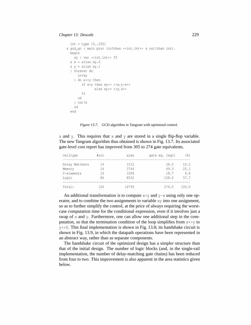
Chapter 13: Descale 229
int = type [0..255]& gcd_gc : main proc (in?chan <<int,int>> & out!chan int).begin
xy : var <<int,int>> ff& x = alias xy.0& y = alias xy.1| forever do
in?xy; do x<>y then
if x<y then xy:= <<x,y-x>>else xy:= <<y,x>>
fiod
; out!xod
end
Figure 13.7. GCD algorithm in Tangram with optimized control.
x andy. This requires thatx andy are stored in a single flip-flop variable.The new Tangram algorithm thus obtained is shown in Fig. 13.7. Its associatedgate-level cost report has improved from 305 to 274 gate equivalents.
celltype #occ area gate eq. [eqv] (%)--------------------------------------------------------------------Delay Matchers 14 1512 28.0 10.2Memory 16 3744 69.3 25.3C-elements 10 1008 18.7 6.8Logic 86 8532 158.0 57.7--------------------------------------------------------------------Total: 126 14796 274.0 100.0
An additional transformation is to computex<y andy-x using only one op-erator, and to combine the two assignments to variablexy into one assignment,so as to further simplify the control, at the price of always requiring the worst-case computation time for the conditional expression, even if it involves just aswap ofx andy. Furthermore, one can allow one additional step in the com-putation, so that the termination condition of the loop simplifies fromx<>y toy<>0. This final implementation is shown in Fig. 13.8; its handshake circuit isshown in Fig. 13.9, in which the datapath operations have been represented inan abstract way, rather than as separate components.
The handshake circuit of the optimized design has a simpler structure thanthat of the initial design. The number of logic blocks (and, in the single-railimplementation, the number of delay-matching gate chains) has been reducedfrom four to two. This improvement is also apparent in the area statistics givenbelow.
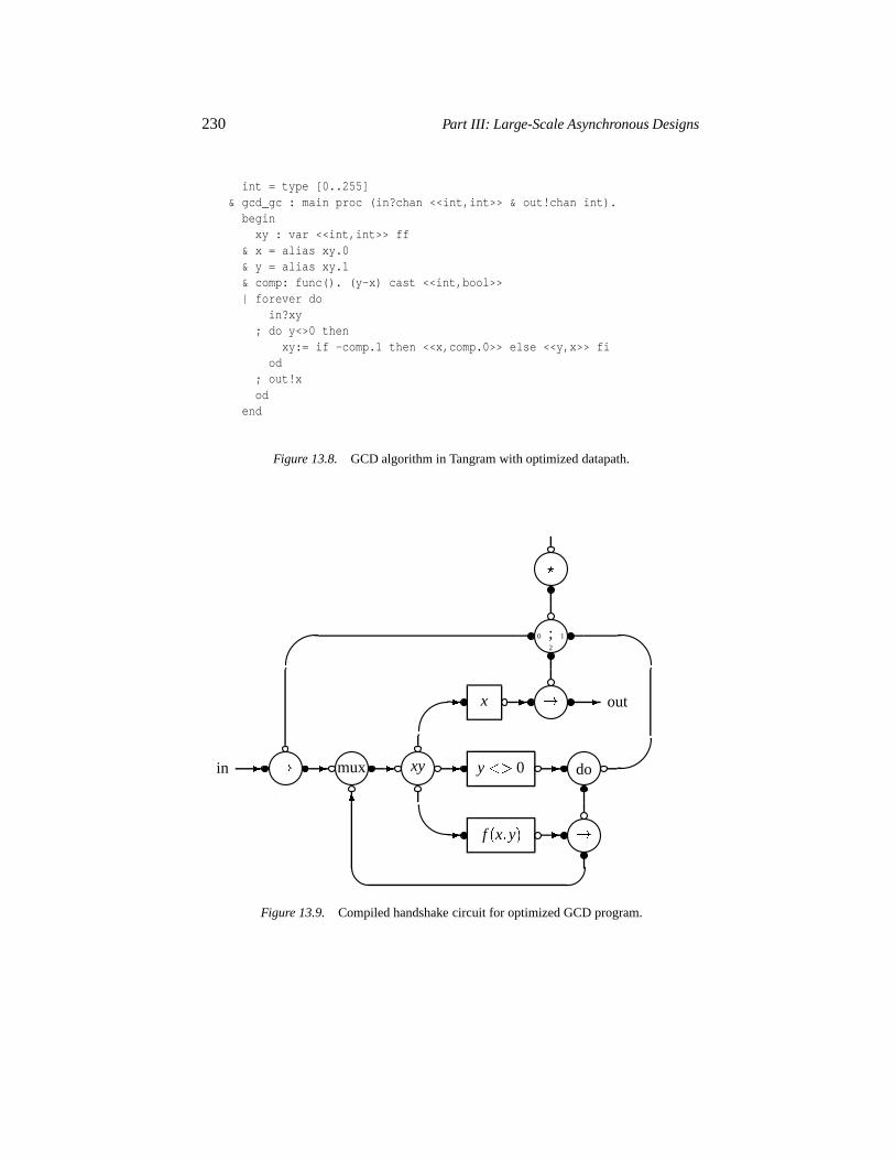
230 Part III: Large-Scale Asynchronous Designs
int = type [0..255]& gcd_gc : main proc (in?chan <<int,int>> & out!chan int).
beginxy : var <<int,int>> ff
& x = alias xy.0& y = alias xy.1& comp: func(). (y-x) cast <<int,bool>>| forever do
in?xy; do y<>0 then
xy:= if -comp.1 then <<x,comp.0>> else <<y,x>> fiod
; out!xod
end
Figure 13.8. GCD algorithm in Tangram with optimized datapath.
��in mux
�
� xy�
x�
y �� 0�
f �x�y��
�� � out
do�
��
;0 1
2
�
Figure 13.9. Compiled handshake circuit for optimized GCD program.
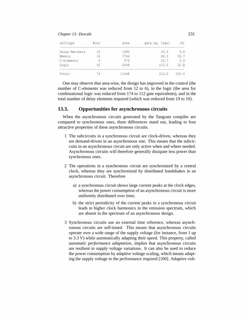
Chapter 13: Descale 231
celltype #occ area gate eq. [eqv] (%)--------------------------------------------------------------------Delay Matchers 10 1080 20.0 9.4Memory 16 3744 69.3 32.7C-elements 6 576 10.7 5.0Logic 42 6048 112.0 52.8--------------------------------------------------------------------Total: 74 11448 212.0 100.0
One may observe that area-wise, the design has improved in the control (thenumber of C-elements was reduced from 12 to 6), in the logic (the area forcombinational logic was reduced from 174 to 112 gate equivalents), and in thetotal number of delay elements required (which was reduced from 19 to 10).
13.3. Opportunities for asynchronous circuits
When the asynchronous circuits generated by the Tangram compiler arecompared to synchronous ones, three differences stand out, leading to fourattractive properties of these asynchronous circuits.
1 The subcircuits in a synchronous circuit are clock-driven, whereas theyare demand-driven in an asynchronous one. This means that the subcir-cuits in an asynchronous circuit are only active when and where needed.Asynchronous circuits will therefore generally dissipate less power thansynchronous ones.
2 The operations in a synchronous circuit are synchronized by a centralclock, whereas they are synchronized by distributed handshakes in anasynchronous circuit. Therefore
a) a synchronous circuit shows large current peaks at the clock edges,whereas the power consumption of an asynchronous circuit is moreuniformly distributed over time;
b) the strict periodicity of the current peaks in a synchronous circuitleads to higher clock harmonics in the emission spectrum, whichare absent in the spectrum of an asynchronous design.
3 Synchronous circuits use an external time reference, whereas asynch-ronous circuits are self-timed. This means that asynchronous circuitsoperate over a wide range of the supply voltage (for instance, from 1 upto 3.3 V) while automatically adapting their speed. This property, calledautomatic performance adaptation, implies that asynchronous circuitsare resilient to supply voltage variations. It can also be used to reducethe power consumption by adaptive voltage scaling, which means adapt-ing the supply voltage to the performance required [100]. Adaptive volt-
232 Part III: Large-Scale Asynchronous Designs
age scaling techniques are also applied in synchronous circuits, but thenspecial measures must be taken to adapt the clock frequency.
Asynchronous circuits also have drawbacks. The most important one is thatthese circuits are unconventional: designers and mainstream tools and librariesare all oriented towards synchronous design methods. Additional drawbacksof asynchronous circuits come from the fact that they use gates to control reg-isters (latches and flip-flops), instead of the relatively straightforward clock-distribution network in synchronous circuits. Although this enables the lowpower consumption it also leads to circuits that are typically larger, slower,and harder to test. Testability (for fabrication defects) is probably the mostfundamental issue of these. For a discussion on testing asynchronous circuitswe refer to [61, 120].
Property 2.b was the main reason for Philips Semiconductors to design afamily of asynchronous pager chips [114]. However, as is addressed in the nextsection, it is the other three properties that can be used most advantageously incontactless smart card chips.
13.4. Contactless smartcards
Contactless smart cards have a number of advantages when compared tocontacted ones: they are convenient and fast to use, insensitive to dirt andgrease and, since their readers have no slots, they are less amenable to vandal-ism.
The communication between a contactless smart card and reader is estab-lished through an electromagnetic field, emitted by the reader. The card has acoil through which it can retrieve energy from this field. The amount of energythat can be retrieved depends on the distance to the reader, the number of turnsin the coil, and the orientation of the card in the field.
Fig. 13.10 shows the functional parts of a contactless smartcard consistingof a VLSI circuit (in the dotted box) and an external coil. The tuned circuitformed by the coil and capacitorC0 is used for three purposes:
receiving power;
receiving the clock frequency (equal to the carrier frequency); and
supporting the communication.
The complete circuit consists of a power supply unit and a digital circuit witha buffer capacitor (C1) for storing energy.
Several standards for contactless smart cards currently exist:
ISO/IEC 10536, which specifiesclose coupling cards, operating at a dis-tance of 1cm from the reader.
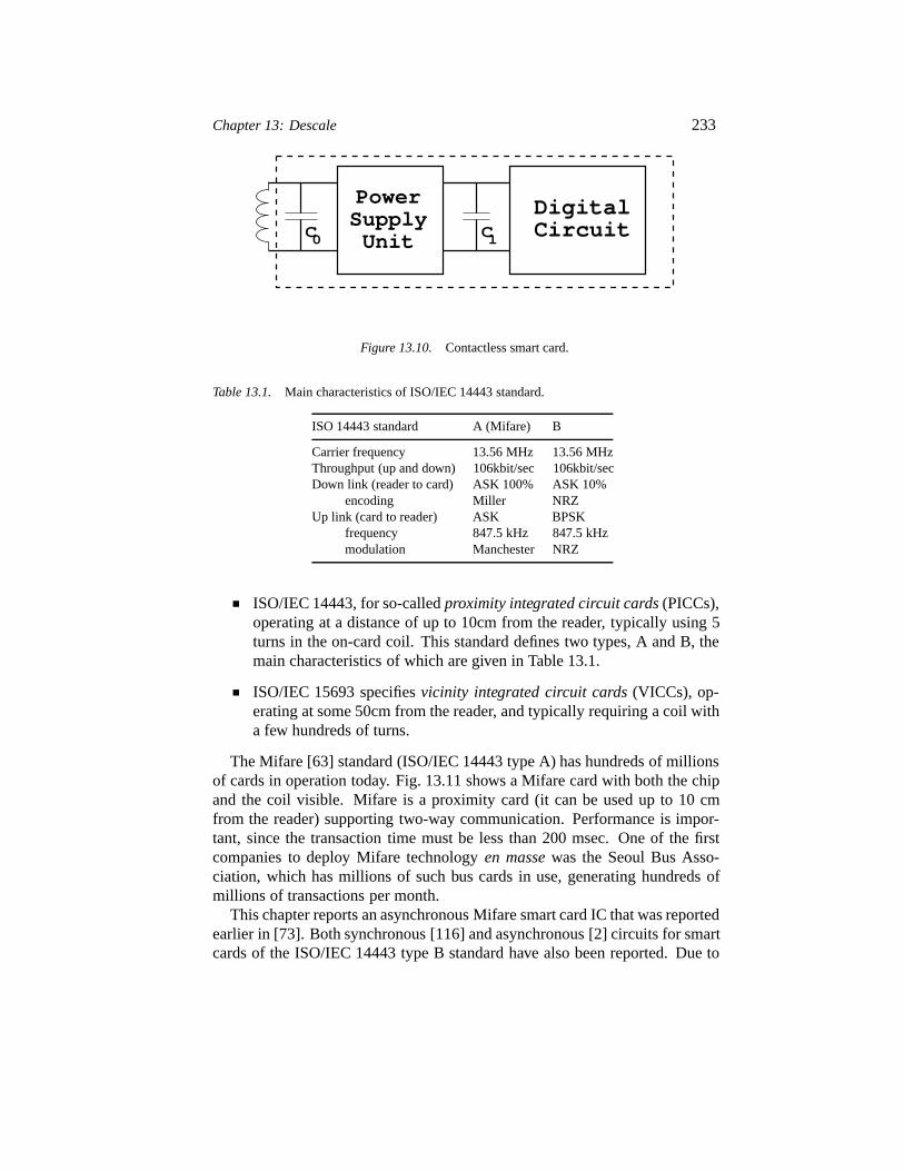
Chapter 13: Descale 233
DigitalCircuit
PowerSupplyUnitC0 C1
Figure 13.10. Contactless smart card.
Table 13.1. Main characteristics of ISO/IEC 14443 standard.
ISO 14443 standard A (Mifare) B
Carrier frequency 13.56 MHz 13.56 MHzThroughput (up and down) 106kbit/sec 106kbit/secDown link (reader to card) ASK 100% ASK 10%
encoding Miller NRZUp link (card to reader) ASK BPSK
frequency 847.5 kHz 847.5 kHzmodulation Manchester NRZ
ISO/IEC 14443, for so-calledproximity integrated circuit cards (PICCs),operating at a distance of up to 10cm from the reader, typically using 5turns in the on-card coil. This standard defines two types, A and B, themain characteristics of which are given in Table 13.1.
ISO/IEC 15693 specifiesvicinity integrated circuit cards (VICCs), op-erating at some 50cm from the reader, and typically requiring a coil witha few hundreds of turns.
The Mifare [63] standard (ISO/IEC 14443 type A) has hundreds of millionsof cards in operation today. Fig. 13.11 shows a Mifare card with both the chipand the coil visible. Mifare is a proximity card (it can be used up to 10 cmfrom the reader) supporting two-way communication. Performance is impor-tant, since the transaction time must be less than 200 msec. One of the firstcompanies to deploy Mifare technologyen masse was the Seoul Bus Asso-ciation, which has millions of such bus cards in use, generating hundreds ofmillions of transactions per month.
This chapter reports an asynchronous Mifare smart card IC that was reportedearlier in [73]. Both synchronous [116] and asynchronous [2] circuits for smartcards of the ISO/IEC 14443 type B standard have also been reported. Due to
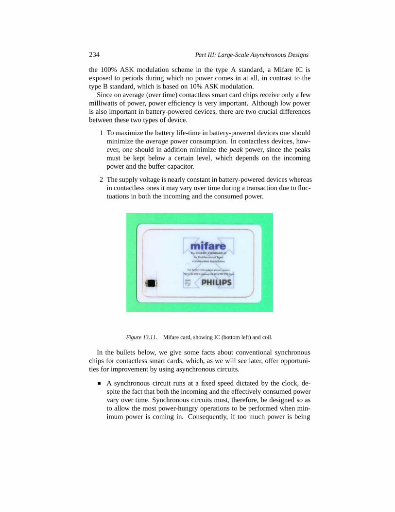
234 Part III: Large-Scale Asynchronous Designs
the 100% ASK modulation scheme in the type A standard, a Mifare IC isexposed to periods during which no power comes in at all, in contrast to thetype B standard, which is based on 10% ASK modulation.
Since on average (over time) contactless smart card chips receive only a fewmilliwatts of power, power efficiency is very important. Although low poweris also important in battery-powered devices, there are two crucial differencesbetween these two types of device.
1 To maximize the battery life-time in battery-powered devices one shouldminimize theaverage power consumption. In contactless devices, how-ever, one should in addition minimize thepeak power, since the peaksmust be kept below a certain level, which depends on the incomingpower and the buffer capacitor.
2 The supply voltage is nearly constant in battery-powered devices whereasin contactless ones it may vary over time during a transaction due to fluc-tuations in both the incoming and the consumed power.
Figure 13.11. Mifare card, showing IC (bottom left) and coil.
In the bullets below, we give some facts about conventional synchronouschips for contactless smart cards, which, as we will see later, offer opportuni-ties for improvement by using asynchronous circuits.
A synchronous circuit runs at a fixed speed dictated by the clock, de-spite the fact that both the incoming and the effectively consumed powervary over time. Synchronous circuits must, therefore, be designed so asto allow the most power-hungry operations to be performed when min-imum power is coming in. Consequently, if too much power is being
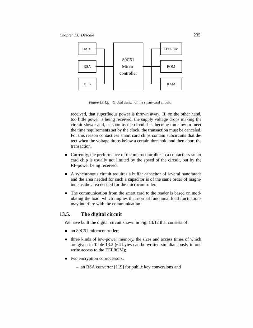
Chapter 13: Descale 235
DES
RSA
UART
80C51
Micro-
controller
RAM
ROM
EEPROM
Figure 13.12. Global design of the smart-card circuit.
received, that superfluous power is thrown away. If, on the other hand,too little power is being received, the supply voltage drops making thecircuit slower and, as soon as the circuit has become too slow to meetthe time requirements set by the clock, the transaction must be canceled.For this reason contactless smart card chips contain subcircuits that de-tect when the voltage drops below a certain threshold and then abort thetransaction.
Currently, the performance of the microcontroller in a contactless smartcard chip is usually not limited by the speed of the circuit, but by theRF-power being received.
A synchronous circuit requires a buffer capacitor of several nanofaradsand the area needed for such a capacitor is of the same order of magni-tude as the area needed for the microcontroller.
The communication from the smart card to the reader is based on mod-ulating the load, which implies that normal functional load fluctuationsmay interfere with the communication.
13.5. The digital circuit
We have built the digital circuit shown in Fig. 13.12 that consists of:
an 80C51 microcontroller;
three kinds of low-power memory, the sizes and access times of whichare given in Table 13.2 (64 bytes can be written simultaneously in onewrite access to the EEPROM);
two encryption coprocessors:
– an RSA converter [119] for public key conversions and

236 Part III: Large-Scale Asynchronous Designs
– a triple DES converter [96] for private key conversions;
a UART for the external communication.
The EEPROM contains program parts as well as data such as encryption keysand e-money. Both the ROM and the RAM are equipped with matching delaylines and for the EEPROM we designed a similar function based on a counter.These delay lines have been used to provide all three memories with a hand-shake interface, which made it extremely easy to deal with the differences inaccess time as well as variations in both temperature and supply voltage. Anadditional advantage is that the controller automatically runs faster when exe-cuting code from ROM than when executing code from EEPROM.
The circuit is meant to be used in adual-interface card, which is a card withboth a contacted and a contactless interface. Apart from the RSA converter,which will not be used in contactless operation, all circuits are asynchronous.In contactless operation, the average supply voltage will be about 2 V. Thesimulations, however, are done at 3.3 V, which is the voltage at which thelibrary has been characterized.
Table 13.2. Memory sizes and access times.
Memory Size Access time [ns]type [kbyte] read write
RAM 2 10 10ROM 38 30EEPROM 32 180 4,000
13.5.1 The 80C51 microcontroller
The 80C51 microcontroller is a modified version of the one described in[144, 143]. The four most important modifications are described below.
To deal with the slow memories aprefetch unit has been included in the80C51 architecture. At 3.3 V the average instruction execution time in free-running mode is about 100 ns provided it takes no time to fetch the code frommemory. If, however, code is fetched from the EEPROM and the microcon-troller has to wait during the read accesses, the performance would be drasti-cally reduced, since most instructions are one or two bytes long, taking 180 or360 ns to fetch. To avoid this performance degradation a form ofinstructionprefetching has been introduced in which a process running concurrently tothe 80C51 core is fetching code bytes as long as a two byte FIFO is not full.
Chapter 13: Descale 237
The prefetch unit gives an increase in performance of about 30%. A simplifiedversion of the prefetch unit is described in Section 13.5.2.
We also introducedearly write completion, which means that the microcon-troller continues execution as soon as it has issued a write access. This hasbeen introduced to prevent the microcontroller from waiting during the 4 msecit takes to do a write access to the EEPROM (for instance to change the e-money), but also to speed up the write accesses to the RAM. To exploit thisfeature when doing a write access to the EEPROM, the corresponding codemust be in the ROM.
The controller has been provided with animmediate halt input signal bywhich its execution can be halted within a short time. This provision is nec-essary to deal with the fact that the information, which the reader sends to thecard, is coded by suppressing the carrier during periods of 3µsec. Since thecard does not receive any power during these periods, the controller has to behalted immediately (only some basic functions continue to operate). In thesynchronous design this halting function came naturally, since the clock wouldstop during these periods.
We have introduced aquasi synchronous mode, in which the microcontrolleris, at instruction level, fully timing compatible with its synchronous counter-part. In this mode, the asynchronous microcontroller waits after each instruc-tion until the number of clock ticks required by a synchronous version haveelapsed. This mode is necessary when time-dependent functions are designedin software. Since this mode is under software control, the microcontroller caneasily switch modes depending on the function it is executing. This featurewas also of great help to demonstrate theguaranteed performance, which isthe maximum clock rate at which each instruction terminates within the givennumber of clock ticks. For most programs, thefree-running performance isabout twice as high as the guaranteed performance.
We have compared the asynchronous circuit as compiled from Tangram witha synchronous circuit that is functionally equivalent, and which has been com-piled from synthesizable VHDL to the same CMOS technology. These ICshave a comparable performance. The asynchronous microcontroller nicelydemonstrates the three properties of asynchronous circuits that we want to ex-ploit in the design of the smart-card chip:
The average power consumption of the asynchronous 80C51 is aboutthree times lower than the power consumption of its synchronous coun-terpart when delivering the same performance at the same supply volt-age.
Fig. 13.13 shows the current peaks of both the synchronous and the asyn-chronous 80C51 at 3.3 V, where the asynchronous version is running inquasi synchronous mode, giving a performance that is 2.5 times higher
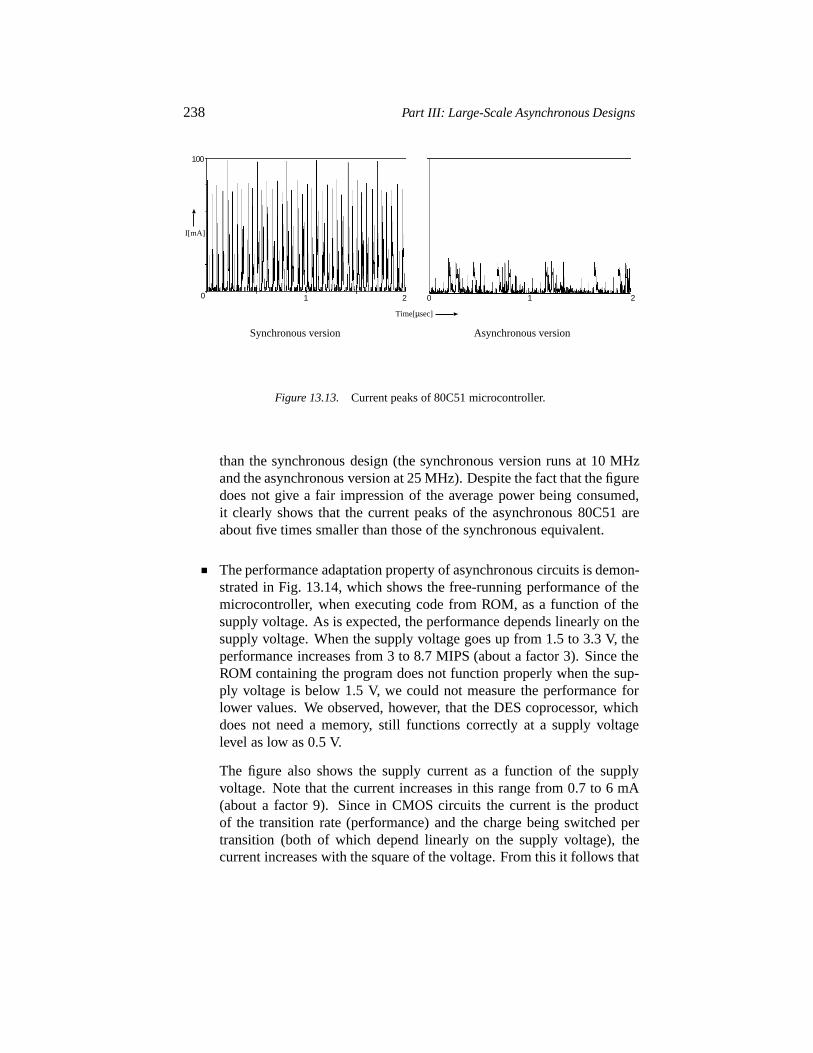
238 Part III: Large-Scale Asynchronous Designs
100
0 1 2 0 1 2
Time[µsec]
I[mA]
Synchronous version Asynchronous version
Figure 13.13. Current peaks of 80C51 microcontroller.
than the synchronous design (the synchronous version runs at 10 MHzand the asynchronous version at 25 MHz). Despite the fact that the figuredoes not give a fair impression of the average power being consumed,it clearly shows that the current peaks of the asynchronous 80C51 areabout five times smaller than those of the synchronous equivalent.
The performance adaptation property of asynchronous circuits is demon-strated in Fig. 13.14, which shows the free-running performance of themicrocontroller, when executing code from ROM, as a function of thesupply voltage. As is expected, the performance depends linearly on thesupply voltage. When the supply voltage goes up from 1.5 to 3.3 V, theperformance increases from 3 to 8.7 MIPS (about a factor 3). Since theROM containing the program does not function properly when the sup-ply voltage is below 1.5 V, we could not measure the performance forlower values. We observed, however, that the DES coprocessor, whichdoes not need a memory, still functions correctly at a supply voltagelevel as low as 0.5 V.
The figure also shows the supply current as a function of the supplyvoltage. Note that the current increases in this range from 0.7 to 6 mA(about a factor 9). Since in CMOS circuits the current is the productof the transition rate (performance) and the charge being switched pertransition (both of which depend linearly on the supply voltage), thecurrent increases with the square of the voltage. From this it follows that
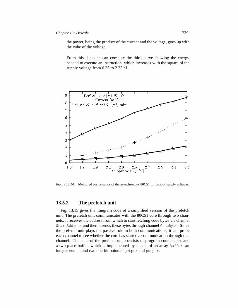
Chapter 13: Descale 239
the power, being the product of the current and the voltage, goes up withthe cube of the voltage.
From this data one can compute the third curve showing the energyneeded to execute an instruction, which increases with the square of thesupply voltage from 0.35 to 2.25 nJ.
�
�
�
�
�
�
�
�
��� ��� �� ��� ��� ��� ��� �� ��� ���� ���� ������� ���
����������� � !��� �
�
�
�
�
�
�
�
��
�" ����� ��#� �
��
��
��
�
�
�
�
$����� ��� %�&�� ��%�� ��'� �
� � � � � ��
��
�
Figure 13.14. Measured performance of the asynchronous 80C51 for various supply voltages.
13.5.2 The prefetch unit
Fig. 13.15 gives the Tangram code of a simplified version of the prefetchunit. The prefetch unit communicates with the 80C51 core through two chan-nels: it receives the address from which to start fetching code bytes via channelStartAddress and then it sends these bytes through channelCodeByte. Sincethe prefetch unit plays the passive role in both communications, it can probeeach channel to see whether the core has started a communication through thatchannel. The state of the prefetch unit consists of program counter,pc, anda two-place buffer, which is implemented by means of an arrayBuffer, anintegercount, and two one-bit pointersgetptr andputptr.
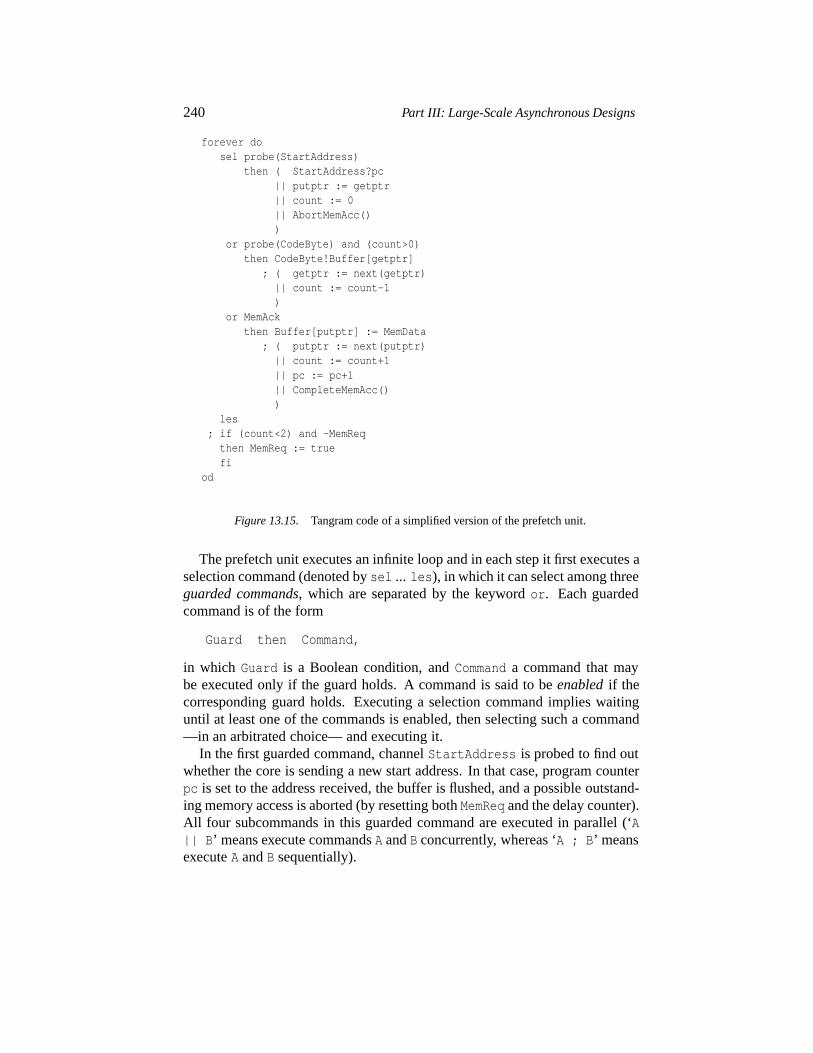
240 Part III: Large-Scale Asynchronous Designs
forever dosel probe(StartAddress)
then ( StartAddress?pc|| putptr := getptr|| count := 0|| AbortMemAcc())
or probe(CodeByte) and (count>0)then CodeByte!Buffer[getptr]
; ( getptr := next(getptr)|| count := count-1)
or MemAckthen Buffer[putptr] := MemData
; ( putptr := next(putptr)|| count := count+1|| pc := pc+1|| CompleteMemAcc())
les; if (count<2) and -MemReq
then MemReq := truefi
od
Figure 13.15. Tangram code of a simplified version of the prefetch unit.
The prefetch unit executes an infinite loop and in each step it first executes aselection command (denoted bysel ... les), in which it can select among threeguarded commands, which are separated by the keywordor. Each guardedcommand is of the form
Guard then Command,
in which Guard is a Boolean condition, andCommand a command that maybe executed only if the guard holds. A command is said to beenabled if thecorresponding guard holds. Executing a selection command implies waitinguntil at least one of the commands is enabled, then selecting such a command—in an arbitrated choice— and executing it.
In the first guarded command, channelStartAddress is probed to find outwhether the core is sending a new start address. In that case, program counterpc is set to the address received, the buffer is flushed, and a possible outstand-ing memory access is aborted (by resetting bothMemReq and the delay counter).All four subcommands in this guarded command are executed in parallel (‘A|| B’ means execute commandsA andB concurrently, whereas ‘A ; B’ meansexecuteA andB sequentially).
Chapter 13: Descale 241
The second guarded command takes care of sending the next program bytevia channelCodeByte to the core if the core is ready to receive that byte andthe buffer is not empty. The third guarded command gets enabled ifMemAckgoes high indicating that the data signals in a read access are valid. In thatcase the value read from memory is put in the buffer after which the memoryhandshake is completed.
After each event, if the buffer is not full and no memory access is beingperformed a next memory access is started. Since(count<2) � -MemReq isan invariant of the loop, the last (conditional) command in the loop can besimplified to unconditional assignmentMemReq:= (count<2).
Note that the value(pc-count) is equal to the program counter in the core,since it is set to the destination address in the case of a jump, increased by1 if a code byte is transferred to the core, and kept invariant if a code byteis read from memory. Therefore the core does not need to hold the programcounter and instead, when the information is needed for a relative branch, it canretrieve the counter value from the prefetch unit. Clearly, this feature requiresan extension of the Tangram code shown in Fig. 13.15.
13.5.3 The DES coprocessor
A transaction may need up to ten single DES conversions, where each con-version takes about 10 ms if it is executed in software. Therefore a hardwaresolution is needed, since these conversions would otherwise consume abouthalf of the transaction time.
Fig. 13.16 shows the datapath of the DES coprocessor. The processor sup-ports both single- and triple-DES conversions and, for the latter type of con-version, contains two keys: a foreground and a background key. Single-DESconversions use the foreground key, whereas triple-DES conversions use theforeground key for the first and third conversion and the background key forthe second conversion. The foreground key is stored in registerCD0 consistingof 56 flipflops (the DES key size is 56 bits), whereas the background key re-sides in variableCD1 consisting of 56 latches. The text value resides in variableLR consisting of 64 latches (DES words contain 64 bits).
A single-DES conversion consists of 16 steps and, in each step, the key ispermuted and a new text value is computed from the old text value and the key.In order to have the key return to its original value at the end of a conversion,the key makes two basic permutations in 12 of the 16 steps and only one inthe remaining 4, where 28 basic permutations are needed for a complete cycle.The permutations are performed in flipflop registerCD0.
Most of the area is taken by the combinational circuit calledDES. Since thiscircuit is also dominant in power dissipation, one should minimize the numberof transitions at its inputs. For this purpose, we have introduced two latch
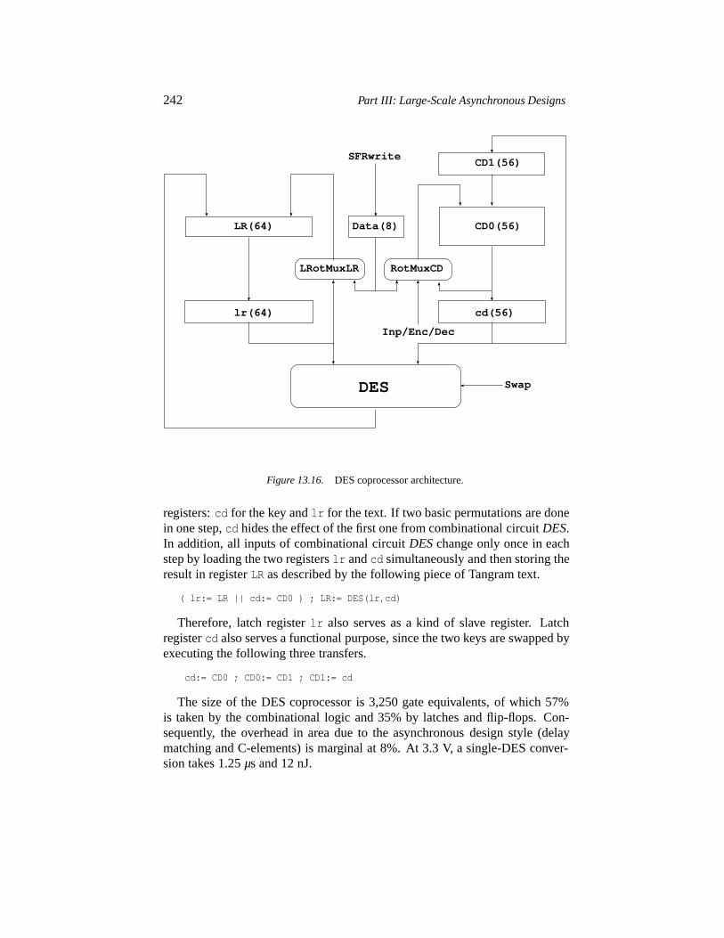
242 Part III: Large-Scale Asynchronous Designs
cd(56)
CD0(56)
CD1(56)
LR(64)
lr(64)
Data(8)
DES
LRotMuxLR RotMuxCD
Swap
Inp/Enc/Dec
SFRwrite
Figure 13.16. DES coprocessor architecture.
registers:cd for the key andlr for the text. If two basic permutations are donein one step,cd hides the effect of the first one from combinational circuitDES.In addition, all inputs of combinational circuitDES change only once in eachstep by loading the two registerslr andcd simultaneously and then storing theresult in registerLR as described by the following piece of Tangram text.
( lr:= LR || cd:= CD0 ) ; LR:= DES(lr,cd)
Therefore, latch registerlr also serves as a kind of slave register. Latchregistercd also serves a functional purpose, since the two keys are swapped byexecuting the following three transfers.
cd:= CD0 ; CD0:= CD1 ; CD1:= cd
The size of the DES coprocessor is 3,250 gate equivalents, of which 57%is taken by the combinational logic and 35% by latches and flip-flops. Con-sequently, the overhead in area due to the asynchronous design style (delaymatching and C-elements) is marginal at 8%. At 3.3 V, a single-DES conver-sion takes 1.25µs and 12 nJ.
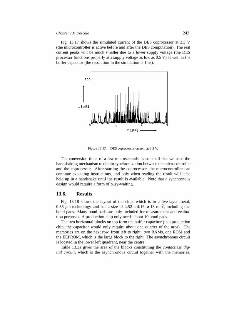
Chapter 13: Descale 243
Fig. 13.17 shows the simulated current of the DES coprocessor at 3.3 V(the microcontroller is active before and after the DES computation). The realcurrent peaks will be much smaller due to a lower supply voltage (the DESprocessor functions properly at a supply voltage as low as 0.5 V) as well as thebuffer capacitor (the resolution in the simulation is 1 ns).
1
100
320
t[µs]
i[mA]
Figure 13.17. DES coprocessor current at 3.3 V.
The conversion time, of a few microseconds, is so small that we used thehandshaking mechanism to obtain synchronization between the microcontrollerand the coprocessor. After starting the coprocessor, the microcontroller cancontinue executing instructions, and only when reading the result will it beheld up in a handshake until the result is available. Note that a synchronousdesign would require a form of busy-waiting.
13.6. Results
Fig. 13.18 shows the layout of the chip, which is in a five-layer metal,0.35 µm technology and has a size of 4�52�4�16 18 mm2, including thebond pads. Many bond pads are only included for measurement and evalua-tion purposes. A production chip only needs about 10 bond pads.
The two horizontal blocks on top form the buffer capacitor (in a productionchip, the capacitor would only require about one quarter of the area). Thememories are on the next row, from left to right: two RAMs, one ROM andthe EEPROM, which is the large block to the right. The asynchronous circuitis located in the lower left quadrant, near the centre.
Table 13.3a gives the area of the blocks constituting thecontactless dig-ital circuit, which is the asynchronous circuit together with the memories.
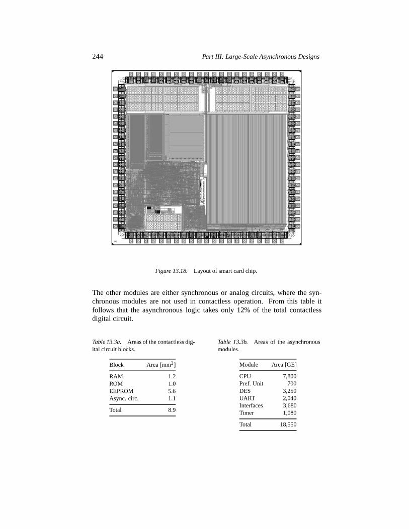
244 Part III: Large-Scale Asynchronous Designs
Figure 13.18. Layout of smart card chip.
The other modules are either synchronous or analog circuits, where the syn-chronous modules are not used in contactless operation. From this table itfollows that the asynchronous logic takes only 12% of the total contactlessdigital circuit.
Table 13.3a. Areas of the contactless dig-ital circuit blocks.
Block Area [mm2]
RAM 1.2ROM 1.0EEPROM 5.6Async. circ. 1.1
Total 8.9
Table 13.3b. Areas of the asynchronousmodules.
Module Area [GE]
CPU 7,800Pref. Unit 700DES 3,250UART 2,040Interfaces 3,680Timer 1,080
Total 18,550
Chapter 13: Descale 245
The sizes of the different asynchronous modules are given in Table 13.3b.In the standard cell library used, a gate equivalent (GE) is 54µm2 with a typicallayout density of 17,500 gates per mm2.
Table 13.3c. Power of the contactlessdigital circuit.
Block Power
Core 56%ROM 27%RAM 17%
Table 13.3d. Effect of asynchronous de-sign on power and area at different levels.
Level Power Area
Async. circ. �70% �18%Async. + Mem. �60% �2%
Table 13.3c shows the power dissipation of the digital circuit blocks whenthe controller is executing code from ROM (being the normal situation).
Table 13.3d shows the effects on power and area of an asynchronous designat two different levels. The asynchronous circuit gives a reduction in powerdissipation of about 70% for 18% additional area. At the level of the contact-less digital circuit, however, we obtain a power reduction of 60% for only 2%additional area. Note that this analysis does not include the synchronous RSAconverter and the analog circuits needed in a production chip, such as for in-stance the buffer capacitor and the power supply unit. Therefore at chip levelthe relative reduction in power dissipation will be about the same, whereas theoverhead in area will be reduced even further.
13.7. Test
The testing of asynchronous circuits for manufacturing defects is known tobe a difficult problem [61, 120]. The main problem is that asynchronous cir-cuits have many feedback loops that cannot be controlled by an external signal.This makes the introduction of scan testing expensive, and forces the designerto become involved in the development of a functional test, either in producingthe patterns directly or in implementing the design-for-test measures.
A functional test approach was chosen for the chip described in this chapter.During test, the microcontroller is connected to an external ROM that containsa test program. This program computes a signature, and a circuit is said to bedefective if the signature is not correct. In addition, current measurements areperformed to increase the test coverage.
The functional tests were developed using the test for the 80C51 microcon-troller [144] as a starting point. Both this test and its extension were developedusing the test-evaluation tool described in [152]. This tool evaluates thestruc-tural test coverage (controllability and observability) offunctional traces.
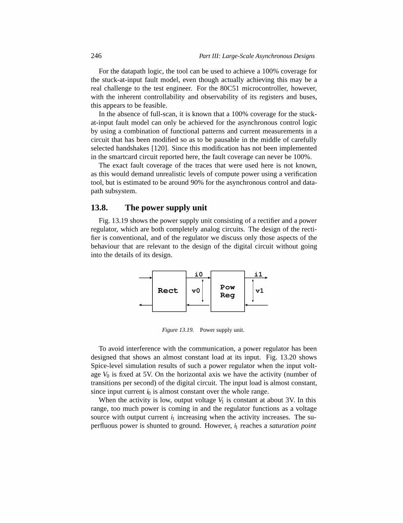
246 Part III: Large-Scale Asynchronous Designs
For the datapath logic, the tool can be used to achieve a 100% coverage forthe stuck-at-input fault model, even though actually achieving this may be areal challenge to the test engineer. For the 80C51 microcontroller, however,with the inherent controllability and observability of its registers and buses,this appears to be feasible.
In the absence of full-scan, it is known that a 100% coverage for the stuck-at-input fault model can only be achieved for the asynchronous control logicby using a combination of functional patterns and current measurements in acircuit that has been modified so as to be pausable in the middle of carefullyselected handshakes [120]. Since this modification has not been implementedin the smartcard circuit reported here, the fault coverage can never be 100%.
The exact fault coverage of the traces that were used here is not known,as this would demand unrealistic levels of compute power using a verificationtool, but is estimated to be around 90% for the asynchronous control and data-path subsystem.
13.8. The power supply unit
Fig. 13.19 shows the power supply unit consisting of a rectifier and a powerregulator, which are both completely analog circuits. The design of the recti-fier is conventional, and of the regulator we discuss only those aspects of thebehaviour that are relevant to the design of the digital circuit without goinginto the details of its design.
PowReg
i0
v0
i1
v1Rect
Figure 13.19. Power supply unit.
To avoid interference with the communication, a power regulator has beendesigned that shows an almost constant load at its input. Fig. 13.20 showsSpice-level simulation results of such a power regulator when the input volt-ageV0 is fixed at 5V. On the horizontal axis we have the activity (number oftransitions per second) of the digital circuit. The input load is almost constant,since input currenti0 is almost constant over the whole range.
When the activity is low, output voltageV1 is constant at about 3V. In thisrange, too much power is coming in and the regulator functions as a voltagesource with output currenti1 increasing when the activity increases. The su-perfluous power is shunted to ground. However,i1 reaches asaturation point
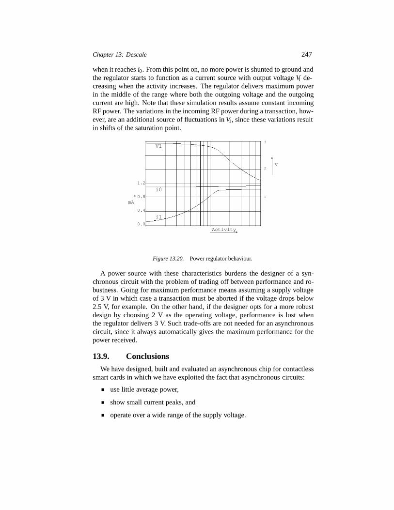
Chapter 13: Descale 247
when it reachesi0. From this point on, no more power is shunted to ground andthe regulator starts to function as a current source with output voltageV1 de-creasing when the activity increases. The regulator delivers maximum powerin the middle of the range where both the outgoing voltage and the outgoingcurrent are high. Note that these simulation results assume constant incomingRF power. The variations in the incoming RF power during a transaction, how-ever, are an additional source of fluctuations inV1, since these variations resultin shifts of the saturation point.
i0
i1
V1
2
3
0.0
0.4
0.8
1.2
mA
V
1
Activity
Figure 13.20. Power regulator behaviour.
A power source with these characteristics burdens the designer of a syn-chronous circuit with the problem of trading off between performance and ro-bustness. Going for maximum performance means assuming a supply voltageof 3 V in which case a transaction must be aborted if the voltage drops below2.5 V, for example. On the other hand, if the designer opts for a more robustdesign by choosing 2 V as the operating voltage, performance is lost whenthe regulator delivers 3 V. Such trade-offs are not needed for an asynchronouscircuit, since it always automatically gives the maximum performance for thepower received.
13.9. Conclusions
We have designed, built and evaluated an asynchronous chip for contactlesssmart cards in which we have exploited the fact that asynchronous circuits:
use little average power,
show small current peaks, and
operate over a wide range of the supply voltage.
248 Part III: Large-Scale Asynchronous Designs
Measurements and simulations showed the following advantages of this de-sign when compared to a conventional synchronous one:
The asynchronous circuit gives the maximum performance for the powerreceived. This comes mainly from the fact that the asynchronous de-sign needs less of what is the main limiting factor for the performance,namely power. Compared to a synchronous design, the asynchronouscircuit needs about 40% of the power for less than 2% additional area.In addition, the automatic speed adaptation property of asynchronouscircuits saves the designer from trading off between performance androbustness. Due to this property the asynchronous circuit will give free-running instead of guaranteed performance, where the difference be-tween the two is about a factor two.
The asynchronous design is more resilient to voltage drops, since it stilloperates correctly for voltages down to 1.5 V.
The current peaks of an asynchronous circuit are less pronounced, mak-ing the requirements with respect to the buffer capacitor more modest.
The combination of the power regulator with the asynchronous circuitgives little communication interference. In this case, the smaller currentpeaks and the self-adaptation property are of importance.
Acknowledgements
We gratefully acknowledge the other members of the Tangram team: Keesvan Berkel, Marc Verra and Erwin Woutersen, and we thank Klaus Ully forhelping us to get the DES converter right.
Chapter 14
AN ASYNCHRONOUS VITERBIDECODER �
Linda E. M. BrackenburyDepartment of Computer Science, The University of Manchester
Abstract Viterbi decoders are used for decoding data encoded using convolutional for-ward error correcting codes. Such codes are used in a large proportion of digitaltransmission and digital recording systems because, even when the transmittedsignal is subjected to significant noise, the decoder is still able efficiently to de-termine the most likely transmitted data.
This chapter descibes a novel Viterbi decoder aimed at being power efficientthrough adopting an asynchronous approach. The new design is based upon se-rial unary arithmetic for the computation and storage of the metrics required;this arithmetic replaces the add-compare-select parallel arithmetic performed byconventional synchronous systems. Like all Viterbi decoders, a history of com-putational results is built up over many data bits to determine the data most likelyto have been transmitted at an earlier time. The identification of a starting pointto this tracing operation allows the storage requirement to be greatly reducedcompared with that in conventional decoders where the starting point is random.Furthermore, asynchronous operation in the system described enables multiple,independent, concurrent tracing operations to be performed which are decoupledfrom the placing of new data in the history memory.
Keywords: low-power asynchronous circuits, Viterbi, convolution decoder
14.1. Introduction
The PREST (Power REduction for Systems Technology) [1] project was acollaborative project where each partner designed a low power alternative to
�The Viterbi design work was supported by the EPSRC/MoD PowerPack project GR/L27930 and the EUPREST project EP25242, and this support is gratefully acknowledged.
249
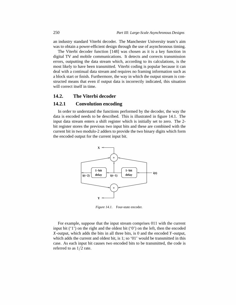
250 Part III: Large-Scale Asynchronous Designs
an industry standard Viterbi decoder. The Manchester University team’s aimwas to obtain a power-efficient design through the use of asynchronous timing.
The Viterbi decoder function [148] was chosen as it is a key function indigital TV and mobile communications. It detects and corrects transmissionerrors, outputting the data stream which, according to its calculations, is themost likely to have been transmitted. Viterbi coding is popular because it candeal with a continual data stream and requires no framing information such asa block start or finish. Furthermore, the way in which the output stream is con-structed means that even if output data is incorrectly indicated, this situationwill correct itself in time.
14.2. The Viterbi decoder
14.2.1 Convolution encoding
In order to understand the functions performed by the decoder, the way thedata is encoded needs to be described. This is illustrated in figure 14.1. Theinput data stream enters a shift register which is initially set to zero. The 2-bit register stores the previous two input bits and these are combined with thecurrent bit in two modulo-2 adders to provide the two binary digits which formthe encoded output for the current input bit.
1−bitdelay
1−bit
+
+
i(t−1)i(t−2)
Y
delay
X
i(t)
Figure 14.1. Four-state encoder.
For example, suppose that the input stream comprises 011 with the currentinput bit (‘1’) on the right and the oldest bit (‘0’) on the left, then the encodedX-output, which adds the bits in all three bits, is 0 and the encodedY -output,which adds the current and oldest bit, is 1; so ‘01’ would be transmitted in thiscase. As each input bit causes two encoded bits to be transmitted, the code isreferred to as 1�2 rate.
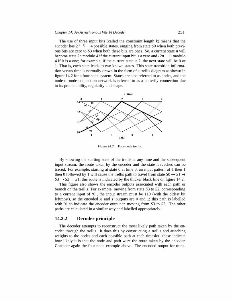
Chapter 14: An Asynchronous Viterbi Decoder 251
The use of three input bits (called the constraint lengthk) means that theencoder has 2�k�1� � 4 possible states, ranging from stateS0 when both previ-ous bits are zero toS3 when both these bits are ones. So, a current staten willbecome state 2n modulo 4 if the current input bit is a zero and�2n�1� modulo4 if it is a one; for example, if the current state is 2, the next state will be 0 or1. That is, each state leads to two known states. This state transition informa-tion versus time is normally drawn in the form of a trellis diagram as shown infigure 14.2 for a four-state system. States are also referred to as nodes, and thenode-to-node connection network is referred to as a butterfly connection dueto its predictability, regularity and shape.
S3
S2
S1
S0
0 1 2 3 4
1 1 0 1
time
00
10
11
01
01
1000
11
data
Figure 14.2. Four-node trellis.
By knowing the starting state of the trellis at any time and the subsequentinput stream, the route taken by the encoder and the state it reaches can betraced. For example, starting at state 0 at time 0, an input pattern of 1 then 1then 0 followed by 1 will cause the trellis path to travel from stateS0� S1�S3� S2� S1; this route is indicated by the thicker black line on figure 14.2.
This figure also shows the encoder outputs associated with each path orbranch on the trellis. For example, moving from stateS3 to S2, correspondingto a current input of ‘0’, the input stream must be 110 (with the oldest bitleftmost), so the encodedX andY outputs are 0 and 1; this path is labelledwith 01 to indicate the encoder output in moving fromS3 to S2. The otherpaths are calculated in a similar way and labelled appropriately.
14.2.2 Decoder principle
The decoder attempts to reconstruct the most likely path taken by the en-coder through the trellis. It does this by constructing a trellis and attachingweights to the nodes and each possible path at each timeslot; these indicatehow likely it is that the node and path were the route taken by the encoder.Consider again the four-node example above. The encoded output for trans-
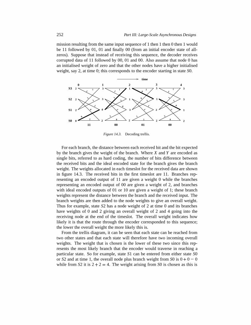
252 Part III: Large-Scale Asynchronous Designs
mission resulting from the same input sequence of 1 then 1 then 0 then 1 wouldbe 11 followed by 01, 01 and finally 00 (from an initial encoder state of all-zeros). Suppose that instead of receiving this sequence, the decoder receivescorrupted data of 11 followed by 00, 01 and 00. Also assume that node 0 hasan initialised weight of zero and that the other nodes have a higher initialisedweight, say 2, at time 0; this corresponds to the encoder starting in stateS0.
S3
S2
S1
S0
2
2
2
0
0
11
1
2
0
1
2
11
2
11
1
02
1
0
00
1
20
0
1
1
2
1
01
3
3
1
2
2
11
1
0
2
1
0
00
3
0
2 2
3
1
1
2
2
210 3 43 3
1
time
Figure 14.3. Decoding trellis.
For each branch, the distance between each received bit and the bit expectedby the branch gives the weight of the branch. WhereX andY are encoded assingle bits, referred to as hard coding, the number of bits difference betweenthe received bits and the ideal encoded state for the branch gives the branchweight. The weights allocated in each timeslot for the received data are shownin figure 14.3. The received bits in the first timeslot are 11. Branches rep-resenting an encoded output of 11 are given a weight 0 while the branchesrepresenting an encoded output of 00 are given a weight of 2, and brancheswith ideal encoded outputs of 01 or 10 are given a weight of 1; these branchweights represent the distance between the branch and the received input. Thebranch weights are then added to the node weights to give an overall weight.Thus for example, stateS2 has a node weight of 2 at time 0 and its brancheshave weights of 0 and 2 giving an overall weight of 2 and 4 going into thereceiving node at the end of the timeslot. The overall weight indicates howlikely it is that the route through the encoder corresponded to this sequence;the lower the overall weight the more likely this is.
From the trellis diagram, it can be seen that each state can be reached fromtwo other states and that each state will therefore have two incoming overallweights. The weight that is chosen is the lower of these two since this rep-resents the most likely branch that the encoder would traverse in reaching aparticular state. So for example, stateS1 can be entered from either stateS0or S2 and at time 1, the overall node plus branch weight fromS0 is 0�0� 0while from S2 it is 2�2� 4. The weight arising fromS0 is chosen as this is
Chapter 14: An Asynchronous Viterbi Decoder 253
the lower and therefore more likely route intoS1; the weight arising from theS2 branch is discarded and the new weight for nodeS1 at the end of this firsttimeslot is that fromS0, i.e. 0.
This process continues in a similar way for each timeslot with weights givento each branch according to the difference between the encoded branch patternand the received bits. This difference is then added to the node weight to givean overall weight with the next weight for a node equal to the lower incomingweight. This results in the weights given in figure 14.3.
To form the output from the decoder, a path is traced through its trellis usingthe accumulated history of node weight information. The weights at time 4indicate that the encoder is most likely to be in stateS1 as this has the lowestnode weight. Furthermore, this state was most likely to have been reachedfrom S2. Continuing tracing backwards fromS2 taking the lower overall nodecount, the most likely path taken fromS2 isS3, S1 andS0 (initialisation). Notethat despite having received corrupted data, this is exactly the sequence takenby the encoder in sending this data!
The output data can be ‘rescued’ from the decoder by noting that to reachstatesS0 andS2 the current data input to the encoder is a ‘0’ while to reachstatesS1 andS3, the current encoder input is a ‘1’; that is, the least significantstate bit indicates the state of the current data. Thus since the optimum statesthe decoder reaches at time 1, 2, 3 and 4 isS1, S3, S2 andS1 respectively, thedecoder would output a data stream of 1101 as being the most likely input tothe encoder.
14.3. System parameters
In practice the decoder designed is larger and more complicated than indi-cated by the simple example given. The encoder uses the current bit and thesix previous bits in various combinations to provide the two encoded outputstreams; this spreads each input bit out over a longer transmission period, in-creasing the probability of error-free reception in the presence of noise. If thecurrent bit is bit 0 with the oldest bit in the shift register being bit 6, then theencodedX-output is obtained by adding bits 0, 1, 2, 3 and 6 and the encodedY -output from adding bits 0, 2, 3, 5 and 6. Since the constraint length is 7, thesystem has 64 nodes and therefore 128 paths or branches. Thus staten, wheren is an integer from 0 to 63, leads to states 2n modulo 64 and�2n�1� modulo64.
Furthermore, the received bits are not hard coded (just straight ones andzeros) but soft coded. Three bits are used to represent values, with 100 usedfor a strong zero value and 011 for a strong one value. Noise in transmissionmeans that a received character can be indicated by any 3-bit value from 0 to7 and in interpreting the received value, it is helpful to regard the number as
254 Part III: Large-Scale Asynchronous Designs
signed. Thus 011 indicates a strong one while 000 denotes received data thatweakly indicates a one. Similarly, 100 implies a strong zero while 111 denotesa probable but weak zero. To make the text easier to follow hereafter, unsignedvalues will be used with the code for a 3-bit perfect zero taken as 000 (i.e.value 0) while a 3-bit perfect one is taken as 111 (i.e. value 7).
The interface to the asynchrous decoder is synchronous with the validity ofthe encoded characters on a particular positive clock edge indicated by a Block-Valid signal; encoded data is only present when this signal is high. Code ratesother than the 1/2, primarily described in this chapter, are also possible. Theseare achieved by using the Block-Valid with a Puncture and a Puncture-X-nYsignal; if Block-Valid is active (high) then a high Puncture signal indicates thatonly one of theX or Y symbols is valid and Puncture-X-nY indicates which.Both encoded characters are present if Block-Valid is high and Puncture is low.All the code rates originate from the 1/2 rate encoder with data for the othercode rates then obtained by omitting to send some of these encoded characters.In this way, in addition to the 1/2 code rate, the system receives and decodesrates of 2/3 (two input bits result in the transmission of three encoded charac-ters), 3/4, 5/6, 6/7 and 7/8 (7 input bits defined by 8 encoded characters withthe remaining 6 not transmitted). As the code rate progressively increases, lessredundancy is included in the transmitted data resulting in an increased errorrate from the decoder; a rate of 1/2 will yield the most error-free output.
The system is expected to be operated from a 90 MHz clock. Since thisclock is used by all code rates, the code rate not only defines the ratio of thenumber of input bits to the number of transmitted encoded characters but alsospecifies the ratio of the number of clocks containing encoded information (of1 or 2 valid characters) to the number of clock cycles. For example, a 3/4 ratesignifies that three input bits result in four transmitted characters and also thatthree clocks out of four contain some encoded information. Thus in a 3/4 code,every fourth clock contains no encoded information (Block-Valid is low). Anyclock for which Block-Valid is high is said to contain a symbol. Thus witha 90 MHz clock rate, a 1/2 rate code which has valid data on alternate clockcycles yields a data rate of 45 MSymbols/sec and a 7/8 code rate is equivalentto 90x7/8 Msymbols/sec = 78.75 Msymbols/sec.
14.4. System overview
To perform the decoder computation previously outlined, the Viterbi de-coder comprises three units as shown in figure 14.4. The Branch Metric Unit(BMU) receives the transmitted data and computes the distance between theideal branch pattern symbols of (0,0), (0,7), (7,0) or (7,7) and the receiveddata; these weights are then passed to the Path Metric Unit (PMU). The PMUholds the node weights and performs the node plus branch weight calculations,
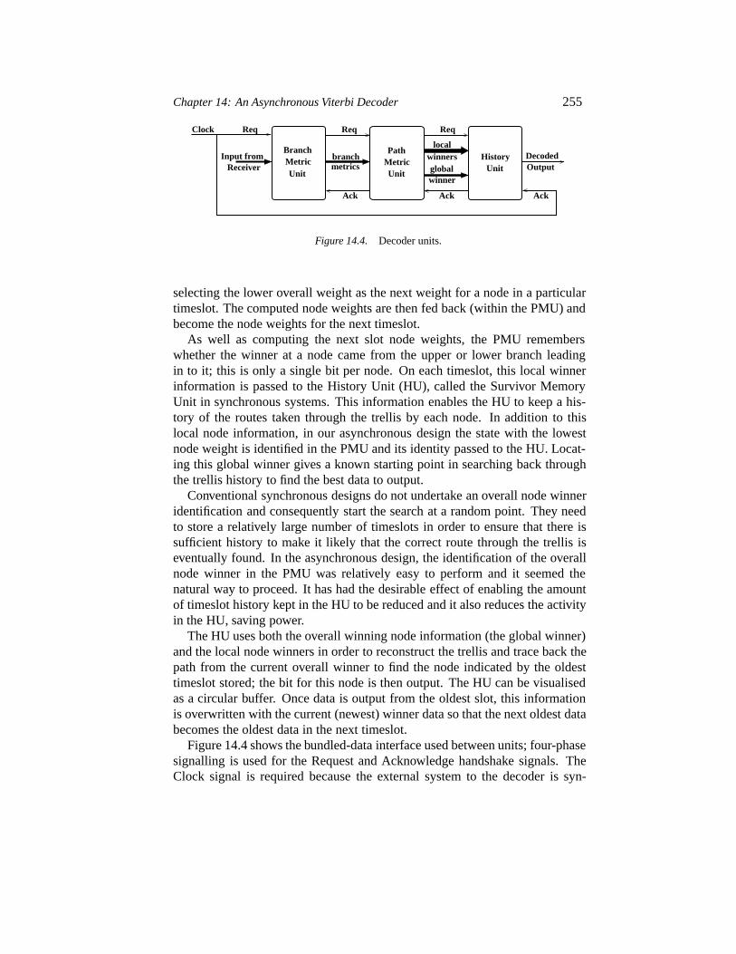
Chapter 14: An Asynchronous Viterbi Decoder 255
Clock Req Req
branch
Ack
Req
UnitHistory
globalMetricPath
UnitMetricUnit
Branch
Receiver
Ack
DecodedOutput
Ack
winner
Input frommetrics
localwinners
Figure 14.4. Decoder units.
selecting the lower overall weight as the next weight for a node in a particulartimeslot. The computed node weights are then fed back (within the PMU) andbecome the node weights for the next timeslot.
As well as computing the next slot node weights, the PMU rememberswhether the winner at a node came from the upper or lower branch leadingin to it; this is only a single bit per node. On each timeslot, this local winnerinformation is passed to the History Unit (HU), called the Survivor MemoryUnit in synchronous systems. This information enables the HU to keep a his-tory of the routes taken through the trellis by each node. In addition to thislocal node information, in our asynchronous design the state with the lowestnode weight is identified in the PMU and its identity passed to the HU. Locat-ing this global winner gives a known starting point in searching back throughthe trellis history to find the best data to output.
Conventional synchronous designs do not undertake an overall node winneridentification and consequently start the search at a random point. They needto store a relatively large number of timeslots in order to ensure that there issufficient history to make it likely that the correct route through the trellis iseventually found. In the asynchronous design, the identification of the overallnode winner in the PMU was relatively easy to perform and it seemed thenatural way to proceed. It has had the desirable effect of enabling the amountof timeslot history kept in the HU to be reduced and it also reduces the activityin the HU, saving power.
The HU uses both the overall winning node information (the global winner)and the local node winners in order to reconstruct the trellis and trace back thepath from the current overall winner to find the node indicated by the oldesttimeslot stored; the bit for this node is then output. The HU can be visualisedas a circular buffer. Once data is output from the oldest slot, this informationis overwritten with the current (newest) winner data so that the next oldest databecomes the oldest data in the next timeslot.
Figure 14.4 shows the bundled-data interface used between units; four-phasesignalling is used for the Request and Acknowledge handshake signals. TheClock signal is required because the external system to the decoder is syn-
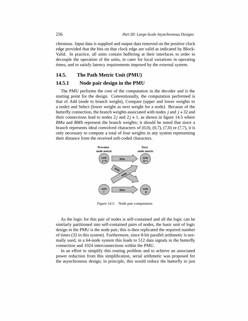
256 Part III: Large-Scale Asynchronous Designs
chronous. Input data is supplied and output data removed on the positive clockedge provided that the bits on that clock edge are valid as indicated by Block-Valid. In practice, all units contain buffering at their interfaces in order todecouple the operation of the units, to cater for local variations in operatingtimes, and to satisfy latency requirements imposed by the external system.
14.5. The Path Metric Unit (PMU)
14.5.1 Node pair design in the PMU
The PMU performs the core of the computation in the decoder and is thestarting point for the design. Conventionally, the computation performed isthat of Add (node to branch weight), Compare (upper and lower weights toa node) and Select (lower weight as next weight for a node). Because of thebutterfly connection, the branch weights associated with nodesj and j�32 andtheir connections lead to nodes 2j and 2j �1, as shown in figure 14.5 whereBMa andBMb represent the branch weights; it should be noted that since abranch represents ideal convolved characters of (0,0), (0,7), (7,0) or (7,7), it isonly necessary to compute a total of four weights in any system representingtheir distance from the received soft-coded characters.
node metricPrevious
node
node
nodenode BMa
BMa
BMb
BMb
Nextnode metric
j+32
j
2j+1
2j
Figure 14.5. Node pair computation.
As the logic for this pair of nodes is self-contained and all the logic can besimilarly partitioned into self-contained pairs of nodes, the basic unit of logicdesign in the PMU is the node pair; this is then replicated the required numberof times (32 in this system). Furthermore, since 8-bit parallel arithmetic is nor-mally used, in a 64-node system this leads to 512 data signals in the butterflyconnection and 1024 interconnections within the PMU.
In an effort to simplify this routing problem and to achieve an associatedpower reduction from this simplification, serial arithmetic was proposed forthe asynchronous design; in principle, this would reduce the butterfly to just
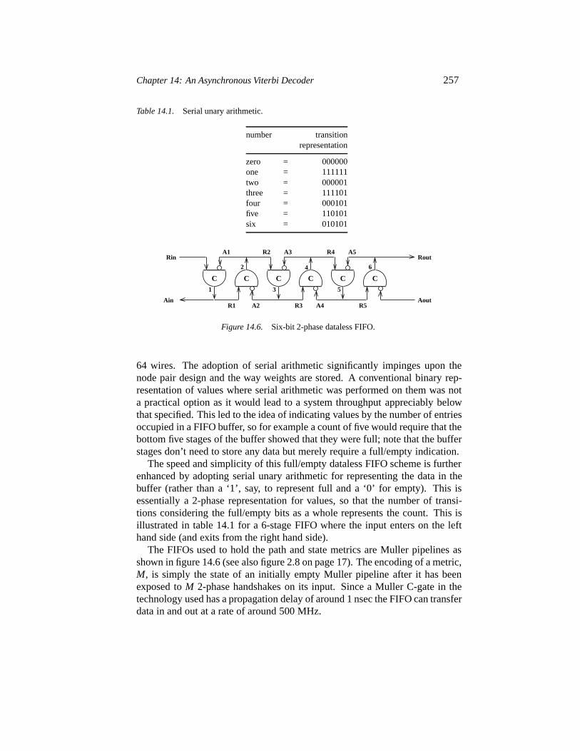
Chapter 14: An Asynchronous Viterbi Decoder 257
Table 14.1. Serial unary arithmetic.
number transitionrepresentation
zero = 000000one = 111111two = 000001three = 111101four = 000101five = 110101six = 010101
Ain
Rin Rout
Aout
C C C C C C
R1
A1 R2
A2 R3 A4
A3 R4 A5
R5
1 3 5
2 4 6
Figure 14.6. Six-bit 2-phase dataless FIFO.
64 wires. The adoption of serial arithmetic significantly impinges upon thenode pair design and the way weights are stored. A conventional binary rep-resentation of values where serial arithmetic was performed on them was nota practical option as it would lead to a system throughput appreciably belowthat specified. This led to the idea of indicating values by the number of entriesoccupied in a FIFO buffer, so for example a count of five would require that thebottom five stages of the buffer showed that they were full; note that the bufferstages don’t need to store any data but merely require a full/empty indication.
The speed and simplicity of this full/empty dataless FIFO scheme is furtherenhanced by adopting serial unary arithmetic for representing the data in thebuffer (rather than a ‘1’, say, to represent full and a ‘0’ for empty). This isessentially a 2-phase representation for values, so that the number of transi-tions considering the full/empty bits as a whole represents the count. This isillustrated in table 14.1 for a 6-stage FIFO where the input enters on the lefthand side (and exits from the right hand side).
The FIFOs used to hold the path and state metrics are Muller pipelines asshown in figure 14.6 (see also figure 2.8 on page 17). The encoding of a metric,M, is simply the state of an initially empty Muller pipeline after it has beenexposed toM 2-phase handshakes on its input. Since a Muller C-gate in thetechnology used has a propagation delay of around 1 nsec the FIFO can transferdata in and out at a rate of around 500 MHz.
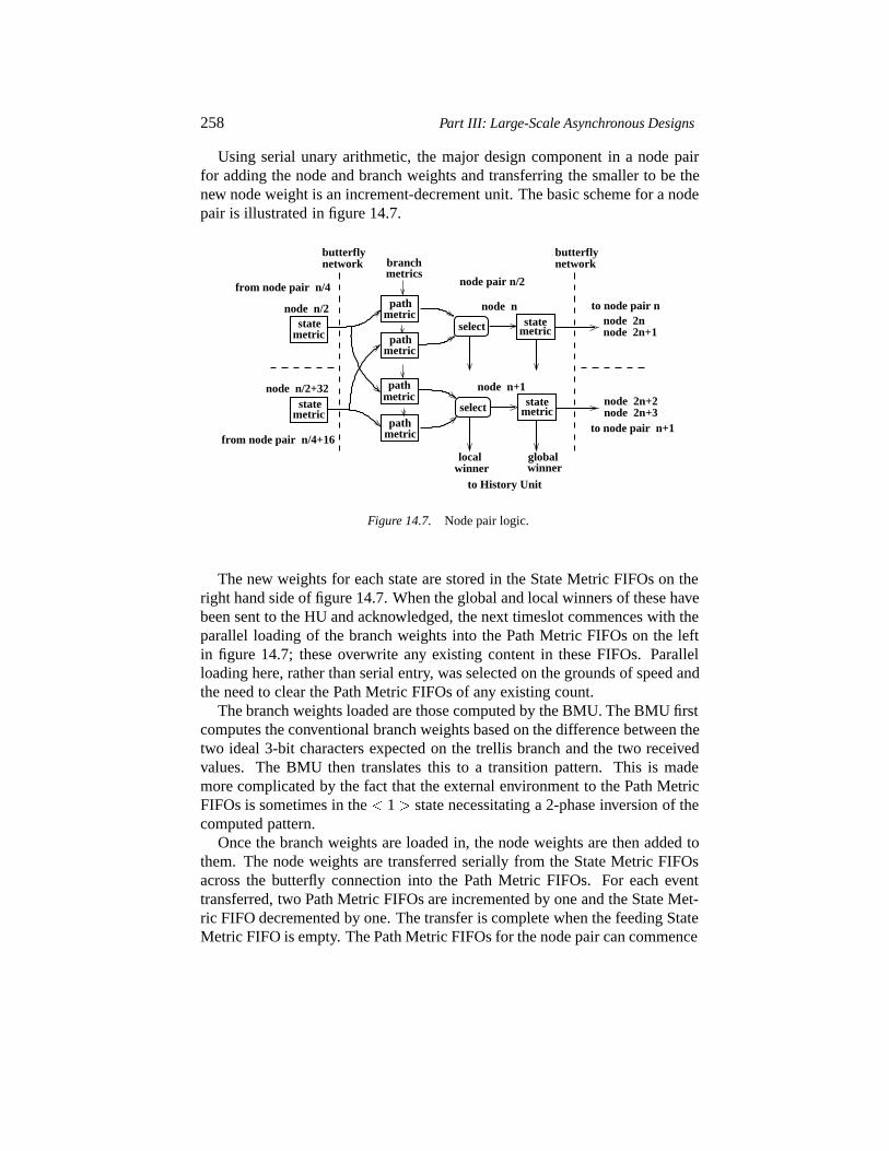
258 Part III: Large-Scale Asynchronous Designs
Using serial unary arithmetic, the major design component in a node pairfor adding the node and branch weights and transferring the smaller to be thenew node weight is an increment-decrement unit. The basic scheme for a nodepair is illustrated in figure 14.7.
node 2n+1node 2n
node 2n+3node 2n+2
node n/2
node n/2+32
from node pair n/4
from node pair n/4+16to node pair n+1
to node pair n
butterflynetwork
butterflynetwork
metricstate
statemetric
path
metricsbranch
path
path
path
global
statemetric
statemetric
localwinner
metric
metric
metric
select
select
node n+1
node n
node pair n/2
winner
to History Unit
metric
Figure 14.7. Node pair logic.
The new weights for each state are stored in the State Metric FIFOs on theright hand side of figure 14.7. When the global and local winners of these havebeen sent to the HU and acknowledged, the next timeslot commences with theparallel loading of the branch weights into the Path Metric FIFOs on the leftin figure 14.7; these overwrite any existing content in these FIFOs. Parallelloading here, rather than serial entry, was selected on the grounds of speed andthe need to clear the Path Metric FIFOs of any existing count.
The branch weights loaded are those computed by the BMU. The BMU firstcomputes the conventional branch weights based on the difference between thetwo ideal 3-bit characters expected on the trellis branch and the two receivedvalues. The BMU then translates this to a transition pattern. This is mademore complicated by the fact that the external environment to the Path MetricFIFOs is sometimes in the� 1� state necessitating a 2-phase inversion of thecomputed pattern.
Once the branch weights are loaded in, the node weights are then added tothem. The node weights are transferred serially from the State Metric FIFOsacross the butterfly connection into the Path Metric FIFOs. For each eventtransferred, two Path Metric FIFOs are incremented by one and the State Met-ric FIFO decremented by one. The transfer is complete when the feeding StateMetric FIFO is empty. The Path Metric FIFOs for the node pair can commence
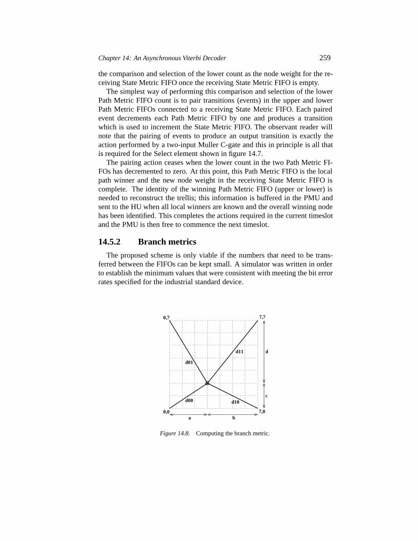
Chapter 14: An Asynchronous Viterbi Decoder 259
the comparison and selection of the lower count as the node weight for the re-ceiving State Metric FIFO once the receiving State Metric FIFO is empty.
The simplest way of performing this comparison and selection of the lowerPath Metric FIFO count is to pair transitions (events) in the upper and lowerPath Metric FIFOs connected to a receiving State Metric FIFO. Each pairedevent decrements each Path Metric FIFO by one and produces a transitionwhich is used to increment the State Metric FIFO. The observant reader willnote that the pairing of events to produce an output transition is exactly theaction performed by a two-input Muller C-gate and this in principle is all thatis required for the Select element shown in figure 14.7.
The pairing action ceases when the lower count in the two Path Metric FI-FOs has decremented to zero. At this point, this Path Metric FIFO is the localpath winner and the new node weight in the receiving State Metric FIFO iscomplete. The identity of the winning Path Metric FIFO (upper or lower) isneeded to reconstruct the trellis; this information is buffered in the PMU andsent to the HU when all local winners are known and the overall winning nodehas been identified. This completes the actions required in the current timeslotand the PMU is then free to commence the next timeslot.
14.5.2 Branch metrics
The proposed scheme is only viable if the numbers that need to be trans-ferred between the FIFOs can be kept small. A simulator was written in orderto establish the minimum values that were consistent with meeting the bit errorrates specified for the industrial standard device.
����
7,7
d
a b
d11
d00c
d01
d10
7,00,0
0,7
Figure 14.8. Computing the branch metric.
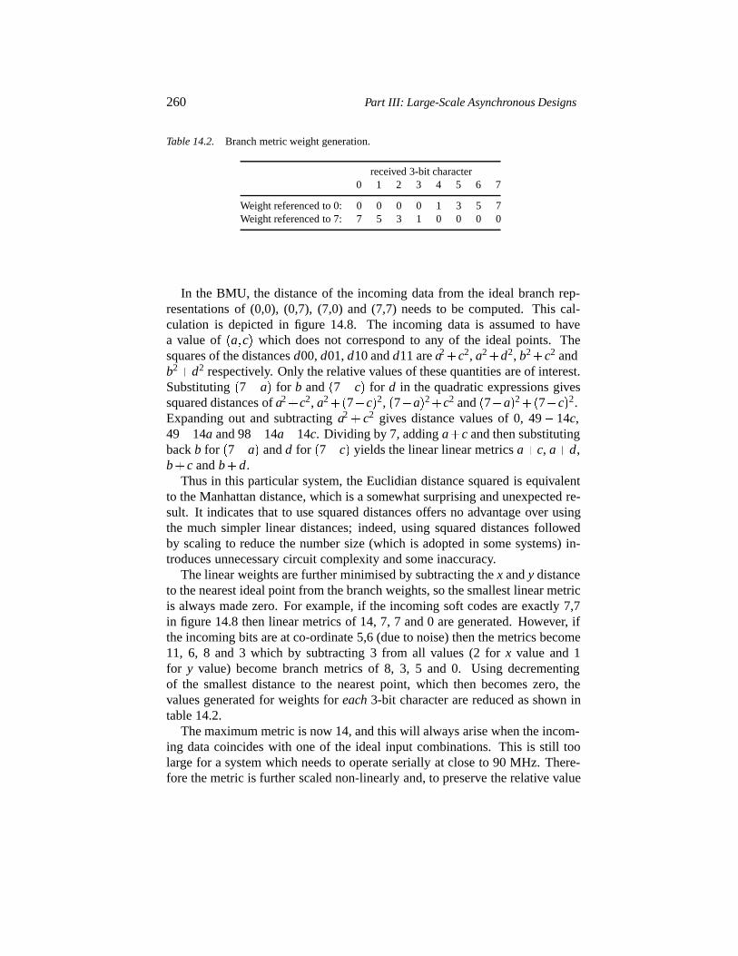
260 Part III: Large-Scale Asynchronous Designs
Table 14.2. Branch metric weight generation.
received 3-bit character0 1 2 3 4 5 6 7
Weight referenced to 0: 0 0 0 0 1 3 5 7Weight referenced to 7: 7 5 3 1 0 0 0 0
In the BMU, the distance of the incoming data from the ideal branch rep-resentations of (0,0), (0,7), (7,0) and (7,7) needs to be computed. This cal-culation is depicted in figure 14.8. The incoming data is assumed to havea value of�a�c� which does not correspond to any of the ideal points. Thesquares of the distancesd00,d01,d10 andd11 area2�c2, a2�d2, b2�c2 andb2�d2 respectively. Only the relative values of these quantities are of interest.Substituting�7� a� for b and�7� c� for d in the quadratic expressions givessquared distances ofa2�c2, a2��7�c�2, �7�a�2�c2 and�7�a�2��7�c�2.Expanding out and subtractinga2 � c2 gives distance values of 0, 49�14c,49�14a and 98�14a�14c. Dividing by 7, addinga�c and then substitutingbackb for �7�a� andd for �7�c� yields the linear linear metricsa�c, a�d,b� c andb�d.
Thus in this particular system, the Euclidian distance squared is equivalentto the Manhattan distance, which is a somewhat surprising and unexpected re-sult. It indicates that to use squared distances offers no advantage over usingthe much simpler linear distances; indeed, using squared distances followedby scaling to reduce the number size (which is adopted in some systems) in-troduces unnecessary circuit complexity and some inaccuracy.
The linear weights are further minimised by subtracting thex andy distanceto the nearest ideal point from the branch weights, so the smallest linear metricis always made zero. For example, if the incoming soft codes are exactly 7,7in figure 14.8 then linear metrics of 14, 7, 7 and 0 are generated. However, ifthe incoming bits are at co-ordinate 5,6 (due to noise) then the metrics become11, 6, 8 and 3 which by subtracting 3 from all values (2 forx value and 1for y value) become branch metrics of 8, 3, 5 and 0. Using decrementingof the smallest distance to the nearest point, which then becomes zero, thevalues generated for weights foreach 3-bit character are reduced as shown intable 14.2.
The maximum metric is now 14, and this will always arise when the incom-ing data coincides with one of the ideal input combinations. This is still toolarge for a system which needs to operate serially at close to 90 MHz. There-fore the metric is further scaled non-linearly and, to preserve the relative value
Chapter 14: An Asynchronous Viterbi Decoder 261
of the weights, this is performed separately on each of the two incoming 3-bitsoft values.
Referring to table 14.2, weights of zero remain zero while weights of 1, 3, 5and 7 are scaled to 1, 2, 3 and 4. Clearly, the weights for both 3-bit soft codesneed to be added to obtain the overall branch metric weight. Thus for example,the incoming soft-codes of 7,7 generate weights of 4+4, 4+0, 0+4 and 0 = 8, 4,4 and 0, while incoming soft-codes of 5,6 generates weights of 2+3, 2+0, 0+3and 0 = 5, 2, 3 and 0. Although the scaling here is non-linear and will thereforeintroduce some inaccuracy, simulation showed that this was not significant inrelation to the results obtained with and without the scaling.
Furthermore, simulation also reveals that, unsurprisingly, paths with thelargest weights are rarely involved in the most likely path to be chosen dur-ing the path reconstruction to find the output. Therefore, weights generatedcan be limited or capped and a limit of 6 is used in the BMU. Thus the weightsactually generated and loaded by the BMU for a 7,7 soft code input are 6, 4, 4and 0; however, the weights for a 5,6 input code remain as above.
Six-bit FIFOs are used throughout the PMU and again numbers in the PMUare capped at 6. To deal with cases where the serial addition of the node metricto a branch weight would exceed this number, logic referred to as the OverflowUnit is placed at the input of each Path Metric FIFO. This receives the incom-ing request handshake but does not pass it to the FIFO, instead it returns it tothe sending State Metric FIFO as an acknowledge signal.
14.5.3 Slot timing
The overall or global winner from the PMU in a particular timeslot is thenode having the lowest state metric count. In the same way that the BMUvalues can be adjusted so that the lowest weight is zero, the state metric valuescan also be decremented so that their minimum value is zero. As a result,numbers in the BMU and PMU are guaranteed to range only between zero andsix. Furthermore if the soft bits contain no noise, which is the situation most ofthe time, then one (and only one) State Metric FIFO will contain a zero countindicating the best path through the trellis. This means that in the majority oftimeslots, there is no need to perform any subtraction on the state metrics.
Detecting that a count is zero is in itself easy since it is indicated by an all-zeros state in the FIFO. This, as well as establishing the local winner, is donelocally within a node and is timed from the control signals applied to the node;each node has a control section which generates the timing signals required bythe node, and the timing within a node is independent of the timing of all othernodes.
A slot commences with the loading of the BMU branch weights. The nodetiming then passes to the next stage where the state-to-path metric transfer is
262 Part III: Large-Scale Asynchronous Designs
performed. Following this, detecting that the sending State Metric FIFOs andthe State Metric FIFO to receive the lower path metric count are empty causesthe generation of a state-to-path metric done signal. The node timing thenmoves on to the next phase which generates a path-to-state metric enable. Ifat the time this signal is activated one of the Path Metric FIFOs for the nodeis empty, then a flip-flop is set indicating that this node is a global winnercandidate; in this case no transfer to the State Metric FIFO is required andthe path-to-state metric done signal is generated; this signal is used to clockthe upper/lower branch (local) winner into a flip-flop and also to set a ‘localwinner found’ flip-flop.
If neither Path Metric FIFO is empty then the path-to-state enable signalallows the transfer to its State Metric FIFO until one of the Path Metric FIFOsbecomes empty; at this point, the path-to-state metric done signal is generated,setting the ‘local winner’ and the ‘local winner found’ flip-flops only.
The ‘local winner found’ and ‘global winner found’ signals now progressup the PMU logic hierarchy to the top level because all information neededto be passed to the HU has to be present before the request out signal to theHU is generated by the PMU. Furthermore, when the local and global winnerdata have been assembled for the HU, all nodes need to be informed that theslot has ended and the timing can be shifted to the start of the next slot. Itshould therefore be noted that while the timing within the nodes is local, thecommunication of the winner information to the HU and the subsequent releaseof the nodes has to be global.
14.5.4 Global winner identification
The formation of the ‘all local winners found’ and the global winner identi-fication is partitioned across the various levels of the PMU logic hierarchy. Atthe level of a pair of node pairs, the four global winner candidate signals areinput to a priority function which produces a 2-bit node address and a ‘globalwinner found’ signal if one of the inputs was a candidate. This logic is repeatedwith four such pairs of node pairs so that using the ‘global winner found’ sig-nal generated by each pair of node pairs, the two bit address obtained indicateswhich pair of node pairs contains the global winner; these are then combinedwith the two-bit address generated by that pair of node pairs to form a 4-bitnode address. Finally, this logic is repeated at the top level where there arefour sets of four pairs of node pairs. Again the ‘global winner found’ signalfrom each set is used in a priority logic function to produce the two-bit addressof the winning set and this is combined with the four address bits identifyingthe winning node within the winning set; this is the 6-bit node identificationthat is sent to the HU as the global winner.
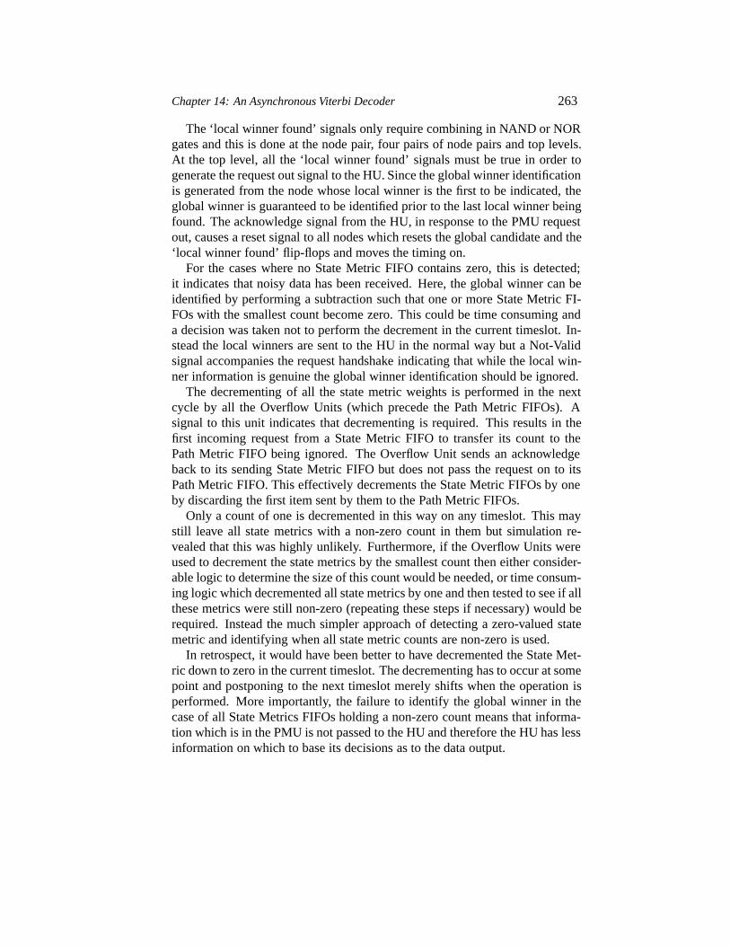
Chapter 14: An Asynchronous Viterbi Decoder 263
The ‘local winner found’ signals only require combining in NAND or NORgates and this is done at the node pair, four pairs of node pairs and top levels.At the top level, all the ‘local winner found’ signals must be true in order togenerate the request out signal to the HU. Since the global winner identificationis generated from the node whose local winner is the first to be indicated, theglobal winner is guaranteed to be identified prior to the last local winner beingfound. The acknowledge signal from the HU, in response to the PMU requestout, causes a reset signal to all nodes which resets the global candidate and the‘local winner found’ flip-flops and moves the timing on.
For the cases where no State Metric FIFO contains zero, this is detected;it indicates that noisy data has been received. Here, the global winner can beidentified by performing a subtraction such that one or more State Metric FI-FOs with the smallest count become zero. This could be time consuming anda decision was taken not to perform the decrement in the current timeslot. In-stead the local winners are sent to the HU in the normal way but a Not-Validsignal accompanies the request handshake indicating that while the local win-ner information is genuine the global winner identification should be ignored.
The decrementing of all the state metric weights is performed in the nextcycle by all the Overflow Units (which precede the Path Metric FIFOs). Asignal to this unit indicates that decrementing is required. This results in thefirst incoming request from a State Metric FIFO to transfer its count to thePath Metric FIFO being ignored. The Overflow Unit sends an acknowledgeback to its sending State Metric FIFO but does not pass the request on to itsPath Metric FIFO. This effectively decrements the State Metric FIFOs by oneby discarding the first item sent by them to the Path Metric FIFOs.
Only a count of one is decremented in this way on any timeslot. This maystill leave all state metrics with a non-zero count in them but simulation re-vealed that this was highly unlikely. Furthermore, if the Overflow Units wereused to decrement the state metrics by the smallest count then either consider-able logic to determine the size of this count would be needed, or time consum-ing logic which decremented all state metrics by one and then tested to see if allthese metrics were still non-zero (repeating these steps if necessary) would berequired. Instead the much simpler approach of detecting a zero-valued statemetric and identifying when all state metric counts are non-zero is used.
In retrospect, it would have been better to have decremented the State Met-ric down to zero in the current timeslot. The decrementing has to occur at somepoint and postponing to the next timeslot merely shifts when the operation isperformed. More importantly, the failure to identify the global winner in thecase of all State Metrics FIFOs holding a non-zero count means that informa-tion which is in the PMU is not passed to the HU and therefore the HU has lessinformation on which to base its decisions as to the data output.
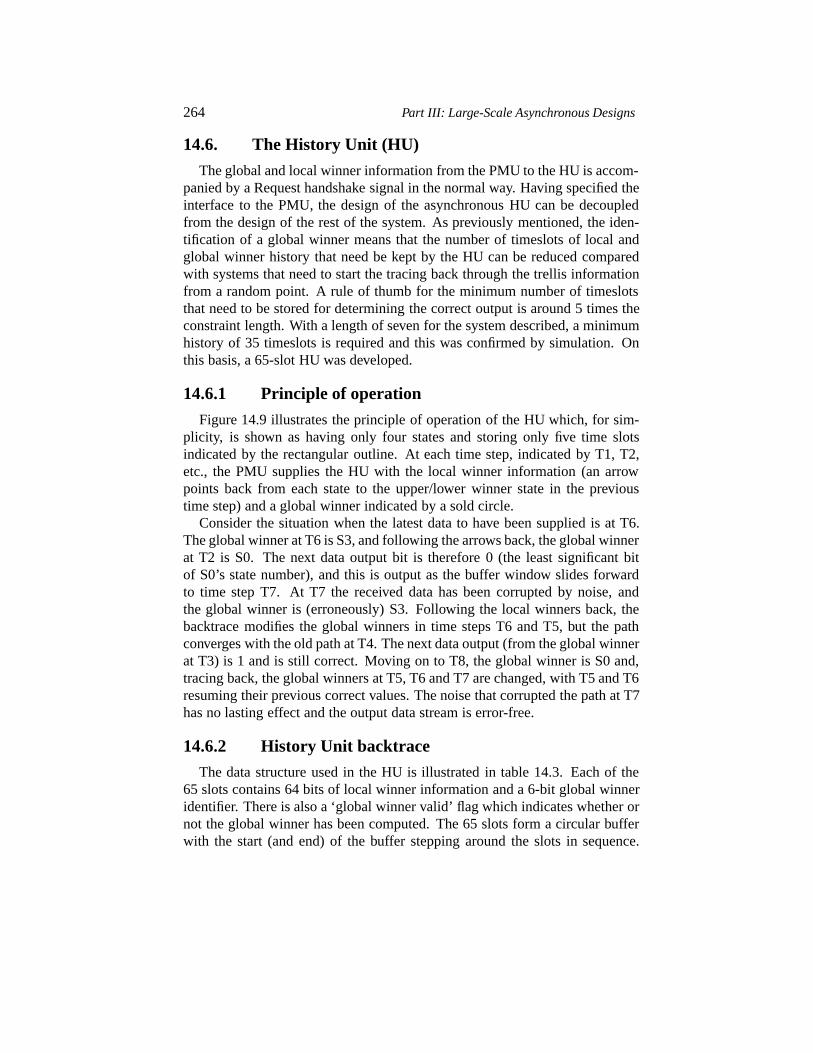
264 Part III: Large-Scale Asynchronous Designs
14.6. The History Unit (HU)
The global and local winner information from the PMU to the HU is accom-panied by a Request handshake signal in the normal way. Having specified theinterface to the PMU, the design of the asynchronous HU can be decoupledfrom the design of the rest of the system. As previously mentioned, the iden-tification of a global winner means that the number of timeslots of local andglobal winner history that need be kept by the HU can be reduced comparedwith systems that need to start the tracing back through the trellis informationfrom a random point. A rule of thumb for the minimum number of timeslotsthat need to be stored for determining the correct output is around 5 times theconstraint length. With a length of seven for the system described, a minimumhistory of 35 timeslots is required and this was confirmed by simulation. Onthis basis, a 65-slot HU was developed.
14.6.1 Principle of operation
Figure 14.9 illustrates the principle of operation of the HU which, for sim-plicity, is shown as having only four states and storing only five time slotsindicated by the rectangular outline. At each time step, indicated by T1, T2,etc., the PMU supplies the HU with the local winner information (an arrowpoints back from each state to the upper/lower winner state in the previoustime step) and a global winner indicated by a sold circle.
Consider the situation when the latest data to have been supplied is at T6.The global winner at T6 is S3, and following the arrows back, the global winnerat T2 is S0. The next data output bit is therefore 0 (the least significant bitof S0’s state number), and this is output as the buffer window slides forwardto time step T7. At T7 the received data has been corrupted by noise, andthe global winner is (erroneously) S3. Following the local winners back, thebacktrace modifies the global winners in time steps T6 and T5, but the pathconverges with the old path at T4. The next data output (from the global winnerat T3) is 1 and is still correct. Moving on to T8, the global winner is S0 and,tracing back, the global winners at T5, T6 and T7 are changed, with T5 and T6resuming their previous correct values. The noise that corrupted the path at T7has no lasting effect and the output data stream is error-free.
14.6.2 History Unit backtrace
The data structure used in the HU is illustrated in table 14.3. Each of the65 slots contains 64 bits of local winner information and a 6-bit global winneridentifier. There is also a ‘global winner valid’ flag which indicates whether ornot the global winner has been computed. The 65 slots form a circular bufferwith the start (and end) of the buffer stepping around the slots in sequence.
Chapter 14: An Asynchronous Viterbi Decoder 265
0 0 1 0 1 1 1 0data_out:
T1 T2 T3 T4 T5 T6 T7 T8
time
S0
S1
S2
S3
Figure 14.9. History Unit backtrace example.
Table 14.3. History Unit data structure.
slot local winner global winner validnumber (64 bits) (6 bits) (1 bit)
0 L00[63..0] G00[5..0] V001 L01[63..0] G01[5..0] V01� � �
18 L18[63..0] G18[5..0] V1819 L19[63..0] G19[5..0] V1920 L20[63..0] G20[5..0] V20 � head21 L21[63..0] G21[5..0] V2122 L22[63..0] G22[5..0] V22� � �
64 L64[63..0] G64[5..0] V64
At each step the next output bit is issued from the least significant bit of thecurrent head-slot global winner identifier. Then the new local and global win-ner information is written into the head slot and the head pointer moves to thenext slot. The new local and global winner information is used to initiate abacktrace, which updates the current optimum path held in the global winnermemories.
The trellis arrangement produces a simple arithmetic relationship betweenone state and the next state so that, given a global winner identity in one slot,the previous global winner identity is readily computed. The parent identitycan be derived from the child identity by shifting the child state one place tothe right and inserting the relevant local winner bit into the most significant bitposition. For example, if the global winner is node 23 in a slot, then the global
266 Part III: Large-Scale Asynchronous Designs
winner in the previous slot will be node 11 (if the current slot local winner fornode 23 is 0) or node 11+32 = node 43 (if the local winner for node 23 is 1).
Where the current global winner is the child of the previous global winner,the current winner continues the good path already stored in the global winnermemories. This makes it unnecessary to search back through the local winnerinformation in order to reconstruct the trellis and hence saves power. There-fore, when data is received from the PMU, if the incoming global winner is thechild of the last winner, then it is only necessary to output data from the oldestglobal winner entry and then to overwrite this memory line with the incominglocal and global winner information.
However, if sufficient noise is present (or noise has been present and thedata now switches back to a good stream), then there may be a discontinu-ity between the incoming and previous global winner; this is recognised bythe current global winner not being the child of the previous winner. In thiscase, the global winner memories do not hold a good path and this path is re-constructed using the local winner information. Here, the output data is readout and the winner information is written in as before. In addition, startingfrom the current global winner, this node identification is used to select its up-per/lower branch winner from the current local winner information. The parentidentity is then constructed as described above. This computed parent identityis compared with the global winner identity for the previous slot. If they arethe same then the backtrace has now converged onto the good path kept in theglobal winner memories and no further action is required. If, however, they arenot the same then the computed parent identity needs to overwrite the globalwinner in the previous timeslot. The backtrace process now repeats in order toconstruct a good path to the next previous timeslot, and this process continuesuntil the computed parent identity does match the stored global winner.
Backtracing slot by slot thus proceeds until the computed path convergeswith the stored path. The algorithm is shown in a Balsa-like pseudo-code infigure 14.10. (Note, however, that Balsa does not have the ‘��’ and ‘��’shift operators; they are borrowed here from C to improve clarity.) In practice,simulation shows that path convergence usually occurs within eight or fewerslots. So, although the most recent items may be over-written, the oldest itemstend to be static and the output data from the oldest slots does not change.Overwriting the entire path is a rare occurrence and, in this circumstance, thedata output from the system is almost certainly erroneous.
No backtrace is commenced in any slot where the global winner is invalid;the global winner entry is marked as invalid but the local winner information iswritten in the normal way. Any subsequent backtrace that encounters an invalidglobal winner will force a not equivalence with the incoming computed globalwinner at that slot, so that the computed global winner replaces the invalidstored value and the entry is then marked as valid.
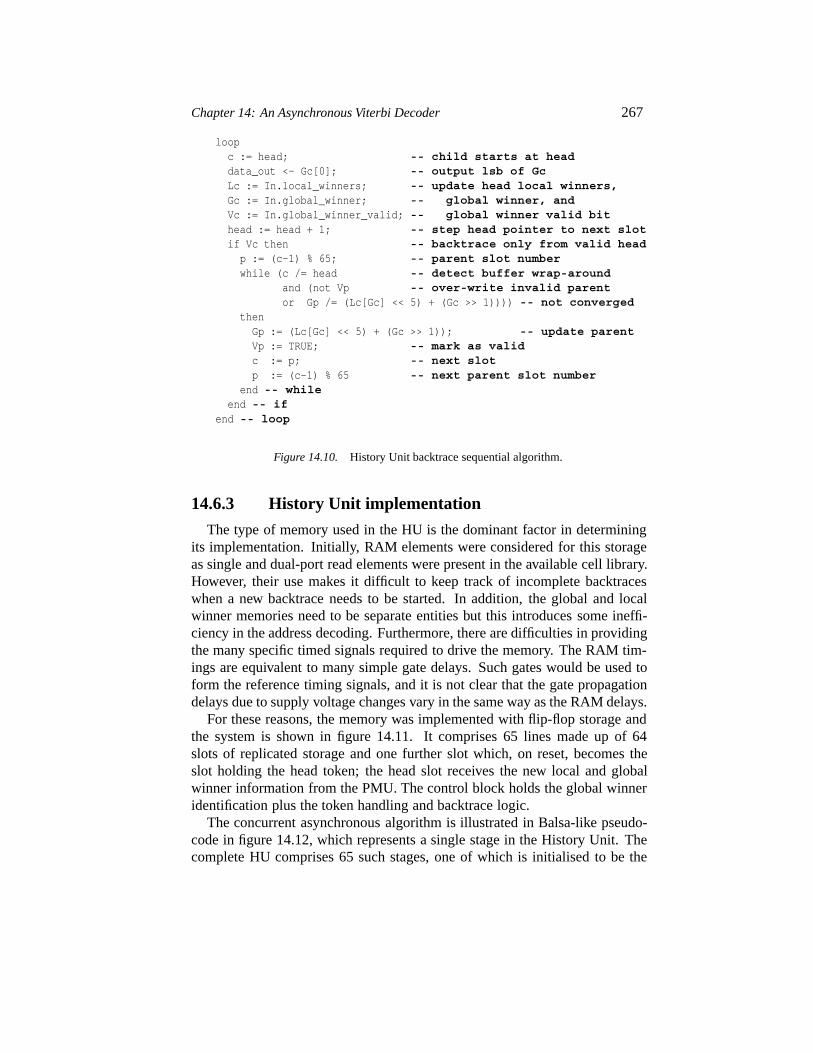
Chapter 14: An Asynchronous Viterbi Decoder 267
loopc := head; -- child starts at headdata_out <- Gc[0]; -- output lsb of GcLc := In.local_winners; -- update head local winners,Gc := In.global_winner; -- global winner, andVc := In.global_winner_valid; -- global winner valid bithead := head + 1; -- step head pointer to next slotif Vc then -- backtrace only from valid head
p := (c-1) % 65; -- parent slot numberwhile (c /= head -- detect buffer wrap-around
and (not Vp -- over-write invalid parentor Gp /= (Lc[Gc] << 5) + (Gc >> 1)))) -- not converged
thenGp := (Lc[Gc] << 5) + (Gc >> 1)); -- update parentVp := TRUE; -- mark as validc := p; -- next slotp := (c-1) % 65 -- next parent slot number
end -- whileend -- if
end -- loop
Figure 14.10. History Unit backtrace sequential algorithm.
14.6.3 History Unit implementation
The type of memory used in the HU is the dominant factor in determiningits implementation. Initially, RAM elements were considered for this storageas single and dual-port read elements were present in the available cell library.However, their use makes it difficult to keep track of incomplete backtraceswhen a new backtrace needs to be started. In addition, the global and localwinner memories need to be separate entities but this introduces some ineffi-ciency in the address decoding. Furthermore, there are difficulties in providingthe many specific timed signals required to drive the memory. The RAM tim-ings are equivalent to many simple gate delays. Such gates would be used toform the reference timing signals, and it is not clear that the gate propagationdelays due to supply voltage changes vary in the same way as the RAM delays.
For these reasons, the memory was implemented with flip-flop storage andthe system is shown in figure 14.11. It comprises 65 lines made up of 64slots of replicated storage and one further slot which, on reset, becomes theslot holding the head token; the head slot receives the new local and globalwinner information from the PMU. The control block holds the global winneridentification plus the token handling and backtrace logic.
The concurrent asynchronous algorithm is illustrated in Balsa-like pseudo-code in figure 14.12, which represents a single stage in the History Unit. Thecomplete HU comprises 65 such stages, one of which is initialised to be the
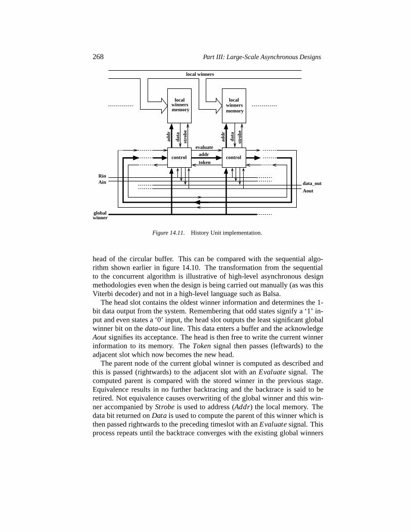
268 Part III: Large-Scale Asynchronous Designs
control
evaluate
addr
token
RinAin data_out
Aout
control
local winners
winners winnerslocal
memory
local
memory
addr
data
stro
be
addr
data
stro
be
winnerglobal
Figure 14.11. History Unit implementation.
head of the circular buffer. This can be compared with the sequential algo-rithm shown earlier in figure 14.10. The transformation from the sequentialto the concurrent algorithm is illustrative of high-level asynchronous designmethodologies even when the design is being carried out manually (as was thisViterbi decoder) and not in a high-level language such as Balsa.
The head slot contains the oldest winner information and determines the 1-bit data output from the system. Remembering that odd states signify a ‘1’ in-put and even states a ‘0’ input, the head slot outputs the least significant globalwinner bit on thedata-out line. This data enters a buffer and the acknowledgeAout signifies its acceptance. The head is then free to write the current winnerinformation to its memory. TheToken signal then passes (leftwards) to theadjacent slot which now becomes the new head.
The parent node of the current global winner is computed as described andthis is passed (rightwards) to the adjacent slot with anEvaluate signal. Thecomputed parent is compared with the stored winner in the previous stage.Equivalence results in no further backtracing and the backtrace is said to beretired. Not equivalence causes overwriting of the global winner and this win-ner accompanied byStrobe is used to address (Addr) the local memory. Thedata bit returned onData is used to compute the parent of this winner which isthen passed rightwards to the preceding timeslot with anEvaluate signal. Thisprocess repeats until the backtrace converges with the existing global winners
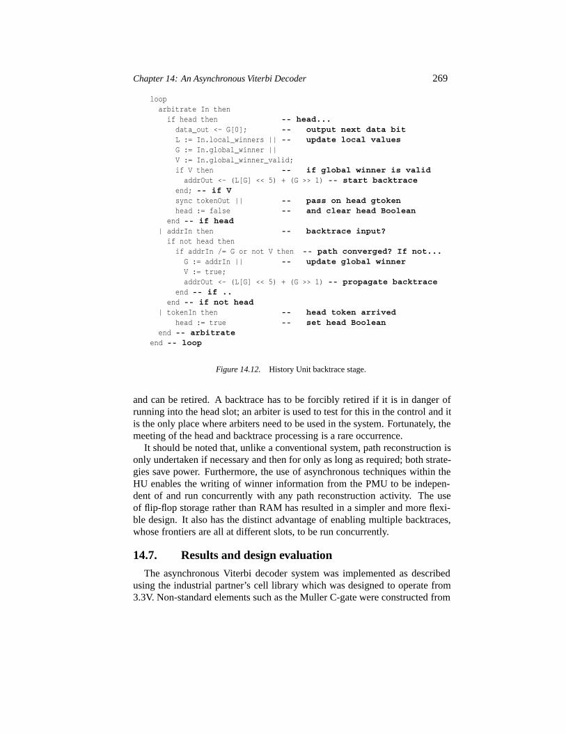
Chapter 14: An Asynchronous Viterbi Decoder 269
looparbitrate In then
if head then -- head...data_out <- G[0]; -- output next data bitL := In.local_winners || -- update local valuesG := In.global_winner ||V := In.global_winner_valid;if V then -- if global winner is validaddrOut <- (L[G] << 5) + (G >> 1) -- start backtrace
end; -- if Vsync tokenOut || -- pass on head gtokenhead := false -- and clear head Boolean
end -- if head| addrIn then -- backtrace input?
if not head thenif addrIn /= G or not V then -- path converged? If not...G := addrIn || -- update global winnerV := true;addrOut <- (L[G] << 5) + (G >> 1) -- propagate backtrace
end -- if ..end -- if not head
| tokenIn then -- head token arrivedhead := true -- set head Boolean
end -- arbitrateend -- loop
Figure 14.12. History Unit backtrace stage.
and can be retired. A backtrace has to be forcibly retired if it is in danger ofrunning into the head slot; an arbiter is used to test for this in the control and itis the only place where arbiters need to be used in the system. Fortunately, themeeting of the head and backtrace processing is a rare occurrence.
It should be noted that, unlike a conventional system, path reconstruction isonly undertaken if necessary and then for only as long as required; both strate-gies save power. Furthermore, the use of asynchronous techniques within theHU enables the writing of winner information from the PMU to be indepen-dent of and run concurrently with any path reconstruction activity. The useof flip-flop storage rather than RAM has resulted in a simpler and more flexi-ble design. It also has the distinct advantage of enabling multiple backtraces,whose frontiers are all at different slots, to be run concurrently.
14.7. Results and design evaluation
The asynchronous Viterbi decoder system was implemented as describedusing the industrial partner’s cell library which was designed to operate from3.3V. Non-standard elements such as the Muller C-gate were constructed from
270 Part III: Large-Scale Asynchronous Designs
the cell library; the only full-custom element which had to be designed was anarbiter.
Following simulation, the decoder was fabricated on a 0.35 micron CMOSprocess. Results for a 1/2 code rate, random input bit stream with no errorsshow an overall power dissipation of 1333 mW at 45 Msymbols/sec. Of this,the dissipation in the PMU dominates at 1233 mW while the HU takes only37 mW. The difference (about 60 mW) between these figure and those for theoverall consumption are accounted for by the dissipation in the BMU and inthe small amount of ‘glue’ logic prior to the BMU.
Errors in the input data to the decoder result in only small variations in thedissipation with the overall dissipation falling slightly with an increasing inputerror rate; internally, this decrease comprises a small reduction in the PMUdissipation and a smaller rise in the HU dissipation. The results for other coderates are a scaled version of those obtained for the 1/2 code rate as might beexpected. For example, a 3/4 code rate which receives 3 symbols for every 4clocks exhibits 1.5 times the dissipation of the 1/2 rate code with its 2 symbolsevery 4 clocks.
The asynchronous PMU performs approximately the same amount of workregardless of the number of errors in the data stream. This results from cappingnumbers at 6. This means that for a good data stream, all nodes have a weightof six except the one node on the good (correct) path. Thus the PMU is almostpermanently ‘saturated’ and practically all work performed relates to pathswhich will never be selected! Errors cause some spread in the node weightswith the higher weights (4, 5 and 6) predominating and the slightly smallercounts on some nodes accounts for the slight drop in dissipation in the PMUunder error conditions.
The asynchronous PMU dissipation is very high and does not compare wellwith synchronous PMUs using conventional parallel arithmetic to perform theadd, compare and select operation [15]. In order to understand why this occurs,it is necessary to examine the operation and logic used in the asynchronousPMU in more detail. With good (i.e. no error) data, 63 nodes have weightsof 6 and one node has a weight of 0. This translates to PMU activity on eachtimeslot where all State Metric FIFOs but one contain counts of 6 which arethen transferred to Path Metric FIFOs, whose counts of 6 are in turn removedfrom the Path Metric FIFOs, paired and transferred to the receiving State Met-ric FIFOs. Entering or removing a count of 6 from a FIFO involves 21 changesof state in the stages. Furthermore, the number of transitions actually involvedis higher due to (around 5) internal transitions on the elements making up theC-gates forming each FIFO stage. Thus, each of 63 nodes experiences around650 transitions just on the data path per timeslot. The control and other over-heads on the data path can be expected to form (say) an additional 30% oflogic. This indicates a node activity of around 850 transitions/timeslot and
Chapter 14: An Asynchronous Viterbi Decoder 271
overall the PMU can be expected to make a maximum of 54,400 transitions oneach timeslot.
Unfortunately, the design of the FIFOs, particularly the Path Metric FIFOs,has led to high capacitive loading on the true and inverse C-gate outputs ateach stage. A dissipation of 1233 mW with 54,400 transitions per slot and anenergy cost of 5�45�C joules per transition, whereC is the average track plusgate loading capacitance (in Farads), indicates an average loading of 92 fF andthis is confirmed by measurements.
By contrast, the HU power efficiency is excellent and is the real successstory in this design. Its dissipation is low and is far smaller than that in anyother system the designers are aware of. The HU dissipation demonstrates thatby keeping a good path, very little computing is required to output the datastream when there are no errors. Furthermore, when lots of noise is present,so that the backtrace process is active with many good paths in the process ofbeing reconstructed concurrently, the dissipation in the HU only rises slightly;this indicates that accessing the local winner memory in flip-flops and over-writing the global winner information is not a power-costly operation.
The HU dissipation also compares favourably with a (synchronous) systembuilt along similar principles to the HU described here but using RAM ele-ments from the library instead of flip-flops. Due to the limitations of the RAMdevices previously mentioned, these introduce additional complexity becauseonly one backtrace is performed at any time; it is therefore necessary to keeptrack of the depth reached by incomplete backtraces which are abandoned for anew backtrace leaving a partially complete global winner path reconstruction.The difference in dissipation between the asynchronous HU using flip-flopsand the other using RAMs reflects the power cost of accessing the local win-ner RAM and the associated significant additional computation involved in thebacktrace. This points to the power efficiency of storing the HU informationin a manner best suited to the task.
14.8. Conclusions
As in many asynchronous designs, the system design has had to be ap-proached from first principles and has caused a complete rethink about howto implement the Viterbi algorithm. This has resulted in a number of novelfeatures being incorporated in the PMU and HU units. In the PMU, the deci-sion to use serial unary arithmetic has enabled the conventional parallel add,compare and select logic to be dispensed with and replaced by dataless FIFOswhich perform the arithmetic serially.
While the PMU is an interesting and different design from that convention-ally used, its power consumption is not good. Its design illustrates that powerefficiency at the algorithmic and architecture levels needs to be combined with
272 Part III: Large-Scale Asynchronous Designs
efficient design at the logic, circuit and layout levels to realise the true po-tential of a system. This is demonstrated by a synchronous PMU constructedalong similar architectural principles to those described but implemented usinga low-power logic family and full custom layout which dissipates only 70 mWat 45 Msymbols/sec [15]. It is clear that while a full custom design of the asyn-chronous PMU datapath would reduce the current power levels significantly, amajor revision of the PMU logic for the datapath, paying particular attention toloading, is required for a design which has better power efficiency than othersystems.
The identification of a global winner is probably the most important advancein the PMU design. This has meant that both a good path and a local winnerhistory can be kept by the HU, leading to a greatly reduced amount of overallstorage required to deduce the output data. The use of flip-flop storage has alsogreatly contributed to the power efficiency of this unit and it does demonstratethe power advantages of optimising design at all levels in the design hierarchydown to and including the logic.
The HU also illustrates the advantages of asynchronous design in that theplacing of current information is decoupled from any backtracing operations ofwhich there may be many running concurrently. Furthermore, the speed of thebacktracing is only dependent on the logic required to perform this operationand not on any other internal or external system timing. Such a decoupled,multiple backtracing activity would clearly be more difficult to organise in thecontext of a synchronous timing environment.
14.8.1 Acknowledgement
As in any large project, a number of people have been engaged in the designand implementation of the Viterbi decoder described in this chapter. It is there-fore a pleasure to acknowledge the other colleagues in the Amulet group in theComputer Science Department at Manchester University involved at all stagesin this project, namely Mike Cumpstey, Steve Furber and Peter Riocreux. I amalso grateful to them for comments on the draft of this chapter.
14.8.2 Further reading
Further information on the Viterbi algorithm may be found in [148], [71]and [70]. Futher information on the PREST project is in [1].
Chapter 15
PROCESSORS�
Jim D. GarsideDepartment of Computer Science, The University of Manchester
Abstract Computer design becomes ever more complex. Small asynchronous systemsmay be intriguing and even elegant but unless asynchronous logic can not only becompetitive with ‘conventional’ logic but can show some significant advantagesit cannot be taken seriously in the commercial world.
There can be no better way to demonstrate the feasibility of something thanby doing it. To this end several research groups around have the world have beenputting together real, large, asynchronous systems. These have taken severalforms, but many groups have chosen to start with microprocessors; a processoris a good demonstrator because it is well defined, self-contained and forces a de-signer to solve problems which are already well understood. If an asynchronousimplementation of a microprocessor can comparefavourably with a synchronousdevice performing an identical function then the case is proven.
This chapter describes a number of processors that have been fabricated anddiscusses in some detail some of the solutions employed. The primary source ofthe material is the Amulet series of ARM implementations – because these arethe most familiar to the author – but other devices are included as appropriate.The later parts of the chapter widen the descriptions to include memory systems,cacheing and on-chip interconnect, illustrating how a complete asynchronousSystem on Chip (SoC) can be produced.
Keywords: low-power asynchronous circuits, processor architecture
�The majority of the work described in this chapter has been made possible by grants from the EuropeanUnion Open Microprocessor systems Initiative (OMI). The primary sources of funding have been OMI-MAP (Amulet1), OMI/DE-ARM (Amulet2e) and OMI/ATOM (Amulet3). Without this funding none ofthese devices would have been made and this support is gratefully acknowledged.
273
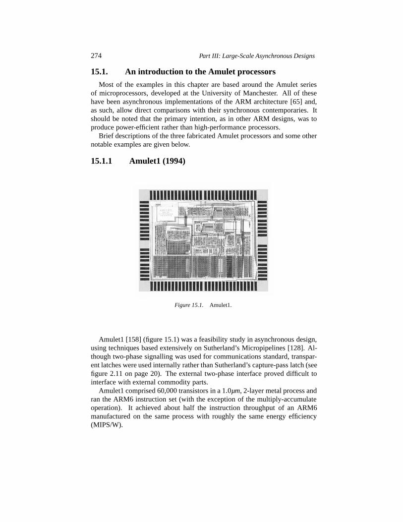
274 Part III: Large-Scale Asynchronous Designs
15.1. An introduction to the Amulet processors
Most of the examples in this chapter are based around the Amulet seriesof microprocessors, developed at the University of Manchester. All of thesehave been asynchronous implementations of the ARM architecture [65] and,as such, allow direct comparisons with their synchronous contemporaries. Itshould be noted that the primary intention, as in other ARM designs, was toproduce power-efficient rather than high-performance processors.
Brief descriptions of the three fabricated Amulet processors and some othernotable examples are given below.
15.1.1 Amulet1 (1994)
Figure 15.1. Amulet1.
Amulet1 [158] (figure 15.1) was a feasibility study in asynchronous design,using techniques based extensively on Sutherland’s Micropipelines [128]. Al-though two-phase signalling was used for communications standard, transpar-ent latches were used internally rather than Sutherland’s capture-pass latch (seefigure 2.11 on page 20). The external two-phase interface proved difficult tointerface with external commodity parts.
Amulet1 comprised 60,000 transistors in a 1�0µm, 2-layer metal process andran the ARM6 instruction set (with the exception of the multiply-accumulateoperation). It achieved about half the instruction throughput of an ARM6manufactured on the same process with roughly the same energy efficiency(MIPS/W).
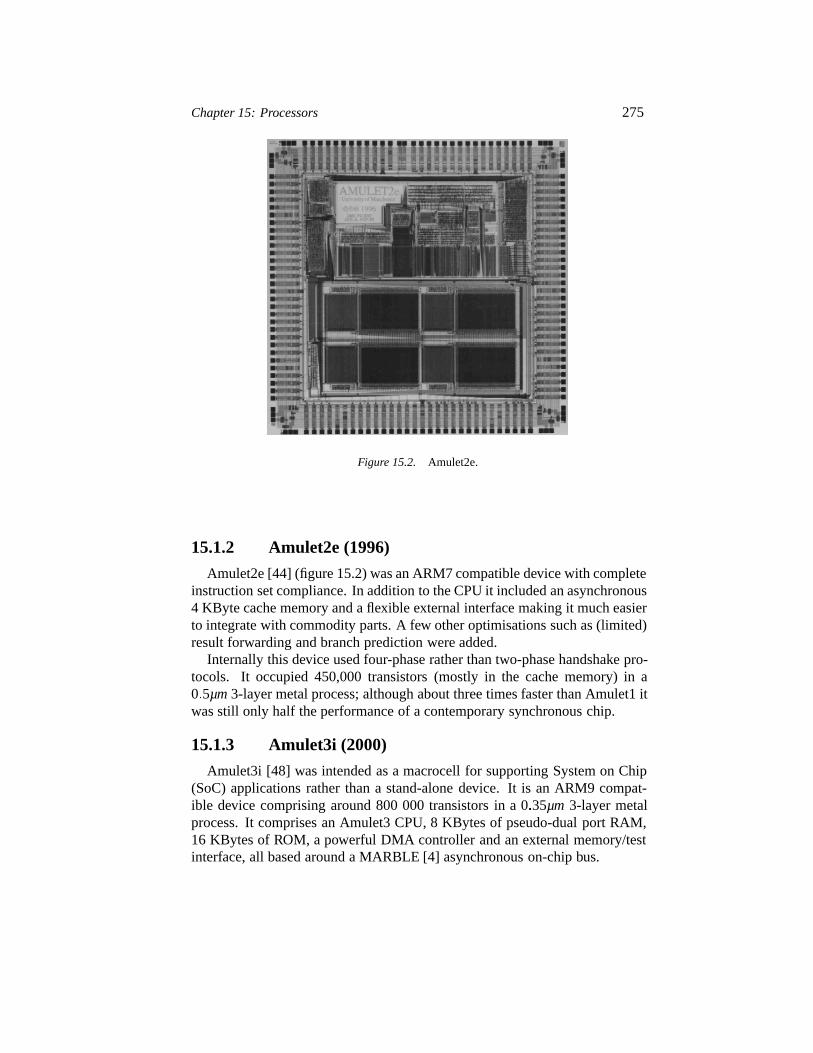
Chapter 15: Processors 275
Figure 15.2. Amulet2e.
15.1.2 Amulet2e (1996)
Amulet2e [44] (figure 15.2) was an ARM7 compatible device with completeinstruction set compliance. In addition to the CPU it included an asynchronous4 KByte cache memory and a flexible external interface making it much easierto integrate with commodity parts. A few other optimisations such as (limited)result forwarding and branch prediction were added.
Internally this device used four-phase rather than two-phase handshake pro-tocols. It occupied 450,000 transistors (mostly in the cache memory) in a0�5µm 3-layer metal process; although about three times faster than Amulet1 itwas still only half the performance of a contemporary synchronous chip.
15.1.3 Amulet3i (2000)
Amulet3i [48] was intended as a macrocell for supporting System on Chip(SoC) applications rather than a stand-alone device. It is an ARM9 compat-ible device comprising around 800 000 transistors in a 0�35µm 3-layer metalprocess. It comprises an Amulet3 CPU, 8 KBytes of pseudo-dual port RAM,16 KBytes of ROM, a powerful DMA controller and an external memory/testinterface, all based around a MARBLE [4] asynchronous on-chip bus.
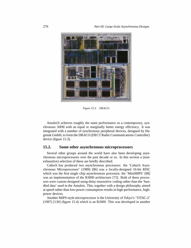
276 Part III: Large-Scale Asynchronous Designs
Figure 15.3. DRACO.
Amulet3i achieves roughly the same performance as a contemporary, syn-chronous ARM with an equal or marginally better energy efficiency. It wasintegrated with a number of synchronous peripheral devices, designed by Ha-genuk GmbH, to form the DRACO (DECT Radio Communications Controller)device (figure 15.3).
15.2. Some other asynchronous microprocessors
Several other groups around the world have also been developing asyn-chronous microprocessors over the past decade or so. In this section a (non-exhaustive) selection of these are briefly described.
Caltech has produced two asynchronous processors: the ‘Caltech Asyn-chronous Microprocessor’ (1989) [86] was a locally-designed 16-bit RISCwhich was the first single chip asynchronous processor; the ‘MiniMIPS’ [88]was an implementation of the R3000 architecture [72]. Both of these proces-sors were custom designed using delay-insensitive coding rather than the ‘bun-dled data’ used in the Amulets. This, together with a design philosophy aimedat speed rather than low-power consumption results in high-performance, high-power devices.
Another MIPS-style microprocessor is the University of Tokyo’s ‘TITAC-2’(1997) [130] (figure 15.4) which is an R2000. This was developed in another
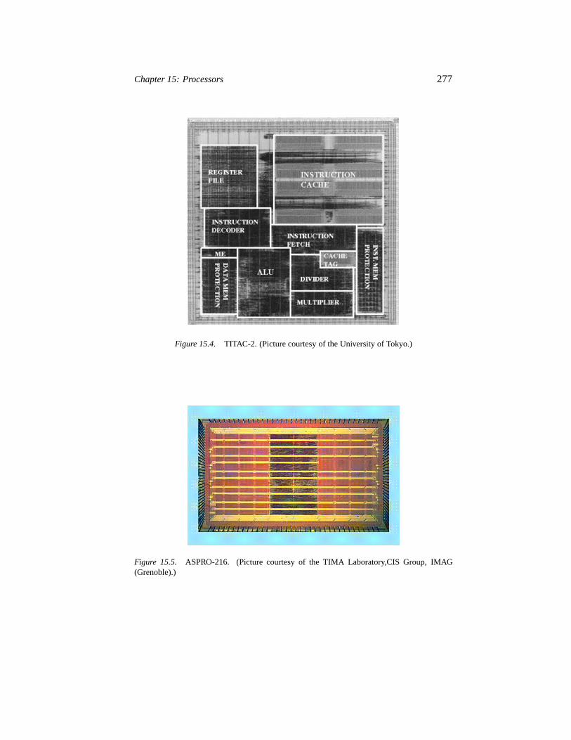
Chapter 15: Processors 277
Figure 15.4. TITAC-2. (Picture courtesy of the University of Tokyo.)
Figure 15.5. ASPRO-216. (Picture courtesy of the TIMA Laboratory,CIS Group, IMAG(Grenoble).)
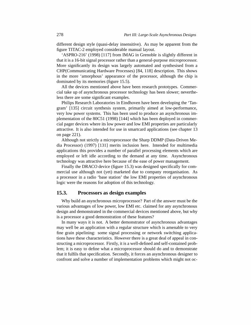
278 Part III: Large-Scale Asynchronous Designs
different design style (quasi-delay insensitive). As may be apparent from thefigure TITAC-2 employed considerable manual layout.
‘ASPRO-216’ (1998) [117] from IMAG in Grenoble is slightly different inthat it is a 16-bit signal processor rather than a general-purpose microprocessor.More significantly its design was largely automated and synthesised from aCHP(Communicating Hardware Processes) [84, 118] description. This showsin the more ‘amorphous’ appearance of the processor, although the chip isdominated by its memories (figure 15.5).
All the devices mentioned above have been research prototypes. Commer-cial take up of asynchronous processor technology has been slower; neverthe-less there are some significant examples.
Philips Research Laboratories in Eindhoven have been developing the ‘Tan-gram’ [135] circuit synthesis system, primarily aimed at low-performance,very low power systems. This has been used to produce an asynchronous im-plementation of the 80C51 (1998) [144] which has been deployed in commer-cial pager devices where its low power and low EMI properties are particularlyattractive. It is also intended for use in smartcard applications (see chapter 13on page 221).
Although not strictly a microprocessor the Sharp DDMP (Data-Driven Me-dia Processor) (1997) [131] merits inclusion here. Intended for multimediaapplications this provides a number of parallel processing elements which areemployed or left idle according to the demand at any time. Asynchronoustechnology was attractive here because of the ease of power management.
Finally the DRACO device (figure 15.3) was designed specifically for com-mercial use although not (yet) marketed due to company reorganisation. Asa processor in a radio ‘base station’ the low EMI properties of asynchronouslogic were the reasons for adoption of this technology.
15.3. Processors as design examples
Why build an asynchronous microprocessor? Part of the answer must be thevarious advantages of low power, low EMI etc. claimed for any asynchronousdesign and demonstrated in the commercial devices mentioned above, but whyis a processor a good demonstration of these features?
In many ways it is not. A better demonstrator of asynchronous advantagesmay well be an application with a regular structure which is amenable to veryfine grain pipelining: some signal processing or network switching applica-tions have these characteristics. However there is a great deal of appeal in con-structing a microprocessor. Firstly, it is a well-defined and self-contained prob-lem; it is easy to define what a microprocessor should do and to demonstratethat it fulfils that specification. Secondly, it forces an asynchronous designer toconfront and solve a number of implementation problems which might not oc-
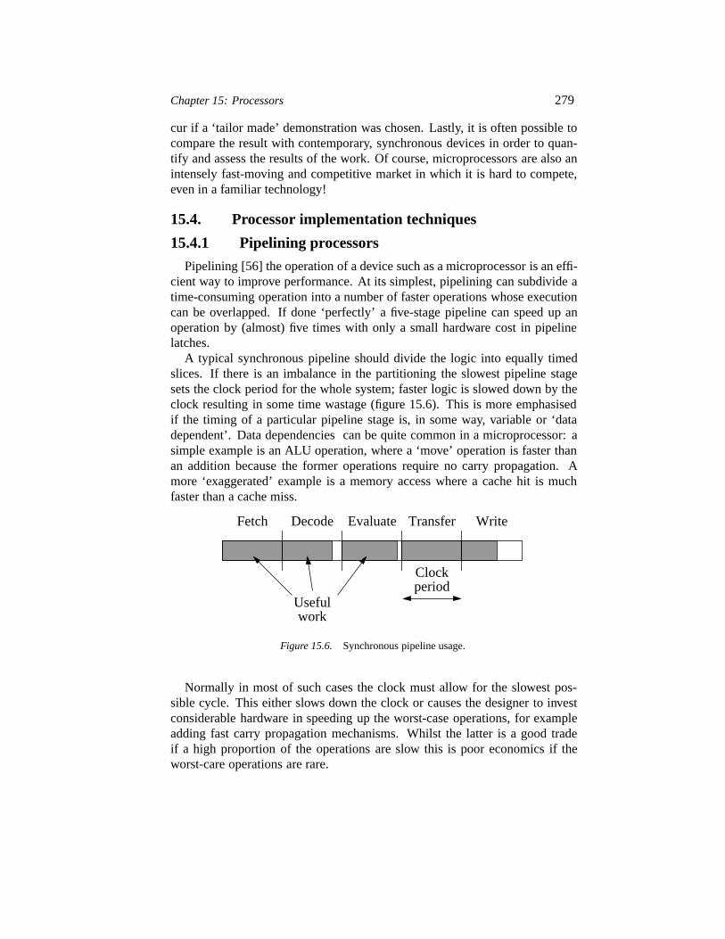
Chapter 15: Processors 279
cur if a ‘tailor made’ demonstration was chosen. Lastly, it is often possible tocompare the result with contemporary, synchronous devices in order to quan-tify and assess the results of the work. Of course, microprocessors are also anintensely fast-moving and competitive market in which it is hard to compete,even in a familiar technology!
15.4. Processor implementation techniques
15.4.1 Pipelining processors
Pipelining [56] the operation of a device such as a microprocessor is an effi-cient way to improve performance. At its simplest, pipelining can subdivide atime-consuming operation into a number of faster operations whose executioncan be overlapped. If done ‘perfectly’ a five-stage pipeline can speed up anoperation by (almost) five times with only a small hardware cost in pipelinelatches.
A typical synchronous pipeline should divide the logic into equally timedslices. If there is an imbalance in the partitioning the slowest pipeline stagesets the clock period for the whole system; faster logic is slowed down by theclock resulting in some time wastage (figure 15.6). This is more emphasisedif the timing of a particular pipeline stage is, in some way, variable or ‘datadependent’. Data dependencies can be quite common in a microprocessor: asimple example is an ALU operation, where a ‘move’ operation is faster thanan addition because the former operations require no carry propagation. Amore ‘exaggerated’ example is a memory access where a cache hit is muchfaster than a cache miss.
workUseful
periodClock
Fetch Decode Evaluate Transfer Write
Figure 15.6. Synchronous pipeline usage.
Normally in most of such cases the clock must allow for the slowest pos-sible cycle. This either slows down the clock or causes the designer to investconsiderable hardware in speeding up the worst-case operations, for exampleadding fast carry propagation mechanisms. Whilst the latter is a good tradeif a high proportion of the operations are slow this is poor economics if theworst-care operations are rare.
280 Part III: Large-Scale Asynchronous Designs
Another possible solution open to the synchronous designer is to allow cer-tain slow operations to occupy more than one clock cycle; this is clearly expe-dient when a cache miss occurs and the processor must idle until an off-chipmemory can be read. However multi-cycle operations introduce the need forsystem-wide clock control to stall other parts of the system; even then the tim-ing resolution is still limited to whole clock cycles.
Asynchronous pipelining is conceptually much easier. Not only is all con-trol localised, but it is implicitly adaptable to pipeline stages with variable de-lays. This means that rare, worst-case operations can be accommodated with-out either excessive hardware investment or a significant impact in the overallprocessing time by altering the delay of a pipeline stage dynamically. This,combined with the fact that operations can flow at their own rate rather thanbeing stacked one to a stage, gives the pipeline considerable ‘elasticity’. Insuch a pipeline a cache miss still occupies a single cycle, although that cyclewill be a particularly slow one!
Another clear example of this is visible in the ARM instruction set [65]where data processing operations and address calculations may specify anoperand shift before the ALU operation. In early ARM implementations thiswas contained in a single pipeline stage and hidden by the slower memory ac-cess time. To avoid a performance penalty more modern synchronous designshave the options of:
an additional shifter pipeline stage (increases latency);
stalling for an extra clock when a shift is required (increases complex-ity).
An asynchronous pipeline can simply stretch the execution cycle when re-quired. As the additional time is unlikely to be as long as the ALU stage delaythis is more flexible than either of the synchronous options, and the overallimpact is small because shift/operate operations are quite rare.
‘Average case’ performance. The elasticity of an asynchronous pipeline hasled to the myth that an asynchronous pipeline can perform its processing in an‘average’ rather than worst case time for each pipeline stage. This is true onlyif the unit under consideration is kept constantly busy. This will not be true inthe general case: on some occasions the unit will be ready before its operandsand at other times it will have completed before subsequent stages can acceptits output; in each case an interlude of idleness is enforced. This effect can bereduced by providing fast buffers between processing elements to allow some‘play’ in the timing, but true average case behaviour can only be achieved withbuffers of infinite size. Any buffering increases the pipeline latency and shouldtherefore be used with circumspection.
Chapter 15: Processors 281
In practice an asynchronous pipeline should be balanced in a similar fashionto a synchronous pipeline. The difference is that occasional, time consumingoperations can be accommodated without either pipeline disruption or signif-icant extra hardware. An added bonus is that the pipeline latency, especiallywhen filling an ‘empty’ pipeline, can be reduced because the first instructionis not retarded by the clock at each stage (figure 15.6). The problem then de-volves into partitioning the system and solving the resulting problem of internaloperand dependences.
15.4.2 Asynchronous pipeline architectures
Once an asynchronous pipeline has been developed it is very easy to addpipeline stages to a design. However, pipelining indiscriminately can be a BadThing, at least in a general-purpose processor. The major reason for this isthe need to resolve dependencies [56], where one operation must gather itsoperands from the results of previous instructions; if many operations are inthe pipeline simultaneously it is quite likely that any new instructions will beforced to wait for some of these to complete. Resolving dependencies in anasynchronous environment can be a relatively complex task and is discussed ina later section.
A less obvious consequence is the increase in latency in the pipeline, notonly due to added latch delays but because, in some circumstances, the pipelineneeds to drain and refill. Consider a processor pipeline with a fast FIFO bufferacting as a prefetch buffer; this initially seems like a good idea as it can helpreduce stalls due to (for example) occasional slow cycles in the prefetch (e.g.cache miss) and execution (e.g. multiplication) stages. However, at least ina general purpose processor, this benefit is masked because a single stall canfill up the prefetch buffer and, typically shortly thereafter, a branch requires itto be drained. This was an architectural error evidenced in Amulet1, whichsuffered a noticeable performance penalty due to its four-stage prefetch buffer.Of course in other applications, where pipeline flushes are rare, the ease ofadding buffering can provide significant gains; however experience has shownthat for a general purpose CPU a more conventional approach producing areasonably balanced pipeline based around a known cycle time (such as thecache read-hit cycle time) is the ‘best’ approach.
One definite advantage of an asynchronous pipeline is that the pipeline flowcan be controlled locally. Consider that bane of the RISC architecture themulti-cycle instruction; in a synchronous environment such an operation mustbe able to suspend large parts or all of the processing pipeline, necessitating awidespread control network. In an asynchronous environment the system neednot be aware of operations in other parts of the system; instead a multi-cycle
282 Part III: Large-Scale Asynchronous Designs
operation simply appears as a longer delay, possibly causing a stall if otherprocessing elements require interaction with the busy unit(s).
In the ARM architecture there is one case where this ability is very useful;the multiple register load and store operations (LDM/STM) can transfer anarbitrary subset of the sixteen current registers to or from memory. Amulet3implements this by generating several local ‘instruction’ packets for the exe-cution stages for a single input handshake. At this point it is likely that theprefetch will fill up the intervening latches and stall, but this is a natural con-sequence of the pipeline’s operation.
There are other examples of this behaviour in Amulet3 (figure 15.7), notablythe Thumb decoder which ingests 32-bit packets which can contain either oneARM instruction or two of the ‘compressed’, 16-bit Thumb instructions. Inthe latter case two output handshakes are generated for each input. This pro-vides an advantage over earlier (synchronous) Thumb implementations, whichfetch instructions sixteen bits at a time, because it reduces the number of in-struction fetch memory cycles and, with a slow memory, uses the full availablebandwidth. The power consumption in the memory system is also reducedcommensurately.
Local control is also possible in instructions such as ‘CMP’ (compare) whichdo not need to traverse the entire pipeline length; it is just as easy to remove apacket from the pipeline by generating no output handshakes as it is to generateextra packets. In Amulet3 comparison operations only affect the processor’sflags which reside in the ‘execute’ stage and therefore cause no activity furtherdown the pipeline.
A final benefit of the localised control is that the pipeline operation canbe regulated by any active stage. Both Amulet2 and Amulet3 have retrofitted a‘halt’ (until interrupted) instruction into the ARM instruction set (implementedtransparently from an instruction which branches to itself). This can be de-tected and ‘executed’ anywhere within the pipeline with the same effect ofcausing the processor to stall. Indeed Amulet2 instigates halts in its executionunit whereas Amulet3 halts by suspending instruction prefetch, but the over-all effect is the same. Halting an asynchronous processor (or part thereof) isequivalent to stopping the clock in a synchronous processor and, in a CMOSprocess, can drop the power consumption to near zero. This facility thereforemakes power management particularly easy and – in many cases – near auto-matic.
15.4.3 Determinism and non-determinism
Before examining specific architectural techniques which can be employedin an asynchronous processor it is worth considering something of the de-sign philosophies employed. The most significant is probably that of non-
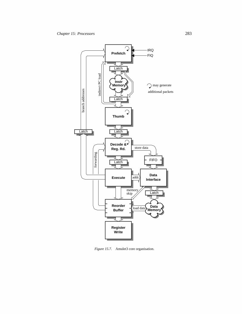
Chapter 15: Processors 283
Latch
Execute InterfaceData
FIFO
Buffer
Latch
Decode &
Latch
Register
Latch
Prefetch
Reorder
Write
Latch
Reg. Rd.
Thumb
skipmemory
FIQ
IRQ
Latch
InstrMemory may generate
additional packets
bran
ch a
ddre
sses
forw
ardi
ngin
dire
ct P
C lo
ad
store data
addr.
load dataMemoryData
Figure 15.7. Amulet3 core organisation.
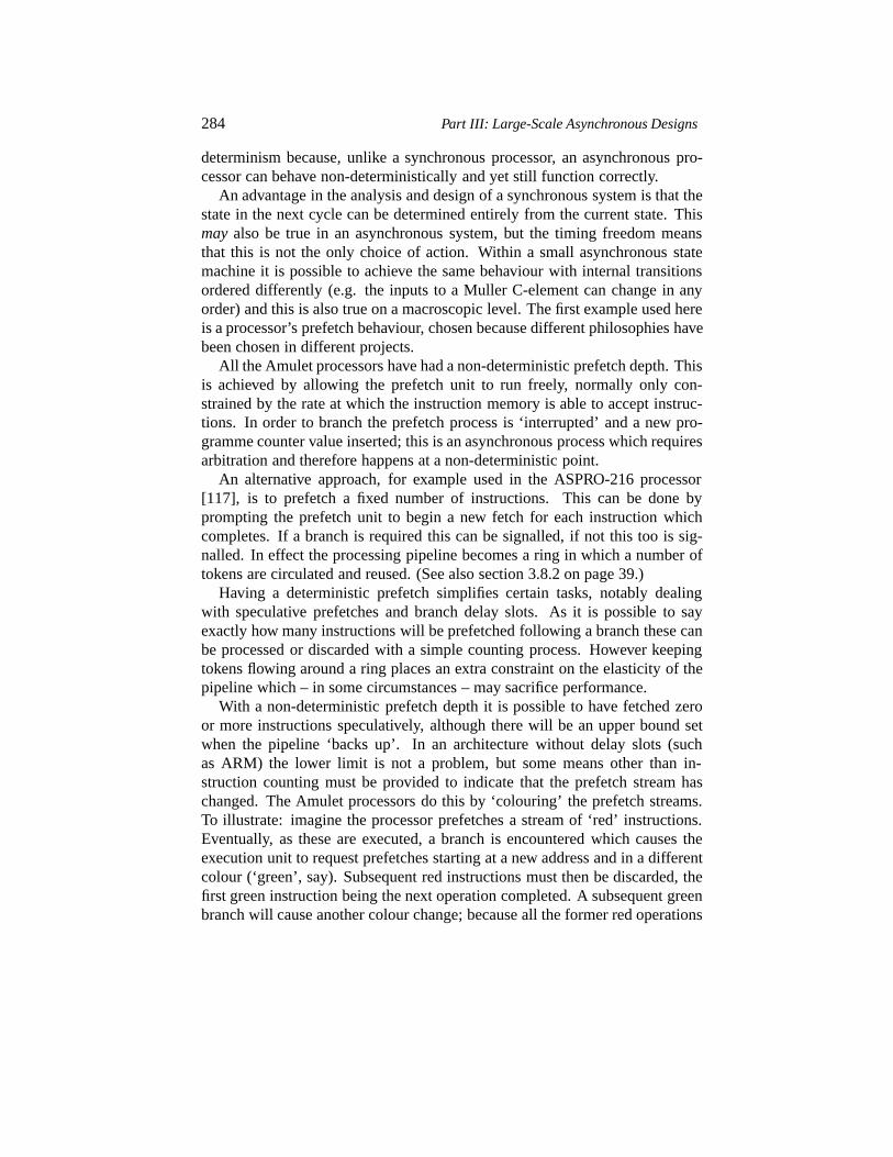
284 Part III: Large-Scale Asynchronous Designs
determinism because, unlike a synchronous processor, an asynchronous pro-cessor can behave non-deterministically and yet still function correctly.
An advantage in the analysis and design of a synchronous system is that thestate in the next cycle can be determined entirely from the current state. Thismay also be true in an asynchronous system, but the timing freedom meansthat this is not the only choice of action. Within a small asynchronous statemachine it is possible to achieve the same behaviour with internal transitionsordered differently (e.g. the inputs to a Muller C-element can change in anyorder) and this is also true on a macroscopic level. The first example used hereis a processor’s prefetch behaviour, chosen because different philosophies havebeen chosen in different projects.
All the Amulet processors have had a non-deterministic prefetch depth. Thisis achieved by allowing the prefetch unit to run freely, normally only con-strained by the rate at which the instruction memory is able to accept instruc-tions. In order to branch the prefetch process is ‘interrupted’ and a new pro-gramme counter value inserted; this is an asynchronous process which requiresarbitration and therefore happens at a non-deterministic point.
An alternative approach, for example used in the ASPRO-216 processor[117], is to prefetch a fixed number of instructions. This can be done byprompting the prefetch unit to begin a new fetch for each instruction whichcompletes. If a branch is required this can be signalled, if not this too is sig-nalled. In effect the processing pipeline becomes a ring in which a number oftokens are circulated and reused. (See also section 3.8.2 on page 39.)
Having a deterministic prefetch simplifies certain tasks, notably dealingwith speculative prefetches and branch delay slots. As it is possible to sayexactly how many instructions will be prefetched following a branch these canbe processed or discarded with a simple counting process. However keepingtokens flowing around a ring places an extra constraint on the elasticity of thepipeline which – in some circumstances – may sacrifice performance.
With a non-deterministic prefetch depth it is possible to have fetched zeroor more instructions speculatively, although there will be an upper bound setwhen the pipeline ‘backs up’. In an architecture without delay slots (suchas ARM) the lower limit is not a problem, but some means other than in-struction counting must be provided to indicate that the prefetch stream haschanged. The Amulet processors do this by ‘colouring’ the prefetch streams.To illustrate: imagine the processor prefetches a stream of ‘red’ instructions.Eventually, as these are executed, a branch is encountered which causes theexecution unit to request prefetches starting at a new address and in a differentcolour (‘green’, say). Subsequent red instructions must then be discarded, thefirst green instruction being the next operation completed. A subsequent greenbranch will cause another colour change; because all the former red operations
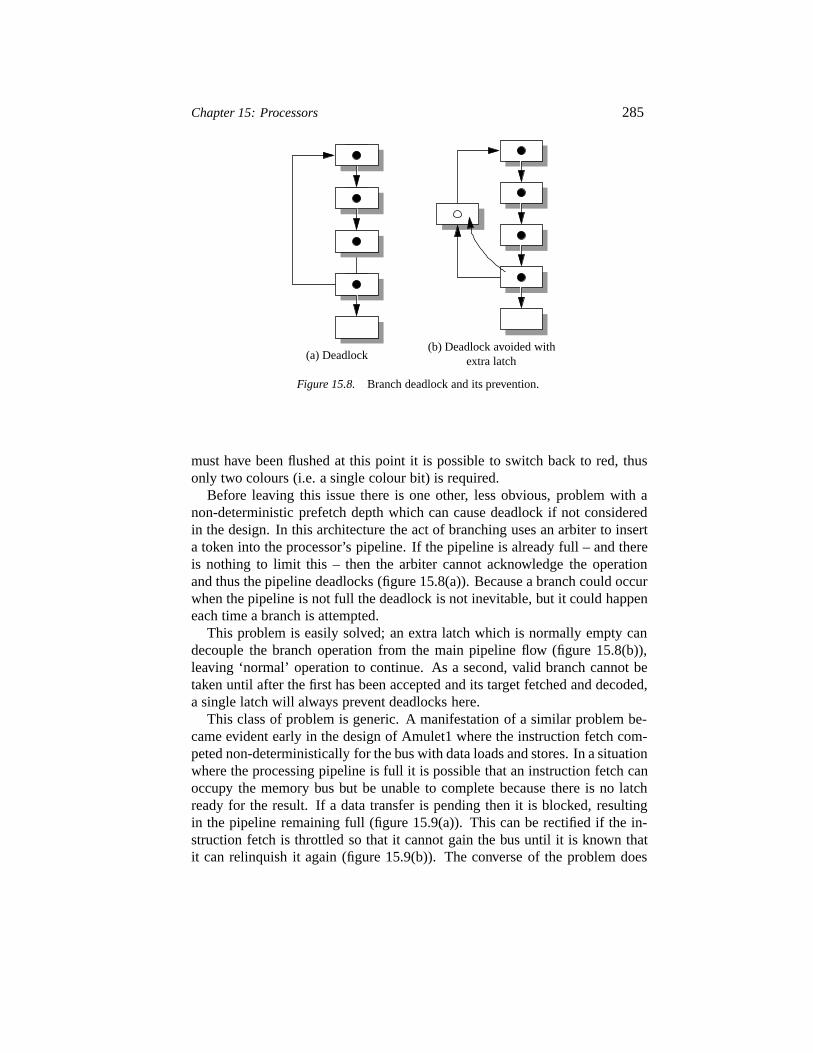
Chapter 15: Processors 285
(a) Deadlock(b) Deadlock avoided with
extra latch
Figure 15.8. Branch deadlock and its prevention.
must have been flushed at this point it is possible to switch back to red, thusonly two colours (i.e. a single colour bit) is required.
Before leaving this issue there is one other, less obvious, problem with anon-deterministic prefetch depth which can cause deadlock if not consideredin the design. In this architecture the act of branching uses an arbiter to inserta token into the processor’s pipeline. If the pipeline is already full – and thereis nothing to limit this – then the arbiter cannot acknowledge the operationand thus the pipeline deadlocks (figure 15.8(a)). Because a branch could occurwhen the pipeline is not full the deadlock is not inevitable, but it could happeneach time a branch is attempted.
This problem is easily solved; an extra latch which is normally empty candecouple the branch operation from the main pipeline flow (figure 15.8(b)),leaving ‘normal’ operation to continue. As a second, valid branch cannot betaken until after the first has been accepted and its target fetched and decoded,a single latch will always prevent deadlocks here.
This class of problem is generic. A manifestation of a similar problem be-came evident early in the design of Amulet1 where the instruction fetch com-peted non-deterministically for the bus with data loads and stores. In a situationwhere the processing pipeline is full it is possible that an instruction fetch canoccupy the memory bus but be unable to complete because there is no latchready for the result. If a data transfer is pending then it is blocked, resultingin the pipeline remaining full (figure 15.9(a)). This can be rectified if the in-struction fetch is throttled so that it cannot gain the bus until it is known thatit can relinquish it again (figure 15.9(b)). The converse of the problem does
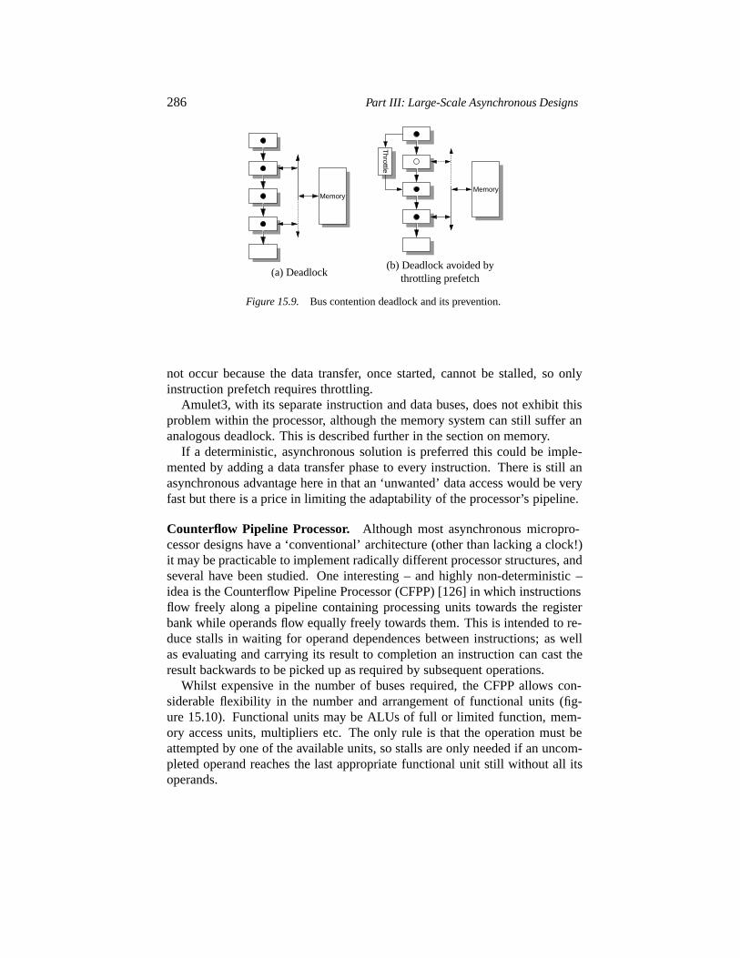
286 Part III: Large-Scale Asynchronous Designs
Memory
(a) Deadlock
Throttle
Memory
(b) Deadlock avoided bythrottling prefetch
Figure 15.9. Bus contention deadlock and its prevention.
not occur because the data transfer, once started, cannot be stalled, so onlyinstruction prefetch requires throttling.
Amulet3, with its separate instruction and data buses, does not exhibit thisproblem within the processor, although the memory system can still suffer ananalogous deadlock. This is described further in the section on memory.
If a deterministic, asynchronous solution is preferred this could be imple-mented by adding a data transfer phase to every instruction. There is still anasynchronous advantage here in that an ‘unwanted’ data access would be veryfast but there is a price in limiting the adaptability of the processor’s pipeline.
Counterflow Pipeline Processor. Although most asynchronous micropro-cessor designs have a ‘conventional’ architecture (other than lacking a clock!)it may be practicable to implement radically different processor structures, andseveral have been studied. One interesting – and highly non-deterministic –idea is the Counterflow Pipeline Processor (CFPP) [126] in which instructionsflow freely along a pipeline containing processing units towards the registerbank while operands flow equally freely towards them. This is intended to re-duce stalls in waiting for operand dependences between instructions; as wellas evaluating and carrying its result to completion an instruction can cast theresult backwards to be picked up as required by subsequent operations.
Whilst expensive in the number of buses required, the CFPP allows con-siderable flexibility in the number and arrangement of functional units (fig-ure 15.10). Functional units may be ALUs of full or limited function, mem-ory access units, multipliers etc. The only rule is that the operation must beattempted by one of the available units, so stalls are only needed if an uncom-pleted operand reaches the last appropriate functional unit still without all itsoperands.
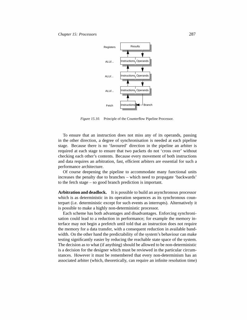
Chapter 15: Processors 287
InstructionsFetch
ALU/...
ALU/...
ALU/... Instructions Operands
Instructions Operands
Instructions Operands
Registers
Branch
Results
Figure 15.10. Principle of the Counterflow Pipeline Processor.
To ensure that an instruction does not miss any of its operands, passingin the other direction, a degree of synchronisation is needed at each pipelinestage. Because there is no ‘favoured’ direction in the pipeline an arbiter isrequired at each stage to ensure that two packets do not ‘cross over’ withoutchecking each other’s contents. Because every movement of both instructionsand data requires an arbitration, fast, efficient arbiters are essential for such aperformance architecture.
Of course deepening the pipeline to accommodate many functional unitsincreases the penalty due to branches – which need to propagate ‘backwards’to the fetch stage – so good branch prediction is important.
Arbitration and deadlock. It is possible to build an asynchronous processorwhich is as deterministic in its operation sequences as its synchronous coun-terpart (i.e. deterministic except for such events as interrupts). Alternatively itis possible to make a highly non-deterministic processor.
Each scheme has both advantages and disadvantages. Enforcing synchroni-sation could lead to a reduction in performance; for example the memory in-terface may not begin a prefetch until told that an instruction does not requirethe memory for a data transfer, with a consequent reduction in available band-width. On the other hand the predictability of the system’s behaviour can maketesting significantly easier by reducing the reachable state space of the system.The decision as to what (if anything) should be allowed to be non-deterministicis a decision for the designer which must be reviewed in the particular circum-stances. However it must be remembered that every non-determinism has anassociated arbiter (which, theoretically, can require an infinite resolution time)
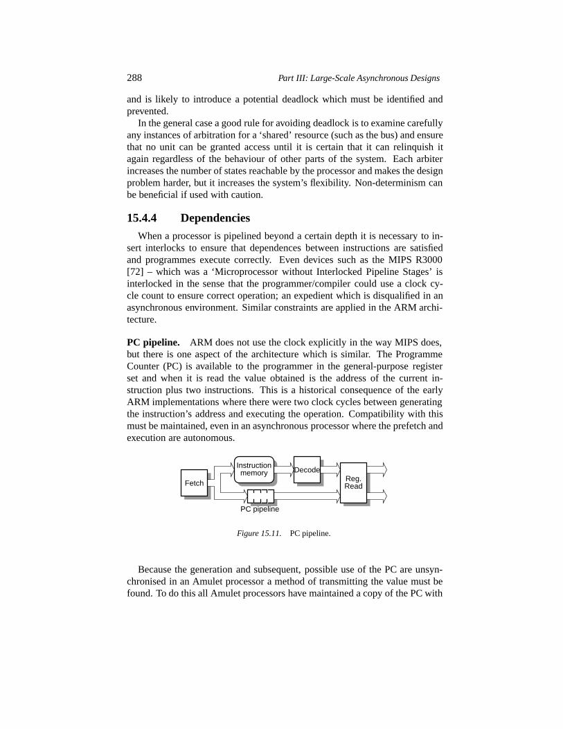
288 Part III: Large-Scale Asynchronous Designs
and is likely to introduce a potential deadlock which must be identified andprevented.
In the general case a good rule for avoiding deadlock is to examine carefullyany instances of arbitration for a ‘shared’ resource (such as the bus) and ensurethat no unit can be granted access until it is certain that it can relinquish itagain regardless of the behaviour of other parts of the system. Each arbiterincreases the number of states reachable by the processor and makes the designproblem harder, but it increases the system’s flexibility. Non-determinism canbe beneficial if used with caution.
15.4.4 Dependencies
When a processor is pipelined beyond a certain depth it is necessary to in-sert interlocks to ensure that dependences between instructions are satisfiedand programmes execute correctly. Even devices such as the MIPS R3000[72] – which was a ‘Microprocessor without Interlocked Pipeline Stages’ isinterlocked in the sense that the programmer/compiler could use a clock cy-cle count to ensure correct operation; an expedient which is disqualified in anasynchronous environment. Similar constraints are applied in the ARM archi-tecture.
PC pipeline. ARM does not use the clock explicitly in the way MIPS does,but there is one aspect of the architecture which is similar. The ProgrammeCounter (PC) is available to the programmer in the general-purpose registerset and when it is read the value obtained is the address of the current in-struction plus two instructions. This is a historical consequence of the earlyARM implementations where there were two clock cycles between generatingthe instruction’s address and executing the operation. Compatibility with thismust be maintained, even in an asynchronous processor where the prefetch andexecution are autonomous.
memoryInstruction
Read
DecodeReg.
PC pipeline
Fetch
Figure 15.11. PC pipeline.
Because the generation and subsequent, possible use of the PC are unsyn-chronised in an Amulet processor a method of transmitting the value must befound. To do this all Amulet processors have maintained a copy of the PC with
Chapter 15: Processors 289
each fetched instruction (figure 15.11). These flow down the pipeline with theinstruction and can be read whenever the PC may be needed. The PC may berequired explicitly as an operand or address, implicitly in branch instructions,or to find a return address in the case of exceptions such as interrupts or mem-ory aborts. Different Amulet cores have varied the exact value (e.g. PC+8)held with this ‘PC pipeline’ in attempts to minimise the later calculation over-heads, but in Amulet3 the PC is held without any premodification which allowsany of the required values PC+2, PC+4, PC+8 to be calculated with a simpleincrementer.
It is worth noting that the PC values need not be bundled with the instructiondirectly. The PC pipeline can be a separate, asynchronous pipeline from theinstruction fetch which can have a different depth, providing that a ‘one in,one out’ correspondence is maintained. This is a feature which is exploited inAmulet3 to throttle the prefetch unit and prevent instruction fetches causing adeadlock; this mechanism is described more fully in section 15.5.2.
Register dependencies. The greatest register dependency problems are read-after-write dependencies. One of these occurs in the case of a fragment of codesuch as:
LDR R1, [R0] ; Load ...ADD R2, R1, R3 ; ... and read
In this example it is essential that the value is (at least apparently) loadedinto R1 before the subsequent instruction uses it. As soon as the executionpath is pipelined there is a risk that this will not be assured and this uncertaintyis increased in an asynchronous device where the load could take an arbitrarytime.
Three solutions for ensuring register bank dependencies are satisfied aregiven below.
Don’t pipeline.
Lock.
Forward.
The first solution was the approach taken in the earliest, synchronous ARMimplementations. This involves reading register operands, performing an oper-ation and writing the result back in a single cycle so that a subsequent operationalways has a ‘clean’ register view. This is simple but makes the evaluation cy-cle very long and is unacceptable in a high-performance processor.
A locking approach allows selective pipelining of the instruction executionby retarding instructions whose operand registers are not yet valid. This in-volves setting a ‘lock’ flag when an instruction is decoded which wishes to
290 Part III: Large-Scale Asynchronous Designs
modify a register and clearing the flag again when the value finally arrives. Asubsequent instruction can test the locks on its operands and be delayed untilthey are all clear. This mechanism is eminently suited to an asynchronous im-plementation because a stalled instruction is simply caused to wait, which canbe done without recourse to arbitration.
In practice it is convenient to allow more than one result to be outstandingfor a single register. Partly this is a consequence of the ARM’s extensive useof conditional instructions, such as:
CMP R1, R2 ; Set flagsMOVNE R0, #-1 ; If R1 ? R2MOVEQ R0, #1 ; If R1 = R2
In such a case a single lock flag (on R0 in this instance) is inadequate andsome form of semaphore is needed. It turns out that the operation of sucha semaphore is fairly simple to implement in an asynchronous environmentprovided that testing and incrementing are mutually exclusive. At issue timean instruction therefore:
attempts to read its operands and waits until they are all unlocked, then
locks its register destination(s) by incrementing the semaphore.
The semaphore is decremented again when the result is returned; this actionmay take the semaphore to zero and, possibly, free up a waiting instruction.This can happen at any time.
The example above illustrates another potential problem in an asynchronoussystem: the two ‘MOV’ operations are mutually exclusive and so only one willbe executed. As this is not known at issue time both have incremented thesemaphore and so both must decrement it, otherwise R0 will be permanentlylocked. In general if a speculative operation is begun it must complete – the‘write’ operation therefore always takes place, although sometimes the registercontents are not changed and only the unlocking is performed.
The principle of semaphores was designed and implemented as the ‘lockFIFO’ in Amulet1 and Amulet2. In these processors the semaphore also heldthe destination register addresses to avoid carrying them with the instruction.As the instructions flowed (largely) in order, results and destinations could bepaired at write time.
The lock FIFO was implemented as an asynchronous pipeline as shown infigure 15.12. Because the cells in each latch (horizontal) are transparent latchesthe entries are copied from one to the next, thus ensuring the outputs of the ORgates are glitch free. These can then be used to stall any read operations onthe particular register until the write is complete. The only hazard would beif a register was actively locked whilst a read was being attempted; this isprevented by a sequencing of read-then-lock by the instruction decoder.
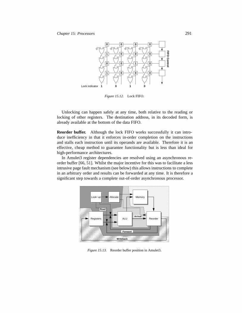
Chapter 15: Processors 291
Lock indicator 1 0 1 0
0
0
0
0
000
1
0
1 0
0
0 0
1
0
FIF
O C
on
trol
Figure 15.12. Lock FIFO.
Unlocking can happen safely at any time, both relative to the reading orlocking of other registers. The destination address, in its decoded form, isalready available at the bottom of the data FIFO.
Reorder buffer. Although the lock FIFO works successfully it can intro-duce inefficiency in that it enforces in-order completion on the instructionsand stalls each instruction until its operands are available. Therefore it is aneffective, cheap method to guarantee functionality but is less than ideal forhigh-performance architectures.
In Amulet3 register dependencies are resolved using an asynchronous re-order buffer [66, 51]. Whilst the major incentive for this was to facilitate a lessintrusive page fault mechanism (see below) this allows instructions to completein an arbitrary order and results can be forwarded at any time. It is therefore asignificant step towards a complete out-of-order asynchronous processor.
����������������������������������������������������������������������������������������������������������������������������������������������������������������������������������������������������������������������������������������������������������
����������������������������������������������������������������������������������������������������������������������������������������������������������������������������������������������������������������������������������������������������������
Look−up
ALURegisters Reorder
Memory
Read
Arrival
Forward
Writeback
Allocate
Figure 15.13. Reorder buffer position in Amulet3.
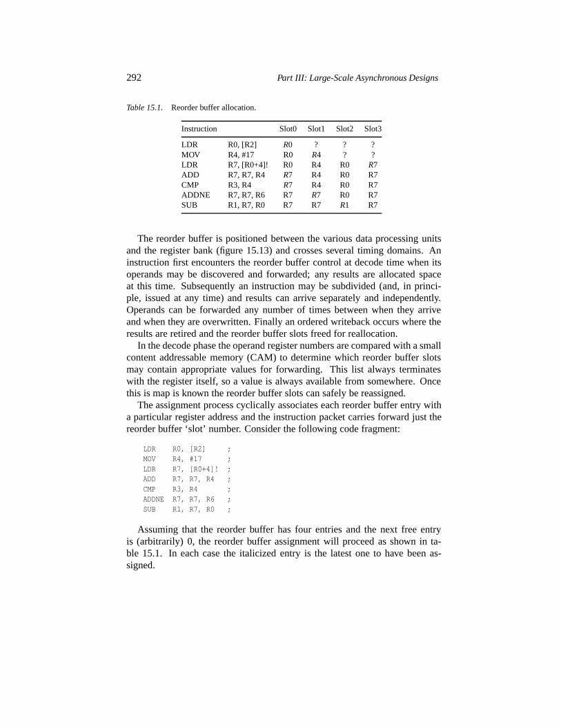
292 Part III: Large-Scale Asynchronous Designs
Table 15.1. Reorder buffer allocation.
Instruction Slot0 Slot1 Slot2 Slot3
LDR R0, [R2] R0 ? ? ?MOV R4, #17 R0 R4 ? ?LDR R7, [R0+4]! R0 R4 R0 R7ADD R7, R7, R4 R7 R4 R0 R7CMP R3, R4 R7 R4 R0 R7ADDNE R7, R7, R6 R7 R7 R0 R7SUB R1, R7, R0 R7 R7 R1 R7
The reorder buffer is positioned between the various data processing unitsand the register bank (figure 15.13) and crosses several timing domains. Aninstruction first encounters the reorder buffer control at decode time when itsoperands may be discovered and forwarded; any results are allocated spaceat this time. Subsequently an instruction may be subdivided (and, in princi-ple, issued at any time) and results can arrive separately and independently.Operands can be forwarded any number of times between when they arriveand when they are overwritten. Finally an ordered writeback occurs where theresults are retired and the reorder buffer slots freed for reallocation.
In the decode phase the operand register numbers are compared with a smallcontent addressable memory (CAM) to determine which reorder buffer slotsmay contain appropriate values for forwarding. This list always terminateswith the register itself, so a value is always available from somewhere. Oncethis is map is known the reorder buffer slots can safely be reassigned.
The assignment process cyclically associates each reorder buffer entry witha particular register address and the instruction packet carries forward just thereorder buffer ‘slot’ number. Consider the following code fragment:
LDR R0, [R2] ;MOV R4, #17 ;LDR R7, [R0+4]! ;ADD R7, R7, R4 ;CMP R3, R4 ;ADDNE R7, R7, R6 ;SUB R1, R7, R0 ;
Assuming that the reorder buffer has four entries and the next free entryis (arbitrarily) 0, the reorder buffer assignment will proceed as shown in ta-ble 15.1. In each case the italicized entry is the latest one to have been as-signed.
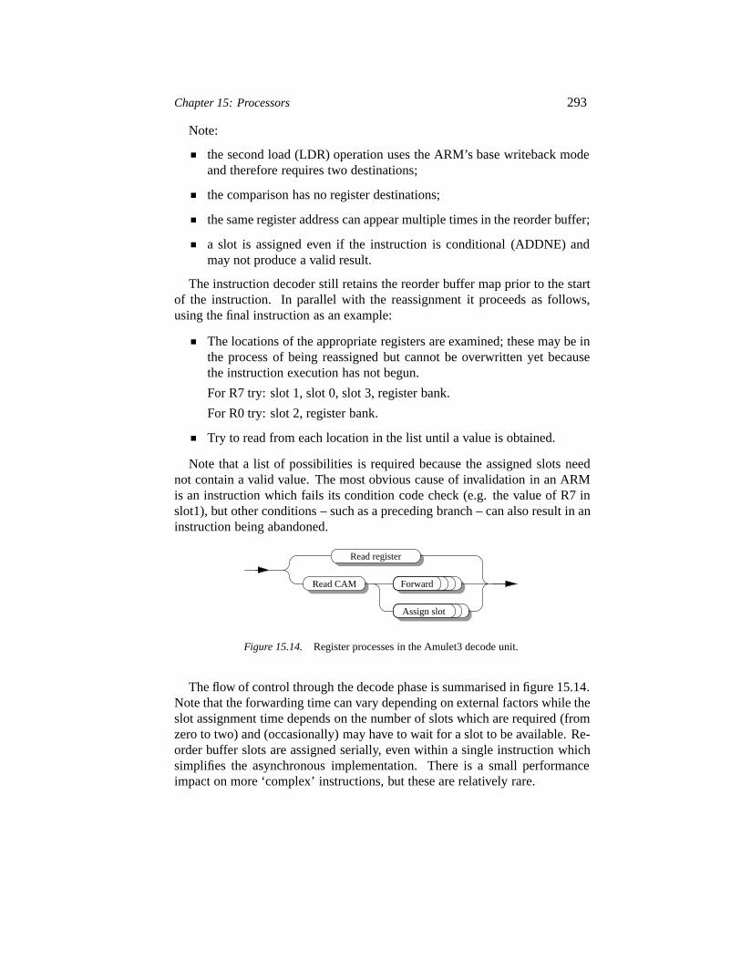
Chapter 15: Processors 293
Note:
the second load (LDR) operation uses the ARM’s base writeback modeand therefore requires two destinations;
the comparison has no register destinations;
the same register address can appear multiple times in the reorder buffer;
a slot is assigned even if the instruction is conditional (ADDNE) andmay not produce a valid result.
The instruction decoder still retains the reorder buffer map prior to the startof the instruction. In parallel with the reassignment it proceeds as follows,using the final instruction as an example:
The locations of the appropriate registers are examined; these may be inthe process of being reassigned but cannot be overwritten yet becausethe instruction execution has not begun.
For R7 try: slot 1, slot 0, slot 3, register bank.
For R0 try: slot 2, register bank.
Try to read from each location in the list until a value is obtained.
Note that a list of possibilities is required because the assigned slots neednot contain a valid value. The most obvious cause of invalidation in an ARMis an instruction which fails its condition code check (e.g. the value of R7 inslot1), but other conditions – such as a preceding branch – can also result in aninstruction being abandoned.
Read register
Read CAM Forward
Assign slot
Figure 15.14. Register processes in the Amulet3 decode unit.
The flow of control through the decode phase is summarised in figure 15.14.Note that the forwarding time can vary depending on external factors while theslot assignment time depends on the number of slots which are required (fromzero to two) and (occasionally) may have to wait for a slot to be available. Re-order buffer slots are assigned serially, even within a single instruction whichsimplifies the asynchronous implementation. There is a small performanceimpact on more ‘complex’ instructions, but these are relatively rare.
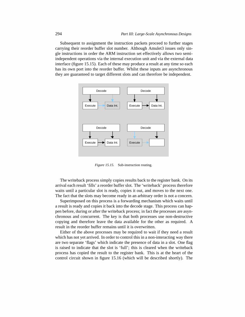
294 Part III: Large-Scale Asynchronous Designs
Subsequent to assignment the instruction packets proceed to further stagescarrying their reorder buffer slot number. Although Amulet3 issues only sin-gle instructions in order the ARM instruction set effectively allows two semi-independent operations via the internal execution unit and via the external datainterface (figure 15.15). Each of these may produce a result at any time so eachhas its own port into the reorder buffer. Whilst these inputs are asynchronousthey are guaranteed to target different slots and can therefore be independent.
LDM − subsequent cycles
Data Load
LDM − first cycle
Internal operation
Decode Decode
Execute
Execute
Data Int.
Decode
Execute
Data Int.
Data Int.
Execute Data Int.
Decode
Figure 15.15. Sub-instruction routing.
The writeback process simply copies results back to the register bank. On itsarrival each result ‘fills’ a reorder buffer slot. The ‘writeback’ process thereforewaits until a particular slot is ready, copies it out, and moves to the next one.The fact that the slots may become ready in an arbitrary order is not a concern.
Superimposed on this process is a forwarding mechanism which waits untila result is ready and copies it back into the decode stage. This process can hap-pen before, during or after the writeback process; in fact the processes are asyn-chronous and concurrent. The key is that both processes use non-destructivecopying and therefore leave the data available for the other as required. Aresult in the reorder buffer remains until it is overwritten.
Either of the above processes may be required to wait if they need a resultwhich has not yet arrived. In order to control this in a non-interacting way thereare two separate ‘flags’ which indicate the presence of data in a slot. One flagis raised to indicate that the slot is ‘full’; this is cleared when the writebackprocess has copied the result to the register bank. This is at the heart of thecontrol circuit shown in figure 15.16 (which will be described shortly). The
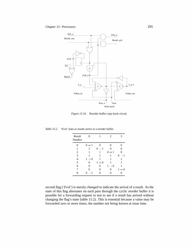
Chapter 15: Processors 295
WPa_nWPr_n
Aout
T_n+1T_n
Rout_n
CC
Match
Try
Fcol
C
Result_ack
Full_n
Token_out
Result_req
Token_in
Write back
Figure 15.16. Reorder buffer copy-back circuit.
Table 15.2. ‘Fcol’ state as results arrive in a reorder buffer.
Result 0 1 2 3Number
0 0� 1 0 0 01 1 0� 1 0 02 1 1 0� 1 03 1 1 1 0� 14 1� 0 1 1 15 0 1� 0 1 16 0 0 1� 0 17 0 0 0 1� 08 0� 1 0 0 0
second flag (‘Fcol’) is merelychanged to indicate the arrival of a result. As thestate of this flag alternates on each pass through the cyclic reorder buffer it ispossible for a forwarding request to test to see if a result has arrived withoutchanging the flag’s state (table 15.2). This is essential because a value may beforwarded zero or more times, the number not being known at issue time.
296 Part III: Large-Scale Asynchronous Designs
As a final embellishment a result returned to the reorder buffer may be in-valid (due, for example, to a condition code failure). Each slot is thereforeaccompanied by a flag which can prevent the data being written to the registerbank (the ‘full’ flag is still cleared) or being forwarded. In the latter case fur-ther forwarding may be attempted from a less recent result, culminating in theuse of the default register value.
The writeback circuit (figure 15.16) is a good example of the working ofsuch asynchronous control circuits. It operates as follows.
The arrival of a result (top left) causes the ‘Full’ bit to be set and ac-knowledges itself (top right). The request comes from one of a numberof mutually exclusive sources.
This event also toggles the forwarding colour (‘Fcol’) which allows anyinstructions issued subsequent to this one to use the result.
Note that the input can be on any of the mutually exclusive input chan-nels; two are shown here but more are possible.
The input request can be removed at any time leaving the slot marked as‘Full’.
When it becomes this slot’s turn to copy back a token is received (bot-tom left) which initiates an output request (bottom centre). If the tokenis received first the circuit waits for the result to arrive. The token isacknowledged.
This process also allows the ‘Full’ bit to be reset, waiting for the inputrequest to fall if it has not already done so.
When the copy back is complete the (broadcast) acknowledge is pickedup by the circuit to complete the token input handshake and pass thetoken to the next, similar circuit to the right. The next slot cannot attemptto output until the four-phase output acknowledge is complete.
These slots are connected in a ring and reset so that there is a single tokenpresent for the first stage to output after which it runs freely, emptying eachslot in turn when it contains a result.
The experimental (and often unsystematic!) way in which Amulet3 was de-signed meant that the original state machine was defined and refined to a ver-sion close to that shown in figure 15.16 as a schematic and only subsequentlysubjected to a more formal analysis. The analysis was carried out using Petrify(which was introduced in section 6.7 on page 102).
At first this caused problems due to the choices within the system. Theoutput channel ‘calls’ the register bank and it was expedient to broadcast theoutput acknowledge to all the copy back circuits and use the (unique) active
Chapter 15: Processors 297
request to sensitize the relevant location. This proved hard to model in a sin-gle subcircuit. However on a suggestion from one of the Petrify developers(Alex Yakovlev) it proved easier to model the whole system than a single part.The resultant signal transition graph (STG) (see figure 15.17) clearly shows thefour implemented subcircuits which pass control around cyclically. The rest ofthe processor is abstracted in the four small rings which, when an output hand-shake has been completed, can reset the circuit to ‘Full’ again at an arbitrarytime.
The analysis with Petrify both verified the circuit’s operation and removeda redundant transistor in each subcircuit.
There are two hazards in the asynchronous processes as described here. Thefirst is that there is no local way of preventing a slot being overwritten beforeit has been emptied. In Amulet3 this is guaranteed elsewhere by ensuring thata slot is never assigned until it has been freed by the copy back process. Ineffect a count of free slots is maintained which is decremented when a slot isassigned and incremented when it is released again. Because assignment andrelease are both cyclic and in-order it is not necessary to pass individual slotidentification, the presence of a token is adequate. This ‘throttle’ is imple-mented as a simple, dataless FIFO which also acts as an asynchronous bufferbetween the unsynchronized processes. This is shown in figure 15.18 for asystem with four reorder buffer slots; in the state shown one result has beenproduced but not yet committed to the register bank, two more are being gen-erated and the decoder could issue another instruction which generated a singleresult.
The other hazard is because the forwarding and writeback processes are notsynchronised, therefore the register value which is read (as a default) could bechanged during the read process, resulting in ‘random’ data being read. How-ever this can only happen if there is a valid value for that register in the reorderbuffer and therefore it is certain that this value will be forwarded in preferenceto the register contents. Providing that the implementor can ensure that the‘random’ data does not cause problems within the circuit, the mechanism issecure against this asynchronous interaction.
Studies of ARM code indicated that for the Amulet3 architecture a reorderbuffer with five or more entries was unlikely ever to fill [50]. Amulet3 thereforeimplements a four entry buffer; however the mechanism described is extensibleto any chosen size.
15.4.5 Exceptions
An ‘exception’ is an unexpected event which occurs in the course of runninga programme. The Amulet processors are compatible with the ARM instruc-
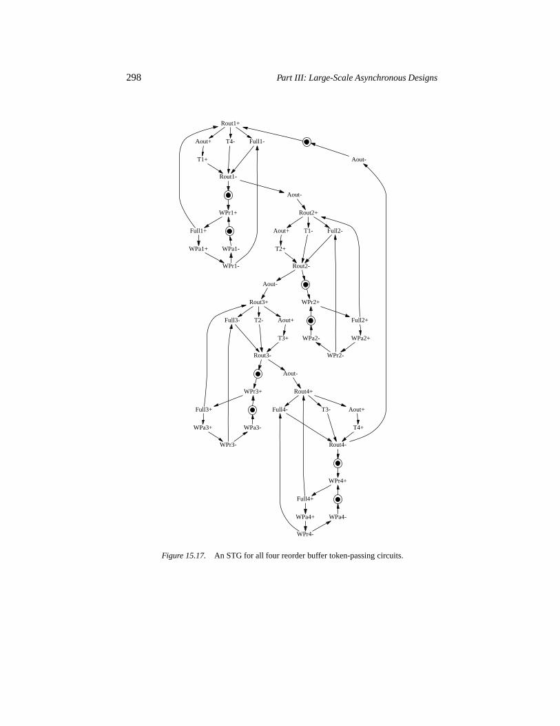
298 Part III: Large-Scale Asynchronous Designs
Rout1+
Full1-T4-Aout+
Rout1-
T1+ Aout-
Aout-
WPr1+ Rout2+
Full1+ Full2-T1-Aout+
WPa1+
Rout2-
T2+
WPr1-
WPa1-
Aout-
WPr2+Rout3+
Full2+Full3- T2- Aout+
WPa2+
Rout3-
T3+
WPr2-
WPa2-
Aout-
WPr3+ Rout4+
Full3+ Full4- T3- Aout+
WPa3+
Rout4-
T4+
WPr3-
WPa3-
WPr4+
Full4+
WPa4+
WPr4-
WPa4-
Figure 15.17. An STG for all four reorder buffer token-passing circuits.
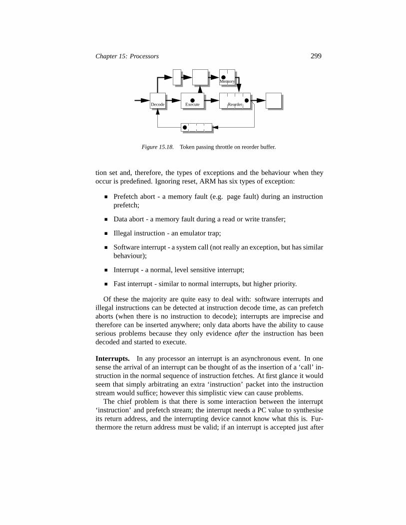
Chapter 15: Processors 299
ExecuteDecode
Memory
Reorder
Figure 15.18. Token passing throttle on reorder buffer.
tion set and, therefore, the types of exceptions and the behaviour when theyoccur is predefined. Ignoring reset, ARM has six types of exception:
Prefetch abort - a memory fault (e.g. page fault) during an instructionprefetch;
Data abort - a memory fault during a read or write transfer;
Illegal instruction - an emulator trap;
Software interrupt - a system call (not really an exception, but has similarbehaviour);
Interrupt - a normal, level sensitive interrupt;
Fast interrupt - similar to normal interrupts, but higher priority.
Of these the majority are quite easy to deal with: software interrupts andillegal instructions can be detected at instruction decode time, as can prefetchaborts (when there is no instruction to decode); interrupts are imprecise andtherefore can be inserted anywhere; only data aborts have the ability to causeserious problems because they only evidenceafter the instruction has beendecoded and started to execute.
Interrupts. In any processor an interrupt is an asynchronous event. In onesense the arrival of an interrupt can be thought of as the insertion of a ‘call’ in-struction in the normal sequence of instruction fetches. At first glance it wouldseem that simply arbitrating an extra ‘instruction’ packet into the instructionstream would suffice; however this simplistic view can cause problems.
The chief problem is that there is some interaction between the interrupt‘instruction’ and prefetch stream; the interrupt needs a PC value to synthesiseits return address, and the interrupting device cannot know what this is. Fur-thermore the return address must be valid; if an interrupt is accepted just after
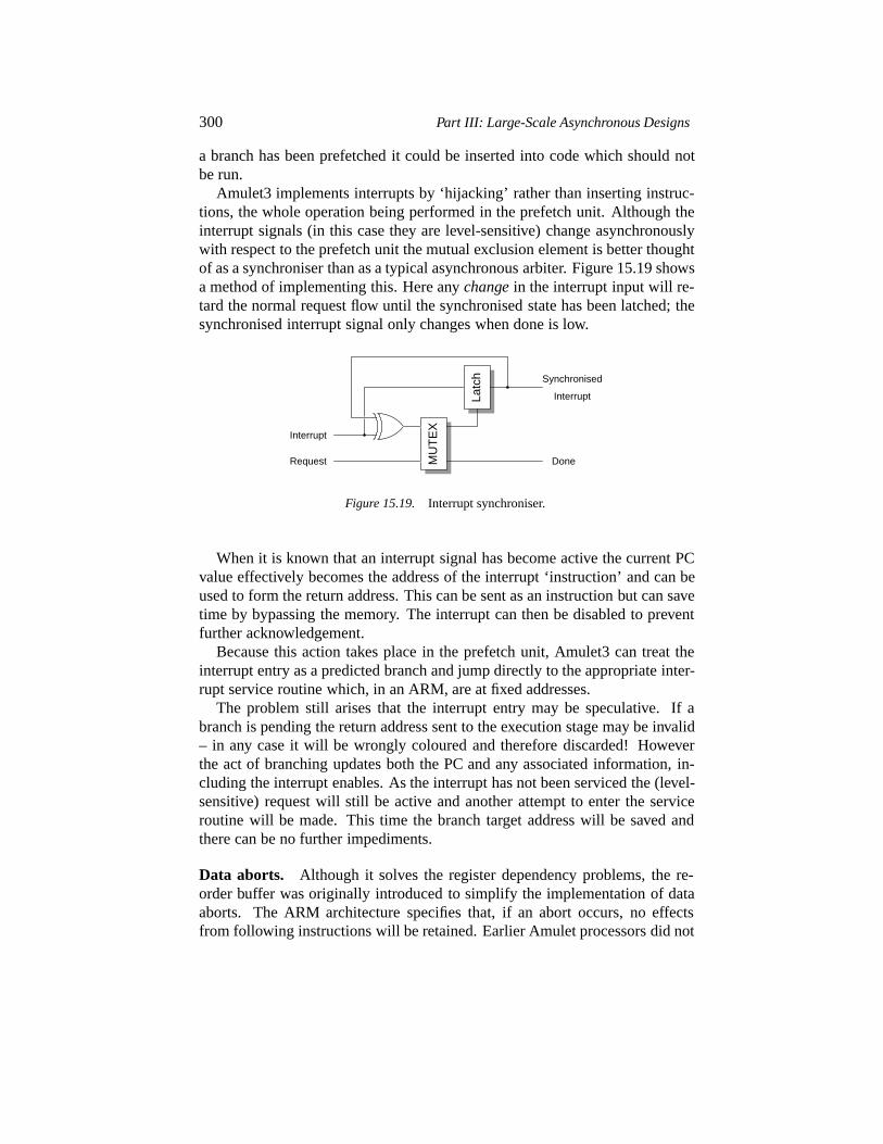
300 Part III: Large-Scale Asynchronous Designs
a branch has been prefetched it could be inserted into code which should notbe run.
Amulet3 implements interrupts by ‘hijacking’ rather than inserting instruc-tions, the whole operation being performed in the prefetch unit. Although theinterrupt signals (in this case they are level-sensitive) change asynchronouslywith respect to the prefetch unit the mutual exclusion element is better thoughtof as a synchroniser than as a typical asynchronous arbiter. Figure 15.19 showsa method of implementing this. Here anychange in the interrupt input will re-tard the normal request flow until the synchronised state has been latched; thesynchronised interrupt signal only changes when done is low.
Request MU
TE
XInterrupt
Interrupt
Synchronised
Done
Latc
h
Figure 15.19. Interrupt synchroniser.
When it is known that an interrupt signal has become active the current PCvalue effectively becomes the address of the interrupt ‘instruction’ and can beused to form the return address. This can be sent as an instruction but can savetime by bypassing the memory. The interrupt can then be disabled to preventfurther acknowledgement.
Because this action takes place in the prefetch unit, Amulet3 can treat theinterrupt entry as a predicted branch and jump directly to the appropriate inter-rupt service routine which, in an ARM, are at fixed addresses.
The problem still arises that the interrupt entry may be speculative. If abranch is pending the return address sent to the execution stage may be invalid– in any case it will be wrongly coloured and therefore discarded! Howeverthe act of branching updates both the PC and any associated information, in-cluding the interrupt enables. As the interrupt has not been serviced the (level-sensitive) request will still be active and another attempt to enter the serviceroutine will be made. This time the branch target address will be saved andthere can be no further impediments.
Data aborts. Although it solves the register dependency problems, the re-order buffer was originally introduced to simplify the implementation of dataaborts. The ARM architecture specifies that, if an abort occurs, no effectsfrom following instructions will be retained. Earlier Amulet processors did not
Chapter 15: Processors 301
speculate on memory operations, relying on a fast ‘go/no go’ decision fromany memory management unit. Amulet3 allows for more sophisticated (i.e.slower!) memory management by outputting memory transfer requests andonly checking for aborts at the end of the operation. To be of any worth thismust allow other, speculative operations to take place in parallel, but theseoperations cannot be ‘retired’ until the outcome of the load is known.
The reorder buffer provides a place for speculative results to be held – andforwarded for reuse if necessary – until they can be retired into registers. In the(rare) case of a data abort the speculative results can be discarded, leaving theregister bank intact. The discard can be achieved either by using a colouringscheme, tested by the register writeback process, or by marking speculativeresults as invalid using the same flag as an operation which has failed for otherreasons. For certain reasons of implementational expediency Amulet3 usesthe latter method, although the asynchronous hazard of invalidating a resultwhilst a forwarding operation is being attempted must be avoided. (This isachieved by implementing two validity bits and nullifying only one of them;the copy back process uses an AND of these whereas forwarding uses an OR.Forwarding is therefore not disturbed, although the result will be discardedlater.)
The reorder buffer accounts only for the register state however; the ARMholds other state bits which also require preservation. Two separate mecha-nisms are used for these, depending on the frequency of changes.
The first is the current programme status register (CPSR) which holds theprocessor’s flags, operating mode et alia, the whole of which can be repre-sented in ten bits. The flags clearly change frequently during execution andthere are many dependences on these bits due, for example, to compare-branchsequences. When attempting a memory operation Amulet3 simply copies thecurrent CPSR state into a history buffer [66] FIFO; successful completion ofthe transaction discards this entry, but an abort can restore the CPSR state tothat at the start of the failed operation.
The other non-register state is a set of five saved programme status regis-ters (SPSRs) which act as a temporary store for the CPSR in various exceptionentries. These change very rarely and it is uneconomic to enlarge the historybuffer to encompass them, although – in theory – they could be changed be-tween a load being issued and an abort being signalled. The solution here wassimply to use a semaphore to lock the SPSRs whilst any memory operationsare outstanding. This delivers the required functionality very cheaply and theperformance penalty is tiny because SPSRs change so rarely.
302 Part III: Large-Scale Asynchronous Designs
15.5. Memory – a case study
It seems reasonable that an asynchronous processor should interact with anasynchronous memory system. This implies the need for handshake interfaceson a range of memory systems, including RAM, ROM and caches. This is thesubject of the following sections.
An individual memory array is a very regular structure and – under steadyvoltage, temperature etc. conditions – will produce data in a constant time.At first glance this may suggest that there is not much scope for asynchronousdesign within a memory system. However each part of the memory will haveits own characteristic timing; in some cases even a simple memory will have avariable cycle time. An example is a RAM which will typically take longer toread from than it will to write to.
In fact the memory system is one part of a computer which has extremelyvariable timing; even a clocked computer will take different times to service acache hit and a cache miss. An asynchronous system will accommodate suchcycle time variation quite naturally and is able to exploit many more subtlevariations which would be padded to fill a clock cycle in a synchronous ma-chine.
15.5.1 Sequential accesses
A static RAM (SRAM) stores data in small flip-flops which have only avery weak output drive. To accelerate read access it is normal to use ‘senseamplifiers’ to detect small (sub-digital) swings in voltage and produce an earlydigital output. Sense amplifiers, being analogue parts, are quite power-hungry.
Sense amplification is only useful when there has been enough voltageswing for the read bits to be discriminated; it is also only required until thebits can be latched. As this period is certainly less than even half a clock cyclethis is an ideal application for a self-timed system. A delay can be inserted tokeep the sense amplifiers ‘switched off’ when the read cycle commences andonly switch them on when they may be useful. An extra (known) bit in theRAM may then be discriminated and, when it has been read, used to latch theentire RAM line and disable the sense amplifiers. The same signal can be usedto indicate the completion of the read cycle, possibly returning the RAM arrayto the precharge state in preparation for another cycle (figure 15.20).
When designing such a circuit the RAM completion is easy to detect but thedelay before enabling the sense amplifiers is harder to judge. The designer canchoose this to be short – to ensure maximum speed – or somewhat longer –to ensure the memory is ready before the amplifiers are enabled thus ensuringminimum power wastage. If the designer errs then either speed or power maybe compromised slightly, however functionality is retained.
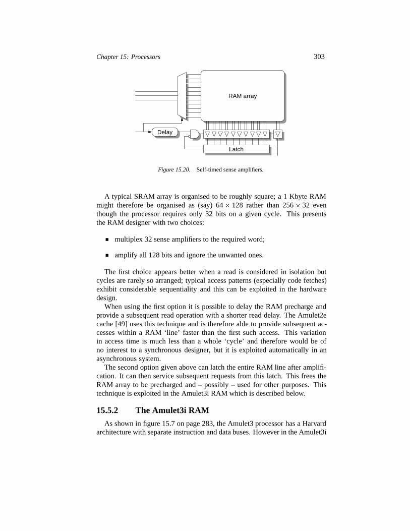
Chapter 15: Processors 303
Delay
RAM array
Latch
Figure 15.20. Self-timed sense amplifiers.
A typical SRAM array is organised to be roughly square; a 1 Kbyte RAMmight therefore be organised as (say) 64� 128 rather than 256� 32 eventhough the processor requires only 32 bits on a given cycle. This presentsthe RAM designer with two choices:
multiplex 32 sense amplifiers to the required word;
amplify all 128 bits and ignore the unwanted ones.
The first choice appears better when a read is considered in isolation butcycles are rarely so arranged; typical access patterns (especially code fetches)exhibit considerable sequentiality and this can be exploited in the hardwaredesign.
When using the first option it is possible to delay the RAM precharge andprovide a subsequent read operation with a shorter read delay. The Amulet2ecache [49] uses this technique and is therefore able to provide subsequent ac-cesses within a RAM ‘line’ faster than the first such access. This variationin access time is much less than a whole ‘cycle’ and therefore would be ofno interest to a synchronous designer, but it is exploited automatically in anasynchronous system.
The second option given above can latch the entire RAM line after amplifi-cation. It can then service subsequent requests from this latch. This frees theRAM array to be precharged and – possibly – used for other purposes. Thistechnique is exploited in the Amulet3i RAM which is described below.
15.5.2 The Amulet3i RAM
As shown in figure 15.7 on page 283, the Amulet3 processor has a Harvardarchitecture with separate instruction and data buses. However in the Amulet3i
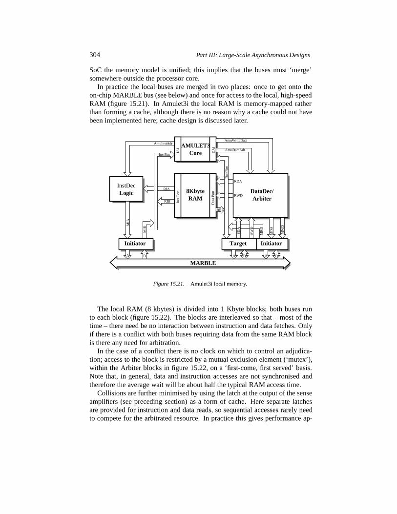
304 Part III: Large-Scale Asynchronous Designs
SoC the memory model is unified; this implies that the buses must ‘merge’somewhere outside the processor core.
In practice the local buses are merged in two places: once to get onto theon-chip MARBLE bus (see below) and once for access to the local, high-speedRAM (figure 15.21). In Amulet3i the local RAM is memory-mapped ratherthan forming a cache, although there is no reason why a cache could not havebeen implemented here; cache design is discussed later.
A D
AmuInstAdr
InstBus
RIA
MID
RRI
Dat
a P
ort
Inst
Por
t
Dat
aBus
AmuWriteData
AmuDataAdr
SD
A
A D A D
Initiator
LogicInstDec
CoreAMULET3
DataDec/Arbiter
Target Initiator
8KbyteRAM
MIA
RRD
RDA
RWD
SW
D
MR
D
MD
A
MW
D
MARBLE
DA
I
IAI
Figure 15.21. Amulet3i local memory.
The local RAM (8 kbytes) is divided into 1 Kbyte blocks; both buses runto each block (figure 15.22). The blocks are interleaved so that – most of thetime – there need be no interaction between instruction and data fetches. Onlyif there is a conflict with both buses requiring data from the same RAM blockis there any need for arbitration.
In the case of a conflict there is no clock on which to control an adjudica-tion; access to the block is restricted by a mutual exclusion element (‘mutex’),within the Arbiter blocks in figure 15.22, on a ‘first-come, first served’ basis.Note that, in general, data and instruction accesses are not synchronised andtherefore the average wait will be about half the typical RAM access time.
Collisions are further minimised by using the latch at the output of the senseamplifiers (see preceding section) as a form of cache. Here separate latchesare provided for instruction and data reads, so sequential accesses rarely needto compete for the arbitrated resource. In practice this gives performance ap-
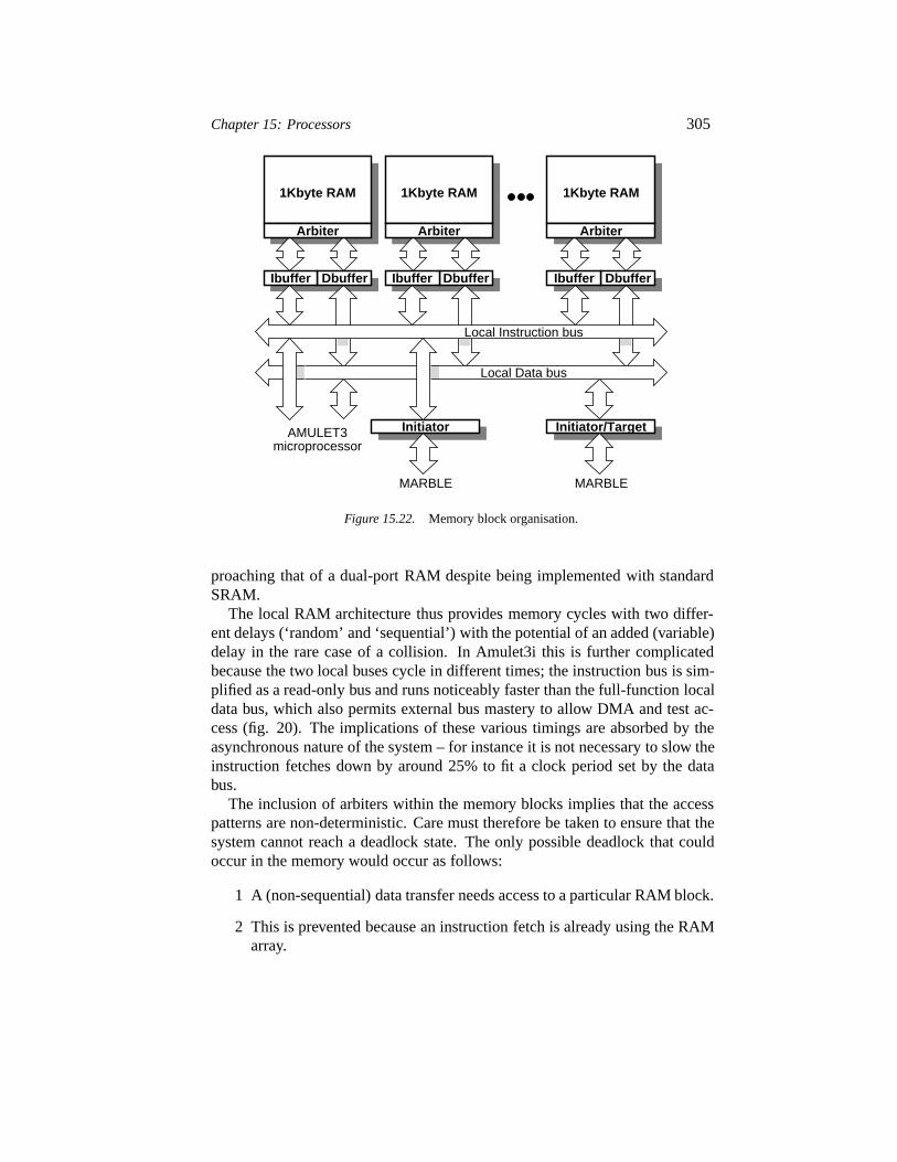
Chapter 15: Processors 305
Arbiter Arbiter Arbiter
Initiator Initiator/Target
Dbuffer Ibuffer Dbuffer IbufferIbuffer Dbuffer
MARBLE
Local Instruction bus
Local Data bus
MARBLE
microprocessorAMULET3
1Kbyte RAM1Kbyte RAM1Kbyte RAM
Figure 15.22. Memory block organisation.
proaching that of a dual-port RAM despite being implemented with standardSRAM.
The local RAM architecture thus provides memory cycles with two differ-ent delays (‘random’ and ‘sequential’) with the potential of an added (variable)delay in the rare case of a collision. In Amulet3i this is further complicatedbecause the two local buses cycle in different times; the instruction bus is sim-plified as a read-only bus and runs noticeably faster than the full-function localdata bus, which also permits external bus mastery to allow DMA and test ac-cess (fig. 20). The implications of these various timings are absorbed by theasynchronous nature of the system – for instance it is not necessary to slow theinstruction fetches down by around 25% to fit a clock period set by the databus.
The inclusion of arbiters within the memory blocks implies that the accesspatterns are non-deterministic. Care must therefore be taken to ensure that thesystem cannot reach a deadlock state. The only possible deadlock that couldoccur in the memory would occur as follows:
1 A (non-sequential) data transfer needs access to a particular RAM block.
2 This is prevented because an instruction fetch is already using the RAMarray.
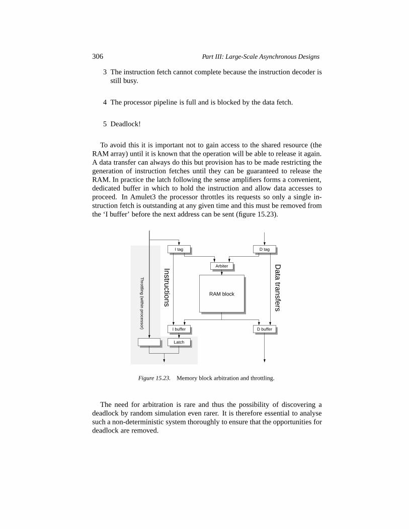
306 Part III: Large-Scale Asynchronous Designs
3 The instruction fetch cannot complete because the instruction decoder isstill busy.
4 The processor pipeline is full and is blocked by the data fetch.
5 Deadlock!
To avoid this it is important not to gain access to the shared resource (theRAM array) until it is known that the operation will be able to release it again.A data transfer can always do this but provision has to be made restricting thegeneration of instruction fetches until they can be guaranteed to release theRAM. In practice the latch following the sense amplifiers forms a convenient,dedicated buffer in which to hold the instruction and allow data accesses toproceed. In Amulet3 the processor throttles its requests so only a single in-struction fetch is outstanding at any given time and this must be removed fromthe ‘I buffer’ before the next address can be sent (figure 15.23).
Latch Latch
Arbiter
D tag
D buffer
I tag
I buffer
Instructions
Data transfers
Throttling (w
ithin processor)
RAM block
Figure 15.23. Memory block arbitration and throttling.
The need for arbitration is rare and thus the possibility of discovering adeadlock by random simulation even rarer. It is therefore essential to analysesuch a non-deterministic system thoroughly to ensure that the opportunities fordeadlock are removed.
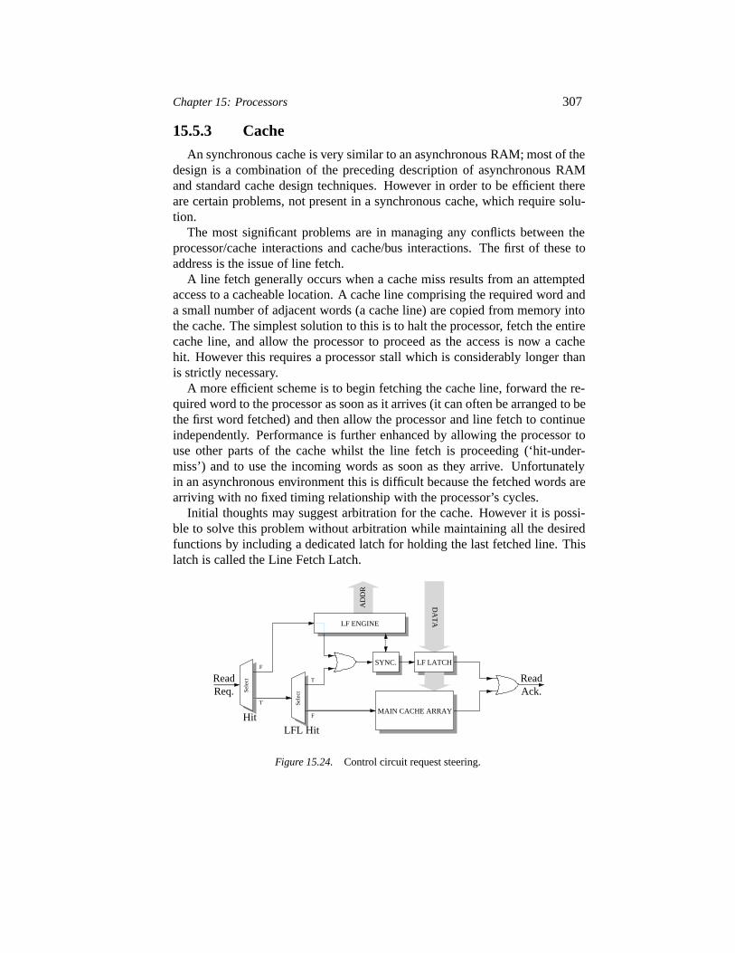
Chapter 15: Processors 307
15.5.3 Cache
An synchronous cache is very similar to an asynchronous RAM; most of thedesign is a combination of the preceding description of asynchronous RAMand standard cache design techniques. However in order to be efficient thereare certain problems, not present in a synchronous cache, which require solu-tion.
The most significant problems are in managing any conflicts between theprocessor/cache interactions and cache/bus interactions. The first of these toaddress is the issue of line fetch.
A line fetch generally occurs when a cache miss results from an attemptedaccess to a cacheable location. A cache line comprising the required word anda small number of adjacent words (a cache line) are copied from memory intothe cache. The simplest solution to this is to halt the processor, fetch the entirecache line, and allow the processor to proceed as the access is now a cachehit. However this requires a processor stall which is considerably longer thanis strictly necessary.
A more efficient scheme is to begin fetching the cache line, forward the re-quired word to the processor as soon as it arrives (it can often be arranged to bethe first word fetched) and then allow the processor and line fetch to continueindependently. Performance is further enhanced by allowing the processor touse other parts of the cache whilst the line fetch is proceeding (‘hit-under-miss’) and to use the incoming words as soon as they arrive. Unfortunatelyin an asynchronous environment this is difficult because the fetched words arearriving with no fixed timing relationship with the processor’s cycles.
Initial thoughts may suggest arbitration for the cache. However it is possi-ble to solve this problem without arbitration while maintaining all the desiredfunctions by including a dedicated latch for holding the last fetched line. Thislatch is called the Line Fetch Latch.
ReadF
ReadAck.
Sel
ect
T
F
Sel
ect
LFL Hit
SYNC. LF LATCH
MAIN CACHE ARRAY
Req.
Hit
T
DA
TALF ENGINE
AD
DR
Figure 15.24. Control circuit request steering.
308 Part III: Large-Scale Asynchronous Designs
The line fetch latch (LFL) (figure 15.24) is actually a set of latches residingjust outside the true RAM array. It normally holds the last-fetched cache line.It has its own tag and comparator which allow it to function much like the othercache lines. Note that the LFL holds the only copy of this data. (Incidentally,because the LFL is static and requires no sense amplification when it is read itcan provide faster access in an asynchronous system.)
When, as a result of a cache miss, a fetch is needed, a line from the RAM isselected for rejection. For the moment assume that the cache is write-throughand therefore the RAM can simply be overwritten. The LFL contents, togetherwith its tag, are then copied into the chosen line and the LFL is marked as‘empty’. This can happen in parallel with the start of the external access.
The processor is then assumed to have a cache hit from within the LFL andattempts to read the appropriate word; this causes a stall at the synchronisationpoint because the word is empty and – unless the external memory is excep-tionally fast – will not have been refilled yet.
As words arrive they are stored in the LFL and individually flagged as ‘full’.As soon as the processor can read a word from the LFL (typically after thecompletion of the first fetch cycle) it can continue. From this time the processorcan continue in parallel with the remaining words being fetched.
A subsequent cache cycle could be:
a cache hit: this can proceed independently and without interaction withthe LFL;
a cache miss: this will cause a stall until the line fetch process is com-plete and the fetch process can be repeated;
a LFL hit: this attempts to read the LFL whilst it is being filled. Thepossibilities are that the required word is already present (the processorcontinues) or the word is still pending (the processor must stall until itarrives.
Only in the last case is there any interaction between the asynchronous pro-cesses. However this interaction is merely a wait which can be implementedwith a flip-flop and an AND gate (figure 15.25). The potential wait beginswhen the LFL is first emptied (caused by, and therefore synchronised with,the processor’s action). The wait can end at an arbitrary time but this merelydelays a transition; it cannot abort or change an action and can therefore beimplemented without arbitration or the risk of metastability. This mechanismwas first implemented in the Amulet2e cache system [49] and was also used inTITAC-2 [130].
Both these processors used a simple write-through cache for simplicity. Forhigher performance a copy-back mechanism is needed. This too can be pro-vided using an extension of the LFL mechanism. In this case the process of
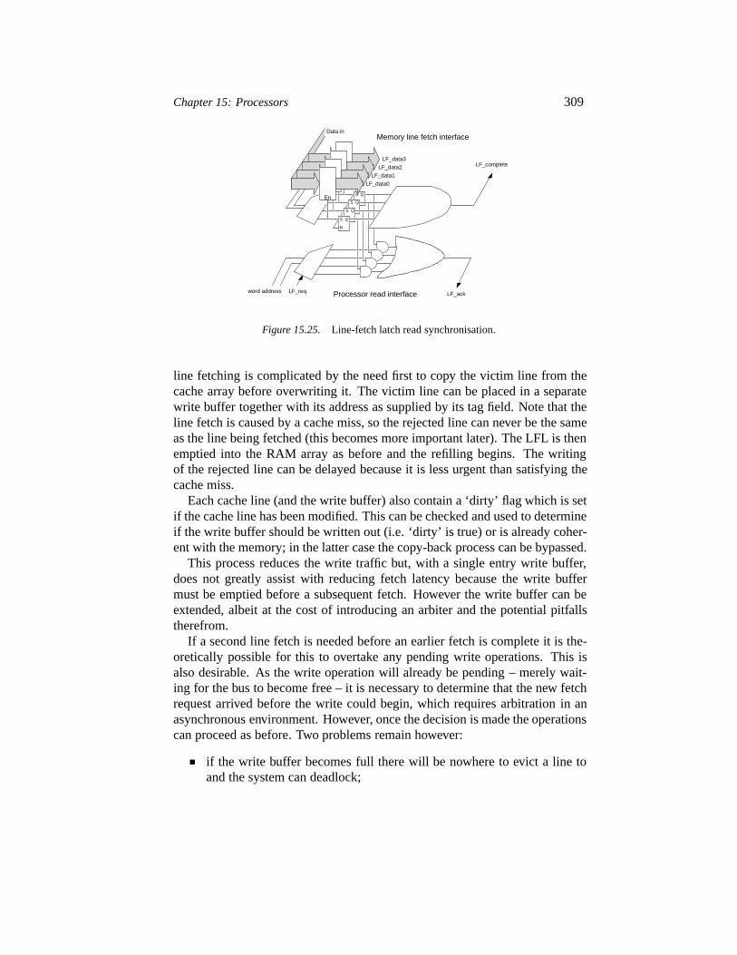
Chapter 15: Processors 309
Q
R
S
QS
Q
R
S
Q
R
S
Memory line fetch interface
LF_data3
LF_data2
LF_data1
LF_data0
En
Data in
word address LF_req Processor read interface
LF_complete
LF_ack
Figure 15.25. Line-fetch latch read synchronisation.
line fetching is complicated by the need first to copy the victim line from thecache array before overwriting it. The victim line can be placed in a separatewrite buffer together with its address as supplied by its tag field. Note that theline fetch is caused by a cache miss, so the rejected line can never be the sameas the line being fetched (this becomes more important later). The LFL is thenemptied into the RAM array as before and the refilling begins. The writingof the rejected line can be delayed because it is less urgent than satisfying thecache miss.
Each cache line (and the write buffer) also contain a ‘dirty’ flag which is setif the cache line has been modified. This can be checked and used to determineif the write buffer should be written out (i.e. ‘dirty’ is true) or is already coher-ent with the memory; in the latter case the copy-back process can be bypassed.
This process reduces the write traffic but, with a single entry write buffer,does not greatly assist with reducing fetch latency because the write buffermust be emptied before a subsequent fetch. However the write buffer can beextended, albeit at the cost of introducing an arbiter and the potential pitfallstherefrom.
If a second line fetch is needed before an earlier fetch is complete it is the-oretically possible for this to overtake any pending write operations. This isalso desirable. As the write operation will already be pending – merely wait-ing for the bus to become free – it is necessary to determine that the new fetchrequest arrived before the write could begin, which requires arbitration in anasynchronous environment. However, once the decision is made the operationscan proceed as before. Two problems remain however:
if the write buffer becomes full there will be nowhere to evict a line toand the system can deadlock;
310 Part III: Large-Scale Asynchronous Designs
if the required line is one which has recently been evicted the fetch couldovertake a pending write and thus lose cache coherency.
The first problem is relatively easy to solve; a simple counter can ensurethat only a certain amount of overtaking is allowed and that one space in thewrite buffer always remains free (i.e. when the last entry is filled the next busoperation must be a write – unless, of course, it is a ‘clean’ line where the writecan be assumed and bypassed). This can be implemented, for example, as asemaphore.
The second problem is harder, but can be solved by forwarding in a similarmanner to the forwarding from a processor’s reorder buffer. A line fetch checksthe addresses of the entries in the write buffer and, if it finds a match, satisfiesitself from there instead of requesting the memory bus. In such a case the‘fetch’ can be performed with no latency, much more rapidly as it is an internaloperation and can copy an entire cache line in a single operation. This is, ofcourse, irrelevant to the functioning of other parts of the system as the wholeis self-timed anyway. Such forwarding does not affect the write process (a re-fetched ‘dirty’ line is returned clean) and can take place regardless of whetherthe copy-back is pending, in progress, complete or not needed. The write bufferacts, in effect, as a write-through victim cache [56].
There is one caveat to this process; the line fetch occurs in parallel withthe eviction of a cache line. It is therefore possible that one entry in the writebuffer could be changingduring the comparison process. As noted above thisentry is reserved for the freshly evicted line and can safely be excluded fromthe comparison, thus averting any possibilities of a false positive due to signalschanging.
15.6. Larger asynchronous systems
15.6.1 System-on-Chip (DRACO)
DRACO (DECT Radio Communications Controller) (figure 15.26) is a sys-tem on chip based around the Amulet3 processor. In terms of area about halfof the (7 mm square) device is an asynchronous ‘island’ – hence Amulet3i –and the other half comprises synchronous peripherals compiled from VHDL.
The asynchronous subsystem (figure 15.27) is a computer in itself and wasdeveloped both with commercial intent and with a view to investigating somenew techniques. The processor and RAM have already been discussed. Someother novel asynchronous features are outlined in this section.
15.6.2 Interconnection
Ideally an asynchronous system should be based around an asynchronousbus. Indeed it is arguable that large, fast synchronous systems should also use
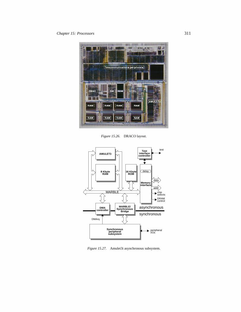
Chapter 15: Processors 311
Figure 15.26. DRACO layout.
subsystem
8 Kbyte
interfaceTest
interfaceMemory
BridgeSynchronous
MARBLE/
peripheral
DMA
I/Osperipheral
controlDRAM
selects
ROM
chip
controller
Synchronous
controller
RAM16 Kbyte
data
addr
DMArq
test
delay
AMULET3
MARBLE
synchronous
asynchronous
Figure 15.27. Amulet3i asynchronous subsystem.
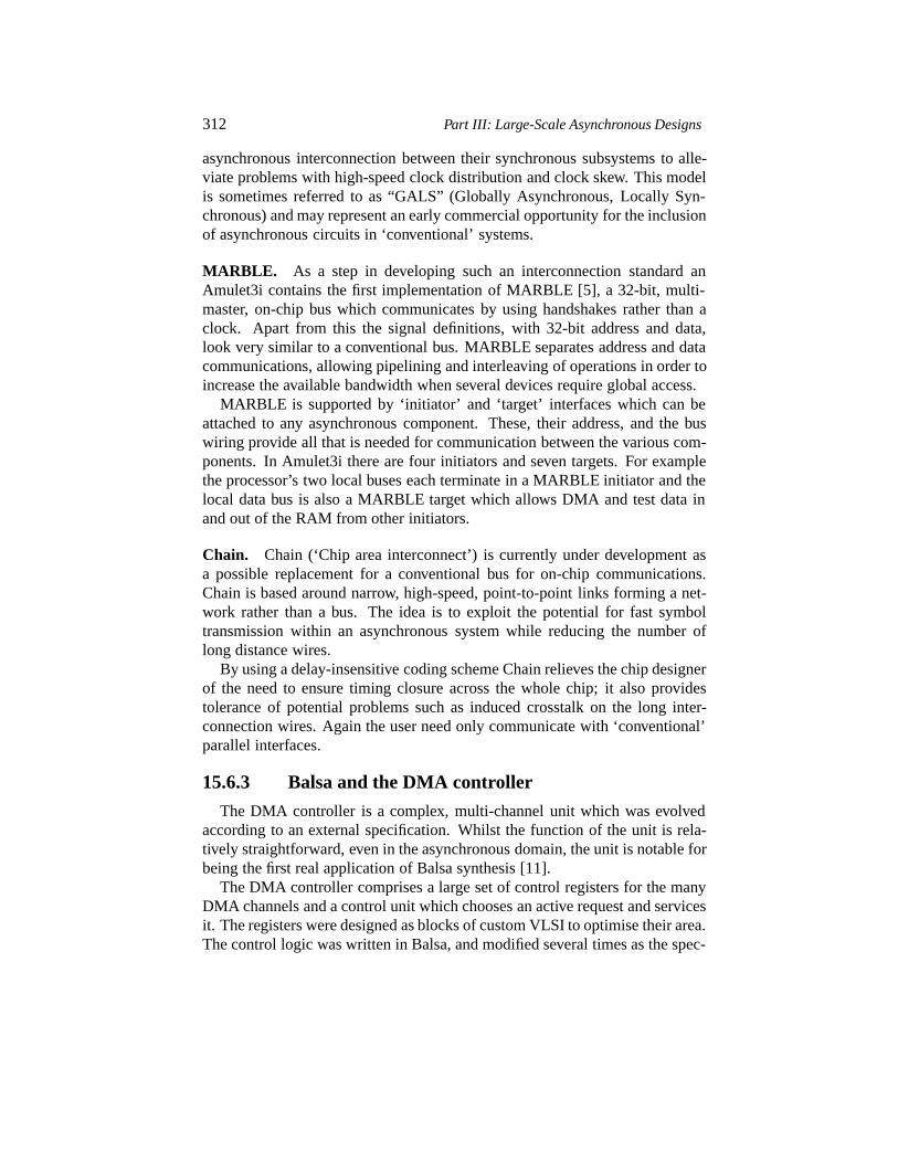
312 Part III: Large-Scale Asynchronous Designs
asynchronous interconnection between their synchronous subsystems to alle-viate problems with high-speed clock distribution and clock skew. This modelis sometimes referred to as “GALS” (Globally Asynchronous, Locally Syn-chronous) and may represent an early commercial opportunity for the inclusionof asynchronous circuits in ‘conventional’ systems.
MARBLE. As a step in developing such an interconnection standard anAmulet3i contains the first implementation of MARBLE [5], a 32-bit, multi-master, on-chip bus which communicates by using handshakes rather than aclock. Apart from this the signal definitions, with 32-bit address and data,look very similar to a conventional bus. MARBLE separates address and datacommunications, allowing pipelining and interleaving of operations in order toincrease the available bandwidth when several devices require global access.
MARBLE is supported by ‘initiator’ and ‘target’ interfaces which can beattached to any asynchronous component. These, their address, and the buswiring provide all that is needed for communication between the various com-ponents. In Amulet3i there are four initiators and seven targets. For examplethe processor’s two local buses each terminate in a MARBLE initiator and thelocal data bus is also a MARBLE target which allows DMA and test data inand out of the RAM from other initiators.
Chain. Chain (‘Chip area interconnect’) is currently under development asa possible replacement for a conventional bus for on-chip communications.Chain is based around narrow, high-speed, point-to-point links forming a net-work rather than a bus. The idea is to exploit the potential for fast symboltransmission within an asynchronous system while reducing the number oflong distance wires.
By using a delay-insensitive coding scheme Chain relieves the chip designerof the need to ensure timing closure across the whole chip; it also providestolerance of potential problems such as induced crosstalk on the long inter-connection wires. Again the user need only communicate with ‘conventional’parallel interfaces.
15.6.3 Balsa and the DMA controller
The DMA controller is a complex, multi-channel unit which was evolvedaccording to an external specification. Whilst the function of the unit is rela-tively straightforward, even in the asynchronous domain, the unit is notable forbeing the first real application of Balsa synthesis [11].
The DMA controller comprises a large set of control registers for the manyDMA channels and a control unit which chooses an active request and servicesit. The registers were designed as blocks of custom VLSI to optimise their area.The control logic was written in Balsa, and modified several times as the spec-
Chapter 15: Processors 313
ification changed. The modifications proved remarkably easy to accommodatein this environment.
Such synthesis is not (yet) suitable for high-performance units, but provedextremely useful in such an application where the performance was limited byother constraints (such as the bus speed, here) and development time predom-inates. Of course, in an asynchronous environment, it is easy to accommodatedevices in any performance range without affecting the overall system func-tionality.
Part II of this book is an introduction to Balsa and includes a completesource listing of a simpler 4-channel DMA controller.
15.6.4 Calibrated time delays
To be useful in real systems an asynchronous processor must be able tointerface with currently available commodity parts. Whilst it is possible – andperhaps even desirable – to have memory devices with handshake interfaces,these are not available ‘off the shelf’. Instead commodity memories rely onabsolute timing assumptions to guarantee their correct operation and thus asystem using them must have an accurate timing reference. This is the onething lacking in an asynchronous design.
Introducing a clock purely to provide memory timing would negate many ofthe advantages of the asynchronous system; it is therefore preferable to retainthe idea of providing data ‘on demand’, providing an adequately precise delaycan be provided. This delay need not be a clock; a monostable which can betriggered on demand is preferable.
Amulet1 and Amulet2e relied on an externally supplied delay line to pro-vide a bus timing reference. This is a flexible solution in that a short delaycan be used repeatedly to provide longer timing intervals, providing a flexible,programmable interface. For example an area of address space could be setup for DRAM devices with (say) 1 delay address set up time, 2 delays RASaddress hold, etc. The bus interface can then count delays as appropriate.
This is a reasonable solution but suffers from certain drawbacks:
the on-chip delay for each delay cycle is not factored;
delay lines are not particularly precise;
driving an off-chip delay is power hungry.
A much better solution would be to use an on-chip delay. The chief problemwith this is that a fixed delay will be imprecise, varying from chip to chip andalso changing with temperature and supply voltage fluctuations. Any on-boarddelay must therefore be calibratable against an external reference.
Amulet3i uses such a delay. This comprises a chain of delay elements (fig-ure 15.28) which can be ‘shorted’ at a determined point. This can be calibrated
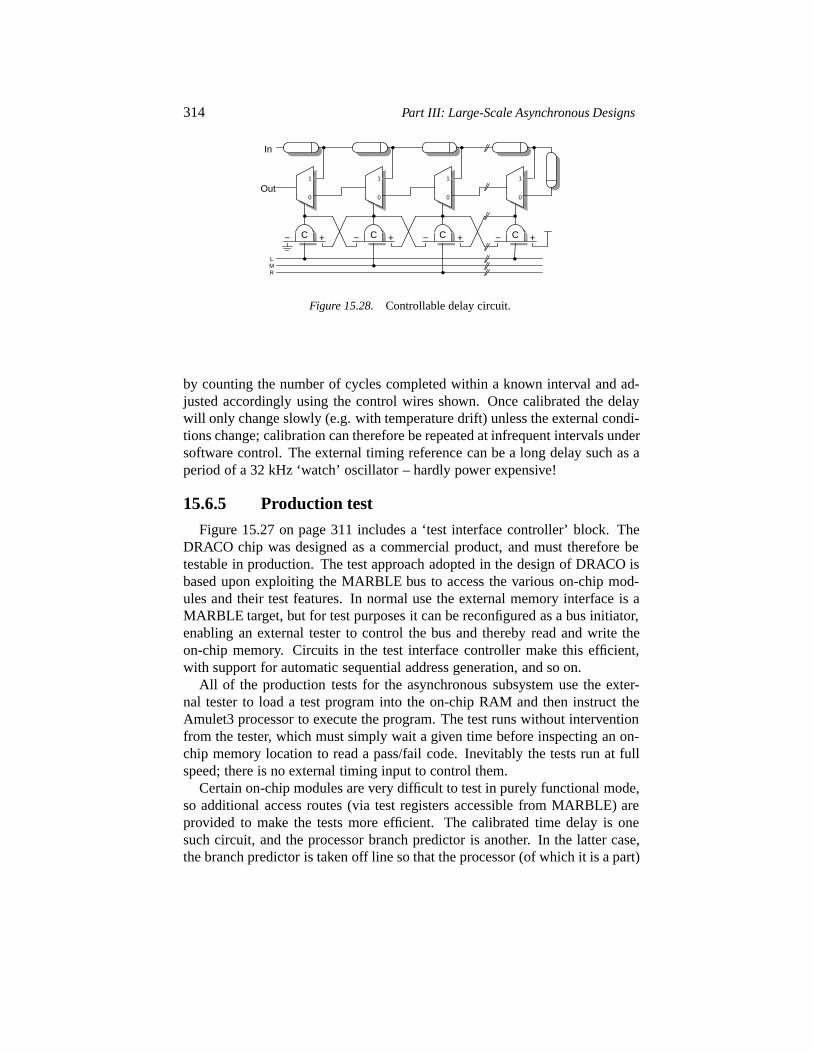
314 Part III: Large-Scale Asynchronous Designs
−
R
C
M
+
Out
−− C
In
C + +−+
L
C
0 0
1
0
11
0
1
Figure 15.28. Controllable delay circuit.
by counting the number of cycles completed within a known interval and ad-justed accordingly using the control wires shown. Once calibrated the delaywill only change slowly (e.g. with temperature drift) unless the external condi-tions change; calibration can therefore be repeated at infrequent intervals undersoftware control. The external timing reference can be a long delay such as aperiod of a 32 kHz ‘watch’ oscillator – hardly power expensive!
15.6.5 Production test
Figure 15.27 on page 311 includes a ‘test interface controller’ block. TheDRACO chip was designed as a commercial product, and must therefore betestable in production. The test approach adopted in the design of DRACO isbased upon exploiting the MARBLE bus to access the various on-chip mod-ules and their test features. In normal use the external memory interface is aMARBLE target, but for test purposes it can be reconfigured as a bus initiator,enabling an external tester to control the bus and thereby read and write theon-chip memory. Circuits in the test interface controller make this efficient,with support for automatic sequential address generation, and so on.
All of the production tests for the asynchronous subsystem use the exter-nal tester to load a test program into the on-chip RAM and then instruct theAmulet3 processor to execute the program. The test runs without interventionfrom the tester, which must simply wait a given time before inspecting an on-chip memory location to read a pass/fail code. Inevitably the tests run at fullspeed; there is no external timing input to control them.
Certain on-chip modules are very difficult to test in purely functional mode,so additional access routes (via test registers accessible from MARBLE) areprovided to make the tests more efficient. The calibrated time delay is onesuch circuit, and the processor branch predictor is another. In the latter case,the branch predictor is taken off line so that the processor (of which it is a part)
Chapter 15: Processors 315
can manipulate its internal state to run optimised tests on its CAM and RAMcomponents.
Although DRACO is not, at the time of writing, in full-scale production, thetests ran without difficulty on prototype sample parts.
15.7. Summary
Devices such as DRACO have demonstrated that it is feasible to build large,functional asynchronous systems. Like any prototype system the chip has itsproblems. There are two (known) bugs in the asynchronous half of the sys-tem: an electrical drive strength problem within the multiplier (which failed toevidence during simulation) and a logic oversight in the prefetch unit whichfalsely indicates a cycle is ‘sequential’ under certain specific conditions (aproblem if running code from off-chip DRAM). Neither of these is attributableto the asynchronous nature of the device (indeed, there are slightly more bugsin the synchronous part of the device!) and both are readily fixable. The pro-cessor is comparable with an ARM9 manufactured on the same process interms of physical size, performance and energy efficiency; preliminary mea-surements suggest that is is significantly ‘quieter’ in terms of EMI.
This chapter has presented possible solutions (though certainly not the onlyones!) to many of the problems facing the designer of complex asynchronousprocessing and memory systems. The majority of the designs described at thebeginning of the chapter have been produced by academic groups and could beclassified as “research”; however the complexity of a modern system on chip issuch that these designs stretch the capability of even a large university group. Ithas been demonstrated that large, functional asynchronous designs are not onlypossible, but can be competitive and have some unique advantages in terms ofpower management and EMI. Asynchronous interconnection may be the onlysolution for large devices, even those with local clocks. Asynchronous chipdesign is ready to move to “development”.

Epilogue
Asynchronous technology has existed since the first days of digital elec-tronics – many of the earliest computers did not employ a central clock signal.However, with the development of integrated circuits the need for a straightfor-ward design discipline that could scale up rapidly with the available transistorresource was pressing, and clocked design became the dominant approach.Today, most practising digital designers know very little about asynchronoustechniques, and what they do know tends to discourage them from venturinginto the territory. But clocked design is beginning to show signs of stress – itsability to scale is waning, and it brings with it growing problems of excessivepower dissipation and electromagnetic interference.
During the reign of the clock, a few designers have remained convinced thatasynchronous techniques have merit, and new techniques have been developedthat are far better suited to the VLSI era than were the approaches employed onearly machines. In this book we have tried to illuminate these new techniquesin a way that is accessible to any practising digital circuit designer, whether ornot they have had prior exposure to asynchronous circuits.
In this account of asynchronous design techniques we have had to be selec-tive in order not to obscure the principal goal with arcane detail. Much work ofconsiderable quality and merit has been omitted, and the reader whose interesthas been ignited by this book will find that there is a great deal of publishedmaterial available that exposes aspects of asynchronous design that have notbeen touched upon here.
Although there are commercial examples of VLSI devices based on asyn-chronous techniques (a couple of which have been described in this book),these are exceptions – most asynchronous development is still taking place inresearch laboratories. If this is to change in the future, where will this changefirst manifest itself?
The impending demise of clocked design has been forecast for many yearsand still has not happened. If it does happen, it will be for some compellingreason, since designers will not lightly cast aside their years of experience inone design style in favour of another style that is less proven and less wellsupported by automated tools.
317
318 PRINCIPLES OF ASYNCHRONOUS DESIGN
There are many possible reasons for considering asynchronous design, butno single ‘killer application’ that makes its use obligatory. Several of the argu-ments for adopting asynchronous techniques mentioned at the start of this book– low power, low electromagnetic interference, modularity, etc. – are applica-ble in their own niches, but only the modularity argument has the potential togain universal adoption. Here a promising approach that will support hetero-geneous timing environments is GALS (Globally Asynhronous Locally Syn-chronous) system design. An asynchronous on-chip interconnect – a ‘chip areanetwork’ such as Chain (described on page 312) – is used to connect clockedmodules. The modules themselves can be kept small enough for clock skew tobe well-contained so that straightforward synchronous design techniques workwell, and different modules can employ different clocks or the same clock withdifferent phases. Once this framework is in place, it is then clearly straightfor-ward to make individual modules asynchronous on a case-by-case basis.
Here, perhaps unsurprisingly, we see the need to merge asynchronous tech-nology with established synchronous design techniques, so most of the func-tional design can be performed using well-understood tools and approaches.This evolutionary approach contrasts with the revolutionary attacks describedin Part III of this book, and represents the most likely scenario for the wide-spread adoption of the techniques described in this book in the medium-termfuture.
In the shorter term, however, the application niches that can benefit fromasynchronous technology are important and viable. It is our hope in writingthis book that more designers will come to understand the principles of asyn-chronous design and its potential to offer new solutions to old and new prob-lems. Clocks are useful but they can become straitjackets. Don’t be afraid tothink outside the box!
For further information on asynchronous design see the bibliography at theend of this book, theAsynchronous Bibliography on the Internet [111], andthe general information on asynchronous design available at theAsynchronousLogic Homepage, also on the Internet [47].
References
[1] G. Abouyannis et al. Project PREST EP25242.European Low PowerInitiative for Electronic System Design (ESDLPD) Third InternationalWorkshop, pages 5–49, 2000.
[2] A. Abrial, J. Bouvier, M. Renaudin, P. Senn, and P. Vivet. A new con-tactless smartcard IC using an on-chip antenna and an asynchronousmicro-controller. IEEE Journal of Solid-State Circuits, 36(7):1101–1107, July 2001.
[3] T. Agerwala. Putting Petri nets to work.IEEE Computer, 12(12):85–94,December 1979.
[4] W.J. Bainbridge and S.B. Furber. Asynchronous macrocell intercon-nect using MARBLE. InProc. International Symposium on AdvancedResearch in Asynchronous Circuits and Systems (Async’98), pages 122–132. IEEE Computer Society Press, April 1998.
[5] W.J. Bainbridge and S.B. Furber. MARBLE: An asynchronous on-chip macrocell bus.Microprocessors and Microsystems, 24(4):213–222,April 2000.
[6] T.S. Balraj and M.J. Foster. Miss Manners: A specialized silicon com-piler for synchronizers. In Charles E. Leierson, editor,Advanced Re-search in VLSI, pages 3–20. MIT Press, April 1986.
[7] A. Bardsley. The Balsa web pages.http://www.cs.man.ac.uk/amulet/balsa/projects/balsa.
[8] A. Bardsley. Implementing Balsa Handshake Circuits. PhD thesis, De-partment of Computer Science, University of Manchester, 2000.
[9] A. Bardsley and D.A. Edwards. Compiling the language Balsa to delay-insensitive hardware. In C. D. Kloos and E. Cerny, editors,HardwareDescription Languages and their Applications (CHDL), pages 89–91,April 1997.
319
320 PRINCIPLES OF ASYNCHRONOUS DESIGN
[10] A. Bardsley and D.A. Edwards. The Balsa asynchronous circuit synthe-sis system. InForum on Design Languages, September 2000.
[11] A. Bardsley and D.A. Edwards. Synthesising an asynchronous DMAcontroller with Balsa.Journal of Systems Architecture, 46:1309–1319,2000.
[12] P.A. Beerel, C.J. Myers, and T.H.-Y. Meng. Automatic synthesis ofgate-level speed-independent circuits. Technical Report CSL-TR-94-648, Stanford University, November 1994.
[13] P.A. Beerel, C.J. Myers, and T.H.-Y. Meng. Covering conditions andalgorithms for the synthesis of speed-independent circuits.IEEE Trans-actions on Computer-Aided Design, March 1998.
[14] G. Birtwistle and A. Davis, editors.Proceedings of the Banff VIII Work-shop: Asynchronous Digital Circuit Design, Banff, Alberta, Canada,August 28–September 3, 1993. Springer Verlag, Workshops in Com-puting Science, 1995. Contributions from: S.B. Furber, “Comput-ing without Clocks: Micropipelining the ARM Processor,” A. Davis,“Practical Asynchronous Circuit Design: Methods and Tools,” C.H. vanBerkel, “VLSI Programming of Asynchronous Circuits for Low Power,”J. Ebergen, “Parallel Program and Asynchronous Circuit Design,” A.Davis and S. Nowick, “Introductory Survey”.
[15] I. Bogdan, M. Munteau, P.A. Ivey, N.L. Seed, and N. Powell. Powerreduction techniques for a Viterbi decoder implementation.EuropeanLow Power Initiative for Electronic System Design (ESDLPD) Third In-ternational Workshop, pages 28–48, 2000.
[16] E. Brinksma and T. Bolognesi. Introduction to the ISO specificationlanguage LOTOS.Computer Networks and ISDN Systems, 14(1), 1987.
[17] E. Brunvand and R.F. Sproull. Translating concurrent programs intodelay-insensitive circuits. InProc. International Conf. Computer-Aided Design (ICCAD), pages 262–265. IEEE Computer Society Press,November 1989.
[18] J.A. Brzozowsky and C.-J.H. Seager.Asynchronous Circuits. SpringerVerlag, Monographs in Computer Science, 1994. ISBN: 0-387-94420-6.
[19] S.M. Burns. Performance Analysis and Optimization of AsynchronousCircuits. PhD thesis, Computer Science Department, California Instituteof Technology, 1991. Caltech-CS-TR-91-01.
[20] S.M. Burns. General condition for the decomposition of state hold-ing elements. InProc. International Symposium on Advanced Research
REFERENCES 321
in Asynchronous Circuits and Systems. IEEE Computer Society Press,March 1996.
[21] S.M. Burns and A.J. Martin. Syntax-directed translation of concurrentprograms into self-timed circuits. In J. Allen and F. Leighton, editors,Advanced Research in VLSI, pages 35–50. MIT Press, 1988.
[22] D.M. Chapiro. Globally-Asynchronous Locally-Synchronous Systems.PhD thesis, Stanford University, October 1984.
[23] K.T. Christensen, P. Jensen, P. Korger, and J. Sparsø. The design of anasynchronous TinyRISC TR4101 microprocessor core. InProc. Inter-national Symposium on Advanced Research in Asynchronous Circuitsand Systems, pages 108–119. IEEE Computer Society Press, 1998.
[24] T.-A. Chu. Synthesis of Self-Timed VLSI Circuits from Graph-TheoreticSpecifications. PhD thesis, MIT Laboratory for Computer Science, June1987.
[25] T.-A. Chu and R.K. Roy (editors). Special issue on asynchronous cir-cuits and systems.IEEE Design & Test, 11(2), 1994.
[26] T.-A. Chu and L.A. Glasser. Synthesis of self-timed control circuitsfrom graphs: An example. InProc. International Conf. Computer De-sign (ICCD), pages 565–571. IEEE Computer Society Press, 1986.
[27] B. Coates, A. Davis, and K. Stevens. The Post Office experience:Designing a large asynchronous chip.Integration, the VLSI journal,15(3):341–366, October 1993.
[28] F. Commoner, A.W. Holt, S. Even, and A. Pnueli. Marked directedgraphs.J. Comput. System Sci., 5(1):511–523, October 1971.
[29] J. Cortadella, M. Kishinevsky, A. Kondratyev, L. Lavagno, andA. Yakovlev. Petrify: a tool for manipulating concurrent specificationsand synthesis of asynchronous controllers. InXI Conference on Designof Integrated Circuits and Systems, Barcelona, November 1996.
[30] J. Cortadella, M. Kishinevsky, A. Kondratyev, L. Lavagno, andA. Yakovlev. Petrify: a tool for manipulating concurrent specificationsand synthesis of asynchronous controllers.IEICE Transactions on In-formation and Systems, E80-D(3):315–325, March 1997.
[31] U. Cummings, A. Lines, and A. Martin. An asynchronous pipelined lat-tice structure filter. InProc. International Symposium on Advanced Re-search in Asynchronous Circuits and Systems, pages 126–133, Novem-ber 1994.
322 PRINCIPLES OF ASYNCHRONOUS DESIGN
[32] A. Davis. A data-driven machine architecture suitable for VLSI imple-mentation. InProceedings of the First Caltech Conference on VLSI,pages 479–494, Pasadena, CA, January 1979.
[33] A. Davis and S.M. Nowick. Asynchronous circuit design: Motivation,background, and methods. In G. Birtwistle and A. Davis, editors,Asyn-chronous Digital Circuit Design, Workshops in Computing, pages 1–49.Springer-Verlag, 1995.
[34] A. Davis and S.M. Nowick. An introduction to asynchronous circuitdesign. Technical Report UUCS-97-013, Department of Computer Sci-ence, University of Utah, September 1997.
[35] A. Davis and S.M. Nowick. An introduction to asynchronous circuitdesign. In A. Kent and J. G. Williams, editors,The Encyclopedia ofComputer Science and Technology, volume 38. Marcel Dekker, NewYork, February 1998.
[36] J.B. Dennis. Data Flow Computation. InControl Flow and Data Flow— Concepts of Distributed Programming, International Summer School,pages 343–398, Marktoberdorf, West Germany, July 31 – August 12,1984. Springer, Berlin.
[37] J.C. Ebergen and R. Berks. Response time properties of linear asyn-chronous pipelines.Proceedings of the IEEE, 87(2):308–318, February1999.
[38] P.B. Endecott and S.B. Furber. Modelling and simulation of asyn-chronous systems using the LARD hardware description language. InProceedings of the 12th European Simulation Multiconference, Manch-ester, Society for Computer Simulation International, pages 39–43, June1994. ISBN 1-56555-148-6.
[39] K.M. Fant and S.A. Brandt. Null Conventional Logic: A complete andconsistent logic for asynchronous digital circuit synthesis. InInterna-tional Conference on Application-specific Systems, Architectures, andProcessors, pages 261–273, 1996.
[40] R.M. Fuhrer, S.M. Nowick, M. Theobald, N.K. Jha, B. Lin, andL. Plana. Minimalist: An environment for the synthesis, verifica-tion and testability of burst-mode asynchronous machines. Techni-cal Report TR CUCS-020-99, Columbia University, NY, July 1999.http://www.cs.columbia.edu/˜nowick/minimalist.pdf.
[41] S.B. Furber and P. Day. Four-phase micropipeline latch control circuits.IEEE Transactions on VLSI Systems, 4(2):247–253, June 1996.
REFERENCES 323
[42] S.B. Furber, P. Day, J.D. Garside, N.C. Paver, S. Temple, and J.V.Woods. The design and evaluation of an asynchronous microproces-sor. In Proc. Int’l. Conf. Computer Design, pages 217–220, October1994.
[43] S.B. Furber, D.A. Edwards, and J.D. Garside. AMULET3: a 100 MIPSasynchronous embedded processor. InProc. International Conf. Com-puter Design (ICCD), September 2000.
[44] S.B. Furber, J.D. Garside, P. Riocreux, S. Temple, P. Day, J. Liu, andN.C. Paver. AMULET2e: An asynchronous embedded controller.Pro-ceedings of the IEEE, 87(2):243–256, February 1999.
[45] S.B. Furber, J.D. Garside, S. Temple, J. Liu, P. Day, and N.C. Paver.AMULET2e: An asynchronous embedded controller. InProc. Interna-tional Symposium on Advanced Research in Asynchronous Circuits andSystems, pages 290–299. IEEE Computer Society Press, 1997.
[46] EU IST-1999-13515, G3Card – generation 3 smartcard, January 2000.
[47] J.D. Garside. The Asynchronous Logic Homepages.http://www.cs.man.ac.uk/async/.
[48] J.D. Garside, W.J. Bainbridge, A. Bardsley, D.A. Edwards, S.B. Furber,J. Liu, D.W. Lloyd, S. Mohammadi, J.S. Pepper, O. Petlin, S. Temple,and J.V. Woods. AMULET3i – an asynchronous system-on-chip. InProc. International Symposium on Advanced Research in AsynchronousCircuits and Systems, pages 162–175. IEEE Computer Society Press,April 2000.
[49] J.D. Garside, S. Temple, and R. Mehra. The AMULET2e cache sys-tem. InProc. International Symposium on Advanced Research in Asyn-chronous Circuits and Systems (Async’96), pages 208–217. IEEE Com-puter Society Press, March 1996.
[50] D.A. Gilbert. Dependency and Exception Handling in an AsynchronousMicroprocessor. PhD thesis, Department of Computer Science, Univer-sity of Manchester, 1997.
[51] D.A. Gilbert and J.D. Garside. A result forwarding mechanism forasynchronous pipelined systems. InProc. International Symposium onAdvanced Research in Asynchronous Circuits and Systems (Async’97),pages 2–11. IEEE Computer Society Press, April 1997.
[52] B. Gilchrist, J.H. Pomerene, and S.Y. Wong. Fast carry logic for digitalcomputers.IRE Transactions on Electronic Computers, EC-4(4):133–136, December 1955.
324 PRINCIPLES OF ASYNCHRONOUS DESIGN
[53] L.A. Glasser and D.W. Dobberpuhl.The Design and Analysis of VLSICircuits. Addison-Wesley, 1985.
[54] S. Hauck. Asynchronous design methodologies: An overview.Proceed-ings of the IEEE, 83(1):69–93, January 1995.
[55] L.G. Heller, W.R. Griffin, J.W. Davis, and N.G. Thoma. Cascode voltageswitch logic: A differential CMOS logic family. Proc. InternationalSolid State Circuits Conference, pages 16–17, February 1984.
[56] J.L. Hennessy and D.A. Patterson.Computer Architecture: A Quantita-tive Approach (2nd edition). Morgan Kaufmann, 1996.
[57] C.A.R. Hoare. Communicating sequential processes.Communicationsof the ACM, 21(8):666–677, August 1978.
[58] C.A.R. Hoare. Communicating Sequential Processes. Prentice-Hall,Englewood Cliffs, 1985.
[59] D.A. Huffman. The synthesis of sequential switching circuits.J.Franklin Inst., pages 161–190, 275–303, March/April 1954.
[60] D.A. Huffman. The synthesis of sequential switching circuits. In E. F.Moore, editor,Sequential Machines: Selected Papers. Addison-Wesley,1964.
[61] H. Hulgaard, S.M. Burns, and G. Borriello. Testing asynchronous cir-cuits: A survey.Integration, the VLSI journal, 19(3):111–131, Novem-ber 1995.
[62] K. Hwang.Computer Arithmetic: Principles, Architecture, and Design.John Wiley & Sons, 1979.
[63] ISO/IEC. Mifare identification cards - contactless integrated circuit(s)cards - proximity cards. Standard ISO/IEC Standard 14443 Type A.
[64] H. Jacobson, E. Brunvand, G. Gopalakrishnan, and P. Kudva. High-levelasynchronous system design using the ACK framework. InProc. Inter-national Symposium on Advanced Research in Asynchronous Circuitsand Systems, pages 93–103. IEEE Computer Society Press, April 2000.
[65] D. Jaggar. Advanced RISC Machines Architecture Reference Manual.Prentice Hall, 1996.
[66] M. Johnson.Superscalar Microprocessor Design. Series in InnovativeTechnology. Prentice Hall, 1991.
REFERENCES 325
[67] S.C. Johnson and S. Mazor. Silicon compiler lets system makers designtheir own VLSI chips.Electronic Design, 32(20):167–181, 1984.
[68] G. Jones.Programming in OCCAM. Prentice-Hall international, 87.
[69] M.B. Josephs, S.M. Nowick, and C.H. van Berkel. Modeling and de-sign of asynchronous circuits.Proceedings of the IEEE, 87(2):234–242,February 1999.
[70] G.C. Clark Jr. and J.B. Cain.Error correcting coding for digital com-munication. Plenum, 1981.
[71] G.D. Forney Jr. The Viterbi algorithm.Proc. IEEE, 13(3):268–278,1973.
[72] G. Kane and J. Heinrich.MIPS RISC Achitecture. Prentice Hall, 1992.
[73] J. Kessels, T. Kramer, G. den Besten, A. Peeters, and V. Timm. Apply-ing asynchronous circuits in contactless smart cards. InProc. Interna-tional Symposium on Advanced Research in Asynchronous Circuits andSystems, pages 36–44. IEEE Computer Society Press, April 2000.
[74] J. Kessels, T. Kramer, A. Peeters, and V. Timm. DESCALE: a design ex-periment for a smart card application consuming low energy. In R. vanLeuken, R. Nouta, and A. de Graaf, editors,European Low Power Ini-tiative for Electronic System Design, pages 247–262. Delft Institute ofMicroelectronics and Submicron Technology, July 2000.
[75] Z. Kohavi. Switching and Finite Automata Theory. McGraw-Hill, 1978.
[76] A. Kondratyev, J. Cortadella, M. Kishinevsky, L. Lavagno, andA. Yakovlev. Logic decomposition of speed-independent circuits.Pro-ceedings of the IEEE, 87(2):347–362, February 1999.
[77] J. Liu. Arithmetic and control components for an asynchronous micro-processor. PhD thesis, Department of Computer Science, University ofManchester, 1997.
[78] D.W. Lloyd. VHDL models of asychronous handshaking. (Personalcommunication, August 1998).
[79] A.J. Martin. The probe: An addition to communication primitives.Information Processing Letters, 20(3):125–130, 1985. Erratum: IPL21(2):107, 1985.
[80] A.J. Martin. Compiling communicating processes into delay-insensitiveVLSI circuits. Distributed Computing, 1(4):226–234, 1986.
326 PRINCIPLES OF ASYNCHRONOUS DESIGN
[81] A.J. Martin. Formal program transformations for VLSI circuit synthesis.In E.W. Dijkstra, editor,Formal Development of Programs and Proofs,UT Year of Programming Series, pages 59–80. Addison-Wesley, 1989.
[82] A.J. Martin. The limitations to delay-insensitivity in asynchronous cir-cuits. In W.J. Dally, editor,Advanced Research in VLSI: Proceedings ofthe Sixth MIT Conference, pages 263–278. MIT Press, 1990.
[83] A.J. Martin. Programming in VLSI: From communicating processesto delay-insensitive circuits. In C.A.R. Hoare, editor,Developmentsin Concurrency and Communication, UT Year of Programming Series,pages 1–64. Addison-Wesley, 1990.
[84] A.J. Martin. Synthesis of asynchronous VLSI circuits, 1991.
[85] A.J. Martin. Asynchronous datapaths and the design of an asynchronousadder.Formal Methods in System Design, 1(1):119–137, July 1992.
[86] A.J. Martin, S.M. Burns, T. K. Lee, D. Borkovic, and P.J. Hazewindus.The design of an asynchronous microprocessor. In Charles L. Seitz,editor,Advanced Research in VLSI, pages 351–373. MIT Press, 1989.
[87] A.J. Martin, S.M. Burns, T.K. Lee, D. Borkovic, and P.J. Hazewindus.The first asynchronous microprocessor: The test results.Computer Ar-chitecture News, 17(4):95–98, 1989.
[88] A.J. Martin, A. Lines, R. Manohar, M. Nystr¨om, P. Penzes, R. South-worth, U.V. Cummings, and T.-K. Lee. The design of an asynchronousMIPS R3000. InProceedings of the 17th Conference on Advanced Re-search in VLSI, pages 164–181. MIT Press, September 1997.
[89] R. Milner. Communication and Concurrency. Prentice-Hall, 1989.
[90] C.E. Molnar, I.W. Jones, W.S. Coates, and J.K. Lexau. A FIFO ringoscillator performance experiment. InProc. International Symposiumon Advanced Research in Asynchronous Circuits and Systems, pages279–289. IEEE Computer Society Press, April 1997.
[91] C.E. Molnar, I.W. Jones, W.S. Coates, J.K. Lexau, S.M. Fairbanks, andI.E. Sutherland. Two FIFO ring performance experiments.Proceedingsof the IEEE, 87(2):297–307, February 1999.
[92] D.E. Muller. Asynchronous logics and application to information pro-cessing. In H. Aiken and W. F. Main, editors,Proc. Symp. on Applica-tion of Switching Theory in Space Technology, pages 289–297. StanfordUniversity Press, 1963.
REFERENCES 327
[93] D.E. Muller and W.S. Bartky. A theory of asynchronous circuits. InProceedings of an International Symposium on the Theory of Switch-ing, Cambridge, April 1957, Part I, pages 204–243. Harvard UniversityPress, 1959. The annals of the computation laboratory of Harvard Uni-versity, Volume XXIX.
[94] T. Murata. Petri Nets: Properties, Analysis and Applications.Proceed-ings of the IEEE, 77(4):541–580, April 1989.
[95] C.J. Myers. Asynchronous Circuit Design. John Wiley & Sons, July2001. ISBN: 0-471-41543-X.
[96] National Bureau of Standards. Data encryption standard, January 1997.Federal Information Processing Standards Publication 46.
[97] C.D. Nielsen. Evaluation of function blocks for asynchronous design.In Proc. European Design Automation Conference (EURO-DAC), pages454–459. IEEE Computer Society Press, September 1994.
[98] C.D. Nielsen, J. Staunstrup, and S.R. Jones. Potential performance ad-vantages of delay-insensitivity. In M. Sami and J. Calzadilla-Daguerre,editors, Proceedings of IFIP workshop on Silicon Architectures forNeural Nets, StPaul-de-Vence, France, November 1990. North-Holland,Amsterdam, 1991.
[99] L.S. Nielsen.Low-power Asynchronous VLSI Design. PhD thesis, De-partment of Information Technology, Technical University of Denmark,1997. IT-TR:1997-12.
[100] L.S. Nielsen, C. Niessen, J. Sparsø, and C.H. van Berkel. Low-poweroperation using self-timed circuits and adaptive scaling of the supplyvoltage.IEEE Transactions on VLSI Systems, 2(4):391–397, 1994.
[101] L.S. Nielsen and J. Sparsø. A low-power asynchronous data-path for aFIR filter bank. InProc. International Symposium on Advanced Re-search in Asynchronous Circuits and Systems, pages 197–207. IEEEComputer Society Press, 1996.
[102] L.S. Nielsen and J. Sparsø. An 85µW asynchronous filter-bank fora digital hearing aid. InProc. IEEE International Solid State circuitsConference, pages 108–109, 1998.
[103] L.S. Nielsen and J. Sparsø. Designing asynchronous circuits for lowpower: An IFIR filter bank for a digital hearing aid.Proceedings of theIEEE, 87(2):268–281, February 1999. Special issue on “AsynchronousCircuits and Systems” (Invited Paper).
328 PRINCIPLES OF ASYNCHRONOUS DESIGN
[104] D.C. Noice. A Two-Phase Clocking Dicipline for Digital IntegratedCircuits. PhD thesis, Department of Electrical Engineering, StanfordUniversity, February 1983.
[105] S.M. Nowick. Design of a low-latency asynchronous adder using specu-lative completion.IEE Proceedings, Computers and Digital Techniques,143(5):301–307, September 1996.
[106] S.M. Nowick, M.B. Josephs, and C.H. van Berkel (editors). Specialissue on asynchronous circuits and systems.Proceedings of the IEEE,87(2), February 1999.
[107] S.M. Nowick, K.Y. Yun, and P.A. Beerel. Speculative completion forthe design of high-performance asynchronous dynamic adders. InProc.International Symposium on Advanced Research in Asynchronous Cir-cuits and Systems, pages 210–223. IEEE Computer Society Press, April1997.
[108] International Standards Organization. LOTOS — a formal descriptiontechnique based on the temporal ordering of observational behaviour.ISO IS 8807, 1989.
[109] N.C. Paver, P. Day, C. Farnsworth, D.L. Jackson, W.A. Lien, and J. Liu.A low-power, low-noise configurable self-timed DSP. InProc. Interna-tional Symposium on Advanced Research in Asynchronous Circuits andSystems, pages 32–42, 1998.
[110] M. Pedersen. Design of asynchronous circuits using standard CADtools. Technical Report IT-E 774, Technical University of Denmark,Dept. of Information Technology, 1998. (In Danish).
[111] A.M.G. Peeters. The ‘Asynchronous’ Bibliography.http://www.win.tue.nl/˜wsinap/async.html.Corresponding e-mail address:[email protected].
[112] A.M.G. Peeters.Single-Rail Handshake Circuits. PhD thesis, Eind-hoven University of Technology, June 1996.http://www.win.tue.nl/˜wsinap/pdf/Peeters96.pdf.
[113] J.L. Peterson. Petri nets.Computing Surveys, 9(3):223–252, September1977.
[114] Philips Semiconductors. PCA5007 handshake-technology pager IC datasheet. http://www.semiconductors.philips.com/pip/PCA5007H.
[115] J. Rabaey.Digital Integrated Circuits: A Design Perspective. Prentice-Hall, 1996.
REFERENCES 329
[116] P. Rakers, L. Connell, T. Collins, and D. Russell. Secure contactlesssmartcard ASIC with DPA protection.IEEE Journal of Solid-State Cir-cuits, 36(3):559–565, March 2001.
[117] M. Renaudin, P. Vivet, and F. Robin. ASPRO-216: A standard-cell QDI16-bit RISC asynchronous microprocessor. InProc. International Sym-posium on Advanced Research in Asynchronous Circuits and Systems(Async’98), pages 22–31. IEEE Computer Society Press, April 1998.
[118] M. Renaudin, P. Vivet, and F. Robin. A design framework for asyn-chronous/synchronous circuits based on CHP to HDL translation. InProc. International Symposium on Advanced Research in AsynchronousCircuits and Systems, pages 135–144, April 1999.
[119] R. Rivest, A. Shamir, and L. Adleman. A method for obtaining digitalsignatures and public-key crypto systems, June 1978.
[120] M. Roncken. Defect-oriented testability for asynchronous ICs.Pro-ceedings of the IEEE, 87(2):363–375, February 1999.
[121] C.L. Seitz. System timing. In C.A. Mead and L.A. Conway, editors,Introduction to VLSI Systems, chapter 7. Addison-Wesley, 1980.
[122] N.P. Singh. A design methodology for self-timed systems. Master’sthesis, Laboratory for Computer Science, MIT, 1981. MIT/LCS/TR-258.
[123] J. Sparsø, C.D. Nielsen, L.S. Nielsen, and J. Staunstrup. Design of self-timed multipliers: A comparison. In S. Furber and M. Edwards, editors,Asynchronous Design Methodologies, volume A-28 ofIFIP Transac-tions, pages 165–180. Elsevier Science Publishers, 1993.
[124] J. Sparsø and J. Staunstrup. Delay-insensitive multi-ring structures.IN-TEGRATION, the VLSI Journal, 15(3):313–340, October 1993.
[125] J. Sparsø, J. Staunstrup, and M. Dantzer-Sørensen. Design of delay in-sensitive circuits using multi-ring structures. In G. Musgrave, editor,Proc. of EURO-DAC ’92, European Design Automation Conference,Hamburg, Germany, September 7-10, 1992, pages 15–20. IEEE Com-puter Society Press, 1992.
[126] R.F. Sproull, I.E. Sutherland, and C.E. Molnar. The counterflow pipelineprocessor architecture.IEEE Design & Test of Computers, 11(3):48–59,1994.
[127] L. Stok. Architectural Synthesis and Optimization of Digital Systems.PhD thesis, Eindhoven University of Technology, 1991.
330 PRINCIPLES OF ASYNCHRONOUS DESIGN
[128] I.E. Sutherland. Micropipelines. Communications of the ACM,32(6):720–738, June 1989.
[129] Synopsys, Inc.Synopsys VSS Family Core Programs Manual, 1997.
[130] A. Takamura, M. Kuwako, M. Imai, T. Fujii, M. Ozawa, I. Fukasaku,Y. Ueno, and T. Nanya. TITAC-2: An asynchronous 32-bit micropro-cessor based on scalable-delay-insensitive model. InProc. InternationalConf. Computer Design (ICCD’97), pages 288–294. MIT Press, Octo-ber 1997.
[131] H. Terada, S. Miyata, and M. Iwata. DDMPs: Self-timed super-pipelined data-driven multimedia processors.Proceedings of the IEEE,87(2):282–296, February 1999.
[132] M. Theobald and S.M. Nowick. Transformations for the synthesis andoptimization of asynchronous distributed control. InProc. ACM/IEEEDesign Automation Conference, 2001.
[133] S.H. Unger. Asynchronous Sequential Switching Circuits. Wiley-Interscience, John Wiley & Sons, Inc., New York, 1969.
[134] C.H. van Berkel. Beware the isochronic fork.INTEGRATION, the VLSIjournal, 13(3):103–128, 1992.
[135] C.H. van Berkel. Handshake Circuits: an Asynchronous Architecturefor VLSI Programming, volume 5 ofInternational Series on ParallelComputation. Cambridge University Press, 1993.
[136] C.H. van Berkel, R. Burgess, J. Kessels, A. Peeters, M. Roncken, andF. Schalij. Asynchronous circuits for low power: a DCC error corrector.IEEE Design & Test, 11(2):22–32, 1994.
[137] C.H. van Berkel, R. Burgess, J. Kessels, A. Peeters, M. Roncken, andF. Schalij. A fully asynchronous low-power error corrector for the DCCplayer. InISSCC 1994 Digest of Technical Papers, volume 37, pages88–89. IEEE, 1994. ISSN 0193-6530.
[138] C.H. van Berkel, R. Burgess, J. Kessels, A. Peeters, M. Roncken,F. Schalij, and R. van de Viel. A single-rail re-implementation of aDCC error detector using a generic standard-cell library. In2nd Work-ing Conference on Asynchronous Design Methodologies, London, May30-31, 1995, pages 72–79, 1995.
[139] C.H. van Berkel, F. Huberts, and A. Peeters. Stretching quasi delayinsensitivity by means of extended isochronic forks. InAsynchronous
REFERENCES 331
Design Methodologies, pages 99–106. IEEE Computer Society Press,May 1995.
[140] C.H. van Berkel, M.B. Josephs, and S.M. Nowick. Scanning the tech-nology: Applications of asynchronous circuits.Proceedings of theIEEE, 87(2):223–233, February 1999.
[141] C.H. van Berkel, J. Kessels, M. Roncken, R. Saeijs, and F. Schalij. TheVLSI-programming language Tangram and its translation into hand-shake circuits. InProc. European Conference on Design Automation(EDAC), pages 384–389, 1991.
[142] C.H. van Berkel, C. Niessen, M. Rem, and R. Saeijs. VLSI program-ming and silicon compilation. InProc. International Conf. ComputerDesign (ICCD), pages 150–166, Rye Brook, New York, 1988. IEEEComputer Society Press.
[143] H. van Gageldonk. An Asynchronous Low-Power 80C51 Microcon-troller. PhD thesis, Dept. of Math. and C.S., Eindhoven Univ. of Tech-nology, September 1998.
[144] H. van Gageldonk, D. Baumann, C.H. van Berkel, D. Gloor, A. Peeters,and G. Stegmann. An asynchronous low-power 80c51 microcontroller.In Proc. International Symposium on Advanced Research in Asyn-chronous Circuits and Systems, pages 96–107. IEEE Computer SocietyPress, April 1998.
[145] P. Vanbekbergen. Synthesis of Asynchronous Control Circuits fromGraph-Theoretic Specifications. PhD thesis, Catholic University of Leu-ven, September 1993.
[146] V.I. Varshavsky, M.A. Kishinevsky, V.B. Marakhovsky, V.A. Peschan-sky, L.Y. Rosenblum, A.R. Taubin, and B.S. Tzirlin.Self-timed Con-trol of Concurrent Processes. Kluwer Academic Publisher, 1990.V.I.Varshavsky Ed., (Russian edition: 1986).
[147] T. Verhoeff. Delay-insensitive codes - an overview.Distributed Com-puting, 3(1):1–8, 1988.
[148] A.J. Viterbi. Error bounds for convolutional codes and an asymptoticallyoptimum decoding algorithm. InIEEE Transactions on InformationTheory, volume 13, pages 260–269, 1967.
[149] P. Viviet and M. Renaudin. CHP2VHDL, a CHP to VHDL translator- towards asynchronous-design simulation. In L. Lavagno and M.B.
332 PRINCIPLES OF ASYNCHRONOUS DESIGN
Josephs, editors,Handouts from the ACiD-WG Workshop on Specifica-tion models and languages and technology effects of asynchronous de-sign. Dipartemento di Elettronica, Polytecnico de Torino, Italy, January1998.
[150] J.F. Wakerly.Digital Design: Principles and Practices, 3/e. Prentice-Hall, 2001.
[151] N. Weste and K. Esraghian.Principles of CMOS VLSI Design – A sys-tems Perspective, 2nd edition. Addison-Wesley, 1993.
[152] Rik van de Wiel. High-level test evaluation of asynchronous circuits.In Asynchronous Design Methodologies, pages 63–71. IEEE ComputerSociety Press, May 1995.
[153] T.E. Williams.Self-Timed Rings and their Application to Division. PhDthesis, Department of Electrical Engineering and Computer Science,Stanford University, 1991. CSL-TR-91-482.
[154] T.E. Williams. Analyzing and improving latency and throughput in self-timed rings and pipelines. InTau-92: 1992 Workshop on Timing Issuesin the Specification and Synthesis of Digital Systems. ACM/SIGDA,March 1992.
[155] T.E. Williams. Performance of iterative computation in self-timed rings.Journal of VLSI Signal Processing, 6(3), October 1993.
[156] T.E. Williams and M.A. Horowitz. A zero-overhead self-timed 160ns. 54 bit CMOS divider. IEEE Journal of Solid State Circuits,26(11):1651–1661, 1991.
[157] T.E. Williams, N. Patkar, and G. Shen. SPARC64: A 64-b 64-active-instruction out-of-order-execution MCM processor.IEEE Journal ofSolid-State Circuits, 30(11):1215–1226, November 1995.
[158] J.V. Woods, P. Day, S.B. Furber, J.D. Garside, N.C. Paver, and S. Tem-ple. AMULET1: An asynchronous ARM processor.IEEE Transactionson Computers, 46(4):385–398, April 1997.
[159] C. Ykman-Couvreur, B. Lin, and H. de Man. Assassin: A synthesis sys-tem for asynchronous control circuits. Technical report, IMEC, Septem-ber 1994. User and Tutorial manual.
[160] K.Y. Yun and D.L. Dill. Automatic synthesis of extended burst-modecircuits: Part II (automatic synthesis).IEEE Transactions on Computer-Aided Design, 18(2):118–132, February 1999.

Index
Acknowledgement (or indication), 15Activation port, 163Active port, 156Actual case latency, 65Adaptive voltage scaling, 231Addition (ripple-carry), 64Amulet microprocessors, 274
Amulet1, 274, 281, 285, 290Amulet2, 290Amulet2e, 275, 303Amulet3, 282, 286, 291, 297, 300Amulet3i, 156, 205, 275, 303, 313DRACO, 278, 310
And-or-invert (AOI) gates, 102Arbitration, 79, 202, 210–211, 269, 287, 304ARM, 274, 280, 297ASPRO-216, 278, 284Asymmetric delay, 48, 53Asynchronous advantages, 3, 231Asynchronous disadvantages, 232Asynchronous synthesis, 155Atomic complex gate, 94, 103Automatic performance adaptation, 231Average power consumption, 237Balsa, 123, 155, 312
communications, 179area cost, 167array types, 175arrayed channels, 166, 176auto-assignment, 178, 184channel viewer, 171conditional execution, 180constants, 166, 174data types, 173design flow, 159DMA controller, 211enumerated types, 174for loops, 166hardware sharing, 187looping constructs, 180modular compilation, 165numeric types, 173operators, 181parallel composition, 165
parameterised descriptions, 193program structure, 181record types, 174recursive definitions, 195simulation, 168structural iteration, 180, 189test harness, 168, 197tools, 159
Branch colour, 284, 300Breeze, 159, 162Bubble limited, 49Bubble, 30Bundled-data, 9, 157, 255Burst mode, 86
input burst, 86output burst, 86
C-element, 14, 58, 92, 257asymmetric, 100, 59generalized, 100, 103, 105implementation, 15specification, 15, 92
Cache, 275, 303–304, 307Calibrated time delays, 313Caltech, 133, 276Capture-pass latch, 19Cast, 176CCS (calculus of communicating systems), 123Channel (or link), 7, 30, 156
communication in Balsa, 162Channel type
biput, 115nonput, 115pull, 10, 115push, 10, 115
Chip area interconnect (Chain), 312CHP (communicating hardware processes),
123–124, 278Circuit templates:
for statement, 37if statement, 36while statement, 38
Classificationdelay-insensitive (DI), 25quasi delay-insensitive (QDI), 25
333

334 PRINCIPLES OF ASYNCHRONOUS DESIGN
self-timed, 26speed-independent (SI), 25
Closed circuit, 23Codeword (dual-rail), 12
empty, 12intermediate, 12valid, 12
Compatible states, 85Complete state coding (CSC), 88Completion indication, 65Completion
detection, 21–22, 302indication, 62
strong, 62weak, 62
Complex gates, 104Concurrent processes, 123Concurrent statements, 123Consistent state assignment, 88Control limited, 50Control logic for transition signaling, 20Control-data-flow graphs, 36Convolution encoding, 250Counterflow Pipeline Processor (CFPP), 286CSP (communicating sequential processes), 123,
223Cycle time of a ring, 49Data dependency, 279Data encoding
bundled-data, 9dual-rail, 11m-of-n, 14one-hot (or 1-of-n), 13single-rail, 10
Data limited, 49Data types, 173Data validity scheme (4-phase bundled-data)
broad, 116early, 116extended early, 116late, 116
Data validity, 156Data-flow abstraction, 7DCVSL, 70Deadlock, 30, 155, 199, 285, 287, 305Delay assumptions, 23Delay insensitive minterm synthesis (DIMS), 67Delay matching, 11, 236Delay model
fixed delay, 83inertial delay, 83
delay time, 83reject time, 83
min-max delay, 83transport delay, 83unbounded delay, 83
Delay selection, 66, 305
Delay-insensitive (DI), 12, 17, 25, 156codes, 12, 312
Demultiplexer (DEMUX), 32Dependency graph, 52DES coprocessor, 241Design for test, 314Determinism, 282Differential logic, 70DIMS, 67–68DMA controller, 202, 205
Balsa description, 211control unit, 209, 213on DRACO, 312transfer engine, 210, 212
DRACO, 276, 278, 310, 315Dual-rail carry signals, 65Dual-rail encoding, 11Dummy environment, 87Dynamicwavelength, 49Electromagnetic interference (EMI), 278, 315
emission spectrum, 231Electromagnetic radiation (as power source), 222Empty word, 12, 29–30Environment, 83Event, 9Exceptions, 297Excitation region, 97Excited gate/variable, 24FIFO, 16, 257Finite state machine (using a ring), 35Firing (of a gate), 24For statement, 37, 166Fork, 31Forward latency, 47Four-phase handshake, 225Function block, 31, 60–61
bundled-data (“speculative completion”), 66bundled-data, 18, 65dual-rail (DIMS), 67dual-rail (Martin’s adder), 71dual-rail (null convention logic), 69dual-rail (transistor level CMOS), 70dual-rail, 22hybrid, 73strongly indicating, 62weakly indicating, 62
Fundamental mode, 81, 83–84Generalized C-element, 103, 105Generate (carry), 65Globally Asynchronous, Locally Synchronous
(GALS), 312Greatest common divisor (GCD), 38, 131, 226Guarded command, 128, 240Guarded repetition, 128Halt, 237, 282Handshake channel, 115, 156, 225
biput, 115
INDEX 335
nonput, 115, 129pull, 10, 115, 129, 156push, 10, 115, 129, 156
Handshake circuit, 128, 162, 2232-place ripple FIFO, 130–1312-place shift register, 129greatest common divisor (GCD), 132, 226
Handshake component, 156, 225arbiter, 79bar, 131case, 157demultiplexer, 32, 76, 131do, 131, 226fetch, 157, 163fork, 31, 58, 131, 133join, 31, 58, 130latch, 29, 31, 57
2-phase bundled-data, 194-phase bundled-data, 18, 1064-phase dual-rail, 21
merge, 32, 58multiplexer, 32, 76, 109, 131parallel, 225–226passivator, 130repeater, 129, 163sequencer, 129, 163, 225transferer, 130variable, 130, 163
Handshake expansion, 133Handshake protocol, 7, 9
2-phase bundled-data, 9, 274–2752-phase dual-rail, 134-phase bundled-data, 9, 117, 2554-phase dual-rail, 11non-return-to-zero (NRZ), 10return-to-zero (RTZ), 10
Handshaking, 7, 155Hazard, 297
dynamic-01, 83dynamic-10, 83, 95static-0, 83static-1, 83, 94
Huffmann, D. A., 84Hysteresis, 22, 64If statement, 36, 181IFIR filter bank, 39Indication (or acknowledgement), 15
of completion, 65dependency graphs, 73distribution of valid/empty indication, 72strong, 62weak, 62
Initial state, 101Initialization, 101, 30Input free choice, 88Input-output mode, 81, 84Instruction prefetching, 236
Intermediate codeword, 12Interrupts, 299Isochronic fork, 26Iterative computation (using a ring), 35Join, 31Kill (carry), 65LARD, 159Latch (see also: handshake comp.), 18Latch controller, 106
fully-decoupled, 120normally opaque, 121normally transparent, 121semi-decoupled, 120simple/un-decoupled, 119
Latency, 47actual case, 65
Line fetch latch (LFL), 308Link (or channel), 7, 30Liveness, 88Lock FIFO, 290Logic decomposition, 94Logic thresholds, 27LOTOS, 123M-of-n threshold gates with hysteresis, 69Makefile, 165–166MARBLE bus, 209, 304, 312Matched delay, 11, 65Memory, 302Merge, 32Metastability, 78
filter, 78mean time between failure, 79probability of, 79
Micropipelines, 19, 156, 274Microprocessors
80C51, 236Amulet series, 274ASPRO-216, 278, 284asynchronous MIPS R3000, 133asynchronous MIPS, 39CFPP, 286MiniMIPS, 276TITAC-2, 276
Minterm, 22, 67Modulo-10 counter, 158, 185Modulo-16 counter, 183Monotonic cover constraint, 97, 99, 103Muller C-element, 15Muller model of a closed circuit, 23Muller pipeline/distributor, 16, 257Muller, D., 84Multi-cycle instruction, 281Multiplexer (MUX), 32, 109Mutual exclusion, 58, 77, 300, 304
mutual exclusion element (MUTEX), 77N-way multiplexer, 195NCL adder, 70

336 PRINCIPLES OF ASYNCHRONOUS DESIGN
Non-determinism, 282, 305Non-return-to-zero (NRZ), 10Null Convention Logic (NCL), 69NULL, 12OCCAM, 123Occupancy (or static spread), 49One-hot encoding, 13Operator reduction, 134Optimization, 227Parallel composition, 164Passive port, 156Performance parameters:
cycle time of a ring, 49dynamicwavelength, 49forward latency, 47latency, 47period, 48reverse latency, 48throughput, 49
Performanceanalysis and optimization, 41average case, 280
Period, 48Persistency, 88Petri net, 86
merge, 881-bounded, 88controlled choice, 89firing, 86fork, 88input free choice, 88join, 88liveness, 88places, 86token, 86transition, 86
Petrify, 102, 296Pipeline, 5, 30, 279
2-phase bundled-data, 194-phase bundled-data, 184-phase dual-rail, 20balance, 281
Place, 86Power consumption, 231, 234Power efficiency, 250Power supply, 246Precharged CMOS circuitry, 116Prefetch unit (80C51), 239Primitive flow table, 85Probe, 123, 125Process decomposition, 133Processors, 274Production rule expansion, 134Propagate (carry), 65Pull channel, 10, 115, 156Push channel, 10, 115, 156Quasi delay-insensitive (QDI), 25
Quiescent region, 97Re-shuffling signal transitions, 102, 112Read-after-write data hazard, 40Receive, 123, 125Reduced flow table, 85Register
dependency, 289locking, 40, 289
Rendezvous, 125Reorder buffer, 291Reset function, 97Reset signal, 163Return-to-zero (RTZ), 9–10Reverse latency, 48Ring, 30, 296
finite state machine, 35iterative computation, 35
Ripple FIFO, 16Self-timed, 26Semantics-preserving transformations, 133Send, 123, 125Sequencer, 225Sequencing, 162Serial unary arithmetic, 257Set function, 97Set-Reset implementation, 96Shared ressource, 77Sharing, 187, 223Sharp DDMP, 278Shift register
with parallel load, 44Signal transition graph (STG), 86, 297Signal transition, 9Silicon compiler, 124, 223Simulation, 168Single input change, 84Single-place buffer, 161Single-rail, 10Smart cards, 222, 232Spacer, 12Speculative completion, 66Speed adaptation, 248Speed-independent (SI), 23–25, 83Stable gate/variable, 23Standard C-element, 106
implementation, 96State graph, 85Static data-flow structure, 7, 29Static data-flow structure
examples:greatest common divisor (GCD), 38IFIR filter bank, 39MIPS microprocessor, 39simple example, 33vector multiplier, 40
Static spread (or occupancy), 49, 120Static type checking, 118

INDEX 337
Stuck-at fault model, 27Supply voltage variations, 231, 236Synchronizer flip-flop, 78Synchronous message passing, 123Syntax-directed compilation, 128, 155Tangram examples:
2-place ripple FIFO, 1272-place shift register, 126GCD using guarded repetition, 128GCD using while and if statements, 127
Tangram, 123, 155, 222–223, 278Technology mapping, 103, 224Test, 27, 245, 314
IDDQ testing, 28halting of circuit, 28, 246isochronic forks, 28short and open faults, 28stuck-at faults, 27toggle test, 28untestable stuck-at faults, 28
Throughput, 42, 49Thumb decoder, 282Time safe, 78TITAC-2, 276, 308Token, 7, 30, 86Transition, 86
Transparent to handshaking, 7, 23, 33, 61Two-place buffer, 163Unique entry constraint, 97, 99Up/down decade counter, 185Valid codeword, 12Valid data, 12, 29Valid token, 30Value safe, 78Vector multiplier, 40Verilog, 124VHDL, 124, 155, 237Viterbi decoder, 249
backtrace, 264branch metric, 260constraint length, 251global winner, 262History Unit, 264Path Metric Unit (PMU), 256soft codes, 253trellis diagram, 251
VLSI programming, 128, 223VSTGL (Visual STG Lab), 103Wave, 16
crest, 16trough, 16
While statement, 38Write-back, 40