asynchronous and gals circuit design - uni- · pdf fileoverview • motivation •...
TRANSCRIPT
Asynchronous and GALS Circuit Design
Overview
• Motivation
• Problems of the synchronous design
• Asynchronous circuit design
• GALS - State of the Art
• Synchronous and GALS NoCs
ttp:::www:: mm: tu: ::~:sp:h i d d
2
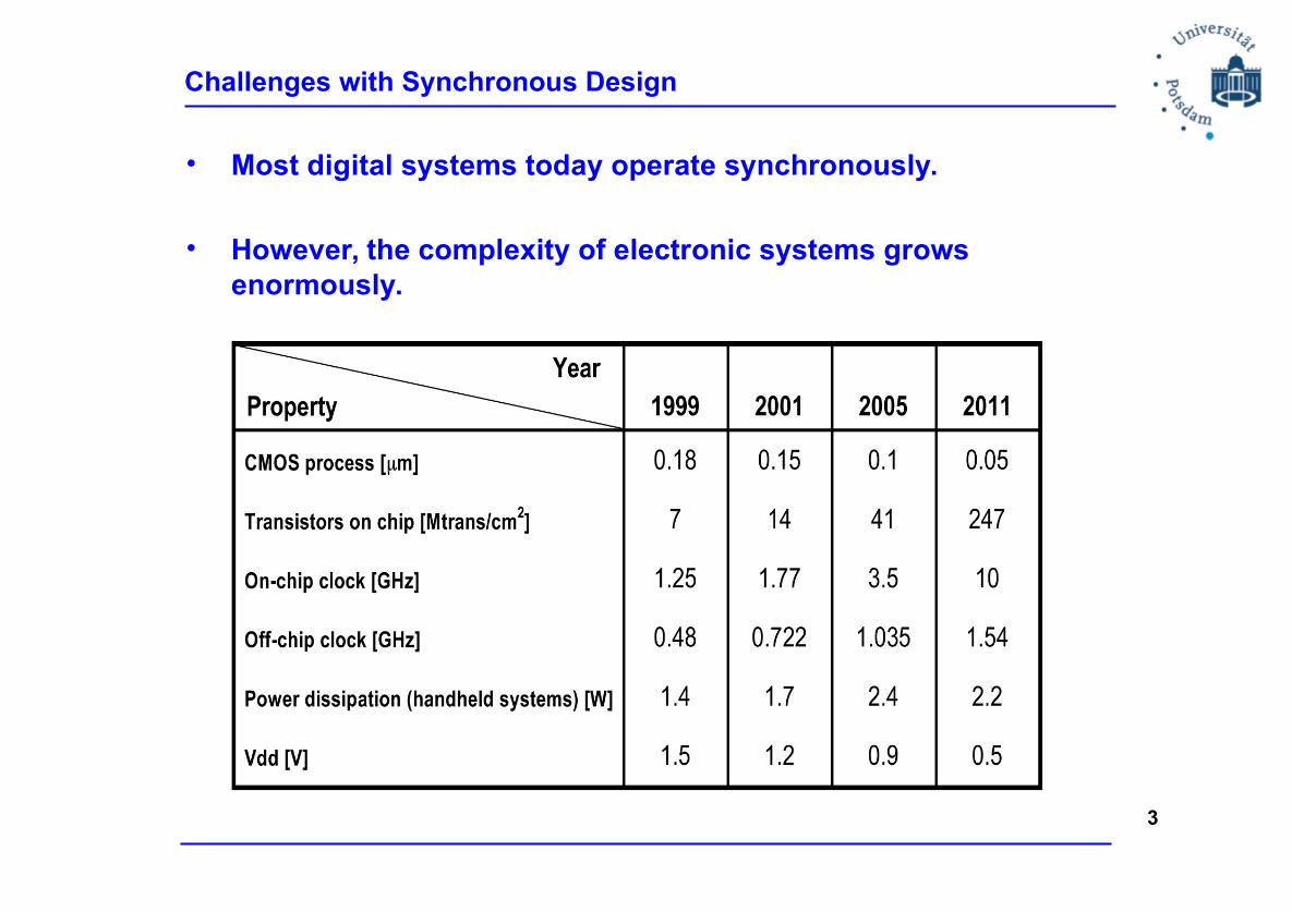
Challenges with Synchronous Design
• Most digital systems today operate synchronously.
• However, the complexity of electronic systems grows enormously.
3
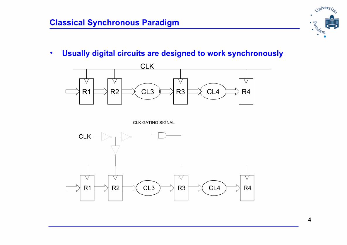
Classical Synchronous Paradigm
• Usually digital circuits are designed to work synchronously
R1 R2 R3CL3 R4CL4
CLK
CLK
CLK GATING SIGNAL
R1 R2 R3CL3 R4CL4
4
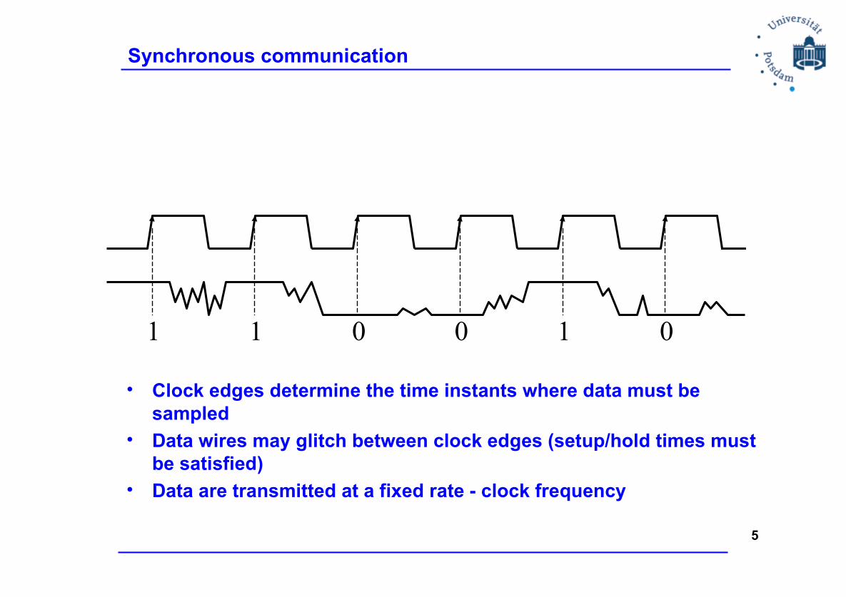
Synchronous communication
• Clock edges determine the time instants where data must be sampled
• Data wires may glitch between clock edges (setup/hold times must be satisfied)
• Data are transmitted at a fixed rate - clock frequency
1 1 0 0 1 0
5

Problems with Synchronous Design
• As clock speeds increase clock distribution becomes difficult:
We need to minimize clock skew.
There is some upper limit to clock speed that depends on the material properties of the device.
It is not possible to propagate a signal from one side of the chip to the other side within the single clock cycle
• Worst-case performance.
• Sensitive to variations in
Voltage, Temperature, Process.
• Not modular
(fixed clock rate: poor match for reusability of components).
• Clock burns large fraction of chip power (~40-70%)
• Synchronization failure.
6

What is Asynchronous Design ? (I)
• Synchronization is achieved without a global clock.
• Asynchronous Communication:
Handshake mechanisms
7
Sender Receiver
request
acknowledge
data
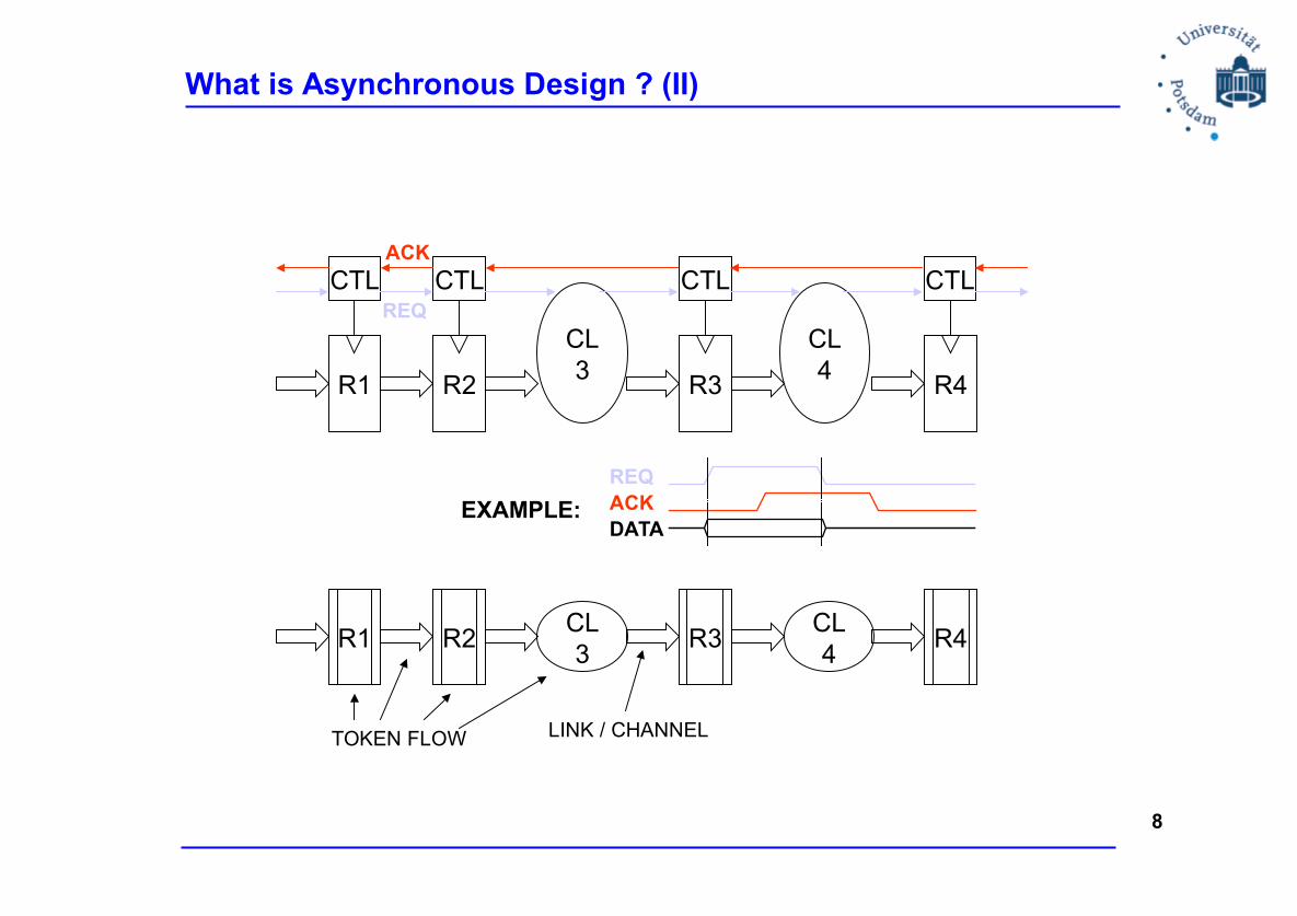
What is Asynchronous Design ? (II)
R1 R2 R3
CL3
R4
CTL CTL CTL CTL
CL4
REQ
ACK
R1 R2 R3CL3
R4CL4
LINK / CHANNELTOKEN FLOW
REQACKDATA
EXAMPLE:
8

9
A Behavioral Analogy
Asynchronous(local handshakebetween stages)
Synchronous(global CLK governs flow of data)
The chain of fire fighters:

Asynchronous design styles (I)
• Bundled data (Single Rail) 4 - phase protocol
This style is very widely used because of very small and fast asynchronous controllers
REQ
ACK
DATA
REQ
ACK
DATA
4 PHASE PROTOCOL:ALWAYS LIKE THIS
SOME VARIATIONS
n
10
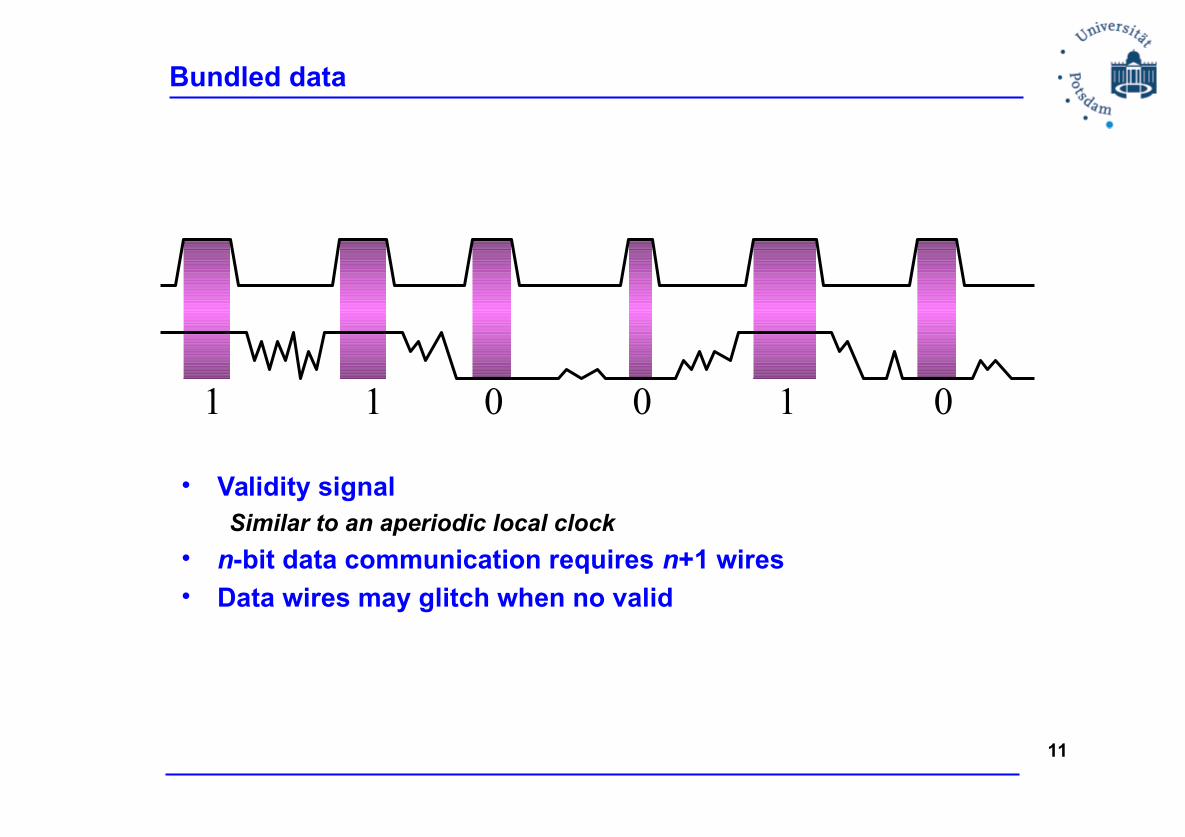
Bundled data
• Validity signalSimilar to an aperiodic local clock
• n-bit data communication requires n+1 wires• Data wires may glitch when no valid
1 1 0 0 1 0
11

Asynchronous design stiles (II)
• Bundled data (Single Rail) 2 - phase protocol
This style looks simpler and faster than 4-phase, but controllers are more complex
REQ
ACK
DATA
REQ
ACK
DATA
2 PHASE PROTOCOL
n
12

Asynchronous design stiles (III)
• 4-phase dual rail protocol
Each data bit encoded into 2 wires
Offers generation of Delay-Insensitive circuits
Introduces very big area overhead
ACK
DATA
ACK
DATA
2n
EMPTY 0 0VALUE d.t d.f
VALID “0” 0 1VALID “1” 1 0Not used 1 1
EMPTY EMPTY EMPTYVALID VALID VALID
E 10
13
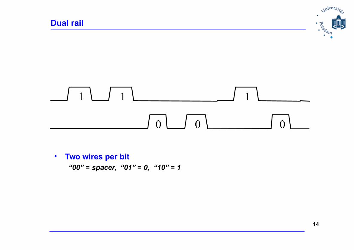
Dual rail
• Two wires per bit“00” = spacer, “01” = 0, “10” = 1
1 1
0 0
1
0
14

Asynchronous modules
• Signaling protocol:reqin+ start+ [computation] done+ reqout+ ackout+ ackin+reqin- start- [reset] done- reqout- ackout- ackin-
Data IN Data OUT
req in req out
ack in ack out
DATAPATH
CONTROL
start done
15
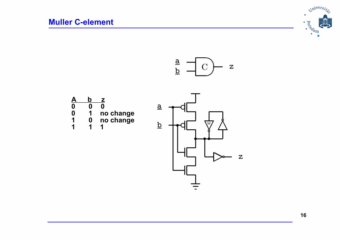
Muller C-element
0 0 0A b z
0 1 no change1 0 no change1 1 1
16
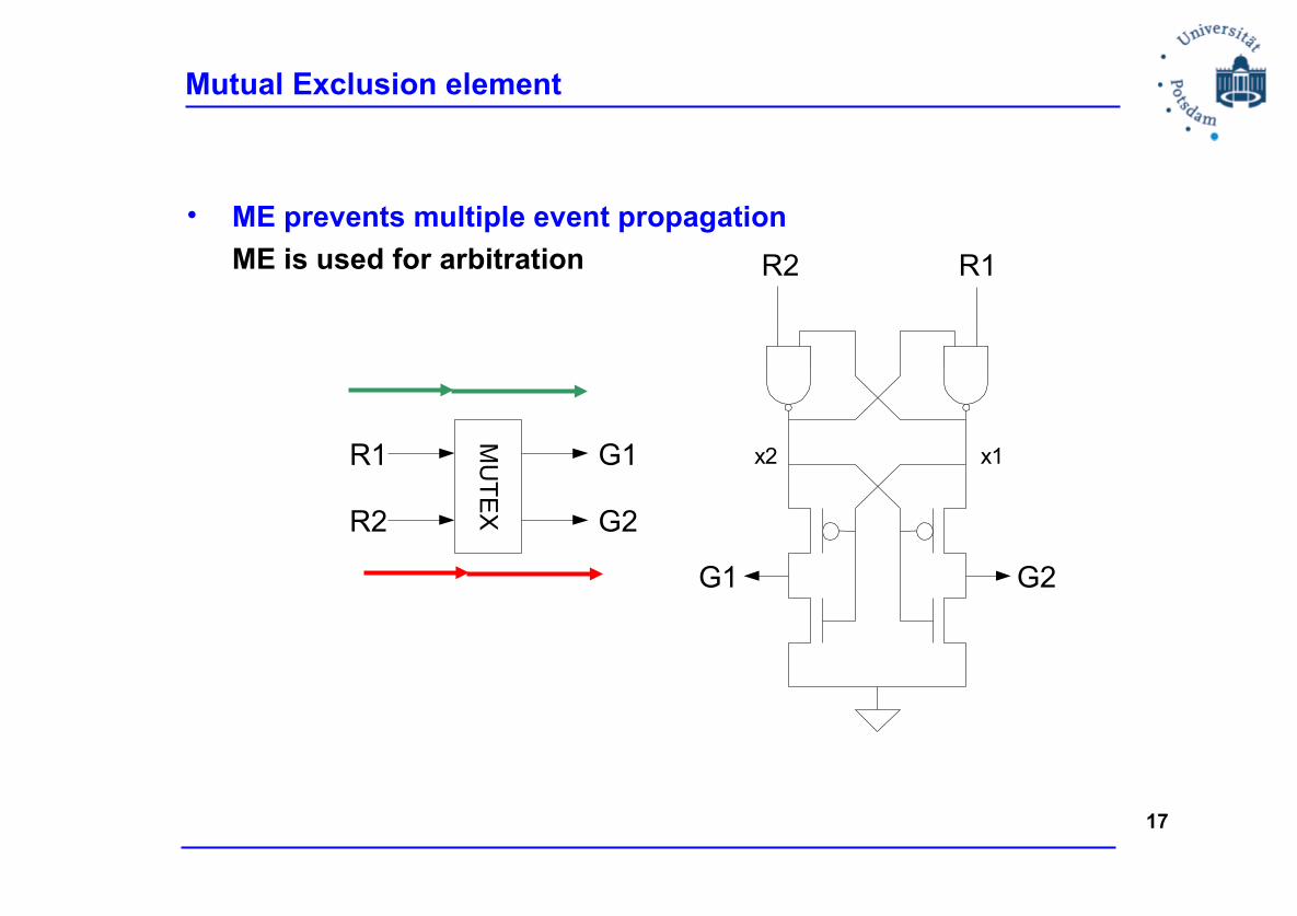
Mutual Exclusion element
• ME prevents multiple event propagation
ME is used for arbitration R1R2
G1 G2
MU
TE
X
R2
R1 G1
G2
x1x2
17
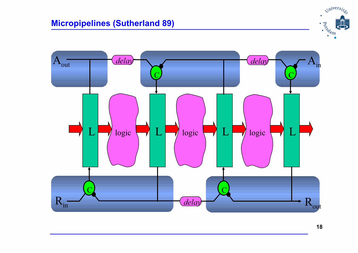
Micropipelines (Sutherland 89)
L L L Llogic logic logic
Rin
Aout
C C
C C
Rout
Aindelay
delay
delay
18

Abstract Pipeline
• Bubbles
• TokensValid (0 or 1, who cares) and Empty tokens
E V V E E
19
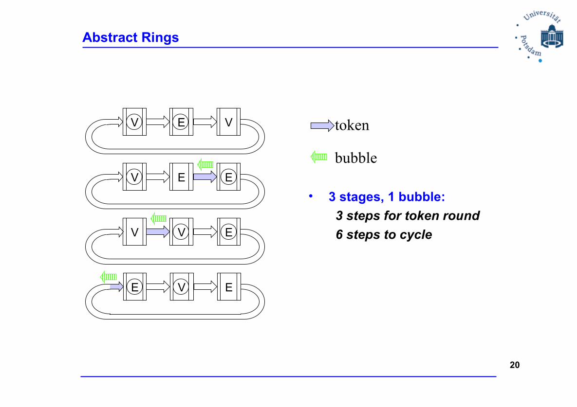
Abstract Rings
• 3 stages, 1 bubble:
3 steps for token round
6 steps to cycle
V E V
V E E
V V E
E V E
token
bubble
20
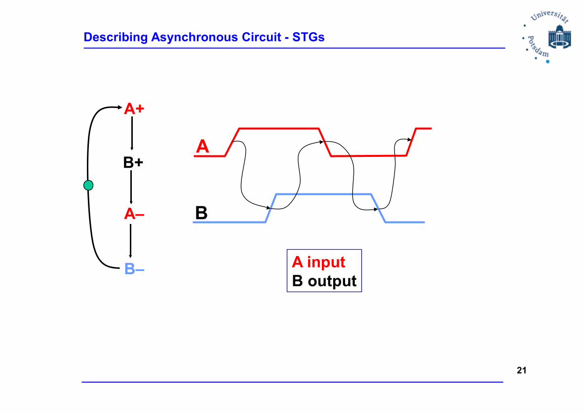
Describing Asynchronous Circuit - STGs
A+
B+
A–
B–
A
B
A inputB output
21
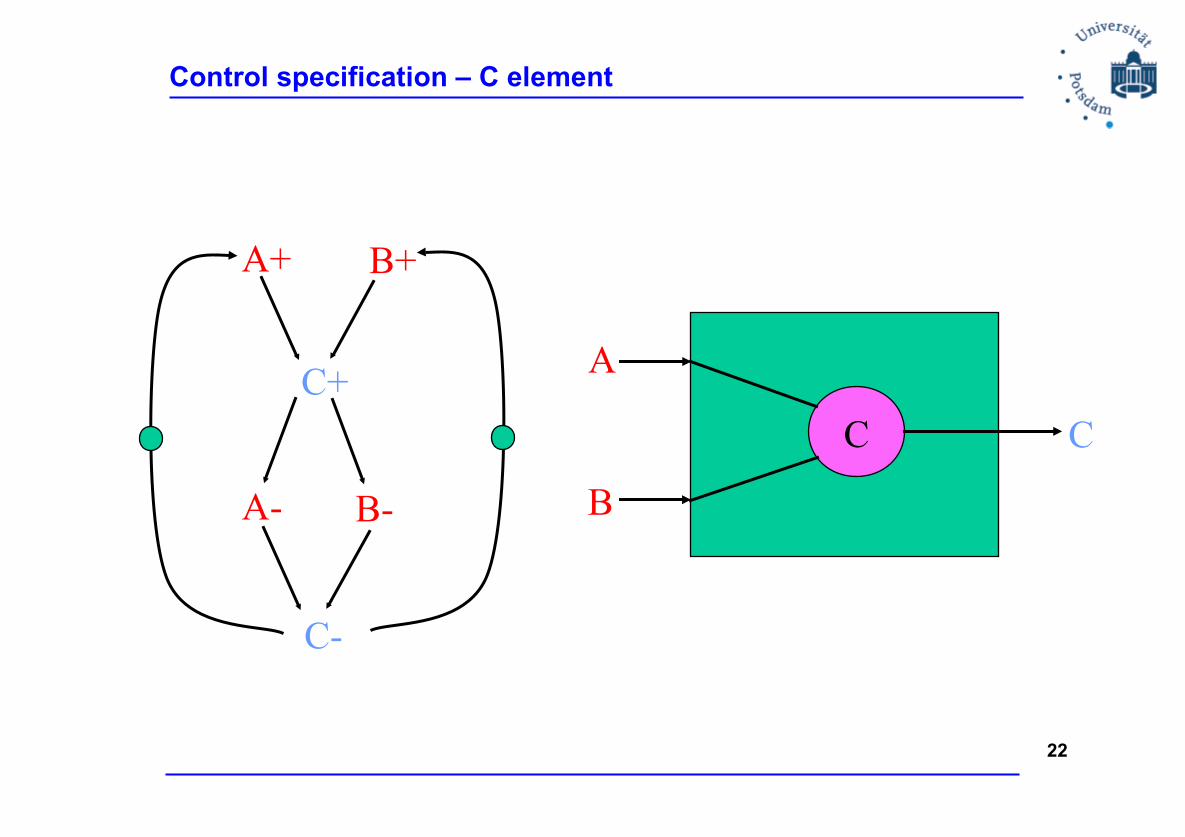
Control specification – C element
A+
C-
A-
C+A
C
B+
B- B
C
22
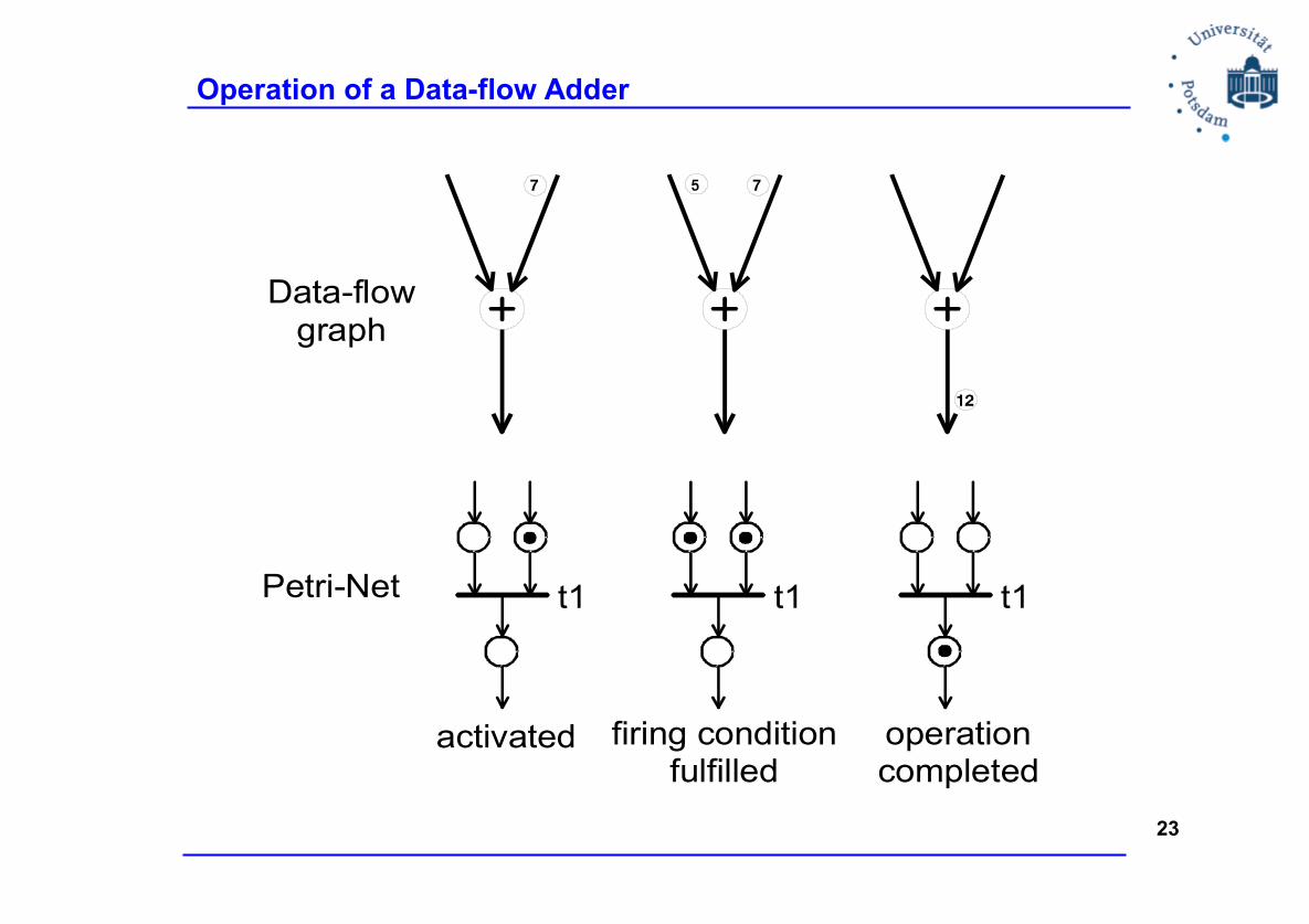
Operation of a Data-flow Adder
t1 t1 t1
activated firing conditionfulfilled
operationcompleted
Data-flowgraph
Petri-Net
23
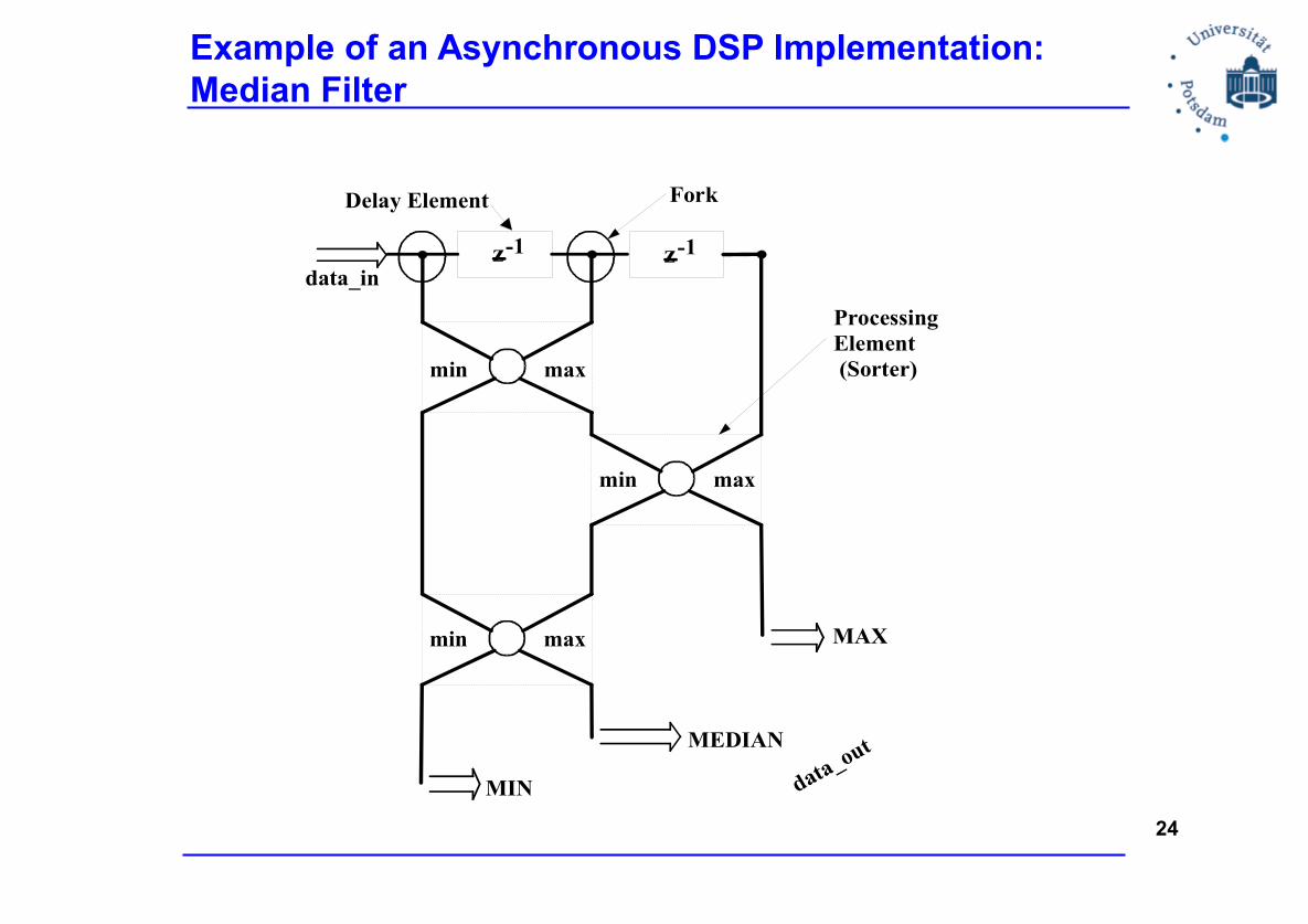
Example of an Asynchronous DSP Implementation: Median Filter
z-1 z-1
ProcessingElement (Sorter)min max
min max
min max
MIN
MEDIAN
MAX
data_in
ForkDelay Element
24
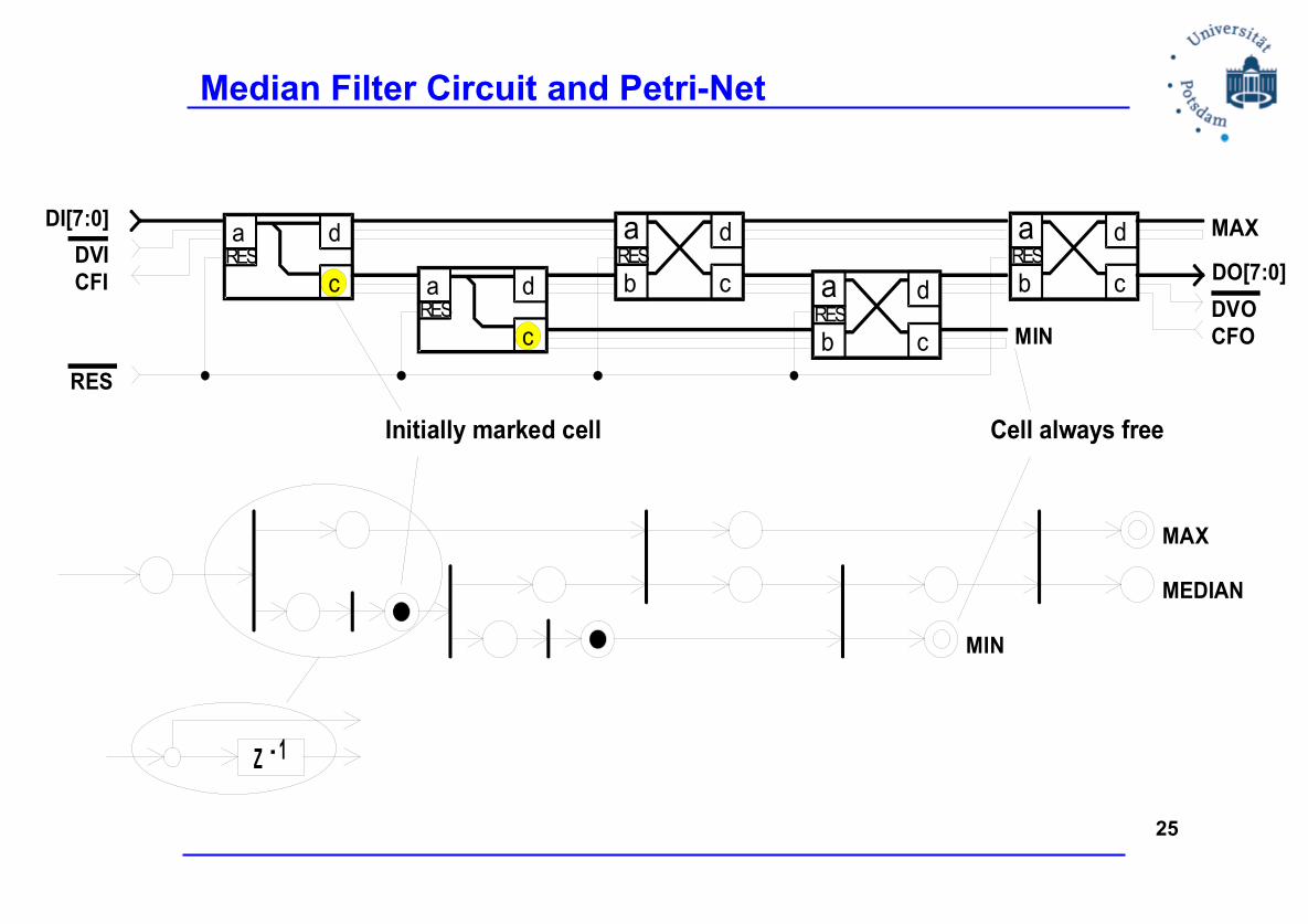
Median Filter Circuit and Petri-Net
DI[7:0]
DVICFI
DVOCFOMIN
MAX
RES
MAX
MIN
Z - 1
Initially marked cell Cell always free
MEDIAN
a
c
dRES
a
c
dRES
b DO[7:0]a
c
dRES
a
c
dRES
b
a
c
dRES
b
25
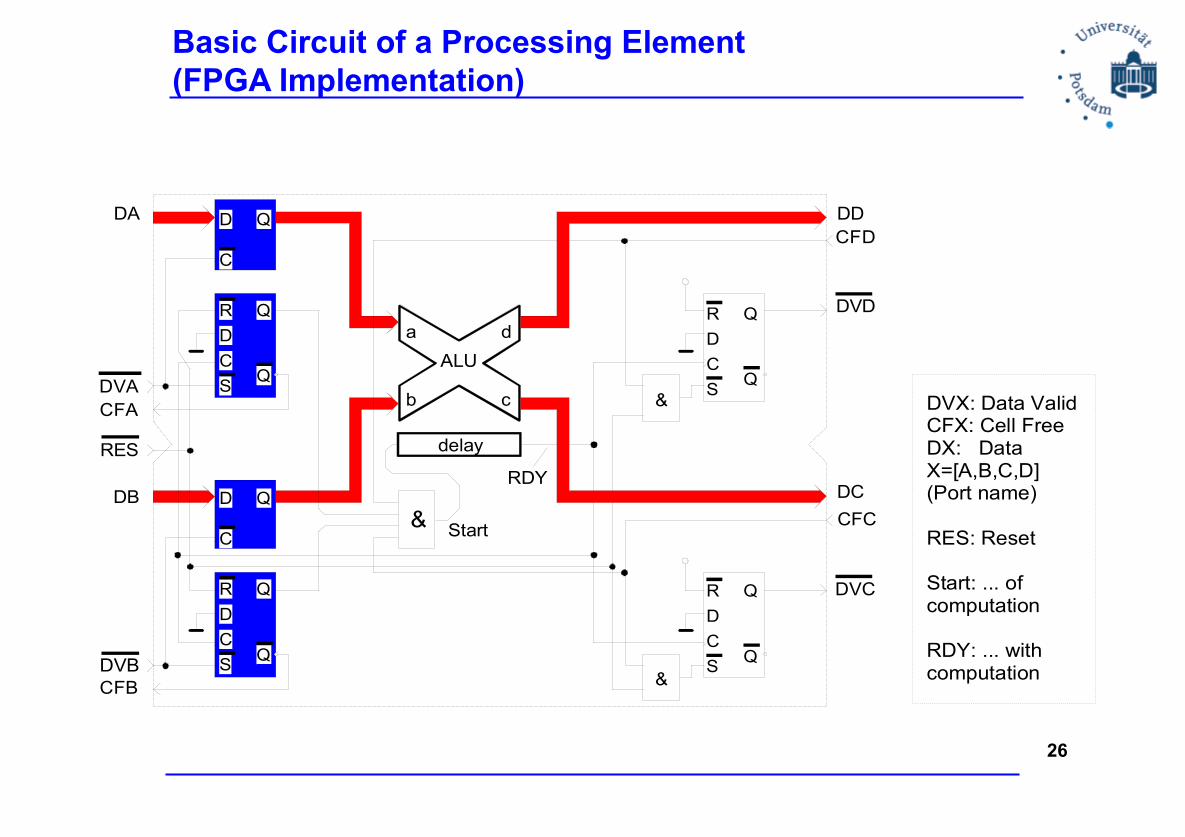
Basic Circuit of a Processing Element(FPGA Implementation)
a
b c
d
&
&
&
DVACFA
RES
DB
DA
DVBCFB
DDCFD
DVD
DC
CFC
DVC
DVX: Data ValidCFX: Cell FreeDX: DataX=[A,B,C,D](Port name)
RES: Reset
Start: ... of computation
RDY: ... withcomputation
delay
Start
RDY
ALU
Q
Q
Q
C
D
D
R
C
S
Q
Q
Q
C
D
D
R
C
S
Q
Q
D
R
C
S
Q
Q
D
R
C
S
26

Desynchronization - concept
• Start with synchronous design
• Replace clock with local handshake
• Use standard CAD tools
• Does not change datapath
• Guaranteed correctness
27
* Eyal Friedman, Desynchronization - From Synchronous to Asynchronous design, Seminar in VLSI Architecture, Technion, Israel, Spring 2008
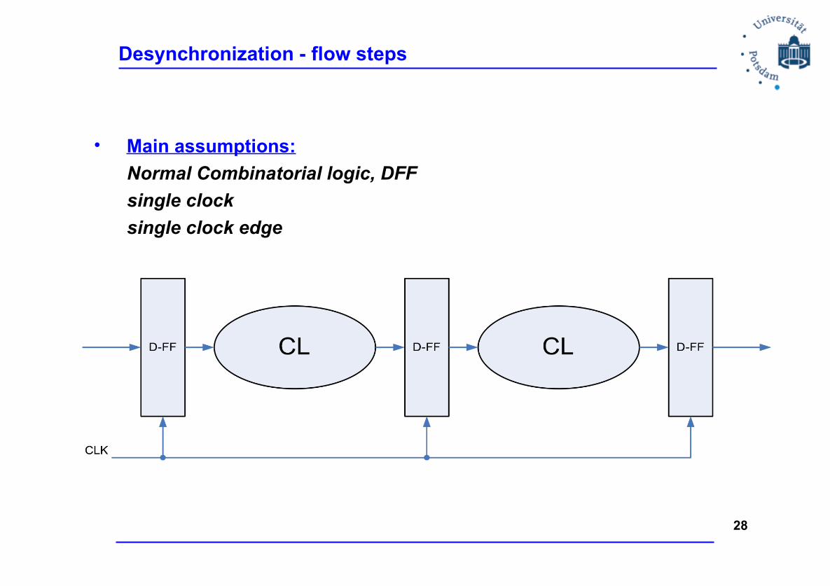
Desynchronization - flow steps
• Main assumptions:
Normal Combinatorial logic, DFF
single clock
single clock edge
28
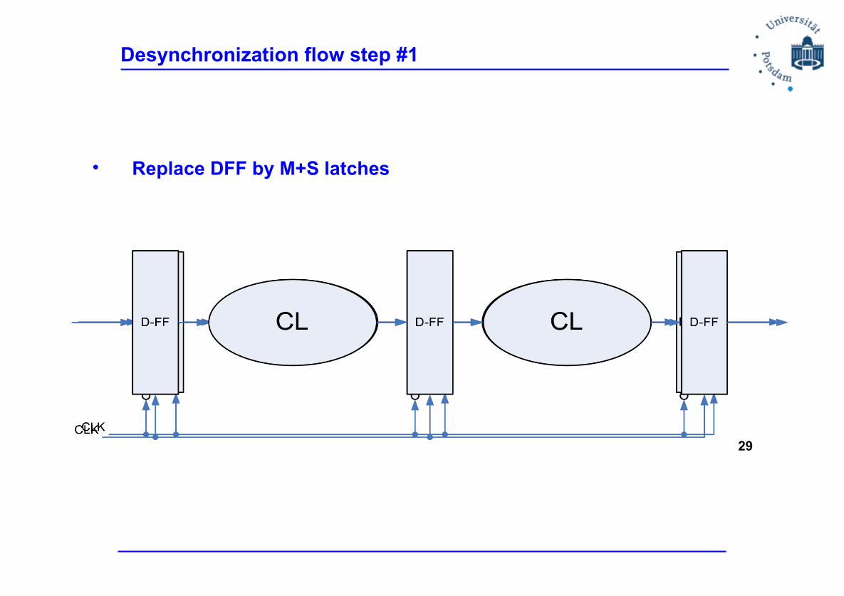
Desynchronization flow step #1
• Replace DFF by M+S latches
29

Desynchronization flow step #2
• Add matched delays
• Respect bundling assumption
Delay > Tpd of CL
Delay serves as completion signal
30

Desynchronization flow step #3
• Replace clock by local handshake controllers
31
Why Asynchronous Design?
• We are used to sync designLogic and timing assumptions are simpler, but not true in realityCurrently it is very hard to solve big problems of synchronous design like clock skew, big power consumption, process variability ...
• Common arguments for asynchronous design:Low power ? High speed ? Low emission ? Low sensitivity to PVT (Process, Voltage, Temperature) variations ? High modularity (SoC) ? No clock distribution and timing problems (works) ? Secure chips ?
32
Why not Asynchronous Design?
• Overhead (area, speed, power)
• Hard to designNon-decomposable to small combinatorial logic blocksConverting synchronous design to asynchronous typically fails
• Few CAD toolsThere is no real complete design-flow availableThere is only one commercial async EDA vendor available (Handshake Solutions) with very specific design flow (HASTE)
• Hard to testAsynchronous test methods are not present yet (or not mature enough), and it is difficult to go into any production without proper testing
33
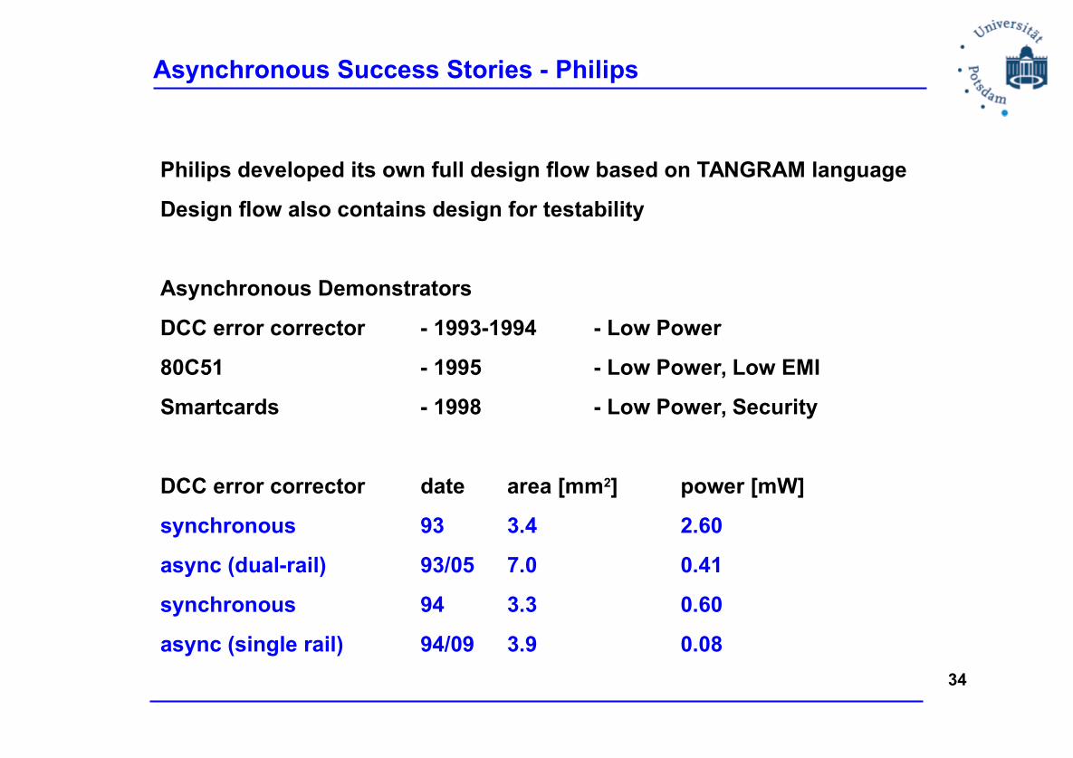
Asynchronous Success Stories - Philips
Philips developed its own full design flow based on TANGRAM language
Design flow also contains design for testability
Asynchronous Demonstrators
DCC error corrector - 1993-1994 - Low Power
80C51 - 1995 - Low Power, Low EMI
Smartcards - 1998 - Low Power, Security
DCC error corrector date area [mm2] power [mW]
synchronous 93 3.4 2.60
async (dual-rail) 93/05 7.0 0.41
synchronous 94 3.3 0.60
async (single rail) 94/09 3.9 0.08
34
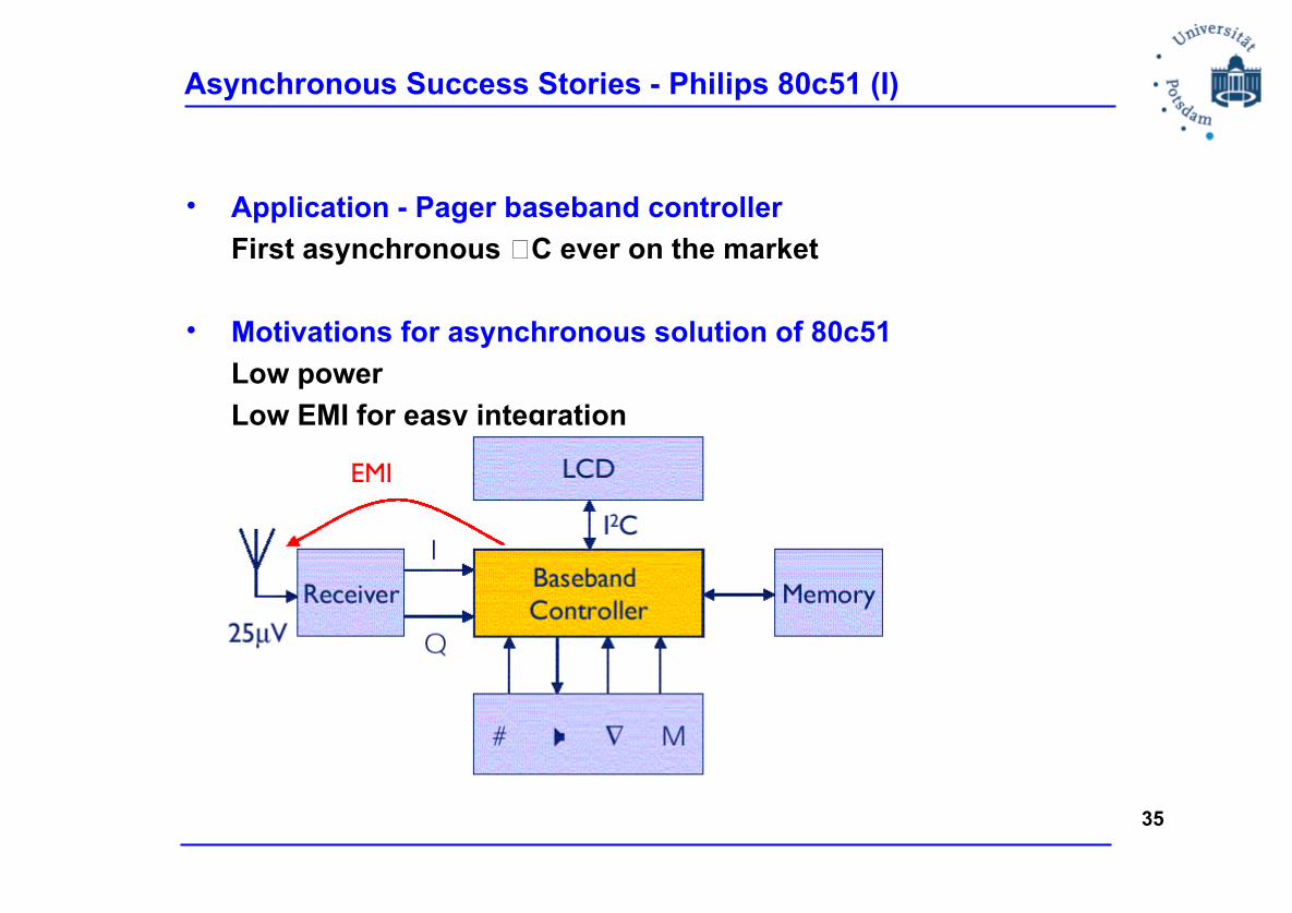
Asynchronous Success Stories - Philips 80c51 (I)
• Application - Pager baseband controller
First asynchronous C ever on the market
• Motivations for asynchronous solution of 80c51
Low power
Low EMI for easy integration
35
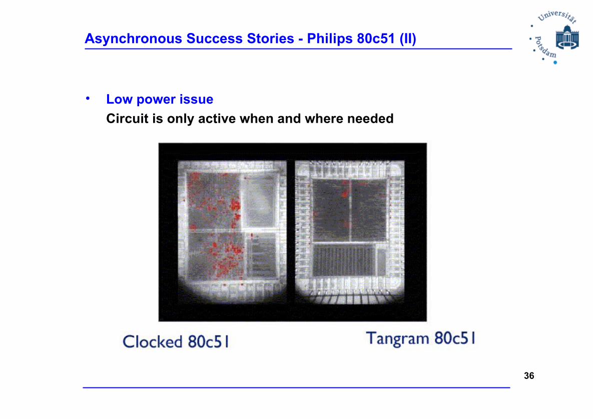
Asynchronous Success Stories - Philips 80c51 (II)
• Low power issue
Circuit is only active when and where needed
36
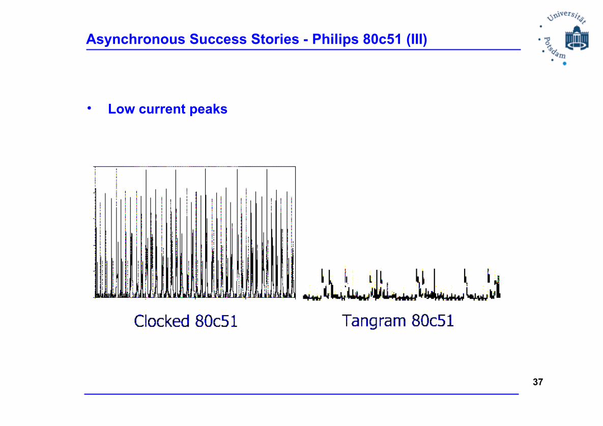
Asynchronous Success Stories - Philips 80c51 (III)
• Low current peaks
37
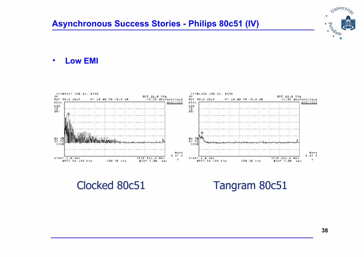
Asynchronous Success Stories - Philips 80c51 (IV)
• Low EMI
38
Asynchronous Success Stories - RAPPID
• RAPPID - Revolving Asynchronous Pentium Processor Instruction-length Decoder
• Instruction Length Decoder was performance bottleneck in ca. 1995-vintage CISC processors
• Potential for optimization for common cases (RISC-like)
• Results
Developed a novel aggressive asynchronous method
About 3x throughput T=3x
About one half latency L=2x
About one half power P=2x
About same area A=0.8x
Namely, this is TxLxPxA 10 improvement
39
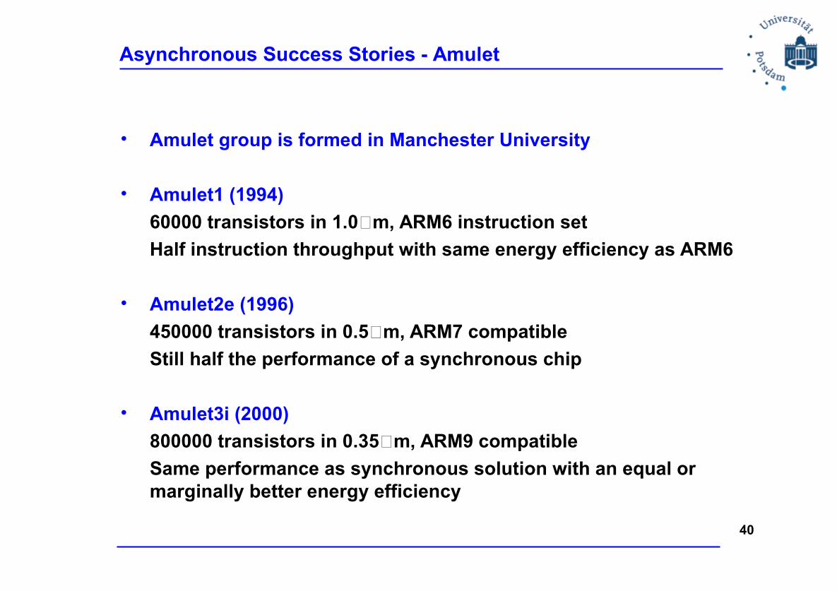
Asynchronous Success Stories - Amulet
• Amulet group is formed in Manchester University
• Amulet1 (1994)
60000 transistors in 1.0m, ARM6 instruction set
Half instruction throughput with same energy efficiency as ARM6
• Amulet2e (1996)
450000 transistors in 0.5m, ARM7 compatible
Still half the performance of a synchronous chip
• Amulet3i (2000)
800000 transistors in 0.35m, ARM9 compatible
Same performance as synchronous solution with an equal or marginally better energy efficiency
40

More recent activities – Fulcrum Microsystems
• Fulcrum is not Intel Switch and Router Division
• Fulcrum designs Ethernet switch silicon for data center network standards-based 10GbE and 40 Gigabit Ethernet (40GbE) switch silicon that have low latency and workload balancing capabilities
Half instruction throughput with same energy efficiency as ARM6
• Fulcrum designs are asynchronous
41
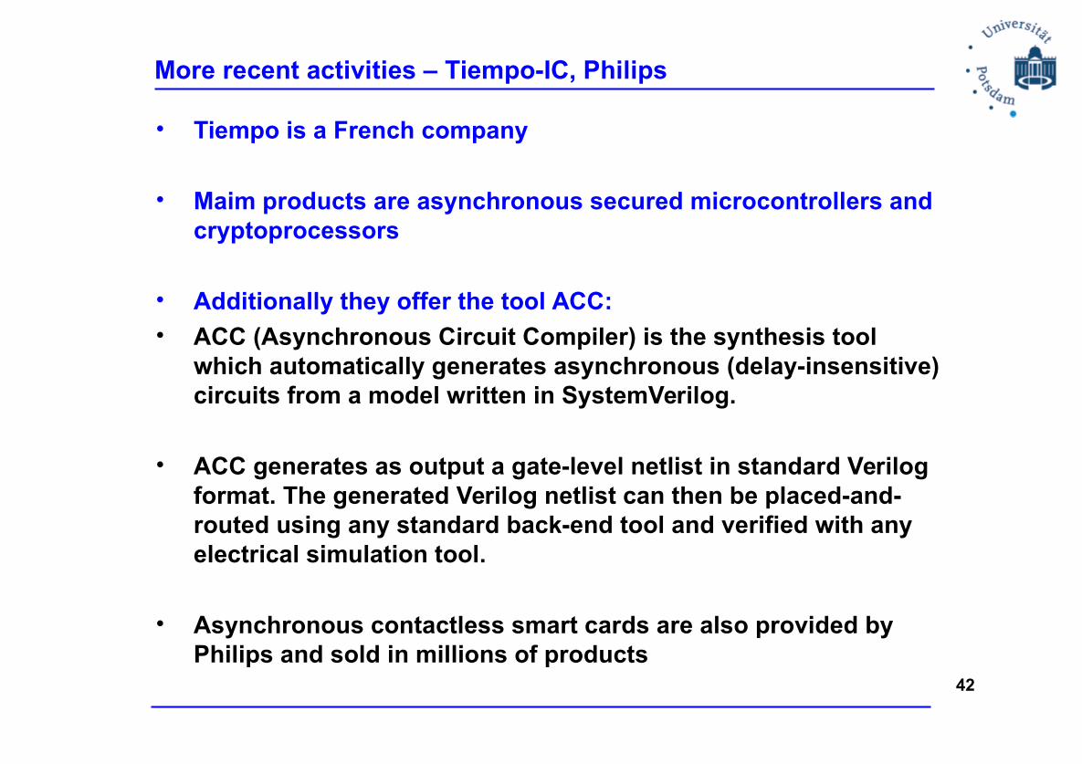
More recent activities – Tiempo-IC, Philips
• Tiempo is a French company
• Maim products are asynchronous secured microcontrollers and cryptoprocessors
• Additionally they offer the tool ACC:
• ACC (Asynchronous Circuit Compiler) is the synthesis tool which automatically generates asynchronous (delay-insensitive) circuits from a model written in SystemVerilog.
• ACC generates as output a gate-level netlist in standard Verilog format. The generated Verilog netlist can then be placed-and-routed using any standard back-end tool and verified with any electrical simulation tool.
• Asynchronous contactless smart cards are also provided by Philips and sold in millions of products
42

More recent activities – SpiNNaker
• SpiNNaker chip is a GALS system with 18 ARM968 processor nodes residing in synchronous islands, surrounded by packet-switched asynchronous communications infrastructure.
• The SpiNNaker engine is a massively-parallel multi-core computing system. It will contain up to 1,036,800 ARM9 cores and 7Tbytes of RAM distributed throughout the system in 57K nodes, each node being a System-in-Package (SiP) containing 18 cores plus a 128Mbyte off-die SDRAM (Synchronous Dynamic Random Access Memory)
• This will correspond to 1% of human brain capacity
43

Globally Asynchronous Locally Synchronous (GALS) Systems
44
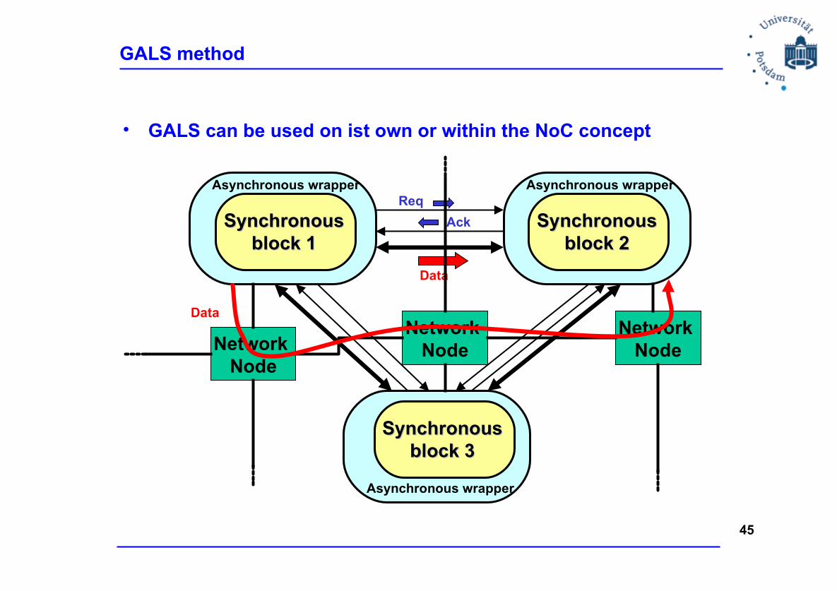
Asynchronous wrapper
GALS method
Req
Ack
Data
SynchronousSynchronousblock 3block 3
SynchronousSynchronousblock 1block 1
SynchronousSynchronousblock 2block 2
Asynchronous wrapper
Asynchronous wrapper
Network Node
Network Node
Network Node
Data
• GALS can be used on ist own or within the NoC concept
45

GALS as a Powerful Design Technique
• In the wireless communication systems GALS can approach the main design challenges.
• GALS makes data transfer between the blocks very easy.
• Design problems as timing closure or clock-tree generation are limited to the level of much smaller local blocks.
• Decoupling of local blocks from central clock source reduces spectral noise considerably.
• Power saving is automatically integrated in asynchronous wrapper.
46
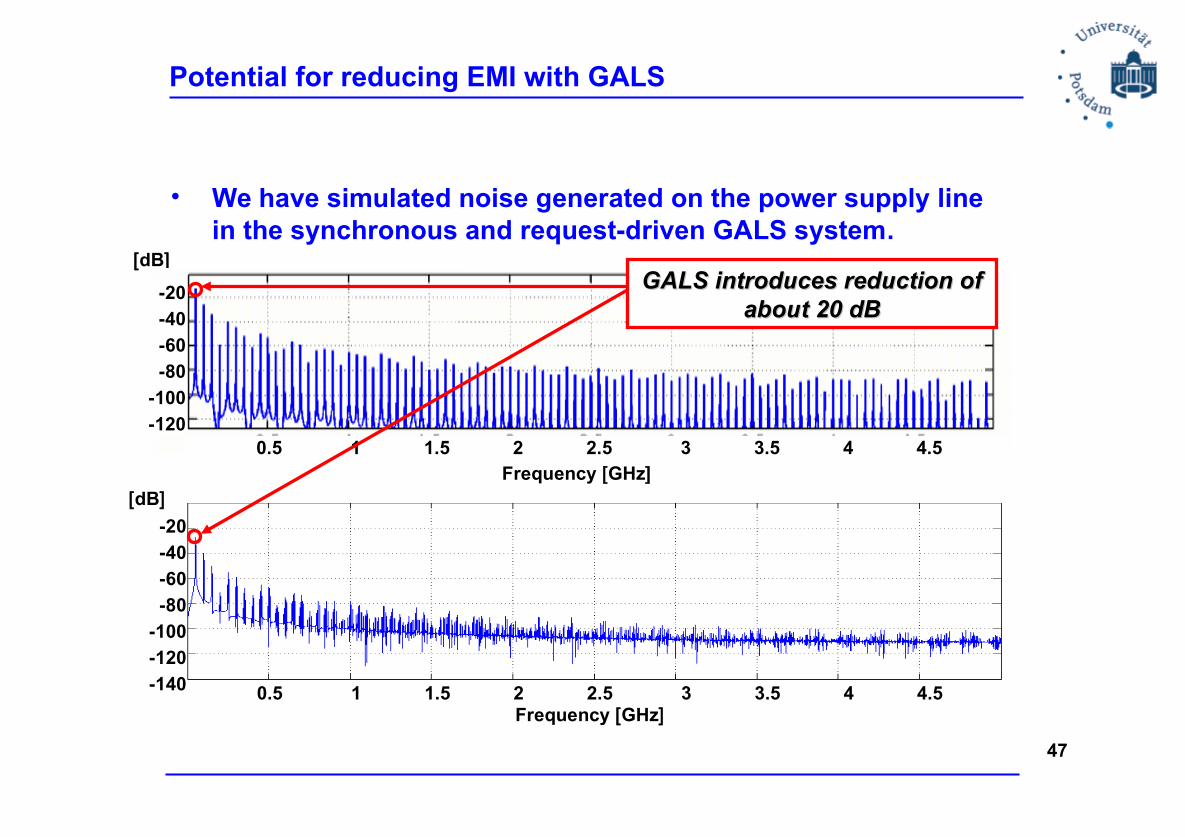
Potential for reducing EMI with GALS
• We have simulated noise generated on the power supply line in the synchronous and request-driven GALS system.
[dB]
Frequency [GHz]
Frequency [GHz]
47
0.5 1 1.5 2 2.5 3 3.5 4 4.5
-20
-40
-60
-80
-100
-120
0.5 1 1.5 2 2.5 3 3.5 4 4.5
-20
-40
-60
-80
-100
-120
-140
[dB]
GALS introduces reduction of GALS introduces reduction of about 20 dBabout 20 dB
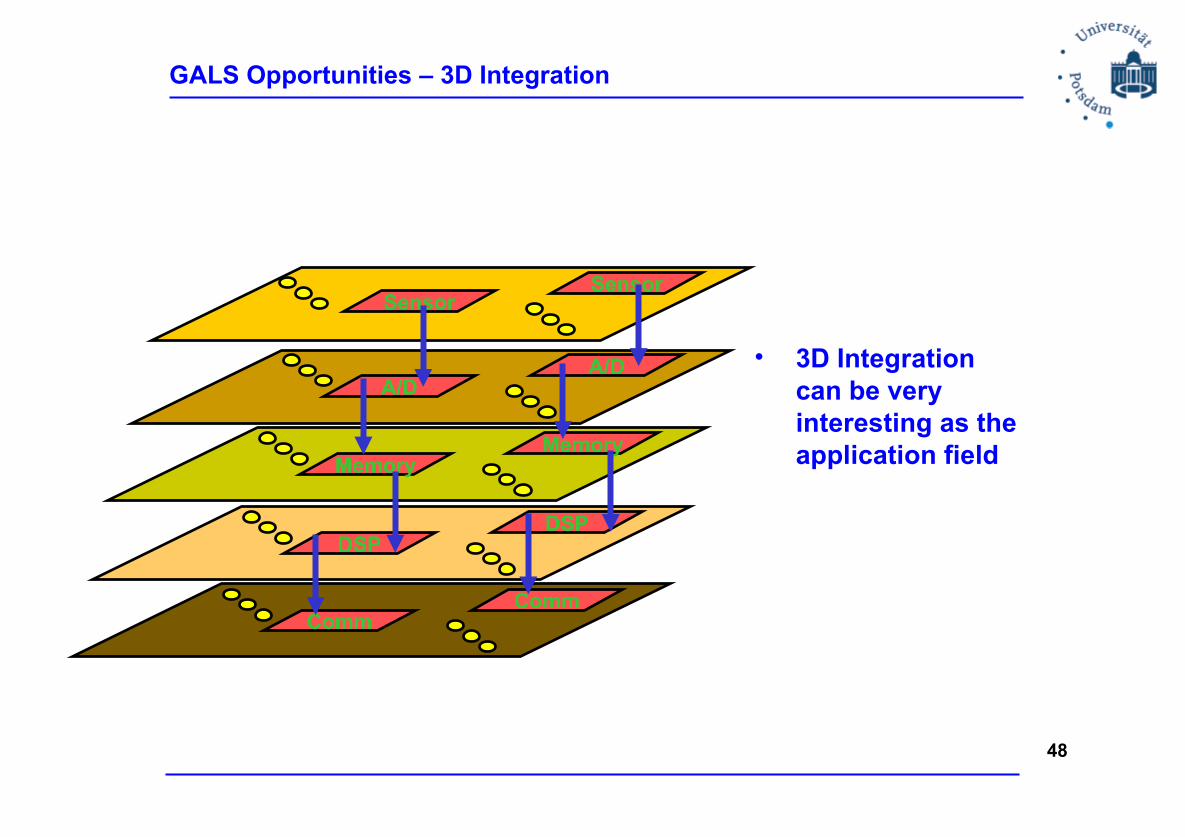
GALS Opportunities – 3D Integration
• 3D Integration can be very interesting as the application field
SensorSensor
A/DA/D
MemoryMemory
DSPDSP
CommComm
48
GALS Opportunities – Process Scaling and Variability
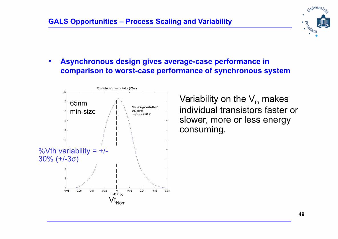
• Asynchronous design gives average-case performance in comparison to worst-case performance of synchronous system
Variability on the Vth makes individual transistors faster or slower, more or less energy consuming.
65nmmin-size
VtNom
%Vth variability = +/- 30% (+/-3σ)
49

GALS Methods
• GALS based on synchronizers
• GALS based on asynchronous FIFOs
• GALS based on pausible clocking
50
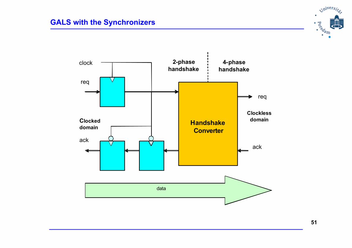
GALS with the Synchronizers
req
ack
req
ack
Handshake Converter
2-phase handshake
4-phase handshake
data
Clockless domain
Clocked domain
clock
51

GALS with FIFOs
52
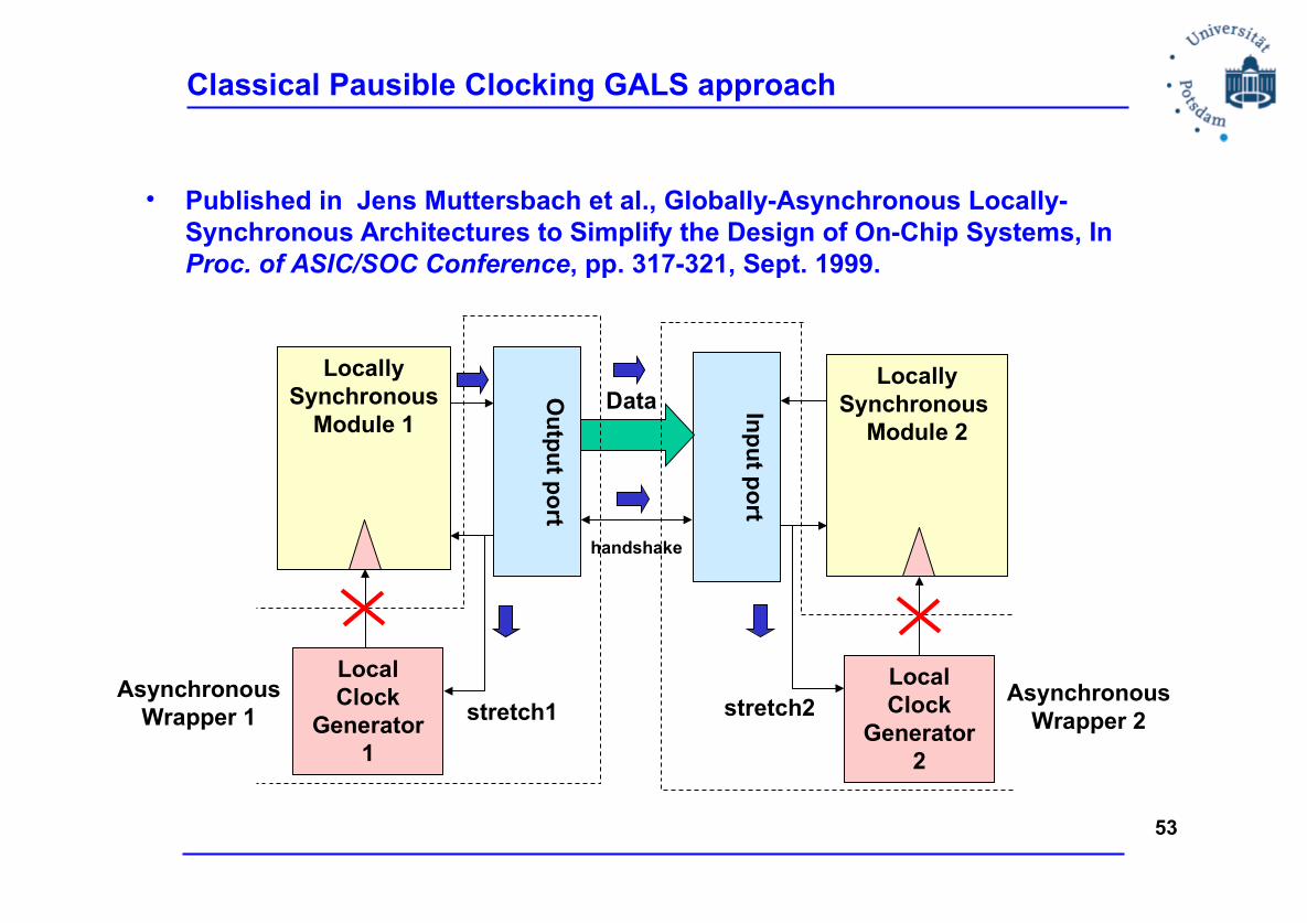
Classical Pausible Clocking GALS approach
Locally Synchronous
Module 1
Local Clock
Generator1
Ou
tpu
t po
rt
Locally Synchronous
Module 2
Local Clock
Generator2
Inp
ut p
ort
Data
stretch1 stretch2
• Published in Jens Muttersbach et al., Globally-Asynchronous Locally-Synchronous Architectures to Simplify the Design of On-Chip Systems, In Proc. of ASIC/SOC Conference, pp. 317-321, Sept. 1999.
53
Asynchronous Wrapper 1
Asynchronous Wrapper 2
handshake
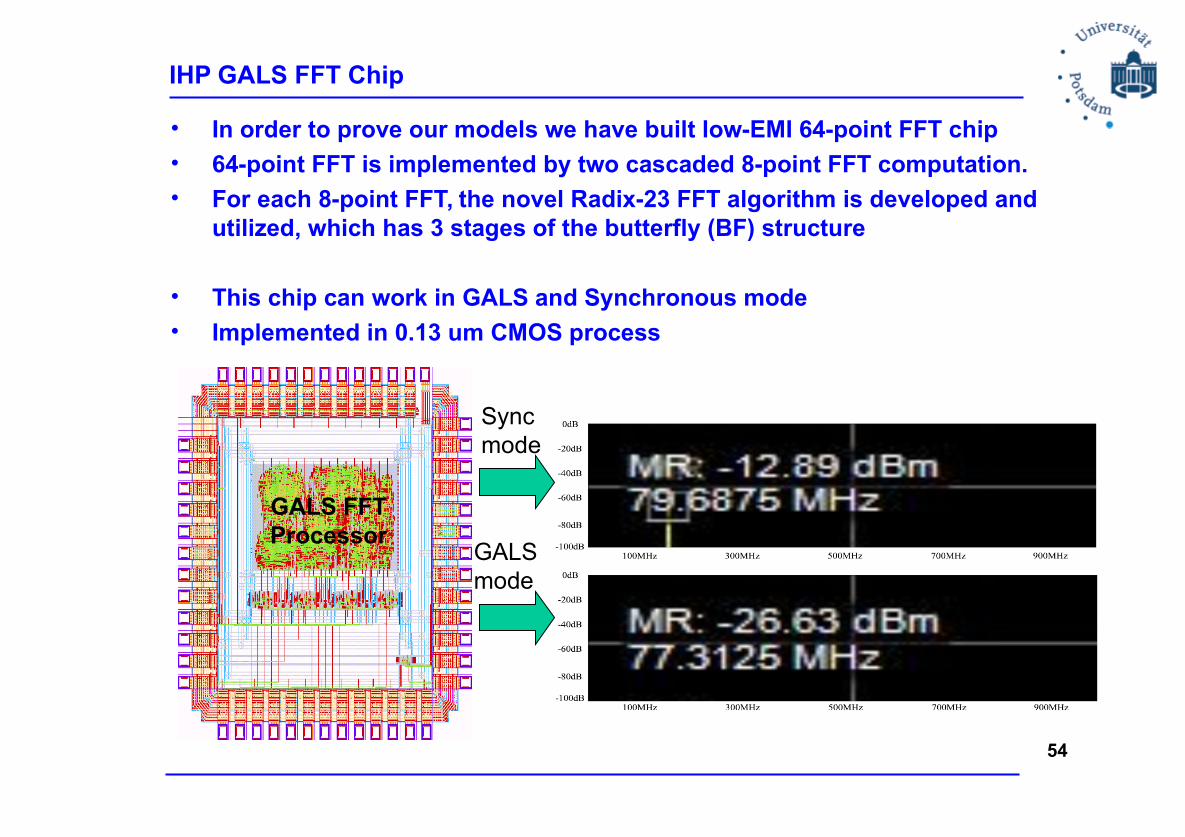
IHP GALS FFT Chip
• In order to prove our models we have built low-EMI 64-point FFT chip
• 64-point FFT is implemented by two cascaded 8-point FFT computation.
• For each 8-point FFT, the novel Radix-23 FFT algorithm is developed and utilized, which has 3 stages of the butterfly (BF) structure
• This chip can work in GALS and Synchronous mode
• Implemented in 0.13 um CMOS process
GALS FFT Processor
Sync mode
GALS mode
54
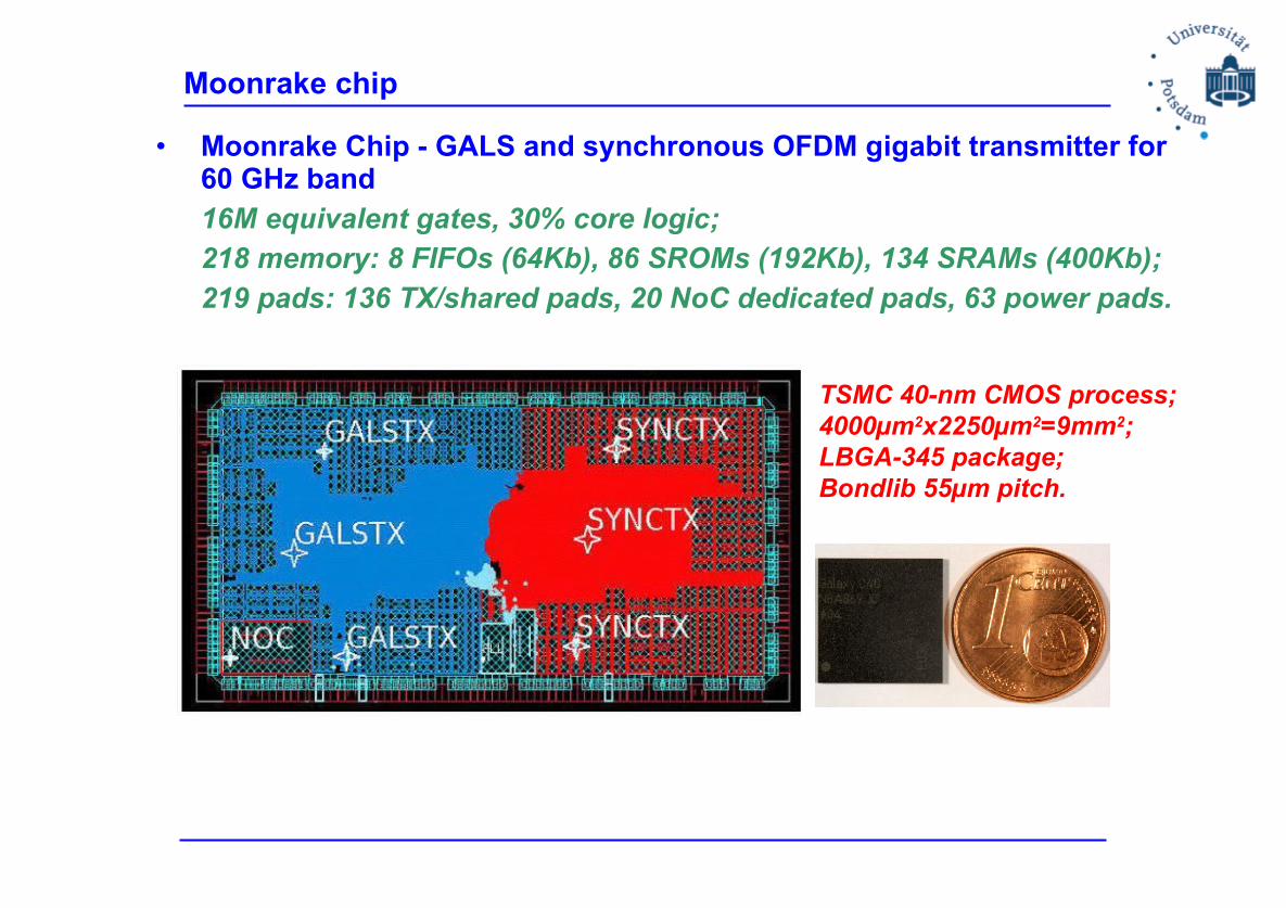
Moonrake chip
• Moonrake Chip - GALS and synchronous OFDM gigabit transmitter for 60 GHz band16M equivalent gates, 30% core logic;218 memory: 8 FIFOs (64Kb), 86 SROMs (192Kb), 134 SRAMs (400Kb);219 pads: 136 TX/shared pads, 20 NoC dedicated pads, 63 power pads.
TSMC 40-nm CMOS process;4000µm2x2250µm2=9mm2;LBGA-345 package;Bondlib 55µm pitch.
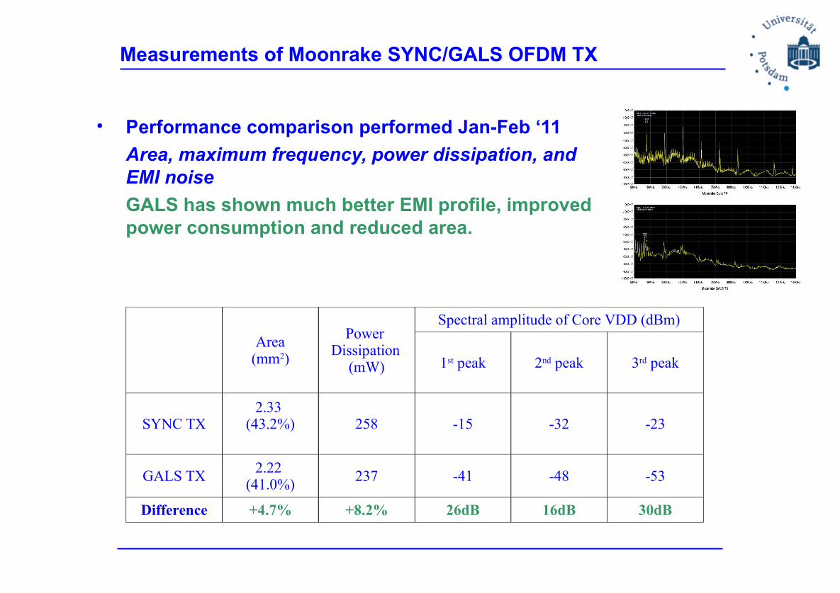
Measurements of Moonrake SYNC/GALS OFDM TX
• Performance comparison performed Jan-Feb ‘11
Area, maximum frequency, power dissipation, and EMI noise
GALS has shown much better EMI profile, improved power consumption and reduced area.
Area(mm2)
Power Dissipation
(mW)
Spectral amplitude of Core VDD (dBm)
1st peak 2nd peak 3rd peak
SYNC TX2.33
(43.2%) 258 -15 -32 -23
GALS TX2.22
(41.0%)237 -41 -48 -53
Difference +4.7% +8.2% 26dB 16dB 30dB
Synchronous and GALS Networks on Chips
57
Synchronous and GALS NoCs
• Today on-chip design is more and more communication-centric
• Classical topologies are not sufficient (point-to-point, mesh, bus, etc.)
• Shared bus = low performance Bandwidth is shared
Bus width (bits) relatively small
Global clock frequency limited
• Disadvantage of multiple busesNot scalable, not generic
• Promising alternative could be Networks on Chip (NoCs)
• NoCs can be implemented completely synchronously, mesochronously, or in GALS fashion
58

Bus vs. Network Arguments
BUS NoC
Scalability: Every IP adds parasitic capacitance
Only P2P connections
Timing is difficult Can be pipelined
Bus Arbiter performance Load shared by routers
Bandwidth: Limited and shared by all IP
Scales with network size
Latency: Zero when granted control Network latency always exists
Cost: Low area Significant area
Design Complexity:
Simple: well known and understood
Requires changes in HW and sometimes SW levels
59
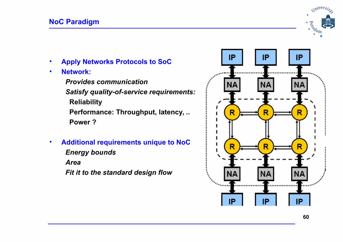
NoC Paradigm
• Apply Networks Protocols to SoC
• Network:
Provides communication
Satisfy quality-of-service requirements:
Reliability
Performance: Throughput, latency, ..
Power ?
• Additional requirements unique to NoC
Energy bounds
Area
Fit it to the standard design flow
60
Switching Network Basics
• Transport Layer: Msg end-to-end
Implemented using network adapters
Assembly and disassembly of the packets at source/destination
• Network Layer: Pkt end-to-end
Implemented using routers
Routers decide the routing path to destination
header of the packet
topology knowledge
Scalable distributed system: load shared between routers
• Data-Link Layer : Pkt over link
Packets: header, payload, trailer
Error correction (on packet): redundancy, error correction codes
* Technion - Asynchronous NoC - Nikolai Samolazov
61
Limitations of Fully-Synchronous Networks
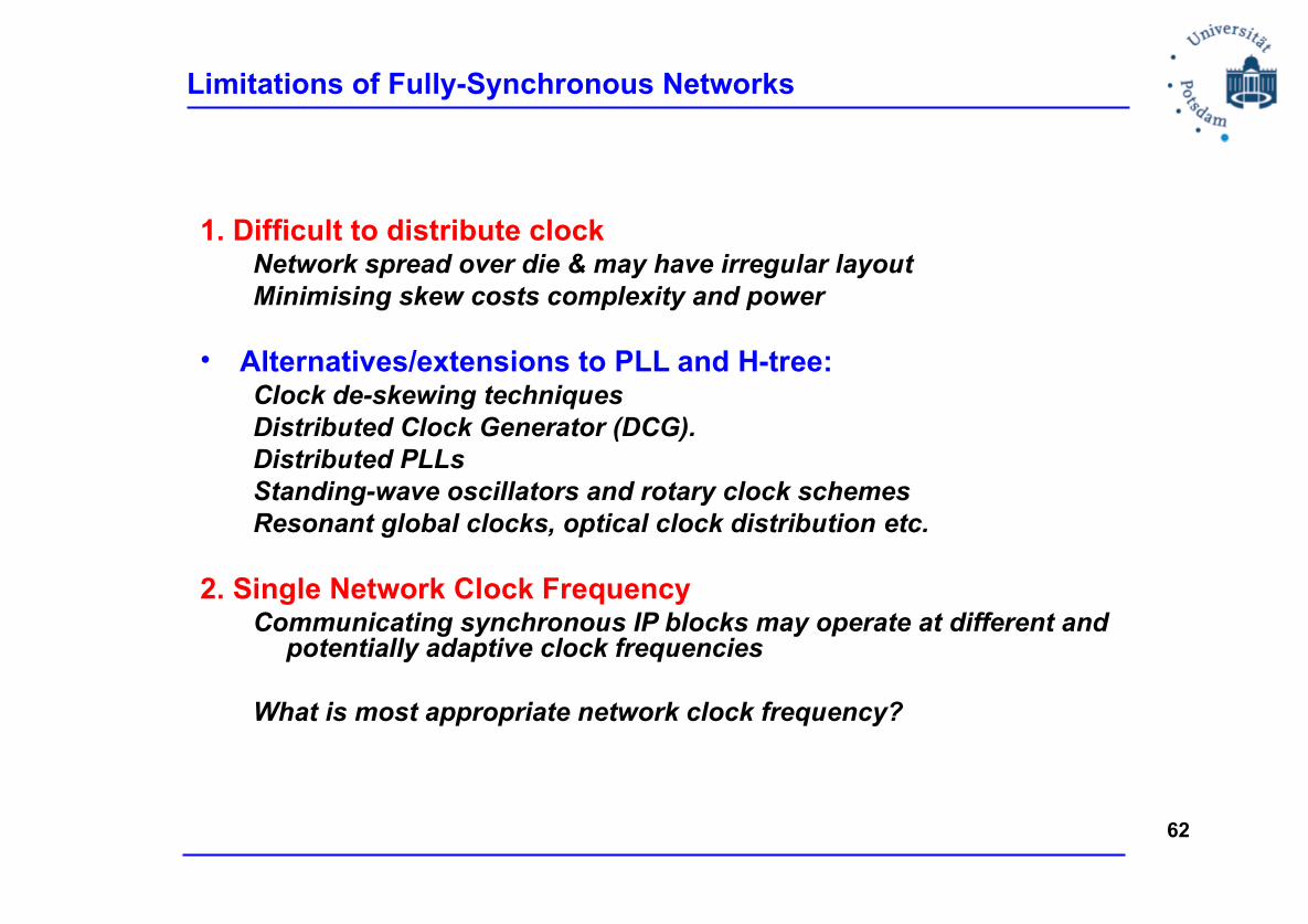
1. Difficult to distribute clock Network spread over die & may have irregular layoutMinimising skew costs complexity and power
• Alternatives/extensions to PLL and H-tree:Clock de-skewing techniquesDistributed Clock Generator (DCG). Distributed PLLsStanding-wave oscillators and rotary clock schemesResonant global clocks, optical clock distribution etc.
2. Single Network Clock FrequencyCommunicating synchronous IP blocks may operate at different and
potentially adaptive clock frequencies
What is most appropriate network clock frequency?
62
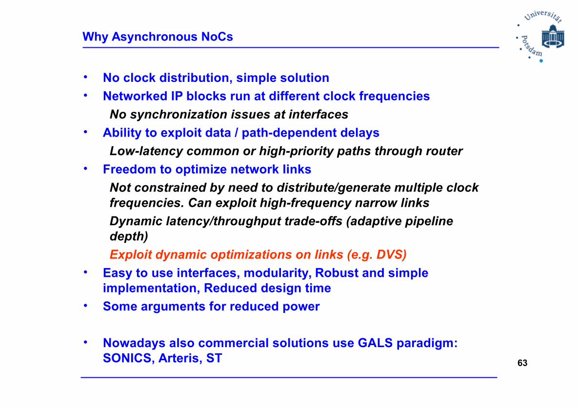
Why Asynchronous NoCs
• No clock distribution, simple solution
• Networked IP blocks run at different clock frequencies
No synchronization issues at interfaces
• Ability to exploit data / path-dependent delays
Low-latency common or high-priority paths through router
• Freedom to optimize network links
Not constrained by need to distribute/generate multiple clock frequencies. Can exploit high-frequency narrow links
Dynamic latency/throughput trade-offs (adaptive pipeline depth)
Exploit dynamic optimizations on links (e.g. DVS)
• Easy to use interfaces, modularity, Robust and simple implementation, Reduced design time
• Some arguments for reduced power
• Nowadays also commercial solutions use GALS paradigm: SONICS, Arteris, ST 63
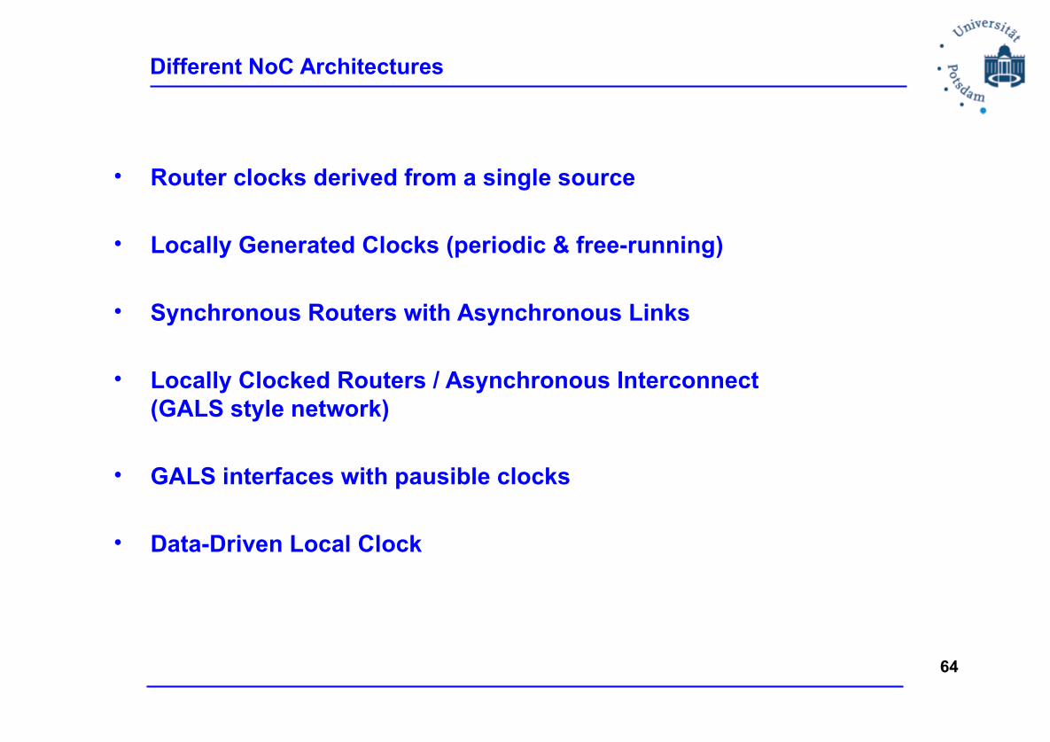
Different NoC Architectures
• Router clocks derived from a single source
• Locally Generated Clocks (periodic & free-running)
• Synchronous Routers with Asynchronous Links
• Locally Clocked Routers / Asynchronous Interconnect (GALS style network)
• GALS interfaces with pausible clocks
• Data-Driven Local Clock
64
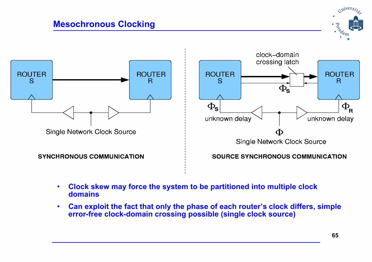
Mesochronous Clocking
• Clock skew may force the system to be partitioned into multiple clock domains
• Can exploit the fact that only the phase of each router’s clock differs, simple error-free clock-domain crossing possible (single clock source)
65

Using Synchronisers for GALS NoCs
• Asynchronous channel uses 4-phase bundled data protocol
A. Sheibanyrad, A. Greiner, Two efficient synchronous asynchronous converters well-suited for networks-on-chip in GALS architectures, 2005
66
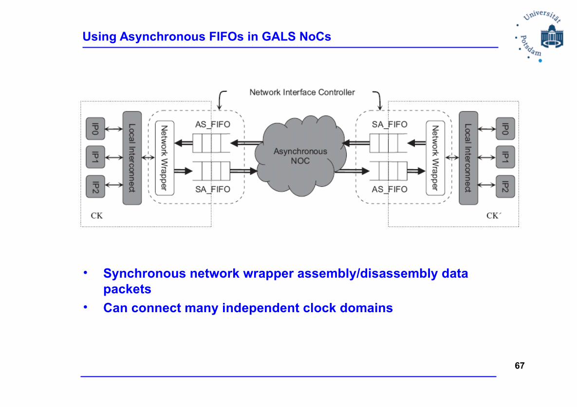
Using Asynchronous FIFOs in GALS NoCs
• Synchronous network wrapper assembly/disassembly data packets
• Can connect many independent clock domains
67

NoC architecture for DVFS – LETI Solution (NoCs 2008)
• A fully asynchronous Network-on-Chip
• IP units are synchronous islands using programmable Local Clock Generator
• Within the IP unit
Synchronization is done thanks to Pausable Clock
A Power Unit manages internal Vcore generated using external Vhigh and Vlow
A Network Interface is in charge of
NoC communications
Local Power Management• A local fine grain Dynamic Voltage Scaling
• A local fine grain Dynamic Frequency Scaling
68
Conclusions
• Asynchronous design style is an alternative to classical synchronous approach
• Potentially it offers better system integration features, reduced EMI, and with some luck better power profile with small performance/area penalty
• Design and test flow remains as a problem of this design style
• One compromise is GALS approach that can be used for system integration of complex SoCs
• This method is especially attractive for NoC designs
69