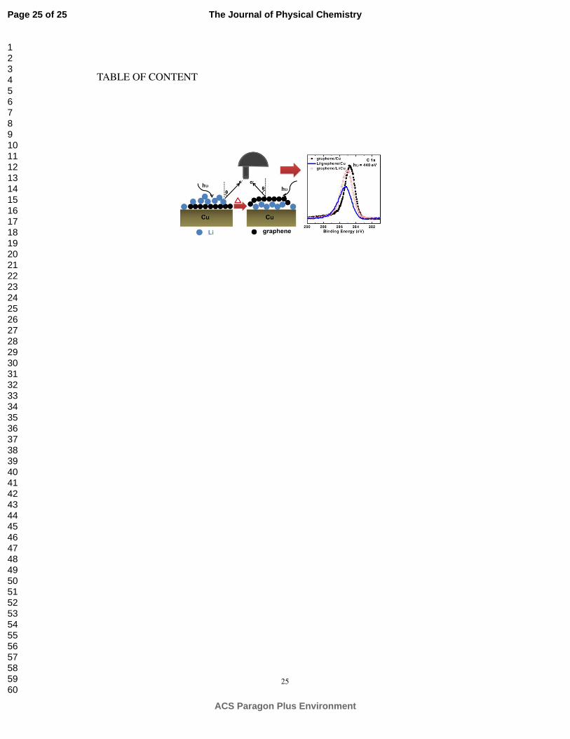
intercalation of li at the graphene/cu interface
TRANSCRIPT
Subscriber access provided by UNIV ILLINOIS URBANA
The Journal of Physical Chemistry C is published by the American Chemical Society.1155 Sixteenth Street N.W., Washington, DC 20036Published by American Chemical Society. Copyright © American Chemical Society.However, no copyright claim is made to original U.S. Government works, or worksproduced by employees of any Commonwealth realm Crown government in the courseof their duties.
Article
Intercalation of Li at the Graphene/Cu InterfaceLiang Zhang, Yifan Ye, Dingling Cheng, Haibin Pan, and Junfa Zhu
J. Phys. Chem. C, Just Accepted Manuscript • DOI: 10.1021/jp401290f • Publication Date (Web): 15 Apr 2013
Downloaded from http://pubs.acs.org on April 16, 2013
Just Accepted
“Just Accepted” manuscripts have been peer-reviewed and accepted for publication. They are postedonline prior to technical editing, formatting for publication and author proofing. The American ChemicalSociety provides “Just Accepted” as a free service to the research community to expedite thedissemination of scientific material as soon as possible after acceptance. “Just Accepted” manuscriptsappear in full in PDF format accompanied by an HTML abstract. “Just Accepted” manuscripts have beenfully peer reviewed, but should not be considered the official version of record. They are accessible to allreaders and citable by the Digital Object Identifier (DOI®). “Just Accepted” is an optional service offeredto authors. Therefore, the “Just Accepted” Web site may not include all articles that will be publishedin the journal. After a manuscript is technically edited and formatted, it will be removed from the “JustAccepted” Web site and published as an ASAP article. Note that technical editing may introduce minorchanges to the manuscript text and/or graphics which could affect content, and all legal disclaimersand ethical guidelines that apply to the journal pertain. ACS cannot be held responsible for errorsor consequences arising from the use of information contained in these “Just Accepted” manuscripts.

1
Intercalation of Li at the Graphene/Cu Interface
Liang Zhang, Yifan Ye, Dingling Cheng, Haibin Pan, Junfa Zhu*
National Synchrotron Radiation Laboratory, University of Science and Technology of China, Hefei,
Anhui 230029, PR China
*Corresponding author:
Email address: [email protected]
Tel.: +86 551 63602064, Fax: +86 551 65141078
Page 1 of 25
ACS Paragon Plus Environment
The Journal of Physical Chemistry
123456789101112131415161718192021222324252627282930313233343536373839404142434445464748495051525354555657585960
2
ABSTRACT
The intercalation process of Li underneath a graphene layer grown on a Cu foil has been
studied by means of synchrotron radiation photoemission spectroscopy (SRPES) and X-ray
photoelectron spectroscopy (XPS). The deposition of Li on graphene surface at room temperature
results in a charge transfer from the adsorbed Li atoms to graphene. After annealing the
as-deposited Li/graphene/Cu sample at 300 ºC for 10 min, the Li atoms intercalate into the
interface of graphene/Cu. These interfacial Li atoms show strong passivation from the oxidation
environment due to the protection by the gaphene layer on-top.
KEYWORDS
SRPES, XPS, electronic structure, lithium intercalation, graphene/metal interface
Page 2 of 25
ACS Paragon Plus Environment
The Journal of Physical Chemistry
123456789101112131415161718192021222324252627282930313233343536373839404142434445464748495051525354555657585960
3
INTRODUCTION
Graphene, a novel two-dimensional material, holds great promises in energy storage and
nanoscale electronics due to its unique electronic structures and extraordinary physical
properties.1,2 Among the various routes to prepare monolayer graphene, epitaxial growth on metal
substrates has become one of the most effective methods.3-8 However, the presence of a strong
chemical bonding between graphene and the underlying metal substrates can affect the intrinsic
electronic structure of graphene and even induce the band-gap opening in graphene.6 Recently, it
has been found that the intercalation of metal atoms, such as Na, K, Fe, Au, Ag and Cu, into the
graphene/metal interface can weaken the chemical interaction between graphene and the
underlying metal substrates and recover the intrinsic electronic properties of graphene.6,9-16 For
example, Varykhalov et al. demonstrated that by introducing Au atoms at the graphene/Ni interface,
the graphene overlayers were decoupled from the Ni substrate and the band gap of graphene
disappeared.10,16 Nagashima et al. found that band structures of Na-, K- and Cs-intercalated
graphene/Ni systems changed obviously compared with the pristine one.9 Thus, intercalation of
metal atoms into the graphene/metal interfaces has attacted extensive research interests.6,9-16
Alkali metals have a fairly simple electronic configuration and can be used as the potential
donors when adsorbed on the surface of carbon substrates, resulting in the changes of the
electronic properties of carbon meterials. Therefore, the interaction between alkali metals and
carbon materials has been actively investigated for the past three decades.17,18 Among the alkali
metals, Li is particularly important because it is widely used in hydrogen storage, fusion devices
and Li-ion batteries.19-25 Due to the uniqueness of single-layer graphene on metal surfaces, the
adsorption and migration of Li atoms on graphene/metal surfaces may offer an opportunity for a
Page 3 of 25
ACS Paragon Plus Environment
The Journal of Physical Chemistry
123456789101112131415161718192021222324252627282930313233343536373839404142434445464748495051525354555657585960
4
fundamental understanding of the interaction in Li-graphitic systems, which should be important
for the development of rechargeable Li-ion batteries. As for the interaction between Li and
graphene on metal surfaces as well as the Li intercalation process, despite plenty of theoretical
studies of Li adsorption on monolayer or multilayer graphene have been reported recently,26-32
only few experimental works can be found so far.33,34
Density functional theory calculations have demonstrated that the process of Li adsorption
and migration on graphene is dependent on the substrates on which the graphene layers are
situated:27 for free-standing graphene, migration of Li adatoms is possible in both sides of
graphene and this process is reversible; while in the case of graphene epitaxially grown on a SiC
substrate the penetration of Li atoms through the graphene layer is irreversible. The penetration of
Li atoms from the graphene surface to the buffer layer and the SiC substrate has also been
investigated experimentially, and it was suggested that the Li atoms intercalated at the interface
between SiC and the buffer layer could lead to the transformation of the buffer layer into a second
graphene layer.35
However, due to the presence of the buffer layer between graphene and the SiC
substrate,31,35-37 the electronic structure of graphene and the Li intercalation process can be
strongly influenced, and are expected to be different if no buffer layer is present, such as the
graphene/metal system. For example, it has been found that the location of Li appears on the
graphene surface as well as between graphene and the underlying Cu in the charged state of
graphene/Cu anodes used for Li-ion batteries.33,34 However, in those cases Li formed solid
electrolyte interface layers in the form of LiF and Li2CO3 during the charge process, which limits
the fundamental understanding of the adsorption and migration behavior of Li atoms on the
Page 4 of 25
ACS Paragon Plus Environment
The Journal of Physical Chemistry
123456789101112131415161718192021222324252627282930313233343536373839404142434445464748495051525354555657585960
5
graphene surface. In addition, the vacancy defects in graphene sheets facilitate the diffusion of Li
in the direction perpendicular to the graphene sheets.29 Therefore, a systematic study of in situ
adsorption and migration of Li atoms on single-layer and high-quality graphene on metal surfaces
is highly desirable to better understand the intercalation mechanism.
In the present work, we have investigated the intercalation process of Li atoms at the
graphene/Cu interface and characterized the influence of Li atoms before and after intercalation on
the electronic properties of graphene. The graphene/Cu system was chosen because it has been
demonstrated that high-quality, large-area and single-layer graphene can be prepared by chemical
vapor deposition (CVD) on Cu foils.7 Due to the weak interaction between graphene and Cu, the
graphene layers on Cu foils preserve the fundamental electronic structure as that of intrinsic
graphene,7 and therefore, it provides a chance to study the interaction between Li and graphene
and test the possibility of in situ intercalation of Li underneath a single-layer graphene weakly
coupled with metal substrate under ultrahigh vacuum (UHV) conditions .
EXPERIMENTAL SECTION
The synchrotron radiation photoemission spectroscopy (SRPES) and X-ray photoelectron
spectroscopy (XPS) measurements were carried out at the photoemission endstation at beamline
U20 in National Synchrotron Radiation Laboratory, Hefei, China, which has been described in
detail elsewhere.38 Briefly, the endstation system contains two UHV chambers: analysis chamber
and sample preparation chamber, whose base pressures are 2�10-10 and 5�10-10 mbar, respectively.
The analysis chamber is equipped with a VG Scienta R3000 photoelectron spectrometer, a twin
anode X-ray source, a retractable four–grid optics for low energy electron diffraction (LEED) and
Page 5 of 25
ACS Paragon Plus Environment
The Journal of Physical Chemistry
123456789101112131415161718192021222324252627282930313233343536373839404142434445464748495051525354555657585960
6
an ion sputtering gun. The sample preparation chamber houses several home-made evaporators.
The large-area and single-layer graphene samples (up to 10 mm2) were grown directly on
25-µm thick Cu polycrystalline foils (Alfa Aesar, 99.95%) by CVD method, using the procedure
reported previously.39 Raman spectra (ISA Group Horiba) were measured using a 488 nm
wavelength to inspect the microstructure and quality of graphene layers. Before Li deposition, the
graphene samples were annealed at 500 ºC for 20 min to remove any surface contaminants. After
this treatment, no O signal can be detected by XPS. Li (Alfa Aesar, 99.9%) was deposited onto the
graphene surface at room temperature by a home-made evaporator in the preparation chamber
after thorough outgassing. The deposition rate of Li, as estimated by monitoring the attenuation of
Cu 2p XPS signal after Li deposition on a Cu foil, was about 0.6 Å/min. After the deposition of Li,
the graphene samples were transferred to the adjacent analysis chamber for SRPES and XPS
measurements immediately without exposure to air. The introduction of O2 onto the sample
surface was realized by directly backfilling the chamber through a leak valve. The exposure of O2
was calculated in the unit of Langmuir (L) using the pressure rise in the chamber multiplied by the
doing time (1 L = 1.3�10-6 mbar·s).
The valence band spectra were taken with a photon energy of 170 eV at normal emission.
The Li 1s and C 1s spectra were recorded at emission angle of 40° with respect to surface normal
using photon energies of 170 and 440 eV, respectively. Al Kα (hυ = 1486.6 eV) was chosen for the
measurements of O 1s and Cu 2p features. The angle-dependent SRPES data were obtained by
rotating the sample in the theta direction of the manipulator. The binding energies in all spectra
were calibrated with respect to the Au 4f7/2 binding energy (84.0 eV) from a clean Au foil which
was attached below the sample. The spectrum fitting was performed using Casa XPS software by
Page 6 of 25
ACS Paragon Plus Environment
The Journal of Physical Chemistry
123456789101112131415161718192021222324252627282930313233343536373839404142434445464748495051525354555657585960

7
Voigt functions convoluted with Gaussian (80%) and Lorentzian (20%) lineshapes after
subtracting a Shirley background.
RESULTS AND DISCUSSION
Figure 1. Raman spectrum of graphene grown on a Cu foil obtained at a 488 nm excitation wavelength. The inset
shows the magnified 2D band and its curve fitting with a lorentzian lineshape.
Raman spectroscopy has been widely used to evaluate the quality and identify the number of
layers of graphene samples.40-44 We have examined the Raman spectra in different locations of the
graphene sample grown on a Cu foil. As shown in Figure 1, a typical Raman spectrum from the
graphene/Cu sample shows two intense features at ~1588 cm-1 (G band) and ~2704 cm-1 (2D
band). The former can be attributed to the in-plane E2g mode, while the latter is caused by the
second order of the zone-boundary phonons.40,41,44 The Raman signatures indicate that the
graphene is single-layer: (a) the intensity ratio of the bands G/2D is smaller than 0.3, and (b) the
2D band with a FWHM of ~34 cm-1 can be fitted with a single lorentzian lineshape (the inset in
Figure 1).40,41,44 In addition, the intensity of the D band at ~1350 cm-1 which originates from the
defect features in sp2 carbon is very weak and almost undetectable above the measurement
background, indicating the high quality of the monolayer graphene.44 Overall, the Raman data
Page 7 of 25
ACS Paragon Plus Environment
The Journal of Physical Chemistry
123456789101112131415161718192021222324252627282930313233343536373839404142434445464748495051525354555657585960

8
indicates that the graphene layers on Cu are single-layer and high-quality, which means that the
influence of vacancy defects on the Li intercalation at the graphene/Cu interface can be neglected
in our case.
Figure 2. (a) SRPES spectra of C 1s collected at 440 eV photon energy for graphene/Cu before and after 3Å Li
doposition and subsequent annealing to 300 ºC. (b) Evolution of the relative intensity ratio of I(C 1s)/I(Li 1s) for
Li/graphene/Cu before and after annealing as a function of emission angle θ (θ is referred to the surface normal).
For convenience of comparison, the normalized values of I(θ)/I(75°) are plotted, where I(θ) is the peak intensity
ratio at angle θ.
The C 1s SRPES spectra acquired using a photon energy of 440 eV for graphene/Cu before
and after 3Å Li deposition, and subsequent annealing to 300 ºC for 10 min are shown in Figure
2(a). The C 1s spectrum of graphene/Cu shows a main peak located at 284.7 eV. After Li
deposition, the C 1s peak shifts to higher binding energy of 285.3 eV. Similar phenomenon was
also observed for the Li-graphite compound previously and the authors ascribed the peak shift to
the filling of graphite π bands by electrons transferred from Li.21,45 Therefore, similar to
Li-graphite, there should also be charge transfer from Li to graphene, which induces the C 1s peak
shift upon Li deposition. In addition, the deposition of Li on top of the graphene/Cu surface leads
to the damping of the C 1s signal as shown in Figure 2(a). In contrast, after annealing the
as-deposited Li/graphene/Cu sample to 300 ºC for 10 min, the intensity of C 1s peak is restored
Page 8 of 25
ACS Paragon Plus Environment
The Journal of Physical Chemistry
123456789101112131415161718192021222324252627282930313233343536373839404142434445464748495051525354555657585960

9
and almost coincides with that of clean graphene/Cu.
There are several possibilities accounting for the recovery of C 1s peak intensity after the
heat treatment: (1) the desorption of Li atoms during the annealing process; (2) the diffusion of Li
atoms into bulk Cu; (3) the formation of large Li islands on top of the graphene layer, i.e.,
sintering; and (4) the intercalation of Li atoms at the graphene/Cu interface. Because the peak
position of the C 1s spectrum of the post-annealed Li/graphene/Cu (285.1 eV) is higher than that
of graphene/Cu (284.7 eV), there should still be charge transfer from Li to graphene.21,45 Moreover,
due to the fact that the Li 1s SRPES signal can still be detected after the heat treatment (see
below), the total desorption of Li atoms during the annealing process can be ruled out. However, it
is possible that Li atoms have partially desorbed after annealing, because the C 1s feature shifts
towards the lower binding energy by 0.2 eV as compared with that of the as-deposited
Li/graphene/Cu. Ar-ion sputtering depth profile experiments show that there is no Li signal in bulk
Cu can be detected after surface and interface Li atoms have been removed. This observation
excludes the possibility that the Li atoms diffuse into bulk Cu after annealing. The sintering of Li
atoms on graphene surface is also unlikely because the energy of Li-Li bond (0.79 eV) is smaller
than that of Li-C bond (1.59 eV) in Li-graphene system.30,46 In addition, the Cu 2p XPS results
(see below) further rule out the possibility of Li sintering during the annealing process. Therefore,
the recovery of C 1s peak intensity is most probably due to the intercalation of Li atoms at the
graphene/Cu interface.
To further determine the possibility of Li intercalation, angle-dependent SRPES
measurements were carried out for the as-deposited and post-annealed Li/graphene/Cu sample.
Figure 2(b) demonstrates the evolution of the peak intensity ratios of C 1s to Li 1s [I(C 1s)/I(Li 1s)]
Page 9 of 25
ACS Paragon Plus Environment
The Journal of Physical Chemistry
123456789101112131415161718192021222324252627282930313233343536373839404142434445464748495051525354555657585960
10
for Li/graphene/Cu before and after annealing as a function of the emission angle θ referred to the
surface normal. For convenience of comparison, the normalized values of I(θ)/I(75°) are plotted,
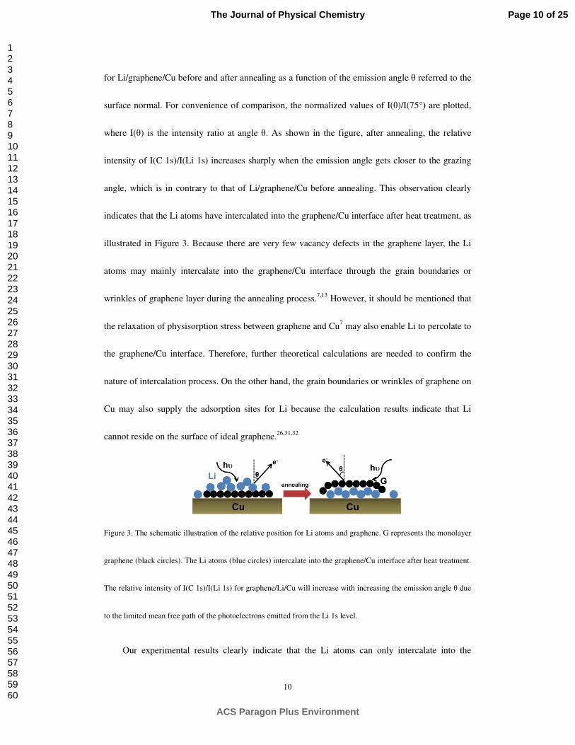
where I(θ) is the intensity ratio at angle θ. As shown in the figure, after annealing, the relative
intensity of I(C 1s)/I(Li 1s) increases sharply when the emission angle gets closer to the grazing
angle, which is in contrary to that of Li/graphene/Cu before annealing. This observation clearly
indicates that the Li atoms have intercalated into the graphene/Cu interface after heat treatment, as
illustrated in Figure 3. Because there are very few vacancy defects in the graphene layer, the Li
atoms may mainly intercalate into the graphene/Cu interface through the grain boundaries or
wrinkles of graphene layer during the annealing process.7,13 However, it should be mentioned that
the relaxation of physisorption stress between graphene and Cu7 may also enable Li to percolate to
the graphene/Cu interface. Therefore, further theoretical calculations are needed to confirm the
nature of intercalation process. On the other hand, the grain boundaries or wrinkles of graphene on
Cu may also supply the adsorption sites for Li because the calculation results indicate that Li
cannot reside on the surface of ideal graphene.26,31,32
Figure 3. The schematic illustration of the relative position for Li atoms and graphene. G represents the monolayer
graphene (black circles). The Li atoms (blue circles) intercalate into the graphene/Cu interface after heat treatment.
The relative intensity of I(C 1s)/I(Li 1s) for graphene/Li/Cu will increase with increasing the emission angle θ due
to the limited mean free path of the photoelectrons emitted from the Li 1s level.
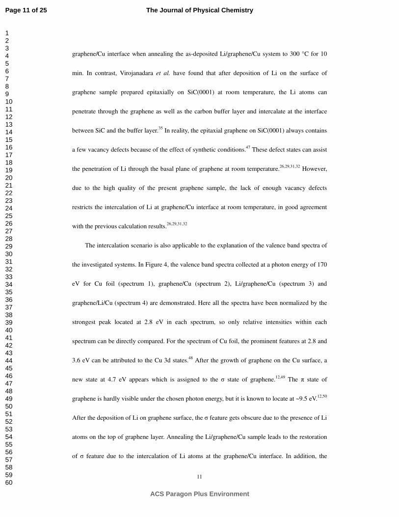
Our experimental results clearly indicate that the Li atoms can only intercalate into the
Page 10 of 25
ACS Paragon Plus Environment
The Journal of Physical Chemistry
123456789101112131415161718192021222324252627282930313233343536373839404142434445464748495051525354555657585960
11
graphene/Cu interface when annealing the as-deposited Li/graphene/Cu system to 300 °C for 10
min. In contrast, Virojanadara et al. have found that after deposition of Li on the surface of
graphene sample prepared epitaxially on SiC(0001) at room temperature, the Li atoms can
penetrate through the graphene as well as the carbon buffer layer and intercalate at the interface
between SiC and the buffer layer.35 In reality, the epitaxial graphene on SiC(0001) always contains
a few vacancy defects because of the effect of synthetic conditions.47 These defect states can assist
the penetration of Li through the basal plane of graphene at room temperature.26,29,31,32 However,
due to the high quality of the present graphene sample, the lack of enough vacancy defects
restricts the intercalation of Li at graphene/Cu interface at room temperature, in good agreement
with the previous calculation results.26,29,31,32
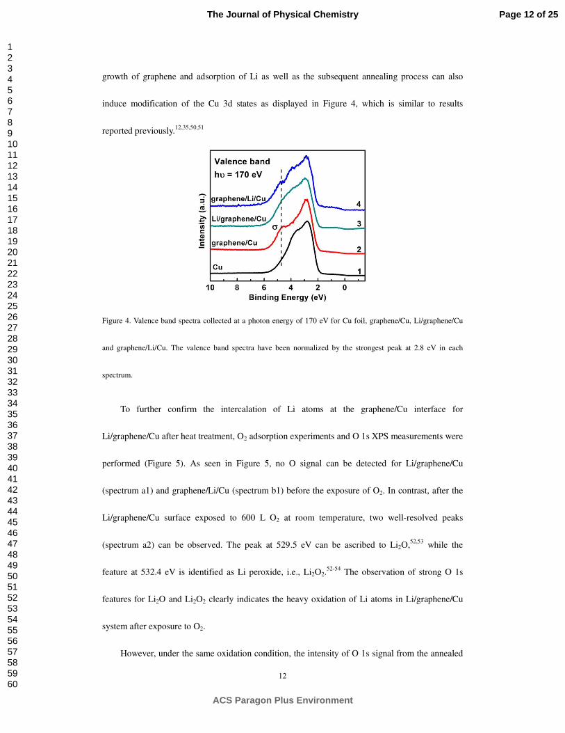
The intercalation scenario is also applicable to the explanation of the valence band spectra of
the investigated systems. In Figure 4, the valence band spectra collected at a photon energy of 170
eV for Cu foil (spectrum 1), graphene/Cu (spectrum 2), Li/graphene/Cu (spectrum 3) and
graphene/Li/Cu (spectrum 4) are demonstrated. Here all the spectra have been normalized by the
strongest peak located at 2.8 eV in each spectrum, so only relative intensities within each
spectrum can be directly compared. For the spectrum of Cu foil, the prominent features at 2.8 and
3.6 eV can be attributed to the Cu 3d states.48 After the growth of graphene on the Cu surface, a
new state at 4.7 eV appears which is assigned to the σ state of graphene.12,49 The π state of
graphene is hardly visible under the chosen photon energy, but it is known to locate at ~9.5 eV.12,50
After the deposition of Li on graphene surface, the σ feature gets obscure due to the presence of Li
atoms on the top of graphene layer. Annealing the Li/graphene/Cu sample leads to the restoration
of σ feature due to the intercalation of Li atoms at the graphene/Cu interface. In addition, the
Page 11 of 25
ACS Paragon Plus Environment
The Journal of Physical Chemistry
123456789101112131415161718192021222324252627282930313233343536373839404142434445464748495051525354555657585960
12
growth of graphene and adsorption of Li as well as the subsequent annealing process can also
induce modification of the Cu 3d states as displayed in Figure 4, which is similar to results
reported previously.12,35,50,51
Figure 4. Valence band spectra collected at a photon energy of 170 eV for Cu foil, graphene/Cu, Li/graphene/Cu
and graphene/Li/Cu. The valence band spectra have been normalized by the strongest peak at 2.8 eV in each
spectrum.
To further confirm the intercalation of Li atoms at the graphene/Cu interface for
Li/graphene/Cu after heat treatment, O2 adsorption experiments and O 1s XPS measurements were
performed (Figure 5). As seen in Figure 5, no O signal can be detected for Li/graphene/Cu
(spectrum a1) and graphene/Li/Cu (spectrum b1) before the exposure of O2. In contrast, after the
Li/graphene/Cu surface exposed to 600 L O2 at room temperature, two well-resolved peaks
(spectrum a2) can be observed. The peak at 529.5 eV can be ascribed to Li2O,52,53 while the
feature at 532.4 eV is identified as Li peroxide, i.e., Li2O2.52-54 The observation of strong O 1s
features for Li2O and Li2O2 clearly indicates the heavy oxidation of Li atoms in Li/graphene/Cu
system after exposure to O2.
However, under the same oxidation condition, the intensity of O 1s signal from the annealed
Page 12 of 25
ACS Paragon Plus Environment
The Journal of Physical Chemistry
123456789101112131415161718192021222324252627282930313233343536373839404142434445464748495051525354555657585960

13
Li/graphene/Cu sample (spectrum b2) is much weaker as compared with that of Li/graphene/Cu
(spectrum a2). This observation suggests that most of the Li atoms are hidden for exposing to
oxygen and they must have intercalated into the graphene/Cu interface after annealing, leading to
the formation of an oxidation–resistive system: graphene/Li/Cu. The passivation of Li atoms in
graphene/Li/Cu to the oxidation environment also indicates that no O2 can penetrate through the
graphene layer to react with the interfacial Li atoms.12,50 The weak O 1s signal of graphene/Li/Cu
after exposure to O2 may have two possible origins: (1) the adsorbed O2 on graphene surface;12
and (2) the oxidation of Li atoms located at the bare Cu surface which is not covered by graphene,
because this part of Li atoms could not intercalate into the graphene/Cu interface during the
annealing process.13
Figure 5. O 1s XPS spectra of Li/graphene/Cu (a) and graphene/Li/Cu (b) before and after exposed to 600 L O2 at
room temperature.
The Li 1s spectra recorded with a photon energy of 170 eV accompanied with their peak
fittings for Li/graphene/Cu and annealed Li/graphene/Cu (i.e., graphene/Li/Cu) before and after
exposed to 600 L O2 at room temperature are shown in Figure 6. The Li 1s spectra before the
Page 13 of 25
ACS Paragon Plus Environment
The Journal of Physical Chemistry
123456789101112131415161718192021222324252627282930313233343536373839404142434445464748495051525354555657585960

14
exposure of O2 can be fitted with three components, which are labeled as L1, L2 and L3,
respectively. In contrast, the spectra of Li 1s after exposed to O2 are fitted with four components
(L1, L2, L3 and L4) due to the oxidation of Li. In the fitting procedure, the values of full width at
half maximum (FWHM) for L1, L2 and L3 components were constrained to a maximum of 1.6 eV.
The fitted results show that the FWHM of L1 component is 1.0 ± 0.2 eV, while those of L2 and L3
components are 1.5 ± 0.1 eV. The different FWHMs for the Li species may be caused by their
different chemical environments. For the L4 component, the FWHM is ~1.7 eV (see below for
detail).
Figure 6. SRPES spectra of Li 1s collected at 170 eV photon energy as well as their peak fittings for
Li/graphene/Cu and graphene/Li/Cu before and after exposed to 600 L O2 at room temperature. The black open
circles are the experimental data. The red lines indicate the sum of individual components. The Li 1s spectra before
the exposure of O2 can be fitted with three components, while the spectra after exposed to O2 are fitted with four
components due to the oxidation of Li. The L1, L2, L3 and L4 represent different Li species as described in the
Page 14 of 25
ACS Paragon Plus Environment
The Journal of Physical Chemistry
123456789101112131415161718192021222324252627282930313233343536373839404142434445464748495051525354555657585960
15
text.
From the fits to Li 1s spectra we can see that the L1, L2 and L3 components are well resolved
in all the Li 1s spectra. The L1 component is suggested to correspond to the Li atoms directly
located on the bare Cu surface uncovered by graphene as we have stated above.55,56 The L2
component is assigned to the metallic Li,21,53 while the L3 component is ascribed to the Li atoms
interacting with the graphene layer.35,45
However, compared with the spectrum of Li/graphene/Cu (spectrum 1), the intensities of L2
and L3 components are reduced and almost no intensity change can be observed for the L1
component in the spectrum of graphene/Li/Cu (spectrum 2). This is because the Li atoms of L2
and L3 components have intercalated into the graphene/Cu interface during the annealing process
and the graphene layer staying on top of them can attenuate their peak intensities.35 Because the Li
atoms ascribed to the L1 component do not penetrate into the graphene/Cu interface under the heat
treatment condition, there should be no intensity change for the L1 component before and after
annealing, in good agreement with our experimental results.
After exposing the Li/graphene/Cu sample to 600 L O2, the intensities of L2 and L3
components in the Li 1s spectrum (spectrum 3) decrease significantly. In contrast, a broad feature
L4 appears at 55.3 eV, which can be ascribed to the Li in Li2O and Li2O2.53,54 These results
indicate that the Li atoms of L2 and L3 components have been seriously oxidized after such
oxygen treatment, which is consistent with the O 1s results discussed above. Here, it should be
noted that the Li 1s binding energy difference of Li2O and Li2O2 are very small53,54 and due to the
relative low spectral resolution in the present case, we fitted the oxidized Li species with only one
broad peak (FWHM ~1.7 eV).
Page 15 of 25
ACS Paragon Plus Environment
The Journal of Physical Chemistry
123456789101112131415161718192021222324252627282930313233343536373839404142434445464748495051525354555657585960
16
In contrast, the Li 1s spectrum of graphene/Li/Cu under the same oxidation condition
(spectrum 4) is totally different from that of Li/graphene/Cu (spectrum 3), and comparable with
the one for graphene/Li/Cu before O2 exposure (spectrum 2), indicative of the weak or no
oxidation of intercalated Li atoms after the exposure of O2. However, some changes can still be
clearly distinguished for the Li 1s spectra of graphene/Li/Cu before and after O2 exposure when
comparing the spectra 2 and 4: (a) the intensity of L1 component reduces considerably and a weak
L4 component appears after the O2 exposure, which are caused by the oxidation of Li atoms
without the protection of graphene as discussed above; and (b) the relative intensity of L2 and L3
[I(L2)/I(L3)] increases after the exposure of O2. We are still not clear about the exact origin of this
phenomenon and further theoretical work is needed to address this question. Here, we tentatively
attribute it to the weakened interaction between graphene and Li induced by the adsorption of O2
on graphene surface, which may result in the increment of metallic Li (L2 component) intensity
and thus the increase of I(L2)/I(L3).12,13 Overall, the Li 1s results are in good agreement with the
C 1s and O 1s results, further confirming the intercalation of Li at the graphene/Cu interface after
the annealing process.
Figure 7 presents a set of Cu 2p XPS spectra from graphene/Cu (spectrum 1),
Li/graphene/Cu (spectrum 2), graphene/Li/Cu (spectrum 3), and the latter two systems after the
exposure of O2 under the conditions mentioned above (spectra 4 and 5). As seen, the deposition of
Li on graphene surface leads to a reduction of the Cu 2p peak intensity immediately. However, no
intensity changes can be observed for Li/graphene/Cu before and after the heat treatment, which
supports the hypothesis of Li intercalation into the graphene/Cu interface to form graphene/Li/Cu
structure after annealing. Moreover, we can rule out the sintering process of Li atoms occurred on
Page 16 of 25
ACS Paragon Plus Environment
The Journal of Physical Chemistry
123456789101112131415161718192021222324252627282930313233343536373839404142434445464748495051525354555657585960

17
top of graphene layer during annealing because otherwise the increase of the Cu 2p intensity
should be observed. During the whole sample treatment process (both annealing and O2 exposure),
no peak shift or appearance of new peaks has been found. This indicates that the interaction
between Li and O2 with Cu in our case should be very weak55 and graphene/Cu can be a good
candidate for the fabrication of oxidation-resistivity Li-intercalated graphene system.
Figure 7. Cu 2p XPS spectra of Li/graphene/Cu and graphene/Li/Cu, before and after exposed to 600 L O2 at room
temperature. For comparison, the Cu 2p spectrum of graphene/Cu is also shown as the reference.
CONCLUSIONS
In conclusion, we have studied the adsorption of Li atoms on the monolayer graphene sample
prepared on the Cu foil and the intercalation of Li atoms into the graphene/Cu interface. Our
results indicate that the deposition of Li on the graphene surface leads to charge transfer from Li to
graphene overlayer. The Li atoms can intercalate into the graphene/Cu interface when annealing
the as-deposited Li/graphene/Cu system at 300 ºC. Due to the protection of graphene layer on-top,
exposure of the formed graphene/Li/Cu system to O2 environment does not lead to the oxidation
of the intercalated Li atoms. The successful in situ fabrication of Li-intercalated graphene/metal
Page 17 of 25
ACS Paragon Plus Environment
The Journal of Physical Chemistry
123456789101112131415161718192021222324252627282930313233343536373839404142434445464748495051525354555657585960
18
compound can facilitate the development of nanoscale Li-ion batteries based on epitaxially grown
graphene in the future.
ACKNOWLEDGEMENTS
This work was financially supported by the National Natural Science Foundation of China
(Grant No.21173200), National Basic Research Program of China (2010CB923302,
2013CB834605), and the Specialized Research Fund for the Doctoral Program of Higher
Education of Ministry of Education (Grant No. 20113402110029). L. Zhang thanks the financial
support from the Scholarship Award for Excellent Doctoral Student Granted by Ministry of
Education of China.
REFERENCES
(1) Novoselov, K. S.; Geim, A. K.; Morozov, S. V.; Jiang, D.; Zhang, Y.; Dubonos, S. V.; Grigorieva, I.
V.; Firsov, A. A. Electric Field Effect in Atomically Thin Carbon Films. Science 2004, 306, 666-669.
(2) Geim, A. K. Graphene: Status and Prospects. Science 2009, 324, 1530-1534.
(3) Li, X. S., Cai, W. W., An, J. H., Kim, S., Nah, J., Yang, D. X., Piner, R., Velamakanni, A., Jung, I.,
Tutuc, E.; et al. Large-Area Synthesis of High-Quality and Uniform Graphene Films on Copper Foils.
Science 2009, 324, 1312-1314.
(4) Eom, D.; Prezzi, D.; Rim, K. T.; Zhou, H.; Lefenfeld, M.; Xiao, S.; Nuckolls, C.; Hybertsen, M.
S.; Heinz, T. F.; Flynn, G. W. Structure and Electronic Properties of Graphene Nanoislands on Co(0001).
Nano Lett. 2009, 9, 2844-2848.
(5) Sutter, P. W.; Flege, J. I.; Sutter, E. A. Epitaxial Graphene on Ruthenium. Nat. Mater. 2008, 7,
Page 18 of 25
ACS Paragon Plus Environment
The Journal of Physical Chemistry
123456789101112131415161718192021222324252627282930313233343536373839404142434445464748495051525354555657585960

19
406-411.
(6) Voloshina, E.; Dedkov, Y. Graphene on Metallic Surfaces: Problems and Perspectives. Phys.
Chem. Chem. Phys. 2012, 14, 13502-13514.
(7) Mattevi, C.; Kim, H.; Chhowalla, M. A Review of Chemical Vapour Deposition of Graphene on
Copper. J. Mater. Chem. 2011, 21, 3324-3334.
(8) Bae, S., Kim, H., Lee, Y., Xu, X. F., Park, J. S., Zheng, Y., Balakrishnan, J., Lei, T., Kim, H. R.,
Song, Y. I.; et al. Roll-to-Roll Production of 30-Inch Graphene Films for Transparent Electrodes. Nature
Nanotech. 2010, 5, 574-578.
(9) Nagashima, A.; Tejima, N.; Oshima, C. Electronic States of the Pristine and Alkali-Metal
Intercalted Monolayer Graphite/Ni(111) Systems. Phys. Rev. B 1994, 50, 17487-17495.
(10) Shikin, A. M.; Prudnikova, G. V.; Adamchuk, V. K.; Moresco, F.; Rieder, K. H. Surface
Intercalation of Gold underneath a Graphite Monolayer on Ni(111) Studied by Angle-Resolved
Photoemission and High-Resolution Electron-Energy-Loss Spectroscopy. Phys. Rev. B 2000, 62,
13202-13208.
(11) Dedkov, Y. S.; Shikin, A. M.; Adamchuk, V. K.; Molodtsov, S. L.; Laubschat, C.; Bauer, A.;
Kaindl, G. Intercalation of Copper underneath a Monolayer of Graphite on Ni(111). Phys. Rev. B 2001,
64, 035405.
(12) Dedkov, Y. S.; Fonin, M.; Rüdiger, U.; Laubschat, C. Graphene-Protected Iron Layer on Ni(111).
Appl. Phys. Lett. 2008, 93, 022509.
(13) Jin, L.; Fu, Q.; Mu, R. T.; Tan, D. L.; Bao, X. H. Pb Intercalation underneath a Graphene Layer on
Ru(0001) and Its Effect on Graphene Oxidation. Phys. Chem. Chem. Phys. 2011, 13, 16655-16660.
(14) Addou, R.; Dahal, A.; Batzill, M. Graphene on Ordered Ni-Alloy Surfaces Formed by Metal (Sn,
Page 19 of 25
ACS Paragon Plus Environment
The Journal of Physical Chemistry
123456789101112131415161718192021222324252627282930313233343536373839404142434445464748495051525354555657585960

20
Al) Intercalation between Graphene/Ni(111). Surf. Sci. 2012, 606, 1108-1112.
(15) Gyamfi, M.; Eelbo, T.; Waśniowska, M.; Wiesendanger, R. Impact of Intercalated Cobalt on the
Electronic Properties of Graphene on Pt(111). Phys. Rev. B 2012, 85, 205434.
(16) Varykhalov, A.; Sanchez-Barriga, J.; Shikin, A. M.; Biswas, C.; Vescovo, E.; Rybkin, A.;
Marchenko, D.; Rader, O. Electronic and Magnetic Properties of Quasifreestanding Graphene on Ni.
Phys. Rev. Lett. 2008, 101, 157601.
(17) Haddon, R. C., Hebard, A. F., Rosseinsky, M. J., Murphy, D. W., Duclos, S. J., Lyons, K. B.,
Miller, B., Rosamilia, J. M., Fleming, R. M., Kortan, A. R.; et al. Conducting Films of C60 and C70 by
Alkali-Metal Doping. Nature 1991, 350, 320-322.
(18) Caragiu, M.; Finberg, S. Alkali Metal Adsorption on Graphite: A Review. J. Phys.: Condens. Mat.
2005, 17, R995-R1024.
(19) Harilal, S. S.; Allain, J. P.; Hassanein, A.; Hendricks, M. R.; Nieto-Perez, M. Reactivity of
Lithium Exposed Graphite Surface. Appl. Surf. Sci. 2009, 255, 8539-8543.
(20) Deng, W. Q.; Xu, X.; Goddard, W. A. New Alkali Doped Pillared Carbon Materials Designed to
Achieve Practical Reversible Hydrogen Storage for Transportation. Phys. Rev. Lett. 2004, 92.
(21) Wertheim, G. K.; Vanattekum, P.; Basu, S. Electronic Structure of Lithium Graphite. Solid State
Commun. 1980, 33, 1127-1130.
(22) Hu, Z. P.; Ignatiev, A. Lithium Adsorption on the Graphite(0001) Surface. Phys. Rev. B 1984, 30,
4856-4859.
(23) Kganyago, K. R.; Ngoepe, P. E. Structural and Electronic Properties of Lithium Intercalated
Graphite LiC6. Phys. Rev. B 2003, 68, 205111.
(24) Valencia, F.; Romero, A. H.; Ancilotto, F.; Silvestrelli, P. L. Lithium Adsorption on Graphite from
Page 20 of 25
ACS Paragon Plus Environment
The Journal of Physical Chemistry
123456789101112131415161718192021222324252627282930313233343536373839404142434445464748495051525354555657585960

21
Density Functional Theory Calculations. J. Phys. Chem. B 2006, 110, 14832-14841.
(25) Titantah, J. T.; Lamoen, D.; Schowalter, M.; Rosenauer, A. Density-Functional Theory
Calculations of the Electron Energy-Loss Near-Edge Structure of Li-intercalated graphite. Carbon 2009,
47, 2501-2510.
(26) Lee, E.; Persson, K. A. Li Absorption and Intercalation in Single Layer Graphene and Few Layer
Graphene by First Principles. Nano Lett. 2012, 12, 4624-4628.
(27) Boukhvalov, D. W.; Virojanadara, C. Penetration of Alkali Atoms throughout a Graphene
Membrane: Theoretical Modeling. Nanoscale 2012, 4, 1749-1753.
(28) Kaloni, T. P.; Cheng, Y. C.; Kahaly, M. U.; Schwingenschlogl, U. Charge Carrier Density in
Li-Intercalated Graphene. Chem. Phys. Lett. 2012, 534, 29-33.
(29) Fan, X.; Zheng, W. T.; Kuo, J. L. Adsorption and Diffusion of Li on Pristine and Defective
Graphene. ACS Appl. Mater. Interfaces 2012, 4, 2432-2438.
(30) Khantha, M.; Cordero, N. A.; Molina, L. M.; Alonso, J. A.; Girifalco, L. A. Interaction of Lithium
with Graphene: An ab initio Study. Phys. Rev. B 2004, 70, 125422.
(31) Yao, F.; Gunes, F.; Ta, H. Q.; Lee, S. M.; Chae, S. J.; Sheem, K. Y.; Cojocaru, C. S.; Xie, S. S.;
Lee, Y. H. Diffusion Mechanism of Lithium Ion through Basal Plane of Layered Graphene. J. Am.
Chem. Soc. 2012, 134, 8646-8654.
(32) Li, Y.; Zhou, G.; Li, J.; Wu, J.; Gu, B.-L.; Duan, W. Lithium Intercalation Induced Decoupling of
Epitaxial Graphene on SiC(0001): Electronic Property and Dynamic Process. J. Phys. Chem. C 2011,
115, 23992-23997.
(33) Radhakrishnan, G.; Cardema, J. D.; Adams, P. M.; Kim, H. I.; Foran, B. Fabrication and
Electrochemical Characterization of Single and Multi-Layer Graphene Anodes for Lithium-Ion
Page 21 of 25
ACS Paragon Plus Environment
The Journal of Physical Chemistry
123456789101112131415161718192021222324252627282930313233343536373839404142434445464748495051525354555657585960

22
Batteries. J. Electrochem. Soc. 2012, 159, A752-A761.
(34) Pollak, E.; Geng, B.; Jeon, K. J.; Lucas, I. T.; Richardson, T. J.; Wang, F.; Kostecki, R. The
Interaction of Li+ with Single-Layer and Few-Layer Graphene. Nano Lett. 2010, 10, 3386-3388.
(35) Virojanadara, C.; Watcharinyanon, S.; Zakharov, A. A.; Johansson, L. I. Epitaxial Graphene on
6H-SiC and Li intercalation. Phys. Rev. B 2010, 82, 205402.
(36) Ohta, T.; Bostwick, A.; Seyller, T.; Horn, K.; Rotenberg, E. Controlling the Electronic Structure of
Bilayer Graphene. Science 2006, 313, 951-954.
(37) Riedl, C.; Coletti, C.; Iwasaki, T.; Zakharov, A. A.; Starke, U. Quasi-Free-Standing Epitaxial
Graphene on SiC Obtained by Hydrogen Intercalation. Phys. Rev. Lett. 2009, 103, 246804.
(38) Wang, G. D.; Kong, D. D.; Pan, Y. H.; Pan, H. B.; Zhu, J. F. Low Energy Ar-ion Bombardment
Effects on the CeO2 Surface. Appl. Surf. Sci. 2012, 258, 2057-2061.
(39) Li, X.; Magnuson, C. W.; Venugopal, A.; Tromp, R. M.; Hannon, J. B.; Vogel, E. M.; Colombo, L.;
Ruoff, R. S. Large-Area Graphene Single Crystals Grown by Low-Pressure Chemical Vapor Deposition
of Methane on Copper. J. Am. Chem. Soc. 2011, 133, 2816-2819.
(40) Ferrari, A. C., Meyer, J. C., Scardaci, V., Casiraghi, C., Lazzeri, M., Mauri, F., Piscanec, S., Jiang,
D., Novoselov, K. S., Roth, S.; et al. Raman Spectrum of Graphene and Graphene Layers. Phys. Rev.
Lett. 2006, 97, 187401.
(41) Wang, Y. Y.; Ni, Z. H.; Yu, T.; Shen, Z. X.; Wang, H. M.; Wu, Y. H.; Chen, W.; Wee, A. T. S.
Raman Studies of Monolayer Graphene: The Substrate Effect. J. Phys. Chem. C 2008, 112,
10637-10640.
(42) Wu, Y. P., Chou, H., Ji, H. X., Wu, Q. Z., Chen, S. S., Jiang, W., Hao, Y. F., Kang, J. Y., Ren, Y. J.,
Piner, R. D.; et al. Growth Mechanism and Controlled Synthesis of AB-Stacked Bilayer Graphene on
Page 22 of 25
ACS Paragon Plus Environment
The Journal of Physical Chemistry
123456789101112131415161718192021222324252627282930313233343536373839404142434445464748495051525354555657585960

23
Cu-Ni Alloy Foils. Acs Nano 2012, 6, 7731-7738.
(43) Yan, Z.; Peng, Z. W.; Sun, Z. Z.; Yao, J.; Zhu, Y.; Liu, Z.; Ajayan, P. M.; Tour, J. M. Growth of
Bilayer Graphene on Insulating Substrates. Acs Nano 2011, 5, 8187-8192.
(44) Costa, S. D.; Righi, A.; Fantini, C.; Hao, Y.; Magnuson, C.; Colombo, L.; Ruoff, R. S.; Pimenta,
M. A. Resonant Raman Spectroscopy of Graphene Grown on Copper Substrates. Solid State Commun.
2012, 152, 1317-1320.
(45) Mordkovich, V. Z. Synthesis and XPS Investigation of Superdense Lithium-Graphite Intercalation
Compound, LiC2. Synthetic. Met. 1996, 80, 243-247.
(46) Deshpande, M.; Kanhere, D.; Vasiliev, I.; Martin, R. Density-Functional Study of Structural and
Electronic Properties of NanLi and LinNa (1 ≤ n ≤ 12) Clusters. Phys. Rev. A 2002, 65, 033202.
(47) Rutter, G. M.; Crain, J. N.; Guisinger, N. P.; Li, T.; First, P. N.; Stroscio, J. A. Scattering and
Interference in Epitaxial Graphene. Science 2007, 317, 219-222.
(48) Wagner, L. F.; Spicer, W. E.; Doniach, S. Nature of Energy Dependent Self Energy for
Photoelectrons in Copper. Solid State Commun. 1974, 15, 669-672.
(49) Dedkov, Y. S.; Fonin, M.; Laubschat, C. A Possible Source of Spin-Polarized Electrons: The Inert
Graphene/Ni(111) System. Appl. Phys. Lett. 2008, 92, 052506.
(50) Cui, Y.; Gao, J.; Jin, L.; Zhao, J.; Tan, D.; Fu, Q.; Bao, X. An Exchange Intercalation Mechanism
for the Formation of a Two-Dimensional Si Structure underneath Graphene. Nano Res. 2012, 5,
352-360.
(51) Siokou, A.; Ravani, F.; Karakalos, S.; Frank, O.; Kalbac, M.; Galiotis, C. Surface Refinement and
Electronic Properties of Graphene Layers Grown on Copper Substrate: An XPS, UPS and EELS Study.
Appl. Surf. Sci. 2011, 257, 9785-9790.
Page 23 of 25
ACS Paragon Plus Environment
The Journal of Physical Chemistry
123456789101112131415161718192021222324252627282930313233343536373839404142434445464748495051525354555657585960

24
(52) Qiu, S. L.; Lin, C. L.; Chen, J.; Strongin, M. Photoemission Studies of the Interaction of Li and
Solid Molecular Oxygen. Phys. Rev. B 1989, 39, 6194-6197.
(53) Shek, M. L.; Hrbek, J.; Sham, T. K.; Xu, G. Q. A Soft-X-Ray Study of the Interaction of Oxygen
with Li Surf. Sci. 1990, 234, 324-334.
(54) Wu, Q.-H.; Thissen, A.; Jaegermann, W. Photoelectron Spectroscopic Study of Li Oxides on Li
Over-Deposited V2O5 Thin Film Surfaces. Appl. Surf. Sci. 2005, 250, 57-62.
(55) Carlsson, A.; Claesson, D.; Katrich, G.; Lindgren, S. Å.; Walldén, L. Observation of Structure
Changes for Li/Cu(111) by Photoemission from Li Core and Quantum-Well States. Phys. Rev. B 1998,
57, 13192-13198.
(56) Shek, M. L.; Hrbek, J.; Sham, T. K.; Xu, G. Q. Core-Level Photoemission from Alkali-Metals on
Ru(001). Phys. Rev. B 1990, 41, 3447-3454.
Page 24 of 25
ACS Paragon Plus Environment
The Journal of Physical Chemistry
123456789101112131415161718192021222324252627282930313233343536373839404142434445464748495051525354555657585960
25
TABLE OF CONTENT
Page 25 of 25
ACS Paragon Plus Environment
The Journal of Physical Chemistry
123456789101112131415161718192021222324252627282930313233343536373839404142434445464748495051525354555657585960