electrochemical intercalation of lithium ions into nbse ...davydov/16hitz_nbse2 li-intercal... ·...
TRANSCRIPT
Electrochemical Intercalation of Lithium Ions into NbSe2 NanosheetsEmily Hitz,†,⊥ Jiayu Wan,†,⊥ Anand Patel,‡ Yue Xu,† Louisa Meshi,‡,§ Jiaqi Dai,† Yanan Chen,†
Aijiang Lu,† Albert V. Davydov,*,‡ and Liangbing Hu*,†
†Department of Materials Science and Engineering, University of Maryland, College Park, Maryland 20742, United States‡Materials Science and Engineering Division, National Institute of Standards and Technology, Gaithersburg, Maryland 20878, UnitedStates§Department of Materials Engineering, Ben Gurion University of the Negev, Beer Sheva 84105, Israel
ABSTRACT: Transition metal dichalcogenides (TMDCs)have been known for decades to have unique properties andrecently attracted broad attention for their two-dimensional(2D) characteristics. NbSe2 is a metallic TMDC that has beenstudied for its charge density wave transition behavior andsuperconductivity but is still largely unexplored for its potentialuse in engineered devices with applications in areas such aselectronics, optics, and batteries. Thus, we successfullydemonstrate and present evidence of lithium intercalation inNbSe2 as a technique capable of modifying the materialproperties of NbSe2 for further study. We demonstratesuccessful intercalation of Li ions into NbSe2 and confirmthis result through X-ray diffraction, noting a unit cell size increase from 12.57 to 13.57 Å in the c lattice parameter of the NbSe2after intercalation. We also fabricate planar half-cell electrochemical devices using ultrathin NbSe2 from platelets to observeevidence of Li-ion intercalation through an increase in the optical transmittance of the material in the visible range. Using 550 nmwavelength light, we observed an increase in optical transmittance of 26% during electrochemical intercalation.
KEYWORDS: electrochemical intercalation, niobium selenide, 2D materials, lithium, transparent electrodes
■ INTRODUCTION
A class of materials known as transition metal dichalcogenides(TMDCs) has been under renewed study due to recentadvancements made in the area of layered two-dimensional(2D) materials, particularly with graphitic films for applicationsin electronics, optoelectronics, and electrochemical devices.1−5
As layered materials, TMDCs are known to exhibit a widerange of unique mechanical, electrical, and chemical propertiesthat rival the advanced performance standards of other 2Dmaterials such as graphene and BN.6−15 While TMDCs havebeen under study for decades, efforts within the scientific andengineering community to study the properties of these uniquematerials have strengthened again in large part due to recentadvances in sample preparation and handling of 2Dmaterials.16−20
Many layered materials have been found to participate in aprocess called intercalation, which allows various molecules tobe inserted and stored within a host crystal structure.21−27
These materials, especially in their 2D morphology, can provideenergy storage capabilities28 while also having the potential tomeet concerns that are specific to the modern world, that is,their extraordinary optoelectronic properties29−31 and mechan-ical flexibility.32,33 Intercalation has been used as a technique tofurther enhance the properties of these materials for theiroptical, thermal, magnetic, and electronic behavior.34−41
TMDCs are materials composed of stacks of atomically thinsheets having the chemical form MX2, in which M is atransition metal (W, Mo, Nb) and X is a chalcogen (S, Se, Te).For NbSe2, each constituent nanosheet has hexagonal structurein which one atomic layer of niobium is sandwiched betweentwo atomic layers of selenium. Atoms are covalently bondedwithin the three-atom-thick layers, while van der Waals forcesbetween the layers allow them to remain together. NbSe2 hasmetallic conductivity at ambient conditions with superconduct-ing and charge density wave transitions at low temper-atures.42−44 Compared to its 2D “cousin” graphene, NbSe2 isstill largely unexplored for its chemical and physical proper-ties.45,46
In this work, we demonstrate a viable and accessibletechnique for modifying the properties of 2D NbSe2 to allowfor greater depth of study of the material’s thermal, chemical,and optical behavior. Our approach relies upon electrochemicalintercalation of an alkali metal ion, in this case lithium, into alayered material, which gives rise to specific optical andchemical changes.47,48 We provide evidence of these changesand characterization of the material system through high-resolution transmission electron microscopy (HRTEM),
Received: November 28, 2015Accepted: April 21, 2016Published: April 21, 2016
Research Article
www.acsami.org
© 2016 American Chemical Society 11390 DOI: 10.1021/acsami.5b11583ACS Appl. Mater. Interfaces 2016, 8, 11390−11395
electrochemical investigations, optical microscopy, and X-raydiffraction (XRD) methods.
■ RESULTS AND DISCUSSIONFor this investigation, we synthesized layered NbSe2 in bothpowder and platelet form via the chemical vapor transportmethod. The NbSe2 powder was used as the active material incoin cell electrodes for electrochemical testing (Figure 1a,b),
while single-crystal NbSe2 platelets were used to fabricateplanar devices for observation of the optical behavior of thematerial. A detailed enumeration of relevant techniques can befound in the Experimental Procedures section.It is well-documented in previous research efforts on 2D
materials that the electrochemical processes associated withlithium intercalation in TMDCs are often complex, involvingboth reversible and nonreversible reactions and having multiplelithiation/delithiation stages. With the likelihood of a complexsystem taken into consideration, our goal was to study thestructural and compositional behavior of the electrochemicallithiation process in NbSe2. We first performed cycling andcyclic voltammetry (CV) electrochemical studies on coin cells(half cell with Li as counter electrode) containing an NbSe2-based cathode in the voltage range of 0−3 V, which was foundto have many stages of lithiation reactions present. We excludethis regime from our focus of discussion. After furtherelectrochemical studies, it was found that cycling the coincells within the voltage range of 1−3 V allowed the system tostay within a simpler lithiation/delithiation regime. To
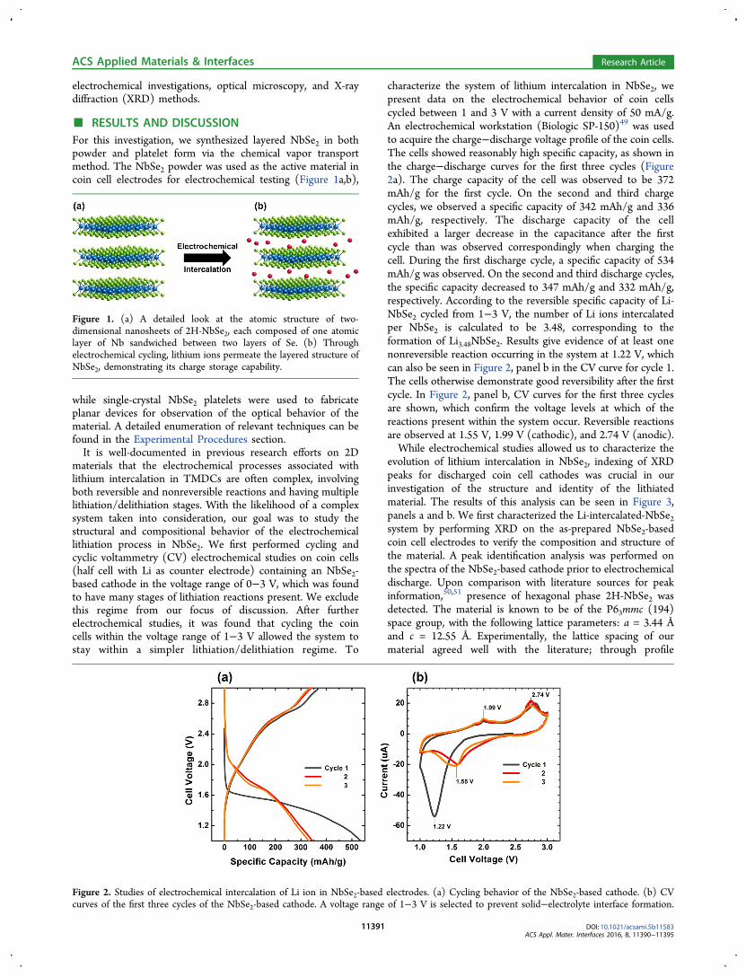
characterize the system of lithium intercalation in NbSe2, wepresent data on the electrochemical behavior of coin cellscycled between 1 and 3 V with a current density of 50 mA/g.An electrochemical workstation (Biologic SP-150)49 was usedto acquire the charge−discharge voltage profile of the coin cells.The cells showed reasonably high specific capacity, as shown inthe charge−discharge curves for the first three cycles (Figure2a). The charge capacity of the cell was observed to be 372mAh/g for the first cycle. On the second and third chargecycles, we observed a specific capacity of 342 mAh/g and 336mAh/g, respectively. The discharge capacity of the cellexhibited a larger decrease in the capacitance after the firstcycle than was observed correspondingly when charging thecell. During the first discharge cycle, a specific capacity of 534mAh/g was observed. On the second and third discharge cycles,the specific capacity decreased to 347 mAh/g and 332 mAh/g,respectively. According to the reversible specific capacity of Li-NbSe2 cycled from 1−3 V, the number of Li ions intercalatedper NbSe2 is calculated to be 3.48, corresponding to theformation of Li3.48NbSe2. Results give evidence of at least onenonreversible reaction occurring in the system at 1.22 V, whichcan also be seen in Figure 2, panel b in the CV curve for cycle 1.The cells otherwise demonstrate good reversibility after the firstcycle. In Figure 2, panel b, CV curves for the first three cyclesare shown, which confirm the voltage levels at which of thereactions present within the system occur. Reversible reactionsare observed at 1.55 V, 1.99 V (cathodic), and 2.74 V (anodic).While electrochemical studies allowed us to characterize the
evolution of lithium intercalation in NbSe2, indexing of XRDpeaks for discharged coin cell cathodes was crucial in ourinvestigation of the structure and identity of the lithiatedmaterial. The results of this analysis can be seen in Figure 3,panels a and b. We first characterized the Li-intercalated-NbSe2system by performing XRD on the as-prepared NbSe2-basedcoin cell electrodes to verify the composition and structure ofthe material. A peak identification analysis was performed onthe spectra of the NbSe2-based cathode prior to electrochemicaldischarge. Upon comparison with literature sources for peakinformation,50,51 presence of hexagonal phase 2H-NbSe2 wasdetected. The material is known to be of the P63mmc (194)space group, with the following lattice parameters: a = 3.44 Åand c = 12.55 Å. Experimentally, the lattice spacing of ourmaterial agreed well with the literature; through profile
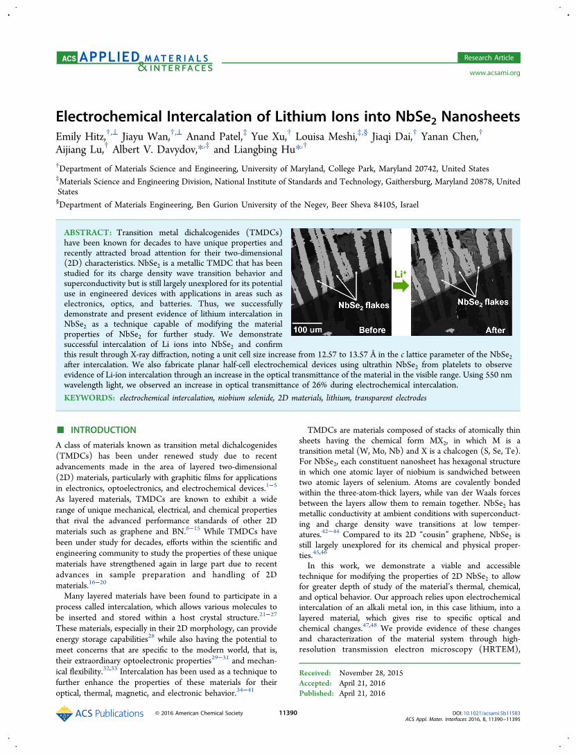
Figure 1. (a) A detailed look at the atomic structure of two-dimensional nanosheets of 2H-NbSe2, each composed of one atomiclayer of Nb sandwiched between two layers of Se. (b) Throughelectrochemical cycling, lithium ions permeate the layered structure ofNbSe2, demonstrating its charge storage capability.
Figure 2. Studies of electrochemical intercalation of Li ion in NbSe2-based electrodes. (a) Cycling behavior of the NbSe2-based cathode. (b) CVcurves of the first three cycles of the NbSe2-based cathode. A voltage range of 1−3 V is selected to prevent solid−electrolyte interface formation.
ACS Applied Materials & Interfaces Research Article
DOI: 10.1021/acsami.5b11583ACS Appl. Mater. Interfaces 2016, 8, 11390−11395
11391
matching using a Le Bail fit with (TOPAS analysis software),the NbSe2-based cathode sample was identified to have an aparameter of 3.4437(3) Å and a c parameter of 12.5668(3) Å.Elemental Cu in its cubic form was also detected. The presenceof Cu in the X-ray diffractogram can be attributed to the copperfoil current collector on which the slurry was deposited.After electrochemical discharge from the intrinsic open
circuit voltage of the cell to 1 V, we observed a preservation ofthe layered NbSe2 structure, as indicated by the results of thepeak identification. Because of the air-sensitivity of thedischarged cathodes, Kapton tape was placed over the samples,which resulted in an observation of background diffraction from
10° to 30°. Profile matching using a Le Bail fit was performedon the XRD pattern for the cell discharged to 1 V. The resultsof this analysis showed that the unit cell size of the crystalincreased upon discharge to 1 V, as a left-shift of the NbSe2peaks occurred. Most notably, the c parameter increased from12.5668(3) Å before intercalation to 13.5702(5) Å, while the aparameter remained approximately unchanged at 3.4311(2) Å.An increase in the unit cell size in the direction of the cparameter corresponds to an increase in the interlayer spacing.We attribute this change in the interlayer spacing to thepresence of lithium ions after intercalation.
Figure 3. (a) Full and (b) zoomed-in from 25° to 40°, XRD patterns of the NbSe2-based cathode with carbon black additive and PVP polymerbinder before and after electrochemical intercalation. After electrochemical discharge to 1 V, the presence of lithium via a change in the crystal unitcell size is evident, and after electrochemical discharge to 0 V, presence of Li and irreversible formation of a solid electrolyte interface layer isdemonstrated.
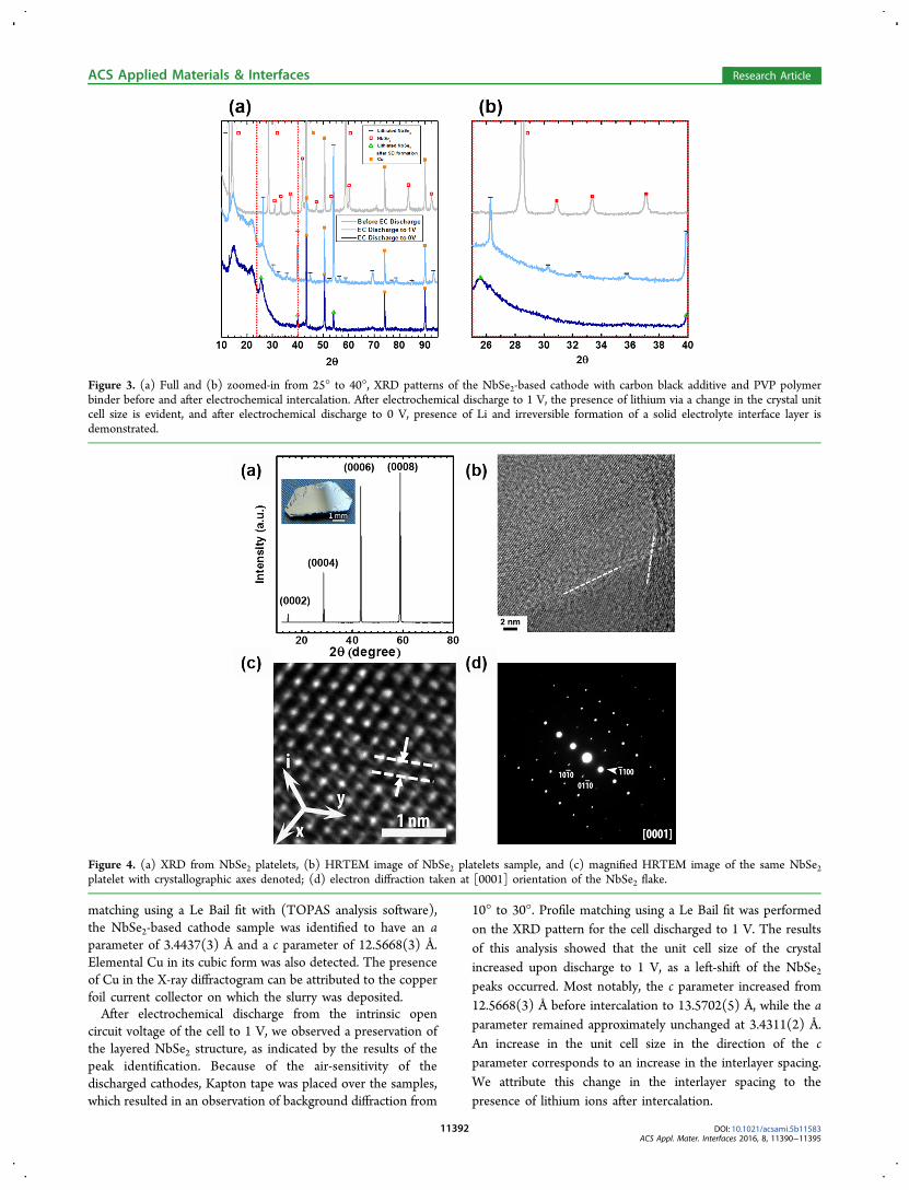
Figure 4. (a) XRD from NbSe2 platelets, (b) HRTEM image of NbSe2 platelets sample, and (c) magnified HRTEM image of the same NbSe2platelet with crystallographic axes denoted; (d) electron diffraction taken at [0001] orientation of the NbSe2 flake.
ACS Applied Materials & Interfaces Research Article
DOI: 10.1021/acsami.5b11583ACS Appl. Mater. Interfaces 2016, 8, 11390−11395
11392
As shown in Figure 3, panels a and b, electrochemicaldischarge of a cell to 0 V resulted in a very different crystalstructure than the discharge to 1 V. After peak identification, weobserved a decreased relative intensity of NbSe2 peaks to Cupeaks and an even larger left shift of NbSe2 peaks for the regionof 25° to 40° (Figure 3b). We attribute the left shift again to anincrease in the c-axis to 13.57 Å due to Li intercalation inbetween the NbSe2 layers and the lower relative intensity to thedestruction of material during large amounts of lithiation.In the previous section, we used NbSe2 powder as active
material to show that Li ion can electrochemically intercalate inthe material. To further demonstrate Li-ion intercalation in 2DNbSe2 materials and the optical and structural changes thatoccur, we prepared NbSe2 by the chemical vapor transportmethod. Figure 4, panel a inset shows the truncated trapezoid-shaped platelet with a [000l] basal facet is about 200 nm thick.The XRD peaks of the NbSe2 platelet are at 14.46°, 28.56°,43.32°, and 58.89°, which correspond to the (0002), (0004),(0006), and (0008) lattice planes of the 2H NbSe2 (P63/mmc(194); PDF#87−24015), with c lattice parameter of 12.570 Å.This XRD result clearly shows the NbSe2 platelet we preparedis single crystalline. Transmission electron microscopy (TEM)was also utilized to characterize the NbSe2 platelet. Thestoichiometry was verified using standardless X-ray energydispersive spectroscopy (EDS) in TEM. Figure 4, panel bshows the HRTEM image of the single crystalline NbSe2. Thedashed lines in the image indicate edges of areas with differentthickness, which illustrate the layered nature of the material.Figure 4, panel c shows a magnified HRTEM image of the samesample. An interplanar distance of d10.0 = 2.98 ± 0.04 Å ismarked on the image. The selected area electron diffraction(SAED) pattern of NbSe2 taken along [0001] direction isshown in Figure 4, panel d.Planar batteries were built to study the optical properties of
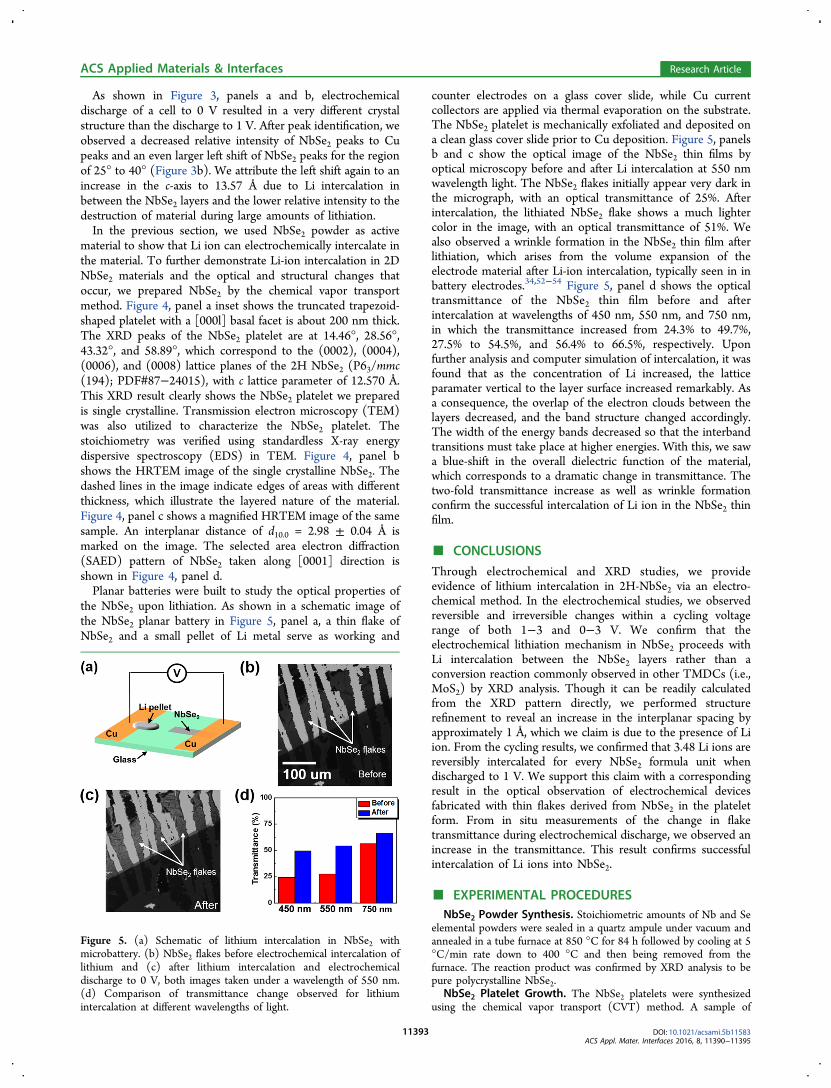
the NbSe2 upon lithiation. As shown in a schematic image ofthe NbSe2 planar battery in Figure 5, panel a, a thin flake ofNbSe2 and a small pellet of Li metal serve as working and
counter electrodes on a glass cover slide, while Cu currentcollectors are applied via thermal evaporation on the substrate.The NbSe2 platelet is mechanically exfoliated and deposited ona clean glass cover slide prior to Cu deposition. Figure 5, panelsb and c show the optical image of the NbSe2 thin films byoptical microscopy before and after Li intercalation at 550 nmwavelength light. The NbSe2 flakes initially appear very dark inthe micrograph, with an optical transmittance of 25%. Afterintercalation, the lithiated NbSe2 flake shows a much lightercolor in the image, with an optical transmittance of 51%. Wealso observed a wrinkle formation in the NbSe2 thin film afterlithiation, which arises from the volume expansion of theelectrode material after Li-ion intercalation, typically seen in inbattery electrodes.34,52−54 Figure 5, panel d shows the opticaltransmittance of the NbSe2 thin film before and afterintercalation at wavelengths of 450 nm, 550 nm, and 750 nm,in which the transmittance increased from 24.3% to 49.7%,27.5% to 54.5%, and 56.4% to 66.5%, respectively. Uponfurther analysis and computer simulation of intercalation, it wasfound that as the concentration of Li increased, the latticeparamater vertical to the layer surface increased remarkably. Asa consequence, the overlap of the electron clouds between thelayers decreased, and the band structure changed accordingly.The width of the energy bands decreased so that the interbandtransitions must take place at higher energies. With this, we sawa blue-shift in the overall dielectric function of the material,which corresponds to a dramatic change in transmittance. Thetwo-fold transmittance increase as well as wrinkle formationconfirm the successful intercalation of Li ion in the NbSe2 thinfilm.
■ CONCLUSIONS
Through electrochemical and XRD studies, we provideevidence of lithium intercalation in 2H-NbSe2 via an electro-chemical method. In the electrochemical studies, we observedreversible and irreversible changes within a cycling voltagerange of both 1−3 and 0−3 V. We confirm that theelectrochemical lithiation mechanism in NbSe2 proceeds withLi intercalation between the NbSe2 layers rather than aconversion reaction commonly observed in other TMDCs (i.e.,MoS2) by XRD analysis. Though it can be readily calculatedfrom the XRD pattern directly, we performed structurerefinement to reveal an increase in the interplanar spacing byapproximately 1 Å, which we claim is due to the presence of Liion. From the cycling results, we confirmed that 3.48 Li ions arereversibly intercalated for every NbSe2 formula unit whendischarged to 1 V. We support this claim with a correspondingresult in the optical observation of electrochemical devicesfabricated with thin flakes derived from NbSe2 in the plateletform. From in situ measurements of the change in flaketransmittance during electrochemical discharge, we observed anincrease in the transmittance. This result confirms successfulintercalation of Li ions into NbSe2.
■ EXPERIMENTAL PROCEDURESNbSe2 Powder Synthesis. Stoichiometric amounts of Nb and Se
elemental powders were sealed in a quartz ampule under vacuum andannealed in a tube furnace at 850 °C for 84 h followed by cooling at 5°C/min rate down to 400 °C and then being removed from thefurnace. The reaction product was confirmed by XRD analysis to bepure polycrystalline NbSe2.
NbSe2 Platelet Growth. The NbSe2 platelets were synthesizedusing the chemical vapor transport (CVT) method. A sample of
Figure 5. (a) Schematic of lithium intercalation in NbSe2 withmicrobattery. (b) NbSe2 flakes before electrochemical intercalation oflithium and (c) after lithium intercalation and electrochemicaldischarge to 0 V, both images taken under a wavelength of 550 nm.(d) Comparison of transmittance change observed for lithiumintercalation at different wavelengths of light.
ACS Applied Materials & Interfaces Research Article
DOI: 10.1021/acsami.5b11583ACS Appl. Mater. Interfaces 2016, 8, 11390−11395
11393
0.9906 g of NbSe2 polycrystalline powder was compressed into a pelletand sealed under vacuum in a quartz ampule with 66.5 mg of iodineadded (equivalent to 4 mg/cm3 of I2 concentration in the ampule),where iodine served as a transport agent in the CVT process. Theampule was heat treated in a horizontal tube furnace at 825 °C for 84h, which resulted in the growth of single-crystalline platelets of NbSe2,confirmed by XRD and TEM.2D-Planar Device Fabrication. For the 2D planar devices, we
used the single crystalline platelet form of NbSe2. After preparing aglass cover slide by sonication in acetone and then methanol, wemounted it to a glass slide with Scotch tape. Via mechanicalexfoliation, we prepared the sample on the glass slide and observedthin flakes of NbSe2 under an optical microscope. The full device wasthen assembled by depositing copper current collectors that wouldform electrical connections between the flake and the rest of thedevice. The device was then finished by constructing a small chamberin which the LiPF6 in EC/DEC (w/w = 1:1) electrolyte could becontained, filling the chamber in argon atmosphere, and sealing thedevice with another slide cover using epoxy glue.Coin Cell Device Fabrication. Coin cells were fabricated using
NbSe2 powder as the active material of the cathode. A slurry mixturewas first prepared with NbSe2 as the main component by addingacetylene black carbon as a conductive additive consistent with otherelectrochemical cell preparation techniques, and polyvinylpyrrolidone(PVP) as a binding agent. The slurry was combined in proportions of7:2:1 NbSe2/acetylene black/PVP by using water as the solvent. Onceall components were evenly combined using a mortar and pestle, themixture was deposited on clean copper foil using the doctor bladecoating method and transferred to a vacuum oven at approximately100 °C to allow the coating to dry completely. After, punches wereused to prepare PVP separator and electrodes for coin cell assembly. Inargon atmosphere, Li metal (Sigma-Aldrich), two sheets of PVPseparator, lithium hexafluorophosphate solution in ethylene carbonateand diethyl carbonate (1 M LiPF6 in EC/DEC w/w = 1:1) electrolyte,and the NbSe2-based electrode were arranged in 20 mm diameter 304stainless steel coin cell cases. The assembly was then crimped atapproximately 1000 psi to form a functional coin cell device.Preparation of NbSe2 Cathodes for XRD Analysis. To perform
XRD on the intercalated NbSe2 coin cell devices, it was first necessaryto remove the NbSe2-containing electrodes from the coin cells. Thistask was made more challenging due to the sensitivity of thecompounds to the atmosphere. We mitigated this concern bydisassembling the coin cells inside a glovebox with argon atmosphere.The samples were mounted for XRD analysis while still inside theglovebox by applying Kapton polyimide film with silicone adhesiveovertop each electrode. We intentionally prevented the tape fromcoming into contact with the sample directly, thus preventingcontamination of the sample while still allowing an inert environmentto be maintained during XRD analysis. XRD analysis was carried outon a D8 Advance with LynxEye and SolX capabilities.Preparation of the NbSe2 Flakes for TEM Analysis. For TEM
investigation, the NbSe2 flake was mounted using epoxy on a Cu TEMgrid with an oval hole. Then, by using the “Scotch tape” method, theflake layers were removed to reduce the thickness to minimum (about15 μm). Final thinning was performed by Ar ions in a precision ionpolishing system (PIPS, Gatan). TEM, EDS, and HRTEM studieswere carried out on 300 kV Titan, FEI electron microscope.
■ AUTHOR INFORMATION
Corresponding Authors*E-mail: [email protected].*E-mail: [email protected].
Author Contributions⊥These authors contributed equally to this work.
NotesThe authors declare no competing financial interest.
■ ACKNOWLEDGMENTSThis work was supported by NSF-CBET Award No. 1335979and internal funding from the National Institute of Standardsand Technology Material Measurement Laboratory. Theauthors thank Irina Kalish from NIST and Christopher Borgfrom UMD for help with the XRD data analysis.
■ REFERENCES(1) Ding, Y.; Wang, Y.; Ni, J.; Shi, L.; Shi, S.; Tang, W. Firstprinciples study of structural, vibrational and electronic properties ofgraphene-like MX2 (MMo, Nb, W, Ta; XS, Se, Te) monolayers.Phys. B 2011, 406, 2254−2260.(2) Schwierz, F. Graphene transistors. Nat. Nanotechnol. 2010, 5,487−496.(3) Avouris, P. Graphene: Electronic and Photonic Properties andDevices. Nano Lett. 2010, 10, 4285−4294.(4) Lee, J.; Lee, S.; Paik, U.; Choi, Y. Aqueous processing of naturalgraphite particulates for lithium-ion battery anodes and theirelectrochemical performance. J. Power Sources 2005, 147, 249−255.(5) Bang, G. S.; Nam, K. W.; Kim, J. Y.; Shin, J.; Choi, J. W.; Choi, S.Effective Liquid-Phase Exfoliation and Sodium Ion Battery Applicationof MoS2 Nanosheets. ACS Appl. Mater. Interfaces 2014, 6, 7084−7089.(6) Bunch, J. S.; Verbridge, S. S.; Alden, J. S.; van der Zande, A. M.;Parpia, J. M.; Craighead, H. G.; McEuen, P. L. Impermeable AtomicMembranes from Graphene Sheets. Nano Lett. 2008, 8, 2458−2462.(7) Lee, C.; Wei, X.; Kysar, J. W.; Hone, J. Measurement of theElastic Properties and Intrinsic Strength of Monolayer Graphene.Science 2008, 321, 385−388.(8) Subrahmanyam, K. S.; Kumar, P.; Maitra, U.; Govindaraj, A.;Hembram, K. P. S. S.; Waghmare, U. V.; Rao, C. N. R. Chemicalstorage of hydrogen in few-layer graphene. Proc. Natl. Acad. Sci. U. S. A.2011, 108, 2674−2677.(9) Stephenson, T.; Li, Z.; Olsen, B.; Mitlin, D. Lithium ion batteryapplications of molybdenum disulfide (MoS2) nanocomposites. EnergyEnviron. Sci. 2014, 7, 209−231.(10) Ayari, A.; Cobas, E.; Ogundadegbe, O.; Fuhrer, M. S. Realizationand electrical characterization of ultrathin crystals of layered transition-metal dichalcogenides. J. Appl. Phys. 2007, 101, 014507.(11) Balandin, A. A.; Ghosh, S.; Bao, W.; Calizo, I.; Teweldebrhan,D.; Miao, F.; Lau, C. N. Superior Thermal Conductivity of Single-Layer Graphene. Nano Lett. 2008, 8, 902−907.(12) Mak, K. F.; He, K.; Shan, J.; Heinz, T. F. Control of valleypolarization in monolayer MoS2 by optical helicity. Nat. Nanotechnol.2012, 7, 494−498.(13) Wang, Q. H.; Kalantar-Zadeh, K.; Kis, A.; Coleman, J. N.;Strano, M. S. Electronics and optoelectronics of two-dimensionaltransition metal dichalcogenides. Nat. Nanotechnol. 2012, 7, 699−712.(14) Tsai, D.; Liu, K.; Lien, D.; Tsai, M.; Kang, C.; Lin, C.; Li, L.; He,J. Few-Layer MoS2 with High Broadband Photogain and Fast OpticalSwitching for Use in Harsh Environments. ACS Nano 2013, 7, 3905−3911.(15) Ozdemir, B.; Barone, V. Structural and electronic properties ofcrystalline graphite-like BC3. Comput. Mater. Sci. 2015, 109, 248−252.(16) O’Neill, A.; Khan, U.; Coleman, J. N. Preparation of HighConcentration Dispersions of Exfoliated MoS2 with Increased FlakeSize. Chem. Mater. 2012, 24, 2414−2421.(17) Novoselov, K. S.; Jiang, D.; Schedin, F.; Booth, T. J.;Khotkevich, V. V.; Morozov, S. V.; Geim, A. K. Two-dimensionalatomic crystals. Proc. Natl. Acad. Sci. U. S. A. 2005, 102, 10451−10453.(18) Zeng, H.; Zhi, C.; Zhang, Z.; Wei, X.; Wang, X.; Guo, W.;Bando, Y.; Golberg, D. White Graphenes”: Boron Nitride Nanorib-bons via Boron Nitride Nanotube Unwrapping. Nano Lett. 2010, 10,5049−5055.(19) Zhang, X.; Zhang, D.; Tang, H.; Ji, X.; Zhang, Y.; Tang, G.; Li,C. Facile synthesis and characterization of hexagonal NbSe2 nano-plates. Mater. Res. Bull. 2014, 53, 96−101.(20) Bonaccorso, F.; Colombo, L.; Yu, G.; Stoller, M.; Tozzini, V.;Ferrari, A. C.; Ruoff, R. S.; Pellegrini, V. Graphene, related two-
ACS Applied Materials & Interfaces Research Article
DOI: 10.1021/acsami.5b11583ACS Appl. Mater. Interfaces 2016, 8, 11390−11395
11394
dimensional crystals, and hybrid systems for energy conversion andstorage. Science 2015, 347, 1246501.(21) Kumagai, N.; Tanno, K.; Nakajima, T.; Watanabe, N. Electrodereaction of niobium chalcogenides as positive electrodes for secondarylithium batteries. J. Electroanal. Chem. Interfacial Electrochem. 1985,184, 87−96.(22) Wang, Y.; Ou, J. Z.; Balendhran, S.; Chrimes, A. F.; Mortazavi,M.; Yao, D. D.; Field, M. R.; Latham, K.; Bansal, V.; Friend, J. R.;Zhuiykov, S.; Medhekar, N. V.; Strano, M. S.; Kalantar-zadeh, K.Electrochemical Control of Photoluminescence in Two-DimensionalMoS2 Nanoflakes. ACS Nano 2013, 7, 10083−10093.(23) Wang, H.; Yuan, H.; Sae Hong, S.; Li, Y.; Cui, Y. Physical andchemical tuning of two-dimensional transition metal dichalcogenides.Chem. Soc. Rev. 2015, 44, 2664−2680.(24) Dresselhaus, M. S.; Dresselhaus, G. Intercalation compounds ofgraphite. Adv. Phys. 2002, 51, 1−186.(25) Chen, K. P.; Chung, F. R.; Wang, M.; Koski, K. J. Dual ElementIntercalation into 2D Layered Bi2Se3 Nanoribbons. J. Am. Chem. Soc.2015, 137, 5431−5437.(26) Yang, H.; Song, T.; Lee, S.; Han, H.; Xia, F.; Devadoss, A.;Sigmund, W.; Paik, U. Tin indium oxide/graphene nanosheetnanocomposite as an anode material for lithium ion batteries withenhanced lithium storage capacity and rate capability. Electrochim. Acta2013, 91, 275−281.(27) Friend, R. H.; Yoffe, A. D. The lithium intercalates of thetransition metal dichalcogenides. Adv. Phys. 1987, 36, 1.(28) Uthaisar, C.; Barone, V.; Fahlman, B. D. On the chemical natureof thermally reduced graphene oxide and its electrochemical Li intakecapacity. Carbon 2013, 61, 558−567.(29) Khrapach, I.; Withers, F.; Bointon, T. H.; Polyushkin, D. K.;Barnes, W. L.; Russo, S.; Craciun, M. F. Novel Highly Conductive andTransparent Graphene-Based Conductors. Adv. Mater. 2012, 24,2844−2849.(30) Wan, J.; Gu, F.; Bao, W.; Dai, J.; Shen, F.; Luo, W.; Han, X.;Urban, D.; Hu, L. Sodium-Ion Intercalated Transparent Conductorswith Printed Reduced Graphene Oxide Networks. Nano Lett. 2015, 15,3763−3769.(31) Su, S.; Hsu, Y.; Chang, Y.; Chiu, M.; Hsu, C.; Hsu, W.; Chang,W.; He, J.; Li, L. Band Gap-Tunable Molybdenum Sulfide SelenideMonolayer Alloy. Small 2014, 10, 2589−2594.(32) Bae, S.; Kim, H.; Lee, Y.; Xu, X.; Park, J.-S.; Zheng, Y.;Balakrishnan, J.; Lei, T.; Ri Kim, H.; Song, Y. I.; Kim, Y.-J.; Kim, K. S.;Ozyilmaz, B.; Ahn, J.-H.; Hong, B. H.; Iijima, S. Roll-to-roll productionof 30-in. graphene films for transparent electrodes. Nat. Nanotechnol.2010, 5, 574−578.(33) Xiong, P.; Peng, L.; Chen, D.; Zhao, Y.; Wang, X.; Yu, G. Two-dimensional nanosheets based Li-ion full batteries with high ratecapability and flexibility. Nano Energy 2015, 12, 816−823.(34) Bao, W.; Wan, J.; Han, X.; Cai, X.; Zhu, H.; Kim, D.; Ma, D.;Xu, Y.; Munday, J. N.; Drew, H. D.; Fuhrer, M. S.; Hu, L. Approachingthe limits of transparency and conductivity in graphitic materialsthrough lithium intercalation. Nat. Commun. 2014, 5, 4224.(35) Wan, J.; Bao, W.; Liu, Y.; Dai, J.; Shen, F.; Zhou, L.; Cai, X.;Urban, D.; Li, Y.; Jungjohann, K.; Fuhrer, M. S.; Hu, L. In SituInvestigations of Li-MoS2 with Planar Batteries. Adv. Energy Mater.2015, 5.10.1002/aenm.201401742(36) Kim, N.; Kim, K. S.; Jung, N.; Brus, L.; Kim, P. Synthesis andElectrical Characterization of Magnetic Bilayer Graphene Intercalate.Nano Lett. 2011, 11, 860−865.(37) Lu, N.; Guo, H.; Wang, L.; Wu, X.; Zeng, X. C. van der Waalstrilayers and superlattices: modification of electronic structures ofMoS2 by intercalation. Nanoscale 2014, 6, 4566−4571.(38) Yu, Y.; Yang, F.; Lu, X. F.; Yan, Y. J.; Cho, Y.-H.; Ma, L.; Niu,X.; Kim, S.; Son, Y.; Feng, D.; Li, S.; Cheong, S.; Chen, X. H.; Zhang,Y. Gate-tunable phase transitions in thin flakes of 1T-TaS2. Nat.Nanotechnol. 2015, 10, 270−276.(39) Wu, H.; Kong, D.; Ruan, Z.; Hsu, P.; Wang, S.; Yu, Z.; Carney,T. J.; Hu, L.; Fan, S.; Cui, Y. A transparent electrode based on a metalnanotrough network. Nat. Nanotechnol. 2013, 8, 421−425.
(40) Li, H.; Pan, W.; Zhang, W.; Huang, S.; Wu, H. TiN Nanofibers:A New Material with High Conductivity and Transmittance forTransparent Conductive Electrodes. Adv. Funct. Mater. 2013, 23, 209−214.(41) Acrivos, J.; Liang, W.; Wilson, J. A.; Yoffe, A. D. Optical studiesof metal-semiconductor transmutations produced by intercalation. J.Phys. C: Solid State Phys. 1971, 4, L18.(42) Mattheiss, L. F. Band Structures of Transition-Metal-Dichalcogenide Layer Compounds. Phys. Rev. B 1973, 8, 3719−3740.(43) Wilson, J. A.; Di Salvo, F. J.; Mahajan, S. Charge-density wavesand superlattices in the metallic layered transition metal dichalcoge-nides. Adv. Phys. 2001, 50, 1171−1248.(44) Castro Neto, A. H. Charge Density Wave, Superconductivity,and Anomalous Metallic Behavior in 2D Transition MetalDichalcogenides. Phys. Rev. Lett. 2001, 86, 4382−4385.(45) Folinsbee, J. T.; Simpson, A. M.; Jericho, M. H. Li diffusion inNbSe2 and Ag0.25NbSe2 single crystals. Mater. Res. Bull. 1986, 21 (8),961−969.(46) Doran, N. J. Electronic Structure and Band Theory ofTransition Metal Dichalcogenides. Physica B+C 1980, 99, 227−237.(47) Cheng, Y.; Nie, A.; Zhang, Q.; Gan, L.; Shahbazian-Yassar, R.;Schwingenschlogl, U. Origin of the Phase Transition in LithiatedMolybdenum Disulfide. ACS Nano 2014, 8, 11447−11453.(48) Nie, A.; Cheng, Y.; Zhu, Y.; Asayesh-Ardakani, H.; Tao, R.;Mashayek, F.; Han, Y.; Schwingenschlogl, U.; Klie, R. F.; Vaddiraju, S.;Shahbazian-Yassar, R. Lithiation-Induced Shuffling of Atomic Stacks.Nano Lett. 2014, 14, 5301−5307.(49) Certain commercial equipment, instruments, or materials areidentified in this paper to specify the experimental procedureadequately. Such identification is not intended to imply recommen-dation or endorsement by the National Institute of Standards andTechnology nor is it intended to imply that the materials or equipmentidentified are necessarily the best available for the purpose.(50) Meerschaut, A.; Deudon, C. Crystal structure studies of the 3R-Nb1.09S2 and the 2H-NbSe2 compounds: correlation between non-stoichiometry and stacking type (= polytypism). Mater. Res. Bull. 2001,36, 1721−1727.(51) Otte, H. M. Lattice Parameter Determinations with an X-RaySpectrogoniometer by the Debye-Scherrer Method and the Effect ofSpecimen Condition. J. Appl. Phys. 1961, 32, 1536−1546.(52) Cui, L.; Hu, L.; Choi, J. W.; Cui, Y. Light-Weight Free-StandingCarbon Nanotube-Silicon Films for Anodes of Lithium Ion Batteries.ACS Nano 2010, 4, 3671−3678.(53) Bao, W.; Miao, F.; Chen, Z.; Zhang, H.; Jang, W.; Dames, C.;Lau, C. N. Controlled ripple texturing of suspended graphene andultrathin graphite membranes. Nat. Nanotechnol. 2009, 4, 562−566.(54) Lacey, S. D.; Wan, J.; Cresce, A. v. W.; Russell, S. M.; Dai, J.;Bao, W.; Xu, K.; Hu, L. Atomic Force Microscopy Studies onMolybdenum Disulfide Flakes as Sodium-Ion Anodes. Nano Lett.2015, 15, 1018−1024.
ACS Applied Materials & Interfaces Research Article
DOI: 10.1021/acsami.5b11583ACS Appl. Mater. Interfaces 2016, 8, 11390−11395
11395