universitÀ degli studi di trieste - arts.units.it · intercalation of alkali metals and gas atoms...
TRANSCRIPT
UNIVERSITÀ DEGLI STUDI DI TRIESTE
XXX CICLO DEL DOTTORATO DI RICERCA IN
_____________________FISICA_______________________
denominazione del dottorato al momento dell’immatricolazione/ name of the doctoral program at the time of enrolment
specify the funding agency, in case they required to be quoted
ELECTRONIC STRUCTURE OF SINGLE AND
FEW LAYERED GRAPHENE STUDIED BY
ANGLE RESOLVED PHOTOEMISSION
SPECTRO-MICROSCOPY
Settore scientifico-disciplinare: _____FIS/03_Fisica della materia_____
DOTTORANDO Ph.D. student
VIKTOR KANDYBA Name - Surname
COORDINATORE Ph.D. program Coordinator
PROF. LIVIO LANCERI Name - Surname
SUPERVISORE DI TESI Thesis Supervisor
PhD. ALEXEI BARINOV Prof. Name - Surname
CO-SUPERVISORE DI TESI Thesis Supervisor
PROF. FULVIO PARMIGIANI Prof. Name - Surname
indicare anche eventuali co-supervisori; nel caso d
i tesi in cotutela, indicare i due direttori di tesi specify also co-supervisors, if any; in case of joint supervision please specify the two thesis directors
ANNO ACCADEMICO 2016/2017
1
Table of Contents
1. Introduction ................................................................................................................................................... 4
2. Experimental considerations.......................................................................................................................... 7
2.1 ARPES and synchrotron radiation ........................................................................................................... 7
2.1.1 Theory and applications of ARPES .................................................................................................. 7
2.1.2 Synchrotron radiation ..................................................................................................................... 17
2.1.3 Advanced methods in photoemission spectroscopy ....................................................................... 21
2.2 Photoemission microscopy at synchrotrons .......................................................................................... 23
2.2.1 Photoemission electron microscopy and low-energy electron microscopy .................................... 23
2.2.2 Micro- and nano-ARPES ................................................................................................................ 25
2.3 SpectroMicroscopy beamline ................................................................................................................ 28
2.3.1 Beamline overview ......................................................................................................................... 28
2.3.2 Energy analyzer .............................................................................................................................. 31
2.3.3 Detector, delay line ......................................................................................................................... 32
2.3.4 Cooling ........................................................................................................................................... 33
2.3.5 Scanning stage, sample localization and identification .................................................................. 33
2.3.6 Data acquisition .............................................................................................................................. 34
2.3.7 Studies of novel materials at SpectroMicroscopy beamline ........................................................... 36
2.3.8 Other micro/nano-ARPES facilities (at ALS, SOLEIL, DIAMOND and SSRF). Advantages and
disadvantages ........................................................................................................................................... 39
2.3.9 Summary and further development ................................................................................................ 41
3. Graphene electronic structure and synthesis ............................................................................................... 42
3.1 Electronic properties of graphene .......................................................................................................... 43
3.2 Bilayer graphene .................................................................................................................................... 46
3.3 Multilayer graphene ............................................................................................................................... 48
3.4 Twisted graphene ................................................................................................................................... 49
3.4.1 Moiré pattern .................................................................................................................................. 49
3.4.2 Van Hove singularities in multilayer graphene .............................................................................. 52
3.4.3 Renormalization of Fermi velocity ................................................................................................. 54
3.4.4 Exotic behavior of quasiparticles in twisted graphene ................................................................... 56
3.5 State of the art: previous ARPES studies of single layer and twisted multilayer graphene. ................. 57
3.6 Alcali metal intercalation and its influence on graphene band structure ............................................... 60
3.7 Growth of graphene on SiC and metal substrates .................................................................................. 62
3.8 Summary and objectives ........................................................................................................................ 65
4. Synthesis of graphene on SiC and study of its electronic properties ........................................................... 66

2
4.1 In situ - Growth of graphene on SiC (0001) and (000-1) and search of suitable twisted nLG sample
system for µ-ARPES measurements ........................................................................................................... 66
4.1.1. Growth protocol and sample holder installation ............................................................................ 66
4.1.2 Morphology and electronic structure of graphene on Si-face of silicon carbide ............................ 68
4.1.3 Morphology and electronic structure of graphene on C-face of silicon carbide ............................. 70
4.2 Electronic structure of multilayer twisted graphene on C-face of SiC .................................................. 72
4.2.1 Pristine graphene. Twisted graphene stacks ................................................................................... 72
4.2.2 Observation of twisted graphene minizone. Odd and even type superlattices ............................... 74
4.2.3 µ-ARPES evidence of interlayer coupling ..................................................................................... 76
4.2.4 Interplay of interlayer couplings in twisted 3LG ............................................................................ 79
4.2.5 4LG graphene ................................................................................................................................. 83
4.2.6 Flat bands areas .............................................................................................................................. 85
4.2.7 Summary of the current chapter and motivation for the further experiments................................. 86
4.3 Electronic structure modification by Li intercalation ............................................................................ 87
4.3.1 Lithium source. Intercalation. Cleaning and oxidation problems: requirements for vacuum
conditions during the measurements. ...................................................................................................... 87
4.3.2 Li intercalation into AA- and AB-stacked graphene ...................................................................... 88
4.3.3 Fermi level shift vs. amount of intercalant ..................................................................................... 91
4.3.4 Initial band structure of two twisted 3LG domains selected for alkali metal atoms intercalation .. 92
4.3.5 Band structure of two twisted 3LG after Li intercalation ............................................................... 96
4.3.6 Observation of double Dirac cones of layers subjected to different twist in Li-doped nLG .......... 97
4.4 Changing electronic structure by K intercalation ................................................................................ 102
4.5 Chapter summary ................................................................................................................................. 104
5. Synthesis of single and bilayer graphene on Ru(0001) and its electronic structure during oxidation and
reduction reactions ......................................................................................................................................... 106
5.1 Sample preparation and graphene growth ........................................................................................... 106
5.2 Electronic structure of graphene on Ru after growth ........................................................................... 108
5.3 Oxygen intercalation under graphene .................................................................................................. 110
5.4 Oxygen de-intercalation by thermal treatment in ultra-high vacuum .................................................. 112
5.5 Oxygen de-intercalation by thermal treatment in H2 atmosphere ........................................................ 113
6. Related works ............................................................................................................................................ 117
7. Summary.................................................................................................................................................... 121
List of abbreviations ...................................................................................................................................... 123
Acknowledgements ....................................................................................................................................... 125
List of publications ........................................................................................................................................ 126
Works Cited ................................................................................................................................................... 127

3
Abstract
This thesis reports the study of electronic band structure of single and few layered graphene grown by
thermal decomposition of SiC at the surface and by C-sublimation on Ru single crystals. Growth
conditions were optimized in order to obtain big few micrometer sized graphene domains. For the first
system twisted multilayer graphene domains were found and chosen for study. On ruthenium only
single layer graphene domains and also the domains with incorporated bilayer patches were obtained
and their electronic properties were investigated after oxidation-reduction reactions at graphene/Ru
interface. The electronic band structure was analyzed using high resolution angle resolved
photoelectron spectroscopy. In order to obtain spectra from individual domains novel
spectromicroscopy end station was used for focusing synchrotron radiation beam to sub-micrometer
spot on the sample surface. Experimental results on twisted graphene confirmed interlayer coupling
and resulting van Hove singularities, graphene Dirac fermions velocity renormalization and other
exotic phenomena predicted by theoretical calculations and partially observed by scanning tunneling
spectroscopy technique. Particular attention has been paid to poorly studied interlayer coupling in
trilayer systems where middle layer has two different couplings being sandwiched between differently
twisted layers. These multilayer graphene domains were also investigated in detail upon alkali metal
intercalation and unexpected splitting of upper part of Dirac cone, related to graphene sublattice
symmetry breaking in the middle graphene layer was found. In graphene on Ru it was first confirmed
that oxidation of Ru under graphene decouples its strongly hybridized π orbitals making graphene p-
doped. Our observations indicate that bilayer patches incorporated into single layer background
remain n-doped and decorated by intercalated oxygen, thereby forming lateral p-n junctions in the
same graphene layer. It was found that hydrogen atmosphere helps to reduce RuOx without the
formation of carbon vacancy defects. However, structural wrinkle patterns appeared due to loss of
original graphene/Ru epitaxial order remain, and in big graphene domains they can trap H2+RuOx
reaction products, making graphene fully decoupled and undoped.
4
1. Introduction
Graphene, a layer of carbon atoms in a honeycomb lattice, captures enormous interest as probably the
most promising component of future electronics thanks to its mechanical robustness, flexibility, and unique
charge carrier quasiparticles propagating like massless high energy Dirac fermions. Although an enormous
number of articles on graphene have been published since the work by A. Geim and K. Novoselov in 2004,
and remarkable progress in fabrication of single devices is achieved, as for example, realization of separately
contacted layers in few layer graphene (nLG), still many questions remain obscured concerning firstly,
graphene’s electronic properties and secondly, efficient ways of graphene mass production growth and
tuning of the properties. Having electron velocities of up to 106 m/s that would allow potential clock rates of
several hundred GHz in graphene based transistors, graphene is a promising material for novel electronics,
and is intensively studied in sense of the exploiting its massless charge carriers and modifying its band
structure into semiconductor-type, with a band gap. The creation of a local band gap in graphene may be
achieved by coupling the π-bands of graphene’s two sublattices, which in the past has been accomplished in
a number of different ways, like hydrogenation, fluorination, removal of carbon atoms, interactions with
various substrates, etc. In graphene bilayer systems it can further be achieved by creation of an interlayer
asymmetry either by surface doping or a perpendicular electric field and, more elegantly, combining the
electrostatic field and breaking graphene sublattice symmetry in external periodic potential, which in a
simplest case can be achieved by rotation of two graphene layers with respect to each other.
If several graphene layers form a stack, the interaction between them is, on the one hand, weak,
allowing realization of various registries between the layers and, on the other hand, strong enough for a wide
range tuning of the electronic properties. For two or more graphene layers that have a mutual rotation, e.g.
twisted multilayer graphene, the band structure depends on the twist angle. For large twist angles the
graphene layers are decoupled in a significant energy window around Dirac point, such that the quasiparticle
dynamics of the twisted layers are essentially similar to single layer graphene, but for smaller angle the
interlayer coupling starts playing important role and leads to Fermi velocity renormalization which is
confirmed by theoretical calculations and appearance of van Hove singularities, observed by scanning
tunneling spectroscopy (STS). At the same time some controversial data on electronic structure of twisted
nLG were reported by ARPES, which need to be clarified. Theoretical works also show that intercalation of
the twist bilayer by alkali and alkaline earth metals leads to the opening of a significant band gap, while
preserving the linear spectrum outside the gap. The present work aims at experimental verification of such
theoretical predictions for graphene electronic structure on such complex structures, which due to their
complexity can be realized only in small size presenting therefore substantial challenge for an
experimentalist. Additionally, we investigate electronic structure of graphene grown on a reactive substrate
that can be used also as a catalyst for gas reactions at the interface between graphene and the substrate.
Specifically, this thesis reports investigation of the electronic structure of single and few-layered
graphene grown by thermal decomposition on SiC and by chemical vapor deposition on Ru and the effects of
intercalation of alkali metals and gas atoms between twisted graphene layers in few layered graphene (on
SiC) and between single and bilayer graphene and catalyst substrate (Ru). Also a simple oxidation-
reductions reaction occurring between graphene and Ru substrate are investigated.
The electronic structure of the above systems is addressed by angle resolved photoemission
spectroscopy, widely used for band mapping of materials. In the work reported here in order to gain
information from individual few micrometer sized domains of graphene a novel synchrotron based scanning
5
photoelectron microscopy technique was mostly used, with which it is possible to map the band structure
from submicrometer spot. Part of results related to graphene on Ru was obtained using LEEM/µ-LEED
instrument.
In the thesis firstly the mainly used technique is described. Theoretical basics of angle resolved
photoemission and synchrotron radiation science are briefly reviewed and then more technical details of
angle resolved photoemission spectromicroscopy technique are given.
Third chapter gives an overview of the graphene science. Since this material boosted a lot of
experimental and theoretical research, its band structure is presented following literature survey. Particular
emphasis is given to interlayer coupling in twisted bi- and multilayer graphene, where initially no coupling
was seen by spatially averaging ARPES, while clearly observed in scanning tunneling spectroscopy. Also the
works on graphene growth are reviewed.
The experimental results of the thesis are presented in chapters 4 and 5, first of which is dedicated to
the electronic structure of multilayer graphene on silicon carbide with particular emphasis on twisted
graphene stacks and their electronic structure tailoring by alkali metal intercalation. The second part is
related to reactive synthesis of graphene on ruthenium and its electronic structure changes during reversible
oxidation/reduction reactions at the interface leading to the change of graphene-to-substrate coupling. Both
systems were grown in situ, which is described in detail in corresponding sections.
The main results of the work are the following:
1. Graphene on SiC
Firstly, graphene was synthesized on two different faces of silicon carbide (Si-terminated and C-
terminated). In the first case we obtained continuous monolayer covering with bilayer islands ontop. Studies
of electronic structure of these islands showed typical for Bernal-stacked graphene double π-band with
parabolic character of dispersion near Dirac point already reported in literature. In case of C-face we
obtained more interesting multilayer graphene flakes with different number of layers and various twist angles
between layers in particular flakes, several of which were studied in details. For large twist angles the
graphene layers showed electronic structure similar to the independent monolayers while for smaller angles
we observed interlayer coupling, which is a controversial question according to different previously reported
ARPES data. Bands interaction results in formation of the non-smooth points in the density of states, so
called van Hove singularities (VHSs), which position with respect to Fermi energy depends on the angle of
rotation between the carbon layers. Set of data obtained experimentally with micro-ARPES has a good
correspondence with the data obtained by other authors using scanning tunneling spectroscopy and
theoretical calculations. For a trilayer graphene which has different twist angles between pairs of top -
middle and middle - bottom layers the velocities differed and the smaller twist angle caused stronger
decrease of charge carrier velocity. In some 3LG we observed the presence of locally flat portions bands as a
consequence of saddle-type van Hove singularity presence, which was also predicted by calculations for
extremely small angles of rotation.
Having confirmed the presence of interlayer coupling in twisted graphene we doped it by alkali
metals in order to investigate if interlayer coupling remains. The intercalation of lithium and potassium was
carried out with further ARPES studies the electronic structure. While potassium does not intercalate
uniformly, Li penetrates into twisted graphene and provides good system to study.
In the thesis the detailed study of the electronic structure of twisted trilayer graphene domains
intercalated by Li is presented. The intercalation caused the increase of interlayer distance and thus the
intensity of the signal from second and third graphene layers became weaker. However, the interlayer
coupling is still present and VHS remains at the same position with respect to Dirac points.
6
An important observation is the appearance of a small band gap in case of doping with lithium,
which for upper layer’s Dirac cone was about (0.08 ± 0.03) eV. This is expected due to symmetry breaking
between graphene sub- lattices. Besides, an unexpected feature observed after Li intercalation, is a
substantial band splitting in the middle layer sandwiched between two different twists: while the π-bands of
top and bottom layers remain as in pristine graphene, the middle layer’s band splits in two, forming two
coaxial Dirac cones with the same intensity and slightly different slopes. We tentatively attribute it to a
Rashba-type symmetry breaking between graphene sub-lattices.
For larger twist angles the observed band splitting is isotropic. If the twist angle between layers is
smaller and van Hove singularities are present in the region of the middle layer’s split band, the splitting is
anisotropic due to the formation of corresponding to VHSs band gaps in both branches.
2. Graphene on Ru(0001) and oxidation-reduction reactions
Second part of the work is dedicated to growth of graphene on Ru(0001) crystal and its turning into
quasi-free-standing graphene with its linear energy dispersion. Electronic structure of single and bilayer
graphene was studied by micro-ARPES and its changes during oxidation and reduction reactions in O2 and
H2 were monitored.
First we confirmed that as-grown graphene layer is strongly coupled to Ru surface and the coupling
could be reduced by oxygen intercalation making the graphene p-doped, while in the bilayer patches the top
layer is decupled after the growth and the charge transfer from the bottom "buffer" layer makes it n-doped.
Then we show that oxygen intercalation does not occur under in the bilayer neither it is efficient in the
regions having high density of bilayer patches. Our results indicate that oxygen atoms decorate bilayer
patches embedded in single layer region thereby producing chemical potential difference within the top
graphene layer, i.e. lateral p-n junction within same graphene plane. The annealing treatment for oxygen de-
intercalation in vacuum destroys the graphene presumably via CO desorption whereas we find that the
annealing in hydrogen helps to de-intercalate oxygen and leave the graphene intact and coupled to ruthenium
as after initial growth. However, after oxygen intercalation the epitaxial relation of graphene on Ru was lost
and LEEM data show the wrinkles, which remain during the process of deintercalation and can trap the
reaction products in certain zones of relatively big graphene flakes. In this case corresponding zones of
graphene remain decoupled and neutrally charged.
7
2. Experimental considerations
2.1 ARPES and synchrotron radiation
2.1.1 Theory and applications of ARPES
Angle-resolved photoemission spectroscopy is the development of photoemission spectroscopy where
emitted from the sample electrons are collected at number of different angles, using hemispherical energy
analyzer with 2D detector and also the rotation of the analyzer or sample itself. ARPES is one of the most
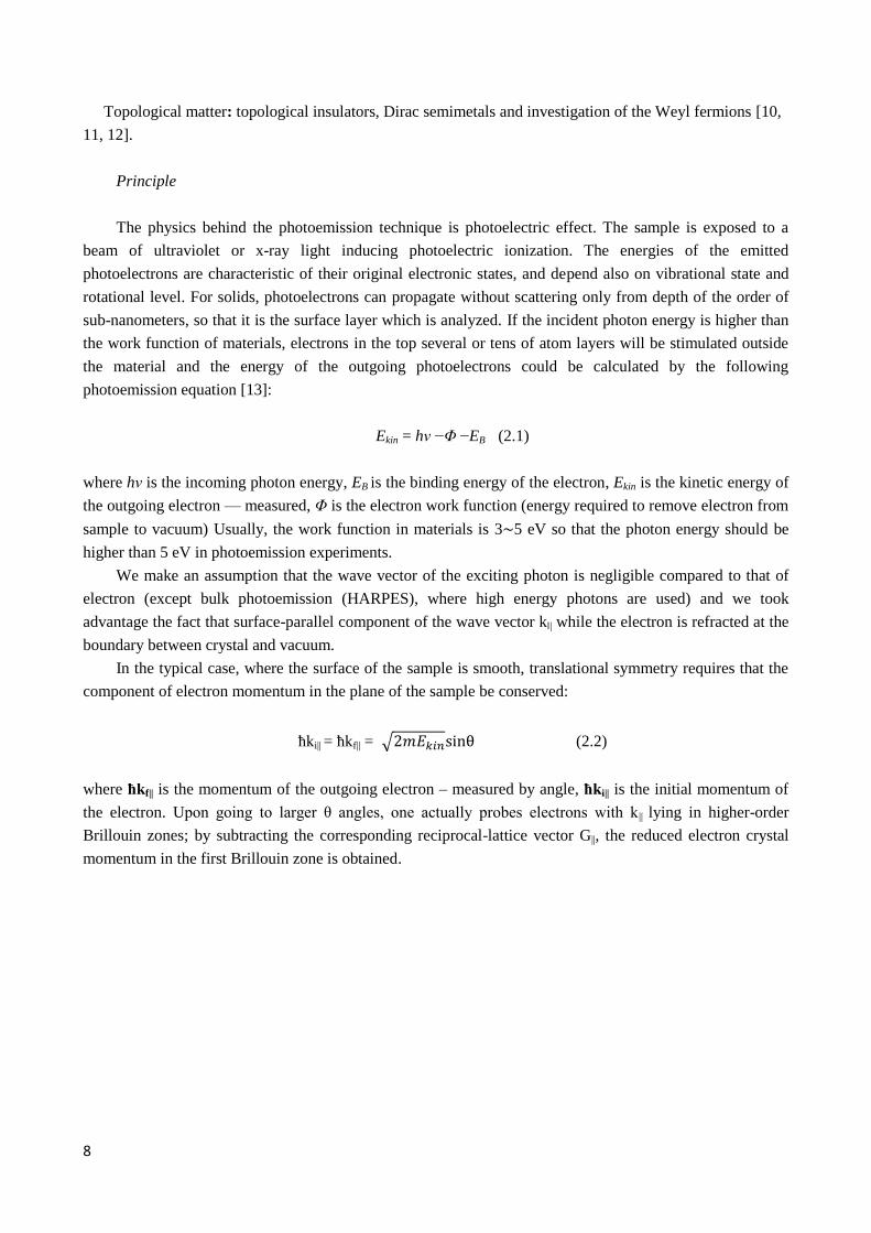
direct methods of studying the electronic structure of solids. By measuring the kinetic energy and angular
distribution of the electrons photoemitted from a sample illuminated with sufficiently high-energy radiation,
one can gain information on both the energy and momentum of the electrons propagating inside a material,
which is necessary for understanding of the connection between electronic, magnetic, and chemical structure
of solids, in particular for those complex systems, which cannot be appropriately described within the
independent-particle picture. [1, 2] It has played a key role in elucidating the properties of many frontier
materials such as the high-temperature superconductors and continues to make a vast impact in correlated
electron physics, surface- and nano-science. [3]
Main merits of ARPES:
- High-resolution information about both energy and momentum;
- Straightforward comparison with theory;
- Direct information about electronic states;
- Sensitive to “many-body” effects;
- Can be applied to small samples.
Limitations:
- Not bulk sensitive in usual energy range (VUV), requires conducting samples, generally probes only
occupied electron states;
- Requires clean crystalline surfaces and UHV. For some types of samples it can be solved by
cleavage in vacuum chamber right before measurements;
- Cannot be applied together with magnetic field or pressure.
As the new techniques and materials are developed some limitations can be overcome. For example
study of bulk becomes possible with the use of bulk photoemission. Also the reactive materials can be
protected by overlaying sheets of non-reactive 2D materials such as boron nitride or graphene, which do not
significantly suppress the useful photoemission signal.
Main present-day applications of ARPES for materials:
Carbon based materials: graphene, molecular electronics (HR-ARPES), BN nanostructure, [4];
2D materials: graphene, dichalcogenides, diselenides
Layered transition metal oxides and high Tc superconductors: quantitative analysis of electron
interactions, Fermi surfaces, renormalisation, energy gaps [5, 6];
Heavy Fermions: ultra-small bandwidth dispersions [7, 8];
Surfaces & interfaces: molecular adsorbates, ultrathin films, stepped surfaces, epitaxially grown nano-
wires [9],
8
Topological matter: topological insulators, Dirac semimetals and investigation of the Weyl fermions [10,
11, 12].
Principle
The physics behind the photoemission technique is photoelectric effect. The sample is exposed to a
beam of ultraviolet or x-ray light inducing photoelectric ionization. The energies of the emitted
photoelectrons are characteristic of their original electronic states, and depend also on vibrational state and
rotational level. For solids, photoelectrons can propagate without scattering only from depth of the order of
sub-nanometers, so that it is the surface layer which is analyzed. If the incident photon energy is higher than
the work function of materials, electrons in the top several or tens of atom layers will be stimulated outside
the material and the energy of the outgoing photoelectrons could be calculated by the following
photoemission equation [13]:
Ekin = hν −Φ −EB (2.1)
where hν is the incoming photon energy, EB is the binding energy of the electron, Ekin is the kinetic energy of
the outgoing electron — measured, Φ is the electron work function (energy required to remove electron from
sample to vacuum) Usually, the work function in materials is 3∼5 eV so that the photon energy should be
higher than 5 eV in photoemission experiments.
We make an assumption that the wave vector of the exciting photon is negligible compared to that of
electron (except bulk photoemission (HARPES), where high energy photons are used) and we took
advantage the fact that surface-parallel component of the wave vector kǁ| while the electron is refracted at the
boundary between crystal and vacuum.
In the typical case, where the surface of the sample is smooth, translational symmetry requires that the
component of electron momentum in the plane of the sample be conserved:
ħki|| = ħkf|| = √2𝑚𝐸𝑘𝑖𝑛sinθ (2.2)
where ħkf|| is the momentum of the outgoing electron – measured by angle, ħki|| is the initial momentum of
the electron. Upon going to larger θ angles, one actually probes electrons with k|| lying in higher-order
Brillouin zones; by subtracting the corresponding reciprocal-lattice vector G||, the reduced electron crystal
momentum in the first Brillouin zone is obtained.
9
Fig 2.1.1 Geometry of angle resolved photoemission measurement
The momentum perpendicular to the sample surface is not conserved because of the broken of
translational symmetry along this direction. The value of 𝑘⊥ can be determined if some a priori assumption
is made for the dispersion of the electron final states involved in the photoemission process; in particular,
one can either use the results of band structure calculations, or adopt a nearly-free-electron description for
the final bulk Bloch states:
𝐸𝑓(𝑘) = ħ2𝑘2
2𝑚− |𝐸0| =
ħ2(𝑘ǁ2+ 𝑘⊥
2 )
2𝑚− |𝐸0| (2.3)
where E0 corresponds to the bottom of the valence band. Here both E0 and Ef are referenced to Fermi energy
Ef and Ekin is referenced to the vacuum level. As Ef = Ekin + Φ and ħ2𝑘2/2𝑚 = 𝐸𝑘𝑖𝑛𝑠𝑖𝑛2𝜃, one can obtain
following value of perpendicular wave vector :
𝑘⊥ =1
ħ√2𝑚(𝐸𝑘𝑖𝑛𝑐𝑜𝑠2𝜃 + 𝑉0) (2.4)
Here V0 = |E0| + Φ is the inner potential, that is equal to energy difference between the bottom of the
valence band E0 and vacuum level Ev
10
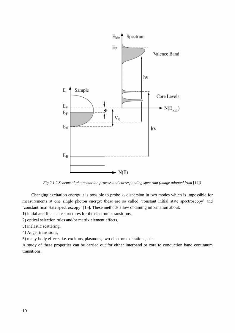
Fig 2.1.2 Scheme of photoemission process and corresponding spectrum (image adopted from [14])
Changing excitation energy it is possible to probe kz dispersion in two modes which is impossible for
measurements at one single photon energy: these are so called ‘constant initial state spectroscopy’ and
‘constant final state spectroscopy’ [15]. These methods allow obtaining information about:
1) initial and final state structures for the electronic transitions,
2) optical selection rules and/or matrix element effects,
3) inelastic scattering,
4) Auger transitions,
5) many-body effects, i.e. excitons, plasmons, two-electron excitations, etc.
A study of these properties can be carried out for either interband or core to conduction band continuum
transitions.
11
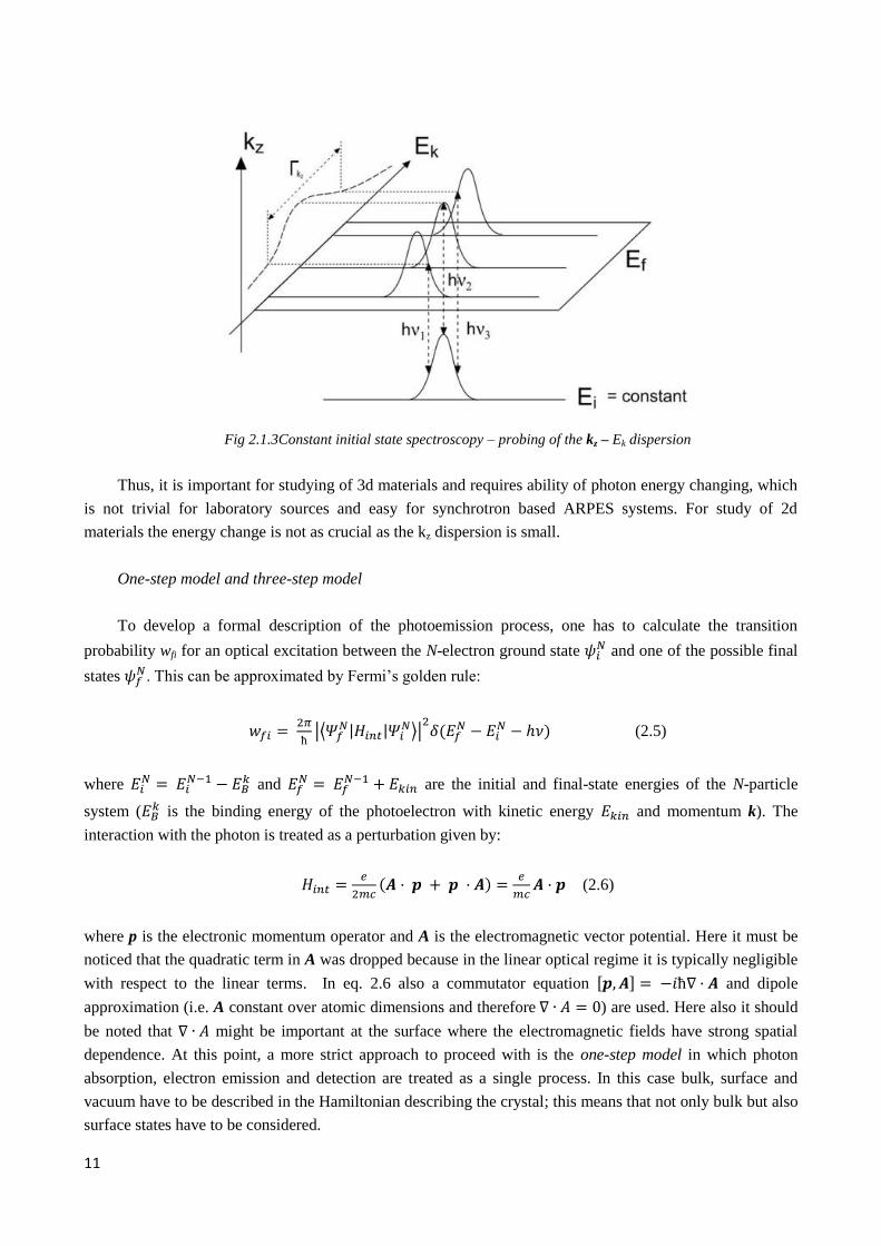
Fig 2.1.3Constant initial state spectroscopy – probing of the kz – Ek dispersion
Thus, it is important for studying of 3d materials and requires ability of photon energy changing, which
is not trivial for laboratory sources and easy for synchrotron based ARPES systems. For study of 2d
materials the energy change is not as crucial as the kz dispersion is small.
One-step model and three-step model
To develop a formal description of the photoemission process, one has to calculate the transition
probability wfi for an optical excitation between the N-electron ground state 𝜓𝑖𝑁 and one of the possible final
states 𝜓𝑓𝑁. This can be approximated by Fermi’s golden rule:
𝑤𝑓𝑖 = 2𝜋
ħ|⟨𝛹𝑓
𝑁|𝐻𝑖𝑛𝑡|𝛹𝑖𝑁⟩|
2𝛿(𝐸𝑓
𝑁 − 𝐸𝑖𝑁 − ℎ𝜈) (2.5)
where 𝐸𝑖𝑁 = 𝐸𝑖
𝑁−1 − 𝐸𝐵𝑘 and 𝐸𝑓
𝑁 = 𝐸𝑓𝑁−1 + 𝐸𝑘𝑖𝑛 are the initial and final-state energies of the N-particle
system (𝐸𝐵𝑘 is the binding energy of the photoelectron with kinetic energy 𝐸𝑘𝑖𝑛 and momentum k). The
interaction with the photon is treated as a perturbation given by:
𝐻𝑖𝑛𝑡 =𝑒
2𝑚𝑐(𝑨 · 𝒑 + 𝒑 · 𝑨) =
𝑒
𝑚𝑐𝑨 · 𝒑 (2.6)
where p is the electronic momentum operator and A is the electromagnetic vector potential. Here it must be
noticed that the quadratic term in A was dropped because in the linear optical regime it is typically negligible
with respect to the linear terms. In eq. 2.6 also a commutator equation [𝒑, 𝑨] = −𝑖ħ∇ · 𝑨 and dipole
approximation (i.e. A constant over atomic dimensions and therefore ∇ ∙ 𝐴 = 0) are used. Here also it should
be noted that ∇ ∙ 𝐴 might be important at the surface where the electromagnetic fields have strong spatial
dependence. At this point, a more strict approach to proceed with is the one-step model in which photon
absorption, electron emission and detection are treated as a single process. In this case bulk, surface and
vacuum have to be described in the Hamiltonian describing the crystal; this means that not only bulk but also
surface states have to be considered.
12
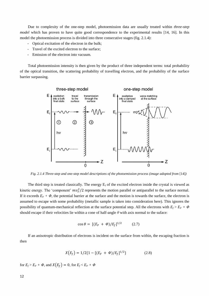
Due to complexity of the one-step model, photoemission data are usually treated within three-step
model which has proven to have quite good correspondence to the experimental results [14, 16]. In this
model the photoemission process is divided into three consecutive stages (fig. 2.1.4):
- Optical excitation of the electron in the bulk;
- Travel of the excited electron to the surface;
- Emission of the electron into vacuum.
Total photoemission intensity is then given by the product of three independent terms: total probability
of the optical transition, the scattering probability of travelling electron, and the probability of the surface
barrier surpassing.
Fig. 2.1.4 Three-step and one-step model descriptions of the photoemission process (image adopted from [14])
The third step is treated classically. The energy Ef of the excited electron inside the crystal is viewed as
kinetic energy. The ‘component’ 𝑚𝑣𝑧2/2 represents the motion parallel or antiparallel to the surface normal.
If it exceeds EF + Φ, the potential barrier at the surface and the motion is towards the surface, the electron is
assumed to escape with some probability (metallic sample is taken into consideration here). This ignores the
possibility of quantum-mechanical reflection at the surface potential step. All the electrons with Ef > EF + Φ
should escape if their velocities lie within a cone of half-angle θ with axis normal to the suface:
cos 𝜃 = [(𝐸𝐹 + 𝛷)/𝐸𝑓]1/2 (2.7)
If an anisotropic distribution of electrons is incident on the surface from within, the escaping fraction is
then
𝑋(𝐸𝑓) = 1/2{1 − [(𝐸𝐹 + 𝛷)/𝐸𝑓]1/2} (2.8)
for Ef > EF + Φ, and 𝑋(𝐸𝑓) = 0, for Ef < EF + Φ
13
The second step can be described in terms of the probability of the scattering, which is described by
“mean free path” parameter λ. It is the average distance that electron passes between two inelastic scattering
events and is determines the escape depth. This value strongly depends on the kinetic energy of electron but
not highly sensitive to the choice of material. Unscattered (primary) electrons are responsible for the sharper
features in the photoemission spectra and carry the information about electronic structure, while inelastically
scattered electrons have lost this information and contribute to the smooth background.
To evaluate first step it would be convenient to factorize the wavefunctions in eq. 2.5 into photoelectron
and (N-1)-electrons terms, which is not trivial because during the photoemission process itself the system
will relax. This evaluation uses so called sudden approximation and is described in details in book by
Hüfner. Finally, the total photoemission intensity measured as a function of Ekin at momentum k is:
𝐼(𝒌, 𝐸𝑘𝑖𝑛) = ∑ 𝑤𝑓,𝑖𝑓,𝑖 and is proportional to:
∑ |𝑀𝑓,𝑖𝑘 |
2𝑓,𝑖 ∑ |𝑐𝑚,𝑖|
2𝛿(𝐸𝑘𝑖𝑛 + 𝐸𝑚
𝑁−1−𝐸𝑖𝑁 − 𝘩𝜈)𝑚 (2.9)
where ⟨𝜙𝑓𝑘|𝐻𝑖𝑛𝑡|𝛹𝑖
𝑘⟩ ≡ 𝑀𝑓,𝑖𝑘 is a is the one-electron matrix element and |𝑐𝑚,𝑖|
2= |⟨𝛹𝑚
𝑁−1|𝛹𝑖𝑁−1⟩|
2 is the
probability that the removal of an electron from the initial state will leave the (N-1)-electron system in the
excited state m.
Here if 𝛹𝑖𝑁−1 = 𝛹𝑚0
𝑁−1 the |𝑐𝑚,𝑖|2will be zero except one particular m = m0, and ARPES spectrum for
one electron will be a sharp peak (delta-function in ideal case). However, in case of correlated system many
|𝑐𝑚,𝑖|2 will be different from zero because the removal of the electron results in change of the effective
potential of the system and thus 𝛹𝑖𝑁−1 will have many non-zero overlaps with eigenstates 𝛹𝑚
𝑁−1.
In many-body physics the correlated electron system is described by Green’s function formalism
G0(r,r’,E). The single particles spectral function is the imaginary part of Green’s function Fourier transform,
G(k, ω),:
𝐴±(𝒌, 𝜔) = ∓1
𝜋Im 𝐺(𝒌, ±𝜔) (2.10)
The Green’s function contains the particles as well as the hole spectra A+ and A
- [2].
The photoemission intensity as a function of energy and momentum of electrons at limited temperature
can be written as
𝐼(𝒌, 𝜔) = 𝐼0(𝒌, 𝝂, 𝑨)𝑓(𝜔)𝐴(𝒌, 𝜔) (2.11)
where k = k|| is the surface parallel momentum of a quasi-two-dimensional system, ω is energy related to
Fermi level, 𝐼0(𝒌, 𝝂, 𝑨) ∼ |𝑀𝑓,𝑖𝑘 |
2 is related to the momentum of electrons, energy and polarization of
impinging photons, and 𝑓(𝜔) = (𝑒𝜔𝐾𝐵𝑇 + 1)−1 is Fermi-Dirac distribution function which determines that
only occupied states could be probed. For the particular case of photoemission the hole Green function for a
quasiparticle can be written as
𝐺(𝒌, 𝜔) =1
𝜔 − ε𝑘 − iГ (2.12)
14
where 1
ħГ = τ−1 is the inverse lifetime of the single-particle state. This form is useful because we can
directly connect the Green function, spectral function and self-energy through Dyson equation [2] and if the
self-energy can be estimated, all the many-body effects can be described by considering a quasi-particle with
the renormalized energy equal to 휀𝑘′ = 휀𝑘 + Σ𝑟(𝒌, 𝜔) + 𝑖Σ𝑖(𝒌, 𝜔), where 휀𝑘 is the energy of bare particle
and the self-energy is Σ(𝒌, 𝜔) = Σ𝑟(𝒌, 𝜔) + 𝑖Σ𝑖(𝒌, 𝜔), where Σ𝑟(𝒌, 𝜔) and Σ𝑖(𝒌, 𝜔) are the real and
imaginary parts, which contain the information about energy renormalization and lifetime of an electron with
band energy εk and momentum k propagating in a many-body system. Finally, the single particle spectral
function can be written as:
𝐴−(𝒌, −𝜔) =1
𝜋
Σ𝑖(𝒌, 𝜔)
[ω − 휀𝑘 − Σ𝑟(𝒌, 𝜔)]2 + [Σ𝑖(𝒌, 𝜔)]2 (2.13)
Thus, if to take into account the interactions, the electrons have to be treated as quasiparticles, it is as
weakly interacting “dressed” particles and this quasiparticle in the state with wave vector k is described by
the spectral function A(k, ω), which for interacting particles is not δ-function anymore but has a finite spread
in energy. The energy distributions of spectral functions for these quasiparticles are described by Lorentzians
and their width determine the quasiparticle lifetimes. In the three-step model of photoemission then the
electron energy bands are broadened and the energy conservation law can be easier fulfilled: instead of δ-
function peaks in the EDCs in angle resolved spectra we will see peaks with finite widths
Instrumentation for ARPES:
Analyzer
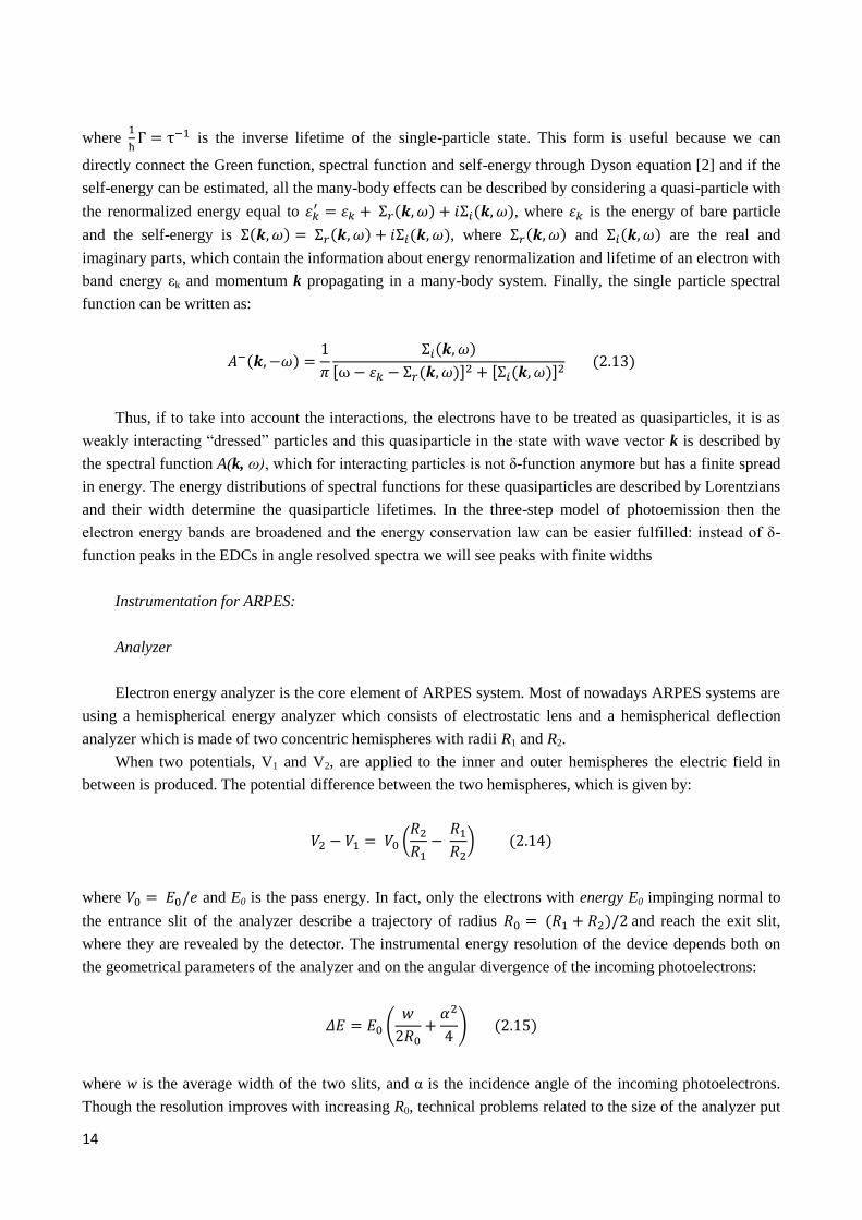
Electron energy analyzer is the core element of ARPES system. Most of nowadays ARPES systems are
using a hemispherical energy analyzer which consists of electrostatic lens and a hemispherical deflection
analyzer which is made of two concentric hemispheres with radii R1 and R2.
When two potentials, V1 and V2, are applied to the inner and outer hemispheres the electric field in
between is produced. The potential difference between the two hemispheres, which is given by:
𝑉2 − 𝑉1 = 𝑉0 (𝑅2
𝑅1−
𝑅1
𝑅2) (2.14)
where 𝑉0 = 𝐸0/𝑒 and E0 is the pass energy. In fact, only the electrons with energy E0 impinging normal to
the entrance slit of the analyzer describe a trajectory of radius 𝑅0 = (𝑅1 + 𝑅2)/2 and reach the exit slit,
where they are revealed by the detector. The instrumental energy resolution of the device depends both on
the geometrical parameters of the analyzer and on the angular divergence of the incoming photoelectrons:
𝛥𝐸 = 𝐸0 (𝑤
2𝑅0+
𝛼2
4) (2.15)
where w is the average width of the two slits, and α is the incidence angle of the incoming photoelectrons.
Though the resolution improves with increasing R0, technical problems related to the size of the analyzer put
15
a limit on the actual value of the radius. Although low pass energy E0 improves the resolution, the electron
transmission probability is reduced at low pass energy, and the signal-to-noise ratio gets worse. Also the
distortions of the electrons trajectories due to residual magnetic fields can affect the quality of the data. The
electrostatic lenses in front of the analyzer have two main purposes: they collect and focus the incoming
photoelectrons into the entrance slit of the analyzer, and they decelerate the electrons to the kinetic energy
E0, in order to increase the resolution and keep it constant. Additionally, modern analyzers’ lens columns are
constructed to convert trajectory of a photoelectron incident at the angle ϑ with respect to the lens column
axis to a position x proportional to ϑ on the entrance slit allowing concomitant measurements of
photoelectrons in both energy and acceptance angle windows using 2D detectors instead of the exit slit (see
Chapter 2.3.2, fig. 2.3.3, b, c).
From general eq. 2.2 we can calculate momentum resolution of the detector:
𝛥𝐾∥ ≃ √2𝑚𝐸𝑘𝑖𝑛/ħ2 · cos 𝜃 · 𝛥𝜃 (2.16)
where Δθ is the angle resolution of the detector.
When acquiring spectra in sweep (or scanning) mode, the voltages of the two hemispheres V1 and V2 -
and hence the pass energy - are held fixed; at the same time, the voltage applied to the electrostatic lenses is
swept in such a way that each channel counts electrons with the selected kinetic energy for the selected
amount of time. In order to reduce the acquisition time per spectrum, the so-called snapshot (or fixed) mode
has been introduced. This mode exploits the relation between the kinetic energy of a photoelectron and its
position inside the detector. If the detector energy range is wide enough, and if the photoemission signal
collected from all the channels is sufficiently strong, the photoemission spectrum can be obtained in one
single shot from the image of the detector.
The acceptance angle depends on the diameter of the lens aperture, the distance from the sample to the
entrance slit, and the lens voltages; as the sample is farther from the opening, the smaller acceptance angle
must be.
Fig. 2.1.5 Electron energy analyzer scheme
16
2D MCP detector
After the electrons travel through the lens and the hemispherical capacitor they are counted by a 2-D
detector. Typically, detector is made up of an electron micro channel plates (MCP) coupled to a phosphorus
screen positioned in front of a charge-couple-device (CCD) camera (several hundred energy channels by
several hundred angular channels). The electron multiplier plate turns a single incident electron into millions
of electrons through secondary emission. This packet of electrons then hits the screen creating a flash of
light. The flashes of light are then detected by CCD camera.
Another type of signal acquisition is based on the delay line which allows detection of the pulse
position by means of the conducting serpentine wire, where the position is determined through the time
difference between pulse arrival on two serpentine terminals. Its advantage is the possibility of time-resolved
experiments, disadvantage is rather big distance between MCP and detector itself and thus image distortions.
This type of detector is used at Spectromicroscopy beamline at Elettra Synchrotron and will be described
further.
Vacuum
The surface of the sample is very sensitive for ARPES experiments, and it’s necessary to keep the
surface clean for a reasonable long time. By simple estimation, in the vacuum with pressure 10−6
torr, a clean
surface will be covered by one layer of atoms in one second. For the conventional light sources like UV, X-
ray guns or lasers the experiment can last several hours or even couple of days that requires vacuum better
than 10-10
torr in order to avoid significant contamination of the sample’s surface. The minimum set consists
of fore-vacuum and turbomolecular pump, for better vacuum it can be supported by ionic and titanium
sublimation pumps. A significant detail which should be taken into account for microscopy end stations is
the issue of vibrations. They are absent for the case of ionic pumps, almost negligible for turbopumps, but
fore-vacuum pumps can cause significant vibrations and need additional efforts for their effect elimination.
Magnetic field
During the photoemission process, the emission angle of photoelectrons carries the momentum
information of electrons in materials. To make sure the path of photoelectrons in the vacuum chamber isn’t
disturbed by any field, it’s necessary to minimize the remnant magnetic field around the path of
photoelectrons. The lower excitation energies are used the higher influence of magnetic field is. To get rid of
these perturbations the mu-metal shields are used made of nickel–iron soft ferromagnetic alloy with very
high permeability, which is used for shielding sensitive electronic equipment against static or low-frequency
magnetic fields.
Light Sources
Modern light sources used in ARPES experiments fall into two main categories:
- laboratory light sources (gas discharge lamps or UV lasers).
Energy resolution of 1 meV and angular resolution of 0.1° [17] can be achieved using a helium
discharge lamp and this performance can be greatly improved when using laser based UV sources - with
17
smaller bandwidths and lower energy. However, standard 6 eV UV laser source allows probing zone
structure only close to Γ-point (central point of Brillouin zone). Also the brilliance of the lab sources is
relatively low and experiments with mapping of wide zone can last up to couple of days.
- synchrotron light sources.
Main advantage of synchrotron light is the wide range of excitation energy and of course its brilliance
which supersedes the lab sources by several orders of magnitude. This allows performing experiments in a
moderate time, which is important for accumulation of signal from low density atomic species in case of
XPS or scanning of wide region in k-space in case of ARPES (this could take days for measurements with
conventional lab source). Other advantage is the improvement of signal-to-noise ratio and decrease of the
adsorbed during experiment species. High flux can be destructive in case of organic samples and some
dimming of the beam could be needed.
The biggest problem in the use of synchrotron light is obviously the cost of its construction and
maintenance, but one synchrotron can provide light to many end stations at once.
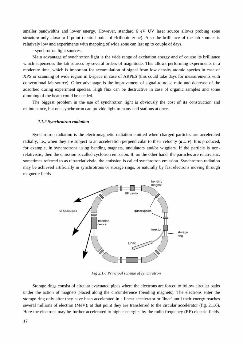
2.1.2 Synchrotron radiation
Synchrotron radiation is the electromagnetic radiation emitted when charged particles are accelerated
radially, i.e., when they are subject to an acceleration perpendicular to their velocity (a v). It is produced,
for example, in synchrotrons using bending magnets, undulators and/or wigglers. If the particle is non-
relativistic, then the emission is called cyclotron emission. If, on the other hand, the particles are relativistic,
sometimes referred to as ultrarelativistic, the emission is called synchrotron emission. Synchrotron radiation
may be achieved artificially in synchrotrons or storage rings, or naturally by fast electrons moving through
magnetic fields.
Fig 2.1.6 Principal scheme of synchrotron
Storage rings consist of circular evacuated pipes where the electrons are forced to follow circular paths
under the action of magnets placed along the circumference (bending magnets). The electrons enter the
storage ring only after they have been accelerated in a linear accelerator or 'linac' until their energy reaches
several millions of electron (MeV); at that point they are transferred to the circular accelerator (fig. 2.1.6).
Here the electrons may be further accelerated to higher energies by the radio frequency (RF) electric fields.
18
When the electrons reach the expected energy they are in a quasi-stationary situation; forced to follow
circular paths by the magnetic field of the bending magnets, they lose, during each turn, part of their energy,
emitting synchrotron radiation. The energy lost in this way is fully regained in passing through the RF
cavities.
Properties of synchrotron radiation:
1. Broad energy range, which covers from microwaves to hard X-rays: users can select the wavelength
required for their experiment;
2. High flux: high intensity photon beam allows rapid experiments or use of weakly scattering crystals;
3. High brilliance: highly collimated photon beam generated by a small divergence and small size
source (spatial coherence);
4. High stability: submicron source stability;
5. Polarization: both linear and circular;
6. Pulsed time structure: pulsed length down to tens of picoseconds allows the resolution of process on
the same time scale.
Bending magnets are present in all circular particle accelerators. The particle passing through a
magnetic field is forced to follow a circular trajectory and emits radiation due to the acceleration. The
radiated power of a charge in a magnetic field can be obtained by the Larmor formula and rapidly increases
with the energy of the circulating particle. The spectrum of the radiation is continuous and is characterized
by a critical energy EC, which divides the spectrum into two parts with equal power [18]. The value of EC
rapidly increases with the energy of the circulating electrons Ɛ and is inversely proportional to the curvature
of the electron trajectory. The angular distribution of the radiation is highly peaked in the forward direction.
The opening angle for photons of critical energy can be approximated with:
1
𝛾 =
𝑚𝑐2
Ɛ (2.17)
The emission cone gets narrower at higher photon energies. Comparison of the brilliance for different
sources is shown on fig. 2.1.7
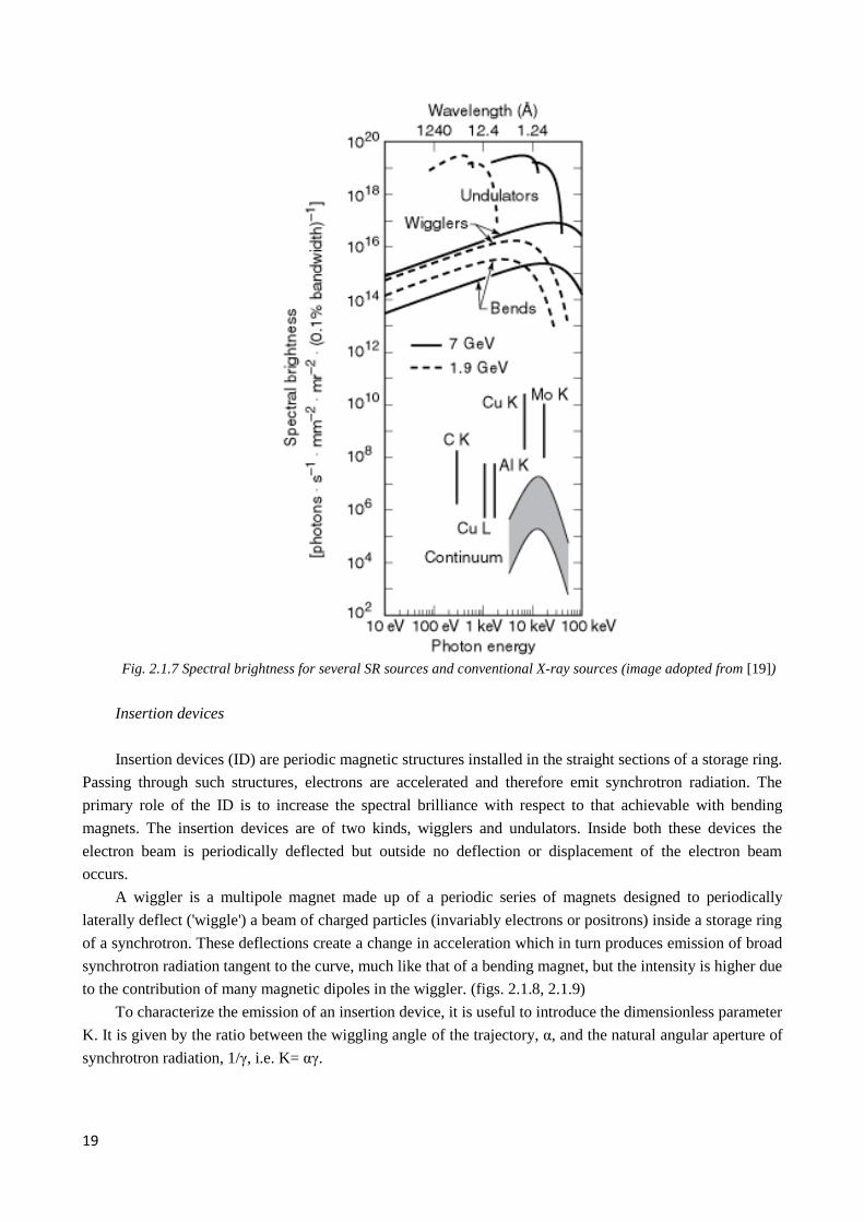
19
Fig. 2.1.7 Spectral brightness for several SR sources and conventional X-ray sources (image adopted from [19])
Insertion devices
Insertion devices (ID) are periodic magnetic structures installed in the straight sections of a storage ring.
Passing through such structures, electrons are accelerated and therefore emit synchrotron radiation. The
primary role of the ID is to increase the spectral brilliance with respect to that achievable with bending
magnets. The insertion devices are of two kinds, wigglers and undulators. Inside both these devices the
electron beam is periodically deflected but outside no deflection or displacement of the electron beam
occurs.
A wiggler is a multipole magnet made up of a periodic series of magnets designed to periodically
laterally deflect ('wiggle') a beam of charged particles (invariably electrons or positrons) inside a storage ring
of a synchrotron. These deflections create a change in acceleration which in turn produces emission of broad
synchrotron radiation tangent to the curve, much like that of a bending magnet, but the intensity is higher due
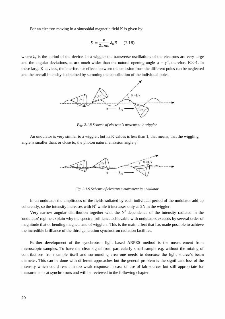
to the contribution of many magnetic dipoles in the wiggler. (figs. 2.1.8, 2.1.9)
To characterize the emission of an insertion device, it is useful to introduce the dimensionless parameter
K. It is given by the ratio between the wiggling angle of the trajectory, α, and the natural angular aperture of
synchrotron radiation, 1/γ, i.e. K= αγ.
20
For an electron moving in a sinusoidal magnetic field K is given by:
𝐾 =𝑒
2𝜋𝑚𝑐𝜆𝑢𝐵 (2.18)
where λu is the period of the device. In a wiggler the transverse oscillations of the electrons are very large
and the angular deviations, α, are much wider than the natural opening angle ψ = γ-1
, therefore K>>1. In
these large K devices, the interference effects between the emission from the different poles can be neglected
and the overall intensity is obtained by summing the contribution of the individual poles.
Fig. 2.1.8 Scheme of electron’s movement in wiggler
An undulator is very similar to a wiggler, but its K values is less than 1, that means, that the wiggling
angle is smaller than, or close to, the photon natural emission angle γ-1
Fig. 2.1.9 Scheme of electron’s movement in undulator
In an undulator the amplitudes of the fields radiated by each individual period of the undulator add up
coherently, so the intensity increases with N2 while it increases only as 2N in the wiggler.
Very narrow angular distribution together with the N2
dependence of the intensity radiated in the
'undulator' regime explain why the spectral brilliance achievable with undulators exceeds by several order of
magnitude that of bending magnets and of wigglers. This is the main effect that has made possible to achieve
the incredible brilliance of the third generation synchrotron radiation facilities.
Further development of the synchrotron light based ARPES method is the measurement from
microscopic samples. To have the clear signal from particularly small sample e.g. without the mixing of
contributions from sample itself and surrounding area one needs to decrease the light source’s beam
diameter. This can be done with different approaches but the general problem is the significant loss of the
intensity which could result in too weak response in case of use of lab sources but still appropriate for
measurements at synchrotrons and will be reviewed in the following chapter.
21
2.1.3 Advanced methods in photoemission spectroscopy
Measuring the unoccupied states
Inverse photoemission spectroscopy (IPES) is a surface science technique used to study the unoccupied
electronic structure of surfaces, thin films, and adsorbates. A well-collimated beam of electrons of a well-
defined energy (< 20 eV) is directed at the sample. These electrons couple to high-lying unoccupied
electronic states and decay to low-lying unoccupied states, and emit the energy difference. The photons
emitted in the decay process are detected and an energy spectrum, photon counts vs. incident electron
energy, is generated. Due to the low energy of the incident electrons, their penetration depth is only a few
atomic layers, making inverse photoemission a particularly surface sensitive technique.
In two-photon photoemission spectroscopy a photon from a pulsed laser excites an electron from a state
below Fermi level to an unoccupied intermediate state below the vacuum level. A second photon of the same
pulse ionizes the intermediate state. The energy distribution of the photoelectrons yields information on the
position and the lifetime of both the initial and, in particular, the intermediate state.
Time-resolved ARPES
Recently developed time-resolved spectroscopy (tr-ARPES) technique is a new tool for the
investigation of elementary scattering processes in such complex materials as quasi-one-dimensional atomic
structures, where, for example, spontaneous periodic lattice modulation can cause a metal-to-insulator
transition at low temperatures. This technique is based on pump-probe scheme, where a femtosecond
infrared laser pulse excites the sample by electron-hole pair creation and a subsequent UV pulse probes the
transient electronic structure after a time delay Δt. This provides access to the observation of scattering
channels in the electronic band structure and associated excited states. Tr-ARPES main subjects of research
are ultrafast changes of the occupied electronic structure including metal-to-insulator transitions, transient
populations in the unoccupied part of the band structure, cooling of excited carriers due electron-phonon
coupling, collective excitation modes such as coherent phonons, relaxation rate of electron quasiparticles in
high-temperature cuprates [20, 21, 22, 23] superconductors and graphene [24, 25] .
Spin-resolved ARPES
Electron spin determines magnetic properties and can control how charged currents flow. The latest
trend in materials science, topological insulators (TIs), is an extreme example. They are insulators in bulk but
good conductors on the surface – where the electron spin and momentum of fast-moving surface electrons
are locked together. In a spin-resolved ARPES experiment, an electrostatic energy analyzer provides an
energy and momentum selected photoelectron beam at the exit aperture while preserving the spin
polarization and spin orientation. Rather inefficient spin detection schemes that are based on spin-dependent
scattering processes need to be applied in order to determine the spin polarization. Among these, Mott
scattering and polarized low-energy electron diffraction (PLEED) are the most frequently used. In Mott
detectors the high-energy electrons penetrate the target foil of several hundred nanometers thickness, which
usually consists of Au or some other heavy element providing a strong spin-orbit interaction. These devices
can thus be operated over weeks and months under stable conditions. PLEED detectors are more efficient in
terms final intensity but less stable due to high demand to the quality of detector’s surface thus they need
frequent calibrations. Two detectors placed symmetrically with respect to the beam axis measure the left-
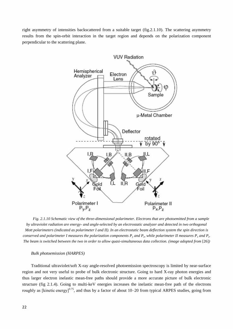
22
right asymmetry of intensities backscattered from a suitable target (fig.2.1.10). The scattering asymmetry
results from the spin-orbit interaction in the target region and depends on the polarization component
perpendicular to the scattering plane.
Fig. 2.1.10 Schematic view of the three-dimensional polarimeter. Electrons that are photoemitted from a sample
by ultraviolet radiation are energy- and angle-selected by an electrostatic analyzer and detected in two orthogonal
Mott polarimeters (indicated as polarimeter I and II). In an electrostatic beam deflection system the spin direction is
conserved and polarimeter I measures the polarization components Py and Pz, while polarimeter II measures Px and Pz.
The beam is switched between the two in order to allow quasi-simultaneous data collection. (image adopted from [26])
Bulk photoemission (HARPES)
Traditional ultraviolet/soft X-ray angle-resolved photoemission spectroscopy is limited by near-surface
region and not very useful to probe of bulk electronic structure. Going to hard X-ray photon energies and
thus larger electron inelastic mean-free paths should provide a more accurate picture of bulk electronic
structure (fig 2.1.4). Going to multi-keV energies increases the inelastic mean-free path of the electrons
roughly as [kinetic energy]0.75
, and thus by a factor of about 10–20 from typical ARPES studies, going from
23
about 5 Å to about 50–100 Å, thereby markedly enhancing the bulk sensitivity of the measurement, and also
in principle permitting the study layers deep beneath the surface [27].
As the photon energy and momentum is much larger than in UPS, this must be included in the simplest
form of the wave vector conservation equation:
𝑘𝑖 = [𝑘𝑓 − 𝑘ℎ𝜈] − 𝑔ℎ𝑘𝑙 (2.19)
where 𝑘ℎ𝜈 is the wave vector of the photon and 𝑔ℎ𝑘𝑙 is the magnitude of the bulk reciprocal lattice vector
involved in the direct transitionsat a given photon energy. As in all ARPES measurements, the relative
intensities of various features will depend on the specific matrix elements involved, with these in turn
depending roughly on the weighted atomic cross-sections contributing to each band, as well as on the overall
symmetry of the experimental geometry. Cross-section values will cause that d- and f -bands will be strongly
suppressed as the energy is increased, while s- and p-bands will gain in importance. [28, 29] Although the
latter are more important in general with respect to transport properties, learning something about d- and f-
thus has to be more indirect, through d- and f -hybridization with s- and p-states [14].
2.2 Photoemission microscopy at synchrotrons
Heaving briefly discussed the above advanced photoemission methods we follow with more detailed
description of the application of photoemission in microscopy. Since photoemission spectromicroscopy
techniques require high photon flux, these are exploited exclusively at synchrotrons. Conventional
synchrotron ARPES end stations usually have beam spot size about 1 mm2
which can be not suitable for
acquisition from some micro- or nanostructured objects, for example semiconductor device prototypes. For a
polycrystalline sample the surface consists of thousand domains which can have different orientation or even
different tilt with respect to the sample holder. In this case a broad beam covering numerous domains at once
will give a mixed signal containing miscellaneous contributions. This will result in broadening of the bands
or poor useful signal to substrate signal ratio in better case, or totally mixed picture without any possibility to
distinguish particular features in the worst case. Two approaches are used to subtract photoemission data
from small areas of interest: 1) photoelectron emission microscopy (PEEM), where photoelectrons are
projected on the detector preserving their original position on the surface; 2) scanning photoemission
microscopy, where incident photon beam is focused to a small spot.
2.2.1 Photoemission electron microscopy and low-energy electron microscopy
Photoemission electron microscopy (PEEM) is a widely used type of emission microscopy. PEEM
utilizes local variations in electron emission to generate image contrast. The excitation is usually produced
by UV light, synchrotron radiation or X-ray sources. PEEM measures the coefficient indirectly by collecting
the emitted secondary electrons generated in the electron cascade that follows the creation of the primary
core hole in the absorption process. The cathode lens, or immersion objective lens, is used to image electrons
emitted from surfaces [30, 31]. In a microscope that uses this type of objective, the sample surface acts as the
cathode held at a negative potential, whereas the anode (objective lens) has a central aperture to allow for the
passage of the emitted electrons towards the imaging column. PEEM is limited in resolution by chromatic
and spherical aberrations of the electron lenses. It was shown that aberration correction can improve the
resolution down to 1 nm.
24
An energy filter can be added to the instrument in order to select the electrons that will contribute to the
image. This option is particularly used for analytical applications of the PEEM. By using an energy filter, a
PEEM microscope can be seen as imaging UPS or XPS. By using this method, spatially resolved
photoemission spectra can be acquired with spatial resolutions on the 100 nm scale and with sub-eV
resolution. Using such instrument, one can acquire elemental images with chemical state sensibility or work
function maps. Also, since the photoelectrons are emitted only at the very surface of the material, surface
termination maps can be acquired. Angle resolved photoemission data also can be taken, however, energy
and momentum resolution of the obtained data are typically of the order of 200 meV and 0.05 Å-1
.
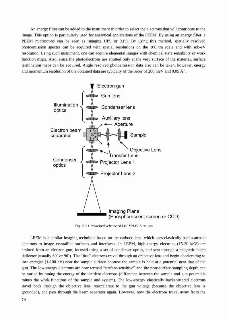
Fig. 2.2.1 Principal scheme of LEEM/LEED set-up
LEEM is a similar imaging technique based on the cathode lens, which uses elastically backscattered
electrons to image crystalline surfaces and interfaces. In LEEM, high-energy electrons (15-20 keV) are
emitted from an electron gun, focused using a set of condenser optics, and sent through a magnetic beam
deflector (usually 60˚ or 90˚). The “fast” electrons travel through an objective lens and begin decelerating to
low energies (1-100 eV) near the sample surface because the sample is held at a potential near that of the
gun. The low-energy electrons are now termed “surface-sensitive” and the near-surface sampling depth can
be varied by tuning the energy of the incident electrons (difference between the sample and gun potentials
minus the work functions of the sample and system). The low-energy elastically backscattered electrons
travel back through the objective lens, reaccelerate to the gun voltage (because the objective lens is
grounded), and pass through the beam separator again. However, now the electrons travel away from the
25
condenser optics and into the projector lenses. Imaging of the back focal plane of the objective lens into the
object plane of the projector lens (using an intermediate lens) produces a diffraction pattern (low-energy
electron diffraction, LEED) at the imaging plane and recorded in a number of different ways. The intensity
distribution of the diffraction pattern will depend on the periodicity at the sample surface and is a direct
result of the wave nature of the electrons. One can produce individual images of the diffraction pattern spot
intensities by turning off the intermediate lens and inserting a contrast aperture in the back focal plane of the
objective lens (or, in state-of-the-art instruments, in the center of the separator, as chosen by the excitation of
the objective lens), thus allowing for real-time observations of dynamic processes at surfaces.
2.2.2 Micro- and nano-ARPES
Focusing down the beam to the size smaller than the explored features and careful positioning of the
sample would allow obtaining clear signal from the desired area of interest. Such demagnification can be
done by Schwarzschild objectives (SO) or Fresnel zone plates (FZP). Moveable stage will allow mapping
and finding the right region and rotating energy analyzer or sample stage is needed for taking of angle-
resolved data. Another solution can be a wide acceptance angle or combined installation. More extreme way
of realization is the rotation of the whole chamber that would allow to use fixed with respect to the chamber
huge analyzer and thus more efficient energy analyzer. This kind of end stations with particular emphasis on
the SpectroMicroscopy beamline, where the experiments described in the thesis were preformed, will be
discussed in the next chapter.
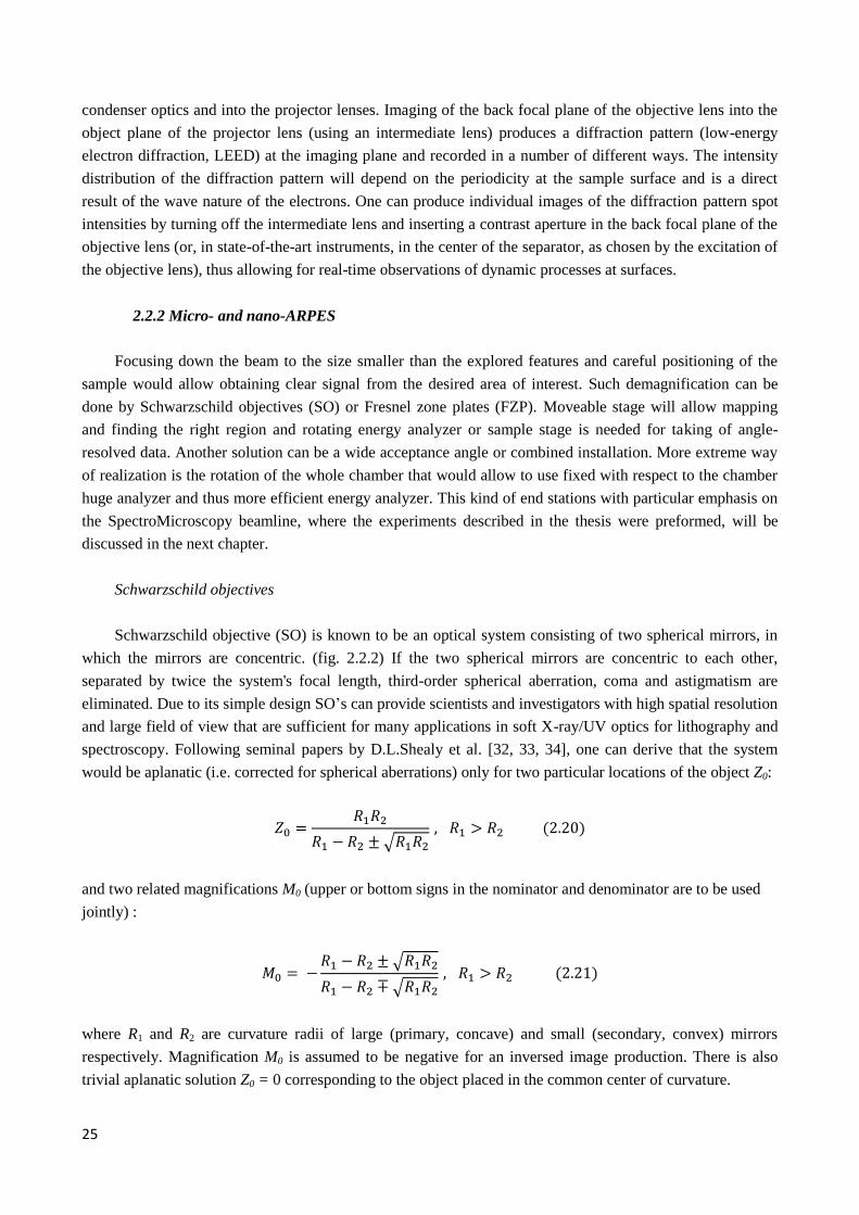
Schwarzschild objectives
Schwarzschild objective (SO) is known to be an optical system consisting of two spherical mirrors, in
which the mirrors are concentric. (fig. 2.2.2) If the two spherical mirrors are concentric to each other,
separated by twice the system's focal length, third-order spherical aberration, coma and astigmatism are
eliminated. Due to its simple design SO’s can provide scientists and investigators with high spatial resolution
and large field of view that are sufficient for many applications in soft X-ray/UV optics for lithography and
spectroscopy. Following seminal papers by D.L.Shealy et al. [32, 33, 34], one can derive that the system
would be aplanatic (i.e. corrected for spherical aberrations) only for two particular locations of the object Z0:
𝑍0 =𝑅1𝑅2
𝑅1 − 𝑅2 ± √𝑅1𝑅2
, 𝑅1 > 𝑅2 (2.20)
and two related magnifications M0 (upper or bottom signs in the nominator and denominator are to be used
jointly) :
𝑀0 = −𝑅1 − 𝑅2 ± √𝑅1𝑅2
𝑅1 − 𝑅2 ∓ √𝑅1𝑅2
, 𝑅1 > 𝑅2 (2.21)
where R1 and R2 are curvature radii of large (primary, concave) and small (secondary, convex) mirrors
respectively. Magnification M0 is assumed to be negative for an inversed image production. There is also
trivial aplanatic solution Z0 = 0 corresponding to the object placed in the common center of curvature.
26
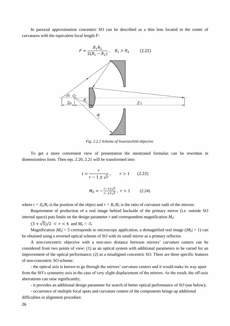
In paraxial approximation concentric SO can be described as a thin lens located in the center of
curvatures with the equivalent focal length F:
𝐹 =𝑅1𝑅2
2(𝑅1 − 𝑅2) , 𝑅1 > 𝑅2 (2.22)
Fig. 2.2.2 Scheme of Swartzschild objective
To get a more convenient view of presentation the mentioned formulas can be rewritten in
dimensionless form. Then eqs. 2.20, 2.21 will be transformed into:
𝑡 =𝑟
𝑟 − 1 ± √𝑟 , 𝑟 > 1 (2.23)
𝑀0 = −𝑟−1±√𝑟
𝑟−1∓√𝑟 , 𝑟 > 1 (2.24)
where t = Z0/R2 is the position of the object and r = R1/R2 is the ratio of curvature radii of the mirrors.
Requirement of production of a real image behind backside of the primary mirror (i.e. outside SO
internal space) puts limits on the design parameter r and correspondent magnification M0:
(3 + √5)/2 < 𝑟 < 4 and M0 < -5.
Magnification |M0| > 5 corresponds to microscopy application, a demagnified real image (|M0| < 1) can
be obtained using a reverted optical scheme of SO with its small mirror as a primary reflector.
A non-concentric objective with a non-zero distance between mirrors’ curvature centers can be
considered from two points of view: (1) as an optical system with additional parameters to be varied for an
improvement of the optical performance; (2) as a misaligned concentric SO. There are three specific features
of non-concentric SO scheme:
- the optical axis is known to go through the mirrors’ curvature centers and it would make its way apart
from the SO’s symmetry axis in the case of very slight displacement of the mirrors. As the result, the off-axis
aberrations can raise significantly;
- it provides an additional design parameter for search of better optical performance of SO (see below);
- occurrence of multiple focal spots and curvature centers of the components brings up additional
difficulties in alignment procedure.
27
For nonconcentric SO the magnification M for arbitrary position of object Z0 is:
𝑀 =𝑓1𝑓2
𝑓12 + 𝐿(𝑍0 + 𝑓1)
(2.25)
where 𝑓1 and 𝑓2 are the focal lengths of the large and small mirrors respectively and L is the distance
between main planes o the mirrors.
Calculations by Artioukov et al. [35] show that for relatively small longitudinal (along the optical axis)
displacement of the mirror’s curvature centers the optical performance of SO has been proven to remain
close to that of concentric scheme. Change of the mirrors’ position for several hundred microns can be easily
compensated by tuning the object – image distance without any observable degradation of the spatial
resolution.
The objective can be aligned by performing the Foucault test UV light and MCP detector. In such a test,
a knife edge is scanned perpendicular to the beam through the focus, while observing the shadow projected
by the knife edge on a screen placed behind it [36]. The shadow exhibits characteristic patterns
(foucaultgrams) which indicate the dominating aberration and therefore which of the objective’s parameter
(pitch, yaw or gap) has to be adjusted, and in which direction. This process is iterative: once the correction is
done, more precise focusing and next foucaultgram goes on until the physical limit defined by high order
optical aberrations is reached.
One limit of SO-like reflective optical systems is relatively low magnification/demagnification ratio as
the result of its centimeter-scale focal length and extremely long object-image distance needed for high
magnification imaging. The main limit however is determined by the fact that SO optics is normal incidence
optics and multilayer coating of SO mirrors is needed to efficiently reflect photons with energies above 20
eV. With such multilayers the reflectivity of the mirror for selected energy line can be increased to ~50%,
obviously sacrificing the wavelength tunability of SO.
Fresnel zone plates based focusing
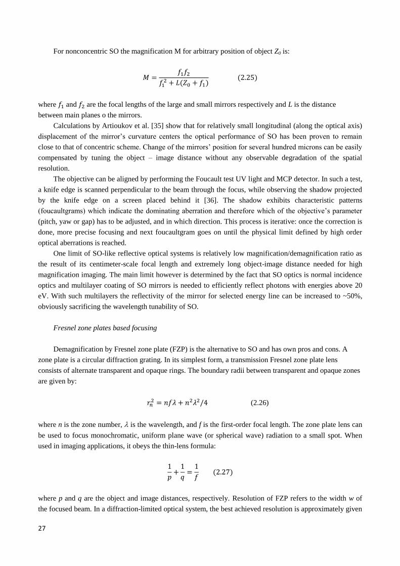
Demagnification by Fresnel zone plate (FZP) is the alternative to SO and has own pros and cons. A
zone plate is a circular diffraction grating. In its simplest form, a transmission Fresnel zone plate lens
consists of alternate transparent and opaque rings. The boundary radii between transparent and opaque zones
are given by:
𝑟𝑛2 = 𝑛𝑓𝜆 + 𝑛2𝜆2/4 (2.26)
where n is the zone number, is the wavelength, and f is the first-order focal length. The zone plate lens can
be used to focus monochromatic, uniform plane wave (or spherical wave) radiation to a small spot. When
used in imaging applications, it obeys the thin-lens formula:
1
𝑝+
1
𝑞=
1
𝑓 (2.27)
where p and q are the object and image distances, respectively. Resolution of FZP refers to the width w of
the focused beam. In a diffraction-limited optical system, the best achieved resolution is approximately given
28
by 𝑤 =𝜆
2𝑁𝐴 where NA is the numerical aperture of the system, defined as the sine of the half angle of the
cone of light that leaves the zone plate. For a given wavelength λ and focal length f, increasing resolution
translates to increasing the NA of the system, and thus, increasing the number of zones. As the zone number
n gets larger, the width of the nth zone gets smaller. The thinnest zone width is the N
th zone (the outermost
zone on the zone plate) and tends to be the most difficult zone to fabricate lithographically. It is therefore is
useful to relate the resolution of the zone plate w to the number of zones N and width of the outer-most zone
Δr. To avoid chromatic blurring, the number of zones, N, must be less than the inverse relative spectral
bandwidth, /.
Fig. 2.2.3 Fresnel zone plate
The main disadvantage of FZP’s use is significant loss of the brilliance, however they provide
submicron beam width as output and also the same zone plate will focus light of many wavelengths (to
different foci) and can be effectively used for UV/X-Ray microscopy at synchrotrons, where wide range of
wavelength are provided. Recently 12 nm resolution was reported for soft X-ray microscope with FZP. [37]
2.3 SpectroMicroscopy beamline
2.3.1 Beamline overview
SpectroMicroscopy beamline is the realization of ARPES for a small, submicron spot including a
possibility of photoemission imaging of a sample surface, scanning the sample’s surface line by line. This is
achieved by focusing of UV beam down to submicron size by means of Schwarzschild objectives and use of
moveable electron energy analyzer and sample scanning stage (Figure 2.3.1, a). Angle resolved data are
taken at fixed position of the sample and with rotation of the analyzer around the stage. Modes of operation
will be reviewed further.
Beamline 3.2R (SpectroMicroscopy) uses the U12.5 undulator in ELETTRA storage ring in the section
3.2. Undulator’s main parameters at 2.0 GeV/400 mA operation are the following:
29
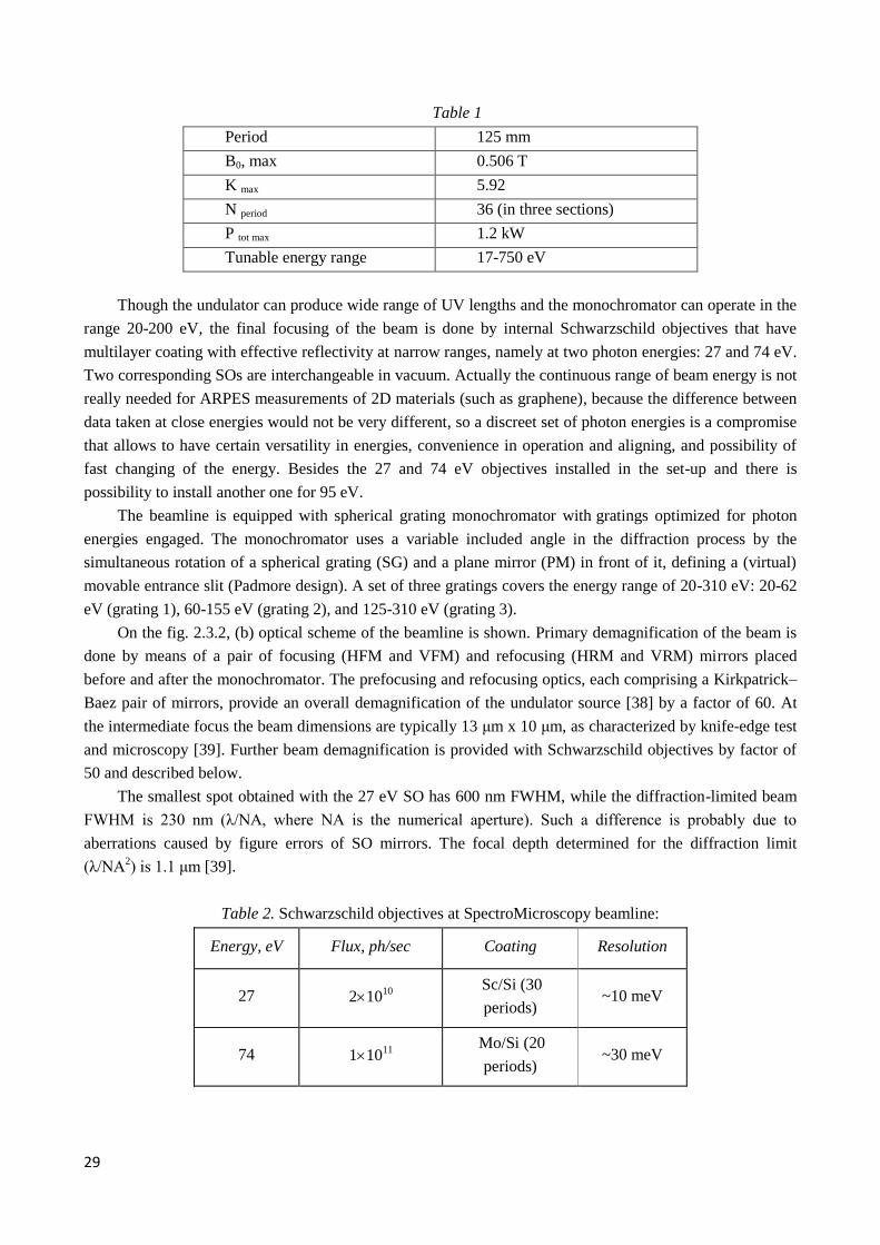
Table 1
Period 125 mm
B0, max 0.506 T
K max 5.92
N period 36 (in three sections)
P tot max 1.2 kW
Tunable energy range 17-750 eV
Though the undulator can produce wide range of UV lengths and the monochromator can operate in the
range 20-200 eV, the final focusing of the beam is done by internal Schwarzschild objectives that have
multilayer coating with effective reflectivity at narrow ranges, namely at two photon energies: 27 and 74 eV.
Two corresponding SOs are interchangeable in vacuum. Actually the continuous range of beam energy is not
really needed for ARPES measurements of 2D materials (such as graphene), because the difference between
data taken at close energies would not be very different, so a discreet set of photon energies is a compromise
that allows to have certain versatility in energies, convenience in operation and aligning, and possibility of
fast changing of the energy. Besides the 27 and 74 eV objectives installed in the set-up and there is
possibility to install another one for 95 eV.
The beamline is equipped with spherical grating monochromator with gratings optimized for photon
energies engaged. The monochromator uses a variable included angle in the diffraction process by the
simultaneous rotation of a spherical grating (SG) and a plane mirror (PM) in front of it, defining a (virtual)
movable entrance slit (Padmore design). A set of three gratings covers the energy range of 20-310 eV: 20-62
eV (grating 1), 60-155 eV (grating 2), and 125-310 eV (grating 3).
On the fig. 2.3.2, (b) optical scheme of the beamline is shown. Primary demagnification of the beam is
done by means of a pair of focusing (HFM and VFM) and refocusing (HRM and VRM) mirrors placed
before and after the monochromator. The prefocusing and refocusing optics, each comprising a Kirkpatrick–
Baez pair of mirrors, provide an overall demagnification of the undulator source [38] by a factor of 60. At
the intermediate focus the beam dimensions are typically 13 μm x 10 μm, as characterized by knife-edge test
and microscopy [39]. Further beam demagnification is provided with Schwarzschild objectives by factor of
50 and described below.
The smallest spot obtained with the 27 eV SO has 600 nm FWHM, while the diffraction-limited beam
FWHM is 230 nm (λ/NA, where NA is the numerical aperture). Such a difference is probably due to
aberrations caused by figure errors of SO mirrors. The focal depth determined for the diffraction limit
(λ/NA2) is 1.1 μm [39].
Table 2. Schwarzschild objectives at SpectroMicroscopy beamline:
Energy, eV Flux, ph/sec Coating Resolution
27 21010
Sc/Si (30
periods) ~10 meV
74 11011
Mo/Si (20
periods) ~30 meV

30
Fig. 2.3.1 a) General measurement scheme, b) Beamline design (image adopted from [36])
At SpectroMicroscopy beamline SO’s are used in both this ways: demagnification of the UV beam for
photoemission microscopy and magnification of the sample for observation in the optical microscope (fig.
2.3.2).
Fig. 2.3.2 Optical imaging for quick search of the area of interest. a) scheme; b) real view; c) example of sample
observation in the optical microscope – graphene flakes on SiC can be seen FOV=200µm.
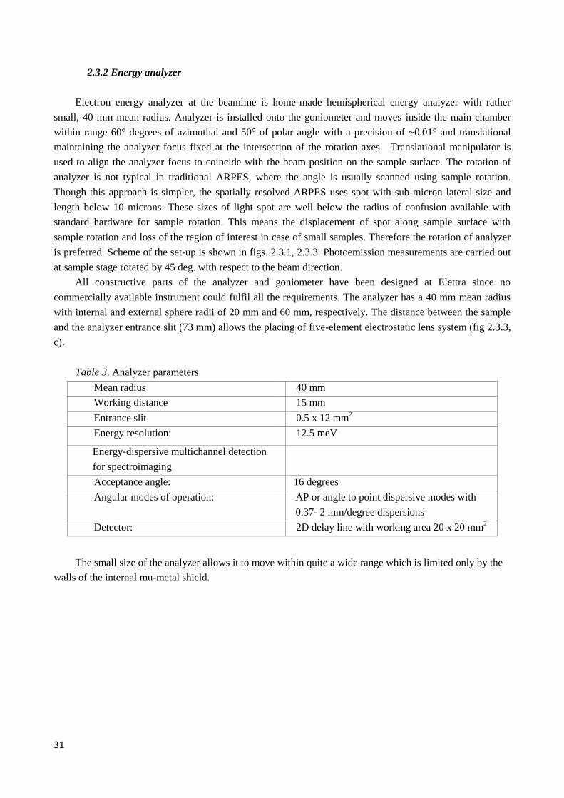
31
2.3.2 Energy analyzer
Electron energy analyzer at the beamline is home-made hemispherical energy analyzer with rather
small, 40 mm mean radius. Analyzer is installed onto the goniometer and moves inside the main chamber
within range 60° degrees of azimuthal and 50° of polar angle with a precision of ~0.01° and translational
maintaining the analyzer focus fixed at the intersection of the rotation axes. Translational manipulator is
used to align the analyzer focus to coincide with the beam position on the sample surface. The rotation of
analyzer is not typical in traditional ARPES, where the angle is usually scanned using sample rotation.
Though this approach is simpler, the spatially resolved ARPES uses spot with sub-micron lateral size and
length below 10 microns. These sizes of light spot are well below the radius of confusion available with
standard hardware for sample rotation. This means the displacement of spot along sample surface with
sample rotation and loss of the region of interest in case of small samples. Therefore the rotation of analyzer
is preferred. Scheme of the set-up is shown in figs. 2.3.1, 2.3.3. Photoemission measurements are carried out
at sample stage rotated by 45 deg. with respect to the beam direction.
All constructive parts of the analyzer and goniometer have been designed at Elettra since no
commercially available instrument could fulfil all the requirements. The analyzer has a 40 mm mean radius
with internal and external sphere radii of 20 mm and 60 mm, respectively. The distance between the sample
and the analyzer entrance slit (73 mm) allows the placing of five-element electrostatic lens system (fig 2.3.3,
c).
Table 3. Analyzer parameters
Mean radius 40 mm
Working distance 15 mm
Entrance slit 0.5 x 12 mm2
Energy resolution: 12.5 meV
Energy‐dispersive multichannel detection
for spectroimaging
Acceptance angle: 16 degrees
Angular modes of operation:
AP or angle to point dispersive modes with
0.37- 2 mm/degree dispersions
Detector: 2D delay line with working area 20 x 20 mm2
The small size of the analyzer allows it to move within quite a wide range which is limited only by the
walls of the internal mu-metal shield.
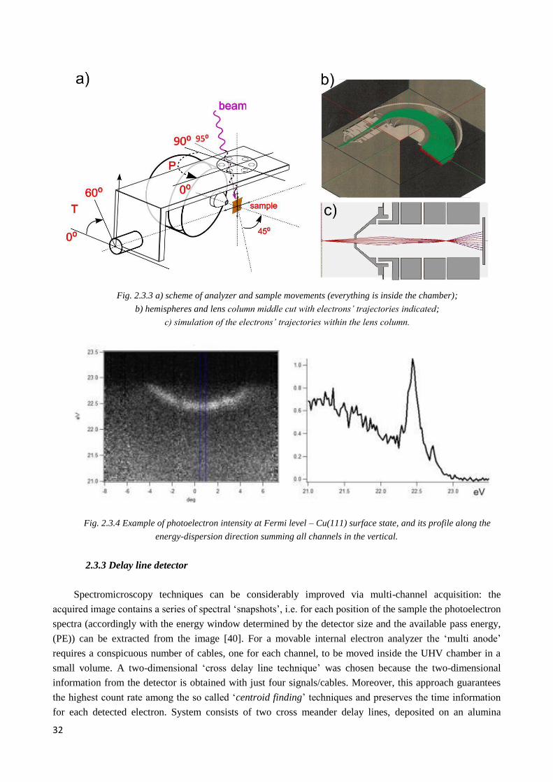
32
Fig. 2.3.3 a) scheme of analyzer and sample movements (everything is inside the chamber);
b) hemispheres and lens column middle cut with electrons’ trajectories indicated;
c) simulation of the electrons’ trajectories within the lens column.
Fig. 2.3.4 Example of photoelectron intensity at Fermi level – Cu(111) surface state, and its profile along the
energy-dispersion direction summing all channels in the vertical.
2.3.3 Delay line detector
Spectromicroscopy techniques can be considerably improved via multi-channel acquisition: the
acquired image contains a series of spectral ‘snapshots’, i.e. for each position of the sample the photoelectron
spectra (accordingly with the energy window determined by the detector size and the available pass energy,
(PE)) can be extracted from the image [40]. For a movable internal electron analyzer the ‘multi anode’
requires a conspicuous number of cables, one for each channel, to be moved inside the UHV chamber in a
small volume. A two-dimensional ‘cross delay line technique’ was chosen because the two-dimensional
information from the detector is obtained with just four signals/cables. Moreover, this approach guarantees
the highest count rate among the so called ‘centroid finding’ techniques and preserves the time information
for each detected electron. System consists of two cross meander delay lines, deposited on an alumina
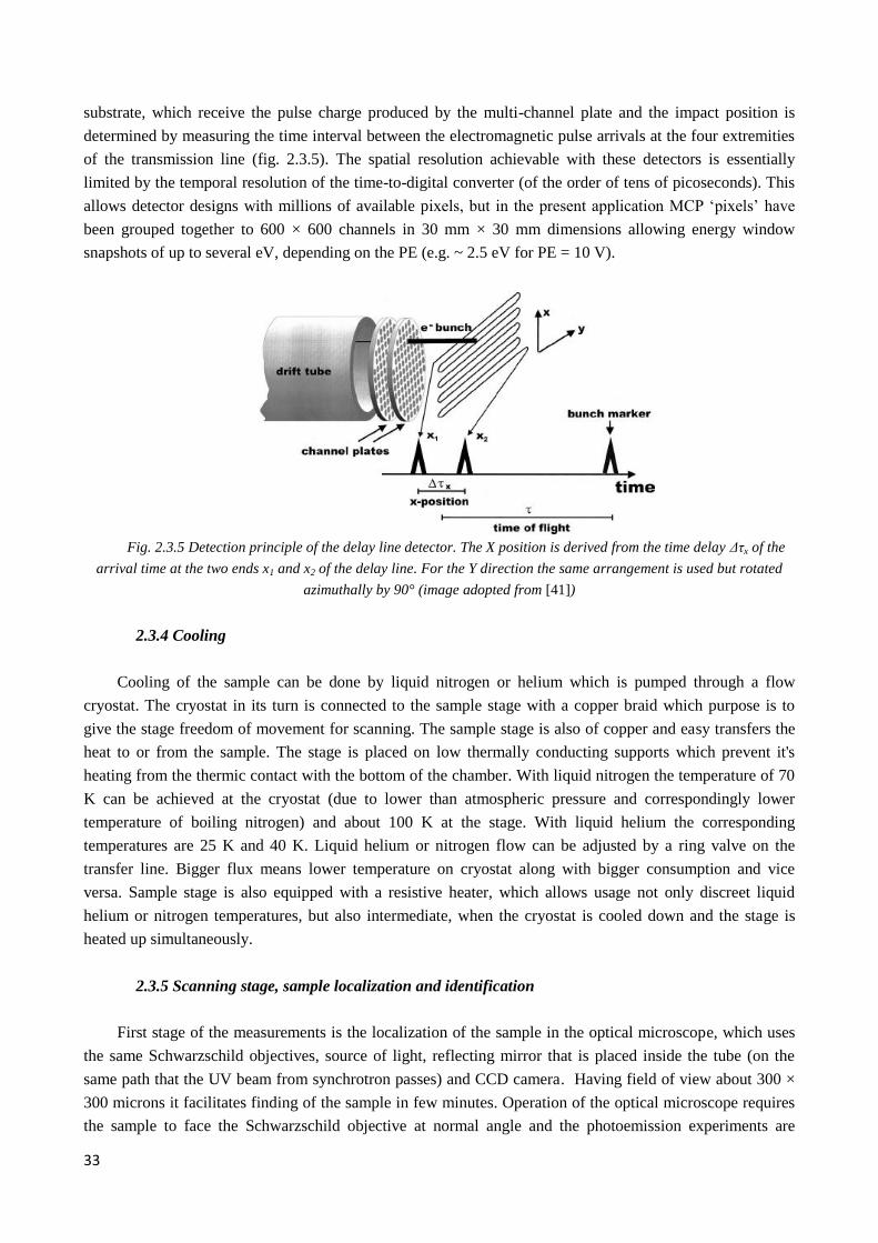
33
substrate, which receive the pulse charge produced by the multi-channel plate and the impact position is
determined by measuring the time interval between the electromagnetic pulse arrivals at the four extremities
of the transmission line (fig. 2.3.5). The spatial resolution achievable with these detectors is essentially
limited by the temporal resolution of the time-to-digital converter (of the order of tens of picoseconds). This
allows detector designs with millions of available pixels, but in the present application MCP ‘pixels’ have
been grouped together to 600 × 600 channels in 30 mm × 30 mm dimensions allowing energy window
snapshots of up to several eV, depending on the PE (e.g. ~ 2.5 eV for PE = 10 V).
Fig. 2.3.5 Detection principle of the delay line detector. The X position is derived from the time delay Δτx of the
arrival time at the two ends x1 and x2 of the delay line. For the Y direction the same arrangement is used but rotated
azimuthally by 90° (image adopted from [41])
2.3.4 Cooling
Cooling of the sample can be done by liquid nitrogen or helium which is pumped through a flow
cryostat. The cryostat in its turn is connected to the sample stage with a copper braid which purpose is to
give the stage freedom of movement for scanning. The sample stage is also of copper and easy transfers the
heat to or from the sample. The stage is placed on low thermally conducting supports which prevent it's
heating from the thermic contact with the bottom of the chamber. With liquid nitrogen the temperature of 70
K can be achieved at the cryostat (due to lower than atmospheric pressure and correspondingly lower
temperature of boiling nitrogen) and about 100 K at the stage. With liquid helium the corresponding
temperatures are 25 K and 40 K. Liquid helium or nitrogen flow can be adjusted by a ring valve on the
transfer line. Bigger flux means lower temperature on cryostat along with bigger consumption and vice
versa. Sample stage is also equipped with a resistive heater, which allows usage not only discreet liquid
helium or nitrogen temperatures, but also intermediate, when the cryostat is cooled down and the stage is
heated up simultaneously.
2.3.5 Scanning stage, sample localization and identification
First stage of the measurements is the localization of the sample in the optical microscope, which uses
the same Schwarzschild objectives, source of light, reflecting mirror that is placed inside the tube (on the
same path that the UV beam from synchrotron passes) and CCD camera. Having field of view about 300 ×
300 microns it facilitates finding of the sample in few minutes. Operation of the optical microscope requires
the sample to face the Schwarzschild objective at normal angle and the photoemission experiments are
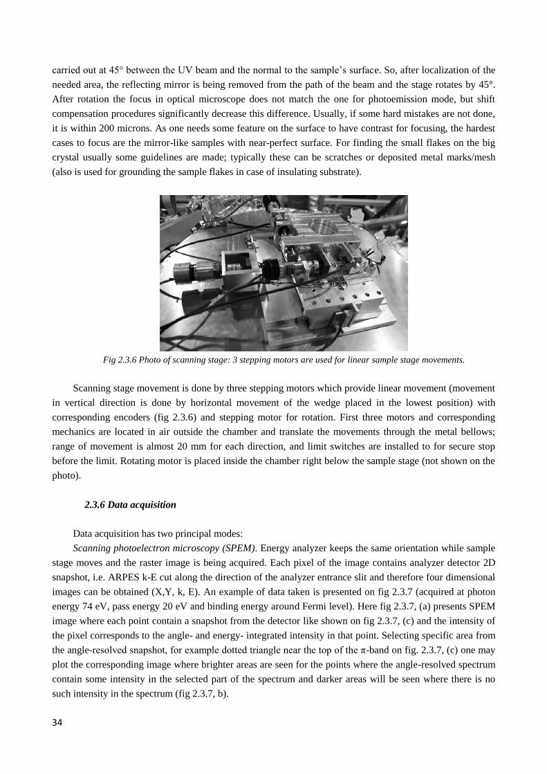
34
carried out at 45° between the UV beam and the normal to the sample’s surface. So, after localization of the
needed area, the reflecting mirror is being removed from the path of the beam and the stage rotates by 45°.
After rotation the focus in optical microscope does not match the one for photoemission mode, but shift
compensation procedures significantly decrease this difference. Usually, if some hard mistakes are not done,
it is within 200 microns. As one needs some feature on the surface to have contrast for focusing, the hardest
cases to focus are the mirror-like samples with near-perfect surface. For finding the small flakes on the big
crystal usually some guidelines are made; typically these can be scratches or deposited metal marks/mesh
(also is used for grounding the sample flakes in case of insulating substrate).
Fig 2.3.6 Photo of scanning stage: 3 stepping motors are used for linear sample stage movements.
Scanning stage movement is done by three stepping motors which provide linear movement (movement
in vertical direction is done by horizontal movement of the wedge placed in the lowest position) with
corresponding encoders (fig 2.3.6) and stepping motor for rotation. First three motors and corresponding
mechanics are located in air outside the chamber and translate the movements through the metal bellows;
range of movement is almost 20 mm for each direction, and limit switches are installed to for secure stop
before the limit. Rotating motor is placed inside the chamber right below the sample stage (not shown on the
photo).
2.3.6 Data acquisition
Data acquisition has two principal modes:
Scanning photoelectron microscopy (SPEM). Energy analyzer keeps the same orientation while sample
stage moves and the raster image is being acquired. Each pixel of the image contains analyzer detector 2D
snapshot, i.e. ARPES k-E cut along the direction of the analyzer entrance slit and therefore four dimensional
images can be obtained (X,Y, k, E). An example of data taken is presented on fig 2.3.7 (acquired at photon
energy 74 eV, pass energy 20 eV and binding energy around Fermi level). Here fig 2.3.7, (a) presents SPEM
image where each point contain a snapshot from the detector like shown on fig 2.3.7, (c) and the intensity of
the pixel corresponds to the angle- and energy- integrated intensity in that point. Selecting specific area from
the angle-resolved snapshot, for example dotted triangle near the top of the π-band on fig. 2.3.7, (c) one may
plot the corresponding image where brighter areas are seen for the points where the angle-resolved spectrum
contain some intensity in the selected part of the spectrum and darker areas will be seen where there is no
such intensity in the spectrum (fig 2.3.7, b).
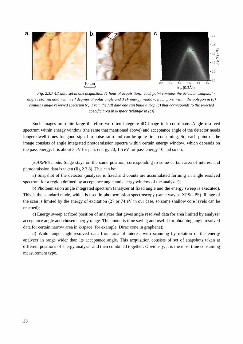
35
Fig. 2.3.7 4D data set in one acquisition (1 hour of acquisition): each point contains the detector ‘snaphot’ -
angle resolved data within 14 degrees of polar angle and 3 eV energy window. Each pixel within the polygon in (a)
contains angle resolved spectrum (c). From the full date one can build a map (c) that corresponds to the selected
specific area in k-space (triangle in (c))
Such images are quite large therefore we often integrate 4D image in k-coordinate. Angle resolved
spectrum within energy window (the same that mentioned above) and acceptance angle of the detector needs
longer dwell times for good signal-to-noise ratio and can be quite time-consuming. So, each point of the
image consists of angle integrated photoemission spectra within certain energy window, which depends on
the pass energy. It is about 3 eV for pass energy 20, 1.5 eV for pass energy 10 and so on.
µ-ARPES mode. Stage stays on the same position, corresponding to some certain area of interest and
photoemission data is taken (fig 2.3.8). This can be:
a) Snapshot of the detector (analyzer is fixed and counts are accumulated forming an angle resolved
spectrum for a region defined by acceptance angle and energy window of the analyzer);
b) Photoemission angle integrated spectrum (analyzer at fixed angle and the energy sweep is executed).
This is the standard mode, which is used in photoemission spectroscopy (same way as XPS/UPS). Range of
the scan is limited by the energy of excitation (27 or 74 eV in our case, so some shallow core levels can be
reached);
c) Energy sweep at fixed position of analyzer that gives angle resolved data for area limited by analyzer
acceptance angle and chosen energy range. This mode is time saving and useful for obtaining angle resolved
data for certain narrow area in k-space (for example, Dirac cone in graphene);
d) Wide range angle-resolved data from area of interest with scanning by rotation of the energy
analyzer in range wider than its acceptance angle. This acquisition consists of set of snapshots taken at
different positions of energy analyzer and then combined together. Obviously, it is the most time consuming
measurement type.
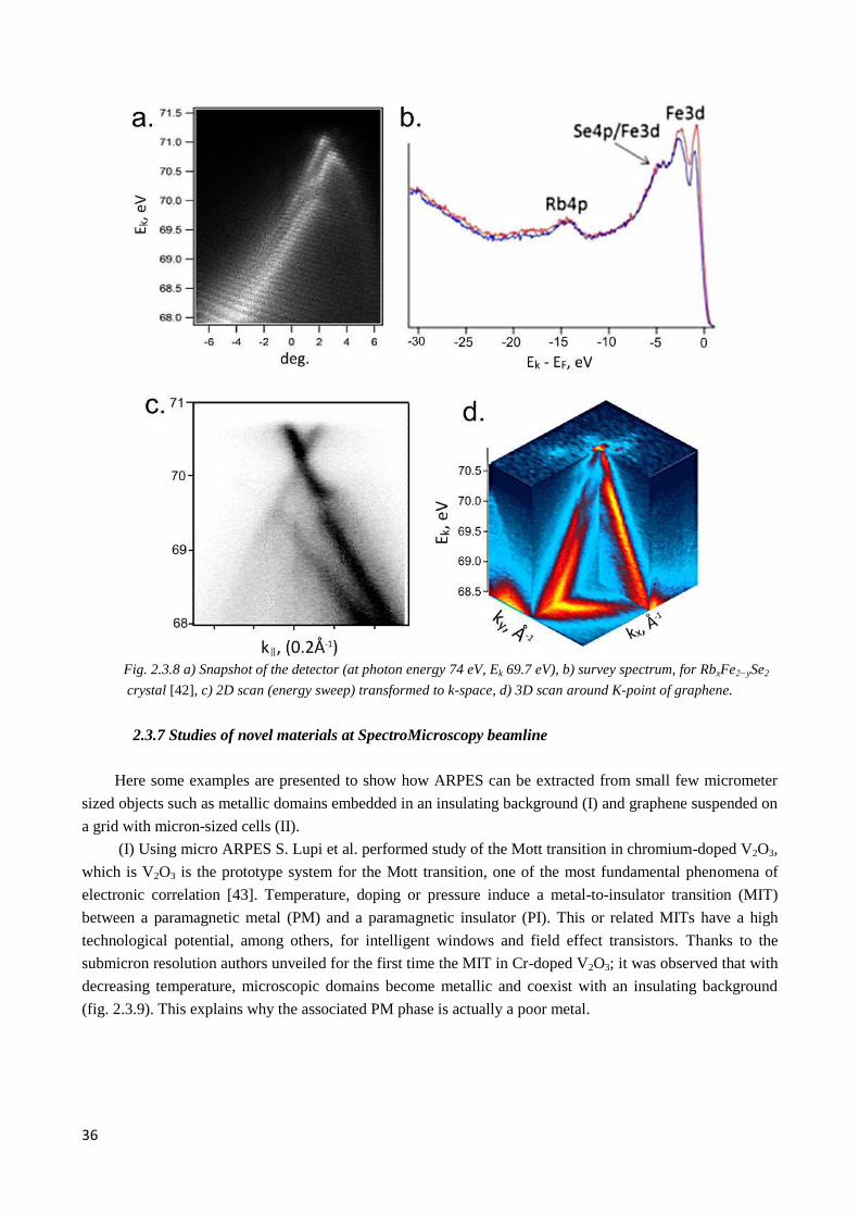
36
Fig. 2.3.8 a) Snapshot of the detector (at photon energy 74 eV, Ek 69.7 eV), b) survey spectrum, for RbxFe2−ySe2
crystal [42], c) 2D scan (energy sweep) transformed to k-space, d) 3D scan around K-point of graphene.
2.3.7 Studies of novel materials at SpectroMicroscopy beamline
Here some examples are presented to show how ARPES can be extracted from small few micrometer
sized objects such as metallic domains embedded in an insulating background (I) and graphene suspended on
a grid with micron-sized cells (II).
(I) Using micro ARPES S. Lupi et al. performed study of the Mott transition in chromium-doped V2O3,
which is V2O3 is the prototype system for the Mott transition, one of the most fundamental phenomena of
electronic correlation [43]. Temperature, doping or pressure induce a metal-to-insulator transition (MIT)
between a paramagnetic metal (PM) and a paramagnetic insulator (PI). This or related MITs have a high
technological potential, among others, for intelligent windows and field effect transistors. Thanks to the
submicron resolution authors unveiled for the first time the MIT in Cr-doped V2O3; it was observed that with
decreasing temperature, microscopic domains become metallic and coexist with an insulating background
(fig. 2.3.9). This explains why the associated PM phase is actually a poor metal.
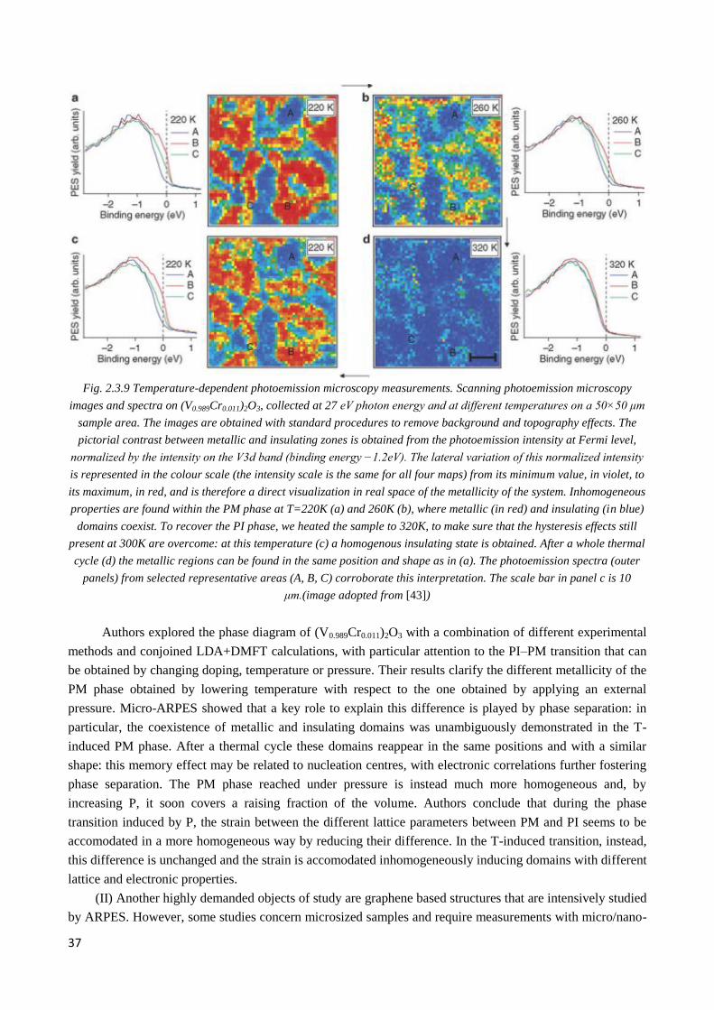
37
Fig. 2.3.9 Temperature-dependent photoemission microscopy measurements. Scanning photoemission microscopy
images and spectra on (V0.989Cr0.011)2O3, collected at 27 eV photon energy and at different temperatures on a 50×50 μm
sample area. The images are obtained with standard procedures to remove background and topography effects. The
pictorial contrast between metallic and insulating zones is obtained from the photoemission intensity at Fermi level,
normalized by the intensity on the V3d band (binding energy −1.2eV). The lateral variation of this normalized intensity
is represented in the colour scale (the intensity scale is the same for all four maps) from its minimum value, in violet, to
its maximum, in red, and is therefore a direct visualization in real space of the metallicity of the system. Inhomogeneous
properties are found within the PM phase at T=220K (a) and 260K (b), where metallic (in red) and insulating (in blue)
domains coexist. To recover the PI phase, we heated the sample to 320K, to make sure that the hysteresis effects still
present at 300K are overcome: at this temperature (c) a homogenous insulating state is obtained. After a whole thermal
cycle (d) the metallic regions can be found in the same position and shape as in (a). The photoemission spectra (outer
panels) from selected representative areas (A, B, C) corroborate this interpretation. The scale bar in panel c is 10
μm.(image adopted from [43])
Authors explored the phase diagram of (V0.989Cr0.011)2O3 with a combination of different experimental
methods and conjoined LDA+DMFT calculations, with particular attention to the PI–PM transition that can
be obtained by changing doping, temperature or pressure. Their results clarify the different metallicity of the
PM phase obtained by lowering temperature with respect to the one obtained by applying an external
pressure. Micro-ARPES showed that a key role to explain this difference is played by phase separation: in
particular, the coexistence of metallic and insulating domains was unambiguously demonstrated in the T-
induced PM phase. After a thermal cycle these domains reappear in the same positions and with a similar
shape: this memory effect may be related to nucleation centres, with electronic correlations further fostering
phase separation. The PM phase reached under pressure is instead much more homogeneous and, by
increasing P, it soon covers a raising fraction of the volume. Authors conclude that during the phase
transition induced by P, the strain between the different lattice parameters between PM and PI seems to be
accomodated in a more homogeneous way by reducing their difference. In the T-induced transition, instead,
this difference is unchanged and the strain is accomodated inhomogeneously inducing domains with different
lattice and electronic properties.
(II) Another highly demanded objects of study are graphene based structures that are intensively studied
by ARPES. However, some studies concern microsized samples and require measurements with micro/nano-
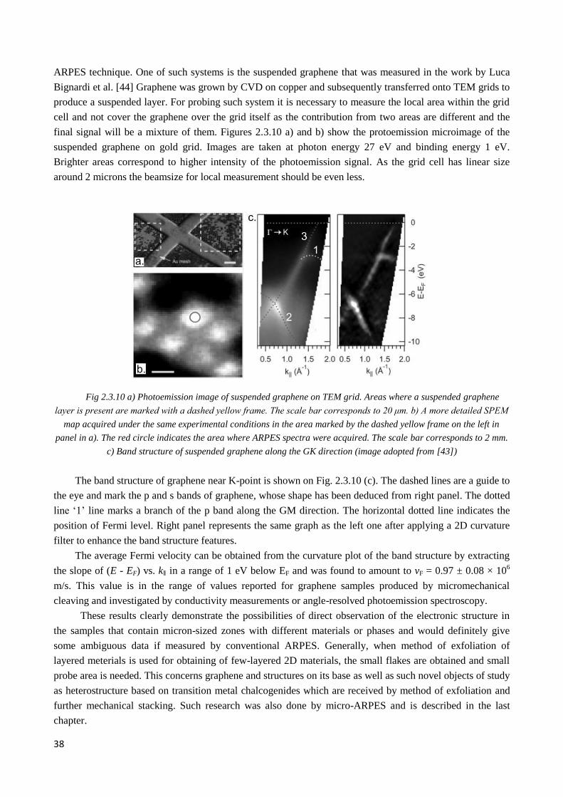
38
ARPES technique. One of such systems is the suspended graphene that was measured in the work by Luca
Bignardi et al. [44] Graphene was grown by CVD on copper and subsequently transferred onto TEM grids to
produce a suspended layer. For probing such system it is necessary to measure the local area within the grid
cell and not cover the graphene over the grid itself as the contribution from two areas are different and the
final signal will be a mixture of them. Figures 2.3.10 a) and b) show the protoemission microimage of the
suspended graphene on gold grid. Images are taken at photon energy 27 eV and binding energy 1 eV.
Brighter areas correspond to higher intensity of the photoemission signal. As the grid cell has linear size
around 2 microns the beamsize for local measurement should be even less.
Fig 2.3.10 a) Photoemission image of suspended graphene on TEM grid. Areas where a suspended graphene
layer is present are marked with a dashed yellow frame. The scale bar corresponds to 20 μm. b) A more detailed SPEM
map acquired under the same experimental conditions in the area marked by the dashed yellow frame on the left in
panel in a). The red circle indicates the area where ARPES spectra were acquired. The scale bar corresponds to 2 mm.
c) Band structure of suspended graphene along the GK direction (image adopted from [43])
The band structure of graphene near K-point is shown on Fig. 2.3.10 (c). The dashed lines are a guide to
the eye and mark the p and s bands of graphene, whose shape has been deduced from right panel. The dotted
line ‘1’ line marks a branch of the p band along the GM direction. The horizontal dotted line indicates the
position of Fermi level. Right panel represents the same graph as the left one after applying a 2D curvature
filter to enhance the band structure features.
The average Fermi velocity can be obtained from the curvature plot of the band structure by extracting
the slope of (E - EF) vs. k∥ in a range of 1 eV below EF and was found to amount to vF = 0.97 ± 0.08 × 10⁶
m/s. This value is in the range of values reported for graphene samples produced by micromechanical
cleaving and investigated by conductivity measurements or angle-resolved photoemission spectroscopy.
These results clearly demonstrate the possibilities of direct observation of the electronic structure in
the samples that contain micron-sized zones with different materials or phases and would definitely give
some ambiguous data if measured by conventional ARPES. Generally, when method of exfoliation of
layered meterials is used for obtaining of few-layered 2D materials, the small flakes are obtained and small
probe area is needed. This concerns graphene and structures on its base as well as such novel objects of study
as heterostructure based on transition metal chalcogenides which are received by method of exfoliation and
further mechanical stacking. Such research was also done by micro-ARPES and is described in the last
chapter.
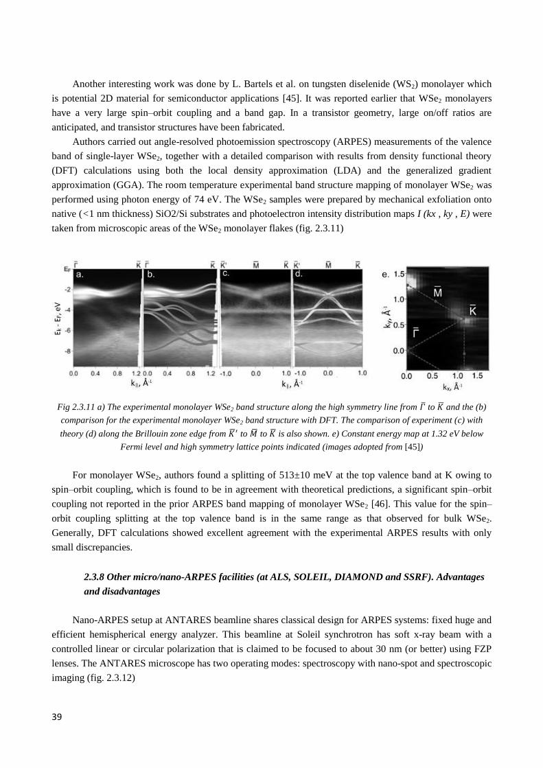
39
Another interesting work was done by L. Bartels et al. on tungsten diselenide (WS2) monolayer which
is potential 2D material for semiconductor applications [45]. It was reported earlier that WSe2 monolayers
have a very large spin–orbit coupling and a band gap. In a transistor geometry, large on/off ratios are
anticipated, and transistor structures have been fabricated.
Authors carried out angle-resolved photoemission spectroscopy (ARPES) measurements of the valence
band of single-layer WSe2, together with a detailed comparison with results from density functional theory
(DFT) calculations using both the local density approximation (LDA) and the generalized gradient
approximation (GGA). The room temperature experimental band structure mapping of monolayer WSe2 was
performed using photon energy of 74 eV. The WSe2 samples were prepared by mechanical exfoliation onto
native (<1 nm thickness) SiO2/Si substrates and photoelectron intensity distribution maps I (kx , ky , E) were
taken from microscopic areas of the WSe2 monolayer flakes (fig. 2.3.11)
Fig 2.3.11 a) The experimental monolayer WSe2 band structure along the high symmetry line from 𝛤 to 𝐾 and the (b)
comparison for the experimental monolayer WSe2 band structure with DFT. The comparison of experiment (c) with
theory (d) along the Brillouin zone edge from 𝐾′ to �� to 𝐾 is also shown. e) Constant energy map at 1.32 eV below
Fermi level and high symmetry lattice points indicated (images adopted from [45])
For monolayer WSe2, authors found a splitting of 513±10 meV at the top valence band at K owing to
spin–orbit coupling, which is found to be in agreement with theoretical predictions, a significant spin–orbit
coupling not reported in the prior ARPES band mapping of monolayer WSe2 [46]. This value for the spin–
orbit coupling splitting at the top valence band is in the same range as that observed for bulk WSe2.
Generally, DFT calculations showed excellent agreement with the experimental ARPES results with only
small discrepancies.
2.3.8 Other micro/nano-ARPES facilities (at ALS, SOLEIL, DIAMOND and SSRF). Advantages
and disadvantages
Nano-ARPES setup at ANTARES beamline shares classical design for ARPES systems: fixed huge and
efficient hemispherical energy analyzer. This beamline at Soleil synchrotron has soft x-ray beam with a
controlled linear or circular polarization that is claimed to be focused to about 30 nm (or better) using FZP
lenses. The ANTARES microscope has two operating modes: spectroscopy with nano-spot and spectroscopic
imaging (fig. 2.3.12)
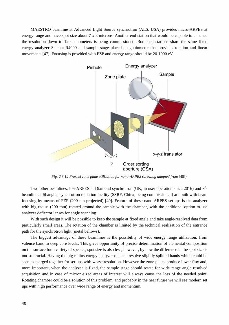
40
MAESTRO beamline at Advanced Light Source synchrotron (ALS, USA) provides micro-ARPES at
energy range and have spot size about 7 x 8 microns. Another end-station that would be capable to enhance
the resolution down to 120 nanometers is being commissioned. Both end stations share the same fixed
energy analyzer Scienta R4000 and sample stage placed on goniometer that provides rotation and linear
movements [47]. Focusing is provided with FZP and energy range should be 20-1000 eV
Fig. 2.3.12 Fresnel zone plate utilization for nano-ARPES (drawing adopted from [48])
Two other beamlines, I05-ARPES at Diamond synchrotron (UK, in user operation since 2016) and S2-
beamline at Shanghai synchrotron radiation facility (SSRF, China, being commissioned) are built with beam
focusing by means of FZP (200 nm projected) [49]. Feature of these nano-ARPES set-ups is the analyzer
with big radius (200 mm) rotated around the sample with the chamber, with the additional option to use
analyzer deflector lenses for angle scanning.
With such design it will be possible to keep the sample at fixed angle and take angle-resolved data from
particularly small areas. The rotation of the chamber is limited by the technical realization of the entrance
path for the synchrotron light (metal bellows).
The biggest advantage of these beamlines is the possibility of wide energy range utilization: from
valence band to deep core levels. This gives opportunity of precise determination of elemental composition
on the surface for a variety of species, spot size is also less, however, by now the difference in the spot size is
not so crucial. Having the big radius energy analyzer one can resolve slightly splitted bands which could be
seen as merged together for set-ups with worse resolution. However the zone plates produce lower flux and,
more important, when the analyzer is fixed, the sample stage should rotate for wide range angle resolved
acquisition and in case of micron-sized areas of interest will always cause the loss of the needed point.
Rotating chamber could be a solution of this problem, and probably in the near future we will see modern set
ups with high performance over wide range of energy and momentum.

41
2.3.9 Summary and further development
Thus, SpectroMicroscopy beamline is a powerful and unique instrument which allows photoemission
imaging of the samples with submicron resolution and acquiring of angle resolved photoemission data from
of micron sized samples or specific sample’s area. Effective way of finding the right area of interest and
putting the sample into beam focus saves much time that is crucial for avoiding sample degradation,
contamination and simply leaving more time for useful measurements. Measurements can be done at wide
range of temperatures that gives opportunity to observe the electronic structure change for phase transitions.
Beamline is being continuously improved in both software and hardware aspects. New features to the
program packages are added to increase safety and convenience of work, μ-metal shield was inserted inside
the main chamber to improve work al low electron energies. Vacuum, scanning and cooling systems also
undergo improvements.
42
3. Graphene electronic structure and synthesis
Graphene, a two-dimensional hexagonal carbon lattice, is one of the most studied materials today
because of its unique electronic properties which allow it to be used in future high-performant
nanoelectronics. 2D carbon lattice was theoretically described as a building block of graphite 3D structure
long time before the first obtaining. Starting from 1970’s single layers of graphite were grown on top of
other materials. This "epitaxial graphene" consisted of a single-atom-thick hexagonal lattice of sp2-bonded
carbon atoms, as in free-standing graphene. However, charge transfer from the substrate to the epitaxial
graphene and in some cases d-orbitals of the substrate atoms hybridize with the π-orbitals of graphene and
significantly alter its electronic structure. This layer, next to the substrate, is so-called “buffer layer” and has
much less carrier mobility with respect to free-standing graphene.
Efforts to make thin films of graphite by mechanical exfoliation started in 1990, but nothing thinner than 50
to 100 layers was produced before 2000. In 2004 monolayer graphene was obtained by mechanical
exfoliation and then transferred onto SiO2 substrate by A. Geim and K. Novoselov at the University of
Manchester [50]. Their substrate, SiO2 layer, weakly interacted with graphene, providing nearly charge-
neutral graphene layers.
Graphene is a zero-gap semiconductor, its conduction and valence bands meet at Dirac points. Each
atom has four bonds, one σ bond with each of its three neighbors and one π-bond that is oriented out of
plane. The atoms are about 1.42 Å apart, and electronic structure of graphene is represented by Dirac points,
six locations in momentum space, on the edge of the Brillouin zone.
Graphene's stability is due to its tightly packed carbon atoms and sp2 orbital hybridization – a
combination of orbitals s, px and py that constitute σ-bond. The final pz electron makes up π-bond. π-bonds
hybridize together to form π-band and π∗-bands. These bands are responsible for most of graphene's notable
electronic properties, via the half-filled band that permits free-moving electrons. [51]
Electrons propagating through graphene's honeycomb lattice effectively lose their mass, producing
quasiparticles that are described by a 2D analogue of Dirac equation. Due to discovered unique graphene
properties as enormous electrical and thermal conductivity a huge research activity began and today many
potential fields of graphene’s application appeared:
1. Membranes (water filtration, gas separation, water desalination, food and pharmaceutical
packaging).
2. Composites and coatings (composite materials including graphene).
3. Energy (graphene in batteries, supercapacitors).
4. Biomedical (graphene can serve as a platform for drug delivery and ultrasensitive biosensors).
5. Sensors (each atom of the graphene is exposed to its environment allowing it to sense changes in its
surroundings; opens possibilities of supersensitive sensors including military application for sensing
chemical warfare agents and explosives).
6. Electronics (graphene semiconductors, high mobility field effect transistors, wearable technology,
improving touch screens).
In general, isolated 2D crystals cannot be grown via chemical synthesis beyond small sizes even in
principle, because the rapid growth of phonon density with increasing lateral size forces 2D crystallites to
bend into the third dimension, so for growth of 2D material some kind of support is needed.
Today a variety of graphene production techniques are reported: exfoliation with subsequent transfer on
specific substrate, chemical vapor deposition (CVD), shearing, sonification, SiC thermal decomposition,
43
molecular beam deposition, carbon segregation from the bulk of the metal substrate and many others.
Graphene nanoribbons can be created by cutting open carbon nanotubes. In one such method multi-walled
carbon nanotubes are cut open in solution by action of potassium permanganate and sulfuric acid. In another
method graphene nanoribbons were produced by plasma etching of nanotubes partly embedded in a polymer
film. [52, 53]
Not all this methods are prospective for commercial applications. For example, monolayer exfoliation
can produce only small flakes of quasi-random geometry and is considered to be a research technique
suitable for making not more than proof-of-concept devices. For large scale production CVD method is more
promising.
A major deterrent to graphene’s application in digital electronic devices is the lack of an intrinsic band
gap, which is needed large enough to provide clear contrast between a transistor’s ‘on’ and ‘off’ states, so
that it could process information without generating errors. Along with the creation of the bandgap another
requirement would be to preserve the linear dispersion in order benefit the high mobility of the charge
carriers. The creation of a local band gap in graphene may be achieved by coupling the π-bands of
graphene’s two sublattices, which in the past has been accomplished in a number of different ways, like
hydrogenation, fluorination, removal of carbon atoms, interactions with various substrates, etc. In graphene
bilayer systems it can further be achieved by creation of an interlayer asymmetry either by surface doping or
a perpendicular electric field. [54, 55, 56, 57] One possible solution to this problem is graphene nanoribbons,
which have a band gap inversely proportional to their width due to quantum confinement [58]. Initial
methods for their manufacture involved cutting ribbons from larger sheets, resulting in disordered edges
detrimental to transport. Recently, though, graphene nanoribbons as narrow as 40 nm have been grown
directly on nanofacets in SiC surfaces, preserving their structural integrity, this discovery has motivated the
interest in studying other surface orientations of SiC. [59]
Removing the substrate is the possible way to improve the carrier mobility. Such structure, so called
‘suspended graphene’, is thought to be suitable for electronic components as well as for chemical sensors or
nano-membranes. Suspended graphene can be prepared by exfoliation of the one or few carbon layers layers
with further transfer onto metallic grid or by CVD synthesis with further chemical etching the underlying
SiO2. It was reported that suspended graphene demonstrates transport properties which are close to the
theoretical predictions for isolated graphene [60]. Studies by transmission electron microscopy reveal that
suspended graphene sheets are not perfectly flat: they exhibit intrinsic microscopic roughening ("rippling"),
such that the surface normal varies by several degrees and out-of-plane deformations reach 1 nm [61]. These
ripples may be intrinsic to the material as a result of the instability of two-dimensional crystals, [62] or may
originate from the ubiquitous dirt seen in all TEM images of graphene.
Summarizing, direct view on band structure by ARPES still remains challenging for many graphene
based systems, because often the requirements of the sample’s purity are hard to fulfill (due to use of
solvents) and, most importantly, usually small areas have to be measured.
3.1 Electronic properties of graphene
The origin of Dirac spectrum of low-energy excitations can be understood using a nearest-neighbor
tight-binding model on a hexagonal lattice, which provides an adequate description of the graphene band
structure. The honeycomb graphene lattice, illustrated in fig. 3.1.1, has two non-equivalent sublattices, A and
B. Within the tight-binding model, which includes only nearest-neighbor hopping, the energy gap vanishes at
the two non-equivalent Brillouin zone corners, K and K'.
In the case of two atoms per unit cell one may write the wavefunction as
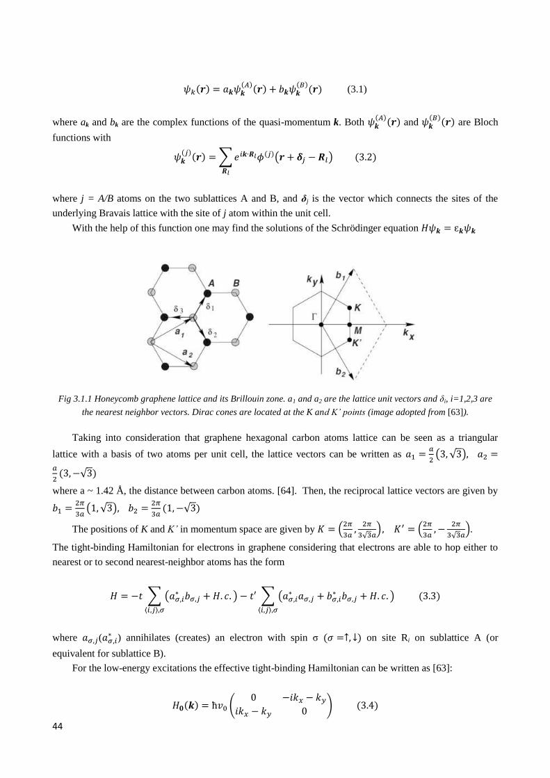
44
𝜓𝑘(𝒓) = 𝑎𝒌𝜓𝒌(𝐴)
(𝒓) + 𝑏𝒌𝜓𝒌(𝐵)
(𝒓) (3.1)
where ak and bk are the complex functions of the quasi-momentum k. Both 𝜓𝒌(𝐴)(𝒓) and 𝜓𝒌
(𝐵)(𝒓) are Bloch
functions with
𝜓𝒌(𝑗)
(𝒓) = ∑ 𝑒𝑖𝒌∙𝑹𝑙𝜙(𝑗)(𝒓 + 𝜹𝑗 − 𝑹𝑙)
𝑹𝑙
(3.2)
where j = A/B atoms on the two sublattices A and B, and δj is the vector which connects the sites of the
underlying Bravais lattice with the site of j atom within the unit cell.
With the help of this function one may find the solutions of the Schrödinger equation 𝐻𝜓𝒌 = ɛ𝒌𝜓𝒌
Fig 3.1.1 Honeycomb graphene lattice and its Brillouin zone. a1 and a2 are the lattice unit vectors and δi, i=1,2,3 are
the nearest neighbor vectors. Dirac cones are located at the K and K’ points (image adopted from [63]).
Taking into consideration that graphene hexagonal carbon atoms lattice can be seen as a triangular
lattice with a basis of two atoms per unit cell, the lattice vectors can be written as 𝑎1 =𝑎
2(3, √3), 𝑎2 =
𝑎
2(3, −√3)
where a ~ 1.42 Å, the distance between carbon atoms. [64]. Then, the reciprocal lattice vectors are given by
𝑏1 =2𝜋
3𝑎(1, √3), 𝑏2 =
2𝜋
3𝑎(1, −√3)
The positions of K and K’ in momentum space are given by 𝐾 = (2𝜋
3𝑎,
2𝜋
3√3𝑎), 𝐾′ = (
2𝜋
3𝑎, −
2𝜋
3√3𝑎).
The tight-binding Hamiltonian for electrons in graphene considering that electrons are able to hop either to
nearest or to second nearest-neighbor atoms has the form
𝐻 = −𝑡 ∑ (𝑎𝜎,𝑖∗ 𝑏𝜎,𝑗 + 𝐻. 𝑐. )
⟨𝑖,𝑗⟩,𝜎
− 𝑡′ ∑ (𝑎𝜎,𝑖∗ 𝑎𝜎,𝑗 + 𝑏𝜎,𝑖
∗ 𝑏𝜎,𝑗 + 𝐻. 𝑐. )⟨𝑖,𝑗⟩,𝜎
(3.3)
where 𝑎𝜎,𝑗(𝑎𝜎,𝑖∗ ) annihilates (creates) an electron with spin σ (𝜎 =↑, ↓) on site Ri on sublattice A (or
equivalent for sublattice B).
For the low-energy excitations the effective tight-binding Hamiltonian can be written as [63]:
𝐻𝟎(𝒌) = ħ𝑣0 (0 −𝑖𝑘𝑥 − 𝑘𝑦
𝑖𝑘𝑥 − 𝑘𝑦 0) (3.4)
45
where 𝑣0 is Fermi velocity and k is the small wavevector of the quasiparticle near K-point. The energy
spectrum of this Hamiltonian is ɛ(𝒌) = 𝑠ħ𝑣0𝒌, where s is +1 or -1 for an eigenstate above or below Dirac-
point energy, which is defined to be the energy zero, respectively.
Eigenstates of this Hamiltonian are given by
⟨𝒓|𝑠, 𝒌⟩ =1
√2𝑒𝑖𝒌∙𝒓 (
1𝑖𝑠𝑒𝑖𝜃𝒌) (3.5)
Two values (for s +1 and -1) derive from the existence of two sublattices, that are like two degrees of
freedom, and the electron can have an amplitude of the Bloch funchtion on sublattice A, and an amplitude on
the sublattice B. The presence of the sublattice basis {|𝐴⟩, |𝐵⟩} resembles the case with spin one-half particle,
where an electron can be in spin-up state |↑⟩, spin-down state |↓⟩, or any superposition of these. The
sublattice basis is therefore called pseudospin or isospin.
Thus, the dispersion relation around K-point is linear and the biggest difference between this result and
usual case, ɛ(q)=q2/2m, where m is the effective electron mass, is that Fermi velocity does not depend on the
energy or momentum. In usual case it is 𝑣 = 𝑘/𝑚 = √2𝐸/𝑚.
As the resulting differential equation for movement of graphene’s quasiparticles is equivalent to Dirac
equation, hence charge carriers in the vicinity of EF may be termed “Dirac fermions” (with the crossing point
at K being named Dirac point). Moreover, the particular band structure at the BZ boundary (that is, a linear
dispersion) leads to an effective mass m* = 0 at the point where the VB and CB meet.
This peculiar band structure in ultrathin graphite layers results in a number of unusual electronic
transport properties, such as unusual half-integer quantum Hall effect and Klein tunneling effect.
Moreover, the particles described by Dirac Hamiltonian of monolayer graphene have yet another
property: they are chiral; this means that the orientation of pseudospin depends on the direction of the
momentum. Owing to their chiral nature, the propagation of charge carriers in external periodic potential is
highly anisotropic, and in extreme cases results in group velocities that are reduced to zero in one direction
but are unchanged in another. C.-H. Peer and others showed that the density and type of carrier species
(electron, hole or open orbit) in a graphene superlattice are extremely sensitive to the potential applied, and
they may further be tuned by varying Fermi level [65]. Calculation carried out by authors clearly showed that
in presence of periodic potential applied to the graphene monolayer Fermi velocity is anisotropically
renormalized. Calculations showed that the anisotropy disappears if the chiral nature of the states in
graphene is intentionally removed. Thus, anisotropic gap opening at the minizone boundary (MB) also was
demonstrated to result from pseudospin nature of charge carriers in graphene. Here the chosen period of the
applied potential is bigger than graphene’s unit cell and the superlattice formed as a result of superposition of
the latter ones has unit cell bigger, than in graphene. Thus the resulting reciprocal lattice has smaller base
vector and the new Brillouin zone is also smaller, so it is often named minizone (mBZ). Its boundary
similarly to the Brillouin zone is built up by the perpendicular planes in the middle between the points of the
reciprocal lattice. The question of superlattices and minizones will be described more for case of rotated
graphene bilayers and moiré patterns in chapter 3.4.1.
The name pseudospin is given because the physics of Dirac fermions in graphene is similar to Fermion
particles and one can think of pseudo-spintronic devices in the same way as in the field of spintronics [66]. It
should be clear, however, that as soon as the electron is transferred away from graphene the notion of
pseudo-spin has no sense anymore. Besides the band gap the overlapping π-bands create non-smooth points
in the density of states, namely Van Hove singularities, which are described below.
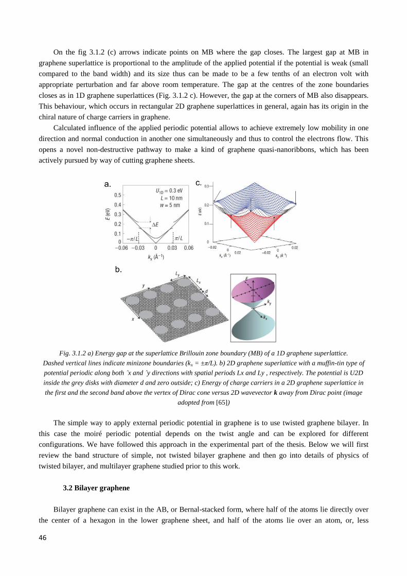
46
On the fig 3.1.2 (c) arrows indicate points on MB where the gap closes. The largest gap at MB in
graphene superlattice is proportional to the amplitude of the applied potential if the potential is weak (small
compared to the band width) and its size thus can be made to be a few tenths of an electron volt with
appropriate perturbation and far above room temperature. The gap at the centres of the zone boundaries
closes as in 1D graphene superlattices (Fig. 3.1.2 c). However, the gap at the corners of MB also disappears.
This behaviour, which occurs in rectangular 2D graphene superlattices in general, again has its origin in the
chiral nature of charge carriers in graphene.
Calculated influence of the applied periodic potential allows to achieve extremely low mobility in one
direction and normal conduction in another one simultaneously and thus to control the electrons flow. This
opens a novel non-destructive pathway to make a kind of graphene quasi-nanoribbons, which has been
actively pursued by way of cutting graphene sheets.
Fig. 3.1.2 a) Energy gap at the superlattice Brillouin zone boundary (MB) of a 1D graphene superlattice.
Dashed vertical lines indicate minizone boundaries (kx = ±π/L). b) 2D graphene superlattice with a muffin-tin type of
potential periodic along both ˆx and ˆy directions with spatial periods Lx and Ly , respectively. The potential is U2D
inside the grey disks with diameter d and zero outside; c) Energy of charge carriers in a 2D graphene superlattice in
the first and the second band above the vertex of Dirac cone versus 2D wavevector k away from Dirac point (image
adopted from [65])
The simple way to apply external periodic potential in graphene is to use twisted graphene bilayer. In
this case the moiré periodic potential depends on the twist angle and can be explored for different
configurations. We have followed this approach in the experimental part of the thesis. Below we will first
review the band structure of simple, not twisted bilayer graphene and then go into details of physics of
twisted bilayer, and multilayer graphene studied prior to this work.
3.2 Bilayer graphene
Bilayer graphene can exist in the AB, or Bernal-stacked form, where half of the atoms lie directly over
the center of a hexagon in the lower graphene sheet, and half of the atoms lie over an atom, or, less
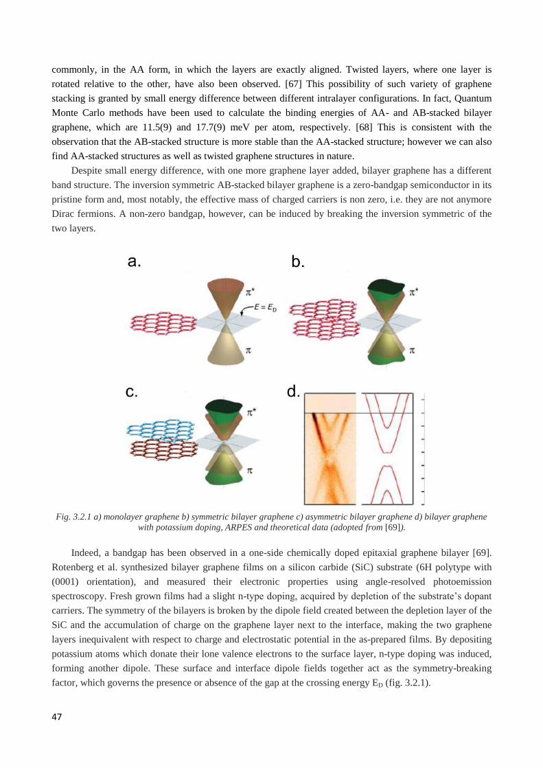
47
commonly, in the AA form, in which the layers are exactly aligned. Twisted layers, where one layer is
rotated relative to the other, have also been observed. [67] This possibility of such variety of graphene
stacking is granted by small energy difference between different intralayer configurations. In fact, Quantum
Monte Carlo methods have been used to calculate the binding energies of AA- and AB-stacked bilayer
graphene, which are 11.5(9) and 17.7(9) meV per atom, respectively. [68] This is consistent with the
observation that the AB-stacked structure is more stable than the AA-stacked structure; however we can also
find AA-stacked structures as well as twisted graphene structures in nature.
Despite small energy difference, with one more graphene layer added, bilayer graphene has a different
band structure. The inversion symmetric AB-stacked bilayer graphene is a zero-bandgap semiconductor in its
pristine form and, most notably, the effective mass of charged carriers is non zero, i.e. they are not anymore
Dirac fermions. A non-zero bandgap, however, can be induced by breaking the inversion symmetric of the
two layers.
Fig. 3.2.1 a) monolayer graphene b) symmetric bilayer graphene c) asymmetric bilayer graphene d) bilayer graphene
with potassium doping, ARPES and theoretical data (adopted from [69]).
Indeed, a bandgap has been observed in a one-side chemically doped epitaxial graphene bilayer [69].
Rotenberg et al. synthesized bilayer graphene films on a silicon carbide (SiC) substrate (6H polytype with
(0001) orientation), and measured their electronic properties using angle-resolved photoemission
spectroscopy. Fresh grown films had a slight n-type doping, acquired by depletion of the substrate’s dopant
carriers. The symmetry of the bilayers is broken by the dipole field created between the depletion layer of the
SiC and the accumulation of charge on the graphene layer next to the interface, making the two graphene
layers inequivalent with respect to charge and electrostatic potential in the as-prepared films. By depositing
potassium atoms which donate their lone valence electrons to the surface layer, n-type doping was induced,
forming another dipole. These surface and interface dipole fields together act as the symmetry-breaking
factor, which governs the presence or absence of the gap at the crossing energy ED (fig. 3.2.1).
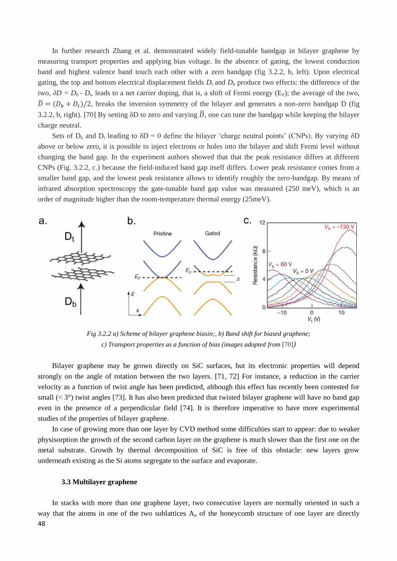
48
In further research Zhang et al. demonstrated widely field-tunable bandgap in bilayer graphene by
measuring transport properties and applying bias voltage. In the absence of gating, the lowest conduction
band and highest valence band touch each other with a zero bandgap (fig 3.2.2, b, left). Upon electrical
gating, the top and bottom electrical displacement fields Dt and Db produce two effects: the difference of the
two, δD = Db - Dt, leads to a net carrier doping, that is, a shift of Fermi energy (EF); the average of the two,
�� = (𝐷𝑏 + 𝐷𝑡)/2, breaks the inversion symmetry of the bilayer and generates a non-zero bandgap D (fig
3.2.2, b, right). [70] By setting δD to zero and varying ��, one can tune the bandgap while keeping the bilayer
charge neutral.
Sets of Db and Dt leading to δD = 0 define the bilayer ‘charge neutral points’ (CNPs). By varying δD
above or below zero, it is possible to inject electrons or holes into the bilayer and shift Fermi level without
changing the band gap. In the experiment authors showed that that the peak resistance differs at different
CNPs (Fig. 3.2.2, c.) because the field-induced band gap itself differs. Lower peak resistance comes from a
smaller band gap, and the lowest peak resistance allows to identify roughly the zero-bandgap. By means of
infrared absorption spectroscopy the gate-tunable band gap value was measured (250 meV), which is an
order of magnitude higher than the room-temperature thermal energy (25meV).
Fig 3.2.2 a) Scheme of bilayer graphene biasin;, b) Band shift for biased graphene;
c) Transport properties as a function of bias (images adopted from [70])
Bilayer graphene may be grown directly on SiC surfaces, but its electronic properties will depend
strongly on the angle of rotation between the two layers. [71, 72] For instance, a reduction in the carrier
velocity as a function of twist angle has been predicted, although this effect has recently been contested for
small (< 3°) twist angles [73]. It has also been predicted that twisted bilayer graphene will have no band gap
even in the presence of a perpendicular field [74]. It is therefore imperative to have more experimental
studies of the properties of bilayer graphene.
In case of growing more than one layer by CVD method some difficulties start to appear: due to weaker
physisorption the growth of the second carbon layer on the graphene is much slower than the first one on the
metal substrate. Growth by thermal decomposition of SiC is free of this obstacle: new layers grow
underneath existing as the Si atoms segregate to the surface and evaporate.
3.3 Multilayer graphene
In stacks with more than one graphene layer, two consecutive layers are normally oriented in such a
way that the atoms in one of the two sublattices An of the honeycomb structure of one layer are directly
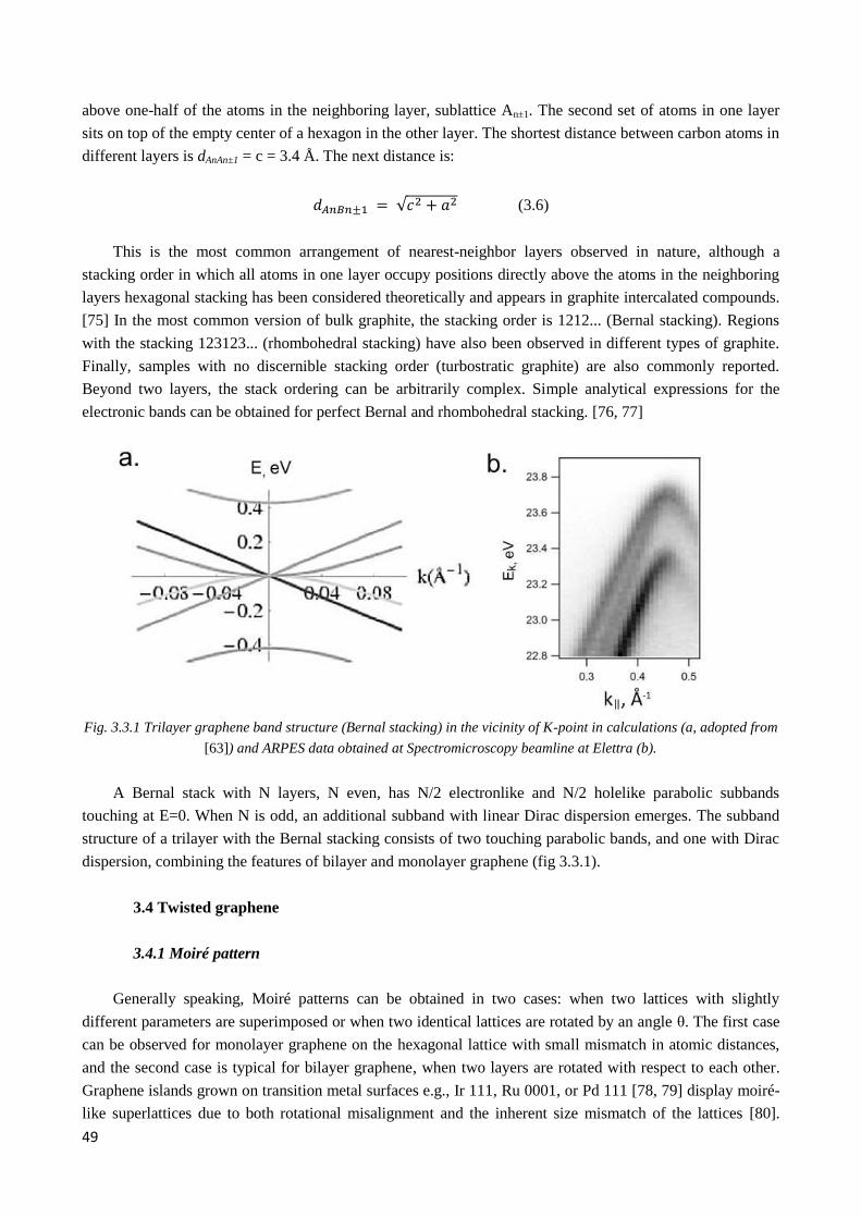
49
above one-half of the atoms in the neighboring layer, sublattice An±1. The second set of atoms in one layer
sits on top of the empty center of a hexagon in the other layer. The shortest distance between carbon atoms in
different layers is dAnAn±1 = c = 3.4 Å. The next distance is:
𝑑𝐴𝑛𝐵𝑛±1 = √𝑐2 + 𝑎2 (3.6)
This is the most common arrangement of nearest-neighbor layers observed in nature, although a
stacking order in which all atoms in one layer occupy positions directly above the atoms in the neighboring
layers hexagonal stacking has been considered theoretically and appears in graphite intercalated compounds.
[75] In the most common version of bulk graphite, the stacking order is 1212... (Bernal stacking). Regions
with the stacking 123123... (rhombohedral stacking) have also been observed in different types of graphite.
Finally, samples with no discernible stacking order (turbostratic graphite) are also commonly reported.
Beyond two layers, the stack ordering can be arbitrarily complex. Simple analytical expressions for the
electronic bands can be obtained for perfect Bernal and rhombohedral stacking. [76, 77]
Fig. 3.3.1 Trilayer graphene band structure (Bernal stacking) in the vicinity of K-point in calculations (a, adopted from
[63]) and ARPES data obtained at Spectromicroscopy beamline at Elettra (b).
A Bernal stack with N layers, N even, has N/2 electronlike and N/2 holelike parabolic subbands
touching at E=0. When N is odd, an additional subband with linear Dirac dispersion emerges. The subband
structure of a trilayer with the Bernal stacking consists of two touching parabolic bands, and one with Dirac
dispersion, combining the features of bilayer and monolayer graphene (fig 3.3.1).
3.4 Twisted graphene
3.4.1 Moiré pattern
Generally speaking, Moiré patterns can be obtained in two cases: when two lattices with slightly
different parameters are superimposed or when two identical lattices are rotated by an angle θ. The first case
can be observed for monolayer graphene on the hexagonal lattice with small mismatch in atomic distances,
and the second case is typical for bilayer graphene, when two layers are rotated with respect to each other.
Graphene islands grown on transition metal surfaces e.g., Ir 111, Ru 0001, or Pd 111 [78, 79] display moiré-
like superlattices due to both rotational misalignment and the inherent size mismatch of the lattices [80].
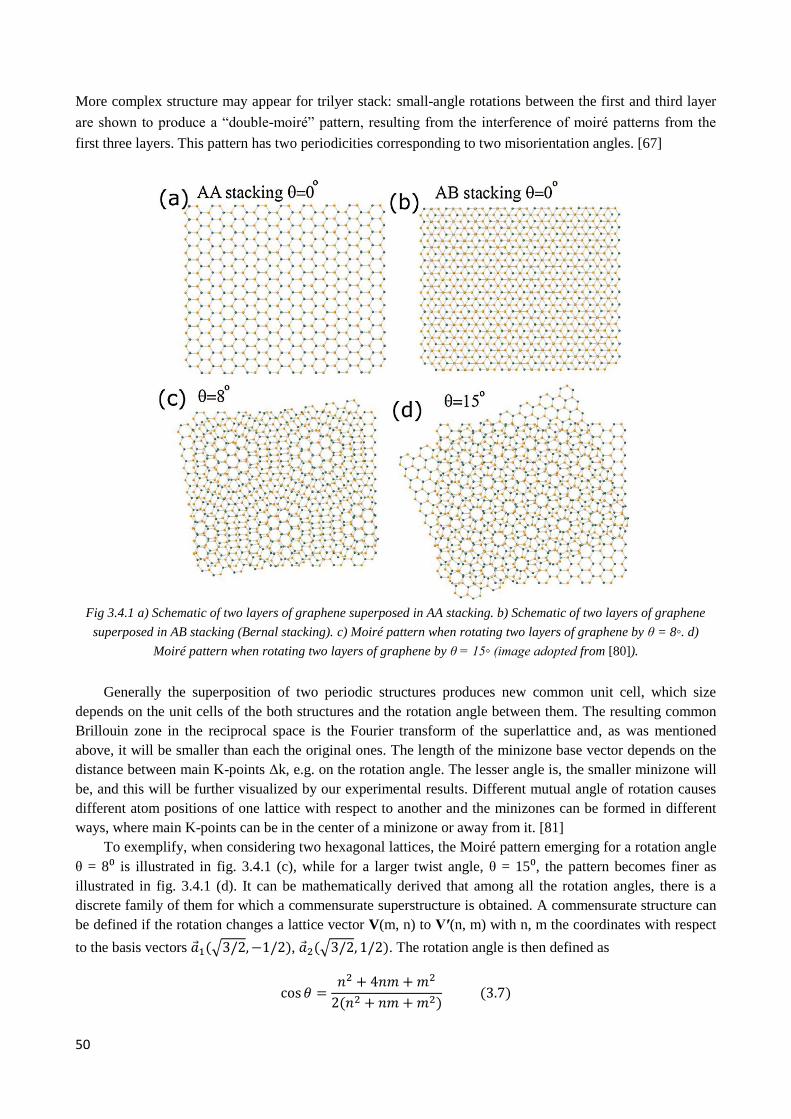
50
More complex structure may appear for trilyer stack: small-angle rotations between the first and third layer
are shown to produce a “double-moiré” pattern, resulting from the interference of moiré patterns from the
first three layers. This pattern has two periodicities corresponding to two misorientation angles. [67]
Fig 3.4.1 a) Schematic of two layers of graphene superposed in AA stacking. b) Schematic of two layers of graphene
superposed in AB stacking (Bernal stacking). c) Moiré pattern when rotating two layers of graphene by θ = 8◦. d)
Moiré pattern when rotating two layers of graphene by θ = 15◦ (image adopted from [80]).
Generally the superposition of two periodic structures produces new common unit cell, which size
depends on the unit cells of the both structures and the rotation angle between them. The resulting common
Brillouin zone in the reciprocal space is the Fourier transform of the superlattice and, as was mentioned
above, it will be smaller than each the original ones. The length of the minizone base vector depends on the
distance between main K-points Δk, e.g. on the rotation angle. The lesser angle is, the smaller minizone will
be, and this will be further visualized by our experimental results. Different mutual angle of rotation causes
different atom positions of one lattice with respect to another and the minizones can be formed in different
ways, where main K-points can be in the center of a minizone or away from it. [81]
To exemplify, when considering two hexagonal lattices, the Moiré pattern emerging for a rotation angle
θ = 8⁰ is illustrated in fig. 3.4.1 (c), while for a larger twist angle, θ = 15⁰, the pattern becomes finer as
illustrated in fig. 3.4.1 (d). It can be mathematically derived that among all the rotation angles, there is a
discrete family of them for which a commensurate superstructure is obtained. A commensurate structure can
be defined if the rotation changes a lattice vector V(m, n) to V′(n, m) with n, m the coordinates with respect
to the basis vectors ��1(√3/2, −1/2), ��2(√3/2, 1/2). The rotation angle is then defined as
cos 𝜃 =𝑛2 + 4𝑛𝑚 + 𝑚2
2(𝑛2 + 𝑛𝑚 + 𝑚2) (3.7)
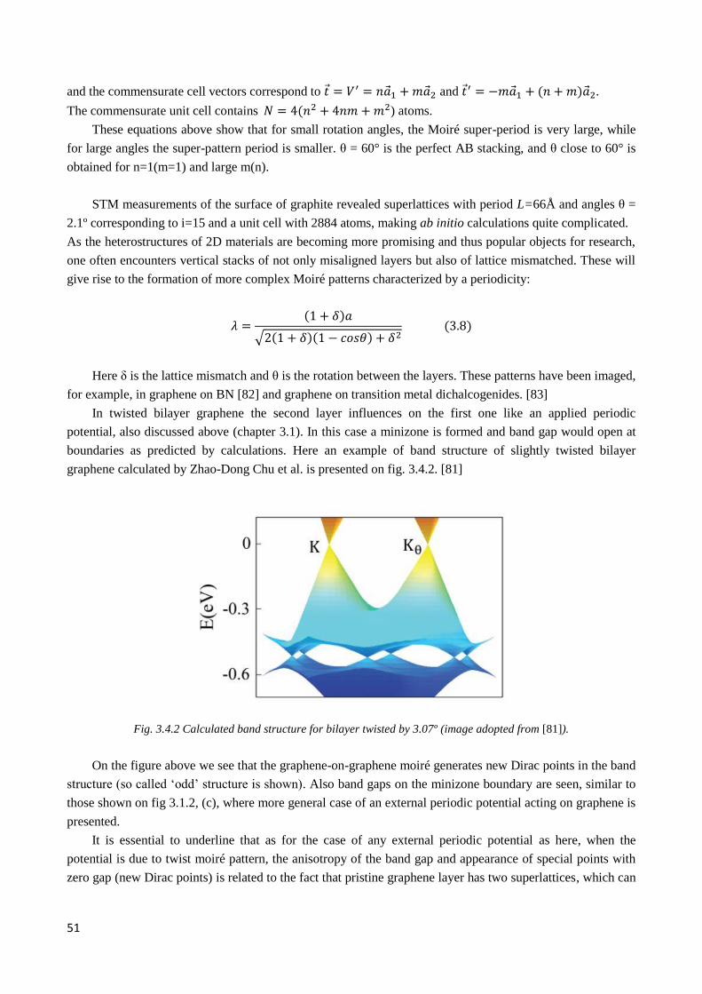
51
and the commensurate cell vectors correspond to 𝑡 = 𝑉′ = 𝑛��1 + 𝑚��2 and 𝑡′ = −𝑚��1 + (𝑛 + 𝑚)��2.
The commensurate unit cell contains 𝑁 = 4(𝑛2 + 4𝑛𝑚 + 𝑚2) atoms.
These equations above show that for small rotation angles, the Moiré super-period is very large, while
for large angles the super-pattern period is smaller. θ = 60° is the perfect AB stacking, and θ close to 60° is
obtained for n=1(m=1) and large m(n).
STM measurements of the surface of graphite revealed superlattices with period L=66Å and angles θ =
2.1º corresponding to i=15 and a unit cell with 2884 atoms, making ab initio calculations quite complicated.
As the heterostructures of 2D materials are becoming more promising and thus popular objects for research,
one often encounters vertical stacks of not only misaligned layers but also of lattice mismatched. These will
give rise to the formation of more complex Moiré patterns characterized by a periodicity:
𝜆 =(1 + 𝛿)𝑎
√2(1 + 𝛿)(1 − 𝑐𝑜𝑠𝜃) + 𝛿2 (3.8)
Here δ is the lattice mismatch and θ is the rotation between the layers. These patterns have been imaged,
for example, in graphene on BN [82] and graphene on transition metal dichalcogenides. [83]
In twisted bilayer graphene the second layer influences on the first one like an applied periodic
potential, also discussed above (chapter 3.1). In this case a minizone is formed and band gap would open at
boundaries as predicted by calculations. Here an example of band structure of slightly twisted bilayer
graphene calculated by Zhao-Dong Chu et al. is presented on fig. 3.4.2. [81]
Fig. 3.4.2 Calculated band structure for bilayer twisted by 3.07º (image adopted from [81]).
On the figure above we see that the graphene-on-graphene moiré generates new Dirac points in the band
structure (so called ‘odd’ structure is shown). Also band gaps on the minizone boundary are seen, similar to
those shown on fig 3.1.2, (c), where more general case of an external periodic potential acting on graphene is
presented.
It is essential to underline that as for the case of any external periodic potential as here, when the
potential is due to twist moiré pattern, the anisotropy of the band gap and appearance of special points with
zero gap (new Dirac points) is related to the fact that pristine graphene layer has two superlattices, which can
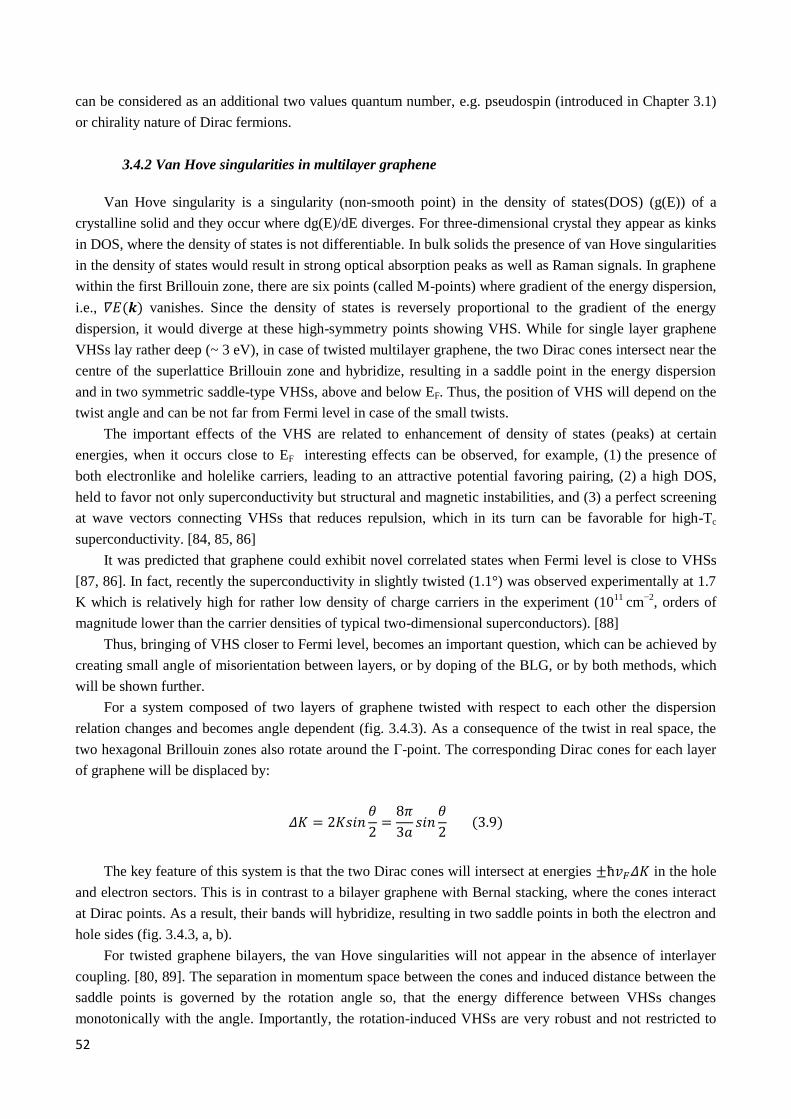
52
can be considered as an additional two values quantum number, e.g. pseudospin (introduced in Chapter 3.1)
or chirality nature of Dirac fermions.
3.4.2 Van Hove singularities in multilayer graphene
Van Hove singularity is a singularity (non-smooth point) in the density of states(DOS) (g(E)) of a
crystalline solid and they occur where dg(E)/dE diverges. For three-dimensional crystal they appear as kinks
in DOS, where the density of states is not differentiable. In bulk solids the presence of van Hove singularities
in the density of states would result in strong optical absorption peaks as well as Raman signals. In graphene
within the first Brillouin zone, there are six points (called M-points) where gradient of the energy dispersion,
i.e., 𝛻𝐸(𝒌) vanishes. Since the density of states is reversely proportional to the gradient of the energy
dispersion, it would diverge at these high-symmetry points showing VHS. While for single layer graphene
VHSs lay rather deep (~ 3 eV), in case of twisted multilayer graphene, the two Dirac cones intersect near the
centre of the superlattice Brillouin zone and hybridize, resulting in a saddle point in the energy dispersion
and in two symmetric saddle-type VHSs, above and below EF. Thus, the position of VHS will depend on the
twist angle and can be not far from Fermi level in case of the small twists.
The important effects of the VHS are related to enhancement of density of states (peaks) at certain
energies, when it occurs close to EF interesting effects can be observed, for example, (1) the presence of
both electronlike and holelike carriers, leading to an attractive potential favoring pairing, (2) a high DOS,
held to favor not only superconductivity but structural and magnetic instabilities, and (3) a perfect screening
at wave vectors connecting VHSs that reduces repulsion, which in its turn can be favorable for high-Tc
superconductivity. [84, 85, 86]
It was predicted that graphene could exhibit novel correlated states when Fermi level is close to VHSs
[87, 86]. In fact, recently the superconductivity in slightly twisted (1.1°) was observed experimentally at 1.7
K which is relatively high for rather low density of charge carriers in the experiment (1011
cm−2
, orders of
magnitude lower than the carrier densities of typical two-dimensional superconductors). [88]
Thus, bringing of VHS closer to Fermi level, becomes an important question, which can be achieved by
creating small angle of misorientation between layers, or by doping of the BLG, or by both methods, which
will be shown further.
For a system composed of two layers of graphene twisted with respect to each other the dispersion
relation changes and becomes angle dependent (fig. 3.4.3). As a consequence of the twist in real space, the
two hexagonal Brillouin zones also rotate around the Г-point. The corresponding Dirac cones for each layer
of graphene will be displaced by:
𝛥𝐾 = 2𝐾𝑠𝑖𝑛𝜃
2=
8𝜋
3𝑎𝑠𝑖𝑛
𝜃
2 (3.9)
The key feature of this system is that the two Dirac cones will intersect at energies ±ħ𝑣𝐹𝛥𝐾 in the hole
and electron sectors. This is in contrast to a bilayer graphene with Bernal stacking, where the cones interact
at Dirac points. As a result, their bands will hybridize, resulting in two saddle points in both the electron and
hole sides (fig. 3.4.3, a, b).
For twisted graphene bilayers, the van Hove singularities will not appear in the absence of interlayer
coupling. [80, 89]. The separation in momentum space between the cones and induced distance between the
saddle points is governed by the rotation angle so, that the energy difference between VHSs changes
monotonically with the angle. Importantly, the rotation-induced VHSs are very robust and not restricted to

53
the case of two layers. For example, in the case of a trilayer, where the top single layer of graphene is rotated
above a Bernal-stacked bilayer (or even turbo-stacked), VHSs are also preserved. This allows observation of
the multiple VHSs on multilayer graphene samples. Experimentally this can be probed by scanning tunneling
spectroscopy for any specific area where moiré pattern was observed. At very small angles, less than 2º, van
Hove singularities become so dominating that massless Dirac fermions does not describe the electronic states
anymore.
Further research by I. Brihuega et al. confirmed appearance of van Hove singularities for slightly
twisted bilayer graphene using STS together with theoretical calculations. [90] Their measurements show
presence of van Hove singularities due to interlayer coupling that are ubiquitously present in a broad range
(from 1º to 10º) of rotation angles in graphene on 6H-SiC (0001) samples. From the variation of the energy
separation of VHSs with the rotation angle it is possible to recover Fermi velocity of a graphene monolayer
as well as the strength of the interlayer interaction.
Fig 3.4.3 a) Fermi velocity renormalization. Solid line is a theoretical prediction according to Eq. (3.12). Triangles are
from experimental data (image adopted from [89]); b) Scanning tunneling spectroscopy data acquired on Moiré
patterns with rotation angle 1.8º; c) Velocity ratio VBL /VML for a commensurate (n, m) bilayer cell versus rotation angle
θ: circles – ab initio; crosses – TB calculations (image adopted from [91]).
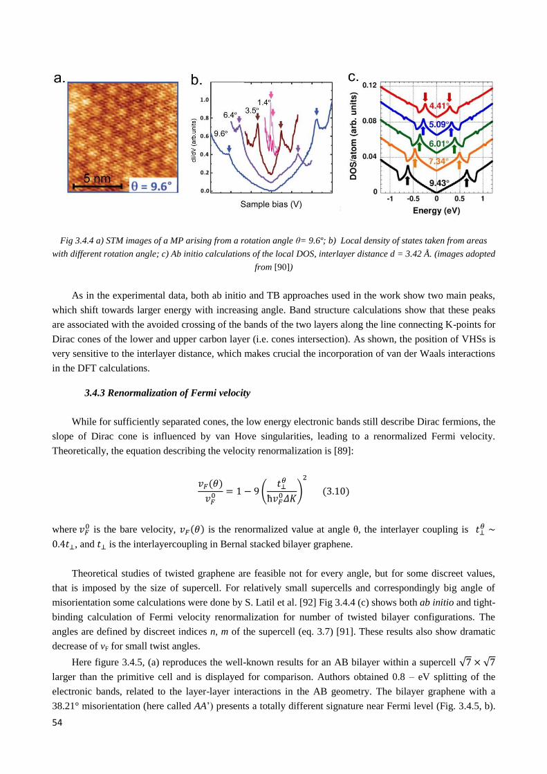
54
Fig 3.4.4 a) STM images of a MP arising from a rotation angle θ= 9.6º; b) Local density of states taken from areas
with different rotation angle; c) Ab initio calculations of the local DOS, interlayer distance d = 3.42 Å. (images adopted
from [90])
As in the experimental data, both ab initio and TB approaches used in the work show two main peaks,
which shift towards larger energy with increasing angle. Band structure calculations show that these peaks
are associated with the avoided crossing of the bands of the two layers along the line connecting K-points for
Dirac cones of the lower and upper carbon layer (i.e. cones intersection). As shown, the position of VHSs is
very sensitive to the interlayer distance, which makes crucial the incorporation of van der Waals interactions
in the DFT calculations.
3.4.3 Renormalization of Fermi velocity
While for sufficiently separated cones, the low energy electronic bands still describe Dirac fermions, the
slope of Dirac cone is influenced by van Hove singularities, leading to a renormalized Fermi velocity.
Theoretically, the equation describing the velocity renormalization is [89]:
𝑣𝐹(𝜃)
𝑣𝐹0 = 1 − 9 (
𝑡⊥𝜃
ħ𝑣𝐹0𝛥𝐾
)
2
(3.10)
where 𝑣𝐹0 is the bare velocity, 𝑣𝐹(𝜃) is the renormalized value at angle θ, the interlayer coupling is 𝑡⊥
𝜃 ∼
0.4𝑡⊥, and 𝑡⊥ is the interlayercoupling in Bernal stacked bilayer graphene.
Theoretical studies of twisted graphene are feasible not for every angle, but for some discreet values,
that is imposed by the size of supercell. For relatively small supercells and correspondingly big angle of
misorientation some calculations were done by S. Latil et al. [92] Fig 3.4.4 (c) shows both ab initio and tight-
binding calculation of Fermi velocity renormalization for number of twisted bilayer configurations. The
angles are defined by discreet indices n, m of the supercell (eq. 3.7) [91]. These results also show dramatic
decrease of vF for small twist angles.
Here figure 3.4.5, (a) reproduces the well-known results for an AB bilayer within a supercell √7 × √7
larger than the primitive cell and is displayed for comparison. Authors obtained 0.8 – eV splitting of the
electronic bands, related to the layer-layer interactions in the AB geometry. The bilayer graphene with a
38.21° misorientation (here called AA’) presents a totally different signature near Fermi level (Fig. 3.4.5, b).
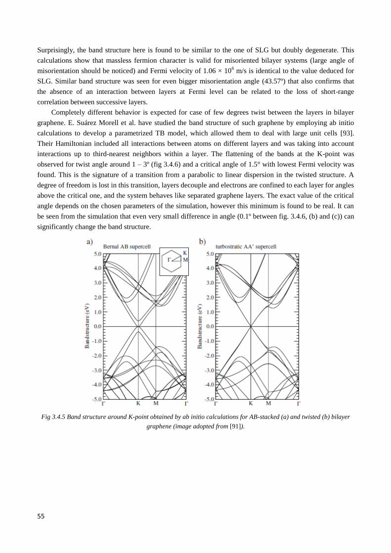
55
Surprisingly, the band structure here is found to be similar to the one of SLG but doubly degenerate. This
calculations show that massless fermion character is valid for misoriented bilayer systems (large angle of
misorientation should be noticed) and Fermi velocity of 1.06 × 10⁶ m/s is identical to the value deduced for
SLG. Similar band structure was seen for even bigger misorientation angle (43.57º) that also confirms that
the absence of an interaction between layers at Fermi level can be related to the loss of short-range
correlation between successive layers.
Completely different behavior is expected for case of few degrees twist between the layers in bilayer
graphene. E. Suárez Morell et al. have studied the band structure of such graphene by employing ab initio
calculations to develop a parametrized TB model, which allowed them to deal with large unit cells [93].
Their Hamiltonian included all interactions between atoms on different layers and was taking into account
interactions up to third-nearest neighbors within a layer. The flattening of the bands at the K-point was
observed for twist angle around 1 – 3º (fig 3.4.6) and a critical angle of 1.5° with lowest Fermi velocity was
found. This is the signature of a transition from a parabolic to linear dispersion in the twisted structure. A
degree of freedom is lost in this transition, layers decouple and electrons are confined to each layer for angles
above the critical one, and the system behaves like separated graphene layers. The exact value of the critical
angle depends on the chosen parameters of the simulation, however this minimum is found to be real. It can
be seen from the simulation that even very small difference in angle (0.1º between fig. 3.4.6, (b) and (c)) can
significantly change the band structure.
Fig 3.4.5 Band structure around K-point obtained by ab initio calculations for AB-stacked (a) and twisted (b) bilayer
graphene (image adopted from [91]).
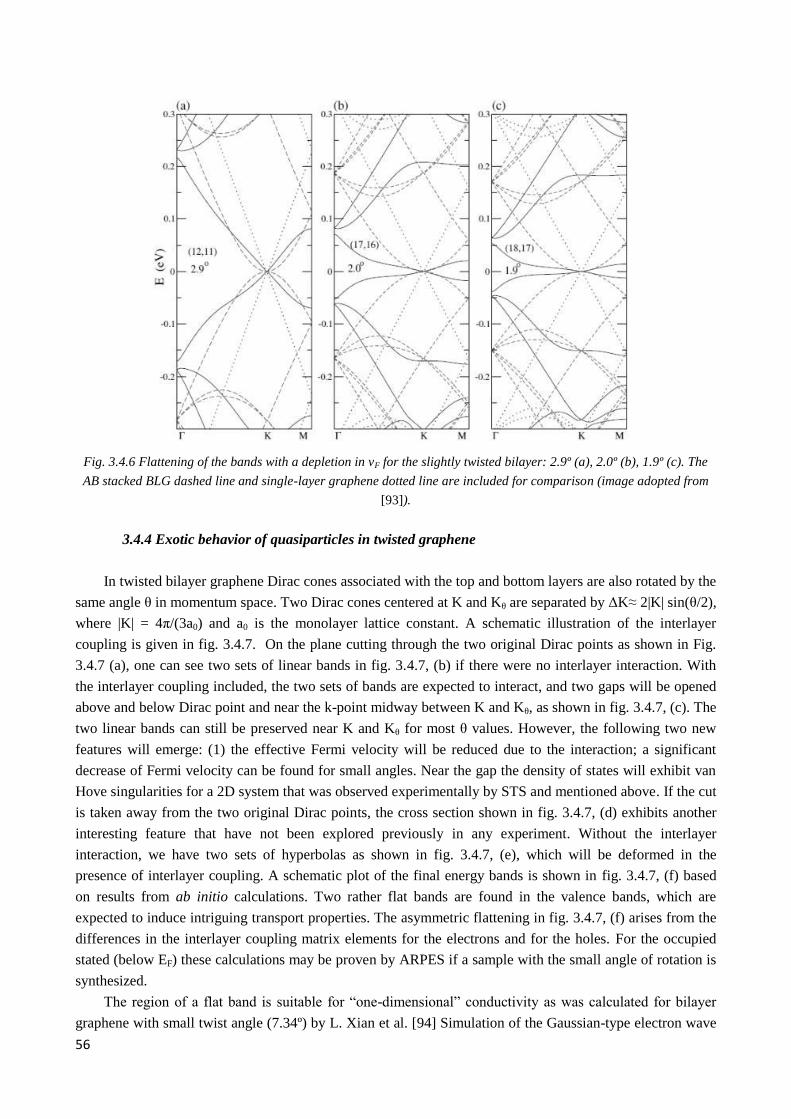
56
Fig. 3.4.6 Flattening of the bands with a depletion in vF for the slightly twisted bilayer: 2.9º (a), 2.0º (b), 1.9º (c). The
AB stacked BLG dashed line and single-layer graphene dotted line are included for comparison (image adopted from
[93]).
3.4.4 Exotic behavior of quasiparticles in twisted graphene
In twisted bilayer graphene Dirac cones associated with the top and bottom layers are also rotated by the
same angle θ in momentum space. Two Dirac cones centered at K and Kθ are separated by ΔK≈ 2|K| sin(θ/2),
where |K| = 4π/(3a0) and a0 is the monolayer lattice constant. A schematic illustration of the interlayer
coupling is given in fig. 3.4.7. On the plane cutting through the two original Dirac points as shown in Fig.
3.4.7 (a), one can see two sets of linear bands in fig. 3.4.7, (b) if there were no interlayer interaction. With
the interlayer coupling included, the two sets of bands are expected to interact, and two gaps will be opened
above and below Dirac point and near the k-point midway between K and Kθ, as shown in fig. 3.4.7, (c). The
two linear bands can still be preserved near K and Kθ for most θ values. However, the following two new
features will emerge: (1) the effective Fermi velocity will be reduced due to the interaction; a significant
decrease of Fermi velocity can be found for small angles. Near the gap the density of states will exhibit van
Hove singularities for a 2D system that was observed experimentally by STS and mentioned above. If the cut
is taken away from the two original Dirac points, the cross section shown in fig. 3.4.7, (d) exhibits another
interesting feature that have not been explored previously in any experiment. Without the interlayer
interaction, we have two sets of hyperbolas as shown in fig. 3.4.7, (e), which will be deformed in the
presence of interlayer coupling. A schematic plot of the final energy bands is shown in fig. 3.4.7, (f) based
on results from ab initio calculations. Two rather flat bands are found in the valence bands, which are
expected to induce intriguing transport properties. The asymmetric flattening in fig. 3.4.7, (f) arises from the
differences in the interlayer coupling matrix elements for the electrons and for the holes. For the occupied
stated (below EF) these calculations may be proven by ARPES if a sample with the small angle of rotation is
synthesized.
The region of a flat band is suitable for “one-dimensional” conductivity as was calculated for bilayer
graphene with small twist angle (7.34º) by L. Xian et al. [94] Simulation of the Gaussian-type electron wave
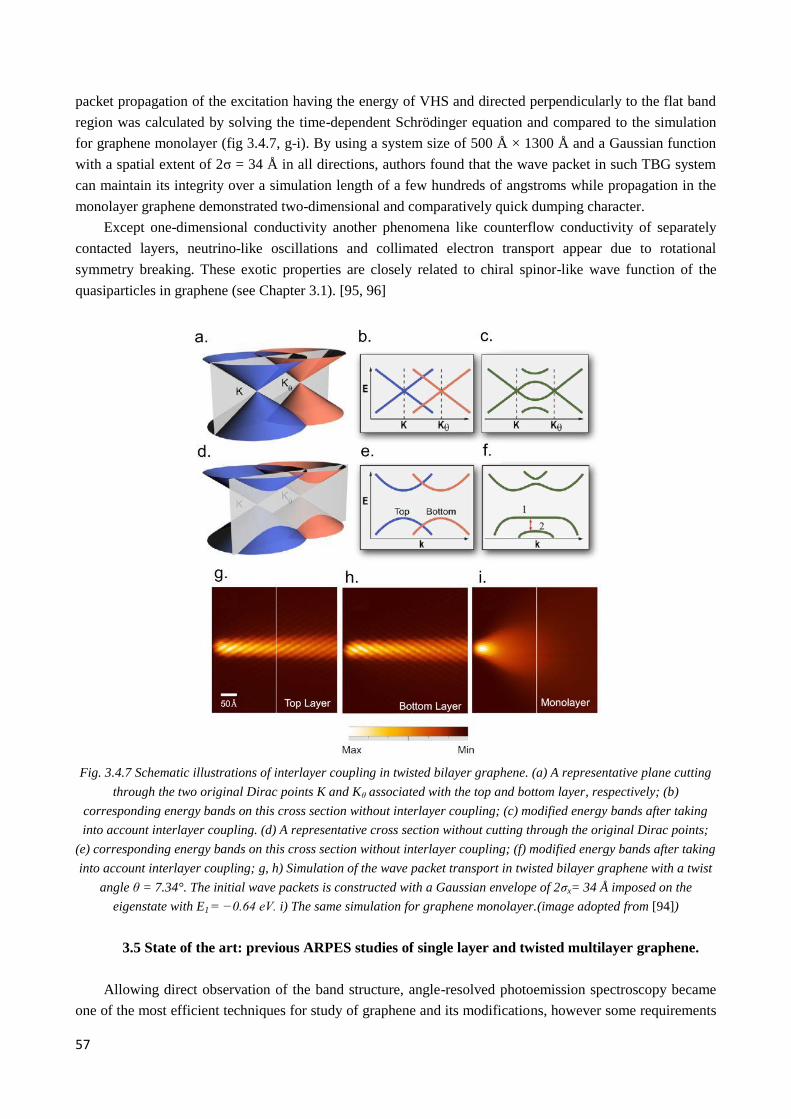
57
packet propagation of the excitation having the energy of VHS and directed perpendicularly to the flat band
region was calculated by solving the time-dependent Schrödinger equation and compared to the simulation
for graphene monolayer (fig 3.4.7, g-i). By using a system size of 500 Å × 1300 Å and a Gaussian function
with a spatial extent of 2σ = 34 Å in all directions, authors found that the wave packet in such TBG system
can maintain its integrity over a simulation length of a few hundreds of angstroms while propagation in the
monolayer graphene demonstrated two-dimensional and comparatively quick dumping character.
Except one-dimensional conductivity another phenomena like counterflow conductivity of separately
contacted layers, neutrino-like oscillations and collimated electron transport appear due to rotational
symmetry breaking. These exotic properties are closely related to chiral spinor-like wave function of the
quasiparticles in graphene (see Chapter 3.1). [95, 96]
Fig. 3.4.7 Schematic illustrations of interlayer coupling in twisted bilayer graphene. (a) A representative plane cutting
through the two original Dirac points K and Kθ associated with the top and bottom layer, respectively; (b)
corresponding energy bands on this cross section without interlayer coupling; (c) modified energy bands after taking
into account interlayer coupling. (d) A representative cross section without cutting through the original Dirac points;
(e) corresponding energy bands on this cross section without interlayer coupling; (f) modified energy bands after taking
into account interlayer coupling; g, h) Simulation of the wave packet transport in twisted bilayer graphene with a twist
angle θ = 7.34°. The initial wave packets is constructed with a Gaussian envelope of 2σx= 34 Å imposed on the
eigenstate with E1 = −0.64 eV. i) The same simulation for graphene monolayer.(image adopted from [94])
3.5 State of the art: previous ARPES studies of single layer and twisted multilayer graphene.
Allowing direct observation of the band structure, angle-resolved photoemission spectroscopy became
one of the most efficient techniques for study of graphene and its modifications, however some requirements
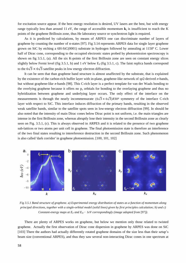
58
for excitation source appear. If the best energy resolution is desired, UV lasers are the best, but with energy
range typically less than around 11 eV, the range of accessible momentum k|| is insufficient to reach the K
points of the graphene Brillouin zone, thus He laboratory source or synchrotron light is required.
As it is predicted by calculations, by means of ARPES one can discriminate number of layers of
graphene by counting the number of π-states [97]. Fig 3.14 represents ARPES data for single layer graphene
grown on SiC by etching a 6H-SiC(0001) substrate in hydrogen followed by annealing at 1150º C. Lower
half of Dirac cone, corresponding to the occupied electronic states probed by photoemission spectroscopy is
shown on fig 3.5.1, (a). All the six K-points of the first Brillouin zone are seen on constant energy slices
slightly below Fermi level (fig 3.5.1, b) and 1 eV below EF (fig 3.5.1, c). The faint replica bands correspond
to the 6√3 × 6√3 satellite peaks in low energy electron diffraction.
It can be seen that than graphene band structure is almost unaffected by the substrate, that is explained
by the existence of the carbon-rich buffer layer with in-plane, graphene-like network of sp2-derived σ-bands,
but without graphene-like π-bands [98]. This C-rich layer is a perfect template for van der Waals bonding to
the overlying graphene because it offers no pz orbitals for bonding to the overlaying graphene and thus no
hybridization between graphene and underlying layer occurs. The only effect of the interface on the
measurements is through the nearly incommensurate (6√3 × 6√3)𝑅30º symmetry of the interface C-rich
layer with respect to SiC. This interface induces diffraction of the primary bands, resulting in the observed
weak satellite bands, similar to the satellite spots seen in low-energy electron diffraction [99]. In should be
also noted that the intensity of main Dirac cones below Dirac point is not uniform, i.e. the main triangles are
intense in the first Brillouin zone, whereas abruptly lose their intensity in the second Brillouin zone as clearly
seen on Fig. 3.5.1, (c). This is always observed in ARPES and it is related to the presence of two graphene
sub-lattices or two atoms per unit cell in graphene. The final photoemission state is therefore an interference
of the two final states resulting to intereference destruction in the second Brillouin zone. Such phenomenon
is also called 'dark corridor' in graphene photoemission. [100, 101, 102]
Fig 3.5.1 Band structure of graphene. a) Experimental energy distribution of states as a function of momentum along
principal directions, together with a single-orbital model (solid lines) given by first principles calculation; b) and c)
Constant-energy maps at EF and ED − 1eV correspondingly (image adopted from [97]).
There are plenty of ARPES works on graphene, but below we mention only those related to twisted
graphene. Actually the first observation of Dirac cone dispersion in graphene by ARPES was done on SiC
[103] There the authors had actually differently rotated graphene domains of the size less than their setup’s
beam size (conventional ARPES), and thus they saw several non-interacting Dirac cones in one spectrum at
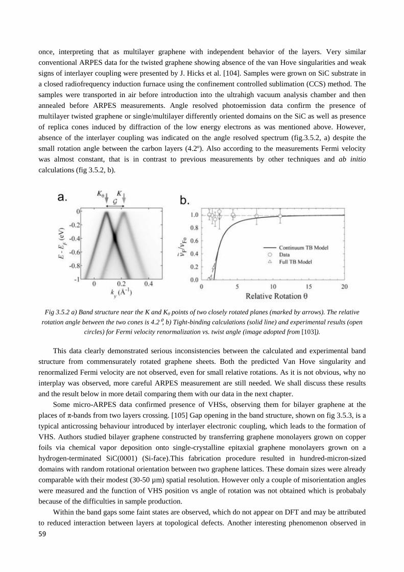
59
once, interpreting that as multilayer graphene with independent behavior of the layers. Very similar
conventional ARPES data for the twisted graphene showing absence of the van Hove singularities and weak
signs of interlayer coupling were presented by J. Hicks et al. [104]. Samples were grown on SiC substrate in
a closed radiofrequency induction furnace using the confinement controlled sublimation (CCS) method. The
samples were transported in air before introduction into the ultrahigh vacuum analysis chamber and then
annealed before ARPES measurements. Angle resolved photoemission data confirm the presence of
multilayer twisted graphene or single/multilayer differently oriented domains on the SiC as well as presence
of replica cones induced by diffraction of the low energy electrons as was mentioned above. However,
absence of the interlayer coupling was indicated on the angle resolved spectrum (fig.3.5.2, a) despite the
small rotation angle between the carbon layers (4.2º). Also according to the measurements Fermi velocity
was almost constant, that is in contrast to previous measurements by other techniques and ab initio
calculations (fig 3.5.2, b).
Fig 3.5.2 a) Band structure near the K and Kθ points of two closely rotated planes (marked by arrows). The relative
rotation angle between the two cones is 4.2⁰, b) Tight-binding calculations (solid line) and experimental results (open
circles) for Fermi velocity renormalization vs. twist angle (image adopted from [103]).
This data clearly demonstrated serious inconsistencies between the calculated and experimental band
structure from commensurately rotated graphene sheets. Both the predicted Van Hove singularity and
renormalized Fermi velocity are not observed, even for small relative rotations. As it is not obvious, why no
interplay was observed, more careful ARPES measurement are still needed. We shall discuss these results
and the result below in more detail comparing them with our data in the next chapter.
Some micro-ARPES data confirmed presence of VHSs, observing them for bilayer graphene at the
places of π-bands from two layers crossing. [105] Gap opening in the band structure, shown on fig 3.5.3, is a
typical anticrossing behaviour introduced by interlayer electronic coupling, which leads to the formation of
VHS. Authors studied bilayer graphene constructed by transferring graphene monolayers grown on copper
foils via chemical vapor deposition onto single-crystalline epitaxial graphene monolayers grown on a
hydrogen-terminated SiC(0001) (Si-face).This fabrication procedure resulted in hundred-micron-sized
domains with random rotational orientation between two graphene lattices. These domain sizes were already
comparable with their modest (30-50 µm) spatial resolution. However only a couple of misorientation angles
were measured and the function of VHS position vs angle of rotation was not obtained which is probabaly
because of the difficulties in sample production.
Within the band gaps some faint states are observed, which do not appear on DFT and may be attributed
to reduced interaction between layers at topological defects. Another interesting phenomenon observed in
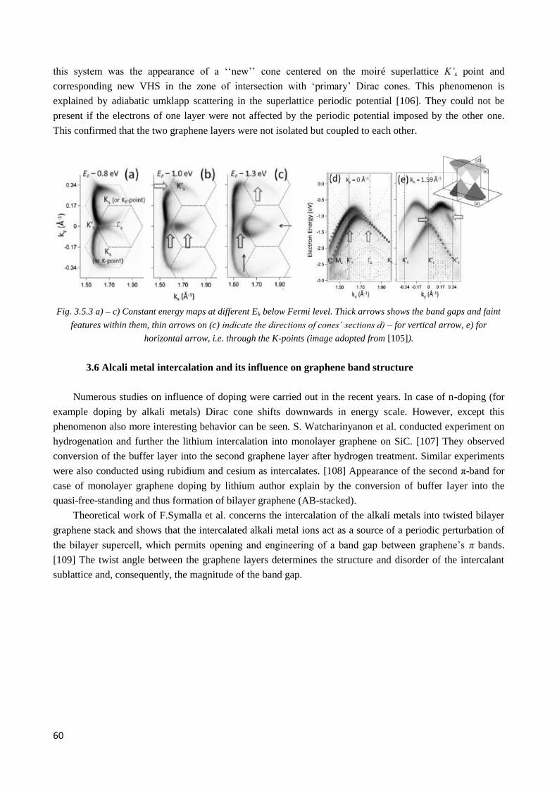
60
this system was the appearance of a ‘‘new’’ cone centered on the moiré superlattice K’s point and
corresponding new VHS in the zone of intersection with ‘primary’ Dirac cones. This phenomenon is
explained by adiabatic umklapp scattering in the superlattice periodic potential [106]. They could not be
present if the electrons of one layer were not affected by the periodic potential imposed by the other one.
This confirmed that the two graphene layers were not isolated but coupled to each other.
Fig. 3.5.3 a) – c) Constant energy maps at different Ek below Fermi level. Thick arrows shows the band gaps and faint
features within them, thin arrows on (c) indicate the directions of cones’ sections d) – for vertical arrow, e) for
horizontal arrow, i.e. through the K-points (image adopted from [105]).
3.6 Alcali metal intercalation and its influence on graphene band structure
Numerous studies on influence of doping were carried out in the recent years. In case of n-doping (for
example doping by alkali metals) Dirac cone shifts downwards in energy scale. However, except this
phenomenon also more interesting behavior can be seen. S. Watcharinyanon et al. conducted experiment on
hydrogenation and further the lithium intercalation into monolayer graphene on SiC. [107] They observed
conversion of the buffer layer into the second graphene layer after hydrogen treatment. Similar experiments
were also conducted using rubidium and cesium as intercalates. [108] Appearance of the second π-band for
case of monolayer graphene doping by lithium author explain by the conversion of buffer layer into the
quasi-free-standing and thus formation of bilayer graphene (AB-stacked).
Theoretical work of F.Symalla et al. concerns the intercalation of the alkali metals into twisted bilayer
graphene stack and shows that the intercalated alkali metal ions act as a source of a periodic perturbation of
the bilayer supercell, which permits opening and engineering of a band gap between graphene’s π bands.
[109] The twist angle between the graphene layers determines the structure and disorder of the intercalant
sublattice and, consequently, the magnitude of the band gap.
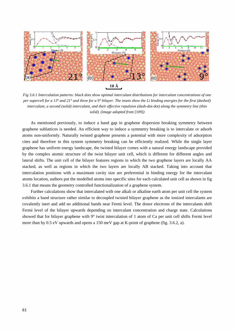
61
Fig 3.6.1 Intercalation patterns: black dots show optimal intercalant distributions for intercalant concentrations of one
per supercell for a 13º and 21° and three for a 9° bilayer. The insets show the Li binding energies for the first (dashed)
intercalant, a second (solid) intercalant, and their effective repulsion (dash-dot-dot) along the symmetry line (thin
solid). (image adopted from [109])
As mentioned previously, to induce a band gap in graphene dispersion breaking symmetry between
graphene sublattices is needed. An efficient way to induce a symmetry breaking is to intercalate or adsorb
atoms non-uniformly. Naturally twisted graphene presents a potential with more complexity of adsorption
cites and therefore in this system symmetry breaking can be efficiently realized. While the single layer
graphene has uniform energy landscape, the twisted bilayer comes with a natural energy landscape provided
by the complex atomic structure of the twist bilayer unit cell, which is different for different angles and
lateral shifts. The unit cell of the bilayer features regions in which the two graphene layers are locally AA
stacked, as well as regions in which the two layers are locally AB stacked. Taking into account that
intercalation positions with a maximum cavity size are preferential in binding energy for the intercalant
atoms location, authors put the modelled atoms into specific sites for each calculated unit cell as shown in fig
3.6.1 that means the geometry controlled functionalization of a graphene system.
Further calculations show that intercalated with one alkali or alkaline earth atom per unit cell the system
exhibits a band structure rather similar to decoupled twisted bilayer graphene as the ionized intercalants are
covalently inert and add no additional bands near Fermi level. The donor electrons of the intercalants shift
Fermi level of the bilayer upwards depending on intercalant concentration and charge state. Calculations
showed that for bilayer graphene with 9° twist intercalation of 1 atom of Ca per unit cell shifts Fermi level
more than by 0.5 eV upwards and opens a 150 meV gap at K-point of graphene (fig. 3.6.2, a).
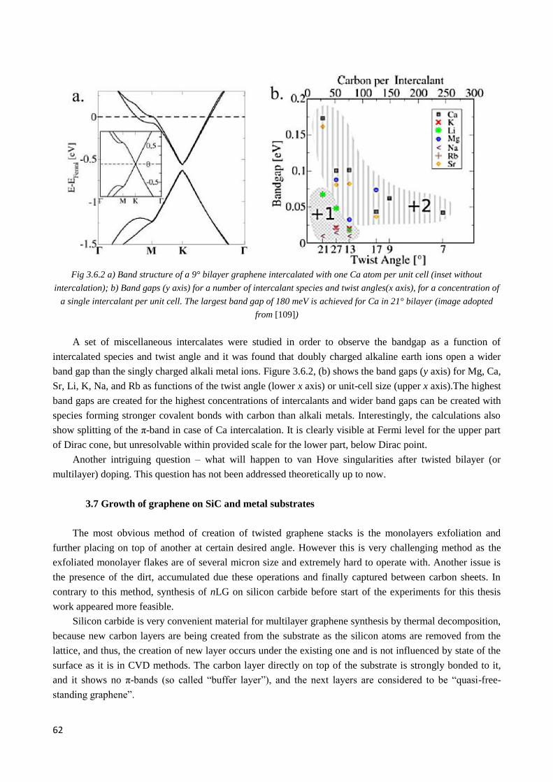
62
Fig 3.6.2 a) Band structure of a 9° bilayer graphene intercalated with one Ca atom per unit cell (inset without
intercalation); b) Band gaps (y axis) for a number of intercalant species and twist angles(x axis), for a concentration of
a single intercalant per unit cell. The largest band gap of 180 meV is achieved for Ca in 21° bilayer (image adopted
from [109])
A set of miscellaneous intercalates were studied in order to observe the bandgap as a function of
intercalated species and twist angle and it was found that doubly charged alkaline earth ions open a wider
band gap than the singly charged alkali metal ions. Figure 3.6.2, (b) shows the band gaps (y axis) for Mg, Ca,
Sr, Li, K, Na, and Rb as functions of the twist angle (lower x axis) or unit-cell size (upper x axis).The highest
band gaps are created for the highest concentrations of intercalants and wider band gaps can be created with
species forming stronger covalent bonds with carbon than alkali metals. Interestingly, the calculations also
show splitting of the π-band in case of Ca intercalation. It is clearly visible at Fermi level for the upper part
of Dirac cone, but unresolvable within provided scale for the lower part, below Dirac point.
Another intriguing question – what will happen to van Hove singularities after twisted bilayer (or
multilayer) doping. This question has not been addressed theoretically up to now.
3.7 Growth of graphene on SiC and metal substrates
The most obvious method of creation of twisted graphene stacks is the monolayers exfoliation and
further placing on top of another at certain desired angle. However this is very challenging method as the
exfoliated monolayer flakes are of several micron size and extremely hard to operate with. Another issue is
the presence of the dirt, accumulated due these operations and finally captured between carbon sheets. In
contrary to this method, synthesis of nLG on silicon carbide before start of the experiments for this thesis
work appeared more feasible.
Silicon carbide is very convenient material for multilayer graphene synthesis by thermal decomposition,
because new carbon layers are being created from the substrate as the silicon atoms are removed from the
lattice, and thus, the creation of new layer occurs under the existing one and is not influenced by state of the
surface as it is in CVD methods. The carbon layer directly on top of the substrate is strongly bonded to it,
and it shows no π-bands (so called “buffer layer”), and the next layers are considered to be “quasi-free-
standing graphene”.
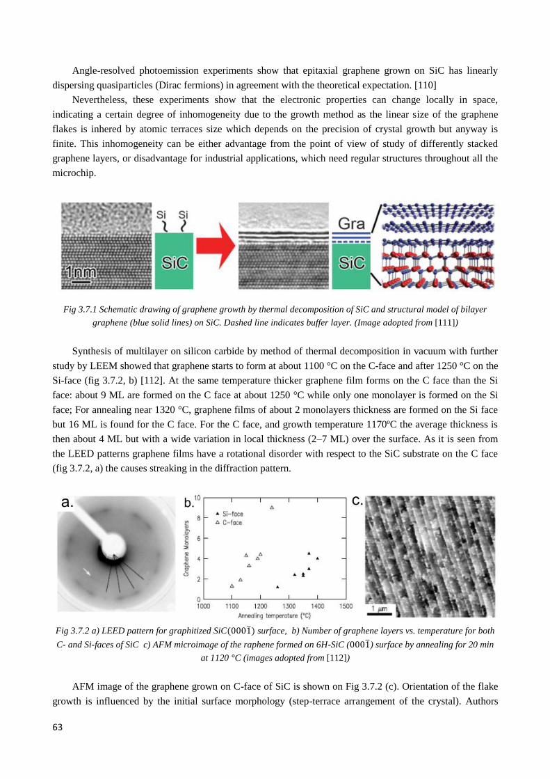
63
Angle-resolved photoemission experiments show that epitaxial graphene grown on SiC has linearly
dispersing quasiparticles (Dirac fermions) in agreement with the theoretical expectation. [110]
Nevertheless, these experiments show that the electronic properties can change locally in space,
indicating a certain degree of inhomogeneity due to the growth method as the linear size of the graphene
flakes is inhered by atomic terraces size which depends on the precision of crystal growth but anyway is
finite. This inhomogeneity can be either advantage from the point of view of study of differently stacked
graphene layers, or disadvantage for industrial applications, which need regular structures throughout all the
microchip.
Fig 3.7.1 Schematic drawing of graphene growth by thermal decomposition of SiC and structural model of bilayer
graphene (blue solid lines) on SiC. Dashed line indicates buffer layer. (Image adopted from [111])
Synthesis of multilayer on silicon carbide by method of thermal decomposition in vacuum with further
study by LEEM showed that graphene starts to form at about 1100 °C on the C-face and after 1250 °C on the
Si-face (fig 3.7.2, b) [112]. At the same temperature thicker graphene film forms on the C face than the Si
face: about 9 ML are formed on the C face at about 1250 °C while only one monolayer is formed on the Si
face; For annealing near 1320 °C, graphene films of about 2 monolayers thickness are formed on the Si face
but 16 ML is found for the C face. For the C face, and growth temperature 1170ºC the average thickness is
then about 4 ML but with a wide variation in local thickness (2–7 ML) over the surface. As it is seen from
the LEED patterns graphene films have a rotational disorder with respect to the SiC substrate on the C face
(fig 3.7.2, a) the causes streaking in the diffraction pattern.
Fig 3.7.2 a) LEED pattern for graphitized SiC(0001) surface, b) Number of graphene layers vs. temperature for both
C- and Si-faces of SiC c) AFM microimage of the raphene formed on 6H-SiC (0001) surface by annealing for 20 min
at 1120 °C (images adopted from [112])
AFM image of the graphene grown on C-face of SiC is shown on Fig 3.7.2 (c). Orientation of the flake
growth is influenced by the initial surface morphology (step-terrace arrangement of the crystal). Authors
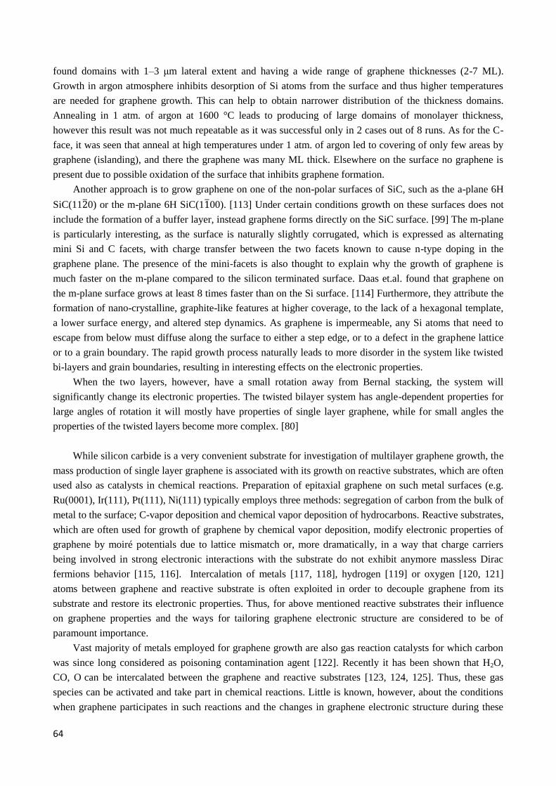
64
found domains with 1–3 μm lateral extent and having a wide range of graphene thicknesses (2-7 ML).
Growth in argon atmosphere inhibits desorption of Si atoms from the surface and thus higher temperatures
are needed for graphene growth. This can help to obtain narrower distribution of the thickness domains.
Annealing in 1 atm. of argon at 1600 °C leads to producing of large domains of monolayer thickness,
however this result was not much repeatable as it was successful only in 2 cases out of 8 runs. As for the C-
face, it was seen that anneal at high temperatures under 1 atm. of argon led to covering of only few areas by
graphene (islanding), and there the graphene was many ML thick. Elsewhere on the surface no graphene is
present due to possible oxidation of the surface that inhibits graphene formation.
Another approach is to grow graphene on one of the non-polar surfaces of SiC, such as the a-plane 6H
SiC(1120) or the m-plane 6H SiC(1100). [113] Under certain conditions growth on these surfaces does not
include the formation of a buffer layer, instead graphene forms directly on the SiC surface. [99] The m-plane
is particularly interesting, as the surface is naturally slightly corrugated, which is expressed as alternating
mini Si and C facets, with charge transfer between the two facets known to cause n-type doping in the
graphene plane. The presence of the mini-facets is also thought to explain why the growth of graphene is
much faster on the m-plane compared to the silicon terminated surface. Daas et.al. found that graphene on
the m-plane surface grows at least 8 times faster than on the Si surface. [114] Furthermore, they attribute the
formation of nano-crystalline, graphite-like features at higher coverage, to the lack of a hexagonal template,
a lower surface energy, and altered step dynamics. As graphene is impermeable, any Si atoms that need to
escape from below must diffuse along the surface to either a step edge, or to a defect in the graphene lattice
or to a grain boundary. The rapid growth process naturally leads to more disorder in the system like twisted
bi-layers and grain boundaries, resulting in interesting effects on the electronic properties.
When the two layers, however, have a small rotation away from Bernal stacking, the system will
significantly change its electronic properties. The twisted bilayer system has angle-dependent properties for
large angles of rotation it will mostly have properties of single layer graphene, while for small angles the
properties of the twisted layers become more complex. [80]
While silicon carbide is a very convenient substrate for investigation of multilayer graphene growth, the
mass production of single layer graphene is associated with its growth on reactive substrates, which are often
used also as catalysts in chemical reactions. Preparation of epitaxial graphene on such metal surfaces (e.g.
Ru(0001), Ir(111), Pt(111), Ni(111) typically employs three methods: segregation of carbon from the bulk of
metal to the surface; C-vapor deposition and chemical vapor deposition of hydrocarbons. Reactive substrates,
which are often used for growth of graphene by chemical vapor deposition, modify electronic properties of
graphene by moiré potentials due to lattice mismatch or, more dramatically, in a way that charge carriers
being involved in strong electronic interactions with the substrate do not exhibit anymore massless Dirac
fermions behavior [115, 116]. Intercalation of metals [117, 118], hydrogen [119] or oxygen [120, 121]
atoms between graphene and reactive substrate is often exploited in order to decouple graphene from its
substrate and restore its electronic properties. Thus, for above mentioned reactive substrates their influence
on graphene properties and the ways for tailoring graphene electronic structure are considered to be of
paramount importance.
Vast majority of metals employed for graphene growth are also gas reaction catalysts for which carbon
was since long considered as poisoning contamination agent [122]. Recently it has been shown that H2O,
CO, O can be intercalated between the graphene and reactive substrates [123, 124, 125]. Thus, these gas
species can be activated and take part in chemical reactions. Little is known, however, about the conditions
when graphene participates in such reactions and the changes in graphene electronic structure during these
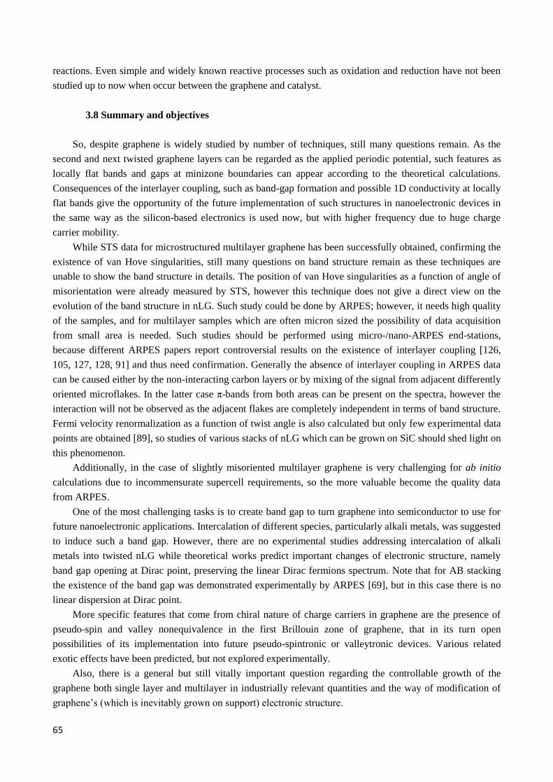
65
reactions. Even simple and widely known reactive processes such as oxidation and reduction have not been
studied up to now when occur between the graphene and catalyst.
3.8 Summary and objectives
So, despite graphene is widely studied by number of techniques, still many questions remain. As the
second and next twisted graphene layers can be regarded as the applied periodic potential, such features as
locally flat bands and gaps at minizone boundaries can appear according to the theoretical calculations.
Consequences of the interlayer coupling, such as band-gap formation and possible 1D conductivity at locally
flat bands give the opportunity of the future implementation of such structures in nanoelectronic devices in
the same way as the silicon-based electronics is used now, but with higher frequency due to huge charge
carrier mobility.
While STS data for microstructured multilayer graphene has been successfully obtained, confirming the
existence of van Hove singularities, still many questions on band structure remain as these techniques are
unable to show the band structure in details. The position of van Hove singularities as a function of angle of
misorientation were already measured by STS, however this technique does not give a direct view on the
evolution of the band structure in nLG. Such study could be done by ARPES; however, it needs high quality
of the samples, and for multilayer samples which are often micron sized the possibility of data acquisition
from small area is needed. Such studies should be performed using micro-/nano-ARPES end-stations,
because different ARPES papers report controversial results on the existence of interlayer coupling [126,
105, 127, 128, 91] and thus need confirmation. Generally the absence of interlayer coupling in ARPES data
can be caused either by the non-interacting carbon layers or by mixing of the signal from adjacent differently
oriented microflakes. In the latter case π-bands from both areas can be present on the spectra, however the
interaction will not be observed as the adjacent flakes are completely independent in terms of band structure.
Fermi velocity renormalization as a function of twist angle is also calculated but only few experimental data
points are obtained [89], so studies of various stacks of nLG which can be grown on SiC should shed light on
this phenomenon.
Additionally, in the case of slightly misoriented multilayer graphene is very challenging for ab initio
calculations due to incommensurate supercell requirements, so the more valuable become the quality data
from ARPES.
One of the most challenging tasks is to create band gap to turn graphene into semiconductor to use for
future nanoelectronic applications. Intercalation of different species, particularly alkali metals, was suggested
to induce such a band gap. However, there are no experimental studies addressing intercalation of alkali
metals into twisted nLG while theoretical works predict important changes of electronic structure, namely
band gap opening at Dirac point, preserving the linear Dirac fermions spectrum. Note that for AB stacking
the existence of the band gap was demonstrated experimentally by ARPES [69], but in this case there is no
linear dispersion at Dirac point.
More specific features that come from chiral nature of charge carriers in graphene are the presence of
pseudo-spin and valley nonequivalence in the first Brillouin zone of graphene, that in its turn open
possibilities of its implementation into future pseudo-spintronic or valleytronic devices. Various related
exotic effects have been predicted, but not explored experimentally.
Also, there is a general but still vitally important question regarding the controllable growth of the
graphene both single layer and multilayer in industrially relevant quantities and the way of modification of
graphene’s (which is inevitably grown on support) electronic structure.
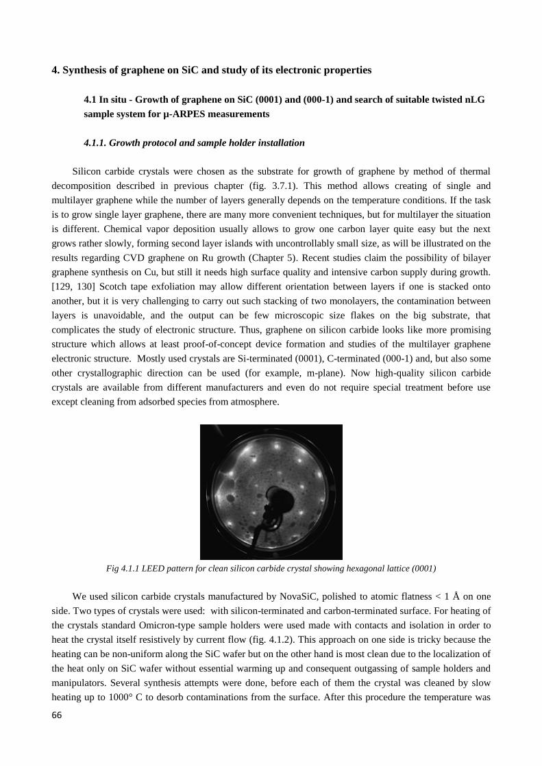
66
4. Synthesis of graphene on SiC and study of its electronic properties
4.1 In situ - Growth of graphene on SiC (0001) and (000-1) and search of suitable twisted nLG
sample system for µ-ARPES measurements
4.1.1. Growth protocol and sample holder installation
Silicon carbide crystals were chosen as the substrate for growth of graphene by method of thermal
decomposition described in previous chapter (fig. 3.7.1). This method allows creating of single and
multilayer graphene while the number of layers generally depends on the temperature conditions. If the task
is to grow single layer graphene, there are many more convenient techniques, but for multilayer the situation
is different. Chemical vapor deposition usually allows to grow one carbon layer quite easy but the next
grows rather slowly, forming second layer islands with uncontrollably small size, as will be illustrated on the
results regarding CVD graphene on Ru growth (Chapter 5). Recent studies claim the possibility of bilayer
graphene synthesis on Cu, but still it needs high surface quality and intensive carbon supply during growth.
[129, 130] Scotch tape exfoliation may allow different orientation between layers if one is stacked onto
another, but it is very challenging to carry out such stacking of two monolayers, the contamination between
layers is unavoidable, and the output can be few microscopic size flakes on the big substrate, that
complicates the study of electronic structure. Thus, graphene on silicon carbide looks like more promising
structure which allows at least proof-of-concept device formation and studies of the multilayer graphene
electronic structure. Mostly used crystals are Si-terminated (0001), C-terminated (000-1) and, but also some
other crystallographic direction can be used (for example, m-plane). Now high-quality silicon carbide
crystals are available from different manufacturers and even do not require special treatment before use
except cleaning from adsorbed species from atmosphere.
Fig 4.1.1 LEED pattern for clean silicon carbide crystal showing hexagonal lattice (0001)
We used silicon carbide crystals manufactured by NovaSiC, polished to atomic flatness < 1 Å on one
side. Two types of crystals were used: with silicon-terminated and carbon-terminated surface. For heating of
the crystals standard Omicron-type sample holders were used made with contacts and isolation in order to
heat the crystal itself resistively by current flow (fig. 4.1.2). This approach on one side is tricky because the
heating can be non-uniform along the SiC wafer but on the other hand is most clean due to the localization of
the heat only on SiC wafer without essential warming up and consequent outgassing of sample holders and
manipulators. Several synthesis attempts were done, before each of them the crystal was cleaned by slow
heating up to 1000° C to desorb contaminations from the surface. After this procedure the temperature was
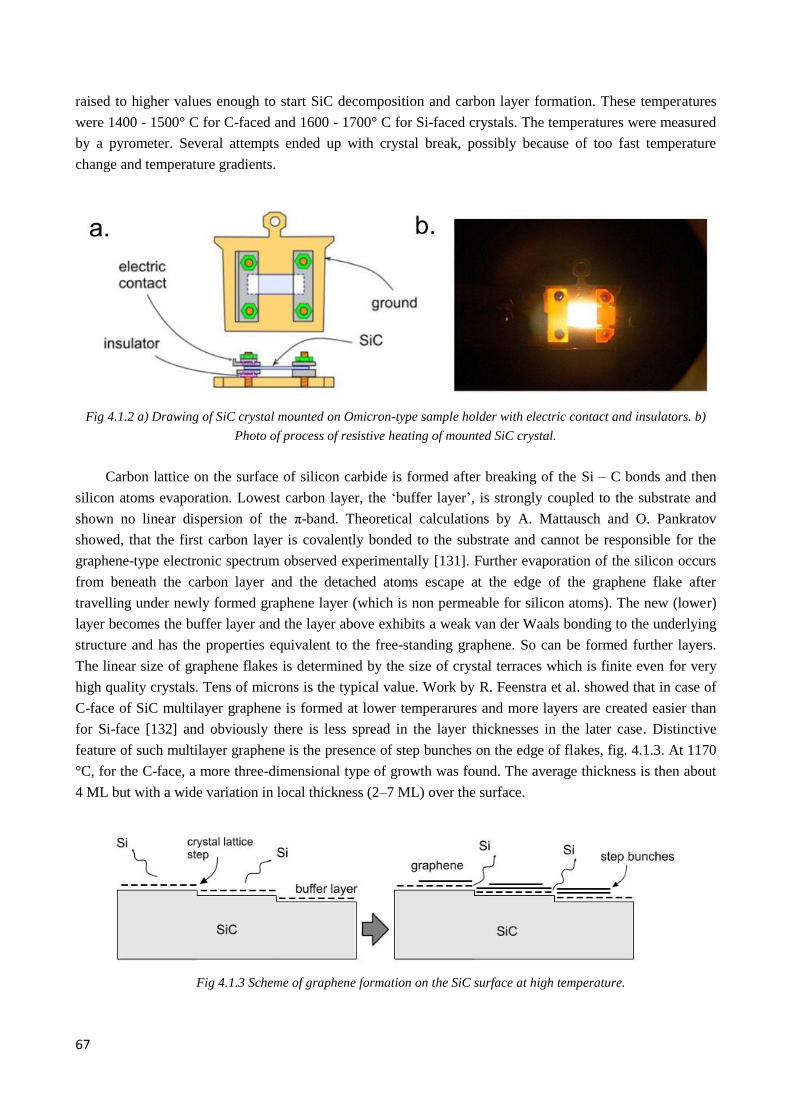
67
raised to higher values enough to start SiC decomposition and carbon layer formation. These temperatures
were 1400 - 1500° C for C-faced and 1600 - 1700° C for Si-faced crystals. The temperatures were measured
by a pyrometer. Several attempts ended up with crystal break, possibly because of too fast temperature
change and temperature gradients.
Fig 4.1.2 a) Drawing of SiC crystal mounted on Omicron-type sample holder with electric contact and insulators. b)
Photo of process of resistive heating of mounted SiC crystal.
Carbon lattice on the surface of silicon carbide is formed after breaking of the Si – C bonds and then
silicon atoms evaporation. Lowest carbon layer, the ‘buffer layer’, is strongly coupled to the substrate and
shown no linear dispersion of the π-band. Theoretical calculations by A. Mattausch and O. Pankratov
showed, that the first carbon layer is covalently bonded to the substrate and cannot be responsible for the
graphene-type electronic spectrum observed experimentally [131]. Further evaporation of the silicon occurs
from beneath the carbon layer and the detached atoms escape at the edge of the graphene flake after
travelling under newly formed graphene layer (which is non permeable for silicon atoms). The new (lower)
layer becomes the buffer layer and the layer above exhibits a weak van der Waals bonding to the underlying
structure and has the properties equivalent to the free-standing graphene. So can be formed further layers.
The linear size of graphene flakes is determined by the size of crystal terraces which is finite even for very
high quality crystals. Tens of microns is the typical value. Work by R. Feenstra et al. showed that in case of
C-face of SiC multilayer graphene is formed at lower temperarures and more layers are created easier than
for Si-face [132] and obviously there is less spread in the layer thicknesses in the later case. Distinctive
feature of such multilayer graphene is the presence of step bunches on the edge of flakes, fig. 4.1.3. At 1170
°C, for the C-face, a more three-dimensional type of growth was found. The average thickness is then about
4 ML but with a wide variation in local thickness (2–7 ML) over the surface.
Fig 4.1.3 Scheme of graphene formation on the SiC surface at high temperature.
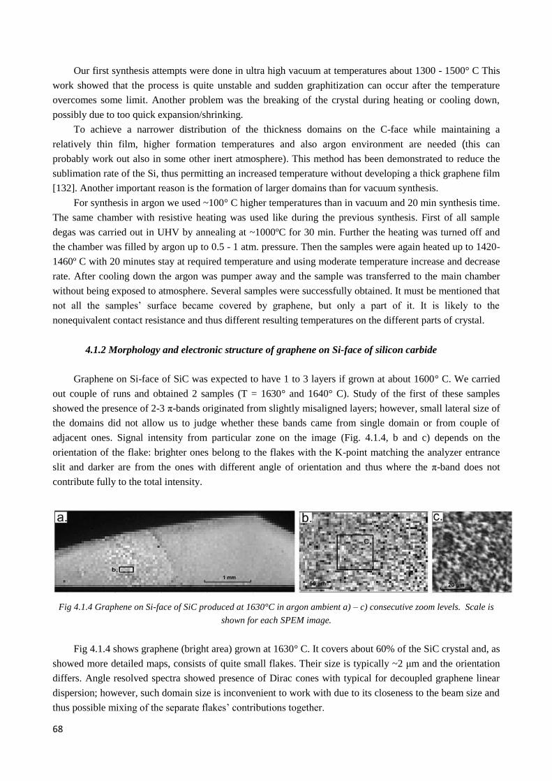
68
Our first synthesis attempts were done in ultra high vacuum at temperatures about 1300 - 1500° C This
work showed that the process is quite unstable and sudden graphitization can occur after the temperature
overcomes some limit. Another problem was the breaking of the crystal during heating or cooling down,
possibly due to too quick expansion/shrinking.
To achieve a narrower distribution of the thickness domains on the C-face while maintaining a
relatively thin film, higher formation temperatures and also argon environment are needed (this can
probably work out also in some other inert atmosphere). This method has been demonstrated to reduce the
sublimation rate of the Si, thus permitting an increased temperature without developing a thick graphene film
[132]. Another important reason is the formation of larger domains than for vacuum synthesis.
For synthesis in argon we used ~100° C higher temperatures than in vacuum and 20 min synthesis time.
The same chamber with resistive heating was used like during the previous synthesis. First of all sample
degas was carried out in UHV by annealing at ~1000ºC for 30 min. Further the heating was turned off and
the chamber was filled by argon up to 0.5 - 1 atm. pressure. Then the samples were again heated up to 1420-
1460º C with 20 minutes stay at required temperature and using moderate temperature increase and decrease
rate. After cooling down the argon was pumper away and the sample was transferred to the main chamber
without being exposed to atmosphere. Several samples were successfully obtained. It must be mentioned that
not all the samples’ surface became covered by graphene, but only a part of it. It is likely to the
nonequivalent contact resistance and thus different resulting temperatures on the different parts of crystal.
4.1.2 Morphology and electronic structure of graphene on Si-face of silicon carbide
Graphene on Si-face of SiC was expected to have 1 to 3 layers if grown at about 1600° C. We carried
out couple of runs and obtained 2 samples (T = 1630° and 1640° C). Study of the first of these samples
showed the presence of 2-3 π-bands originated from slightly misaligned layers; however, small lateral size of
the domains did not allow us to judge whether these bands came from single domain or from couple of
adjacent ones. Signal intensity from particular zone on the image (Fig. 4.1.4, b and c) depends on the
orientation of the flake: brighter ones belong to the flakes with the K-point matching the analyzer entrance
slit and darker are from the ones with different angle of orientation and thus where the π-band does not
contribute fully to the total intensity.
Fig 4.1.4 Graphene on Si-face of SiC produced at 1630°C in argon ambient a) – c) consecutive zoom levels. Scale is
shown for each SPEM image.
Fig 4.1.4 shows graphene (bright area) grown at 1630° C. It covers about 60% of the SiC crystal and, as
showed more detailed maps, consists of quite small flakes. Their size is typically ~2 μm and the orientation
differs. Angle resolved spectra showed presence of Dirac cones with typical for decoupled graphene linear
dispersion; however, such domain size is inconvenient to work with due to its closeness to the beam size and
thus possible mixing of the separate flakes’ contributions together.
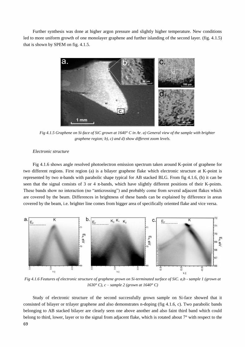
69
Further synthesis was done at higher argon pressure and slightly higher temperature. New conditions
led to more uniform growth of one monolayer graphene and further islanding of the second layer. (fig. 4.1.5)
that is shown by SPEM on fig. 4.1.5.
Fig 4.1.5 Graphene on Si-face of SiC grown at 1640° C in Ar. a) General view of the sample with brighter
graphene region; b), c) and d) show different zoom levels.
Electronic structure
Fig 4.1.6 shows angle resolved photoelectron emission spectrum taken around K-point of graphene for
two different regions. First region (a) is a bilayer graphene flake which electronic structure at K-point is
represented by two π-bands with parabolic shape typical for AB stacked BLG. From fig 4.1.6, (b) it can be
seen that the signal consists of 3 or 4 π-bands, which have slightly different positions of their K-points.
These bands show no interaction (no “anticrossing”) and probably come from several adjacent flakes which
are covered by the beam. Differences in brightness of these bands can be explained by difference in areas
covered by the beam, i.e. brighter line comes from bigger area of specifically oriented flake and vice versa.
Fig 4.1.6 Features of electronic structure of graphene grown on Si-terminated surface of SiC. a,b - sample 1 (grown at
1630° C), c – sample 2 (grown at 1640° C)
Study of electronic structure of the second successfully grown sample on Si-face showed that it
consisted of bilayer or trilayer graphene and also demonstrates n-doping (fig 4.1.6, c). Two parabolic bands
belonging to AB stacked bilayer are clearly seen one above another and also faint third band which could
belong to third, lower, layer or to the signal from adjacent flake, which is rotated about 7° with respect to the
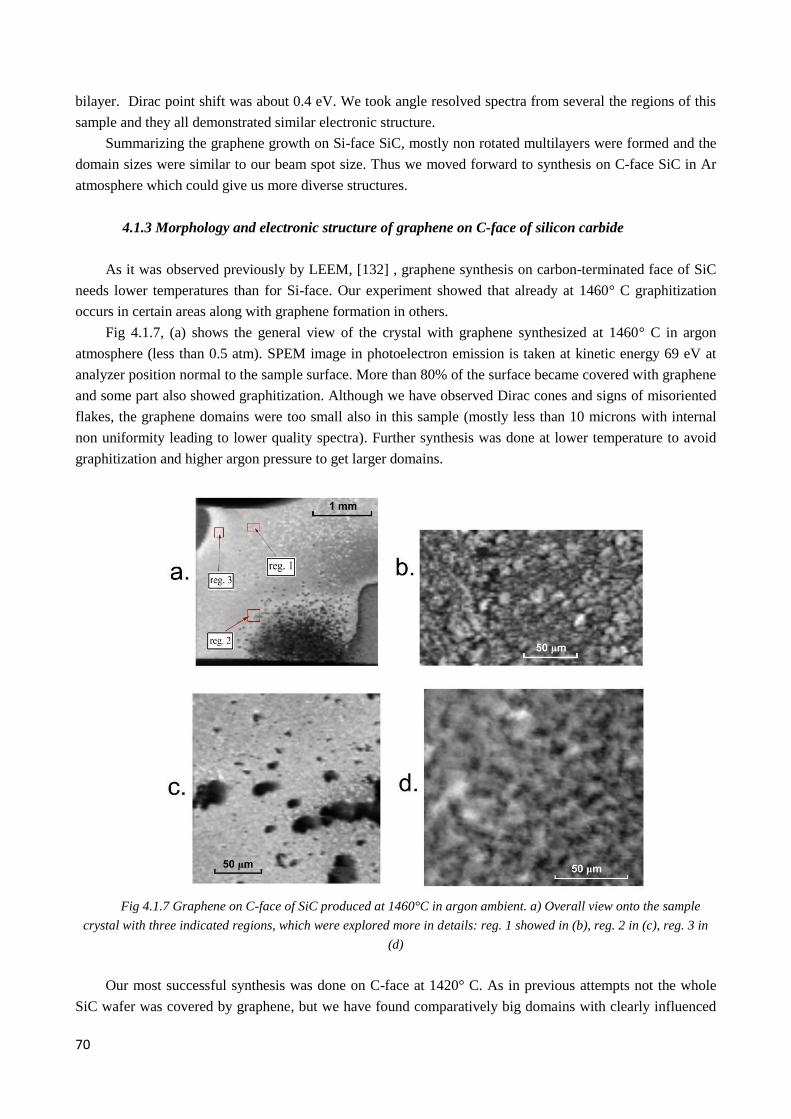
70
bilayer. Dirac point shift was about 0.4 eV. We took angle resolved spectra from several the regions of this
sample and they all demonstrated similar electronic structure.
Summarizing the graphene growth on Si-face SiC, mostly non rotated multilayers were formed and the
domain sizes were similar to our beam spot size. Thus we moved forward to synthesis on C-face SiC in Ar
atmosphere which could give us more diverse structures.
4.1.3 Morphology and electronic structure of graphene on C-face of silicon carbide
As it was observed previously by LEEM, [132] , graphene synthesis on carbon-terminated face of SiC
needs lower temperatures than for Si-face. Our experiment showed that already at 1460° C graphitization
occurs in certain areas along with graphene formation in others.
Fig 4.1.7, (a) shows the general view of the crystal with graphene synthesized at 1460° C in argon
atmosphere (less than 0.5 atm). SPEM image in photoelectron emission is taken at kinetic energy 69 eV at
analyzer position normal to the sample surface. More than 80% of the surface became covered with graphene
and some part also showed graphitization. Although we have observed Dirac cones and signs of misoriented
flakes, the graphene domains were too small also in this sample (mostly less than 10 microns with internal
non uniformity leading to lower quality spectra). Further synthesis was done at lower temperature to avoid
graphitization and higher argon pressure to get larger domains.
Fig 4.1.7 Graphene on C-face of SiC produced at 1460°C in argon ambient. a) Overall view onto the sample
crystal with three indicated regions, which were explored more in details: reg. 1 showed in (b), reg. 2 in (c), reg. 3 in
(d)
Our most successful synthesis was done on C-face at 1420° C. As in previous attempts not the whole
SiC wafer was covered by graphene, but we have found comparatively big domains with clearly influenced
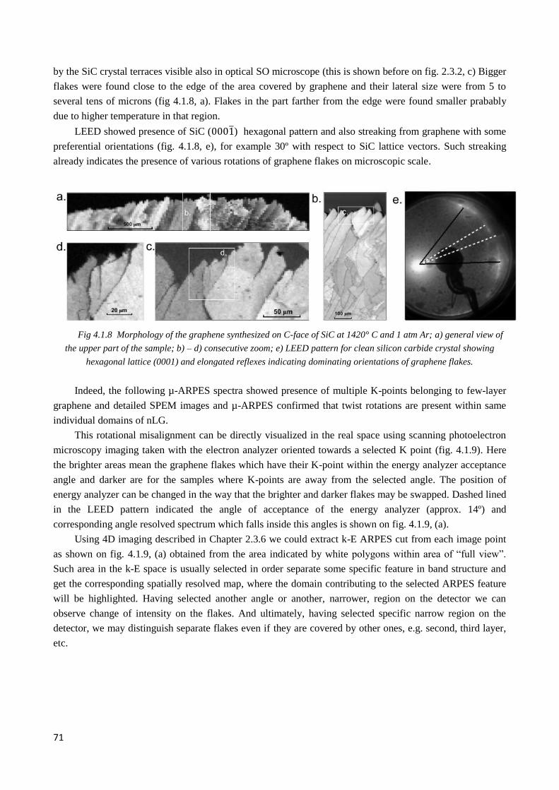
71
by the SiC crystal terraces visible also in optical SO microscope (this is shown before on fig. 2.3.2, c) Bigger
flakes were found close to the edge of the area covered by graphene and their lateral size were from 5 to
several tens of microns (fig 4.1.8, a). Flakes in the part farther from the edge were found smaller prabably
due to higher temperature in that region.
LEED showed presence of SiC (0001) hexagonal pattern and also streaking from graphene with some
preferential orientations (fig. 4.1.8, e), for example 30º with respect to SiC lattice vectors. Such streaking
already indicates the presence of various rotations of graphene flakes on microscopic scale.
Fig 4.1.8 Morphology of the graphene synthesized on C-face of SiC at 1420° C and 1 atm Ar; a) general view of
the upper part of the sample; b) – d) consecutive zoom; e) LEED pattern for clean silicon carbide crystal showing
hexagonal lattice (0001) and elongated reflexes indicating dominating orientations of graphene flakes.
Indeed, the following µ-ARPES spectra showed presence of multiple K-points belonging to few-layer
graphene and detailed SPEM images and µ-ARPES confirmed that twist rotations are present within same
individual domains of nLG.
This rotational misalignment can be directly visualized in the real space using scanning photoelectron
microscopy imaging taken with the electron analyzer oriented towards a selected K point (fig. 4.1.9). Here
the brighter areas mean the graphene flakes which have their K-point within the energy analyzer acceptance
angle and darker are for the samples where K-points are away from the selected angle. The position of
energy analyzer can be changed in the way that the brighter and darker flakes may be swapped. Dashed lined
in the LEED pattern indicated the angle of acceptance of the energy analyzer (approx. 14º) and
corresponding angle resolved spectrum which falls inside this angles is shown on fig. 4.1.9, (a).
Using 4D imaging described in Chapter 2.3.6 we could extract k-E ARPES cut from each image point
as shown on fig. 4.1.9, (a) obtained from the area indicated by white polygons within area of “full view”.
Such area in the k-E space is usually selected in order separate some specific feature in band structure and
get the corresponding spatially resolved map, where the domain contributing to the selected ARPES feature
will be highlighted. Having selected another angle or another, narrower, region on the detector we can
observe change of intensity on the flakes. And ultimately, having selected specific narrow region on the
detector, we may distinguish separate flakes even if they are covered by other ones, e.g. second, third layer,
etc.
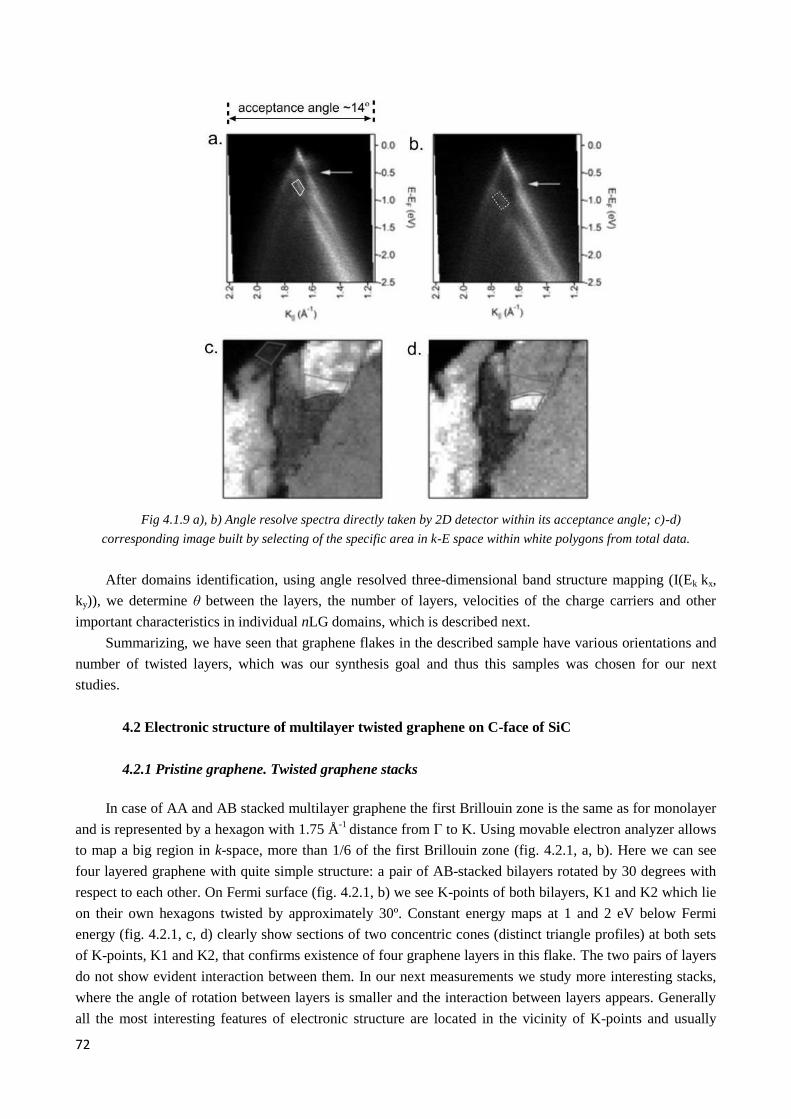
72
Fig 4.1.9 a), b) Angle resolve spectra directly taken by 2D detector within its acceptance angle; c)-d)
corresponding image built by selecting of the specific area in k-E space within white polygons from total data.
After domains identification, using angle resolved three-dimensional band structure mapping (I(Ek kx,
ky)), we determine θ between the layers, the number of layers, velocities of the charge carriers and other
important characteristics in individual nLG domains, which is described next.
Summarizing, we have seen that graphene flakes in the described sample have various orientations and
number of twisted layers, which was our synthesis goal and thus this samples was chosen for our next
studies.
4.2 Electronic structure of multilayer twisted graphene on C-face of SiC
4.2.1 Pristine graphene. Twisted graphene stacks
In case of AA and AB stacked multilayer graphene the first Brillouin zone is the same as for monolayer
and is represented by a hexagon with 1.75 Å-1
distance from Г to K. Using movable electron analyzer allows
to map a big region in k-space, more than 1/6 of the first Brillouin zone (fig. 4.2.1, a, b). Here we can see
four layered graphene with quite simple structure: a pair of AB-stacked bilayers rotated by 30 degrees with
respect to each other. On Fermi surface (fig. 4.2.1, b) we see K-points of both bilayers, K1 and K2 which lie
on their own hexagons twisted by approximately 30º. Constant energy maps at 1 and 2 eV below Fermi
energy (fig. 4.2.1, c, d) clearly show sections of two concentric cones (distinct triangle profiles) at both sets
of K-points, K1 and K2, that confirms existence of four graphene layers in this flake. The two pairs of layers
do not show evident interaction between them. In our next measurements we study more interesting stacks,
where the angle of rotation between layers is smaller and the interaction between layers appears. Generally
all the most interesting features of electronic structure are located in the vicinity of K-points and usually
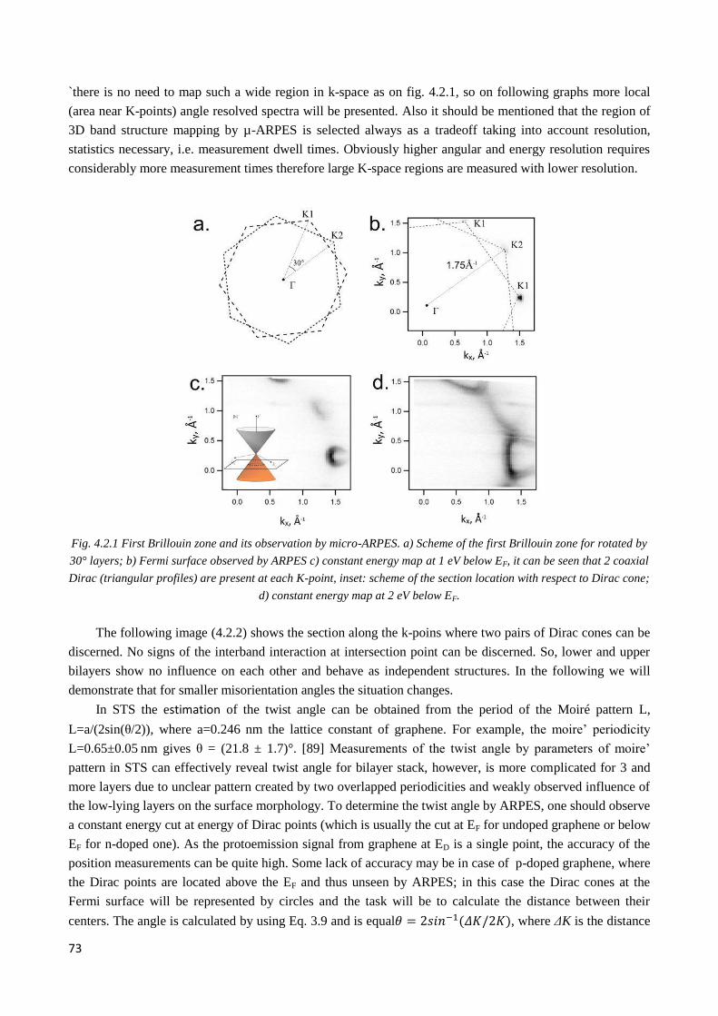
73
`there is no need to map such a wide region in k-space as on fig. 4.2.1, so on following graphs more local
(area near K-points) angle resolved spectra will be presented. Also it should be mentioned that the region of
3D band structure mapping by µ-ARPES is selected always as a tradeoff taking into account resolution,
statistics necessary, i.e. measurement dwell times. Obviously higher angular and energy resolution requires
considerably more measurement times therefore large K-space regions are measured with lower resolution.
Fig. 4.2.1 First Brillouin zone and its observation by micro-ARPES. a) Scheme of the first Brillouin zone for rotated by
30° layers; b) Fermi surface observed by ARPES c) constant energy map at 1 eV below EF, it can be seen that 2 coaxial
Dirac (triangular profiles) are present at each K-point, inset: scheme of the section location with respect to Dirac cone;
d) constant energy map at 2 eV below EF.
The following image (4.2.2) shows the section along the k-poins where two pairs of Dirac cones can be
discerned. No signs of the interband interaction at intersection point can be discerned. So, lower and upper
bilayers show no influence on each other and behave as independent structures. In the following we will
demonstrate that for smaller misorientation angles the situation changes.
In STS the estimation of the twist angle can be obtained from the period of the Moiré pattern L,
L=a/(2sin(θ/2)), where a=0.246 nm the lattice constant of graphene. For example, the moire’ periodicity
L=0.65±0.05 nm gives θ = (21.8 ± 1.7)°. [89] Measurements of the twist angle by parameters of moire’
pattern in STS can effectively reveal twist angle for bilayer stack, however, is more complicated for 3 and
more layers due to unclear pattern created by two overlapped periodicities and weakly observed influence of
the low-lying layers on the surface morphology. To determine the twist angle by ARPES, one should observe
a constant energy cut at energy of Dirac points (which is usually the cut at EF for undoped graphene or below
EF for n-doped one). As the protoemission signal from graphene at ED is a single point, the accuracy of the
position measurements can be quite high. Some lack of accuracy may be in case of p-doped graphene, where
the Dirac points are located above the EF and thus unseen by ARPES; in this case the Dirac cones at the
Fermi surface will be represented by circles and the task will be to calculate the distance between their
centers. The angle is calculated by using Eq. 3.9 and is equal𝜃 = 2𝑠𝑖𝑛−1(𝛥𝐾/2𝐾), where ΔK is the distance

74
between the K-points of different layers in k-space and K is the Γ-K distance (~1,75 Å-1
). With ARPES one
can easily discern contributions from 3-4 carbon layers, then to calculate the distance in k-space between
corresponding K-points and thus the twist angles.
Fig 4.2.2 Constant energy map at E = EF – 1 eV, dashed arrow line indicated the direction of the cut along K-points of
lower and upper layers. b) Cut along K-points. Thin solid lines indicate Fermi energy and energy at 1 eV below EF,
where section on the (a) is taken.
4.2.2 Observation of twisted graphene minizone. Odd and even type superlattices
As was described earlier in the Chapter 3.4, the displaced Dirac cones of the twisted bilayer cross, and
two intersections of the saddle points along the two cones appear in the presence of interlayer coupling. The
saddle points result in two low-energy van Hove singularities in the density of states (DOS), above and
below EF. Beside the VHSs, superlattice Dirac points emerge in the twisted graphene bilayer. When two
graphene layers are not isolated but sense each other, the graphene-on-graphene moiré pattern gives rise to a
periodic electronic potential of triangular symmetry. This periodic potential leads to the emergence of
superlattice Dirac points.
Fig. 4.2.3 a) Brillouin zones of two slightly rotated graphene layers; b) common minizone with its own high
symmetry points.
In slightly twisted multilayer graphene large real space superlattice formed by a pair of layers and can
be transformed into a minizone with its own K’-points (fig. 4.2.3). They also can be directly observed on
angle resolved spectra (fig. 4.2.4, b, c, e, f). The length of the minizone base vector depends on the distance
between main K-points Δk, e.g. on the rotation angle. The lesser angle is, the smaller minizone will be as
clearly demonstrated on the experimental angle resolved spectra taken from two bilayer graphene flakes with
different angle of misorientation (figs. 4.2.4, c, f). Here the first case has smaller angle and K’ points are
closer to the main K-points and vice versa. On angle resolved photoemission spectra we can directly observe
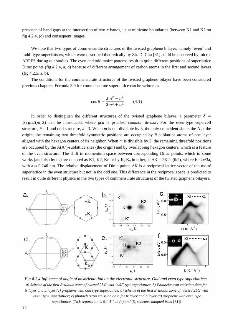
75
presence of band gaps at the intersection of two π-bands, i.e at minizone boundaries (between K1 and K2 on
fig 4.2.4, (c) and consequent images.
We note that two types of commensurate structures of the twisted graphene bilayer, namely ‘even’ and
‘odd’ type superlattices, which were described theoretically by Zh.-D. Chu [81] could be observed by micro-
ARPES during our studies. The even and odd moiré patterns result in quite different positions of superlattice
Dirac points (fig.4.2.4, a, d) because of different arrangement of carbon atoms in the first and second layers
(fig 4.2.5, a, b).
The conditions for the commensurate structures of the twisted graphene bilayer have been considered
previous chapters. Formula 3.9 for commensurate superlattice can be written as
cos 𝜃 =3𝑚2 − 𝑛2
3𝑚2 + 𝑛2 (4.1)
In order to distinguish the different structures of the twisted graphene bilayer, a parameter 𝛿 =
3/𝑔𝑐𝑑(𝑚, 3) can be introduced, where gcd is greatest common divisor. For the even-type supercell
structure, δ = 1 and odd structure, δ =3. When m is not divisible by 3, the only coincident site is the A at the
origin; the remaining two threefold-symmetric positions are occupied by B-sublattice atoms of one layer
aligned with the hexagon centers of its neighbor. When m is divisible by 3, the remaining threefold positions
are occupied by the A(A’)-sublattice sites (the origin) and by overlapping hexagon centers, which is a feature
of the even structure. The shift in momentum space between corresponding Dirac points, which in some
works (and also by us) are denoted as K1, K2, Kn or by K, Kθ in other, is ΔK = 2Ksin(θ/2), where K=4π/3a,
with a ≈ 0.246 nm. The relative displacement of Dirac points ΔK is a reciprocal lattice vector of the moiré
superlattice in the even structure but not in the odd one. This difference in the reciprocal space is predicted to
result in quite different physics in the two types of commensurate structures of the twisted graphene bilayers.
Fig 4.2.4 Influence of angle of misorientation on the electronic structure. Odd and even type superlattices.
a) Scheme of the first Brillouin zone of twisted 2LG with ‘odd’ type superlattice. b) Photoelectron emission data for
trilayer and bilayer (c) graphene with odd type superlattice; d) scheme of the first Brillouin zone of twisted 2LG with
‘even’ type superlattice; e) photoelectron emission data for trilayer and bilayer (c) graphene with even type
superlattice. (Tick separation is 0.1 Å−1
in (c) and (f), schemes adopted from [81])
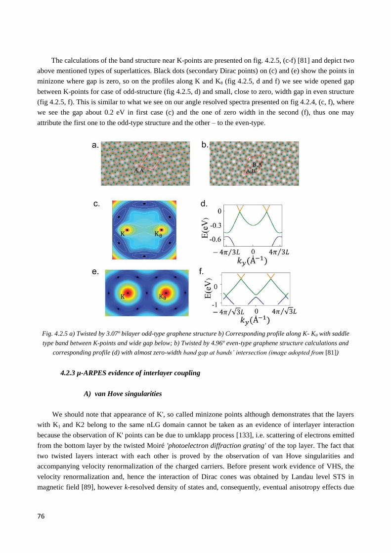
76
The calculations of the band structure near K-points are presented on fig. 4.2.5, (c-f) [81] and depict two
above mentioned types of superlattices. Black dots (secondary Dirac points) on (c) and (e) show the points in
minizone where gap is zero, so on the profiles along K and Kθ (fig 4.2.5, d and f) we see wide opened gap
between K-points for case of odd-structure (fig 4.2.5, d) and small, close to zero, width gap in even structure
(fig 4.2.5, f). This is similar to what we see on our angle resolved spectra presented on fig 4.2.4, (c, f), where
we see the gap about 0.2 eV in first case (c) and the one of zero width in the second (f), thus one may
attribute the first one to the odd-type structure and the other – to the even-type.
Fig. 4.2.5 a) Twisted by 3.07º bilayer odd-type graphene structure b) Corresponding profile along K- Kθ with saddle
type band between K-points and wide gap below; b) Twisted by 4.96º even-type graphene structure calculations and
corresponding profile (d) with almost zero-width band gap at bands’ intersection (image adopted from [81])
4.2.3 µ-ARPES evidence of interlayer coupling
A) van Hove singularities
We should note that appearance of K', so called minizone points although demonstrates that the layers
with K1 and K2 belong to the same nLG domain cannot be taken as an evidence of interlayer interaction
because the observation of K' points can be due to umklapp process [133], i.e. scattering of electrons emitted
from the bottom layer by the twisted Moiré 'photoelectron diffraction grating' of the top layer. The fact that
two twisted layers interact with each other is proved by the observation of van Hove singularities and
accompanying velocity renormalization of the charged carriers. Before present work evidence of VHS, the
velocity renormalization and, hence the interaction of Dirac cones was obtained by Landau level STS in
magnetic field [89], however k-resolved density of states and, consequently, eventual anisotropy effects due
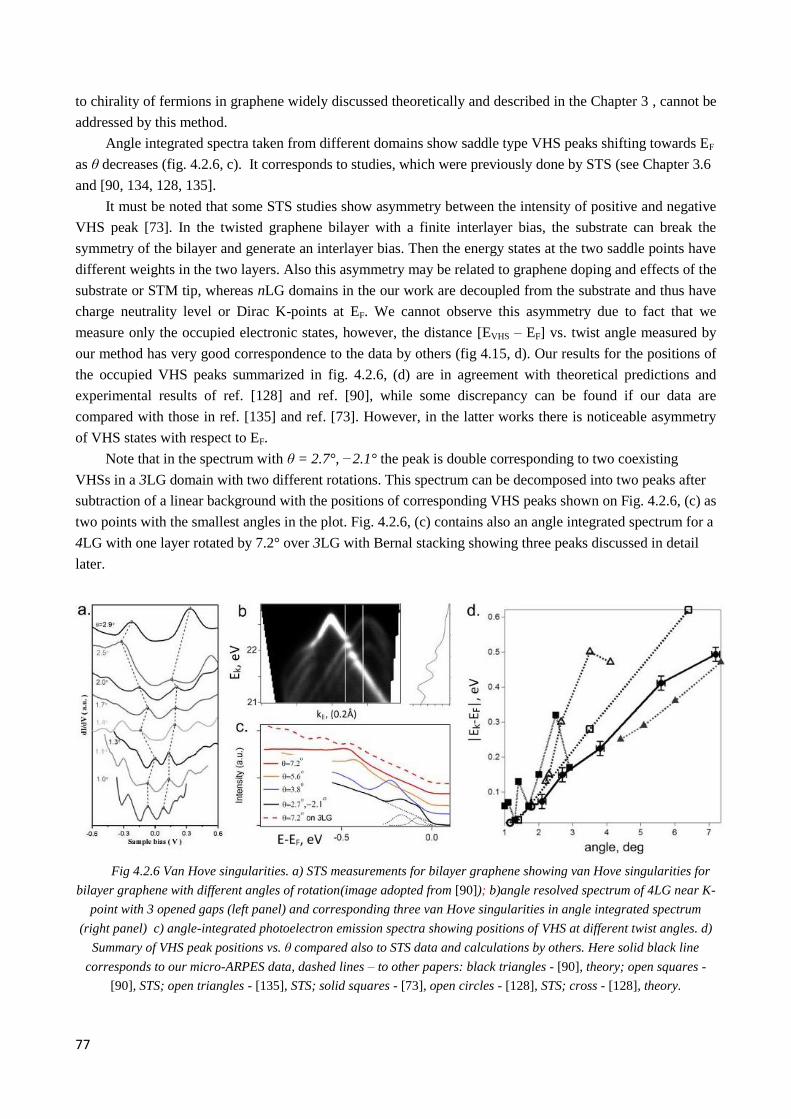
77
to chirality of fermions in graphene widely discussed theoretically and described in the Chapter 3 , cannot be
addressed by this method.
Angle integrated spectra taken from different domains show saddle type VHS peaks shifting towards EF
as θ decreases (fig. 4.2.6, c). It corresponds to studies, which were previously done by STS (see Chapter 3.6
and [90, 134, 128, 135].
It must be noted that some STS studies show asymmetry between the intensity of positive and negative
VHS peak [73]. In the twisted graphene bilayer with a finite interlayer bias, the substrate can break the
symmetry of the bilayer and generate an interlayer bias. Then the energy states at the two saddle points have
different weights in the two layers. Also this asymmetry may be related to graphene doping and effects of the
substrate or STM tip, whereas nLG domains in the our work are decoupled from the substrate and thus have
charge neutrality level or Dirac K-points at EF. We cannot observe this asymmetry due to fact that we
measure only the occupied electronic states, however, the distance [EVHS – EF] vs. twist angle measured by
our method has very good correspondence to the data by others (fig 4.15, d). Our results for the positions of
the occupied VHS peaks summarized in fig. 4.2.6, (d) are in agreement with theoretical predictions and
experimental results of ref. [128] and ref. [90], while some discrepancy can be found if our data are
compared with those in ref. [135] and ref. [73]. However, in the latter works there is noticeable asymmetry
of VHS states with respect to EF.
Note that in the spectrum with θ = 2.7°, −2.1° the peak is double corresponding to two coexisting
VHSs in a 3LG domain with two different rotations. This spectrum can be decomposed into two peaks after
subtraction of a linear background with the positions of corresponding VHS peaks shown on Fig. 4.2.6, (c) as
two points with the smallest angles in the plot. Fig. 4.2.6, (c) contains also an angle integrated spectrum for a
4LG with one layer rotated by 7.2° over 3LG with Bernal stacking showing three peaks discussed in detail
later.
Fig 4.2.6 Van Hove singularities. a) STS measurements for bilayer graphene showing van Hove singularities for
bilayer graphene with different angles of rotation(image adopted from [90]); b)angle resolved spectrum of 4LG near K-
point with 3 opened gaps (left panel) and corresponding three van Hove singularities in angle integrated spectrum
(right panel) c) angle-integrated photoelectron emission spectra showing positions of VHS at different twist angles. d)
Summary of VHS peak positions vs. θ compared also to STS data and calculations by others. Here solid black line
corresponds to our micro-ARPES data, dashed lines – to other papers: black triangles - [90], theory; open squares -
[90], STS; open triangles - [135], STS; solid squares - [73], open circles - [128], STS; cross - [128], theory.
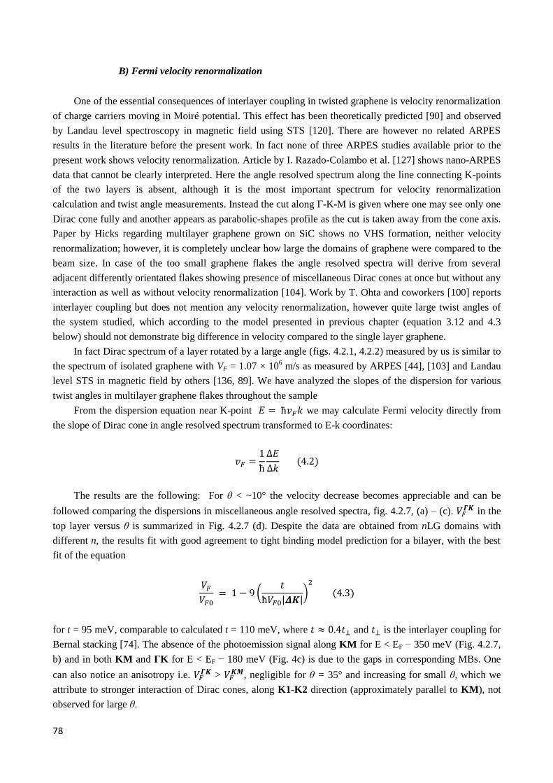
78
B) Fermi velocity renormalization
One of the essential consequences of interlayer coupling in twisted graphene is velocity renormalization
of charge carriers moving in Moiré potential. This effect has been theoretically predicted [90] and observed
by Landau level spectroscopy in magnetic field using STS [120]. There are however no related ARPES
results in the literature before the present work. In fact none of three ARPES studies available prior to the
present work shows velocity renormalization. Article by I. Razado-Colambo et al. [127] shows nano-ARPES
data that cannot be clearly interpreted. Here the angle resolved spectrum along the line connecting K-points
of the two layers is absent, although it is the most important spectrum for velocity renormalization
calculation and twist angle measurements. Instead the cut along Г-K-M is given where one may see only one
Dirac cone fully and another appears as parabolic-shapes profile as the cut is taken away from the cone axis.
Paper by Hicks regarding multilayer graphene grown on SiC shows no VHS formation, neither velocity
renormalization; however, it is completely unclear how large the domains of graphene were compared to the
beam size. In case of the too small graphene flakes the angle resolved spectra will derive from several
adjacent differently orientated flakes showing presence of miscellaneous Dirac cones at once but without any
interaction as well as without velocity renormalization [104]. Work by T. Ohta and coworkers [100] reports
interlayer coupling but does not mention any velocity renormalization, however quite large twist angles of
the system studied, which according to the model presented in previous chapter (equation 3.12 and 4.3
below) should not demonstrate big difference in velocity compared to the single layer graphene.
In fact Dirac spectrum of a layer rotated by a large angle (figs. 4.2.1, 4.2.2) measured by us is similar to
the spectrum of isolated graphene with VF = 1.07 × 10⁶ m/s as measured by ARPES [44], [103] and Landau
level STS in magnetic field by others [136, 89]. We have analyzed the slopes of the dispersion for various
twist angles in multilayer graphene flakes throughout the sample
From the dispersion equation near K-point 𝐸 = ħ𝑣𝐹𝑘 we may calculate Fermi velocity directly from
the slope of Dirac cone in angle resolved spectrum transformed to E-k coordinates:
𝑣𝐹 =1
ħ
∆𝐸
∆𝑘 (4.2)
The results are the following: For θ < ~10° the velocity decrease becomes appreciable and can be
followed comparing the dispersions in miscellaneous angle resolved spectra, fig. 4.2.7, (a) – (c). 𝑉𝐹𝜞𝑲 in the
top layer versus θ is summarized in Fig. 4.2.7 (d). Despite the data are obtained from nLG domains with
different n, the results fit with good agreement to tight binding model prediction for a bilayer, with the best
fit of the equation
𝑉𝐹
𝑉𝐹0 = 1 − 9 (
𝑡
ћ𝑉𝐹0|𝜟𝑲|)
2
(4.3)
for t = 95 meV, comparable to calculated t = 110 meV, where 𝑡 ≈ 0.4𝑡⊥ and 𝑡⊥ is the interlayer coupling for
Bernal stacking [74]. The absence of the photoemission signal along KM for E < EF − 350 meV (Fig. 4.2.7,
b) and in both KM and ΓK for E < EF − 180 meV (Fig. 4c) is due to the gaps in corresponding MBs. One
can also notice an anisotropy i.e. 𝑉𝐹𝜞𝑲 > 𝑉𝐹
𝑲𝑴, negligible for θ = 35° and increasing for small θ, which we
attribute to stronger interaction of Dirac cones, along K1-K2 direction (approximately parallel to KM), not
observed for large θ.
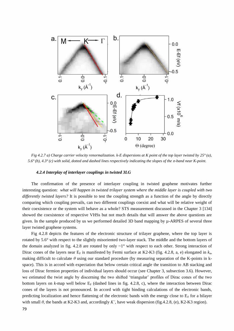
79
Fig 4.2.7 a) Charge carrier velocity renormalization. k-E dispersions at K point of the top layer twisted by 25° (a),
5.6° (b), 4.3° (c) with solid, dotted and dashed lines respectively indicating the slopes of the π-band near K-point.
4.2.4 Interplay of interlayer couplings in twisted 3LG
The confirmation of the presence of interlayer coupling in twisted graphene motivates further
interesting question: what will happen in twisted trilayer system where the middle layer is coupled with two
differently twisted layers? It is possible to test the coupling strength as a function of the angle by directly
comparing which coupling prevails, can two different couplings coexist and what will be relative weight of
their coexistence or the system will behave as a whole? STS measurement discussed in the Chapter 3 [134]
showed the coexistence of respective VHSs but not much details that will answer the above questions are
given. In the sample produced by us we performed detailed 3D band mapping by µ-ARPES of several three
layer twisted graphene systems.
Fig 4.2.8 depicts the features of the electronic structure of trilayer graphene, where the top layer is
rotated by 5.6° with respect to the slightly misoriented two-layer stack. The middle and the bottom layers of
the domain analyzed in fig. 4.2.8 are rotated by only ~1° with respect to each other. Strong interaction of
Dirac cones of the layers near EF is manifested by Fermi surface at K2-K3 (fig. 4.2.8, a, e) elongated in kx,
making difficult to calculate θ using our standard procedure (by measuring separation of the K-points in k-
space). This is in accord with expectation that below certain critical angle the transition to AB stacking and
loss of Dirac fermion properties of individual layers should occur (see Chapter 3, subsection 3.6). However,
we estimated the twist angle by discerning the two shifted ‘triangular’ profiles of Dirac cones of the two
bottom layers on k-map well below EF (dashed lines in fig. 4.2.8, c), where the interaction between Dirac
cones of the layers is not pronounced. In accord with tight binding calculations of the electronic bands,
predicting localization and hence flattening of the electronic bands with the energy close to EF for a bilayer
with small θ, the bands at K2-K3 and, accordingly K’, have weak dispersion (fig.4.2.8, (e), K2-K3 region).
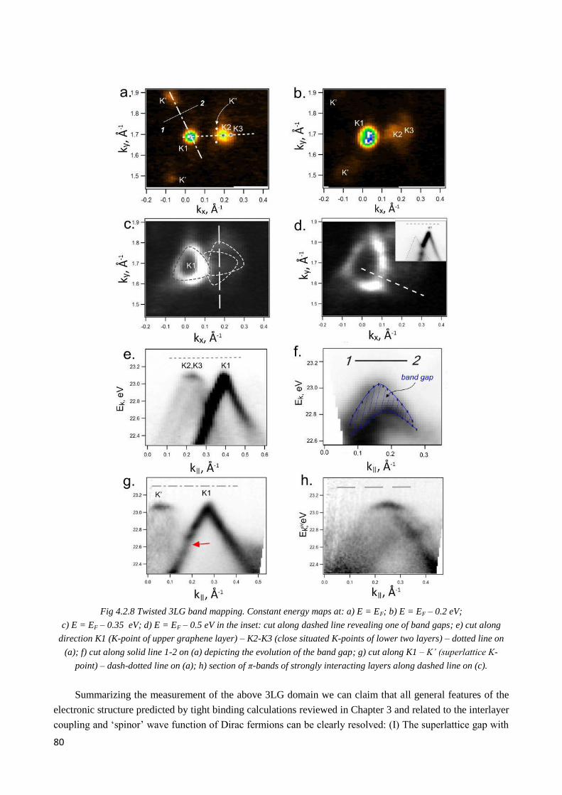
80
Fig 4.2.8 Twisted 3LG band mapping. Constant energy maps at: a) E = EF; b) E = EF – 0.2 eV;
c) E = EF – 0.35 eV; d) E = EF – 0.5 eV in the inset: cut along dashed line revealing one of band gaps; e) cut along
direction K1 (K-point of upper graphene layer) – K2-K3 (close situated K-points of lower two layers) – dotted line on
(a); f) cut along solid line 1-2 on (a) depicting the evolution of the band gap; g) cut along K1 – K’ (superlattice K-
point) – dash-dotted line on (a); h) section of π-bands of strongly interacting layers along dashed line on (c).
Summarizing the measurement of the above 3LG domain we can claim that all general features of the
electronic structure predicted by tight binding calculations reviewed in Chapter 3 and related to the interlayer
coupling and ‘spinor’ wave function of Dirac fermions can be clearly resolved: (I) The superlattice gap with
81
the maximum opening of ~175 meV (at corners of triangle in fig. 4.2.8, (d), showed in details in fig 4.2.8, (f)
and corresponding section shown on 4.2.8, (d, inset) is non-uniform along MB, which can be correlated with
calculations mentioned above in Chapter 3, (fig. 3.1.2, c). The bands manifest 2/3π rotational symmetry
around K as shown in fig. 4.2.8, (d) with zero gap along ΓK, while clearly open in KM (fig. 4.2.8, g,
indicated by arrow); (II) The minizone has additional superlattice zero gap points below EF. For θ = 5.6°
such points are found in the middle between K1 and K2, K1 and K’ etc., representing half of the
theoretically predicted points for ‘even’ type superlattice [81]. We speculate that only half of the expected
points are visible has the same origin because we see only half of the expected K' points, which is related to
umklapp processes and/or dark corridor of photoemission in graphene (see Chapter 3, paragraph 3.9 ) As
shown above (fig. 4.2.4) we observe also ‘odd’ type superlattices, e.g. for θ = 4.3°, where the points in the
middle between K1 and K2, K1 and K’ correspond to the maximum MB gap opening (fig. 4.2.8, f), making
characteristic difference between these two types of superlattices with the gap between K1 and K2 present
for the ‘odd’ (fig. 4.2.4, c) and absent for the ‘even’ (fig. 4.2.4, f) structures; vF of the charge carriers in the
top layer is renormalized from ~1.1 × 10⁶ m/s of isolated graphene to 0.71 × 10
6 m/s (fig. 4.2.7, b) in
quantitative agreement with tight binding model predictions [74] for a bilayer with θ = 5.6°
All the discussion above is also characteristic for the twisted bilayer graphene and is in accordance with
STS measurements about coexistence of VHSs in multilayers [129]. One of the most important observations
in these trilayer stack is the nonequivalence of the mutual impact, i.e. of the coupling strength, of the
differently rotated layers, which naturally results in different carrier velocities in the different layers. In the
first layer, which is rotated by bigger angle with respect to other two layers and consecutively feels less
interaction, Fermi velocity is renormalized but still equal to 70% of that one of free-standing graphene. That
is much higher that the velocity in the lower bilayer with small angle of misorientation between layers.
Fig 4.2.9 depicts the similar to previously discussed system, however, here the middle layer is rotated
by 2.7º with respect to the topmost and by 2.1º by with respect to the third layer, so the rotation between top
and bottom layers is just ~0.6 º. Due to such small angle of separation between corresponding K-points it is
hard to discern clearly Dirac cone of the lowest layer, so on the fig 4.2.9, (b) we may see only faint signature
of the which is shaded by much more intensive band of the topmost one. However we clearly observe the
superlattice points for both subsystems, which are well separated from the main K-points (fig 4.2.9, a): here
the points K’ originate from the L1-L2 superstructure and K” originate from L2-L3 (fig 4.2.9, a) and thus we
may conclude that this structure is a trilayer. We may directly observe the significant difference in the slope
angle for topmost layer’s π-band and the replica bands equivalent to middle and bottom layers at the cut
through points K1, K’ and K” presented on the fig 4.2.9, (b and c). Here we again observe similar to the
previously discussed 3LG nonequivalence in group velocities of the charge carriers in different layers.
Topmost layer, being rotated by bigger angle has vF = 0.35·106 m/s, while lower two layers, have vF =
0.2·106 m/s. These can be observed on angle resolved spectra on fig. 4.2.9, (b), (c) as the slopes of the π-band
are seen steeper for topmost (K1) than for K2-K3 layers (b) and corresponding replica bands (c). Thus, for
this system the difference of rotation only in 0.6º (2.7º vs 2.1º) changes the strength of the coupling
dramatically: the top layer rotated by slightly bigger angle with respect to the middle interacts less than the
bottom one and corresponding charge carriers group velocities differ almost by factor of 2.
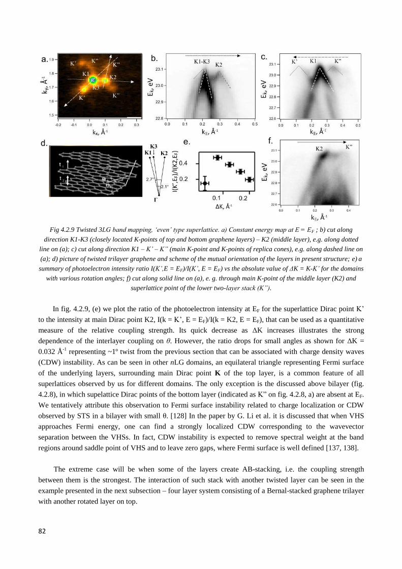
82
Fig 4.2.9 Twisted 3LG band mapping, ‘even’ type superlattice. a) Constant energy map at E = EF ; b) cut along
direction K1-K3 (closely located K-points of top and bottom graphene layers) – K2 (middle layer), e.g. along dotted
line on (a); c) cut along direction K1 – K’ – K” (main K-point and K-points of replica cones), e.g. along dashed line on
(a); d) picture of twisted trilayer graphene and scheme of the mutual orientation of the layers in present structure; e) a
summary of photoelectron intensity ratio I(K’,E = EF)/I(K’, E = EF) vs the absolute value of ΔK = K-K’ for the domains
with various rotation angles; f) cut along solid line on (a), e. g. through main K-point of the middle layer (K2) and
superlattice point of the lower two-layer stack (K”).
In fig. 4.2.9, (e) we plot the ratio of the photoelectron intensity at EF for the superlattice Dirac point K’
to the intensity at main Dirac point K2, I(k = K’, E = EF)/I(k = K2, E = EF), that can be used as a quantitative
measure of the relative coupling strength. Its quick decrease as ΔK increases illustrates the strong
dependence of the interlayer coupling on θ. However, the ratio drops for small angles as shown for ΔK =
0.032 Å-1
representing ~1º twist from the previous section that can be associated with charge density waves
(CDW) instability. As can be seen in other nLG domains, an equilateral triangle representing Fermi surface
of the underlying layers, surrounding main Dirac point K of the top layer, is a common feature of all
superlattices observed by us for different domains. The only exception is the discussed above bilayer (fig.
4.2.8), in which supelattice Dirac points of the bottom layer (indicated as K” on fig. 4.2.8, a) are absent at EF.
We tentatively attribute this observation to Fermi surface instability related to charge localization or CDW
observed by STS in a bilayer with small θ. [128] In the paper by G. Li et al. it is discussed that when VHS
approaches Fermi energy, one can find a strongly localized CDW corresponding to the wavevector
separation between the VHSs. In fact, CDW instability is expected to remove spectral weight at the band
regions around saddle point of VHS and to leave zero gaps, where Fermi surface is well defined [137, 138].
The extreme case will be when some of the layers create AB-stacking, i.e. the coupling strength
between them is the strongest. The interaction of such stack with another twisted layer can be seen in the
example presented in the next subsection – four layer system consisting of a Bernal-stacked graphene trilayer
with another rotated layer on top.
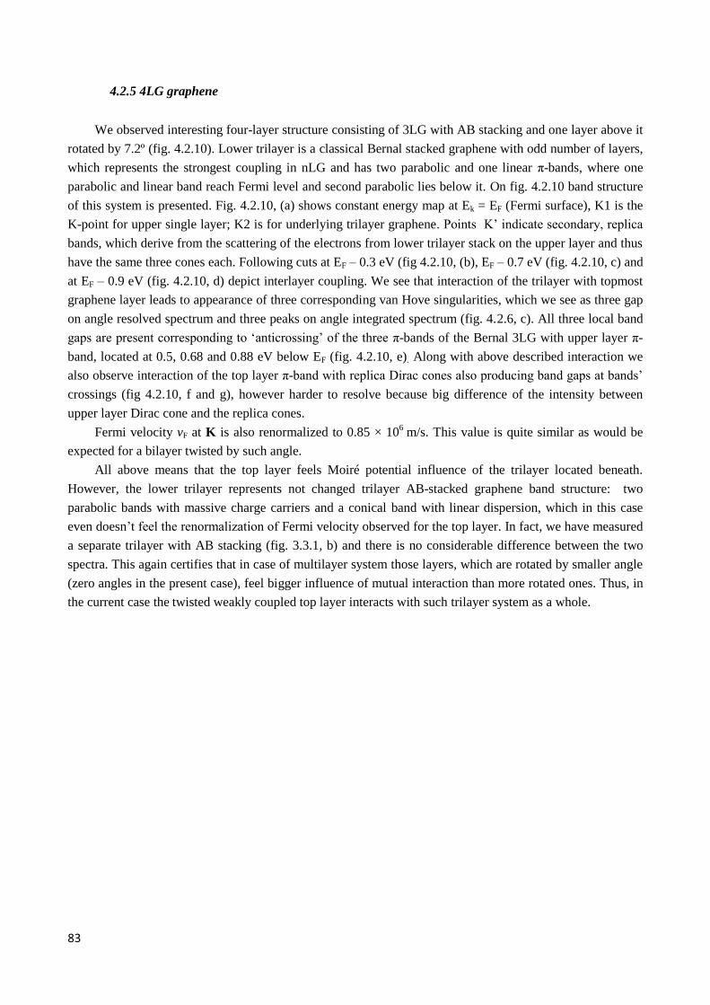
83
4.2.5 4LG graphene
We observed interesting four-layer structure consisting of 3LG with AB stacking and one layer above it
rotated by 7.2º (fig. 4.2.10). Lower trilayer is a classical Bernal stacked graphene with odd number of layers,
which represents the strongest coupling in nLG and has two parabolic and one linear π-bands, where one
parabolic and linear band reach Fermi level and second parabolic lies below it. On fig. 4.2.10 band structure
of this system is presented. Fig. 4.2.10, (a) shows constant energy map at Ek = EF (Fermi surface), K1 is the
K-point for upper single layer; K2 is for underlying trilayer graphene. Points K’ indicate secondary, replica
bands, which derive from the scattering of the electrons from lower trilayer stack on the upper layer and thus
have the same three cones each. Following cuts at EF – 0.3 eV (fig 4.2.10, (b), EF – 0.7 eV (fig. 4.2.10, c) and
at EF – 0.9 eV (fig. 4.2.10, d) depict interlayer coupling. We see that interaction of the trilayer with topmost
graphene layer leads to appearance of three corresponding van Hove singularities, which we see as three gap
on angle resolved spectrum and three peaks on angle integrated spectrum (fig. 4.2.6, c). All three local band
gaps are present corresponding to ‘anticrossing’ of the three π-bands of the Bernal 3LG with upper layer π-
band, located at 0.5, 0.68 and 0.88 eV below EF (fig. 4.2.10, e). Along with above described interaction we
also observe interaction of the top layer π-band with replica Dirac cones also producing band gaps at bands’
crossings (fig 4.2.10, f and g), however harder to resolve because big difference of the intensity between
upper layer Dirac cone and the replica cones.
Fermi velocity vF at K is also renormalized to 0.85 × 10⁶ m/s. This value is quite similar as would be
expected for a bilayer twisted by such angle.
All above means that the top layer feels Moiré potential influence of the trilayer located beneath.
However, the lower trilayer represents not changed trilayer AB-stacked graphene band structure: two
parabolic bands with massive charge carriers and a conical band with linear dispersion, which in this case
even doesn’t feel the renormalization of Fermi velocity observed for the top layer. In fact, we have measured
a separate trilayer with AB stacking (fig. 3.3.1, b) and there is no considerable difference between the two
spectra. This again certifies that in case of multilayer system those layers, which are rotated by smaller angle
(zero angles in the present case), feel bigger influence of mutual interaction than more rotated ones. Thus, in
the current case the twisted weakly coupled top layer interacts with such trilayer system as a whole.
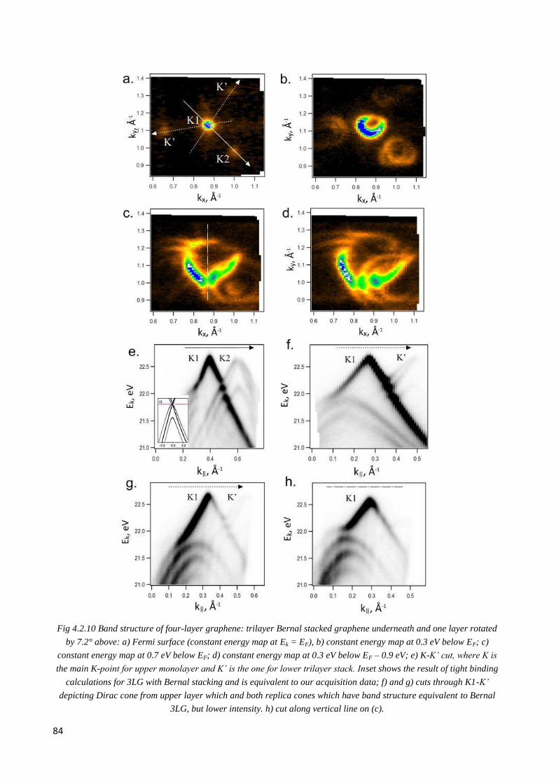
84
Fig 4.2.10 Band structure of four-layer graphene: trilayer Bernal stacked graphene underneath and one layer rotated
by 7.2° above: a) Fermi surface (constant energy map at Ek = EF), b) constant energy map at 0.3 eV below EF; c)
constant energy map at 0.7 eV below EF; d) constant energy map at 0.3 eV below EF – 0.9 eV; e) K-K’ cut, where K is
the main K-point for upper monolayer and K’ is the one for lower trilayer stack. Inset shows the result of tight binding
calculations for 3LG with Bernal stacking and is equivalent to our acquisition data; f) and g) cuts through K1-K’
depicting Dirac cone from upper layer which and both replica cones which have band structure equivalent to Bernal
3LG, but lower intensity. h) cut along vertical line on (c).
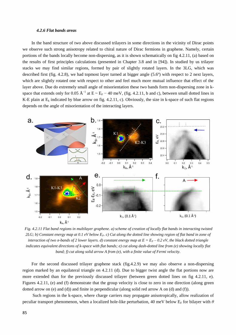
85
4.2.6 Flat bands areas
In the band structure of two above discussed trilayers in some directions in the vicinity of Dirac points
we observe such strong anisotropy related to chiral nature of Dirac fermions in graphene. Namely, certain
portions of the bands locally become non-dispersing, as it is shown schematically on fig 4.2.11, (a) based on
the results of first principles calculations (presented in Chapter 3.8 and in [94]). In studied by us trilayer
stacks we may find similar regions, formed by pair of slightly rotated layers. In the 3LG, which was
described first (fig. 4.2.8), we had topmost layer turned at bigger angle (5.6º) with respect to 2 next layers,
which are slightly rotated one with respect to other and feel much more mutual influence that effect of the
layer above. Due do extremely small angle of misorientation these two bands form non-dispersing zone in k-
space that extends only for 0.05 Å−1
at E ~ EF − 40 meV, (fig. 4.2.11, b and c), between small dotted lines in
K-E plain at Ek indicated by blue arrow on fig. 4.2.11, c). Obviously, the size in k-space of such flat regions
depends on the angle of misorientation of the interacting layers.
Fig. 4.2.11 Flat band regions in multilayer graphene. a) scheme of creation of locally flat bands in interacting twisted
2LG; b) Constant energy map at 0.1 eV below EF. c) Cut along the dotted line showing region of flat band in zone of
interaction of two π-bands of 2 lower layers. d) constant energy map at E = EF – 0.2 eV, the black dotted triangle
indicates equivalent directions of k-space with flat bands; e) cut along dash-dotted line from (e) showing locally flat
band; f) cut along solid arrow A from (e), with a finite value of Fermi velocity.
For the second discussed trilayer graphene stack (fig.4.2.9) we may also observe a non-dispersing
region marked by an equilateral triangle on 4.2.11 (d). Due to bigger twist angle the flat portions now are
more extended than for the previously discussed trilayer (between green dotted lines on fig 4.2.11, e).
Figures 4.2.11, (e) and (f) demonstrate that the group velocity is close to zero in one direction (along green
dotted arrow on (e) and (d)) and finite in perpendicular (along solid red arrow A on (d) and (f)).
Such regions in the k-space, where charge carriers may propagate anisotropically, allow realization of
peculiar transport phenomenon, when a localized hole-like perturbation, 40 meV below EF for bilayer with θ

86
~ 1° (fig. 4.2.11, c), and 65 meV for the one with θ ~2.1º (fig. 4.2.11, e), would propagate with a group
velocity V = ћ−1∇kE perpendicular to the flat band in the direction indicated by the arrow A and also along its
symmetrically equivalent directions. Linear (or ‘quasi-one-dimensional’) propagation of the wave package in
a system with flat band portion was shown to be much more effective than in two-dimentional potential. It
was simulated by L. Xian et al. [94] that was mentioned above in Chapter 3.4.4 (fig. 3.4.7).
For second 3LG domain discussed in fig. 4.2.9 the group velocity can be estimated as ~1.5 × 10⁻⁵
m/s
from the corresponding k-E dispersion in fig. 4.2.11, (f) whereas for the first domain it is hard to estimate the
velocity due to small extension of the flat portion of the band in k-space. We could find clear evidence of the
flat bands, which may be used to realize one-dimensional transport, in the minizones corresponding only to
small θ such as 1-2.1º presented in the last subsections. In both cases shift of EF needed for switching to
quasi-one-dimensional conductivity is less than 100 meV and can be achieved by small doping level below
0.003 e- per unit cell, not changing bilayer electronic structure if each layer is doped by the same amount or
eventually by external field effect gating.
4.2.7 Summary of the current chapter and motivation for the further experiments
First of all we bridged the theoretical predictions for interlayer coupling in twisted bilayers that were
only partially verified by STM-STS. We showed:
1) velocity renormalization in twisted graphene carriers due to Moiré potential;
2) non-uniform band gap along twisted graphene K- minizone boundary;
3) different band structures of different type superlattices;
4) relation of interlayer strength vs. twist angle for various trilayer systems.
Summarizing the latter (4) results we can conclude that on the different ‘floors’ of twisted nLG domain
the charge carriers can propagate with different group velocities and, if a given layer is found between the
two layers with different twist angles, smaller rotation has bigger influence on the electronic structure of the
layer.
As presented above, the rich variety of electronic structure phenomena giving a possibility of a wide
range tuning of the electronic structure of twisted few layer graphene is observed. In the presence of several
interlayer couplings the electronic properties can be completely different in different layers of the same
domain providing independent channels of electron transport. The group velocity of the charge carriers
propagating in the moiré potential of strongly coupled (slightly twisted with θ < 2.5°) layers is not only
renormalized, but can be anisotropic, giving unique possibility to transform the graphene from the two-
dimensional into a quasi-one-dimensional conductor using two tuning parameters: θ and EF shift by doping.
The later finding originally motivated our research described in the following chapter. The flat bands
observed are below the EF by few tens of meV. If we manage to bring the EF at the potition of VHS then
quasi one dimensional transport can be potentially realized in graphene. There are, however, some
fundamental questions, regarding realization of such system arising. If the shift of Fermi level is attempted
by perpendicular filed effect, the field across the bilayer structure can be screened from the first layer to the
second and the doping between the layers will be non-uniform. If Fermi level is moved by means of
intercalation of, e.g. alkali metals, the effect can be similar and also the atoms penetrating between graphene
layers can modify eventually the graphene interlayer coupling. The existence of van Hove singularities
should also be verified upon alkali metal doping. In the following chapter we demonstrate that the
singularities, and hence interlayer coupling, remain and we demonstrate unexpected splitting in the middle
layer bands of trilayer system doped by alkali metals atoms.
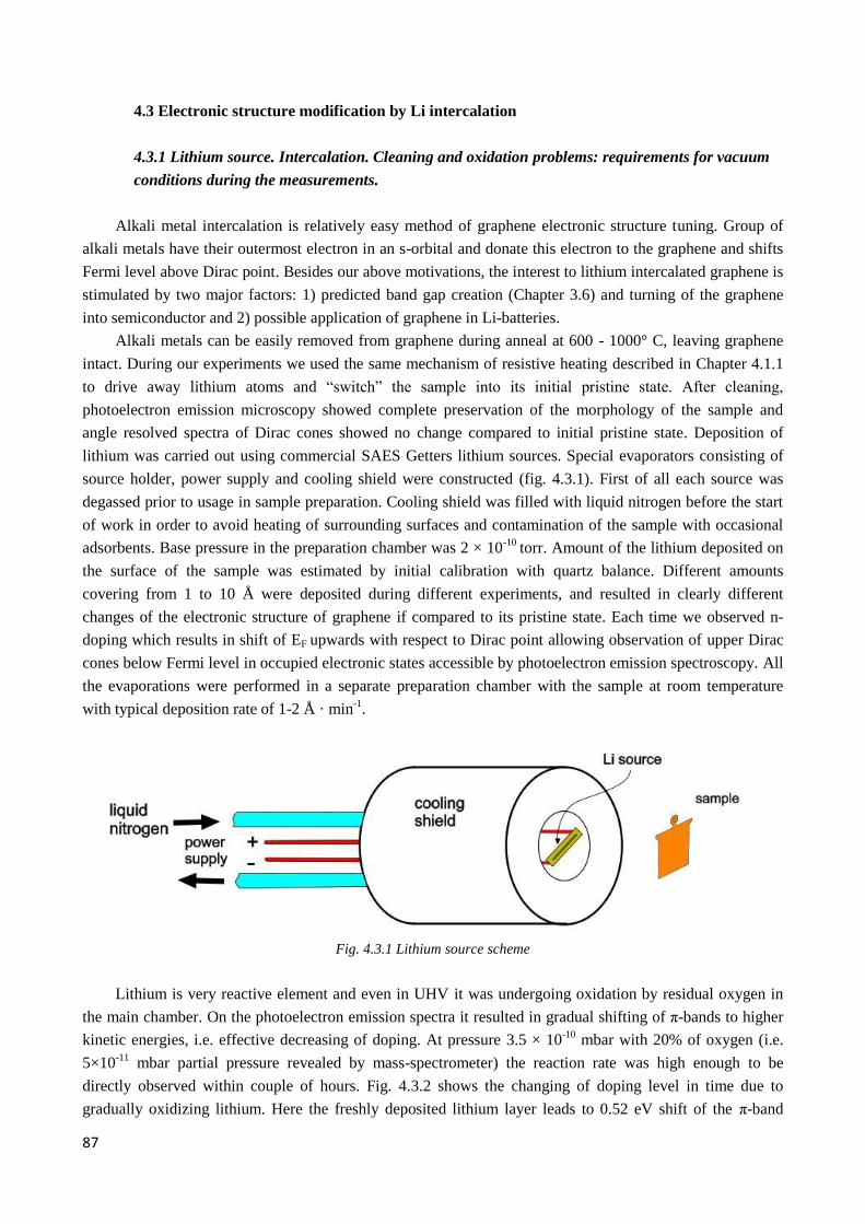
87
4.3 Electronic structure modification by Li intercalation
4.3.1 Lithium source. Intercalation. Cleaning and oxidation problems: requirements for vacuum
conditions during the measurements.
Alkali metal intercalation is relatively easy method of graphene electronic structure tuning. Group of
alkali metals have their outermost electron in an s-orbital and donate this electron to the graphene and shifts
Fermi level above Dirac point. Besides our above motivations, the interest to lithium intercalated graphene is
stimulated by two major factors: 1) predicted band gap creation (Chapter 3.6) and turning of the graphene
into semiconductor and 2) possible application of graphene in Li-batteries.
Alkali metals can be easily removed from graphene during anneal at 600 - 1000° C, leaving graphene
intact. During our experiments we used the same mechanism of resistive heating described in Chapter 4.1.1
to drive away lithium atoms and “switch” the sample into its initial pristine state. After cleaning,
photoelectron emission microscopy showed complete preservation of the morphology of the sample and
angle resolved spectra of Dirac cones showed no change compared to initial pristine state. Deposition of
lithium was carried out using commercial SAES Getters lithium sources. Special evaporators consisting of
source holder, power supply and cooling shield were constructed (fig. 4.3.1). First of all each source was
degassed prior to usage in sample preparation. Cooling shield was filled with liquid nitrogen before the start
of work in order to avoid heating of surrounding surfaces and contamination of the sample with occasional
adsorbents. Base pressure in the preparation chamber was 2 × 10⁻¹⁰
torr. Amount of the lithium deposited on
the surface of the sample was estimated by initial calibration with quartz balance. Different amounts
covering from 1 to 10 Å were deposited during different experiments, and resulted in clearly different
changes of the electronic structure of graphene if compared to its pristine state. Each time we observed n-
doping which results in shift of EF upwards with respect to Dirac point allowing observation of upper Dirac
cones below Fermi level in occupied electronic states accessible by photoelectron emission spectroscopy. All
the evaporations were performed in a separate preparation chamber with the sample at room temperature
with typical deposition rate of 1-2 Å · min-1
.
Fig. 4.3.1 Lithium source scheme
Lithium is very reactive element and even in UHV it was undergoing oxidation by residual oxygen in
the main chamber. On the photoelectron emission spectra it resulted in gradual shifting of π-bands to higher
kinetic energies, i.e. effective decreasing of doping. At pressure 3.5 × 10⁻¹⁰
mbar with 20% of oxygen (i.e.
5×10-11
mbar partial pressure revealed by mass-spectrometer) the reaction rate was high enough to be
directly observed within couple of hours. Fig. 4.3.2 shows the changing of doping level in time due to
gradually oxidizing lithium. Here the freshly deposited lithium layer leads to 0.52 eV shift of the π-band
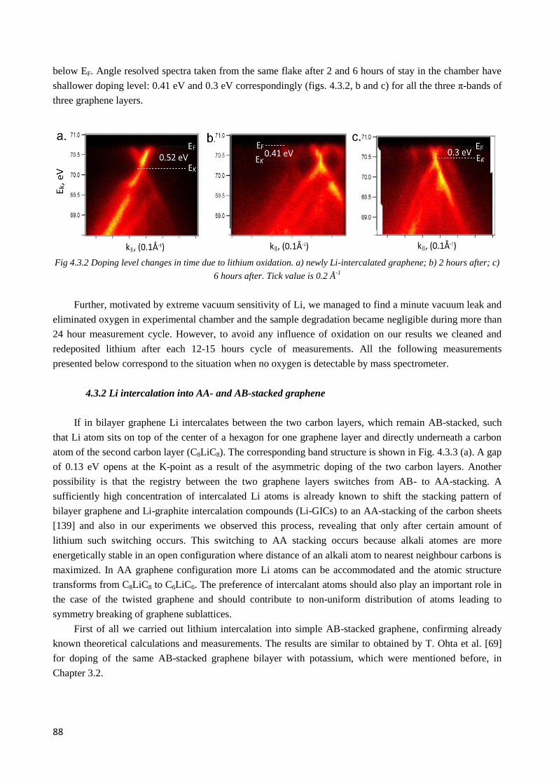
88
below EF. Angle resolved spectra taken from the same flake after 2 and 6 hours of stay in the chamber have
shallower doping level: 0.41 eV and 0.3 eV correspondingly (figs. 4.3.2, b and c) for all the three π-bands of
three graphene layers.
Fig 4.3.2 Doping level changes in time due to lithium oxidation. a) newly Li-intercalated graphene; b) 2 hours after; c)
6 hours after. Tick value is 0.2 Å-1
Further, motivated by extreme vacuum sensitivity of Li, we managed to find a minute vacuum leak and
eliminated oxygen in experimental chamber and the sample degradation became negligible during more than
24 hour measurement cycle. However, to avoid any influence of oxidation on our results we cleaned and
redeposited lithium after each 12-15 hours cycle of measurements. All the following measurements
presented below correspond to the situation when no oxygen is detectable by mass spectrometer.
4.3.2 Li intercalation into AA- and AB-stacked graphene
If in bilayer graphene Li intercalates between the two carbon layers, which remain AB-stacked, such
that Li atom sits on top of the center of a hexagon for one graphene layer and directly underneath a carbon
atom of the second carbon layer (C8LiC8). The corresponding band structure is shown in Fig. 4.3.3 (a). A gap
of 0.13 eV opens at the K-point as a result of the asymmetric doping of the two carbon layers. Another
possibility is that the registry between the two graphene layers switches from AB- to AA-stacking. A
sufficiently high concentration of intercalated Li atoms is already known to shift the stacking pattern of
bilayer graphene and Li-graphite intercalation compounds (Li-GICs) to an AA-stacking of the carbon sheets
[139] and also in our experiments we observed this process, revealing that only after certain amount of
lithium such switching occurs. This switching to AA stacking occurs because alkali atomes are more
energetically stable in an open configuration where distance of an alkali atom to nearest neighbour carbons is
maximized. In AA graphene configuration more Li atoms can be accommodated and the atomic structure
transforms from C8LiC8 to C6LiC6. The preference of intercalant atoms should also play an important role in
the case of the twisted graphene and should contribute to non-uniform distribution of atoms leading to
symmetry breaking of graphene sublattices.
First of all we carried out lithium intercalation into simple AB-stacked graphene, confirming already
known theoretical calculations and measurements. The results are similar to obtained by T. Ohta et al. [69]
for doping of the same AB-stacked graphene bilayer with potassium, which were mentioned before, in
Chapter 3.2.

89
Fig 4.3.3 π-band of AB staked bilayer graphene. a) Li-doped, theoretical calculations (image adopted from
[139]); b) micro-ARPES data, pristine graphene; c) micro-ARPES data for Li-doped graphene, same flake that in (b).
It is worth mentioning that in alkali intercalated (Bernal stacked) graphite a widening of interlayer
distance proportional to the size of the intercalated atom is observed. At low intercalant concentrations there
is a local widening (bump) of the interlayer distance where an intercalant is placed, while the rest of the van
der Waals heterostructure retains the interlayer spacing of the pristine bilayer system [140]. Intercalation
positions with a maximum cavity size are thus preferential in energy.
Here we report results on the four-layer graphene, consisted of two pairs of AB-stacked 2LG rotated by
30º, which band structure before Li intercalation was already described above, in section 4.2.1 (fig. 4.2.1, b-
d). On the constant energy map on fig 4.3.4, (b) we see Dirac points corresponding to both BLGs: brighter is
for upper and dimmer is for lower one. Constant energy map taken at 1.3 eV below Fermi lever shows
sections of π-band for all 4 layers (two pairs of coaxial cones, fig. 4.3.4, (c) and cut through K-points shows
the parabolic character of π-bands in the vicinity of Dirac point that confirms AB stacking for both bilayers
(fig. 4.3.4, (b), inset).
After intercalation of a moderate dose of lithium (~8 Å) we observed typical angle resolved spectrum
for doped AB bilayer with two π-bands of equal intensity, locally flat band sections in the vicinity of Dirac
point, and small band gap (about 0.15 eV) that can be seen on fig. 4.3.4, (d) similar to the reposrted in
calculations (fig. 4.3.3., a).
With the next step we increased the lithium dose significantly (to about 18Å) and found out that this
system does not look like Bernal-stacked graphene anymore: on the fig 4.3.4, (e) taken at K-point we
observe the above mentioned switch into AA-type stacking. One can see three π-bands which correspond to
positioning of the carbon atoms one atop of another (AAA-stack), thus creating more space for intercalated
between the sheets lithium atoms. Constant energy map at EF shows three ‘circles’ corresponding to three π-
bands. The shift of Dirac point from EF was ~0.65 eV after the first doping and ~1.05 eV after the second
one indicating bigger charge transfer from lithium to AA-stacked system.
For case of twisted graphene the situation is different, the doping shifts π-bands, but generally does not
alternate the layer interaction except some specific feature that will be shown later. In the following we did
not observe any reconstruction, such as a change in the twist angle upon twisted graphene doping. This is
expected, since translation with an atomic distance (AB -> AA) requires essentially smaller energy than
rotation of micrometric sized graphene layer even by a minute angle.
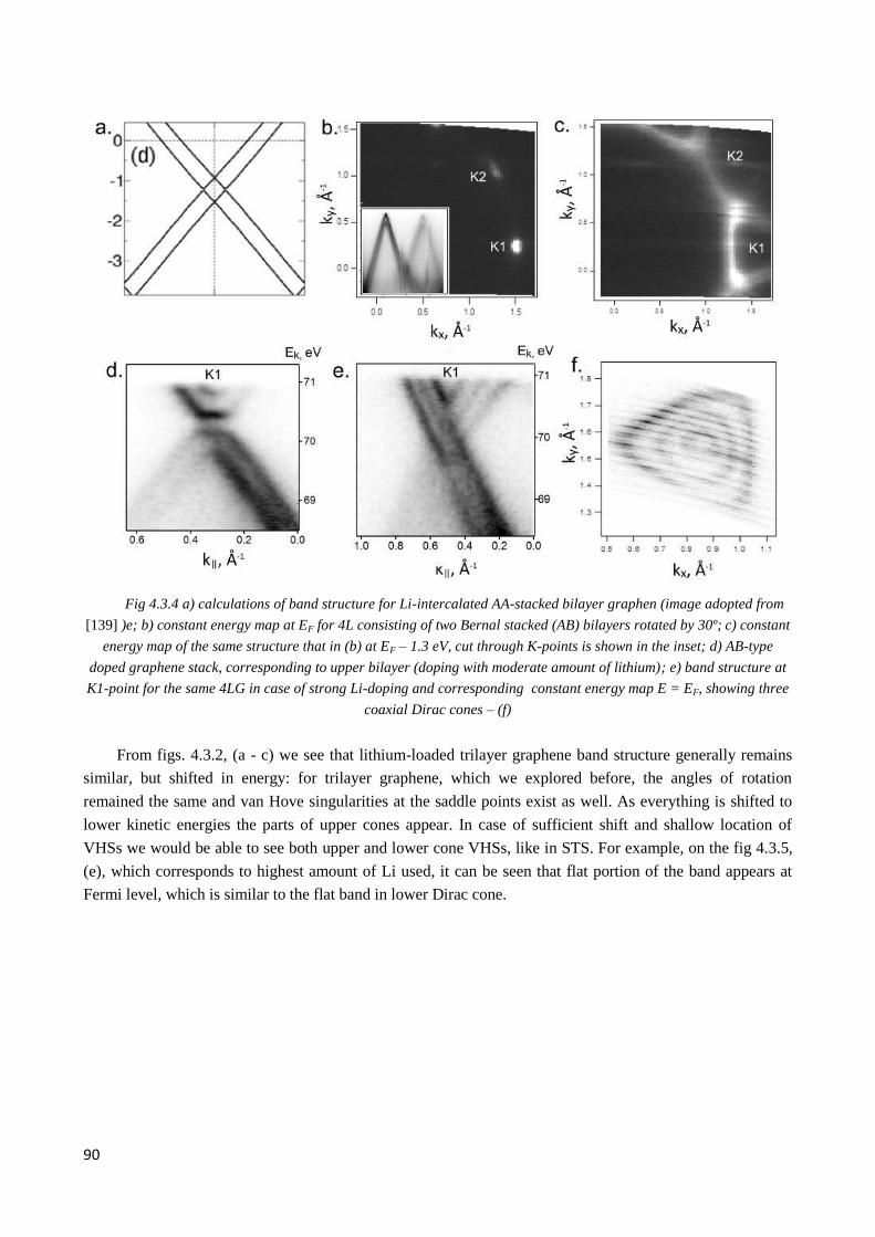
90
Fig 4.3.4 a) calculations of band structure for Li-intercalated AA-stacked bilayer graphen (image adopted from
[139] )e; b) constant energy map at EF for 4L consisting of two Bernal stacked (AB) bilayers rotated by 30º; c) constant
energy map of the same structure that in (b) at EF – 1.3 eV, cut through K-points is shown in the inset; d) AB-type
doped graphene stack, corresponding to upper bilayer (doping with moderate amount of lithium); e) band structure at
K1-point for the same 4LG in case of strong Li-doping and corresponding constant energy map E = EF, showing three
coaxial Dirac cones – (f)
From figs. 4.3.2, (a - c) we see that lithium-loaded trilayer graphene band structure generally remains
similar, but shifted in energy: for trilayer graphene, which we explored before, the angles of rotation
remained the same and van Hove singularities at the saddle points exist as well. As everything is shifted to
lower kinetic energies the parts of upper cones appear. In case of sufficient shift and shallow location of
VHSs we would be able to see both upper and lower cone VHSs, like in STS. For example, on the fig 4.3.5,
(e), which corresponds to highest amount of Li used, it can be seen that flat portion of the band appears at
Fermi level, which is similar to the flat band in lower Dirac cone.
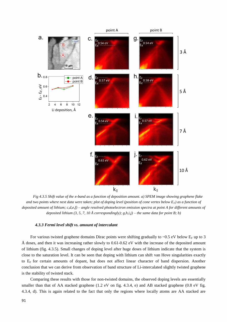
91
Fig 4.3.5 Shift value of the π-band as a function of deposition amount. a) SPEM image showing graphene flake
and two points where next data were taken; plot of doping level (position of cone vertex below EF) as a function of
deposited amount of lithium; c,d,e,f) – angle resolved photoelectron emission spectra at point A for different amounts of
deposited lithium (3, 5, 7, 10 Å correspondingly); g,h,i,j) – the same data for point B; b)
4.3.3 Fermi level shift vs. amount of intercalant
For various twisted graphene domains Dirac points were shifting gradually to ~0.5 eV below EF up to 3
Å doses, and then it was increasing rather slowly to 0.61-0.62 eV with the increase of the deposited amount
of lithium (fig. 4.3.5). Small changes of doping level after huge doses of lithium indicate that the system is
close to the saturation level. It can be seen that doping with lithium can shift van Hove singularities exactly
to EF for certain amounts of dopant, but does not affect linear character of band dispersion. Another
conclusion that we can derive from observation of band structure of Li-intercalated slightly twisted graphene
is the stability of twisted stack.
Comparing these results with those for non-twisted domains, the observed doping levels are essentially
smaller than that of AA stacked graphene (1.2 eV on fig. 4.3.4, e) and AB stacked graphene (0.8 eV fig.
4.3.4, d). This is again related to the fact that only the regions where locally atoms are AA stacked are

92
preferred for intercalating atoms, i.e. we can expect that maximum doping level of twisted graphene can
depend on the twist angle. We did not study such dependence systematically and in the following we present
two three layer twisted graphene stacks where the doping level of all three layers, despite the two different
twist angles, are very similar.
4.3.4 Initial band structure of two twisted 3LG domains selected for alkali metal atoms
intercalation
Discussed in the subsections 4.2.5 – 4.2.6 trilayer graphene structures are interesting in terms of
observation of graphene π-band behavior at extremely small angle of misalignment; however it is not an easy
task to discern separate bands in such systems. In case of doping by intercalation of alkali metals, which was
planned for next stage of studies it could be really complicated to unravel each band behavior, also because
of inhomogenieties inevitable during intercalation process leading to slight bands broadening observed by us.
To make the situation clearer we have chosen trilayer graphene flakes with bigger angles of rotation between
layers, which were further used for detailed measurements of the effects of alkali metal intercalation. Here
we discuss the structure of adjacent flakes that are both trilayer and have two almost equally oriented top and
bottom layers while the middle one with different angle for these two domains. Although we cannot confirm
because of limited lateral resolution but most probably the domains are formed by same top and bottom
sheets of graphene, while having different middle layer as depicted schematically on fig. 4.3.6, (a). The angle
are: A) rotation 6° between topmost and 2nd
layer and 7,3° between topmost and 3rd
layer; B) 3.6° and 7°
correspondingly; scheme for these structure is presented on fig. 4.3.6, (a). These stacks allow us to see
clearly all the three π-bands belonging to three graphene layers and also their interaction. Fig. 4.3.6, (b)
depicts SPEM image of the flakes, where the two studied trilayer graphene stacks were found; point A
corresponds to stack with rotation angles 6° and 7º between topmost/middle and topmost/bottom layers
correspondingly. In order to evidence the domains the analyzer position can be adjusted. First domain can be
seen as bright area on fig. 4.3.6 (lower panel, point A) and the second similarly was seen as bright are at
different position of the energy analyzer (fig. 4.3.6, upper panel, point B). In order to enhance the signal
from this particular flake the analyzer was turned towards K-point of middle layer (K2) and the area of
detector was limited in the way to leave aside the signal from adjacent K-points (K1 and K3). In this way the
maximum contribution was obtained from specifically rotated middle layer, which is rotated differently from
every other carbon layer around and thus can be seen as the brightest area in the SPEM image. For each
mentioned domain a full data set I(Ek, kx, ky) was acquired allowing examination of the band structure
features by taking plane cuts in all the directions around K1-K3 points. Such cuts through main K-points are
shown next to the corresponding flakes on fig. 4.3.6, (b).
Constant energy maps at E = EF clearly show main K-points which can be placed on the circle with
radius 1.75 Å-1
, corresponding to ΓK wave vector, belonging to three layers and have different intensity. The
brightest one (K1) is in the center and belong to the upper layer, second brightest (K2, upper left on the fig.
4.3.7, (a) belong to the middle layer and the third, K3 is of the third layer from the top and thus has the least
intensity of these three K-points. Except main K-points we also observe secondary ones which are attributed
to superlattice i.e. they are the K-points of Brillouin minizone formed by BZ of each single layer these points
are indicated as K’ on following figures. These superlattice Dirac cones which emerge due scattering are also
called ‘replica cones’ or ‘moiré bands’ as was discussed in the previous chapter 4.2.
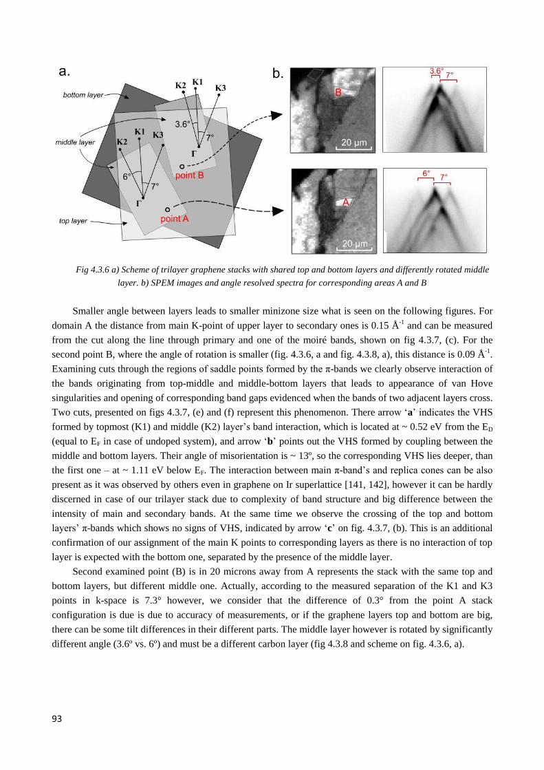
93
Fig 4.3.6 a) Scheme of trilayer graphene stacks with shared top and bottom layers and differently rotated middle
layer. b) SPEM images and angle resolved spectra for corresponding areas A and B
Smaller angle between layers leads to smaller minizone size what is seen on the following figures. For
domain A the distance from main K-point of upper layer to secondary ones is 0.15 Å-1
and can be measured
from the cut along the line through primary and one of the moiré bands, shown on fig 4.3.7, (c). For the
second point B, where the angle of rotation is smaller (fig. 4.3.6, a and fig. 4.3.8, a), this distance is 0.09 Å-1
.
Examining cuts through the regions of saddle points formed by the π-bands we clearly observe interaction of
the bands originating from top-middle and middle-bottom layers that leads to appearance of van Hove
singularities and opening of corresponding band gaps evidenced when the bands of two adjacent layers cross.
Two cuts, presented on figs 4.3.7, (e) and (f) represent this phenomenon. There arrow ‘a’ indicates the VHS
formed by topmost (K1) and middle (K2) layer’s band interaction, which is located at ~ 0.52 eV from the ED
(equal to EF in case of undoped system), and arrow ‘b’ points out the VHS formed by coupling between the
middle and bottom layers. Their angle of misorientation is ~ 13º, so the corresponding VHS lies deeper, than
the first one – at ~ 1.11 eV below EF. The interaction between main π-band’s and replica cones can be also
present as it was observed by others even in graphene on Ir superlattice [141, 142], however it can be hardly
discerned in case of our trilayer stack due to complexity of band structure and big difference between the
intensity of main and secondary bands. At the same time we observe the crossing of the top and bottom
layers’ π-bands which shows no signs of VHS, indicated by arrow ‘c’ on fig. 4.3.7, (b). This is an additional
confirmation of our assignment of the main K points to corresponding layers as there is no interaction of top
layer is expected with the bottom one, separated by the presence of the middle layer.
Second examined point (B) is in 20 microns away from A represents the stack with the same top and
bottom layers, but different middle one. Actually, according to the measured separation of the K1 and K3
points in k-space is 7.3° however, we consider that the difference of 0.3° from the point A stack
configuration is due is due to accuracy of measurements, or if the graphene layers top and bottom are big,
there can be some tilt differences in their different parts. The middle layer however is rotated by significantly
different angle (3.6º vs. 6º) and must be a different carbon layer (fig 4.3.8 and scheme on fig. 4.3.6, a).

94
Fig. 4.3.7 Trilayer graphene (point A). a) Constant energy map at E=EF. b) Cut through main K-points, i.e. along the
thin solid line on (a); c) cut in direction from main K-point to moiré band’s K-point, K’ (dotted arrow line on (a)),
showing intensive Dirac cone of the upper graphene layer and faint ‘replica’ cone (on the right), color scheme is
inverted to make faint band more visible; d) constant energy map at 0.7 eV below EF. Triangle-shaped sections of all
the three π-bands are added to explain the photoemission data; e) and f) cuts along the lines on (d) showing van Hove
singularities originating from interaction of top/middle layers (arrow a) and middle/bottom (arrow b).
As well as in previous case on the constant energy map at E = EF (i.e. Fermi surface, fig 4.3.8, a) we
clearly see three main K-points, where the distance between K1 and K3 is merely the same as for trilayer in
point A and the distance between K1 and K2 is smaller. Also we observe K-points of moiré bands, K’, which
are at smaller distance from K1 due to smaller supercell size (0.09 Å-1
, can be measured on fig. 4.3.8, c). We
may discern these bands in fig. 4.3.8, (e), which is taken along the dashed line from fig 4.3.8 (d), i.e. away
from main exactly through K’ points. Band gaps originating from π-bands interaction are showed on the fig
4.3.8, (f): here arrow ‘a’ indicates ‘anti-crossing’ of bands from top and middle layers an arrow ‘b’
corresponds to interaction of bottom and middle ones. Similarly to the previous case we measured the
positions of van Hove singularities with respect to Fermi level: the one deriving from the saddle point
between top and middle layer is located at 0.2 eV below EF and the other from middle and bottom layers is at
0.85 eV below EF. (fig. 4.3.9)
It must be mentioned that difference in intensity for bands of different layers depends not only on the
excitation energy: the difference if higher for 27 eV as in this case slower electrons are collected and they
may suffer little more from scattering during their travel through upper layers, i.e. measurements with lower
photon energy may be more surface sensitive, but, most importantly, the emission angle for electrons of
graphene K point is strongly increased (44o at 27 eV vs 24
o at 74 eV). Taking into account that mean free
path of photoelectrons depends as a cosine of emission angle, we observe smaller difference in intensity of π-
bands for different layers while using photon energy 74 eV and higher difference of intensity for case of
photon energy 27 eV. This can be exploited if we need to separate π-bands of graphene grown on some metal
surface from the bands of the metal itself.
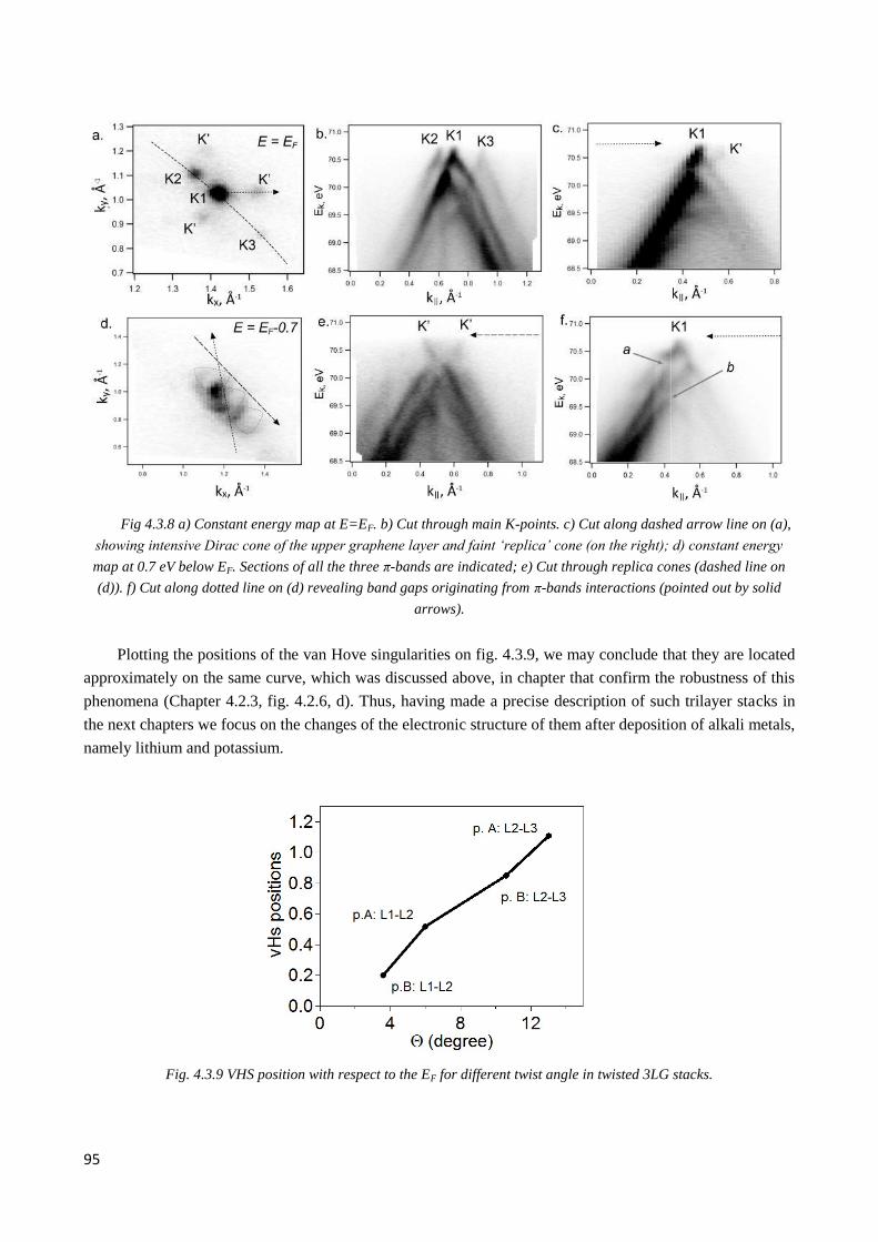
95
Fig 4.3.8 a) Constant energy map at E=EF. b) Cut through main K-points. c) Cut along dashed arrow line on (a),
showing intensive Dirac cone of the upper graphene layer and faint ‘replica’ cone (on the right); d) constant energy
map at 0.7 eV below EF. Sections of all the three π-bands are indicated; e) Cut through replica cones (dashed line on
(d)). f) Cut along dotted line on (d) revealing band gaps originating from π-bands interactions (pointed out by solid
arrows).
Plotting the positions of the van Hove singularities on fig. 4.3.9, we may conclude that they are located
approximately on the same curve, which was discussed above, in chapter that confirm the robustness of this
phenomena (Chapter 4.2.3, fig. 4.2.6, d). Thus, having made a precise description of such trilayer stacks in
the next chapters we focus on the changes of the electronic structure of them after deposition of alkali metals,
namely lithium and potassium.
Fig. 4.3.9 VHS position with respect to the EF for different twist angle in twisted 3LG stacks.
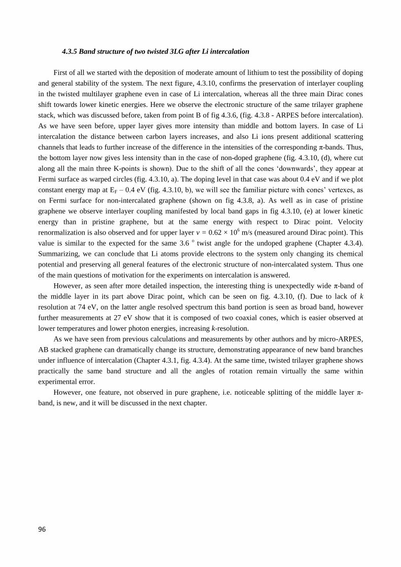
96
4.3.5 Band structure of two twisted 3LG after Li intercalation
First of all we started with the deposition of moderate amount of lithium to test the possibility of doping
and general stability of the system. The next figure, 4.3.10, confirms the preservation of interlayer coupling
in the twisted multilayer graphene even in case of Li intercalation, whereas all the three main Dirac cones
shift towards lower kinetic energies. Here we observe the electronic structure of the same trilayer graphene
stack, which was discussed before, taken from point B of fig 4.3.6, (fig. 4.3.8 - ARPES before intercalation).
As we have seen before, upper layer gives more intensity than middle and bottom layers. In case of Li
intercalation the distance between carbon layers increases, and also Li ions present additional scattering
channels that leads to further increase of the difference in the intensities of the corresponding π-bands. Thus,
the bottom layer now gives less intensity than in the case of non-doped graphene (fig. 4.3.10, (d), where cut
along all the main three K-points is shown). Due to the shift of all the cones ‘downwards’, they appear at
Fermi surface as warped circles (fig. 4.3.10, a). The doping level in that case was about 0.4 eV and if we plot
constant energy map at EF – 0.4 eV (fig. 4.3.10, b), we will see the familiar picture with cones’ vertexes, as
on Fermi surface for non-intercalated graphene (shown on fig 4.3.8, a). As well as in case of pristine
graphene we observe interlayer coupling manifested by local band gaps in fig 4.3.10, (e) at lower kinetic
energy than in pristine graphene, but at the same energy with respect to Dirac point. Velocity
renormalization is also observed and for upper layer v = 0.62 × 10⁶ m/s (measured around Dirac point). This
value is similar to the expected for the same 3.6 o twist angle for the undoped graphene (Chapter 4.3.4).
Summarizing, we can conclude that Li atoms provide electrons to the system only changing its chemical
potential and preserving all general features of the electronic structure of non-intercalated system. Thus one
of the main questions of motivation for the experiments on intercalation is answered.
However, as seen after more detailed inspection, the interesting thing is unexpectedly wide π-band of
the middle layer in its part above Dirac point, which can be seen on fig. 4.3.10, (f). Due to lack of k
resolution at 74 eV, on the latter angle resolved spectrum this band portion is seen as broad band, however
further measurements at 27 eV show that it is composed of two coaxial cones, which is easier observed at
lower temperatures and lower photon energies, increasing k-resolution.
As we have seen from previous calculations and measurements by other authors and by micro-ARPES,
AB stacked graphene can dramatically change its structure, demonstrating appearance of new band branches
under influence of intercalation (Chapter 4.3.1, fig. 4.3.4). At the same time, twisted trilayer graphene shows
practically the same band structure and all the angles of rotation remain virtually the same within
experimental error.
However, one feature, not observed in pure graphene, i.e. noticeable splitting of the middle layer π-
band, is new, and it will be discussed in the next chapter.
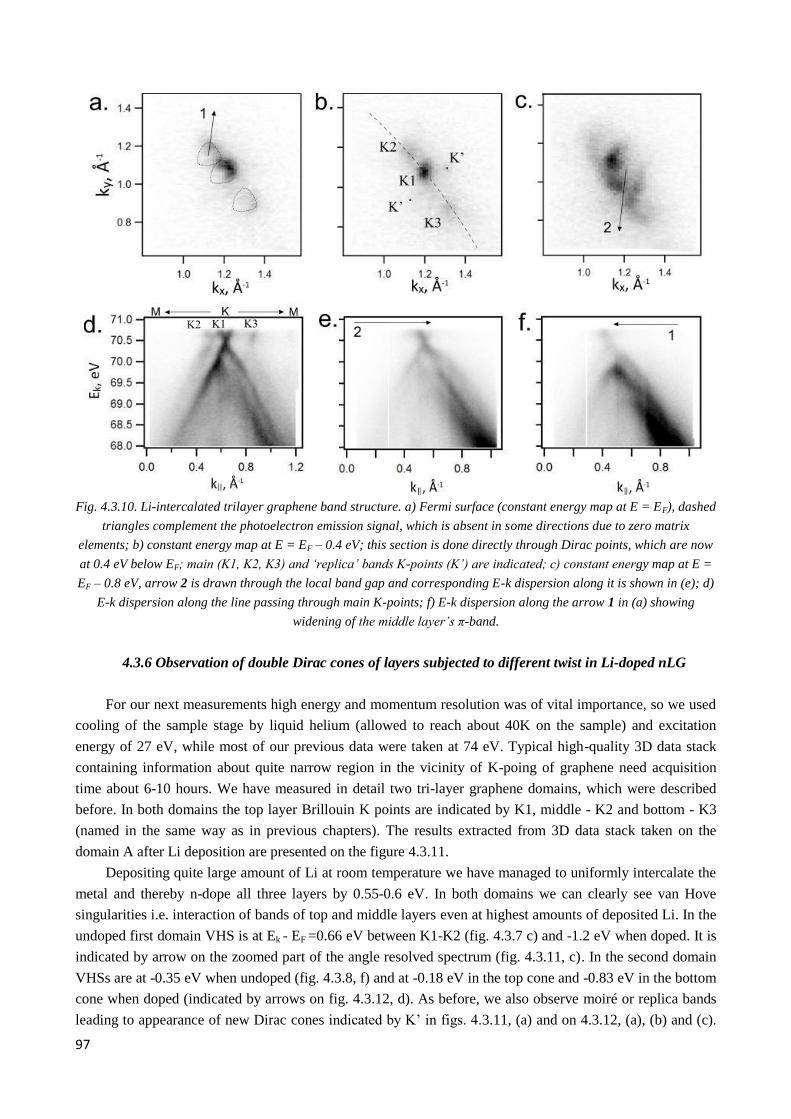
97
Fig. 4.3.10. Li-intercalated trilayer graphene band structure. a) Fermi surface (constant energy map at E = EF), dashed
triangles complement the photoelectron emission signal, which is absent in some directions due to zero matrix
elements; b) constant energy map at E = EF – 0.4 eV; this section is done directly through Dirac points, which are now
at 0.4 eV below EF; main (K1, K2, K3) and ‘replica’ bands K-points (K’) are indicated; c) constant energy map at E =
EF – 0.8 eV, arrow 2 is drawn through the local band gap and corresponding E-k dispersion along it is shown in (e); d)
E-k dispersion along the line passing through main K-points; f) E-k dispersion along the arrow 1 in (a) showing
widening of the middle layer’s π-band.
4.3.6 Observation of double Dirac cones of layers subjected to different twist in Li-doped nLG
For our next measurements high energy and momentum resolution was of vital importance, so we used
cooling of the sample stage by liquid helium (allowed to reach about 40K on the sample) and excitation
energy of 27 eV, while most of our previous data were taken at 74 eV. Typical high-quality 3D data stack
containing information about quite narrow region in the vicinity of K-poing of graphene need acquisition
time about 6-10 hours. We have measured in detail two tri-layer graphene domains, which were described
before. In both domains the top layer Brillouin K points are indicated by K1, middle - K2 and bottom - K3
(named in the same way as in previous chapters). The results extracted from 3D data stack taken on the
domain A after Li deposition are presented on the figure 4.3.11.
Depositing quite large amount of Li at room temperature we have managed to uniformly intercalate the
metal and thereby n-dope all three layers by 0.55-0.6 eV. In both domains we can clearly see van Hove
singularities i.e. interaction of bands of top and middle layers even at highest amounts of deposited Li. In the
undoped first domain VHS is at Ek - EF =0.66 eV between K1-K2 (fig. 4.3.7 c) and -1.2 eV when doped. It is
indicated by arrow on the zoomed part of the angle resolved spectrum (fig. 4.3.11, c). In the second domain
VHSs are at -0.35 eV when undoped (fig. 4.3.8, f) and at -0.18 eV in the top cone and -0.83 eV in the bottom
cone when doped (indicated by arrows on fig. 4.3.12, d). As before, we also observe moiré or replica bands
leading to appearance of new Dirac cones indicated by K’ in figs. 4.3.11, (a) and on 4.3.12, (a), (b) and (c).
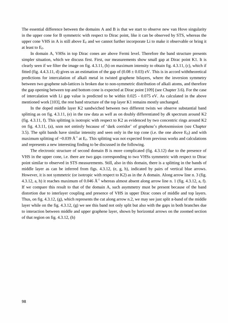
98
The essential difference between the domains A and B is that we start to observe new van Hove singularity
in the upper cone for B symmetric with respect to Dirac point, like it can be observed by STS, whereas the
upper cone VHS in A is still above EF and we cannot further incorporate Li to make it observable or bring it
at least to EF.
In domain A, VHSs in top Dirac cones are above Fermi level. Therefore the band structure presents
simpler situation, which we discuss first. First, our measurements show small gap at Dirac point K1. It is
clearly seen if we filter the image on fig. 4.3.11, (b) on maximum intensity to obtain fig. 4.3.11, (c), which if
fitted (fig. 4.4.3.11, d) gives us an estimation of the gap of (0.08 ± 0.03) eV. This is in accord withtheoretical
predictions for intercalation of alkali metal in twisted graphene bilayers, where the inversion symmetry
between two graphene sub-lattices is broken due to non-symmetric distribution of alkali atoms, and therefore
the gap opening between top and bottom cone is expected at Dirac point [109] (see Chapter 3.6). For the case
of intercalation with Li gap value is predicted to be within 0.025 - 0.075 eV. As calculated in the above
mentioned work [103], the rest band structure of the top layer K1 remains mostly unchanged.
In the doped middle layer K2 sandwiched between two different twists we observe substantial band
splitting as on fig. 4.3.11, (e) in the raw data as well as on doubly differentiated by dk spectrum around K2
(fig. 4.3.11, f). This splitting is isotropic with respect to K2 as evidenced by two concentric rings around K2
on fig. 4.3.11, (a), seen not entirely because of ‘dark corridor’ of graphene’s photoemission (see Chapter
3.5). The split bands have similar intensity and seen only in the top cone (i.e. the one above ED) and with
maximum splitting of ~0.039 Å-1
at EF. This splitting was not expected from previous works and calculations
and represents a new interesting finding to be discussed in the following.
The electronic structure of second domain B is more complicated (fig. 4.3.12) due to the presence of
VHS in the upper cone, i.e. there are two gaps corresponding to two VHSs symmetric with respect to Dirac
point similar to observed in STS measurements. Still, also in this domain, there is a splitting in the bands of
middle layer as can be inferred from figs. 4.3.12, (e, g, h), indicated by pairs of vertical blue arrows.
However, it is not symmetric (or isotropic with respect to K2) as in the A domain. Along arrow line n. 3 (fig.
4.3.12, a, h) it reaches maximum of 0.046 Å-1
whereas almost absent along arrow line n. 1 (fig. 4.3.12, a, f).
If we compare this result to that of the domain A, such asymmetry must be present because of the band
distortion due to interlayer coupling and presence of VHS in upper Dirac cones of middle and top layers.
Thus, on fig. 4.3.12, (g), which represents the cut along arrow n.2, we may see just split π-band of the middle
layer while on the fig. 4.3.12, (g) we see this band not only split but also with the gaps in both branches due
to interaction between middle and upper graphene layer, shown by horizontal arrows on the zoomed section
of that region on fig. 4.3.12, (h)
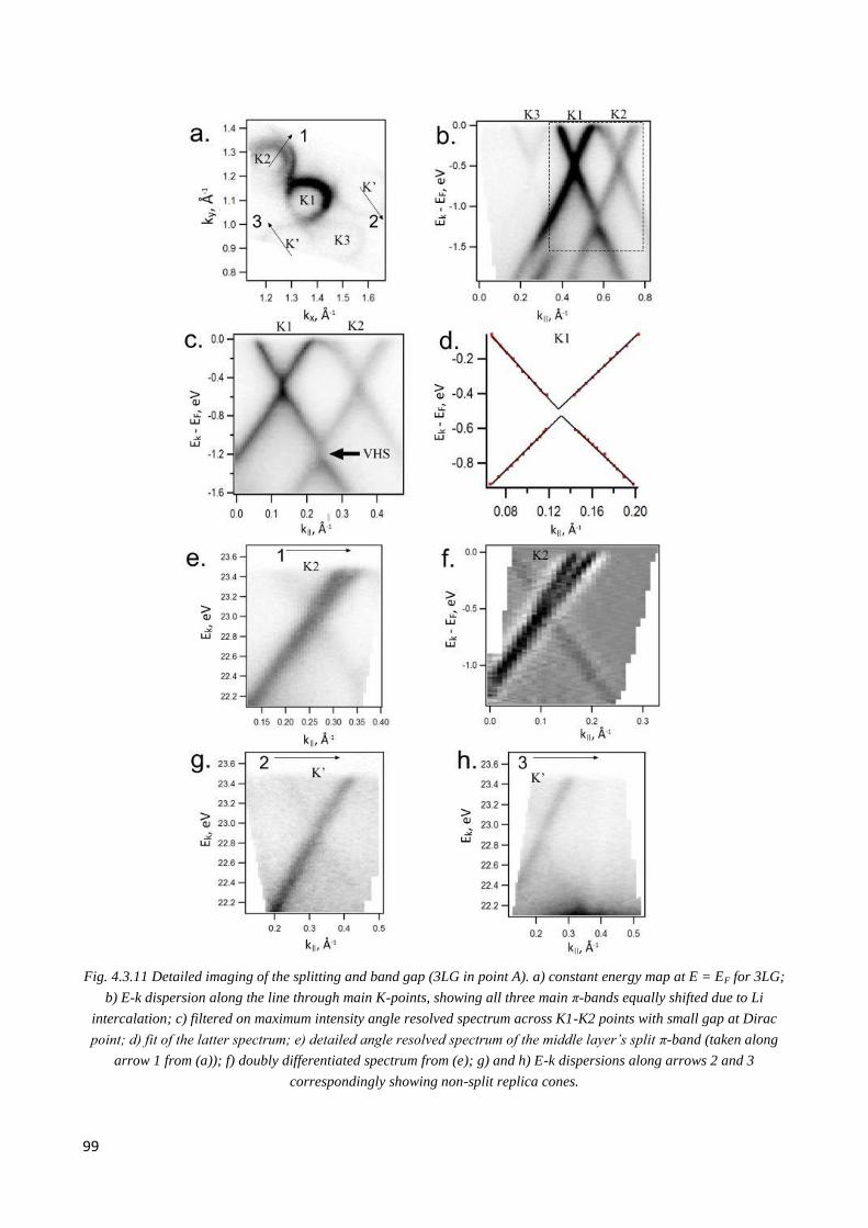
99
Fig. 4.3.11 Detailed imaging of the splitting and band gap (3LG in point A). a) constant energy map at E = EF for 3LG;
b) E-k dispersion along the line through main K-points, showing all three main π-bands equally shifted due to Li
intercalation; c) filtered on maximum intensity angle resolved spectrum across K1-K2 points with small gap at Dirac
point; d) fit of the latter spectrum; e) detailed angle resolved spectrum of the middle layer’s split π-band (taken along
arrow 1 from (a)); f) doubly differentiated spectrum from (e); g) and h) E-k dispersions along arrows 2 and 3
correspondingly showing non-split replica cones.
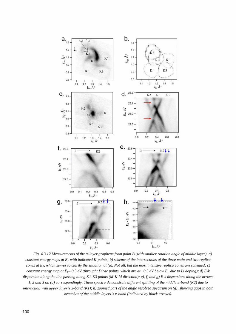
100
Fig. 4.3.12 Measurements of the trilayer graphene from point B (with smaller rotation angle of middle layer). a)
constant energy maps at EF with indicated K-points; b) scheme of the intersections of the three main and two replica
cones at EF, which serves to clarify the situation at (a). Not all, but the most intensive replica cones are schemed; c)
constant energy map at EF - 0.5 eV (throught Dirac points, which are at ~0.5 eV below EF due to Li doping); d) E-k
dispersion along the line passing along K1-K3 points (M-K-M direction); e), f) and g) E-k dispersions along the arrows
1, 2 and 3 on (a) correspondingly. These spectra demonstrate different splitting of the middle π-band (K2) due to
interaction with upper layer’s π-band (K1); h) zoomed part of the angle resolved spectrum on (g), showing gaps in both
branches of the middle layers’s π-band (indicated by black arrows).
101
The split bands at K2 in both cases cannot be superposition of two spatially separated domains as we
have done several experiments with cleaning and redepositing and each time the results including the
intensity ratio between branches of the split band remains the same (1:1). Most importantly, there is clearly
visible asymmetry between upper and lower cones for both domains evidenced in fig. 4.3.11, (f), and also the
slope, i.e. group velosities of charge carriers in two branches are different, and therefore the separation
between the bands increase with increase of the energy with respect to ED.
By the appearance and equal intensity in the split bands the splitting resembles mostly Rashba-type if
we compare it to other well-known systems [143]. However, the "classical" Rashba splitting is difficult to
accept because SO coupling in graphene is small [144] due to inversion symmetry and also light Li atoms
should not enhance it as, for example, atoms of gold were suggested to do [143].
Fig. 4.3.13 Splitting of the bands in doped multilayer graphene. a) Band structure of a twisted (9°) bilayer graphene
intercalated with one Ca atom per unit cell (inset without intercalation) [109]; b) zoomed part of the image (a) with
arrows indicating the clearly double π-band above Dirac point and single below; c) Calculated band structure of AA-
stacked C6LiC6. (b) and (c) adopted from [139] d) Experimental observation of band splitting for twisted Li-intercalated
3LG.
Some calculations for doped bilayer graphene resemble the band structure that we see in our case. First
of all the calculations by N. M. Caffrey et al. of the Li-doped AA-stacked bilayer show that one of the π-
bands become doubled, while the other becomes single (fig. 4.3.13, c) that is similar to what we see,
although we have another type of stacking [139]. Another work dealing with doped twisted bilayer graphene,
also shows some similar results [109], that was already mentioned in the review part of the thesis (section
3.6). Fig. 4.3.13, (a) and (b) from paper by F. Symalla et al. shows band structure around K-point for twisted
bilayer graphene (angle of misorientation 9°). In case of pristine graphene Dirac point is at EF and a single
band observed near it, while for Ca-doped system the band splitting can be seen as well as Fermi level shift
and band gap creation. Two branches indicated by arrows on fig. 4.3.13, (b) demonstrate observable splitting
above Dirac point while it goes to zero in the lower part of the π-band. Similar, but much stronger non-
uniform character of splitting we see in our system: it is bigger for upper Dirac cone, reaching 0.035 Å-1
at
EF, and hard to be resolved below Dirac point (shown in fig. 4.3.13, d). Figs. 4.3.13, (b) and (c) represent Li-
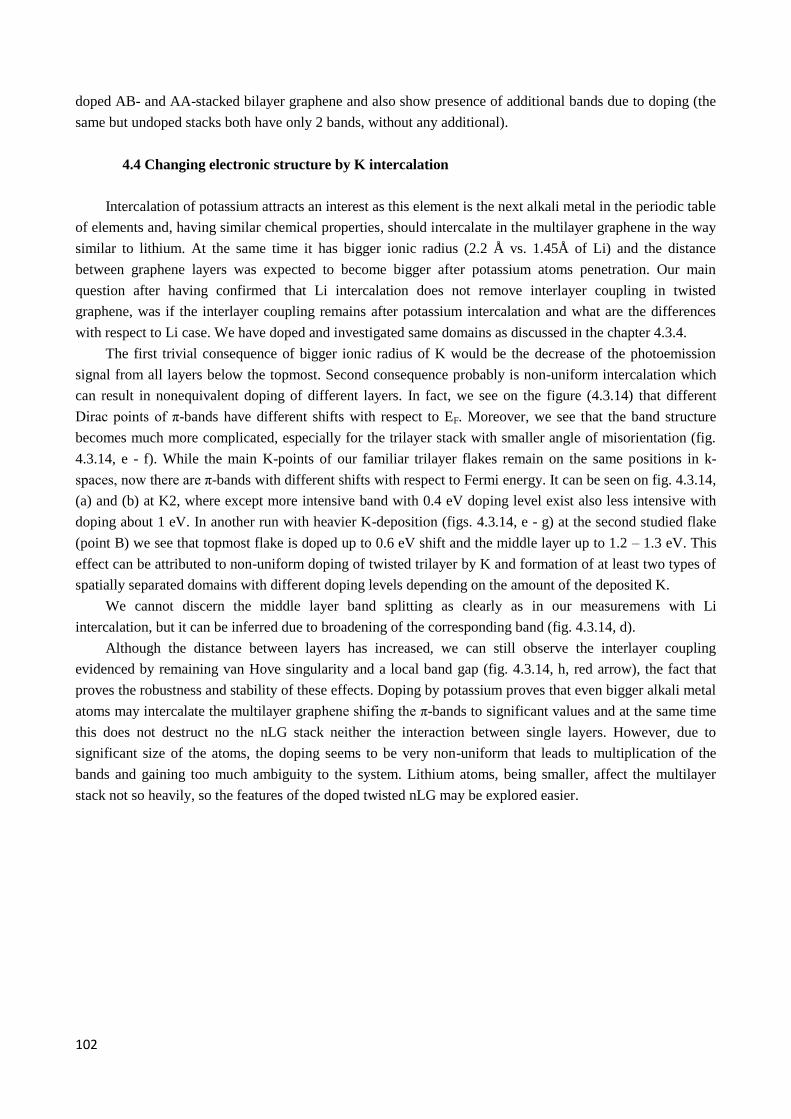
102
doped AB- and AA-stacked bilayer graphene and also show presence of additional bands due to doping (the
same but undoped stacks both have only 2 bands, without any additional).
4.4 Changing electronic structure by K intercalation
Intercalation of potassium attracts an interest as this element is the next alkali metal in the periodic table
of elements and, having similar chemical properties, should intercalate in the multilayer graphene in the way
similar to lithium. At the same time it has bigger ionic radius (2.2 Å vs. 1.45Å of Li) and the distance
between graphene layers was expected to become bigger after potassium atoms penetration. Our main
question after having confirmed that Li intercalation does not remove interlayer coupling in twisted
graphene, was if the interlayer coupling remains after potassium intercalation and what are the differences
with respect to Li case. We have doped and investigated same domains as discussed in the chapter 4.3.4.
The first trivial consequence of bigger ionic radius of K would be the decrease of the photoemission
signal from all layers below the topmost. Second consequence probably is non-uniform intercalation which
can result in nonequivalent doping of different layers. In fact, we see on the figure (4.3.14) that different
Dirac points of π-bands have different shifts with respect to EF. Moreover, we see that the band structure
becomes much more complicated, especially for the trilayer stack with smaller angle of misorientation (fig.
4.3.14, e - f). While the main K-points of our familiar trilayer flakes remain on the same positions in k-
spaces, now there are π-bands with different shifts with respect to Fermi energy. It can be seen on fig. 4.3.14,
(a) and (b) at K2, where except more intensive band with 0.4 eV doping level exist also less intensive with
doping about 1 eV. In another run with heavier K-deposition (figs. 4.3.14, e - g) at the second studied flake
(point B) we see that topmost flake is doped up to 0.6 eV shift and the middle layer up to 1.2 – 1.3 eV. This
effect can be attributed to non-uniform doping of twisted trilayer by K and formation of at least two types of
spatially separated domains with different doping levels depending on the amount of the deposited K.
We cannot discern the middle layer band splitting as clearly as in our measuremens with Li
intercalation, but it can be inferred due to broadening of the corresponding band (fig. 4.3.14, d).
Although the distance between layers has increased, we can still observe the interlayer coupling
evidenced by remaining van Hove singularity and a local band gap (fig. 4.3.14, h, red arrow), the fact that
proves the robustness and stability of these effects. Doping by potassium proves that even bigger alkali metal
atoms may intercalate the multilayer graphene shifing the π-bands to significant values and at the same time
this does not destruct no the nLG stack neither the interaction between single layers. However, due to
significant size of the atoms, the doping seems to be very non-uniform that leads to multiplication of the
bands and gaining too much ambiguity to the system. Lithium atoms, being smaller, affect the multilayer
stack not so heavily, so the features of the doped twisted nLG may be explored easier.
103
Fig. 4.3.14 Band structure change after potassium intercalation in trilayer graphene. a), e) constant energy map at E =
EF for graphene flakes A and B correspondingly; b) constant energy map at E = EF – 0.25 eV; c), g) slice in KMK
direction in the vicinity of K-points of trilayer stacks in points A and B correspondingly; d) cut along arrow from (a)
showing middle layer π-band in details; h) topmost layer’s π-band with van Hove singularity.
104
4.5 Chapter summary
We successfully managed to intercalate alkali metals into twisted graphene domains and study several
interesting configurations using µ-ARPES, concentrating our efforts again on physics of twisted trilayers.
First result is clear evidence that intercalation of the alkali metals into twisted graphene does not
remove interlayer coupling between graphene layers. We have seen the robustness of VHSs for both metals
employed by us, Li and K. The difference is that Li, being lighter, intercalates more uniformly and provides
uniform doping in twisted graphene, and therefore is more suitable model system. The natural consequence
of the robustness of VHS in doped graphene is the possibility of obtaining one quasi- one- dimensional
transport discussed in 4.2.6 by careful adjustment of the dopant concentration. It should be noted however
that in case of alkali dopant, producing always n-type doping and shifting Dirac point below EF, one must
seek to stabilize the top cone VHS at EF.
Secondly, the predicted by calculations effect of small gap between Dirac cones of K point, is observed
by us and is of the order of 70 meV in case of Li intercalation in twisted graphene. This gap is due to
symmetry breaking in graphene sublattice induced by the electric field of Li ions, nonuniformly distributed
in the potential Moiré lattice of twisted graphene.
Third the most striking observation is again related to poorly explored physics of trilayes of twisted
graphene and to most probably symmetry breaking of its sublattices: the clear evidence of giant splitting of
π-bands of upper Dirac cone of the middle layer, subjected to different twists on its two sides. This result has
not been predicted but it should be admitted also that the system has not been studied up to now
theoretically.
In fact, the role of Li should be carefully verified, if the splitting is present on the upper cones, not seen
by us in undoped samples or it is the electric field of Li ions which causes the splitting. In fact much smaller
splitting is observed already in caclulations of twisted intercalated bilayers but no attention is paid to it in the
discussion of the paper (chapter 4.3.6, [103]).
Equal intensity of both branches would be the evidence of Rashba-type splitting. As it was mentioned
before, this cannot be due to graphene’s intrinsic spin-orbit coupling neither the one induced by lithium or
potassium, because these ones give only some μeV’s of the distance between branches, while here we have
2-3 orders of magnitude more. This can be related to the presence of electric field, caused by non-locally
uniformly intercalated lithium atoms and pseudospin splitting due to this field. The magnitude of the electric
field differs in examined regions A and B as the different twists anticipate different unit cell size and
correspondingly different number of lithium/potassium atoms per unit cell which can be intercalated. Thus
we see slightly different value of the splitting in these two stacks. In the first one (A) it is about 0.039 Å at
EF. In the second one (B) it is non-uniform, because of the distortion caused by interlayer coupling and
maximum distance is ~0.05 Å.
Underlining once again that it is not possible to observe top cone of Dirac spectrum by µ-ARPES
without introducing Li, and therefore theoretical efforts or more sophisticated experiments such as gating by
electric fields are needed to disentangle the effects of Li ions and different twist Moiré patterns on the two
sides of middle layer graphene in tri layer twisted graphene stack, we mention below several works which
are related to pseudo-spintronics of graphene and so called pseudo-spin Rashba splitting and some analogies
in physics since the spectrum of middle layer is reminding us Rashba splitting.
In fact the spin is quantized intrinsic angular momentum of a particle, however many other material
properties can act as an effective spin of ±1/2 [145]. It has been employed even in the physics of ultra-cold
atoms to describe two atomic hyperfine states in laser field, leading to pseudo-spin coupling and Rashba -like
dispersion [146]. In hexagonal 2D materials, like graphene, the pseudo-spin can be composed of two
105
sublattices [147]. On the contrary to small spin-orbit coupling the pseudospin-orbit coupling in graphene is
large or even very strong with electrostatic field acting as the analogue to magnetic field in classic Rashba
effect [66]. The main most important difference is that pseudo-spin has only significance inside the material
(graphene), since the charge carrier leaving it via the contact does not have any more pseudo-spin property,
which naturally limits the applications. Interestingly, however, that also the layer number can be treated as
pseudospin in multilayer system. In this case this value is even easier to manipulate and bilayer graphene
pseudospin-valve devices have been suggested [148].
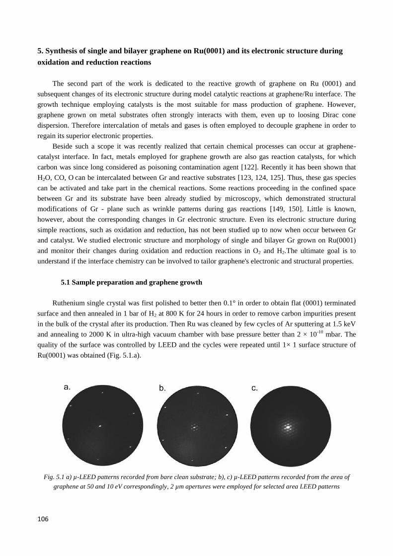
106
5. Synthesis of single and bilayer graphene on Ru(0001) and its electronic structure during
oxidation and reduction reactions
The second part of the work is dedicated to the reactive growth of graphene on Ru (0001) and
subsequent changes of its electronic structure during model catalytic reactions at graphene/Ru interface. The
growth technique employing catalysts is the most suitable for mass production of graphene. However,
graphene grown on metal substrates often strongly interacts with them, even up to loosing Dirac cone
dispersion. Therefore intercalation of metals and gases is often employed to decouple graphene in order to
regain its superior electronic properties.
Beside such a scope it was recently realized that certain chemical processes can occur at graphene-
catalyst interface. In fact, metals employed for graphene growth are also gas reaction catalysts, for which
carbon was since long considered as poisoning contamination agent [122]. Recently it has been shown that
H2O, CO, O can be intercalated between Gr and reactive substrates [123, 124, 125]. Thus, these gas species
can be activated and take part in the chemical reactions. Some reactions proceeding in the confined space
between Gr and its substrate have been already studied by microscopy, which demonstrated structural
modifications of Gr - plane such as wrinkle patterns during gas reactions [149, 150]. Little is known,
however, about the corresponding changes in Gr electronic structure. Even its electronic structure during
simple reactions, such as oxidation and reduction, has not been studied up to now when occur between Gr
and catalyst. We studied electronic structure and morphology of single and bilayer Gr grown on Ru(0001)
and monitor their changes during oxidation and reduction reactions in O2 and H2.The ultimate goal is to
understand if the interface chemistry can be involved to tailor graphene's electronic and structural properties.
5.1 Sample preparation and graphene growth
Ruthenium single crystal was first polished to better then 0.1° in order to obtain flat (0001) terminated
surface and then annealed in 1 bar of H2 at 800 K for 24 hours in order to remove carbon impurities present
in the bulk of the crystal after its production. Then Ru was cleaned by few cycles of Ar sputtering at 1.5 keV
and annealing to 2000 K in ultra-high vacuum chamber with base pressure better than 2 × 10⁻¹⁰
mbar. The
quality of the surface was controlled by LEED and the cycles were repeated until 1× 1 surface structure of
Ru(0001) was obtained (Fig. 5.1.a).
Fig. 5.1 a) µ-LEED patterns recorded from bare clean substrate; b), c) µ-LEED patterns recorded from the area of
graphene at 50 and 10 eV correspondingly, 2 µm apertures were employed for selected area LEED patterns
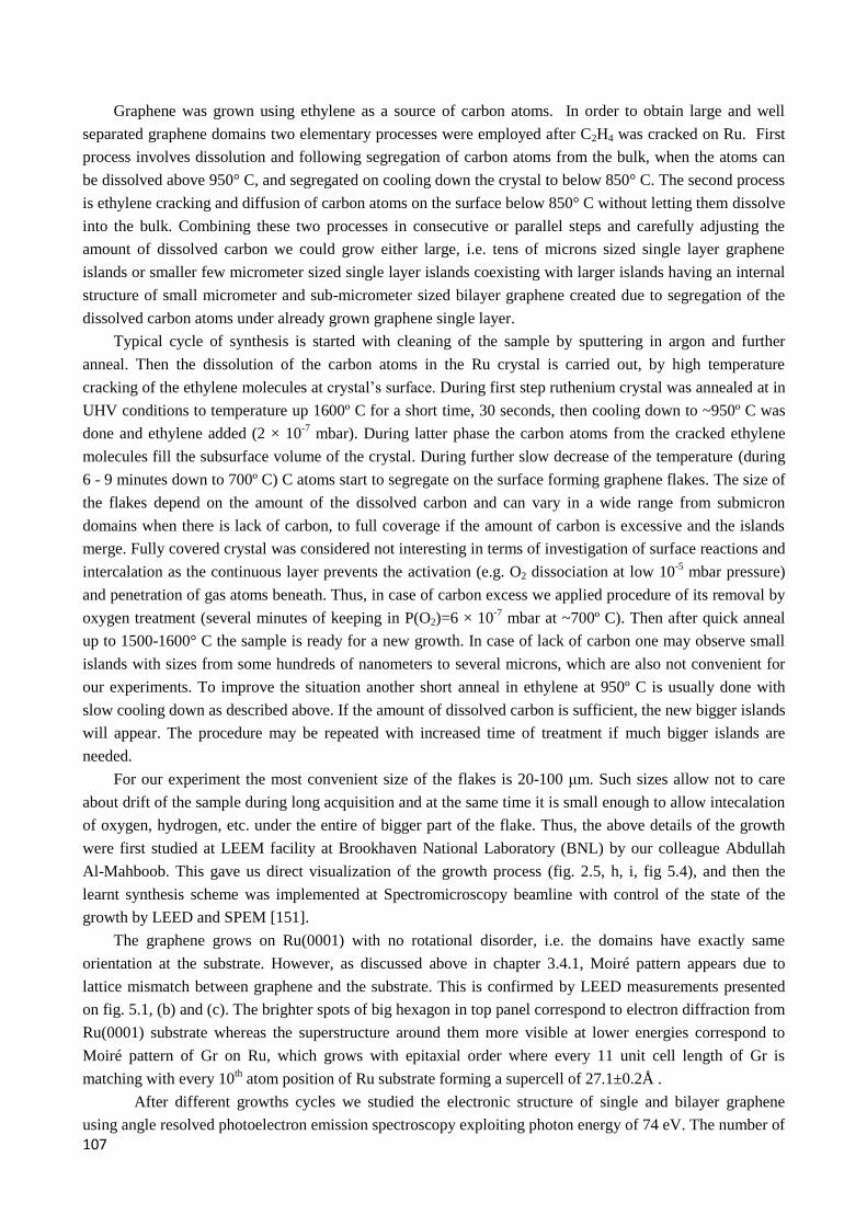
107
Graphene was grown using ethylene as a source of carbon atoms. In order to obtain large and well
separated graphene domains two elementary processes were employed after C2H4 was cracked on Ru. First
process involves dissolution and following segregation of carbon atoms from the bulk, when the atoms can
be dissolved above 950° C, and segregated on cooling down the crystal to below 850° C. The second process
is ethylene cracking and diffusion of carbon atoms on the surface below 850° C without letting them dissolve
into the bulk. Combining these two processes in consecutive or parallel steps and carefully adjusting the
amount of dissolved carbon we could grow either large, i.e. tens of microns sized single layer graphene
islands or smaller few micrometer sized single layer islands coexisting with larger islands having an internal
structure of small micrometer and sub-micrometer sized bilayer graphene created due to segregation of the
dissolved carbon atoms under already grown graphene single layer.
Typical cycle of synthesis is started with cleaning of the sample by sputtering in argon and further
anneal. Then the dissolution of the carbon atoms in the Ru crystal is carried out, by high temperature
cracking of the ethylene molecules at crystal’s surface. During first step ruthenium crystal was annealed at in
UHV conditions to temperature up 1600º C for a short time, 30 seconds, then cooling down to ~950º C was
done and ethylene added (2 × 10⁻⁷
mbar). During latter phase the carbon atoms from the cracked ethylene
molecules fill the subsurface volume of the crystal. During further slow decrease of the temperature (during
6 - 9 minutes down to 700º C) C atoms start to segregate on the surface forming graphene flakes. The size of
the flakes depend on the amount of the dissolved carbon and can vary in a wide range from submicron
domains when there is lack of carbon, to full coverage if the amount of carbon is excessive and the islands
merge. Fully covered crystal was considered not interesting in terms of investigation of surface reactions and
intercalation as the continuous layer prevents the activation (e.g. O2 dissociation at low 10-5
mbar pressure)
and penetration of gas atoms beneath. Thus, in case of carbon excess we applied procedure of its removal by
oxygen treatment (several minutes of keeping in P(O2)=6 × 10⁻⁷
mbar at ~700º C). Then after quick anneal
up to 1500-1600° C the sample is ready for a new growth. In case of lack of carbon one may observe small
islands with sizes from some hundreds of nanometers to several microns, which are also not convenient for
our experiments. To improve the situation another short anneal in ethylene at 950º C is usually done with
slow cooling down as described above. If the amount of dissolved carbon is sufficient, the new bigger islands
will appear. The procedure may be repeated with increased time of treatment if much bigger islands are
needed.
For our experiment the most convenient size of the flakes is 20-100 μm. Such sizes allow not to care
about drift of the sample during long acquisition and at the same time it is small enough to allow intecalation
of oxygen, hydrogen, etc. under the entire of bigger part of the flake. Thus, the above details of the growth
were first studied at LEEM facility at Brookhaven National Laboratory (BNL) by our colleague Abdullah
Al-Mahboob. This gave us direct visualization of the growth process (fig. 2.5, h, i, fig 5.4), and then the
learnt synthesis scheme was implemented at Spectromicroscopy beamline with control of the state of the
growth by LEED and SPEM [151].
The graphene grows on Ru(0001) with no rotational disorder, i.e. the domains have exactly same
orientation at the substrate. However, as discussed above in chapter 3.4.1, Moiré pattern appears due to
lattice mismatch between graphene and the substrate. This is confirmed by LEED measurements presented
on fig. 5.1, (b) and (c). The brighter spots of big hexagon in top panel correspond to electron diffraction from
Ru(0001) substrate whereas the superstructure around them more visible at lower energies correspond to
Moiré pattern of Gr on Ru, which grows with epitaxial order where every 11 unit cell length of Gr is
matching with every 10th atom position of Ru substrate forming a supercell of 27.1±0.2Å .
After different growths cycles we studied the electronic structure of single and bilayer graphene
using angle resolved photoelectron emission spectroscopy exploiting photon energy of 74 eV. The number of
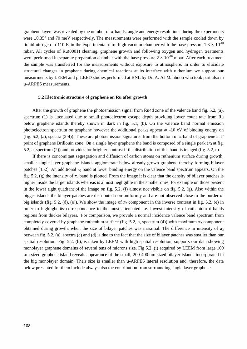
108
graphene layers was revealed by the number of π-bands, angle and energy resolutions during the experiments
were ±0.35° and 70 meV respectively. The measurements were performed with the sample cooled down by
liquid nitrogen to 110 K in the experimental ultra-high vacuum chamber with the base pressure 1.3 × 10⁻¹⁰
mbar. All cycles of Ru(0001) cleaning, graphene growth and following oxygen and hydrogen treatments
were performed in separate preparation chamber with the base pressure 2 × 10⁻¹⁰
mbar. After each treatment
the sample was transferred for the measurements without exposure to atmosphere. In order to elucidate
structural changes in graphene during chemical reactions at its interface with ruthenium we support our
measurments by LEEM and µ-LEED studies performed at BNL by Dr. A. Al-Mahboob who took part also in
µ-ARPES measurements.
5.2 Electronic structure of graphene on Ru after growth
After the growth of graphene the photoemission signal from Ru4d zone of the valence band fig. 5.2, (a),
spectrum (1) is attenuated due to small photoelectron escape depth providing lower count rate from Ru
below graphene islands thereby shown in dark in fig. 5.1, (b). On the valence band normal emission
photoelectron spectrum on graphene however the additional peaks appear at -10 eV of binding energy on
(fig. 5.2, (a), spectra (2-4)). These are photoemission signatures from the bottom of π-band of graphene at Γ
point of graphene Brillouin zone. On a single layer graphene the band is composed of a single peak (π1 at fig.
5.2, a, spectrum (2)) and provides for brighter contrast if the distribution of this band is imaged (fig. 5.2, c).
If there is concomitant segregation and diffusion of carbon atoms on ruthenium surface during growth,
smaller single layer graphene islands agglomerate below already grown graphene thereby forming bilayer
patches [152]. An additional π2 band at lower binding energy on the valence band spectrum appears. On the
fig. 5.2, (g) the intensity of π2 band is plotted. From the image it is clear that the density of bilayer patches is
higher inside the larger islands whereas is almost negligible in the smaller ones, for example on those present
in the lower right quadrant of the image on fig. 5.2, (f) almost not visible on fig. 5.2, (g). Also within the
bigger islands the bilayer patches are distributed non-uniformly and are not observed close to the border of
big islands (fig. 5.2, (d), (e)). We show the image of π2 component in the inverse contrast in fig. 5.2, (e) in
order to highlight its correspondence to the most attenuated i.e. lowest intensity of ruthenium d-bands
regions from thicker bilayers. For comparison, we provide a normal incidence valence band spectrum from
completely covered by graphene ruthenium surface (fig. 5.2, a, spectrum (4)) with maximum π2 component
obtained during growth, when the size of bilayer patches was maximal. The difference in intensity of π2
between fig. 5.2, (a), spectra (c) and (d) is due to the fact that the size of bilayer patches was smaller than our
spatial resolution. Fig. 5.2, (h), is taken by LEEM with high spatial resolution, supports our data showing
monolayer graphene domains of several tens of microns size. Fig 5.2, (i) acquired by LEEM from large 100
µm sized graphene island reveals appearance of the small, 200-400 nm-sized bilayer islands incorporated in
the big monolayer domain. Their size is smaller than µ-ARPES lateral resolution and, therefore, the data
below presented for them include always also the contribution from surrounding single layer graphene.
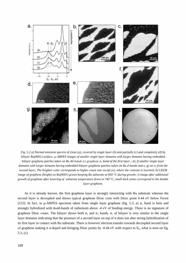
109
Fig. 5.2 a) Normal emission spectra of clean (a), covered by single layer (b) and partially (c) and completely (d) by
bilayer Ru(0001) surface; µ-ARPES images of smaller single layer domains with larger domains having embedded
bilayer graphene patches taken on Ru 4d-bands (c) graphene π1 band of the first layer ; d), f) smaller single layer
domains with larger domains having embedded bilayer graphene patches taken on Ru d-bands and e, g) on π2 from the
second layer; The brighter color corresponds to higher count rate except (e), where the contrast is inverted; h) LEEM
image of graphene (bright) on Ru(0001) grown keeping Ru substrate at 850 °C during growth; i) image after additional
growth of graphene after lowering of substrate temperature down to 740 °C, small dark zones correspond to the double
layer graphene.
As it is already known, the first graphene layer is strongly interacting with Ru substrate whereas the
second layer is decoupled and shows typical graphene Dirac cone with Dirac point 0.44 eV below Fermi
[153]. In fact, in µ-ARPES spectrum taken from single layer graphene (fig. 5.3, a) π1 band is bent and
strongly hybridized with Ru4d-bands of ruthenium above -4 eV of binding energy. There is no signature of
graphene Dirac cones. The bilayer shows both π1 and 𝜋2 bands. π1 of bilayer is very similar to the single
layer domains indicating that the presence of a second layer on top of it does not alter strong hybridization of
its first layer in contact with Ru substrate. There is however electron transfer towards decoupled second layer
of graphene making it n-doped and bringing Dirac points by -0.44 eV with respect to EF, what is seen on fig.
5.3, (c).
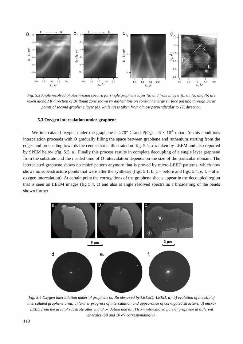
110
Fig. 5.3 Angle resolved photoemission spectra for single graphene layer (a) and from bilayer (b, c). (a) and (b) are
taken along ΓK direction of Brillouin zone shown by dashed line on constant energy surface passing through Dirac
points of second graphene layer (d), while (c) is taken from almost perpendicular to ΓK direction.
5.3 Oxygen intercalation under graphene
We intercalated oxygen under the graphene at 270° C and P(O2) = 6 × 10⁻⁶
mbar. At this conditions
intercalation proceeds with O gradually filling the space between graphene and ruthenium starting from the
edges and proceeding towards the center that is illustrated on fig. 5.4, x-x taken by LEEM and also reported
by SPEM below (fig. 5.5, a). Finally this process results in complete decoupling of a single layer graphene
from the substrate and the needed time of O-intercalation depends on the size of the particular domain. The
intercalated graphene shows no moiré pattern anymore that is proved by micro-LEED patterns, which now
shows no superstructure points that were after the synthesis (figs. 5.1, b, c – before and figs. 5.4, e, f. – after
oxygen intercalation). At certain point the corrugations of the graphene sheets appear in the decoupled region
that is seen on LEEM images (fig 5.4, c) and also at angle resolved spectra as a broadening of the bands
shown further.
Fig. 5.4 Oxygen intercalation under of graphene on Ru observed by LEEM/μ-LEED. a), b) evolution of the size of
intercalated graphene area; c) further progress of intercalation and appearance of corrugated structure; d) micro-
LEED from the area of substrate after end of oxidation and e), f) from intercalated part of graphene at different
energies (50 and 10 eV correspondingly).
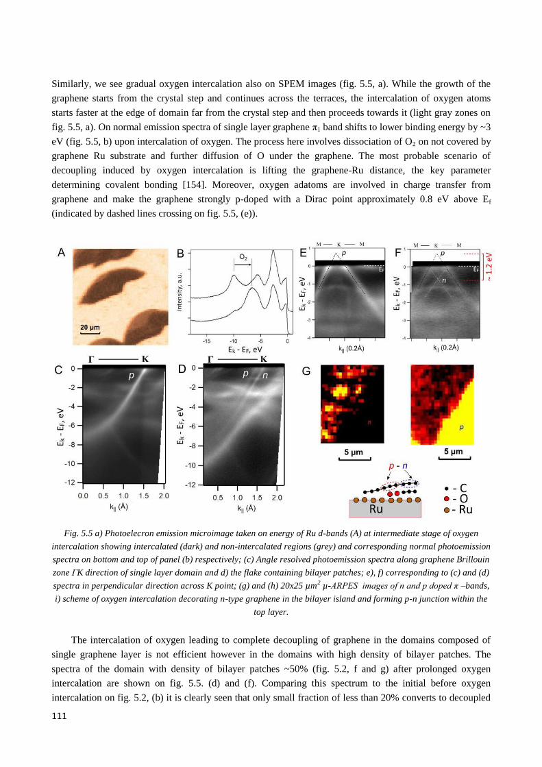
111
Similarly, we see gradual oxygen intercalation also on SPEM images (fig. 5.5, a). While the growth of the
graphene starts from the crystal step and continues across the terraces, the intercalation of oxygen atoms
starts faster at the edge of domain far from the crystal step and then proceeds towards it (light gray zones on
fig. 5.5, a). On normal emission spectra of single layer graphene π1 band shifts to lower binding energy by ~3
eV (fig. 5.5, b) upon intercalation of oxygen. The process here involves dissociation of O2 on not covered by
graphene Ru substrate and further diffusion of O under the graphene. The most probable scenario of
decoupling induced by oxygen intercalation is lifting the graphene-Ru distance, the key parameter
determining covalent bonding [154]. Moreover, oxygen adatoms are involved in charge transfer from
graphene and make the graphene strongly p-doped with a Dirac point approximately 0.8 eV above Ef
(indicated by dashed lines crossing on fig. 5.5, (e)).
Fig. 5.5 a) Photoelecron emission microimage taken on energy of Ru d-bands (A) at intermediate stage of oxygen
intercalation showing intercalated (dark) and non-intercalated regions (grey) and corresponding normal photoemission
spectra on bottom and top of panel (b) respectively; (c) Angle resolved photoemission spectra along graphene Brillouin
zone ΓK direction of single layer domain and d) the flake containing bilayer patches; e), f) corresponding to (c) and (d)
spectra in perpendicular direction across K point; (g) and (h) 20x25 µm2 µ-ARPES images of n and p doped π –bands,
i) scheme of oxygen intercalation decorating n-type graphene in the bilayer island and forming p-n junction within the
top layer.
The intercalation of oxygen leading to complete decoupling of graphene in the domains composed of
single graphene layer is not efficient however in the domains with high density of bilayer patches. The
spectra of the domain with density of bilayer patches ~50% (fig. 5.2, f and g) after prolonged oxygen
intercalation are shown on fig. 5.5. (d) and (f). Comparing this spectrum to the initial before oxygen
intercalation on fig. 5.2, (b) it is clearly seen that only small fraction of less than 20% converts to decoupled
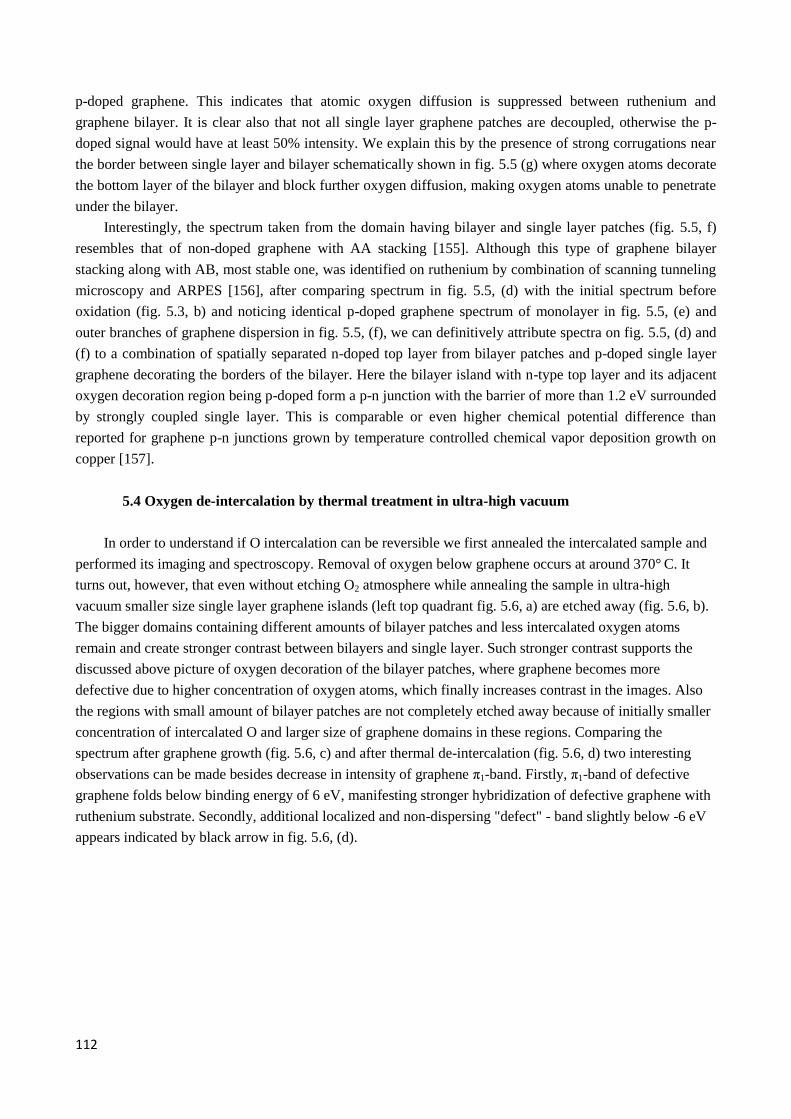
112
p-doped graphene. This indicates that atomic oxygen diffusion is suppressed between ruthenium and
graphene bilayer. It is clear also that not all single layer graphene patches are decoupled, otherwise the p-
doped signal would have at least 50% intensity. We explain this by the presence of strong corrugations near
the border between single layer and bilayer schematically shown in fig. 5.5 (g) where oxygen atoms decorate
the bottom layer of the bilayer and block further oxygen diffusion, making oxygen atoms unable to penetrate
under the bilayer.
Interestingly, the spectrum taken from the domain having bilayer and single layer patches (fig. 5.5, f)
resembles that of non-doped graphene with AA stacking [155]. Although this type of graphene bilayer
stacking along with AB, most stable one, was identified on ruthenium by combination of scanning tunneling
microscopy and ARPES [156], after comparing spectrum in fig. 5.5, (d) with the initial spectrum before
oxidation (fig. 5.3, b) and noticing identical p-doped graphene spectrum of monolayer in fig. 5.5, (e) and
outer branches of graphene dispersion in fig. 5.5, (f), we can definitively attribute spectra on fig. 5.5, (d) and
(f) to a combination of spatially separated n-doped top layer from bilayer patches and p-doped single layer
graphene decorating the borders of the bilayer. Here the bilayer island with n-type top layer and its adjacent
oxygen decoration region being p-doped form a p-n junction with the barrier of more than 1.2 eV surrounded
by strongly coupled single layer. This is comparable or even higher chemical potential difference than
reported for graphene p-n junctions grown by temperature controlled chemical vapor deposition growth on
copper [157].
5.4 Oxygen de-intercalation by thermal treatment in ultra-high vacuum
In order to understand if O intercalation can be reversible we first annealed the intercalated sample and
performed its imaging and spectroscopy. Removal of oxygen below graphene occurs at around 370° C. It
turns out, however, that even without etching O2 atmosphere while annealing the sample in ultra-high
vacuum smaller size single layer graphene islands (left top quadrant fig. 5.6, a) are etched away (fig. 5.6, b).
The bigger domains containing different amounts of bilayer patches and less intercalated oxygen atoms
remain and create stronger contrast between bilayers and single layer. Such stronger contrast supports the
discussed above picture of oxygen decoration of the bilayer patches, where graphene becomes more
defective due to higher concentration of oxygen atoms, which finally increases contrast in the images. Also
the regions with small amount of bilayer patches are not completely etched away because of initially smaller
concentration of intercalated O and larger size of graphene domains in these regions. Comparing the
spectrum after graphene growth (fig. 5.6, c) and after thermal de-intercalation (fig. 5.6, d) two interesting
observations can be made besides decrease in intensity of graphene π1-band. Firstly, π1-band of defective
graphene folds below binding energy of 6 eV, manifesting stronger hybridization of defective graphene with
ruthenium substrate. Secondly, additional localized and non-dispersing "defect" - band slightly below -6 eV
appears indicated by black arrow in fig. 5.6, (d).
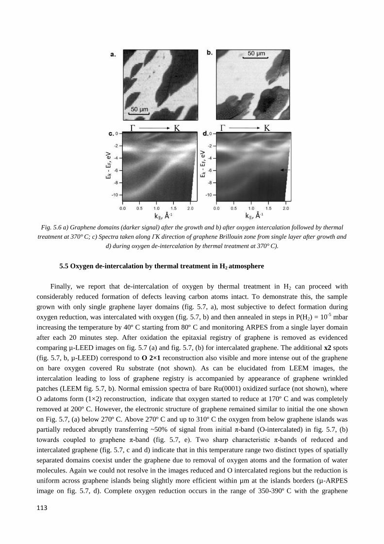
113
Fig. 5.6 a) Graphene domains (darker signal) after the growth and b) after oxygen intercalation followed by thermal
treatment at 370° C; c) Spectra taken along ΓK direction of graphene Brillouin zone from single layer after growth and
d) during oxygen de-intercalation by thermal treatment at 370° C).
5.5 Oxygen de-intercalation by thermal treatment in H2 atmosphere
Finally, we report that de-intercalation of oxygen by thermal treatment in H2 can proceed with
considerably reduced formation of defects leaving carbon atoms intact. To demonstrate this, the sample
grown with only single graphene layer domains (fig. 5.7, a), most subjective to defect formation during
oxygen reduction, was intercalated with oxygen (fig. 5.7, b) and then annealed in steps in P(H2) = 10-5
mbar
increasing the temperature by 40º C starting from 80º C and monitoring ARPES from a single layer domain
after each 20 minutes step. After oxidation the epitaxial registry of graphene is removed as evidenced
comparing µ-LEED images on fig. 5.7 (a) and fig. 5.7, (b) for intercalated graphene. The additional x2 spots
(fig. 5.7, b, µ-LEED) correspond to O 2×1 reconstruction also visible and more intense out of the graphene
on bare oxygen covered Ru substrate (not shown). As can be elucidated from LEEM images, the
intercalation leading to loss of graphene registry is accompanied by appearance of graphene wrinkled
patches (LEEM fig. 5.7, b). Normal emission spectra of bare Ru(0001) oxidized surface (not shown), where
O adatoms form (1×2) reconstruction, indicate that oxygen started to reduce at 170º C and was completely
removed at 200º C. However, the electronic structure of graphene remained similar to initial the one shown
on Fig. 5.7, (a) below 270º C. Above 270º C and up to 310º C the oxygen from below graphene islands was
partially reduced abruptly transferring ~50% of signal from initial π-band (O-intercalated) in fig. 5.7, (b)
towards coupled to graphene π-band (fig. 5.7, e). Two sharp characteristic π-bands of reduced and
intercalated graphene (fig. 5.7, c and d) indicate that in this temperature range two distinct types of spatially
separated domains coexist under the graphene due to removal of oxygen atoms and the formation of water
molecules. Again we could not resolve in the images reduced and O intercalated regions but the reduction is
uniform across graphene islands being slightly more efficient within µm at the islands borders (µ-ARPES
image on fig. 5.7, d). Complete oxygen reduction occurs in the range of 350-390º C with the graphene
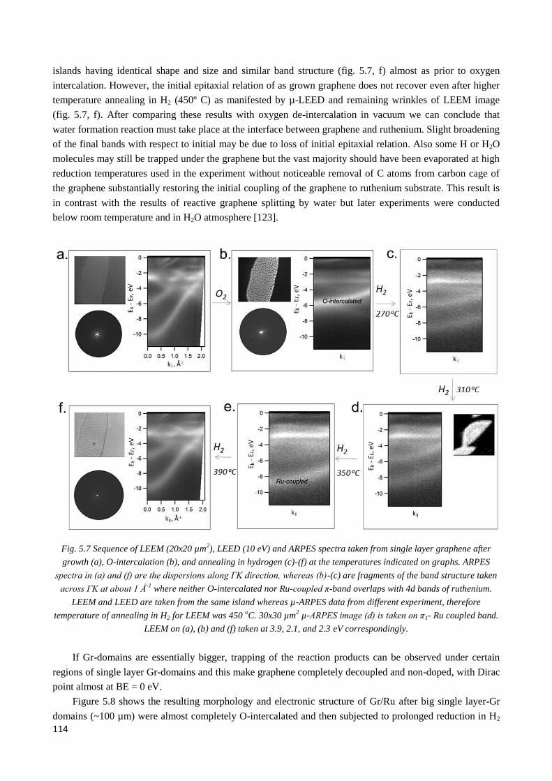
114
islands having identical shape and size and similar band structure (fig. 5.7, f) almost as prior to oxygen
intercalation. However, the initial epitaxial relation of as grown graphene does not recover even after higher
temperature annealing in H2 (450º C) as manifested by µ-LEED and remaining wrinkles of LEEM image
(fig. 5.7, f). After comparing these results with oxygen de-intercalation in vacuum we can conclude that
water formation reaction must take place at the interface between graphene and ruthenium. Slight broadening
of the final bands with respect to initial may be due to loss of initial epitaxial relation. Also some H or H2O
molecules may still be trapped under the graphene but the vast majority should have been evaporated at high
reduction temperatures used in the experiment without noticeable removal of C atoms from carbon cage of
the graphene substantially restoring the initial coupling of the graphene to ruthenium substrate. This result is
in contrast with the results of reactive graphene splitting by water but later experiments were conducted
below room temperature and in H2O atmosphere [123].
Fig. 5.7 Sequence of LEEM (20x20 µm
2), LEED (10 eV) and ARPES spectra taken from single layer graphene after
growth (a), O-intercalation (b), and annealing in hydrogen (c)-(f) at the temperatures indicated on graphs. ARPES
spectra in (a) and (f) are the dispersions along ΓK direction, whereas (b)-(c) are fragments of the band structure taken
across ΓK at about 1 Å-1
where neither O-intercalated nor Ru-coupled π-band overlaps with 4d bands of ruthenium.
LEEM and LEED are taken from the same island whereas µ-ARPES data from different experiment, therefore
temperature of annealing in H2 for LEEM was 450 oC. 30x30 µm
2 µ-ARPES image (d) is taken on π1- Ru coupled band.
LEEM on (a), (b) and (f) taken at 3.9, 2.1, and 2.3 eV correspondingly.
If Gr-domains are essentially bigger, trapping of the reaction products can be observed under certain
regions of single layer Gr-domains and this make graphene completely decoupled and non-doped, with Dirac
point almost at BE = 0 eV.
Figure 5.8 shows the resulting morphology and electronic structure of Gr/Ru after big single layer-Gr
domains (~100 µm) were almost completely O-intercalated and then subjected to prolonged reduction in H2
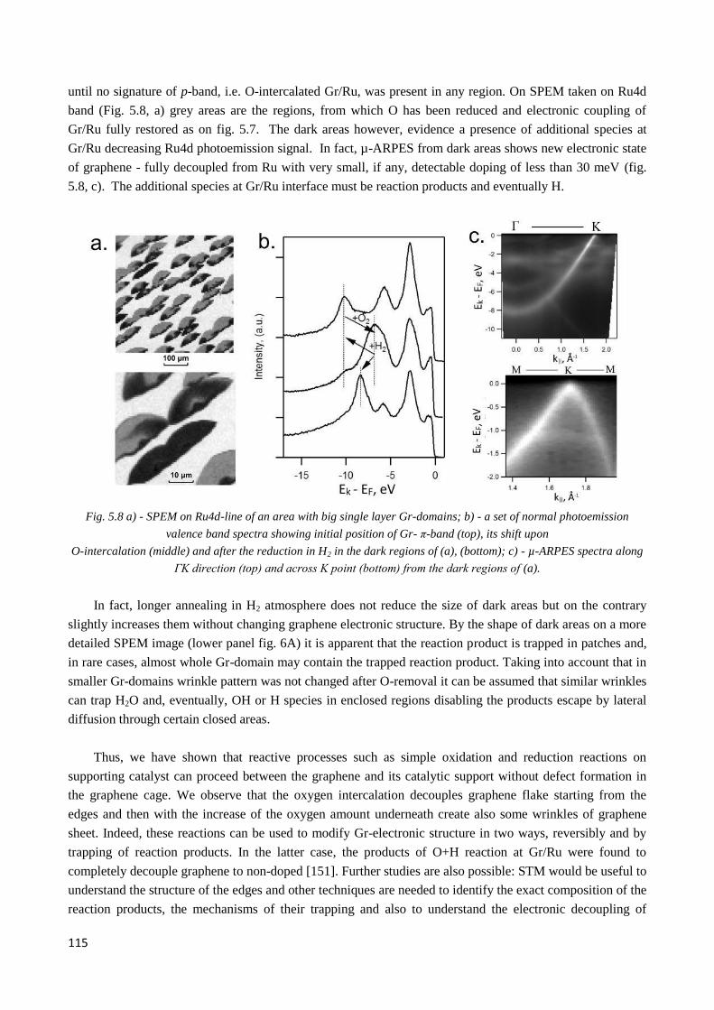
115
until no signature of p-band, i.e. O-intercalated Gr/Ru, was present in any region. On SPEM taken on Ru4d
band (Fig. 5.8, a) grey areas are the regions, from which O has been reduced and electronic coupling of
Gr/Ru fully restored as on fig. 5.7. The dark areas however, evidence a presence of additional species at
Gr/Ru decreasing Ru4d photoemission signal. In fact, µ-ARPES from dark areas shows new electronic state
of graphene - fully decoupled from Ru with very small, if any, detectable doping of less than 30 meV (fig.
5.8, c). The additional species at Gr/Ru interface must be reaction products and eventually H.
Fig. 5.8 a) - SPEM on Ru4d-line of an area with big single layer Gr-domains; b) - a set of normal photoemission
valence band spectra showing initial position of Gr- π-band (top), its shift upon
O-intercalation (middle) and after the reduction in H2 in the dark regions of (a), (bottom); c) - µ-ARPES spectra along
ΓK direction (top) and across K point (bottom) from the dark regions of (a).
In fact, longer annealing in H2 atmosphere does not reduce the size of dark areas but on the contrary
slightly increases them without changing graphene electronic structure. By the shape of dark areas on a more
detailed SPEM image (lower panel fig. 6A) it is apparent that the reaction product is trapped in patches and,
in rare cases, almost whole Gr-domain may contain the trapped reaction product. Taking into account that in
smaller Gr-domains wrinkle pattern was not changed after O-removal it can be assumed that similar wrinkles
can trap H2O and, eventually, OH or H species in enclosed regions disabling the products escape by lateral
diffusion through certain closed areas.
Thus, we have shown that reactive processes such as simple oxidation and reduction reactions on
supporting catalyst can proceed between the graphene and its catalytic support without defect formation in
the graphene cage. We observe that the oxygen intercalation decouples graphene flake starting from the
edges and then with the increase of the oxygen amount underneath create also some wrinkles of graphene
sheet. Indeed, these reactions can be used to modify Gr-electronic structure in two ways, reversibly and by
trapping of reaction products. In the latter case, the products of O+H reaction at Gr/Ru were found to
completely decouple graphene to non-doped [151]. Further studies are also possible: STM would be useful to
understand the structure of the edges and other techniques are needed to identify the exact composition of the
reaction products, the mechanisms of their trapping and also to understand the electronic decoupling of
116
graphene above the trapped reaction products. In case of inhomogeneity in graphene domains, such as the
presence of bilayer islands, lateral p-n junctions can be formed within the top layer of graphene upon oxygen
intercalation with dramatic chemical potential difference reaching 1.2 eV. Such big potential differences
cannot be reached by electrostatic gating because of insulator breakdown and can be used in production of
atomically thin devices which are interesting for photodetection [158] and also can be used as quantum dots
confining exotic massless Dirac fermion charge carriers within small-sized n-type doped Gr-patches [159,
160].
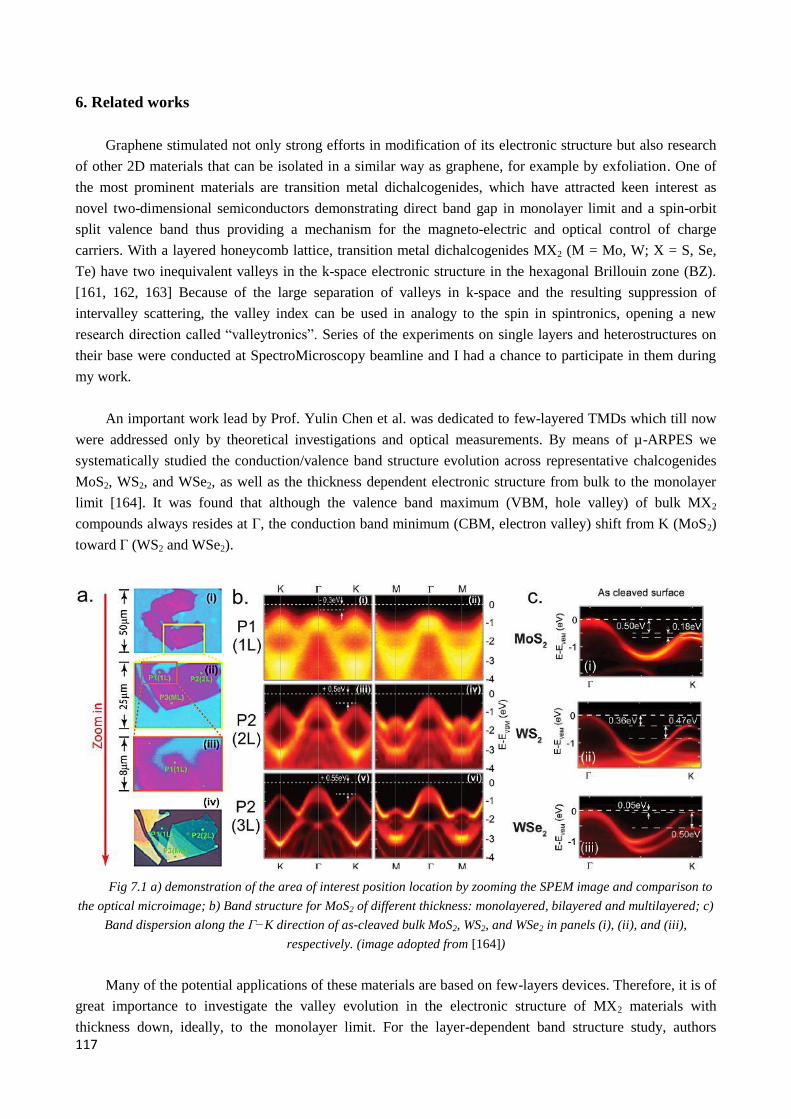
117
6. Related works
Graphene stimulated not only strong efforts in modification of its electronic structure but also research
of other 2D materials that can be isolated in a similar way as graphene, for example by exfoliation. One of
the most prominent materials are transition metal dichalcogenides, which have attracted keen interest as
novel two-dimensional semiconductors demonstrating direct band gap in monolayer limit and a spin-orbit
split valence band thus providing a mechanism for the magneto-electric and optical control of charge
carriers. With a layered honeycomb lattice, transition metal dichalcogenides MX2 (M = Mo, W; X = S, Se,
Te) have two inequivalent valleys in the k-space electronic structure in the hexagonal Brillouin zone (BZ).
[161, 162, 163] Because of the large separation of valleys in k-space and the resulting suppression of
intervalley scattering, the valley index can be used in analogy to the spin in spintronics, opening a new
research direction called “valleytronics”. Series of the experiments on single layers and heterostructures on
their base were conducted at SpectroMicroscopy beamline and I had a chance to participate in them during
my work.
An important work lead by Prof. Yulin Chen et al. was dedicated to few-layered TMDs which till now
were addressed only by theoretical investigations and optical measurements. By means of µ-ARPES we
systematically studied the conduction/valence band structure evolution across representative chalcogenides
MoS2, WS2, and WSe2, as well as the thickness dependent electronic structure from bulk to the monolayer
limit [164]. It was found that although the valence band maximum (VBM, hole valley) of bulk MX2
compounds always resides at Γ, the conduction band minimum (CBM, electron valley) shift from K (MoS2)
toward Γ (WS2 and WSe2).
Fig 7.1 a) demonstration of the area of interest position location by zooming the SPEM image and comparison to
the optical microimage; b) Band structure for MoS2 of different thickness: monolayered, bilayered and multilayered; c)
Band dispersion along the Γ−K direction of as-cleaved bulk MoS2, WS2, and WSe2 in panels (i), (ii), and (iii),
respectively. (image adopted from [164])
Many of the potential applications of these materials are based on few-layers devices. Therefore, it is of
great importance to investigate the valley evolution in the electronic structure of MX2 materials with
thickness down, ideally, to the monolayer limit. For the layer-dependent band structure study, authors
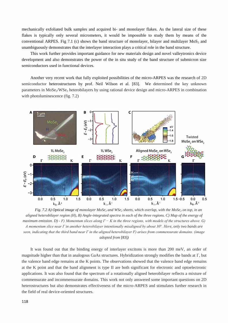
118
mechanically exfoliated bulk samples and acquired bi- and monolayer flakes. As the lateral size of these
flakes is typically only several micrometers, it would be impossible to study them by means of the
conventional ARPES. Fig 7.1 (c) shows the band structure of monolayer, bilayer and multilayer MoS2 and
unambiguously demonstrates that the interlayer interaction plays a critical role in the band structure.
This work further provides important guidance for new materials design and novel valleytronics device
development and also demonstrates the power of the in situ study of the band structure of submicron size
semiconductors used in functional devices.
Another very recent work that fully exploited possibilities of the micro-ARPES was the research of 2D
semiconductor heterostructures by prof. Neil Wilson et al. [83]. We determined the key unknown
parameters in MoSe2/WSe2 heterobilayers by using rational device design and micro-ARPES in combination
with photoluminescence (fig. 7.2)
Fig. 7.2 A) Optical image of monolayer MoSe2 and WSe2 sheets, which overlap, with the MoSe2 on top, in an
aligned heterobilayer region (H), B) Angle-integrated spectra in each of the three regions. C) Map of the energy of
maximum emission. D) - F) Momentum slices along Γ − K in the three regions, with models of the structures above. G)
A momentum slice near Γ in another heterobilayer intentionally misaligned by about 30°. Here, only two bands are
seen, indicating that the third band near Γ in the aligned heterobilayer F) arises from commensurate domains. (image
adopted from [83])
It was found out that the binding energy of interlayer excitons is more than 200 meV, an order of
magnitude higher than that in analogous GaAs structures. Hybridization strongly modifies the bands at Γ, but
the valence band edge remains at the K points. The observations showed that the valence band edge remains
at the K point and that the band alignment is type II are both significant for electronic and optoelectronic
applications. It was also found that the spectrum of a rotationally aligned heterobilayer reflects a mixture of
commensurate and incommensurate domains. This work not only answered some important questions on 2D
heterostructures but also demonstrates effectiveness of the micro-ARPES and stimulates further research in
the field of real device-oriented structures.
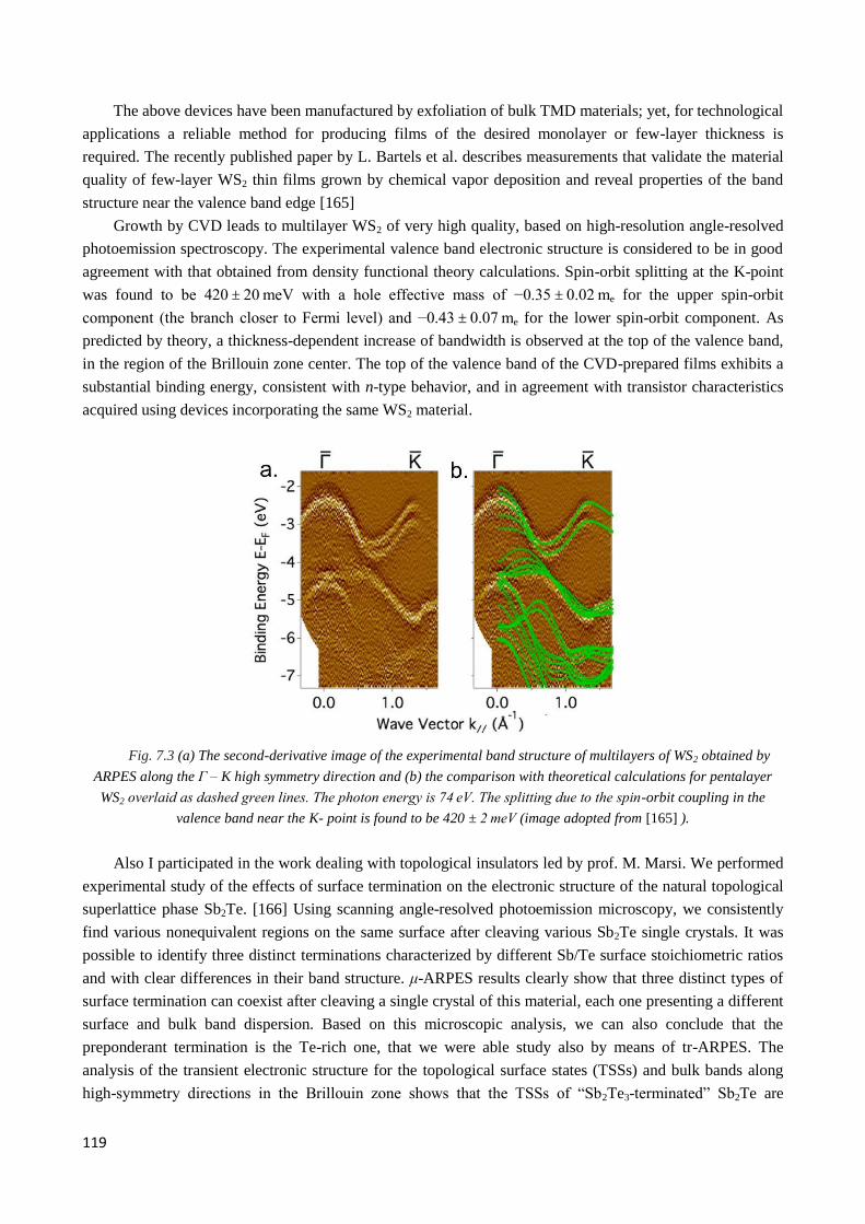
119
The above devices have been manufactured by exfoliation of bulk TMD materials; yet, for technological
applications a reliable method for producing films of the desired monolayer or few-layer thickness is
required. The recently published paper by L. Bartels et al. describes measurements that validate the material
quality of few-layer WS2 thin films grown by chemical vapor deposition and reveal properties of the band
structure near the valence band edge [165]
Growth by CVD leads to multilayer WS2 of very high quality, based on high-resolution angle-resolved
photoemission spectroscopy. The experimental valence band electronic structure is considered to be in good
agreement with that obtained from density functional theory calculations. Spin-orbit splitting at the K-point
was found to be 420 ± 20 meV with a hole effective mass of −0.35 ± 0.02 me for the upper spin-orbit
component (the branch closer to Fermi level) and −0.43 ± 0.07 me for the lower spin-orbit component. As
predicted by theory, a thickness-dependent increase of bandwidth is observed at the top of the valence band,
in the region of the Brillouin zone center. The top of the valence band of the CVD-prepared films exhibits a
substantial binding energy, consistent with n-type behavior, and in agreement with transistor characteristics
acquired using devices incorporating the same WS2 material.
Fig. 7.3 (a) The second-derivative image of the experimental band structure of multilayers of WS2 obtained by
ARPES along the Γ – K high symmetry direction and (b) the comparison with theoretical calculations for pentalayer
WS2 overlaid as dashed green lines. The photon energy is 74 eV. The splitting due to the spin-orbit coupling in the
valence band near the K- point is found to be 420 ± 2 meV (image adopted from [165] ).
Also I participated in the work dealing with topological insulators led by prof. M. Marsi. We performed
experimental study of the effects of surface termination on the electronic structure of the natural topological
superlattice phase Sb2Te. [166] Using scanning angle-resolved photoemission microscopy, we consistently
find various nonequivalent regions on the same surface after cleaving various Sb2Te single crystals. It was
possible to identify three distinct terminations characterized by different Sb/Te surface stoichiometric ratios
and with clear differences in their band structure. μ-ARPES results clearly show that three distinct types of
surface termination can coexist after cleaving a single crystal of this material, each one presenting a different
surface and bulk band dispersion. Based on this microscopic analysis, we can also conclude that the
preponderant termination is the Te-rich one, that we were able study also by means of tr-ARPES. The
analysis of the transient electronic structure for the topological surface states (TSSs) and bulk bands along
high-symmetry directions in the Brillouin zone shows that the TSSs of “Sb2Te3-terminated” Sb2Te are
120
considerably different from simple Sb2Te3, confirming that the surface properties of topological multilayers
are determined by more than one structural unit.
For the dominating Te-rich termination, authors also provide a direct observation of the excited
electronic states and of their relaxation dynamics by means of time-resolved angle-resolved photoemission
spectroscopy. These results clearly indicate that the surface electronic structure is strongly affected by the
bulk properties of the superlattice.
Our results discussed in Chapter 4 obtained on twisted graphene stimulated collaboration with Graphene
Instituted (Manchester, UK). Mr. Matthew Hammer produced differently misoriented bilayer graphene from
exfoliated graphene single layers manually controlling the twist angle. Measurements by us at
SpectroMicroscopy beamline clearly showed presence of interaction between layers that proves our results
obtained from nLG grown on SiC in situ. The high quality of the sample allowed us to observe multiple
supercell π-bands, which are predicted by theory for commensurate structures, twist-induced van Hove
singularities and correspondent band gaps. Such ARPES results for the bilayers with controllable angle of
rotation provide direct comparison with theoretical calculations, where certain angles allowing construction
of a finite supercell are used. Works on calculation of such system and analysis of the photoemission data are
now in progress and hopefully the results are coming soon.
121
7. Summary
The results of this work consist of two main parts: first one is dedicated to the investigation of electronic
properties of twisted multilayer graphene on SiC and their tuning by alkali metal intercalation and second
one sheds some light on the electronic properties of graphene on Ru(0001) and their changes tuning during
process of oxidation and reduction at Gr/Ru interface. We address the features of electronic structure using
micro-ARPES end-station at SpectroMicroscopy beamline at ELETTRA Synchrotron which allows
acquiring angle-resolved spectra from particularly small areas thanks to focused VUV beam (submicron
beam diameter).
In the beginning we synthesized multilayer graphene on SiC crystals by method of thermal
decomposition in both vacuum and argon ambient and on differently terminated planes (particularly, Si-
terminated and C-terminated). In the first case we found mostly monolayer or AB stacked bilayers that were
already well studied before. In the sample synthesized on C-face of SiC we found relatively big multilayer
graphene flakes with different number of graphene layers and different angle of rotation between them. We
acquired a big amount of data for differently stacked few-layer graphene and observed influence of the twist
angle on the interlayer coupling and Fermi velocity renormalization near K-point. For the big angles of
misorientation the graphene layers behave independently even in multilayer stacks, demonstrating linear
dispersion near K-point; however, for the small twist angles the situation is quite different as the interaction
between the layers increases. Our measurements confirmed the presence of van Hove singularities and
influence of the twist angle on their position as is was seen previously by STS. We found that charge carriers
in multilayer twisted graphene stack can propagate with different group velocities, which depend on the
mutual angle of rotation between the pair of layers. Thus, in trilayer graphene the middle layer will be
affected more by the layer which is rotated less. In case of extremely small angles of misorientation group
velocity can be non-zero in one direction and zero (e.g. flat band) in perpendicular one. Such locally flat
bands in the vicinity of the interacting π-bands were predicted by theoretical calculations and may give the
possibility for future simple realization of quasi-1D conductivity.
Further, we carried out intercalation of alkali metal atoms (Li and K) into the multilayer graphene stacks
intercalation and observed shift of the π-bands to lower kinetic energies (n-doping). After the atoms of
intercalant are allocated between the graphene sheets the distance between the latter gets bigger, but we still
observed the interlayer coupling but with corresponding formation of the VHSs. For case of intercalation of
the potassium atoms, which are comparatively huge we observed n-doping, which was expected and also the
preservation of the interlayer coupling. However, due to big size of the atoms, they become distributed non-
uniformly under the graphene layers which leads to observation of the π-bands with different doping from
the same certain spot. Thus, already for small number of layers (n ≥ 3) it makes the band structure quite
ambiguous and the tiny features are not easy to observe. Lithium atoms do not affect the system in such way
as they have smaller size and get distributed uniformly throughout the entire sample. So, after lithium doping
we could observe almost equal shifting of the π-bands graphene flake that allowed us to study selected
graphene stacks in details. Our measurements for the AA-stacked nLG confirmed the possibility of switching
to Bernal stack after some huge amount of intercalated Li atoms. In twisted graphene stacks we observed that
the interlayer coupling survives after intercalation and the amount of the intercalant can tune the position of
the van Hove singularities and local band gaps with respect to Fermi level. Another important achievement
is the creation of the direct band gap with width 0.08 ± 0.03 eV in the twisted 3LG.
Moreover, we observed the splitting of Dirac cone of the middle layer in case of doping of trilayer
graphene, similar to what was demonstrated by some theoretic works but not reported by spectroscopy
122
before. The π-band of the middle layer became split in two coaxial cones, which can be explained by the
influence of the electrostatic field from the intercalated atoms on the chirally behaving charge carriers in
graphene leading to Rashba-type pseudo-spin splitting or by overlap of the main and superlattice π-bands
having different doping and different Fermi velocities.
Second part of the work was dedicated to the synthesis of graphene on Ru(0001) using thermal cracking
of ethylene further oxygen intercalation/deintercalation and electronic structure changes studies during these
processes. It was observed that relatively high amount of ethylene in the chamber leads to the formation of
graphene layer on the surface and some excess of carbon atoms on it, that cause n-doping of graphene.
Formation of the carbon layer by segregation of the carbon from bulk to the surface during anneal creates
strongly coupled carbon layer that even shows no Dirac cones. The size of the domains can be controlled by
the amount of carbon dissolved in the bulk and can be varied in wide range: from submicron islands to full
coverage. Having grown tens of microns sized islands we studied the changes of the electronic structure of
graphene upon oxidation and reduction. After oxygen treatment graphene layer decouples starting from the
edge of the flake which is observed as change of the π-band from parabolic with massive charge carriers to
linearly dispersing with massless ones. If the bilayer patches are present within the domain after oxygen
intercalation they demonstrate p-doping while others are n-doped and lateral p-n junctions can be formed
with dramatic chemical potential difference reaching 1.2 eV. Hydrogen treatment removes oxygen and may
switch the system into its initial position in non-destructing way, however, in the relatively big domains we
observed still decoupled and non-doped graphene that is connected to the products of reaction that remain
trapped underneath due to presence of structural wrinkles after oxygen intercalation.
123
List of abbreviations
µ-ARPES microprobe angle-resolved photoemission spectroscopy
AFM atomic force microscopy
ARPES angle-resolved photoemission spectroscopy
BLG bilayer graphene
BZ Brillouin zone
CB conduction band
CBM conduction band minimum
CCD charge-coupled device
CDW charge density waves
CNP charge neutral points
CVD chemical vapor deposition
DFT density functional theory
DOS density of states
ED energy of Dirac point
EF Fermi energy
FWHM full width at half maximum
FZP Fresnel zone plate
HARPES hard X-ray angle-resolved photoemission spectroscopy
HFM horizontal focusing mirror
HR-ARPES high resolution angle resolved photoemission spectroscopy
HRM horizontal refocusing mirror
ID insertion device
IPES inverse photoemission spectroscopy
LDA+DMFT local density approximation + dynamical mean-field theory calculations
LEED low-energy electron diffraction
LEEM low-energy electron microscopy
Li-GIC Li-graphite intercalation compounds
MB superlattice Brillouin zone boundary, minizone boundary
mBZ mini Brillouin zone
MCP multi-channel plate
MIT metal-to-insulator transition
ML monolayer
NA numerical aperture
nLG few layer graphene
PE pass energy
PEEM photoemission electron microscopy
PI paramagnetic insulator
PM paramagnetic metal
PM plane mirror
RF radio frequency
SG spherical grating
SLG single layer graphene

124
SO Schwarzschild objective
SPEM scanning photoelectron microscopy
STM scanning tunneling microscopy
STS scanning tunneling spectroscopy
TB tight binding
TI topological insulator
TSSs topological surface states
TMDs transition metal dichalcogenides
UHV ultra-high vacuum
UPS ultraviolet photoelectron spectroscopy
UV ultraviolet
VB valence band
VBM valence band maximum
VFM vertical focusing mirror
VHS van Hove singularity
VRM vertical refocusing mirror
VUV vacuum ultraviolet
XPS X-ray photoelectron spectroscopy
μ-LEED microprobe low-energy electron diffraction

125
Acknowledgements
I would like to thank all the people, with whom I worked during my “PhD years”, and who made this
thesis possible to appear. First of I acknowledge my supervisor Dr. Alexei Barinov, who took me to
Spectromicroscopy team, gave me tons of new information about ARPES and many other subjects, inspired
me with constant upgrading of the beamline, and pushed me forward in creation of this work. I thank
Michael Yablonskih, Abdulla Al-Mahboob, Santosh Balijepalli and Alessio Giampietri, who worked at the
beamline during these years, spent many hours for preparation of the samples and acquisition of the data
presented here, and also shared shifts during beamtimes.
I acknowledge Prof. Naurang Saini, Prof. Marino Marsi, Prof. Ludwig Bartels, Prof. Yulin Chen and
their groups for interesting experiments in which I had chance to participate. Special thanks to Prof. Neil
Wilson and his team for long lasting fruitful collaboration. Your experiments always were something
awesome!
Thanks to Eugenio Nicolini for quick and high quality technical support for the laboratory. This always
allowed us thinking more about science than about technical problems.
Many thanks to my co-supervisor Prof. Fulvio Parmigiani for significant comments and thus serious
improvement of the thesis and also for interesting lectures on spectroscopy of solids
I would like to thank many people from ELETTRA Synchrotron, especially to Dr. Luca Gregoratti, Dr.
Andrea Lausi and people from HR Department. Thanks to all people from Doctorate Office at Physics
Department, without you this doctorate study would not be possible.
Also I want to thank my family, especially my dear wife Anya who waited for me in Ukraine during
these long years of my studies and gave me courage to work here in Italy
126
List of publications
Spectroscopic characterization of charge carrier anisotropic motion in twisted few-layer graphene, Kandyba V.,
Yablonskikh M., Barinov A., Scientific Reports, Vol. 5, pp. 16388 (2015)
Band structure characterization of WS2 grown by chemical vapor deposition, Tanabe I., Gomez M., Coley W., Le
D., Echeverria E., Stecklein G., Kandyba V., Balijepalli S., Klee V., Nguyen A., Preciado E., Lu I., Bobek S., Barroso
D., Martinez-Ta D., Barinov A., Rahman T., Dowben P., Crowell P., Bartels L., Applied Physics Letters, Vol. 108 - N,
pp. 252103 (2016)
Evolution of the Valley Position in Bulk Transition-Metal Chalcogenides and Their Monolayer Limit, Yuan H,
Liu Z, Xu G, Zhou B, Wu S, Dumcenco D, Yan K, Zhang Y, Mo S, Dudin P, Kandyba V, Yablonskikh M, Barinov A,
Shen Z, Zhang S, Huang Y, Xu X, Hussain Z, Hwang HY, Cui Y, Chen Y
Nano Lett. , 16 (8), pp 4738–4745 (2016)
Electronic structure of self-doped layered Eu3F4Bi2S4 material revealed by x-ray absorption spectroscopy and
photoelectron spectromicroscopy,
Paris E., Sugimoto T., Wakita T., Barinov A., Terashima K., Kandyba V., Proux O., Kajitani J., Higashinaka R.,
Matsuda T. D., Aoki Y., Yokoya T., Mizokawa T., Saini N. L., Physical Review B, Vol. 95 - 3, pp. 035152 (2017)
Electronic band structure for occupied and unoccupied states of the natural topological superlattice phase Sb2Te,
Khalil L., Papalazarou E., Caputo M., Nilforoushan N., Perfetti L., Taleb-Ibrahimi A., Kandyba V., Barinov A., Gibson
Q. D., Cava R. J., Marsi M., Physical Review B, Vol. 95 - 8, pp. 085118 (2017)
Determination of band offsets, hybridization, and exciton binding in 2D semiconductor heterostructures,Wilson
Neil R., Nguyen Paul V., Seyler Kyle, Rivera Pasqual, Marsden Alexander J., Laker Zachary P.L., Constantinescu
Gabriel C., Kandyba Viktor, Barinov Alexei, Hine Nicholas D.M., Xu Xiaodong, Cobden David H., Sci Adv, Vol. 3 - 2
(2017)
Single crystalline electronic structure and growth mechanism of aligned square graphene sheets, Yang H. F.,
Chen C., Wang H., Liu Z. K., Zhang T., Peng H., Schröter N. B. M., Ekahana S. A., Jiang J., Yang L. X., Kandyba V.,
Barinov A., Chen C. Y., Avila J., Asensio M. C., Peng H. L., Liu Z. F., Chen Y. L., APL Materials 6, 036107 (2018)
Tuning electronic properties by oxidation-reduction reactions at graphene-ruthenium interface, Viktor Kandyba;
Abdullah Al-Mahboob; Alessio Giampietri; Jerzy T Sadowski; Alexei Barinov, Carbon, Vol 138, pp. 271-276 (2018)
Results included in the thesis were presented at:
“International Winterschool on Electronic Properties of Novel Materials”, Kirchberg in Tirol, Austria, 03/2017 -
poster presentation
“52nd
Zakopane School of Physics Breaking Frontiers: Submicron Structures in Physics and Biology”, Zakopane,
Poland, May, 2017 - oral presentation
“FisMat 2017”, Miramare, Trieste, Italy, October, 2017 - oral presentation
127
Works Cited
[1] A. Damascelli, Z. Hussain and Z.-X. Shen, Rev. Mod. Phys., vol. 75, p. 473, 2003.
[2] W. Schattke and M. A. van Hove, Solid-State Photoemission and Related Methods. Theory and
Experiment, Weinheim: Wiley-VCH, 2003.
[3] D. W. Lynch and C. G. Olson, ‘Photoemission Studies of High-Temperature Superconductors,
Cambridge: Cambridge University Press, 1999.
[4] P. Puschnig and D. Lüftner, "Simulation of angle-resolved photoemission spectra by approximating
the final state by a plane wave: From graphene to polycyclic aromatic hydrocarbon molecules,"
Journal of Electron Spectroscopy and Related Phenomena, vol. 200, pp. 193-208, 2015.
[5] H. Ding, T. Yokoya, J. C. Campuzano and T. Takahashi, "Spectroscopic evidence for a pseudogap in the
normal state of underdoped high-Tc superconductors," Nature, vol. 382.6586, pp. 51-54, 1996.
[6] M. R. Norman, "Destruction of the Fermi surface in underdoped high-Tc superconductors," Nature,
vol. 392, pp. 157-160, 1998.
[7] A. Arko, J. Joyce, A. Andrews, J. Thompson, J. Smith, E. Moshopoulou, Z. Fisk, A. Menovsky, P. Canfield
and C. Olson, "Electronic structure of heavy fermions: Narrow temperature-independent bands,"
Physica B: Condensed Matter, vol. 230, pp. 16-21, 1997.
[8] H. J. Im, T. Ito, H.-D. Kim, S. Kimura, K. E. Lee, J. B. Hong, Y. S. Kwon, A. Yasui and H. H. Yamagami,
"Direct Observation of Dispersive Kondo Resonance Peaks in a Heavy-Fermion System," Phys. Rev.
Lett., vol. 100, p. 176402, 2008.
[9] C. Preinesberger, G. Pruskil, S. K. Becker and M. Dähne, "Structure and electronic properties of
dysprosium-silicide nanowires on vicinal Si(001)," Appl. Phys. Lett., vol. 87, p. 083107, 2005.
[10] Y. L. Chen, J. G. Analytis, J.-H. Chu, Z. K. Liu, S.-K. Mo, X. L. Qi, H. J. Zhang, D. H. Lu, X. Dai, Z. Fang, S. C.
Zhang, I. R. Fisher, Z. Hussain and Z.-X. Shen, "Experimental Realization of a Three-Dimensional
Topological Insulator, Bi2Te3," Science, vol. 10, no. 5937, pp. 178-181, 2009.
[11] D. Hsieh, Y. Xia, D. Qian, L. Wray, F. Meier, J. H. Dil, J. Osterwalder, L. Patthey, A. V. Fedorov, H. Lin, A.
Bansil, D. Grauer, Y. S. Hor, R. J. Cava and M. Z. Hasan, "Observation of Time-Reversal-Protected
Single-Dirac-Cone Topological-Insulator States in Bi2Te3 and Sb2Te3," Phys. Rev. Lett., vol. 103, no.
146401, 2009.
[12] L. X. Yang, Z. K. Liu, Y. Sun, H. Peng, H. F. Yang, T. Zhang, B. Zhou, Y. Zhang, Y. F. Guo, M. Rahn, D.
Prabhakaran, Z. Hussain, S.-K. Mo, C. Felser, B. Yan and Y. L. Chen, "Weyl semimetal phase in the non-
centrosymmetric compound TaAs," Nature Physics, vol. 11, p. 728–732, 2005.
[13] A. Einstein, Ann. Phys., vol. 31, p. 132, 1905.
128
[14] S. Hüfner, Photoelectron Spectroscopy, Berlin: Springer-Verlag, 1995.
[15] G. Lapeyre, R. Smith, J. Knapp and J. Anderson, "Constant final energy and constant initial energy
spectroscopy," Journal de Physique Colloques, vol. 39, no. C4, pp. C4-134-C4-141, 1978.
[16] W. L. David and G. O. Clifford, Photoemission Studies of High-Temperature Superconductors,
Cambridge: Cambridge University Press , 1999.
[17] "Electron Spectrometer Scienta R4000," VG Scienta, March 28 2010. [Online]. Available:
http://vgscienta.com/.
[18] J. Schwinger, "On the Classical Radiation of Accelerated Electrons," Phys. Rev., vol. 75, no. 1912, 1949.
[19] K.-J. Kim, Characteristics of synchrotron radiation. In X-ray data booklet., Center for X-ray optics and
advanced light source, 2001.
[20] C. Smallwood, J. Hinton, J. C., W. Zhang, J. Koralek, H. Eisaki, D.-H. Lee, J. Orenstein and A. Lanzara,
"Tracking Cooper Pairs in a Cuprate Superconductor by Ultrafast Angle-Resolved Photoemission,"
Science, vol. 336, no. 1137, 2012 .
[21] J. Graf, C. Jozwiak, C. L. Smallwood, H. Eisaki, R. A. Kaindl, D.-H. Lee and A. Lanzara, "Nodal
quasiparticle meltdown in ultrahigh-resolution pump-probe angle-resolved photoemission," Nature
Physics, vol. 7, pp. 805-809, 2011.
[22] J. A. Sobota, S. Yang, J. G. Analytis, Y. L. Chen, I. R. Fisher, P. S. Kirchmann and Z.-X. Shen, "Ultrafast
Optical Excitation of a Persistent Surface-State Population in the Topological Insulator Bi2Se3," Phys.
Rev. Lett., vol. 108, no. 117403, p. 2012.
[23] F. Schmitt, P. Kirchmann, U. Bovensiepen, R. Moore, G.-H. Chu, D. Lu, L. Rettig, M. Wolf, I. Fisher and
Z.-X. Shen, "Ultrafast electron dynamics in the charge density wave material TbTe3," New Journal of
Physics, vol. 13, 2011.
[24] S. Ulstrup, J. C. Johannsen, F. Cilento, J. A. Miwa, A. Crepaldi, M. Zacchigna, C. Cacho, R. Chapman, E.
Springate, S. Mammadov, F. Fromm, C. Raidel, T. Seyller, F. Parmigiani, M. Grioni, P. King and P.
Hofmann, "Ultrafast Dynamics of Massive Dirac Fermions in Bilayer Graphene," Phys. Rev. Lett., vol.
112, p. 257401, 2014.
[25] J. C. Johannsen, S. Ulstrup, A. Crepaldi, F. Cilento, M. Zacchigna, J. A. Miwa, C. Cacho, R. T. Chapman,
E. Springate, F. Fromm, C. Raidel, T. Seyller, P. King, F. Parmigiani, M. Grioni and P. Hofmann,
"Tunable Carrier Multiplication and Cooling in Graphene," Nano Lett., vol. 15, no. 1, pp. 326-331,
2014.
[26] M. Hoesch, T. Greber, V. Petrov, M. Muntwiler, M. Hengsberger, W. Auwarter and J. Osterwalde,
"Spin-polarized Fermi surface mapping," Journal of Electron Spectroscopy and Related Phenomena,
vol. 124, p. 263–279, 2002.
[27] A. X. Gray, C. Papp, S. Ueda, B. Balke, Y. Yamashita, L. Plucinski, J. Minár, J. Braun, E. R. Ylvisaker, C. M.
129
Schneider, W. E. Pickett, H. Ebert, K. Kobayashi and C. S. Fadley, "Probing bulk electronic structure
with hard X-ray angle-resolved photoemission," Nature Materials, vol. 10, p. 759–764, 2011.
[28] L. Plucinski, J. Minár, B. C. Sell, J. Braun, H. Ebert, C. M. Schneider and C. S. Fadley, "Band mapping in
higher-energy x-ray photoemission: Phonon effects and comparison to one-step theory," Phys. Rev. B
78, 035108 (2008)., vol. 78, no. 035108, 2008.
[29] K. Kobayashi, "High-resolution hard X-ray photoelectron spectroscopy: Application of valence band
and core-level spectroscopy to materials science," Nucl. Instrum. Methods Phys. Res. A, vol. 547, no.
1, pp. 98-112, 2005.
[30] A. Septier, "Geometrical Electron Optics," in Electron Microscopy in Material Science, Academic Press,
1971, pp. 15-73.
[31] T. Menteş, G. Zamborlini, A. Sala and A. Locatelli, "Cathode lens spectromicroscopy: methodology and
applications," Beilstein J Nanotechnol., vol. 5, p. 1873–1886, 2014.
[32] D. L. Shealy, C. Wang and R. B. Hoover, "Optical analysis of an ultra-high resolution two-mirror soft x-
ray microscope," J. X-Ray Sci. Technol., vol. 5(1), pp. 1-19, 1995.
[33] R. B. Hoover, D. L. Shealy, B. R. Brinkley, P. C. Baker, J. Troy W. Barbee and A. B. C. Walker,
"Development of the water window imaging x-ray microscope utilizing normal incidence multilayer
optics," Opt. Eng., vol. 30(8), pp. 1086-1093, 1991.
[34] D. L. Shealy, W. Jiang and R. Hoover, "Design and analysis of aspherical multilayer imaging x-ray," Opt.
Eng., vol. 30(8), p. 1094, 1991.
[35] A. I. and K. K., "Schwarzschild objective for soft x-rays," Opt. Eng., vol. 39(8), pp. 2163-2170, 2000.
[36] F. Barbo, M. Bertolo, A. Bianco, G. Cautero, S. Fontana, T. K. Johal, S. La Rosa and G. Margaritondo,
"Spectromicroscopy beamline at ELETTRA: Performances achieved at the end of commisioning," Rev.
Sci. Instrum., vol. 71, no. 5, 2000.
[37] W. Chao, J. Kim, S. Rekawa, P. Fischer and E. Anderson, "Demonstration of 12 nm Resolution Fresnel
Zone Plate Lens based Soft X-ray Microscopy," Optics Express, vol. 17, no. 20, pp. 17669-17677, 2009.
[38] B. Diviacco, R. Bracco, C. Poloni, R. P. Walker and D. Zangrando, Rev. Sci. Instrum., vol. 63, p. 388–391,
1992.
[39] P. Dudin, P. Lacovig, C. Fava, E. Nicolini, A. Bianco, G. Cautero and A. Barinov, "Angle-resolved
photoemission spectroscopy and imaging with a submicrometre probe at the SPECTROMICROSCOPY-
3.2L beamline of Elettra," J. Synchrotron Rad., vol. 17, pp. 445-450, 2010.
[40] L. Gregoratti, M. Marsi, G. Cautero, M. Kiskinova, G. R. Morrison and A. W. Potts, "Spectromicroscopy
of interfaces with synchrotron radiation: multichannel data acquisition," Nucl. Instrum. Methods
Phys. Res. A, vol. 467–468 , pp. 884-888, 2001.
130
[41] A. Oelsner, O. Schmidt, M. Schicketanz, M. Klais, G. Schönhense, V. Mergel, O. Jagutzki and H.
Schmidt-Bocking, "Microspectroscopy and imaging using a delay line detector in time-of-flight
photoemission microscopy," Review of Scientific Instruments, vol. 72, no. 10, pp. 3968 - 3974, 2001.
[42] S. C. Speller, P. Dudin, S. Fitzgerald, G. M. Hughes, K. Kruska, T. B. Britton, A. Krzton-Maziopa, E.
Pomjakushina, K. Conder, A. Barinov and C. R. M. Grovenor, "High-resolution characterization of
microstructural evolution in RbxFe2−ySe2 crystals on annealing," Phys. Rev. B, vol. 90, pp. 024520-1 -
024520-8, 2014.
[43] S. Lupi, L. Baldassarre, B. Mansart, A. Perucchi, A. Barinov, P. Dudin, E. Papalazarou, F. Rodolakis, J.-P.
Rueff, J.-P. Itié, S. Ravy, D. Nicoletti, P. Postorino, P. Hansmann, N. Parragh, A. Toschi, T. Saha-
Dasgupta and O. K. e. a. Andersen, "A microscopic view on the Mott transition in chromium-doped
V2O3," Nat. Comm., vol. 1, p. 105, 2010.
[44] L. Bignardi, W. van Dorp, S. Gottardi, O. Ivashenko, P. Dudin, A. Barinov, J. T. M. De Hosson, M. Stöhr
and P. Rudolf, "Microscopic characterisation of suspended graphene grown by chemical vapour
deposition," Nanoscale, vol. 5, pp. 9057-9061, 2013.
[45] D. Le, A. Barinov, E. Preciado, M. Isarraraz, I. Tanabe, T. Komesu, C. Troha, L. Bartels, T. Rahman and
P. Dowben, "Spin–orbit coupling in the band structure of monolayer WSe2," J. Phys.: Condens.
Matter, vol. 27, p. 182201, 2015.
[46] P.-C. Yeh, W. Jin, N. Zaki, D. Zhang, J. Liou, J. Sadowski, A. Al-Mahboob, J. Dadap, I. Herman, P. Sutter
and J. R. Osgood, "Layer-dependent electronic structure of an atomically heavy two-dimensional
dichalcogenide," Phys. Rev. B, vol. 91, pp. 041407-1 - 041407-6, 2015.
[47] "Endstation Tables - maestro," 2017. [Online]. Available:
https://sites.google.com/a/lbl.gov/maestro/instrumentation/endstation-tables. [Accessed 2017].
[48] A. Bostwick, E. i Rotenberg, J. Avila and M. Asensio, "Zooming in on Electronic Structure: NanoARPES
at SOLEIL and ALS," Synchrotron radiation news, vol. 25, no. 5, pp. 19-25, 2012.
[49] "I05 - Surfaces and Interfaces - Diamond Light Source," 2017. [Online]. Available:
http://www.diamond.ac.uk/Beamlines/Surfaces-and-Interfaces/I05.html. [Accessed 2017].
[50] K. S. Novoselov, A. K. Geim, S. V. Morozov, D. Jiang, Y. Zhang, S. V. Dubonos, I. V. Grigorieva and A. A.
Firsov, "Electric Field Effect in Atomically Thin Carbon Films," Science, vol. 306, 2004.
[51] D. Cooper, B. D’Anjou, N. Ghattamaneni, B. Harack, M. Hilke, A. Horth, N. Majlis, M. Massicotte, L.
Vandsburger, E. Whiteway and V. Yu, "Experimental Review of Graphene," Condensed Matter Physics,
vol. 2012, 2012.
[52] D. V. Kosynkin, A. L. Higginbotham, A. Sinitskii, J. R. Lomeda, A. Dimiev, B. K. Price and J. M. Tour,
"Longitudinal unzipping of carbon nanotubes to form graphene nanoribbons," Nature, vol. 458, pp.
872-876, 2009.
131
[53] L. Jiao, L. Zhang, X. Wang, G. Diankov and H. Dai, "Narrow graphene nanoribbons from carbon
nanotubes," Nature, vol. 458, pp. 877-880, 2009.
[54] R. Balog, B. Jørgensen, L. Nilsson, M. Andersen, E. Rienks, M. Bianchi, M. Fanetti, E. Laegsgaard, A.
Baraldi, S. Lizzit, Z. Sljivancanin, F. Besenbacher, B. Hammer, T. Pedersen, P. Hofmann and L.
Hornekaer, "Bandgap opening in graphene induced by patterned hydrogen adsorption," Nat. Mater.,
vol. 9, no. 4, pp. 315-9, 2010.
[55] A. R. Muniz and D. Maroudas, "Superlattices of Fluorinated Interlayer-Bonded Domains in Twisted
Bilayer Graphene," J. Phys. Chem. C, vol. 117, no. 14, pp. 7315-7325, 2013.
[56] F. Ouyang, S. Peng, Z. Liu and Z. Liu, "Bandgap opening in graphene antidot lattices: the missing half,"
ACS Nano, vol. 5, no. 5, pp. 4023-30, 2011.
[57] J. H. Jørgensen, A. G. Čabo, R. Balog, L. Kyhl, M. N. Groves, A. M. Cassidy, A. Bruix, M. Bianchi, M.
Dendzik, M. A. Arman, L. Lammich, J. I. Pascual, J. Knudsen, B. Hammer, P. Hofmann and L.
Hornekaer, "Symmetry-Driven Band Gap Engineering in Hydrogen Functionalized Graphene," ACS
Nano, vol. 10, no. 12, p. 10798–10807, 2016.
[58] M. Y. Han, B. Özyilmaz, Y. Zhang and P. Kim, "Energy band-gap engineering of graphene
nanoribbons," Physical Review Letters, vol. 98, no. 20, 2007.
[59] P. Xu, M. Ackerman, S. Barber, J. Schoelz, P. Thibado, V. Wheeler, L. Nyakiti, R. Myers-Ward, J. C. Eddy
and D. Gaskill, "Competing scanning tunneling microscope tip-interlayer interactions for twisted
multilayer graphene on the a-plane SiC surface," Surface Science, vol. 617, pp. 113-117, 2013.
[60] K. I. Bolotin, K. J. Sikes, Z. Jiang, M. Klima, G. Fudenberg, J. Hone, P. Kim and H. Stormer, "Ultrahigh
electron mobility in suspended graphene," Solid State Communications, vol. 146, no. 9-10, pp. 351-
355, 2008.
[61] J. C. Meyer, A. K. Geim, M. I. Katsnelson, K. S. Novoselov, T. J. Booth and S. Roth, "The structure of
suspended graphene sheets," Nature, vol. 446, pp. 60-63, 2007.
[62] A. Fasolino, J. H. Los and M. I. Katsnelson, "Intrinsic ripples in graphene," Nature Materials, vol. 6, no.
11, pp. 858-861, 2007.
[63] A. H. Castro Neto, F. Guinea, N. M. R. Peres, K. S. Novoselov and A. K. Geim, "The electronic
properties of graphene," Reviews of Modern Physics, vol. 81, pp. 110-155, 2009.
[64] P. R. Wallace, "The Band Theory of Graphite," Phys. Rev., vol. 71, no. 622, 1947.
[65] C.-H. Park, L. Yang, Y.-W. Son, M. L. Cohen and S. G. Louie, "Anisotropic behaviors of massless Dirac
fermions in graphene under periodic potentials," Nature Phys., vol. 4, pp. 213-217, 2008.
[66] D. Pesin and A. H. MacDonald, "Spintronics and pseudospintronics in graphene and topological
insulators," Nature Materials, vol. 11, pp. 409-416, 2012.
132
[67] L. Min, R. Hovden, P. Huang, M. Wojcik, D. A. Muller and J. Park, "Twinning and Twisting of Tri- and
Bilayer Graphene," Nano Letters, vol. 12, no. 3, pp. 1609-1615, 2002.
[68] E. Mostaani, N. D. Drummond and V. I. Fal'ko, "Quantum Monte Carlo Calculation of the Binding
Energy of Bilayer Graphene," Phys. Rev. Lett., vol. 115, no. 115501, 2015.
[69] T. Ohta, A. Bostwick, T. Seyller, K. Horn and E. Rotenberg, "Controlling the electronic structure of
bilayer graphene," Science, no. 313, pp. 951-954, 2006.
[70] Y. Zhang, T.-T. Tang, C. Girit, Z. Hao, M. C. Martin, A. Zettl, M. F. Crommie, Y. R. Shen and F. Wang,
"Direct Observation of a Widely Tunable Bandgap in Bilayer Graphene," Nature, vol. 459, pp. 820-823,
2009.
[71] P. Xu, M. L. Ackerman, S. D. Barber, J. K. Schoelz, P. M. Thibado, V. D. Wheeler, L. O. Nyakiti, R. L.
Myers-Ward, J. C. R. Eddy and D. K. Gaskill, "Competing scanning tunneling microscope tip-interlayer
interactions for twisted multilayer graphene on the a-plane SiC surface," Surface Science, vol. 617, pp.
113-117, 2013.
[72] J. Velasco Jr., L. Jing, W. Bao, Y. Lee, P. Kratz, V. Aji, M. Bockrath, C. N. Lau, C. Varma, R. Stillwell, D.
Smirnov, F. Zhang, J. Jung and A. H. MacDonald, "Transport spectroscopy of symmetry-broken
insulating states in bilayer graphene," Nat. Nanotechnol., vol. 7, p. 156, 2012.
[73] W. Yan, M. Liu, R.-F. Dou, L. Meng, L. Feng, Z.-D. Chu, Y. Zhang, Z. Liu, J.-C. Nie and L. He, "Angle-
Dependent van Hove Singularities in a Slightly Twisted Graphene Bilayer," Phys. Rev. Lett., vol. 109,
no. 126801, 2012.
[74] J. M. B. Lopes dos Santos, N. M. R. Peres and A. H. Castro Neto, "Graphene Bilayer with a Twist:
Electronic Structure," Phys. Rev. Lett., vol. 99, no. 256802, 2007.
[75] M. S. Dresselhaus and G. Dresselhaus, "Intercalation compounds of graphite," Adv. Phys., vol. 51, no.
1, pp. 1-186, 2002.
[76] F. Guinea, A. H. Castro Neto and N. M. R. Peres, "Electronic states and Landau levels in graphene
stacks," Phys. Rev., vol. 73, no. 245426, 2006.
[77] B. Partoens and F. M. Peeters, "From graphene to graphite: Electronic structure around the K point,"
Phys. Rev. B, vol. 74, no. 075404, 2006.
[78] L. Meng, R. Wu, L. Zhang, L. Li, S. Du, Y. Wang and H.-J. Gao, "Multi-oriented moiré superstructures of
graphene on Ir(111): experimental observations and theoretical models," Journal of Physics:
Condensed Matter, vol. 24, no. 31, 2012.
[79] J. Coraux, A. T. N'Diaye, M. Engler, C. Busse, D. Wall, N. Buckanie, F. J. Meyer zu Heringdorf, R. van
Gastel, B. Poelsema and T. Michely, "Growth of graphene on Ir(111)," New Journal of Physics, vol. 11,
no. 039801, 2009.
[80] A. Luican-Mayera, G. Li and A. E.Y., "Atomic scale characterization of mismatched graphene layers,"
133
Journal of Electron Spectroscopy and Related Phenomena, no. In Press, Corrected Proof, 2017.
[81] Z.-D. Chu, W.-Y. He and L. He, "Coexistence of van Hove singularities and superlattice Dirac points in a
slightly twisted graphene bilayer," Phys. Rev. B, vol. 87, no. 155419, 2013.
[82] D. Wong, Y. Wang, J. Jung, S. Pezzini, A. M. DaSilva, H.-Z. Tsai, H. S. Jung, R. Khajeh, Y. Kim, J. Lee, S.
Kahn, S. Tollabimazraehno, H. Rasool, K. Watanabe, T. Taniguchi, A. Zettl, S. Adam, A. H. MacDonald
and M. F. Crommie, "Local spectroscopy of moire-induced electronic structure ingate-tunable twisted
bilayer graphene," Phys. Rev. B., vol. 92, no. 155409, 2015.
[83] N. Wilson, P. Nguyen, K. Seyler, P. Rivera, A. Marsden, Z. Laker, G. Constantinescu, V. Kandyba, A.
Barinov, N. Hine, X. Xu and D. Cobden, "Determination of band offsets, hybridization, and exciton
binding in 2D semiconductor heterostructures," Sci. Adv., vol. 3, no. e1601832, 2017.
[84] M. R.S., "The Van Hove Singularity and High-Tc Superconductivity: The Role of (Nanoscopic)
Disorder," in High-Temperature Superconductivity, Boston, MA, Springer, 1991, pp. 555-560.
[85] L. Force and J. Bok, "Superconductivity in two dimensional systems: Van Hove singularity and
Coulomb repulsion," Solid State Communications, vol. 85, no. 11, pp. 975-978, 1993.
[86] J. L. McChesney, A. Bostwick, T. Ohta, T. Seyller, K. Horn, .. González and E. Rotenberg, "Extended van
Hove Singularity and Superconducting Instability in Doped Graphene," Phys. Rev. Lett., vol. 104, p.
136803, 2010.
[87] J. González, "Magnetic and Kohn-Luttinger instabilities near a Van Hove singularity: Monolayer versus
twisted bilayer graphene," Phys. Rev. B 88, vol. 88, p. 125434, 2013.
[88] Y. Cao, V. Fatemi, S. Fang, K. Watanabe, T. Taniguchi, E. Kaxiras and P. Jarillo-Herrero,
"Unconventional superconductivity in magic-angle graphene superlattices," Nature, vol. 556, pp. 43-
50, 2018.
[89] A. Luican, G. Li, A. Reina, J. Kong, R. R. Nair, K. S. Novoselov, A. K. Geim and E. Y. Andrei, "Single-Layer
Behavior and Its Breakdown in Twisted Graphene Layers," Phys. Rev. Lett., vol. 106, no. 126802, 2011.
[90] I. Brihuega, P. Mallet, H. Gonzalez-Herrero, G. Trambly de Laissardière, M. M. Ugeda, L. Magaud, J. M.
Gomez-Rodrıguez, F. Yndurain and J.-Y. Veuillen, "Unraveling the Intrinsic and Robust Nature of van
Hove Singularities in Twisted Bilayer Graphene by Scanning Tunneling Microscopy and Theoretical
Analysis," Phys. Rev. Lett., vol. 109, no. 196802, 2012.
[91] G. Trambly de Laissardiere, D. Mayou and L. Magaud, "Localization of Dirac electrons in rotated
graphene bilayers," Nano Lett., vol. 10, pp. 804-808, 2010.
[92] S. Latil, V. Meunier and L. Henrard, "Massless fermions in multilayer graphitic systems with
misoriented layers: Ab initio calculations and experimental fingerprints," Phys. Rev. B., vol. 76, no.
201402(R), 2007.
[93] E. Suarez Morell, J. D. Correa, P. Vargas, M. Pachecco and Z. Barticevic, "Flat bands in slightly twisted
134
bilayer graphene: tight binding calculations," Phys. Rev. B, vol. 82, no. 121140(R), 2010.
[94] L. Xian, Z. F. Wang and M. Y. Chou, "Coupled Dirac Fermions and Neutrino-like Oscillations in Twisted
Bilayer Graphene," Nano Lett., vol. 13, no. 11, pp. 5159-5164, 2013.
[95] R. Bistritzer and A. H. MacDonald, "Moire bands in twisted double-layer graphene," Proc. Natl. Acad.
Sci. USA 108, 12233–1237, (2011)., vol. 108, pp. 1233-1237, 2011.
[96] M. I. Katsnelson, K. S. Novoselov and A. K. Geim, "Chiral tunneling and Klein paradox in graphene,"
Nature Phys., vol. 2, pp. 620-625, 2006.
[97] A. Bostwick, T. Ohta, T. Seyller, K. Horn and E. Rotenberg, "Quasiparticle dynamics in graphene,"
Nature Physics, vol. 3, pp. 36-40, 2007.
[98] K. V. Emtsev, T. Seyller, F. Speck, L. Ley, P. Stojanov, J. D. Riley and R. C. G. Leckey, "Initial Stages of
the Graphite-SiC(0001) Interface Formation Studied by Photoelectron Spectroscopy," Materials
Science Forum, Vols. 556-557, pp. 525-528, 2007.
[99] I. Forbeaux, J. M. Themlin and J. M. Debever, "Heteroepitaxial graphite on 6H-SiC(0001): Interface
formation through conduction-band electronic structure," Phys. Rev. B, vol. 58, pp. 16396-16406,
1998.
[100] E. L. Shirley, L. J. Terminello, A. Santoni and F. J. Himpsel, "Brillouin-zone-selection effects in graphite
photoelectron angular distributions," Phys. Rev. B, vol. 51, p. 13614, 1995.
[101] I. Gierz, J. Henk, H. Hochst, C. R. Ast and K. Kern, "Illuminating the dark corridor in graphene:
Polarization dependence of angle-resolved photoemission spectroscopy on graphene," Phys. Rev. B,
vol. 83, p. 121408, 2011.
[102] M. Mucha-Kruczyński, O. Tsyplyatyev, A. Grishin, E. McCann, V. I. Fal’ko, A. Bostwick and E. Eli
Rotenberg, "Characterization of graphene through anisotropy of constant-energy maps in angle-
resolved photoemission," Phys. Rev. B, vol. 77, p. 195403, 2008.
[103] M. Sprinkle, D. Siegel, Y. Hu, J. Hicks, A. Tejeda, A. Taleb-Ibrahimi, P. Le Fèvre, F. Bertran, S. Vizzini, H.
Enriquez, S. Chiang, P. Soukiassian, C. Berger, W. A. de Heer, A. Lanzara and E. H. Conrad, "First Direct
Observation of a Nearly Ideal Graphene Band Structure," Phys. Rev. Lett., vol. 103, no. 226803, 2009.
[104] J. Hicks, M. Sprinkle, K. Shepperd and F. Wang, "Symmetry breaking in commensurate graphene
rotational stacking: Comparison of theory and experiment," Phys. Rev. B, vol. 83, no. 205403, 2011.
[105] T. Ohta, J. T. Robinson, P. J. Feibelman, A. Bostwick, E. Rotenberg and T. E. Beechem, "Evidence for
Interlayer Coupling and Moiré Periodic Potentials in Twisted Bilayer Graphene," Phys. Rev. Lett., vol.
109, no. 186807, 2012.
[106] A. Mugarza and J. E. Ortega, "Electronic states at vicinal surfaces," J. Phys. Condens. Matter 15, S3281
(2003)., vol. 15, p. S3281–S3310, 2003.
135
[107] S. Watcharinyanon, L. I. Johansson, A. A. Zakharov and C. Virojanadara, "Studies of Li intercalation of
hydrogenated graphene on SiC(0001)," Surface Science, Volume 606, Issues 3–4, 2012, Pages 401–
406, vol. 606, no. 3-4, pp. 401-406, 2012.
[108] S. Watcharinyanon, C. Virojanadara and L. I. Johansson, "Rb and Cs deposition on epitaxial graphene
grown on 6H-SiC(0001)," Surface Science, vol. 605, no. 21-22, pp. 1918-1922, 2011.
[109] F. Symalla, S. Shallcross, I. Beljakov, K. Fink, W. Wenzel and V. Meded, "Band-gap engineering with a
twist: Formation of intercalant superlattices in twisted graphene bilayers," Phys. Rev. B, vol. 91, no.
205412, 2015.
[110] S. Y. Zhou, G.-H. Gweon, J. Graf, A. V. Fedorov, C. D. Spataru1, R. D. Diehl, Y. Kopelevich, D.-H. Lee, S.
G. Louie and A. Lanzara, "First direct observation of Dirac fermions in graphite," Nature Physics, vol. 2,
no. 595-599, 2006.
[111] W. Norimatsu and M. M. Kusunoki, "Epitaxial graphene on SiC{0001}: advances and perspectives,"
Phys. Chem. Chem. Phys., vol. 16, no. 8, pp. 3501-3511, 2014.
[112] L. N. Srivastava, G. He and R. M. Feenstra, "Comparison of graphene formation on C-face and Si-face
SiC {0001} surfaces," Phys. Rev. B, vol. 82, no. 235406, 2010.
[113] P. Xu, D. Qi, J. K. Schoelz, J. Thompson, P. M. Thibado, V. D. Wheeler, L. Nyakiti, R. L. Myers-Ward, C.
R. Eddy Jr., D. K. Gaskill, M. Neek-Amal and F. M. Peeters, "Multilayer graphene, Moiré patterns, grain
boundaries and defects identified by scanning tunneling microscopy on the m-plane, non-polar
surface of SiC," Carbon, vol. 80, pp. 75-81, 2014.
[114] B. K. Daas, S. U. Omar, S. Shetu, K. M. Daniels, S. Ma, T. S. Sudarshan and M. V. S. Chandrashekhar,
"Comparison of Epitaxial Graphene Growth on Polar and Nonpolar 6H-SiC Faces: On the Growth of
Multilayer Films," Cryst. Growth Des., vol. 12, no. 7, pp. 3379-3387, 2012.
[115] P. W. Sutter, J.-. I. Flege and E. A. Sutter, "Epitaxial graphene on ruthenium," Nature Materials, vol. 7,
pp. 406-411, 2008.
[116] A. A. Rybkina, A. G. Rybkin, V. K. Adamchuk, D. Marchenko, A. Varykhalov, J. Sánchez-Barriga and A.
M. Shikin, "The graphene/Au/Ni interface and its application in the construction of a graphene spin
filter," Nanotechnology, Volume 24, Number 29 , vol. 24, no. 29, 2013.
[117] E. Voloshina and Y. Dedkov, "Graphene on metallic surfaces: problems and perspectives," Phys.
Chem. Chem. Phys., vol. 14, pp. 13502-13514, 2012.
[118] A. Varykhalov, J. Sánchez-Barriga, A. M. Shikin, C. Biswas, E. Vescovo, A. Rybkin, D. Marchenko and O.
Rader, "Electronic and Magnetic Properties of Quasifreestanding Graphene on Ni," Phys. Rev. Lett.,
vol. 101, no. 157601, 2008.
[119] C. Riedl, C. Coletti, T. Iwasaki, A. A. Zakharov and U. Starke, "Quasi-Free-Standing Epitaxial Graphene
on SiC Obtained by Hydrogen Intercalation," Phys. Rev. Lett., vol. 103, no. 246804, 2009.
136
[120] P. Sutter, J. T. Sadowski and E. A. Sutter, "Chemistry under Cover: Tuning Metal−Graphene Interaction
by Reactive Intercalation," J. Am. Chem. Soc., vol. 132, no. 23, pp. 8175-8179, 2010.
[121] R. Larciprete, S. Ulstrup, p. Lacovig, M. Dalmiglio, M. Bianchi, M. F. L. Hornekær, F. Orlando, A.
Baraldi, P. Hofmann and S. Lizzit, "Oxygen Switching of the Epitaxial Graphene–Metal Interaction,"
ACS Nano, vol. 6, no. 11, pp. 9551-9558, 2012.
[122] E. E. Wolf and F. Alfani, "Catalysts Deactivation by Coking," Catal. Sci. Eng., vol. 24, no. 3, pp. 329-371,
1982.
[123] X. Feng, S. Maier and M. Salmeron, "Water Splits Epitaxial Graphene and Intercalates," J. Am. Chem.
Soc., vol. 134, no. 12, p. 5662–5668, 2012.
[124] L. Jin, Q. Fu, A. Dong, Y. Ning, Z. Wang, H. Bluhm and X. Bao, "Surface Chemistry of CO on Ru(0001)
under the Confinement of Graphene Cover," J. Phys. Chem. C, vol. 118, no. 23, pp. 12391-12398,
2014.
[125] E. Voloshina, N. Berdunov and Y. Dedkov, "Restoring a nearly free-standing character of graphene on
Ru(0001) by oxygen intercalation," Sci. Rep., vol. 6, p. 20285, 2016.
[126] J. Yin, H. Wang, H. Peng, Z. Tan, L. Liao, L. Lin, X. Sun, A. L. Koh, Y. Chen, H. Peng and Z. Liu,
"Selectively enhanced photocurrent generation in twisted bilayer graphene with van Hove
singularity," Nat. Comm., vol. 7, p. 10699, 2016.
[127] I. Razado-Colambo, J. Avila, J.-P. Nys, C. Chen, X. Wallart, M.-C. Asensio and D. Vignaud, "NanoARPES
of twisted bilayer graphene on SiC: absence of velocity renormalization for small angles," Sci. Rep.,
vol. 6, no. 27261, 2016.
[128] G. Li, A. Luican, J. M. B. Lopes dos Santos, A. H. Castro Neto, A. Reina, J. Kong and A. E. Y.,
"Observation of Van Hove singularities in twisted graphene layers," Nature Physics, vol. 6, pp. 109-
113, 2010.
[129] S. Lee, K. Lee and Z. H. Zhong, "Wafer Scale Homogeneous Bilayer Graphene Films by Chemical Vapor
Deposition," Nano Lett., vol. 10, pp. 4702-4707, 2010.
[130] A. W. Robertson and J. H. Warner, "Hexagonal Single Crystal Domains of Few-Layer Graphene on
Copper Foils," Nano Lett., vol. 11, pp. 1182-1189, 2011.
[131] A. Mattausch and O. Pankratov, "Ab Initio Study of Graphene on SiC," Phys. Rev. Lett., vol. 99, no.
076802, 2007.
[132] N. Luxmi, L. N. Srivastava, G. He and R. M. Feenstra, "Comparison of graphene formation on C-face
and Si-face SiC {0001} surfaces," Phys. Rev. B, vol. 82, no. 235406, 2010.
[133] D. L. Nika, E. P. Pokatilov, A. S. Askerov and A. A. Balandin, "Phonon thermal conduction in graphene:
role of Umklapp and edge roughness scattering," Phys. Rev. B, vol. 79, p. 155413, 2009.
137
[134] L.-J. Yin, J.-B. Qiao, W.-X. Wang, Z.-D. Chu, K. F. Zhang, R.-F. Dou, C. L. Gao, J.-F. Jia, J.-C. Nie and L. He,
"Tuning Structures and Electronic Spectra of Graphene Layers by Tilt Grain Boundaries," Phys. Rev. B,
vol. 89, p. 205410, 2014.
[135] X. Zhang and H. Luo, "Scanning tunneling spectroscopy studies of angle-dependent van Hove
singularities on twisted graphite surface layer," Appl. Phys. Lett., vol. 103, no. 231602, 2013.
[136] D. L. Miller, K. D. Kubista, G. M. Rutter, M. Ruan, W. A. de Heer, P. N. First and J. A. Stroscio,
"Observing the Quantization of Zero Mass Carriers in Graphene," Science, vol. 324, no. 5229, pp. 924-
927, 2009.
[137] T. M. Rice and G. K. Scott, "New mechanism of charge-density-wave instability," Phys. Rev. Lett., vol.
35, pp. 120-123, 1975.
[138] R. Liu, C. G. Olson, W. C. Tonjes and R. F. Frindt, "Momentum dependent spectral changes induced by
the charge density wave in 2H-TaSe2 and the implication on CDW mechanism," Phys. Rev. Lett., vol.
80, no. 26, pp. 5762-5765, 1998.
[139] N. M. Caffrey, L. I. Johansson, C. Xia, R. Armiento, I. A. Abrikosov and C. Jacobi, "Structural and
electronic properties of Li-intercalated graphene on SiC(0001)," Phys. Rev. B, vol. 93, p. 195421, 2016.
[140] T. Enoki, M. Suzuki and M. Endo, Graphite Intercalation Compounds and Applications, Oxford: Oxford
University Press, 2003.
[141] I. Pletikosic´, M. Kralj, P. Pervan, R. Brako, J. Coraux, A. T. N’Diaye, C. Busse and T. Michely, "Dirac
Cones and Minigaps for Graphene on Ir(111)," Phys. Rev. Lett., vol. 102, p. 056808, 2009.
[142] M. Kralj, I. Pletikosic', M. Petrovic', P. Pervan, M. Milun, A. T. N’Diaye, C. Busse, T. Michely, J. Fujii and
I. Vobornik, "Graphene on Ir(111) characterized by angle-resolved photoemission," Phys. Rev. B, vol.
84, p. 075427, 2011.
[143] D. Marchenko, A. Varykhalov, M. R. Scholz, G. Bihlmayer, E. I. Rashba, A. Rybkin, A. M. Shikin and O.
Rader, "Giant Rashba splitting in graphene due to hybridization with gold," Nat. Comm., vol. 3, p.
1232, 2012.
[144] H. Min, J. E. Hill, N. A. Sinitsyn, B. R. Sahu, L. Kleinman and A. H. MacDonald, "Intrinsic and Rashba
spin-orbit interactions in graphene sheets," Phys. Rev. B, vol. 74, p. 165310, 2006.
[145] A. Manchon, H. C. Koo, J. Nitta, S. M. Frolov and R. A. Duine, "New perspectives for Rashba spin–orbit
coupling," Nature Mater., vol. 14, pp. 871-882, 2015.
[146] X.-J. Liu, M. F. Borunda, X. Liu and J. Sinova, "Effect of Induced Spin-Orbit Coupling for Atoms via Laser
Fields," Phys. Rev. Lett., vol. 102, p. 046402, 2009.
[147] J. C. Slonczewski and P. R. Weiss, "Band Structure of Graphite," Phys. Rev., vol. 109, no. 2, pp. 272-
279, 1958.
138
[148] P. San-Jose, E. Prada, E. McCann and H. Schomerus, "Pseudospin Valve in Bilayer Graphene: Towards
Graphene-Based Pseudospintronics," Phys. Rev. Lett., vol. 102, p. 247204, 2009.
[149] R. Mu, Q. Fu, L. Jin, L. Yu, G. Fang, D. Tan and X. Bao, "Visualizing chemical reactions confined under
graphene," Angew Chem Int Ed Engl., vol. 51, no. 20, pp. 4856-9, 2012.
[150] H. Zhang, Q. Fu, Y. Cui, D. Tan and X. Bao, "Growth Mechanism of Graphene on Ru(0001) and O2
Adsorption on the Graphene/Ru(0001) Surface," J. Phys. Chem. C, vol. 113, no. 19, pp. 8296-8301,
2009.
[151] V. Kandyba, A. Al-Mahboob, A. Giampietri, J. T. Sadowski and A. Barinov, "Tuning electronic
properties by oxidation-reduction reactions at graphene-ruthenium interface," Carbon, vol. 138, pp.
271-276, 2018.
[152] Y. Que, W. Xiao, X. Fei, H. Chen, L. Huang, S. X. Du and H.-J. Gao, "Epitaxial growth of large-area
bilayer graphene on Ru(0001)," App. Phys. Lett., vol. 104, p. 093110, 2014.
[153] P. Sutter, J. T. Sadowski and E. A. Sutter, "Chemistry under Cover: Tuning Metal−Graphene Interaction
by Reactive Intercalation," J. Am. Chem. Soc., vol. 132, no. 23, pp. 8175-8179, 2010.
[154] F. Mittendorfer, A. Garhofer, J. Redinger, J. Klimeš, J. Harl and G. Kresse, "Graphene on Ni(111):
Strong interaction and weak adsorption," Phys. Rev. B, vol. 84, p. 201401(R), 2011.
[155] K. S. Kim, A. L. Walter, L. Moreschini, T. Seyller, K. Horn, E. Rotenberg and A. Bostwick, "Coexisting
massive and massless Dirac fermions in symmetry-broken bilayer graphene," Nature Materials, vol.
12, p. 887–892, 2013.
[156] M. Papagno, D. Pacilé, D. Topwal, P. Moras, P. M. Sheverdyaeva, F. D. Natterer, A. Lehnert, S.
Rusponi, Q. Dubout, F. Calleja, E. Frantzeskakis, S. Pons, J. Fujii, I. Vobornik, M. Grioni, C. Carbone and
H. Brune, "Two Distinct Phases of Bilayer Graphene Films on Ru(0001)," ACS Nano, vol. 6, no. 10, pp.
9299-9304, 2012.
[157] L. Lin, X. Xu, J. Yin, J. Sun, Z. Tan, A. L. Koh, H. Wang, H. Peng, Y. Chen and Z. Liu, "Tuning Chemical
Potential Difference across Alternately Doped Graphene p–n Junctions for High-Efficiency
Photodetection," Nano Lett., vol. 16, no. 7, pp. 4094-4101, 2016.
[158] F. Bonaccorso, Z. Sun, T. Hasan and A. C. Ferrari, "Graphene photonics and optoelectronics," Nature
Photonics, vol. 4, pp. 611-622, 2010.
[159] A. F. Young and P. Kim, "Quantum interference and Klein tunnelling in graphene heterojunctions,"
Nat. Phys., vol. 5, pp. 222-226, 2009.
[160] N. Stander, B. Huard and D. Goldhaber-Gordon, "Evidence for Klein Tunneling in Graphene p−n
Junctions," Phys. Rev. Lett., vol. 102, p. 026807, 2009.
[161] D. Xiao, G. B. Liu, W. X. Feng, X. D. Xu and W. Yao, "Coupled spin and valley physics in monolayers of
MoS2 and other group-VI dichalcogenides," Phys. Rev. Lett., vol. 108, no. 196802, 2012.
139
[162] W. Y. Shan, H. Z. Lu and D. Xiao, "Spin Hall effect in spin-valley coupled monolayers of transition metal
dichalcogenides," Phys. Rev. B: Condens. Matter Mater. Phys., vol. 88, no. 125301, 2013.
[163] W. Yao, D. Xiao and Q. Niu, "Valley-dependent optoelectronics from inversion symmetry breaking,"
Phys. Rev. B: Condens. Matter Mater. Phys., vol. 77, no. 235406, 2008.
[164] H. Yuan, Z. Liu, G. Xu, B. Zhou, S. Wu, D. Dumcenco, K. Yan, Y. Zhang, S.-K. Mo, P. Dudin, V. Kandyba,
M. Yablonskikh, A. Barinov, Z. Shen, S. Zhang, Y. Huang, X. Xu, Z. Hussain, H. Hwang, Y. Cui and Y.
Chen, "Evolution of the Valley Position in Bulk Transition-Metal," Nano Lett., vol. 16, p. 4738−4745,
2016.
[165] I. Tanabe, M. Gomez, W. Coley, D. Le, E. Echeverria, G. Stecklein, V. Kandyba, S. Balijepalli, V. Klee, A.
Nguyen, E. Preciado, I. Lu, S. Bobek, D. Barroso, D. Martinez-Ta, A. Barinov, T. Rahman, P. Dowben, P.
Crowell and L. Bartels, "Band structure characterization of WS2 grown by chemical vapor deposition,"
Appl. Phys. Lett., vol. 108, p. 252103, 2016.
[166] L. Khalil, E. Papalazarou, M. Caputo, N. Nilforoushan, L. Perfetti, A. Taleb-Ibrahimi, V. Kandyba, A.
Barinov, Q. D. Gibson, R. J. Cava and M. Marsi, "Electronic band structure for occupied and
unoccupied states of the natural topological superlattice phase Sb2Te," Phys. Rev. B, vol. 95, no. 8, p.
085118, 2017.