role of cooperative interactions in the intercalation … · role of cooperative interactions in...
TRANSCRIPT
Role of Cooperative Interactions in the Intercalation of Heteroatomsbetween Graphene and a Metal SubstrateGeng Li,†,# Haitao Zhou,†,# Lida Pan,†,# Yi Zhang,† Li Huang,† Wenyan Xu,† Shixuan Du,† Min Ouyang,‡
Andrea C. Ferrari,*,§ and Hong-Jun Gao*,†
†Institute of Physics, Chinese Academy of Sciences, Beijing 100190, P.R. China‡Department of Physics and Center for Nanophysics and Advanced Materials, University of Maryland, College Park, Maryland 20742,United States§Cambridge Graphene Centre, University of Cambridge, Cambridge, CB3 0FA, United Kingdom
*S Supporting Information
ABSTRACT: The intercalation of heteroatoms betweengraphene and a metal substrate has been studied intensivelyover the past few years, due to its effect on the grapheneproperties, and as a method to create vertical heterostructures.Various intercalation processes have been reported withdifferent combinations of heteroatoms and substrates. Herewe study Si intercalation between graphene and Ru(0001). Weelucidate the role of cooperative interactions between hetero-atoms, graphene, and substrate. By combining scanningtunneling microscopy with density functional theory, theintercalation process is confirmed to consist of four key steps,involving creation of defects, migration of heteroatoms, self-repairing of graphene, and growth of an intercalated monolayer. Boththeory and experiments indicate that this mechanism applies also to other combinations of hetero-atoms and substrates.
■ INTRODUCTION
Graphene, a two-dimensional crystal of carbon atoms packed ina honeycomb structure, has many promising mechanical,1
electrical,1−3 and optical1,4 properties.1 Graphene can alsointeract with various heteroatoms or molecules, resulting in achange of its intrinsic properties. This can also be used to createhybrid graphene-based heterostructures,1,5−18 offering a newdegree of freedom to design functional graphene-based devicearchitectures. A variety of atomic5−13 and molecular14,15,17
species have been successfully integrated with graphene onsubstrates via intercalation. Understanding this process may becritical in realizing novel graphene-based heterostructures.19,20
Here we combine atomic-scale characterization with densityfunctional theory (DFT) and investigate the key processesgoverning the intercalation of heteroatoms between grapheneand a substrate. Si intercalation between graphene andRu(0001) is chosen as a test bed because: (1) Si plays animportant role in electronics, and the development of hybridgraphene-Si structures/devices may offer a seamless integrationroute with current microelectronics processes. (2) Graphenecan be routinely grown on Ru(0001).21 This can be used as amodel system to reach an understanding of the intercalationprocess, without concerns arising from the pre-existence of asignificant number of defects. We find that heteroatoms,graphene, and substrate need to be considered as a whole inorder to understand the intercalation process. Our results mayhave impact for the large area production of devices based on
hybrids between graphene and hetero-materials layers, whichmay be challenging to achieve otherwise.19,20 Other combina-tions of heteroatoms (such as Ni, Pd and Pt) and substrates(such as Ir(111) and SiC(0001)) are also investigated tosupport the generality of our study.
■ EXPERIMENTAL SECTIONIntercalation of Si. Single layer graphene (SLG) is grown by
exposing a Ru(0001) single crystal surface to ethylene at 1300 K.21
The process is performed in an Omicron low-temperature scanningtunneling microscope (STM) with a base pressure lower than × 10−10
mbar. A current is applied to the surface of a thin Si wafer to sublimateSi atoms onto the SLG substrate, kept at room temperature.Calibration is done by measuring Si deposition onto a cleanRu(0001) surface, where Si can form monolayer (ML) islands.Based on STM images of different areas of the sample, a statisticanalysis is done to determine the average Si coverage on Ru(0001).The heating current is fixed, and the the amount of Si deposited isassumed proportional to the evaporation time. Different Si coveragescan be achieved by carefully adjusting the evaporation time. Thecalibration process is repeated more than 10 times to ensure accuracy.The sample is then annealed at different temperatures to initiate theintercalation process.
Ar+ Ion Bombardment. An Omicron ISE 10 ion source is used tocreate single vacancy defects on SLG. The density of defects isdetermined by ion energy, Ar base pressure, and filament emission
Received: November 23, 2014Published: May 11, 2015
Article
pubs.acs.org/JACS
© 2015 American Chemical Society 7099 DOI: 10.1021/ja5113657J. Am. Chem. Soc. 2015, 137, 7099−7103
current, as well as bombardment time. We fix the ion energy at 100 eV,the Ar pressure at 3 × 10⁻⁶ mbar, and the emission current at 0.1 mAand vary the bombardment time to tune the density of defects.DFT Calculations. We use the local density approximation22
within the Vienna ab initio simulation package,23 and the projectoraugmented wave (PAW)24 method. More details are provided in theSupporting Information.
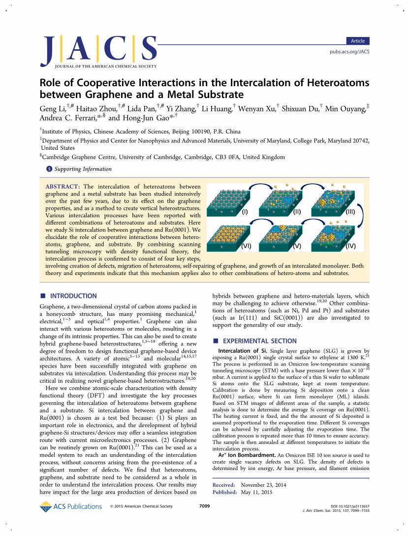
■ RESULTS AND DISCUSSIONFigure 1a plots a 90 × 90 nm STM topographic image ofgraphene after partial intercalation of Si. Before Si intercalation,
intact SLG can be seen (see Supporting Information FigureS1).21 Figure 1a shows a smooth and flat surface that can beassigned as SLG/Si/Ru with a Si ML between the SLG and Ru.The rest of the image is a region with a small percentage of Si,as evidenced by the appearance of small isolated Si islandsunderneath graphene, with a line profile shown in Figure 1b.The high-resolution image in Figure 1c further reveals that theSLG is intact and uniform after Si intercalation, which isconfirmed by both STM characterization on different samplelocations and Raman spectroscopy25 (see Supporting Informa-tion Figure S2).A few mechanisms have been proposed to account for similar
intercalation processes.7,11,14,16,18 Heteroatoms can diffusethrough graphene island edges or pre-existing defects7,11,14,18
or exchange with carbon atoms.16 However, these mechanismsdo not explain our observations, since our SLG has negligiblepre-existing defects.21 Previous low-energy electron microscopystudies16 suggested that the Si atoms could directly penetratethrough SLG without requirement of edges14 or wrinkles.18
But, the temperature in our experiments is not enough to breakthe carbon−carbon bond (the bond energy was estimated to be∼5.67 eV,26 corresponding to a temperature of ∼6.6 × 10⁴ K)or to enable the Si−C exchange process, requiring at least 3eV.16
Figure 1d outlines our proposed mechanism by highlightinga few key steps: cooperative creation of defects (stage II),migration of heteroatoms through graphene to the Ru surface(stage III), self-repair of the graphene lattice (stage IV), andassembly of heteroatoms to form an intercalated layer (stageV). These four steps are intercorrelated and can happensimultaneously, which makes it challenging for unambiguouscharacterization.Figure 2a shows a typical image after deposition of 0.05 ML
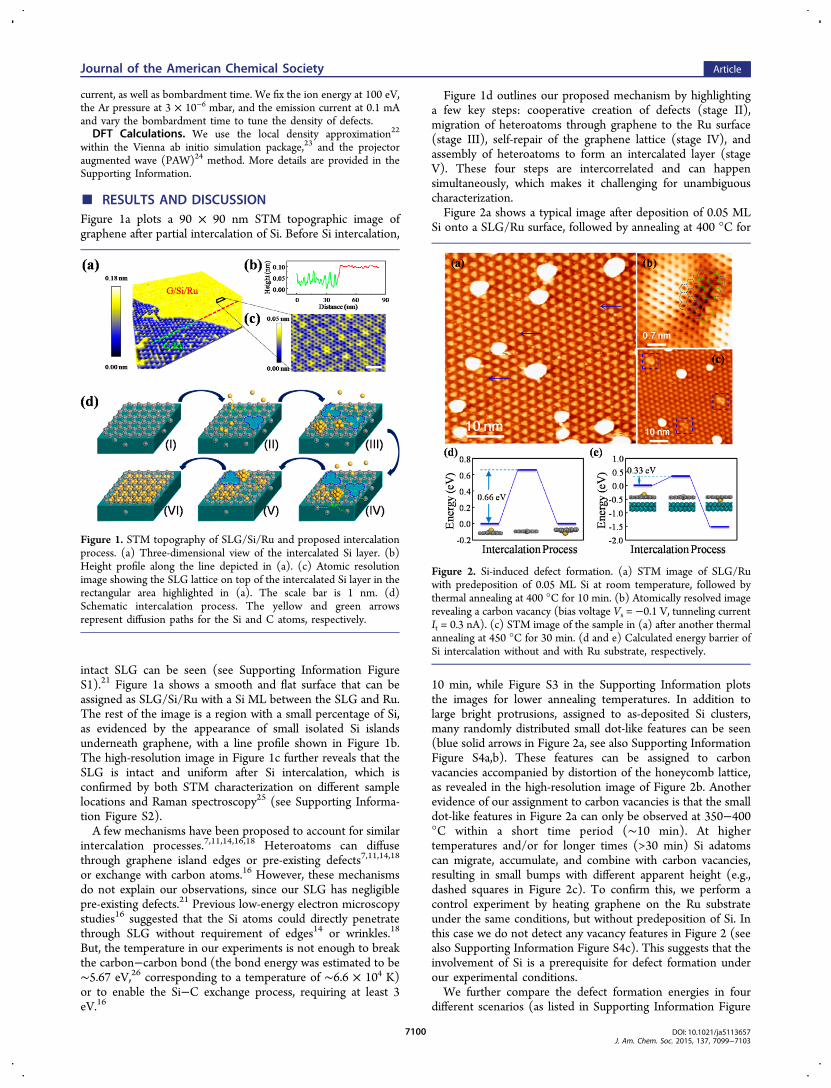
Si onto a SLG/Ru surface, followed by annealing at 400 °C for
10 min, while Figure S3 in the Supporting Information plotsthe images for lower annealing temperatures. In addition tolarge bright protrusions, assigned to as-deposited Si clusters,many randomly distributed small dot-like features can be seen(blue solid arrows in Figure 2a, see also Supporting InformationFigure S4a,b). These features can be assigned to carbonvacancies accompanied by distortion of the honeycomb lattice,as revealed in the high-resolution image of Figure 2b. Anotherevidence of our assignment to carbon vacancies is that the smalldot-like features in Figure 2a can only be observed at 350−400°C within a short time period (∼10 min). At highertemperatures and/or for longer times (>30 min) Si adatomscan migrate, accumulate, and combine with carbon vacancies,resulting in small bumps with different apparent height (e.g.,dashed squares in Figure 2c). To confirm this, we perform acontrol experiment by heating graphene on the Ru substrateunder the same conditions, but without predeposition of Si. Inthis case we do not detect any vacancy features in Figure 2 (seealso Supporting Information Figure S4c). This suggests that theinvolvement of Si is a prerequisite for defect formation underour experimental conditions.We further compare the defect formation energies in four
different scenarios (as listed in Supporting Information Figure
Figure 1. STM topography of SLG/Si/Ru and proposed intercalationprocess. (a) Three-dimensional view of the intercalated Si layer. (b)Height profile along the line depicted in (a). (c) Atomic resolutionimage showing the SLG lattice on top of the intercalated Si layer in therectangular area highlighted in (a). The scale bar is 1 nm. (d)Schematic intercalation process. The yellow and green arrowsrepresent diffusion paths for the Si and C atoms, respectively.
Figure 2. Si-induced defect formation. (a) STM image of SLG/Ruwith predeposition of 0.05 ML Si at room temperature, followed bythermal annealing at 400 °C for 10 min. (b) Atomically resolved imagerevealing a carbon vacancy (bias voltage Vs = −0.1 V, tunneling currentIt = 0.3 nA). (c) STM image of the sample in (a) after another thermalannealing at 450 °C for 30 min. (d and e) Calculated energy barrier ofSi intercalation without and with Ru substrate, respectively.
Journal of the American Chemical Society Article
DOI: 10.1021/ja5113657J. Am. Chem. Soc. 2015, 137, 7099−7103
7100
S5) by ab initio calculations:27 free-standing SLG, SLG/Ru,free-standing SLG with a Si adatom, and SLG/Ru with a Siadatom. An energy reduction from 8.09 eV (free-standing SLG)to 0.23 eV (Si-SLG-Ru) is observed after inclusion ofinteractions between Si adatoms, graphene, and substrate,making it possible to create vacancies in our experimentalconditions.The availability of carbon vacancies can thus facilitate
migration of Si atoms through SLG. In order to evaluate therole of defects, we also perform a control experiment bycreating single vacancy defects by low-energy ion bombard-ment.28 Argon ions with an energy of 100 eV can create singlevacancy defects on SLG/Ru, with defect density controllable bychanging the dosage and duration (Supporting InformationFigures S6 and S7). The same amount (2 ML) of Si isdeposited onto SLG/Ru samples with different initial defectdensity (Supporting Information Figure S6a−c), followed byannealing at 700 °C for 30 min. The higher the initial defectdensity, the more Si can be intercalated (SupportingInformation Figure S6d−f), suggesting that defects indeedenable and promote intercalation, supporting the proposeddefect assisted intercalation process.In order to evaluate the role of the substrate in the
intercalation process, we employ the climb nudged elastic bandmethod29 to simulate migration of a single Si atom through avacancy. Figure 2d,e compares the energy barrier difference forthe migration process without and with consideration of theeffect of Ru(0001). We observe a significant reduction of thebarrier from 0.66 eV (without substrate) to 0.33 eV (withsubstrate), suggesting that the Ru substrate can further reducethe energy barrier of this process, as well as the total energy ofthe system, during Si intercalation. This effect also makes theinverse process (i.e., migration of Si atoms from the interface tothe upper SLG surface) less likely under our experimentalconditions.We observe that the honeycomb carbon lattice can be
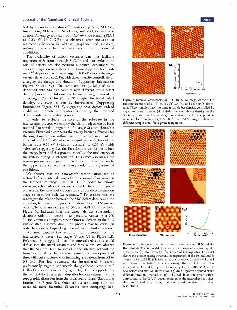
restored after Si intercalation, with the removal of vacancies inthe temperature range 300−800 °C. In order to removevacancies, extra carbon atoms are required. These can originateeither from the knockout carbon atoms in the defect formationstage or from the bulk Ru substrate.30 To confirm this, weinvestigate the relation between the SLG defect density and theannealing temperature. Figure 3a−c shows three STM imagesof SLG/Ru after annealing at 25, 300, and 450 °C, respectively.Figure 3d indicates that the defect density substantiallydecreases with the increase in temperature. Annealing at 700°C for 30 min is enough to repair almost all defects on the SLGsurface after Si intercalation. This process may be critical inorder to create high-quality graphene-based hybrid structures.We now explore the evolution and assembly of the
intercalated Si layer (i.e., stages V and VI in Figure 1d).Reference 31 suggested that the intercalated atoms coulddiffuse into the metal substrate and form alloys. We observethat the Si atoms tend to spread at the interface without theformation of alloys. Figure 4a−c shows the development ofthree different structures with increasing Si adatoms from 0.3 to0.8 ML. For low coverage, the intercalated Si atomspreferentially migrate underneath the graphene’s atop sites32
(hills of the moire structure) (Figure 4a). This is supported bythe fact that the intercalated atop sites become enlarged, with atopographic distortion from the usual round shape (SupportingInformation Figure S1). Once all available atop sites areoccupied, more incoming Si atoms start occupying face-
Figure 3. Removal of vacancies on SLG/Ru. STM images of the SLG/Ru samples annealed at (a) 25 °C, (b) 300 °C, and (c) 450 °C for 30min. These samples have the same initial defect density, controlled byargon ion bombardment. (d) Relation between defect density on theSLG/Ru surface and annealing temperature. Each data point isobtained by averaging eight 50 × 50 nm STM images taken ondifferent sample areas for a given temperature.
Figure 4. Evolution of the intercalated Si layer between SLG and theRu substrate.The intercalated Si atoms can sequentially occupy theareas below (a) atop sites, (b) fcc sites, and (c) hcp sites. The insetshows the corresponding structural configuration of the intercalated Siatoms. (d) A full ML Si is formed at the interface. Inset is a 4.5 × 4.5nm atomic resolution image showing the SLG lattice afterintercalation. (e and f) Typical topography (Vs = −0.05 V, It = 1.0nA) before and after Si intercalation. (g) dI/dV spectra acquired at thedifferent locations marked in (f). The red, blue, and green curvescorrespond to the dI/dV spectra acquired at the intercalated fcc sites,the intercalated atop sites, and the non-intercalated fcc sites,respectively.
Journal of the American Chemical Society Article
DOI: 10.1021/ja5113657J. Am. Chem. Soc. 2015, 137, 7099−7103
7101
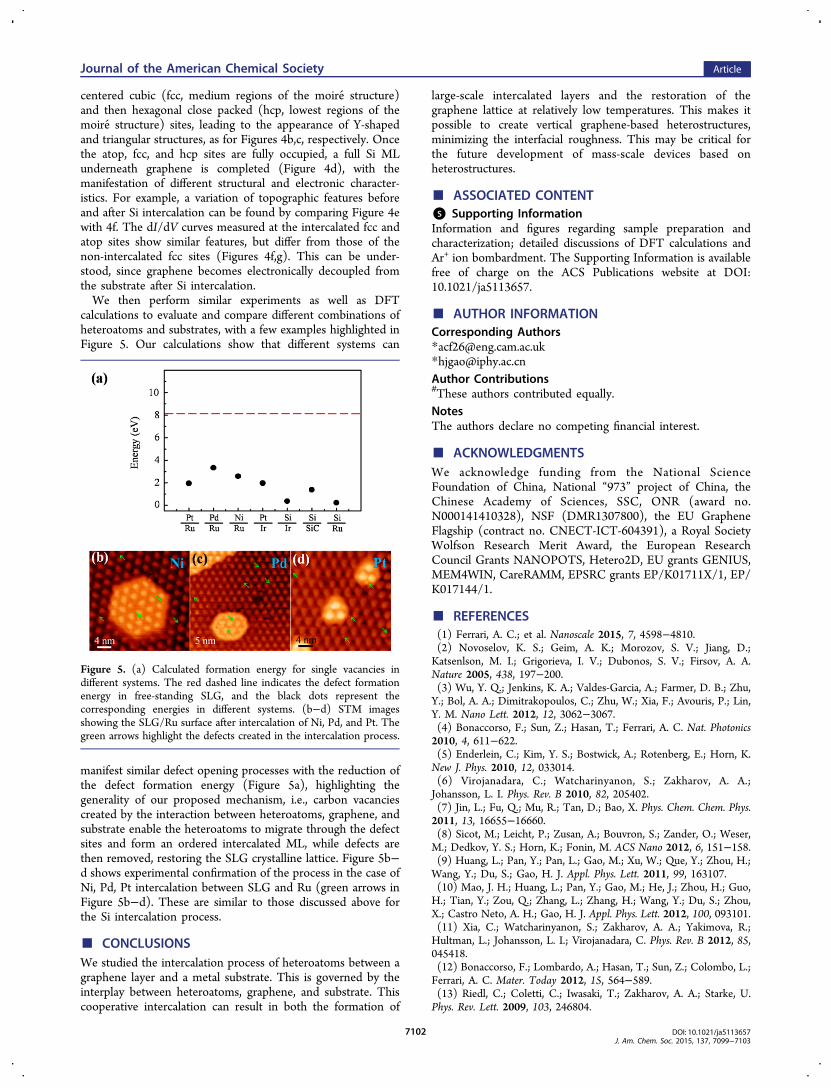
centered cubic (fcc, medium regions of the moire structure)and then hexagonal close packed (hcp, lowest regions of themoire structure) sites, leading to the appearance of Y-shapedand triangular structures, as for Figures 4b,c, respectively. Oncethe atop, fcc, and hcp sites are fully occupied, a full Si MLunderneath graphene is completed (Figure 4d), with themanifestation of different structural and electronic character-istics. For example, a variation of topographic features beforeand after Si intercalation can be found by comparing Figure 4ewith 4f. The dI/dV curves measured at the intercalated fcc andatop sites show similar features, but differ from those of thenon-intercalated fcc sites (Figures 4f,g). This can be under-stood, since graphene becomes electronically decoupled fromthe substrate after Si intercalation.We then perform similar experiments as well as DFT
calculations to evaluate and compare different combinations ofheteroatoms and substrates, with a few examples highlighted inFigure 5. Our calculations show that different systems can
manifest similar defect opening processes with the reduction ofthe defect formation energy (Figure 5a), highlighting thegenerality of our proposed mechanism, i.e., carbon vacanciescreated by the interaction between heteroatoms, graphene, andsubstrate enable the heteroatoms to migrate through the defectsites and form an ordered intercalated ML, while defects arethen removed, restoring the SLG crystalline lattice. Figure 5b−d shows experimental confirmation of the process in the case ofNi, Pd, Pt intercalation between SLG and Ru (green arrows inFigure 5b−d). These are similar to those discussed above forthe Si intercalation process.
■ CONCLUSIONSWe studied the intercalation process of heteroatoms between agraphene layer and a metal substrate. This is governed by theinterplay between heteroatoms, graphene, and substrate. Thiscooperative intercalation can result in both the formation of
large-scale intercalated layers and the restoration of thegraphene lattice at relatively low temperatures. This makes itpossible to create vertical graphene-based heterostructures,minimizing the interfacial roughness. This may be critical forthe future development of mass-scale devices based onheterostructures.
■ ASSOCIATED CONTENT*S Supporting InformationInformation and figures regarding sample preparation andcharacterization; detailed discussions of DFT calculations andAr+ ion bombardment. The Supporting Information is availablefree of charge on the ACS Publications website at DOI:10.1021/ja5113657.
■ AUTHOR INFORMATIONCorresponding Authors*[email protected]*[email protected] Contributions#These authors contributed equally.NotesThe authors declare no competing financial interest.
■ ACKNOWLEDGMENTSWe acknowledge funding from the National ScienceFoundation of China, National “973” project of China, theChinese Academy of Sciences, SSC, ONR (award no.N000141410328), NSF (DMR1307800), the EU GrapheneFlagship (contract no. CNECT-ICT-604391), a Royal SocietyWolfson Research Merit Award, the European ResearchCouncil Grants NANOPOTS, Hetero2D, EU grants GENIUS,MEM4WIN, CareRAMM, EPSRC grants EP/K01711X/1, EP/K017144/1.
■ REFERENCES(1) Ferrari, A. C.; et al. Nanoscale 2015, 7, 4598−4810.(2) Novoselov, K. S.; Geim, A. K.; Morozov, S. V.; Jiang, D.;Katsenlson, M. I.; Grigorieva, I. V.; Dubonos, S. V.; Firsov, A. A.Nature 2005, 438, 197−200.(3) Wu, Y. Q.; Jenkins, K. A.; Valdes-Garcia, A.; Farmer, D. B.; Zhu,Y.; Bol, A. A.; Dimitrakopoulos, C.; Zhu, W.; Xia, F.; Avouris, P.; Lin,Y. M. Nano Lett. 2012, 12, 3062−3067.(4) Bonaccorso, F.; Sun, Z.; Hasan, T.; Ferrari, A. C. Nat. Photonics2010, 4, 611−622.(5) Enderlein, C.; Kim, Y. S.; Bostwick, A.; Rotenberg, E.; Horn, K.New J. Phys. 2010, 12, 033014.(6) Virojanadara, C.; Watcharinyanon, S.; Zakharov, A. A.;Johansson, L. I. Phys. Rev. B 2010, 82, 205402.(7) Jin, L.; Fu, Q.; Mu, R.; Tan, D.; Bao, X. Phys. Chem. Chem. Phys.2011, 13, 16655−16660.(8) Sicot, M.; Leicht, P.; Zusan, A.; Bouvron, S.; Zander, O.; Weser,M.; Dedkov, Y. S.; Horn, K.; Fonin, M. ACS Nano 2012, 6, 151−158.(9) Huang, L.; Pan, Y.; Pan, L.; Gao, M.; Xu, W.; Que, Y.; Zhou, H.;Wang, Y.; Du, S.; Gao, H. J. Appl. Phys. Lett. 2011, 99, 163107.(10) Mao, J. H.; Huang, L.; Pan, Y.; Gao, M.; He, J.; Zhou, H.; Guo,H.; Tian, Y.; Zou, Q.; Zhang, L.; Zhang, H.; Wang, Y.; Du, S.; Zhou,X.; Castro Neto, A. H.; Gao, H. J. Appl. Phys. Lett. 2012, 100, 093101.(11) Xia, C.; Watcharinyanon, S.; Zakharov, A. A.; Yakimova, R.;Hultman, L.; Johansson, L. I.; Virojanadara, C. Phys. Rev. B 2012, 85,045418.(12) Bonaccorso, F.; Lombardo, A.; Hasan, T.; Sun, Z.; Colombo, L.;Ferrari, A. C. Mater. Today 2012, 15, 564−589.(13) Riedl, C.; Coletti, C.; Iwasaki, T.; Zakharov, A. A.; Starke, U.Phys. Rev. Lett. 2009, 103, 246804.
Figure 5. (a) Calculated formation energy for single vacancies indifferent systems. The red dashed line indicates the defect formationenergy in free-standing SLG, and the black dots represent thecorresponding energies in different systems. (b−d) STM imagesshowing the SLG/Ru surface after intercalation of Ni, Pd, and Pt. Thegreen arrows highlight the defects created in the intercalation process.
Journal of the American Chemical Society Article
DOI: 10.1021/ja5113657J. Am. Chem. Soc. 2015, 137, 7099−7103
7102

(14) Sutter, P.; Sadowski, J. T.; Sutter, E. A. J. Am. Chem. Soc. 2010,132, 8175−8179.(15) Feng, X. F.; Maier, S.; Salmeron, M. J. Am. Chem. Soc. 2012, 134,5662−5668.(16) Cui, Y.; Gao, J.; Jin, L.; Zhao, J.; Tan, D.; Fu, Q.; Bao, X. NanoRes. 2012, 5, 352−360.(17) Zhao, W.; Tan, P. H.; Liu, J.; Ferrari, A. C. J. Am. Chem. Soc.2011, 133, 5941−5946.(18) Petrovic, M.; Srut Rakic, I.; Runte, S.; Busse, C.; Sadowski, J. T.;Lazic, P.; Pletikosic, I.; Pan, Z.-H.; Milun, M.; Pervan, P.; Atodiresei,N.; Brako, R.; Sokcevic, D.; Valla, T.; Michely, T.; Kralj, M. Nat.Commun. 2013, 4, 2772.(19) Britnell, L.; Gorbachev, R. V.; Jalil, R.; Belle, B. D.; Schedin, F.;Mishchenko, A.; Georgiou, T.; Katsnelson, M. I.; Eaves, L.; Morozov,S. V.; Peres, N. M. R.; Leist, J.; Geim, A. K.; Novoselov, K. S.;Ponomarenko, L. A. Science 2012, 335, 947−950.(20) Haigh, S. J.; Gholinia, A.; Jalil, R.; Romani, S.; Britnell, L.; Elias,D. C.; Novoselov, K. S.; Ponomarenko, L. A.; Geim, A. K.; Gorbachev,R. Nat. Mater. 2012, 11, 764−767.(21) Pan, Y.; Zhang, H.; Shi, D.; Sun, J.; Du, S.; Liu, F.; Gao, H. J.Adv. Mater. 2009, 21, 2777−2780.(22) Perdew, J. P.; Zunger, A. Phys. Rev. B 1981, 23, 5048−5079.(23) Kresse, G.; Furthmuller, J. Phys. Rev. B 1996, 54, 11169−11186.(24) Blochl, P. E. Phys. Rev. B 1994, 50, 17953−17979.(25) Ferrari, A. C.; Basko, D. M. Nat. Nanotechnol. 2013, 8, 235−246.(26) Girit, C. O.; Meyer, J. C.; Erni, R.; Rossell, M. D.; Kisielowski,C.; Yang, L.; Park, C.-H.; Crommie, M. F.; Cohen, M. L.; Louie, S. G.;Zettl, A. Science 2009, 323, 1705−1708.(27) Wang, L.; Zhang, X.; Chan, H. L. W.; Yan, F.; Ding, F. J. Am.Chem. Soc. 2013, 135, 4476−4482.(28) Ugeda, M. M.; Brihuega, I.; Guinea, F.; Gomez-Rodríguez, J. M.Phys. Rev. Lett. 2010, 104, 096804.(29) Henkelman, G.; Uberuaga, B. P.; Jonsson, H. A. J. Chem. Phys.2000, 113, 9901−9904.(30) Cui, Y.; Fu, Q.; Bao, X. Phys. Chem. Chem. Phys. 2010, 12,5053−5057.(31) Vilkov, O.; Fedorov, A.; Usachov, D.; Yashina, L. V.; Generalov,A. V.; Borygina, K.; Verbitskiy, N. I.; Gruneis, A.; Vyalikh, D. V. Sci.Rep. 2013, 3, 2168.(32) Zhou, H. T.; Mao, J. H.; Li, G.; Wang, Y. L.; Feng, X. L.; Du, S.X.; Mullen, K.; Gao, H. J. Appl. Phys. Lett. 2011, 99, 153101.
■ NOTE ADDED AFTER ASAP PUBLICATIONThe uncorrected proof version was published ASAP on May 18,2015. The final corrected version was published on May 29,2015.
Journal of the American Chemical Society Article
DOI: 10.1021/ja5113657J. Am. Chem. Soc. 2015, 137, 7099−7103
7103