hardware/software codesign approaches to public …
TRANSCRIPT

HARDWARE/SOFTWARE CODESIGN APPROACHES TO PUBLIC KEY
CRYPTOSYSTEMS
by
Malik Umar Sharif
A Dissertation
Submitted to the
Graduate Faculty
of
George Mason University
in Partial Fulfillment of
The Requirements for the Degree
of
Doctor of Philosophy
Electrical and Computer Engineering
Committee:
______________________________ Dr. Kris Gaj, Dissertation Director
______________________________ Dr. Jens Peter Kaps, Committee Member
______________________________ Dr. Houman Homayoun, Committee Member
______________________________ Dr. Robert Simon, Committee Member
______________________________ Dr. Monson H. Hayes, Department Chair
______________________________ Dr. Kenneth S. Ball, Dean, Volgenau School
of Engineering
Date: __________________________ Summer Semester 2017
George Mason University
Fairfax, VA
ii
Hardware/Software Codesign Approaches to Public Key Cryptosystems
A Dissertation submitted in partial fulfillment of the requirements for the degree of
Doctor of Philosophy at George Mason University
by
Malik Umar Sharif
Master of Science
George Washington University, 2010
Bachelor of Science
National University of Sciences and Technology, 2001
Director: Kris Gaj, Associate Professor
Department of Electrical and Computer Engineering
Summer Semester 2017
George Mason University
Fairfax, VA
x
Copyright 2017 Malik Umar Sharif
All Rights Reserved

xi
DEDICATION
I dedicate this dissertation to my lovely wife, Rabia. It would not have been possible
without her consistent support as a partner all these years. To my mother, who has
always been there for me whenever I needed guidance and her prayers have always
kept me going. I would also like to dedicate this to my father for always believing in me
and lastly to my son, Shaheer. He has always brightened my day with his smile and has
been the reason for my motivation specially in the past couple of years.

xii
ACKNOWLEDGEMENTS
I would specially like to acknowledge and express my sincere gratitude towards my
advisor Dr. Kris Gaj for his consistent guidance, knowledge and mentorship during my
Ph.D study and research. It has always been a pleasure working under his supervision.
His attention to detail and thorough knowledge has helped me immensely to accomplish
the research work I have worked on.
I would also like to thank Dr. Kaps for always giving great feedback whenever I asked
for any guidance. He has always been open to new ideas and insight related to any
challenges I faced during my Ph.D.
I would also like to thank my other committee members, Dr. Houman Homayoun and
Dr. Simon for their valuable comments regarding my thesis study.
I would also extend my gratitude to all fellow present and former Cryptographic
Engineering Research Group (CERG) members for all the discussions, meetings and
valuable feedback they offered throughout these years.
And in the end, a special thanks to all my family members, my parents, my sister, and
my wife Rabia for always being there for me whenever I needed them the most.

xiii
TABLE OF CONTENTS
Page LIST OF TABLES………………………………………………………………………. viii
LIST OF FIGURES…………………………………………………………………….. x
ABSTRACT……………………………………………………………………………. xi
1 INTRODUCTION ............................................................................................................. 1
1.1 Traditional and Post-Quantum Public Key Cryptography ......................................... 1
1.2 Motivation and Research Goals ................................................................................. 6
1.2.1 Post-Quantum Cryptosystems (PQC) ................................................................ 7
1.2.2 Hardware/ Software Codesign ........................................................................... 8
1.2.3 Zynq All Programmable System on Chip .......................................................... 8
1.2.4 Research Questions & Challenges ................................................................... 10
2 BACKGROUND ............................................................................................................. 11
2.1 Cryptographic Algorithms ....................................................................................... 11
2.1.1 RSA .................................................................................................................. 11
2.1.2 Lattice-Based Cryptosystems ........................................................................... 15
2.1.3 NTRUEncrypt Cryptosystem ........................................................................... 18
2.2 Technology .............................................................................................................. 20
2.2.1 Hardware/Software Codesign Platforms .......................................................... 20
2.2.2 Hardware/Software Codesign with Xilinx Zynq SoC ...................................... 23
2.2.3 Type of AXI Interfaces in Zynq SoC ............................................................... 29
2.2.4 AXI DMA ........................................................................................................ 32
2.2.5 Embedded FPGA Resources ............................................................................ 32
3 SURVEY OF PREVIOUS WORK .................................................................................. 36
3.1 HW/ SW Codesign Implementations of RSA .......................................................... 36
3.2 Previous HW/ SW Codesign Implementations on Traditional Public-Key
Cryptography ....................................................................................................................... 39
3.3 Previous Implementations of Lattice Based Cryptosystems .................................... 43
3.3.1 Previous Implementations of NTRU Cryptosystem ........................................ 43
3.3.2 Previous Implementations on Modular Multiplier Designs ............................. 45
4 HARDWARE/SOFTWARE CODESIGN OF RSA ........................................................ 47
4.1 Software Development ............................................................................................. 47
4.1.1 Developing and Extending Software APIs in RELIC Library ......................... 47
4.1.2 Hardware/Software Partitioning ...................................................................... 48
xiv
4.2 Operation of the Processing System ........................................................................ 49
4.3 Choice of Communication Interface ........................................................................ 53
4.4 Implementing Programmable Logic (PL) – Our Hardware Accelerator .................. 54
4.5 Results and Comparison .......................................................................................... 58
4.6 Conclusion ............................................................................................................... 63
5 CUSTOM HARDWARE IMPLEMENTATION OF NTRUEncrypt .............................. 64
5.1 Preliminaries ............................................................................................................ 64
5.2 NTRUEncrypt SVES ............................................................................................... 65
5.3 Hardware Design ..................................................................................................... 69
5.3.1 Hardware API & Interface of NTRU core ....................................................... 71
5.3.2 Top-Level Block Diagram ............................................................................... 72
5.3.3 Diagrams of Selected Lower-Level Components ............................................ 76
5.4 Results ...................................................................................................................... 79
5.5 Conclusions .............................................................................................................. 85
6 Hardware/ Software Codesign of NTRUEncrypt ............................................................ 87
6.1 Methodology ............................................................................................................ 87
6.2 Software Profiling .................................................................................................... 88
6.3 Proposed Partitioning Schemes:............................................................................... 88
6.4 Four popssible partitioning schemes NTRUEncrypt bewteen software and hardware
6.5 Optimizing the Polynomial Multiplier ..................................................................... 91
6.6 Conclusion ............................................................................................................. 100
6.7 Future Work ........................................................................................................... 100
7 CONCLUSIONS & FUTURE WORK .......................................................................... 101
7.1 Possibilities for Future Work ................................................................................. 103
A. PUBLICATIONS ........................................................................................................... 105

xv
LIST OF TABLES
Table Page
Table 1. Short History of Quantum Computing..................................................... 3
Table 2. Comparison with Alternative Solutions (Source: Xilinx Video Tutorials)
...................................................................................................................... 10
Table 3 The Underlying Security Problem and the Best Known Algorithms for
Solving this Problem .................................................................................... 16
Table 4 Major Algorithms of Lattice-based cryptosystems and their Publication
Dates ............................................................................................................ 17
Table 5. Public Key Sizes for Lattice-based algorithms for selected Security
Levels. .......................................................................................................... 18
Table 6. Communication Interface Options in Zync SoC.................................... 29
Table 7. HW/ SW Codesign Implementations of RSA........................................ 38
Table 8. HW/ SW Codesign Implementations of ECC for 80-bit security. ......... 40
Table 9. Selected Hardware Implementations of NTRU ..................................... 45
Table 10. Implemented hardware functions ......................................................... 50
Table 11. Comparison of our HW/SW Implementation with software
implementation based on RELIC for four operand sizes and three
exponentiation schemes. Note: CCpre – Clock cucles for preprocessing,
CCpost – Clock cycles for postprocessing, CCproc – Clock cycles for
processing, CCsw – Clock cycles for software, CChw/sw – Clock cycles for
HW/SW codesign......................................................................................... 60
Table 12. Comparison of our work with existing designs of modular
exponentiation ME from literature. Note: * - the execution time was
determined for the ME scheme and operand size marked by this symbol,
SLID – Sliding Window Method, MPL – Montgomer Powering Ladder,
BFL – Blinded Fault Resistant Exponentiation ........................................... 61
Table 13. Basic operations of Encryption and Decryption. ................................. 66
Table 14. Inputs, Outputs, and Intermediate Variables ....................................... 67
Table 15. Parameters of the algorithm, architecture, and input affecting the
execution time, for two parameter sets ees1499ep1 and ees1087ep1. ......... 70
Table 16. Auxiliary components used in the top-level block diagram and the
diagrams of lower-level components. .......................................................... 73
Table 17. Resource utilization and performance metrics of major component
units. Latencies correspond to the ees1499ep1 parameter set. .................... 80
Table 18. Timing analysis of our hardware implementation. Latencies in clock
cycles correspond to the maximum sizes of messages allowed by a given
parameter set. ............................................................................................... 81
Table 19. Results of profiling of the software implementation of NTRUEncrypt
SVES from [9], using the Cortex A9 ARM Core of Zynq 7020, for the
ees1499ep1parameter set ............................................................................. 82
Table 20. Speed up of Hardware (This Work) vs. Software (source code [54]) . 83

xvi
Table 21. Previous Hardware Implementations of NTRU. Notation: E –
encryption, D – decryption, E/D: Encryption & Decryption. ...................... 84
Table 22. Comparison of the results for the hardware implementation of Poly
Mult by Liu et al. using Altera Cyclone IV, and this work using Xilinx
Kintex-7. ...................................................................................................... 84
Table 23. Comparison of Results with and without Pipelining at different
Pipeline Levels ............................................................................................. 96
Table 24. Results of profiling of the software implementation of NTRUEncrypt
SVES, using the Cortex A9 ARM Core of Zynq 7020, for the ees401ep1
parameter set ................................................................................................ 97
Table 25. Results of profiling of the HW/ SW codesign implementation of
NTRUEncrypt SVES, using the Cortex A9 ARM Core of Zynq 7020, for
the ees401ep1 parameter set ........................................................................ 98
Table 26. Results of profiling of the hardware implementation of NTRUEncrypt
SVES, using the Cortex A9 ARM Core of Zynq 7020, for the ees401ep1
parameter set ................................................................................................ 99
Table 27 . Timing analysis of our HW/ SW codesign implementation. Latencies
in clock cycles correspond to the maximum sizes of messages allowed by a
given parameter set. ..................................................................................... 99

xvii
LIST OF FIGURES
Figure Page
Figure 1. Scope of Research .......................................................................................... 2
Figure 2. Discrete FPGA-Processor Combination ....................................................... 21
Figure 3. Zync SoC Z7020 platform with interface between PS and PL .................... 25
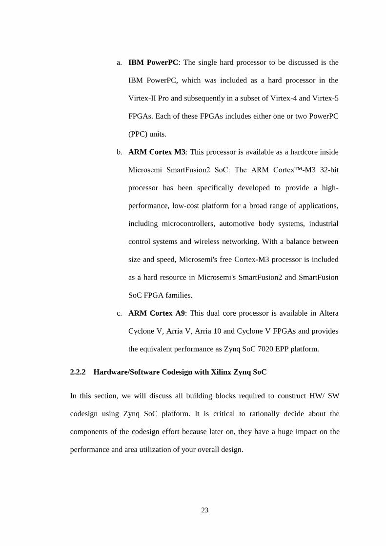
Figure 4. SIPO in Input interface of Coprocessor........................................................ 26
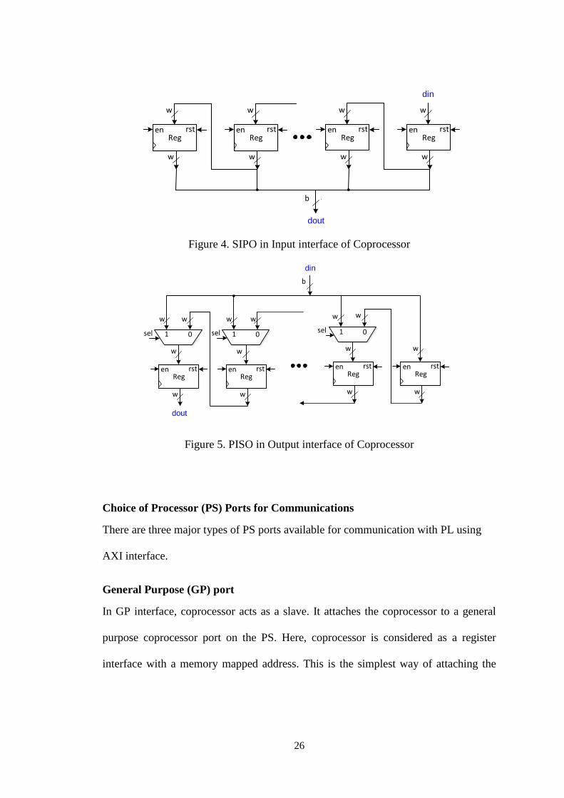
Figure 5. PISO in Output interface of Coprocessor ..................................................... 26
Figure 6. Processor Ports for Communication between PS and PL ............................. 28
Figure 7. AXI Interfaces .............................................................................................. 29
Figure 8. AXI-Lite Interface ........................................................................................ 30
Figure 9. AXI Full Interface ........................................................................................ 31
Figure 10. AXI Stream Interface ................................................................................. 31
Figure 11. DSP48 inside Zync SoC Z7020 and Latency selection to operate at 400
MHz ..................................................................................................................... 33
Figure 12. True Dual Port BRAM to store input data.................................................. 34
Figure 13. Hierarchy of Operations and Tentative Partitioning Schemes in RSA ...... 48
Figure 14. Detailed Hardware Coprocessor Design .................................................... 56
Figure 15. Flow diagram of SVES Encryption (top) and Decryption (bottom) .......... 66
Figure 16. NTRU Interface compatible with the PQC Hardware API interface [8].... 71
Figure 17. Top-level block diagram of the developed hardware architecture of SVES.
N represents max(1499, 1087)=1499. .................................................................. 74
Figure 18. Architecture of the polynomial multiplier, folded by a factor of 3 ............ 78
Figure 19. Hardware architecture of the combined unit, BPGM/MGF, implementing
the Blinding Polynomial Generation Method and Mask Generation Function ... 79
Figure 20. Partitioning Schemes for HW/ SW Codesign of NTRU ............................ 89
Figure 21. Interface for Polynomial Multiplier............................................................ 90
Figure 22. Polynomial Multiplier – Full Version ........................................................ 92
Figure 23. Critical Path Analysis for Polynomial Multiplier ....................................... 93
Figure 24. Full version of the multiplier (Critical Path shown in Red). ....................... 94
Figure 25. Diagram for Pipelining at different Pipeline Levels ................................... 94
Figure 26. Polynomial Multiplier – Folded Architecture ............................................. 95
Figure 27. Reconfigurable Resource Utilization of Zynq SoC for HW/ SW Codesign
Implementation .................................................................................................... 97
xviii
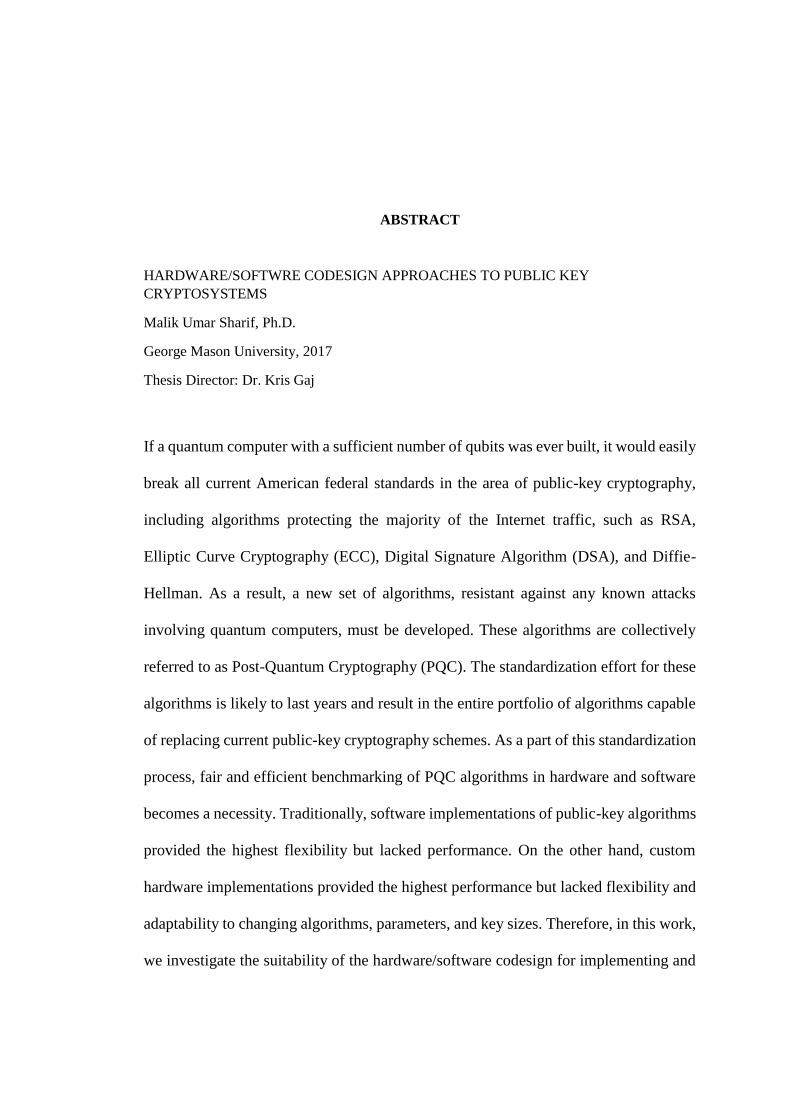
ABSTRACT
HARDWARE/SOFTWRE CODESIGN APPROACHES TO PUBLIC KEY
CRYPTOSYSTEMS
Malik Umar Sharif, Ph.D.
George Mason University, 2017
Thesis Director: Dr. Kris Gaj
If a quantum computer with a sufficient number of qubits was ever built, it would easily
break all current American federal standards in the area of public-key cryptography,
including algorithms protecting the majority of the Internet traffic, such as RSA,
Elliptic Curve Cryptography (ECC), Digital Signature Algorithm (DSA), and Diffie-
Hellman. As a result, a new set of algorithms, resistant against any known attacks
involving quantum computers, must be developed. These algorithms are collectively
referred to as Post-Quantum Cryptography (PQC). The standardization effort for these
algorithms is likely to last years and result in the entire portfolio of algorithms capable
of replacing current public-key cryptography schemes. As a part of this standardization
process, fair and efficient benchmarking of PQC algorithms in hardware and software
becomes a necessity. Traditionally, software implementations of public-key algorithms
provided the highest flexibility but lacked performance. On the other hand, custom
hardware implementations provided the highest performance but lacked flexibility and
adaptability to changing algorithms, parameters, and key sizes. Therefore, in this work,
we investigate the suitability of the hardware/software codesign for implementing and
xix
evaluating traditional and post-quantum public-key cryptosystems from the point of
view of their implementation efficiency.
As our case studies, we considered one traditional public key cryptosystem, RSA, and
one post-quantum public key cryptosystem, NTRUEncrypt. We implemented both of
them using custom hardware, as well as software/hardware codesign. The Xilinx Zynq-
7000 System on Chip platform, which integrates a dual-core ARM Cortex A9
processing system along with Xilinx programmable logic, was used for our
experiments. The performance vs. flexibility trade-off has been investigated, and the
speed-up of our software/hardware codesign implementations vs. the purely software
implementations on the same platform is reported and analyzed. Similarly, the speed-
up of the custom hardware vs. hardware-software codesign is investigated as well.
Additionally, we have determined and analyzed different percentage contributions of
the execution times for equivalent component operations executed using the
aforementioned three different implementation approaches (custom hardware,
software/hardware codesign, and pure software). We demonstrate that
hardware/software codesign can reliably assist in early evaluation and comparison of
various public-key cryptography schemes. Our project is intended to pave the way for
the future comprehensive, fair, and efficient benchmarking of the most promising
encryption, signature, and key agreement schemes from each of several major post-
quantum public-key cryptosystem families.
1
1 INTRODUCTION
In this chapter, we describe the existing traditional and post-quantum public key
cryptosystems that are used in the field of cryptography and reported in the literature.
We also provide the motivation behind working on post-quantum public key
cryptosystems and the reason why cryptographic community should focus its attention
on preparing for the next generation of quantum resistant algorithms. We also
emphasize on the importance of choosing the hardware/software codesign platform in
an effort to evaluate and benchmark these algorithms and reasons to choose Xilinx
system on chip solution to implement the designs and analyze the results.
1.1 Traditional and Post-Quantum Public Key Cryptography
The idea of Public-Key Cryptography (PKC) was proposed by Diffie and Hellman in
1976 [1]. Later during the next year Ron Rivest, Adi Shamir and Leonard Addleman
[2] proposed another public-key cryptosystem known as RSA which enabled
encryption of a message using public key of the receiver. Only the receiver could
decrypt the message with its private key which is kept as a secret.
Public-key cryptosystems simplified the issue of key management. As they require
intense mathematical calculations based on integer factorization and discrete
logarithms, the implementations were much slower than symmetric key algorithms for
encryption. As a result, secret-key cryptography kept on being in use for bulk
encryption, while public-key cryptosystems were used for key management. With the
advancements in the computing power of modern computers and due to efficient
algorithms for integer factorization, the increasing size of RSA modulus caused the
implementations to become slower due to large key sizes.
2
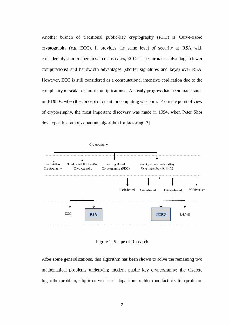
Another branch of traditional public-key cryptography (PKC) is Curve-based
cryptography (e.g. ECC). It provides the same level of security as RSA with
considerably shorter operands. In many cases, ECC has performance advantages (fewer
computations) and bandwidth advantages (shorter signatures and keys) over RSA.
However, ECC is still considered as a computational intensive application due to the
complexity of scalar or point multiplications. A steady progress has been made since
mid-1980s, when the concept of quantum computing was born. From the point of view
of cryptography, the most important discovery was made in 1994, when Peter Shor
developed his famous quantum algorithm for factoring [3].
Cryptography
Secret-Key
Cryptography
Post Quantum Public-Key
Cryptography (PQPKC)
NTRU R-LWE
Traditional Public-Key
Cryptography
RSAECC
Code-based Lattice-based Multivariate Hash-based
Pairing Based
Cryptography (PBC)
Figure 1. Scope of Research
After some generalizations, this algorithm has been shown to solve the remaining two
mathematical problems underlying modern public key cryptography: the discrete
logarithm problem, elliptic curve discrete logarithm problem and factorization problem,

3
Shor’s algorithm can be executed only on a specialized machine known as a quantum
computer. As seen from Table 1, no quantum computer capable of handling numbers
anywhere close to those used in cryptography has been reported to be built so far.
Nevertheless, the danger is real, and the rate of progress in quantum computing research
is hard to predict. A short history of quantum computing is summarized in Table 1.
Table 1. Short History of Quantum Computing
Date Event
1985 David Deutsch came up with the idea of quantum logic gates.
1994 Peter Shor designed a quantum algorithm for factoring integers [3].
1996 Lov Grover formulated a quantum algorithm capable of reducing the time
necessary to break a secret-key cipher from 2n to 2n/2 operations.
1998 First quantum computer built using 2 qubits
2000 A 7-qubit quantum computer developed by Los Alamos National Laboratory.
2001 IBM demonstrated Shor’s Algorithm by factoring 15 using a Nuclear Magnetic
Resonance quantum computer with 7 qubits.
2005 The first qubyte was created by the Institute of Quantum Optics and Quantum
Information of the University of Innsbruck based on ion traps.
2006 Scientists in Massachusetts established methods for controlling a 12-qubit
system.
2007 A Canadian startup, D-Wave, successfully demonstrated a 16-qubit quantum
computer which could solve a Sudoku puzzle.
2011 D-Wave Systems claimed developing a 128-qubit processor chipset.
2011 Proof that a quantum computer can be made with a Von Neumann architecture
(separation of RAM).
2011 Physicists at the University of Science and Technology of China in Hefei,
factored 143 into prime factors 11 and 13 using just 4 qubits.
2013 Google announced launching a “Quantum Artificial Intelligence Lab,” holding
a 512-qubit quantum computer developed by D-Wave Systems.
4
2013 An international team of researchers led by Mike Thewalt of Simon Fraser
University in Canada were able to maintain the superposition states of qubits
for an entire 39 minutes, thus breaking all previous records by a wide margin.
[8]
Arithmetic operations involved in traditional and post quantum PKC are
computationally intensive and for hardware implementations, programmable logic
inside FPGA is considered a natural candidate to speed up the computations using
pipelining and parallelizing techniques. A lot of research has been done to build FPGA
based coprocessors for traditional PKC [4], [5], [6], [7].
These designs mostly focus on improving the performance of the hardware but they are
less flexible. Since 2000, there is a growing trend to use HW/SW codesign techniques
to build cryptographic applications. These designs offer the flexibility of the software
but also provide the performance of the hardware. Initially, these implementations were
plagued with communication overhead problems between the software and hardware.
With technological advancements, vendors now provided development environments
where dedicated paths are provided between processor and reconfigurable logic to
minimize latency during data communication and maximize performance. Specialized
embedded resources allow configurable arithmetic units inside programmable logic to
implement cryptographic operations effectively. There are relatively few HW/SW
codesigns for RSA because RSA requires large operand sizes to provide acceptable
security. Arithmetic operations involved in RSA are complex and time consuming. It
requires high speed interfaces to overcome the communication overheads associated
with working operations on large operands. However, the algorithm does not involve

5
technical jargon as other public-key cryptosystems. Key generation phase and different
exponentiation schemes can be implemented in software, while the actual algorithm
that involves modular multiplication can be sped up in hardware. Modular
multiplications of large numbers in RSA are more suited for a hardware and fast
implementations in hardware can be realized through pipelining the design. On the
other hand, there are a lot of HW/SW codesign implementations for ECC [9], [4], [10],
[5], [6], [7] because ECC requires smaller key sizes to provide equivalent security as
RSA. The scope of this research is to use one of most promising HW/SW platforms
that provides exceptional performance in all categories i.e. software, communication
interfaces and hardware. We try to improve the overall system-level performance of
RSA. This includes minimizing the communication overhead, equivalent performance
to a hardware coprocessor while retaining the flexibility of the software. We will
provide a generic model of a HW/ SW codesign that will be applicable to traditional
PKC but our focus is to apply all the techniques to one of the promising branches of
post-quantum PKC i.e. Lattice based cryptography. The primitive cryptographic
operations involved in one of the selected lattice based algorithms (NTRU) are
multiplications and modular reductions. The basic operations involved in modular
exponentiation of RSA are also modular multiplications and reductions. Therefore, the
design methods and techniques that we deployed for HW/SW codesign
implementations of RSA are also beneficial in the implementation of NTRU.
6
1.2 Motivation and Research Goals
There is a strong need to analyze and implement post-quantum public key schemes in
a generic way (i.e., supporting different key sizes) using at least the following
platforms:
1. Microprocessors (software)
2. Microcontrollers (software)
3. FPGAs (Xilinx, Altera, and Microsemi families) (hardware)
4. ASICs (hardware)
5. Systems on chip (e.g., Xilinx ZYNQ) (software/hardware codesign).
In this section, we discuss our major research goals and how they would help in
benchmarking this emerging class of post-quantum public-key cryptosystems.
The scope of our research is to contribute in the area of efficient and comprehensive
benchmarking of post-quantum public-key schemes. We focus on developing a
generalizable framework for hardware and HW/ SW codesign based approaches that
can be applied to post quantum cryptosystems. For HW/SW codesign, RSA is
considered as a test case and complete system integration is done using RSA to analyze
the feasibility of HW/ SW codesign on Zynq SoC Platform. RSA is still one of the most
widely used cryptosystems in real applications. As it is quite computationally intensive,
using it for HW/SW codesign could also serve to optimize the overall performance of
RSA while still retaining the flexibility offered by software. We believe that our HW/
SW codesign techniques are generic enough to be applied to traditional and post
quantum PKC.

7
For hardware benchmarking of post-quantum public-key algorithms, we use the same
PQC Hardware Application Programming Interface (API) to contribute in the direction
of standardization of these algorithms for future developers.
1.2.1 Post-Quantum Cryptosystems (PQC)
If a quantum computer with a sufficient number of qubits was ever built, it would easily
break all current NIST standards in the area of public-key cryptography, including
algorithms protecting majority of the Internet traffic, such as RSA, ECC, DSA, and
Diffie-Hellman. All traditional methods of dealing with growing computational
capabilities of potential attackers, such as increasing key sizes, would be futile. This is
because the execution time of the Shor’s algorithm [3] increases only as a cube, k3, of
the key size, k (i.e., the Shor’s algorithm runs in the polynomial time on a quantum
computer).
In order to protect cryptography and secure communications as we know it, and prevent
it from the complete collapse, when the first sufficiently large quantum computer is
developed, a decisive and well-coordinated action is required right now.
Since no clear and reliable replacement for current public key standards is in site, a
substantial amount of time is needed in order to
• Study, improve, and optimize the most promising families of cryptographic
algorithms resistant to quantum attacks
• Build confidence among members of the cryptographic community and end
users
• Improve the usability, and

8
• Develop efficient implementations in multiple domains, resistant to side-
channel attacks.
1.2.2 Hardware/ Software Codesign
We have selected HW/ SW codesign as one of the chosen design strategies to
implement post quantum cryptosystems. With the advent of quantum computers in a
not-too-distant future when the cryptography protecting virtually all e-mails, medical
and financial records, and online transactions will be rendered obsolete by quantum
computing, it is imperative to be prepared as soon as possible. HW/SW codesigns offer
a balance between performance and efficiency with a substantial reduction in overall
development time. This will greatly help in early investigation, selection and
benchmarking of PQC without the delays of fine-tuned pure hardware
implementations.
1.2.3 Zynq All Programmable System on Chip
Xilinx, Altera and Microsemi hold more than 90% of the FPGA market share. All big
players in market are now incorporating processors along with reconfigurable logic in
their System on Chip (SoC) solutions. ARM, being the biggest player in processor
market is deployed in most of the SoC designs. Xilinx and Altera have spent a lot of
time and investment into these SoC based development environment. It includes
developing programming/ debugging tools for both processor and programmable logic,
and ARM bus standard compatible IPs to work on for the next decade.
Xilinx offered Zynq SoC platform that is specifically designed to optimize overall
system-level performance. It includes high performance dual-core processors to speed
up the software portion. High performance interfaces between PS and PL allow access
to L1/ L2 caches of the processor, thus providing high data bandwidth and reduced
9
latency. PL consists of reconfigurable logic based on Artix-7 that has support for high-
speed arithmetic.
Zynq is particularly an ideal platform for research on Post Quantum Cryptosystems
(PQC). As Industry is realizing that advent of quantum computers will soon represent
a practical threat. It will take decades to deploy post quantum resistant algorithm and
schemes. These schemes require proven cryptanalysis and performance evaluation
across multiple platforms. This situation highlights the importance of development
time of algorithms under investigation. Zynq SoC platform provides drastic
improvements in development time. It allows us to implement software, hardware or
HW/ SW codesigns using the same platform. Thus, covering all three aspects i.e.
software, hardware and HW/SW for PQC.
Zynq SoC platform provides the best overall solution when compared to ASIC, ASSP
and 2 chip solutions. It allows high performance due to industry standard ARM
processor, latest Artix-7 based programmable logic and high-performance interfaces
between PS and PL. It has a low power consumption due to the fact that both PS and
PL are mapped onto the same chip. It provides flexibility in terms of scalability,
portability, re-programmability and ease of partitioning. It has a very low risk and
reduced time to market due to HLS based solution. On the other hand, ASIC based
solutions provide excellent performance, reduced power consumption and unit cost but
lack flexibility and scalability. They have huge risk of failure and time to market is
quite substantial. ASSP based solutions lack flexibility and 2 chip solutions have higher
power consumption, unit cost and communication overhead.
10
Table 2. Comparison with Alternative Solutions (Source: Xilinx Video Tutorials)
1.2.4 Research Questions & Challenges
Some challenges in the overall evaluation of these algorithms were
• How to partition the design effectively between software and hardware? Where
is the best sweet spot for optimal results in terms of performance and flexibility
trade-off? What criteria to take into account to determine the point of partition?
Although, transferring complete logic to hardware will result in faster
implementation, how large is the price in terms of flexibility and development
time.
• Can we develop a framework to assist in reliable ranking of candidates from post
quantum cryptosystems using these approaches? Ranking new candidates to a new
standard based on RTL implementations would be too time consuming. There are
multiple parameters, algorithms and key sizes so it would be faster and efficient to
use codesign approach to assist in the comprehensive analysis. At the same time,
fine-tuned hardware implementation provides more detailed insight about the
techniques that can be used to optimize their performance on these platforms.
11
2 BACKGROUND
In this chapter, we cover the necessary background to guide the reader towards
understanding the core details of RSA and HW/SW codesign based topics. We start
from the concepts behind RSA-based cryptosystems and the arithmetic involved in
implementing RSA.
2.1 Cryptographic Algorithms
2.1.1 RSA
The RSA cryptosystem, named after its inventors Ron Rivest, Adi Shamir, and Len
Adleman [2] was the first public key cryptosystem and is still one of the most important
ones. RSA is a public and private key based cryptosystem. Public key of the receiver is
used to encrypt messages. The receiver then uses the private key to decrypt the
ciphertext generated by the sender. The phases involved in RSA can be divided into
three categories.
Key Generation
Let 𝑃 and 𝑄 be two distinct large prime numbers. The product of these two primes is
called the modulus 𝑁. The security of RSA lies in the difficulty of factoring the
modulus 𝑁. The Euler’s function is given by
𝝋(𝑵) = (𝑷 − 𝟏)(𝑸 − 𝟏)
An integer 𝑒 also called the public key exponent is typically selected to be relatively
small. e.g., e=216 + 1. From the efficiency point of view, it also helps, if e has a small

12
number of 1’s in its binary representation. The public key consists of the modulus 𝑁
and the public key exponent 𝑒. Later during decryption, a private key exponent 𝑑 is
required which is computed as
𝒅 = 𝒆−𝟏 (𝒎𝒐𝒅 𝝋(𝑵))
The public key exponent along with the modulus 𝑁 are published. The private key
exponent 𝑑 and both prime numbers 𝑃 and 𝑄 are kept secret. The encryption and
decryption described below are performed using large 𝑘-bit integers typically larger
than 1024 bits to ensure security.
Encryption
The ciphertext is obtained by encrypting the message with the public key as follows
𝒄 ≡ 𝒎𝒆 (𝒎𝒐𝒅 𝑵)
Decryption
The message can be decrypted using the ciphertext and the private key as follows
𝒎 ≡ 𝒄𝒅 (𝒎𝒐𝒅 𝑵)
Decryption involves an exponent 𝑑 and is usually slower than encryption in RSA. Once
the modulus 𝑁, 𝑒 and 𝑑 are generated, RSA encryption/decryption is based on
modular exponentiation, which can be performed using successive modular
multiplications. To improve overall performance of encryption and decryption, the key
lies in efficiency of the underlying modular multiplications.
Montgomery Modular Multiplication (MMM)
Montgomery multiplication [22] is commonly used when large number of
multiplications are to be performed with the same modulus 𝑀, i.e., in modular
exponentiation. To keep the products from growing after each multiplication, reduction

13
modulo 𝑀 has to be performed at each step, which slows down the whole process.
Montgomery multiplication allows us to compute products without reduction modulo
𝑀 as it replaces division by 𝑀 with division by a power of 2, which can be
accomplished by a shift operation.
The Montgomery product MP computed because of Montgomery multiplication is in
the form of 𝑆 = 𝐴𝐵𝑅−1 (𝑚𝑜𝑑 𝑀), where 𝐴 and 𝐵 are the multiplication arguments, 𝑀
is the modulus, 𝑆 is the final result, and 𝑅 = 2𝑛, where 𝑛 is equal to the number of bits
of 𝑀.
The additional overhead involved in MMM is the conversion of operands to
Montgomery domain as shown below. The conversion can be performed by computing
a Montgomery product (MP) given below:
𝑋′ = 𝑀𝑃(𝑋, 22𝑛 (𝑚𝑜𝑑 𝑀), 𝑀)
= 𝑋 ⋅ 22𝑛 ⋅ 2−𝑛 (𝑚𝑜𝑑 𝑀)
= 𝑋 ⋅ 2𝑛 (𝑚𝑜𝑑 𝑀)
Once the final result is computed, a conversion back from the Montgomery domain is
performed as follows:

14
𝑆 = 𝑀𝑃(𝑆′, 1, 𝑀)
= (𝑆 ⋅ 2𝑛) ⋅ 1 ⋅ 2−𝑛 (𝑚𝑜𝑑 𝑀)
= 𝑆 (𝑚𝑜𝑑 𝑀)
Montgomery Multiplication based on Orup’s Algorithm (OMP)
In 1995, Orup proposed a quotient pipelining technique shown in algorithm 2, for
implementing Montgomery multiplication [23]. His algorithm, shown below, produces
the final result of multiplication in the form of 𝑆 = 𝐴𝐵𝑅−1 𝑚𝑜𝑑 𝑀, where 𝐴 and 𝐵
are the multiplication arguments, 𝑀 is the modulus, 𝑆 is the final result, and 𝑅 = 2𝑛 ,
where 𝑛 is equal to the number of bits in 𝑀.
The modulus 𝑀, used in Montgomery multiplication for the reduction part, is replaced
by �̃� (called 𝑀𝑤𝑎𝑣𝑒 in all subsequent sections) and is given by
�̃� = (𝑀′ 𝑚𝑜𝑑 2𝑘(𝑑+1)) 𝑀
15
2.1.2 Lattice-Based Cryptosystems
There are three major families of post-quantum cryptosystems [11]:
1. Code-based cryptosystems, such as the McEliece and Niederreiter schemes
2. Lattice-based cryptosystems, such as Ring-LWE (Ring-Learning with Errors)
and NTRU, and
3. Multivariate cryptosystems, such as Rainbow and HFE.
Their underlying mathematical problems, which at least partially determine the security
of these schemes, and the best algorithms for solving these problems are summarized
in Table 3.
Lattices were first introduced and studied by famous mathematicians Joseph Louis
Lagrange and Carl Friedrich Gauss in the 18th and 19th century. The capability to create
a public key cryptosystem based on these mathematical structures was discovered by
Ajtai in 1997 [12].
Some lattice problems have been proven to be average-case hard, which is a property
beneficial for cryptography. There are, however, methods for lattice reduction, which
aim to convert an average basis for the algorithm to a good basis. A popular such
algorithm is the LLL (Lenstra– Lenstra–Lovász) algorithm, which is an efficient
scheme for giving an output of an almost reduced lattice basis in polynomial time. The
LLL algorithm thus led many to believe that the lattice-problem could actually become
an easy problem in practice.

16
Table 3 The Underlying Security Problem and the Best Known Algorithms for
Solving this Problem
Code-based Lattice-based Multivariate
Publication year of
the first algorithm
1978 1997 1988
Name of the first
proposed algorithm
McEliece
public key
encryption
Ajtai-‐ Dwork
public key
encryption
Matsumoto-Imai (C*)
public key
encryption and
signature
schemes
Underlying
mathematical
problems
Hardness of
decoding in a
random linear
code. Exponential
indistinguishability
of Goppa codes.
Code equivalence
problem.
Lattice problems:
Shortest Vector
Problem (SVP).
Closest Vector
Problem (CVP).
Shortest
Independent
Vectors Problem
(SIVP).
MQ (Multivariate
Quadratic) problem =
solving a set of quadratic
equations over a finite
field
Best algorithms for
solving the
underlying
problems
CSD
(Computational
Syndrome
Decoding).
CF (Codeword
Finding). Complete
Decoding. Goppa
Bounded Decoding.
Information Set
Decoding.
Structural
attacks (e.g.,
recognizing code
structure)
LLL (Lenstra,
Lenstra, Lovasz,
1982), with
extensions by
Schnorr 1987
Linearization
Equations.
LazardFaugère System
Solvers (including
Gröbner Bases, XL,
F4, F5). Differential
Attacks. Rank Attacks
(including MinRank).
Distilling Oil from
Vineger.
Today, despite the LLL algorithm, the lattice problem still seems intractable for
sufficiently large lattices. No significant improvements in the algorithms solving the
general cases of the lattice problems were reported since 1980s. The major advantages
of the entire family are strong security proofs based on worst-case hardness, efficient
implementations, and simplicity.
17
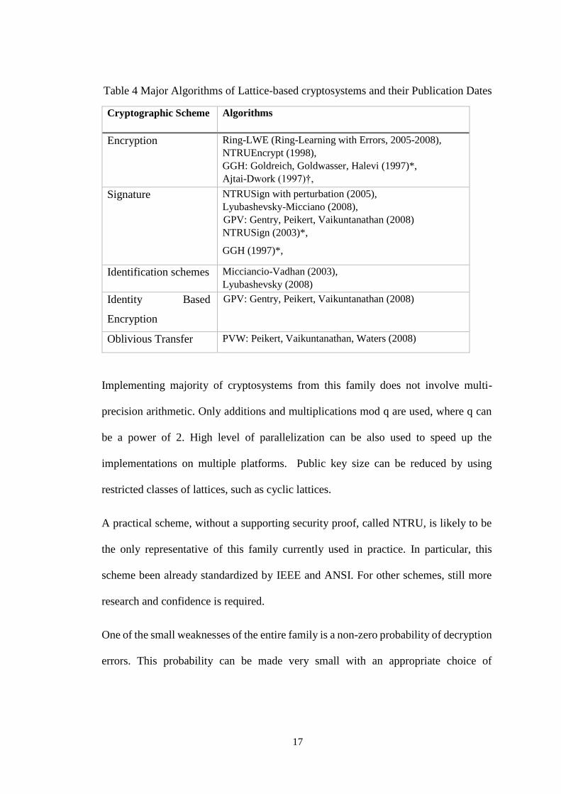
Table 4 Major Algorithms of Lattice-based cryptosystems and their Publication Dates
Cryptographic Scheme Algorithms
Encryption Ring-LWE (Ring-Learning with Errors, 2005-2008),
NTRUEncrypt (1998),
GGH: Goldreich, Goldwasser, Halevi (1997)*,
Ajtai-Dwork (1997)†,
Signature NTRUSign with perturbation (2005),
Lyubashevsky-Micciano (2008),
GPV: Gentry, Peikert, Vaikuntanathan (2008)
NTRUSign (2003)*,
GGH (1997)*,
Identification schemes Micciancio-Vadhan (2003),
Lyubashevsky (2008)
Identity Based
Encryption
GPV: Gentry, Peikert, Vaikuntanathan (2008)
Oblivious Transfer PVW: Peikert, Vaikuntanathan, Waters (2008)
Implementing majority of cryptosystems from this family does not involve multi-
precision arithmetic. Only additions and multiplications mod q are used, where q can
be a power of 2. High level of parallelization can be also used to speed up the
implementations on multiple platforms. Public key size can be reduced by using
restricted classes of lattices, such as cyclic lattices.
A practical scheme, without a supporting security proof, called NTRU, is likely to be
the only representative of this family currently used in practice. In particular, this
scheme been already standardized by IEEE and ANSI. For other schemes, still more
research and confidence is required.
One of the small weaknesses of the entire family is a non-zero probability of decryption
errors. This probability can be made very small with an appropriate choice of

18
parameters (e.g. 1%). Any encryption scheme can be also combined with error
correction codes to reduce error probability to undetectable levels.
Table 5. Public Key Sizes for Lattice-based algorithms for selected Security Levels.
112-bit 128-bit 192-bit 256-bit
NTRU: 552 B
(N=401, q=211)
[EBACS]
NTRU: 604 B
(N=439, q=211)
[EBACS];
LWE: 140 KB
NTRU: 815 B
(N=593, q=211)
[EBACS]
NTRU: 1022 B
(N=743, q=211)
[EBACS]
* 1 KB = 1024 bytes
† NTRU: public key size = N·log2 q
2.1.3 NTRUEncrypt Cryptosystem
NTRUEncrypt is a polynomial ring-based public-key encryption scheme that was first
introduced at Crypto’96. The first formal paper describing this scheme was published
at ANTS III [13]. In 2008, an extended version of this algorithm was published as the
IEEE 1363.1 Standard Specification for Public Key Cryptographic Techniques Based
on Hard Problems over Lattices [14]. Within the standard, the described algorithm is
called Short Vector Encryption Scheme – SVES. Since the core of this algorithm is
known in the academic literature as NTRUEncrypt, we will refer to the full
cryptosystem as NTRUEncrypt SVES. Further standardization efforts included the
Financial Services Industry Standard ANSI X9.98-2010 [15] and the Consortium for
Efficient Embedded Security standard, EESS #1 [16]. Additionally, an Internet Draft
proposing the use of NTRUEncrypt in the handshake for the Transport Layer Security
(TLS) v1.3 has been developed in 2016 [17].

19
The recent renewed interest in NTRU is at least partially driven by its presumed
resistance to any efficient attacks using quantum computers. In Feb. 2016, NIST has
published a draft report [18] and announced its plans of starting the standardization
effort in the area of post-quantum cryptography [19]. This effort is likely to last years
and result in an entire portfolio of algorithms capable of replacing current public-key
cryptography schemes. This initial announcement was followed by the official Call for
Proposals and Request for Nominations for Public-Key Post-Quantum Cryptographic
Algorithms, issued in Dec. 2016 [20]. As a part of this standardization process, fair and
efficient benchmarking of PQC algorithms in hardware and software becomes a
necessity.
NTRUEncrypt has three major parameters (N, p, q) such that
a) N is prime,
b) p and q are relatively prime, gcd(p,q)=1, and
c) q is much larger than p
For the purpose of efficiency p is typically chosen to be 3, and q as a power of two. The
scheme is based on polynomial additions and multiplications in the ring R=Z[X]/XN-1.
We use the “∗” to denote a polynomial multiplication in R, which is the cyclic
convolution of the coefficients of two polynomials. After completion of a polynomial
multiplication or addition, the coefficients of the resulting polynomial need to be
reduced either modulo q or p. The key creation process also requires two polynomial
inversions, which can be computed using the Extended Euclidean Algorithm. During
the key generation, the user chooses two random secret polynomials F ∈ R and g ∈
R, with so called “small” coefficients, i.e., coefficients reduced modulo p (typically
20
chosen to be in the integer range from -1 to +1, and thus limited to -1, 0, and 1. The
private key f is computed as f=1+pF. The public key h is calculated as
h = f-1 * g p in (Z/qZ)[X]/(XN – 1)
The message m is assumed to be a polynomial with “small” coefficients. The ciphertext
is computed as
e = r * h + m (mod q)
where r ∈ R is a randomly chosen polynomial with “small” coefficients.
The decryption procedure requires the following three steps:
1) calculate f ∗ e (mod q)
2) shift coefficients of the obtained polynomial to the range [−q/2, q/2),
3) reduce the obtained coefficients mod p.
2.2 Technology
2.2.1 Hardware/Software Codesign Platforms
In this section, we will provide information on alternative HW/ SW codesign platforms
other than Zynq SoC.
1. Discrete FPGA-Processor Combination: In this scenario, processor and
FPGA exist as physical separate components. The major disadvantage of this
platform is the huge overhead of inter-chip communication.
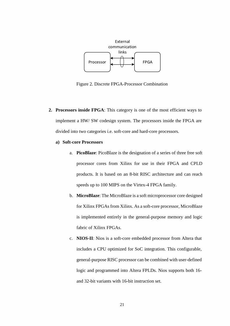
21
Processor FPGA
External communication
links
Figure 2. Discrete FPGA-Processor Combination
2. Processors inside FPGA: This category is one of the most efficient ways to
implement a HW/ SW codesign system. The processors inside the FPGA are
divided into two categories i.e. soft-core and hard-core processors.
a) Soft-core Processors
a. PicoBlaze: PicoBlaze is the designation of a series of three free soft
processor cores from Xilinx for use in their FPGA and CPLD
products. It is based on an 8-bit RISC architecture and can reach
speeds up to 100 MIPS on the Virtex-4 FPGA family.
b. MicroBlaze: The MicroBlaze is a soft microprocessor core designed
for Xilinx FPGAs from Xilinx. As a soft-core processor, MicroBlaze
is implemented entirely in the general-purpose memory and logic
fabric of Xilinx FPGAs.
c. NIOS-II: Nios is a soft-core embedded processor from Altera that
includes a CPU optimized for SoC integration. This configurable,
general-purpose RISC processor can be combined with user-defined
logic and programmed into Altera FPLDs. Nios supports both 16-
and 32-bit variants with 16-bit instruction set.

22
d. OpenSparc: OpenSPARC is an open-source hardware project
started in December 2005. The initial contribution to the project was
Sun Microsystems' register-transfer level (RTL) Verilog code for a
full 64-bit, 32-thread microprocessor, the UltraSPARC T1
processor.
e. LEON3: The LEON3 is a synthesizable VHDL model of a 32-bit
processor compliant with the SPARC V8 architecture. The full
source code is available under the GNU GPL license, allowing free
and unlimited use for research and education.
f. Dalton 8051: The Intel 8051 is an 8-bit micro-controller. This
micro-controller is capable of addressing 64K of program and 64K
of data memory. The implementation is written in Synthesizable
VHDL and models the actual Intel implementation rather closely,
e.g., it is 100% instruction compatible.
g. ARM Cortex-M1: The ARM Cortex-M1 processor is the first ARM
processor designed specifically for implementation in FPGAs. The
Cortex-M1 processor targets all major FPGA devices. The Cortex-
M1 processor enables cost savings through rationalization of
software and tools investments across multiple projects spanning
FPGA, ASIC and ASSP, plus greater independence through use of
an industry-standard processor.
b) Hard-core Processors: These processors are permanently embedded at
fixed location inside FPGA but have an advantage that they can run at a
much higher frequency and provide performance benefits.
23
a. IBM PowerPC: The single hard processor to be discussed is the
IBM PowerPC, which was included as a hard processor in the
Virtex-II Pro and subsequently in a subset of Virtex-4 and Virtex-5
FPGAs. Each of these FPGAs includes either one or two PowerPC
(PPC) units.
b. ARM Cortex M3: This processor is available as a hardcore inside
Microsemi SmartFusion2 SoC: The ARM Cortex™-M3 32-bit
processor has been specifically developed to provide a high-
performance, low-cost platform for a broad range of applications,
including microcontrollers, automotive body systems, industrial
control systems and wireless networking. With a balance between
size and speed, Microsemi's free Cortex-M3 processor is included
as a hard resource in Microsemi's SmartFusion2 and SmartFusion
SoC FPGA families.
c. ARM Cortex A9: This dual core processor is available in Altera
Cyclone V, Arria V, Arria 10 and Cyclone V FPGAs and provides
the equivalent performance as Zynq SoC 7020 EPP platform.
2.2.2 Hardware/Software Codesign with Xilinx Zynq SoC
In this section, we will discuss all building blocks required to construct HW/ SW
codesign using Zynq SoC platform. It is critical to rationally decide about the
components of the codesign effort because later on, they have a huge impact on the
performance and area utilization of your overall design.

24
Platform
Typically, implementations are classified into software and hardware implementations.
There are very few high-speed implementations done using HW/SW codesign
approach. These available implementations largely suffer from low-performance
processors and communication overhead between the processor and hardware
accelerator. Having a processing system (PS) and programmable logic (PL) on a single
chip greatly reduces the delays between both parts. For an efficient system, it is
imperative to perform well in all areas, i.e., software, communication interface and
hardware side. Our design platform uses Xilinx Zynq SoC 7020 Extensible Processing
Platform (EPP). This chip is specifically designed for HW/SW cosdesign applications
in mind and optimizes the design in all three domains of a codesign system.
Processing System (PS)
Zynq SoC platform provides dual core ARM Cortex-A9 microprocessor core with
CPU frequency up to 1 GHz. Zynq has 32 KB of L1 data and instructions caches,
512 KB of L2 cache and 512 MB DDR3 memory. This ensures high speed
implementation of the software side of the design.

25
S_AXI_LITE
S_AXIS_S2MMM_AXI_MM2S
AXI Direct Memory Access
M_AXI_S2MM
M_AXIS_MM2S
AXI Timer
S_AXI
S00_AXI
S00_AXISM00_AXIS
FPGA Coprocesor
S00_AXI
S01_AXIM00_AXI
AXI Interconnect
S_AXI_ACP
ZYNQ7 Processing System
M_AXI_GP0DDR
FIXED_IO
S00_AXI M00_AXI
M01_AXIM02_AXI
AXI Interconnect
Figure 3. Zync SoC Z7020 platform with interface between PS and PL
Programmable System (PL)
Zynq SOC platform provides a reconfigurable logic equivalent to Artix-7 FPGA. It
consists of 85K Logic cells (Slices). Additionally, it offers embedded resources i.e. 140
BRAMs (36kbit each) and 220 DSP blocks.
Serial in Parallel out (SIPO) and Parallel in Serial out (PISO) Components:
SIPO and PISO components are a part of input and output interface. SIPO takes in “n”
w-bit wide data words serially and convert them into one b-bit wide output word that is
n*w-bit wide. On the other hand, PISO takes in parallel input (b = n*w-bit wide) and
converts it w-bit words that is serially transmitted out.
26
en rst
dout
w
Reg
w
en rst
w
Reg
w
b
en rst
w
Reg
w
en rst
w
Reg
w
din
Figure 4. SIPO in Input interface of Coprocessor
01
w w
01
w w
01
w w
din
dout
en rst
w
Reg
w
en rst
w
Reg
w
en rst
w
Reg
w
en rst
w
Reg
w
selsel sel
b
Figure 5. PISO in Output interface of Coprocessor
Choice of Processor (PS) Ports for Communications
There are three major types of PS ports available for communication with PL using
AXI interface.
General Purpose (GP) port
In GP interface, coprocessor acts as a slave. It attaches the coprocessor to a general
purpose coprocessor port on the PS. Here, coprocessor is considered as a register
interface with a memory mapped address. This is the simplest way of attaching the
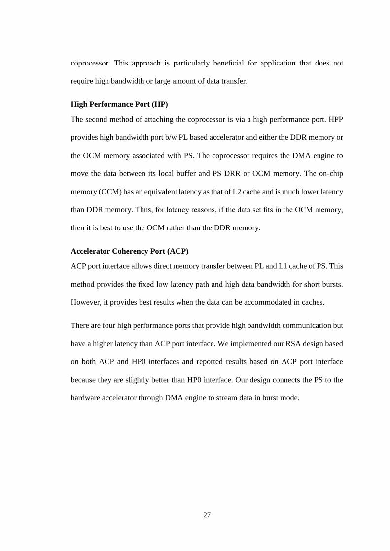
27
coprocessor. This approach is particularly beneficial for application that does not
require high bandwidth or large amount of data transfer.
High Performance Port (HP)
The second method of attaching the coprocessor is via a high performance port. HPP
provides high bandwidth port b/w PL based accelerator and either the DDR memory or
the OCM memory associated with PS. The coprocessor requires the DMA engine to
move the data between its local buffer and PS DRR or OCM memory. The on-chip
memory (OCM) has an equivalent latency as that of L2 cache and is much lower latency
than DDR memory. Thus, for latency reasons, if the data set fits in the OCM memory,
then it is best to use the OCM rather than the DDR memory.
Accelerator Coherency Port (ACP)
ACP port interface allows direct memory transfer between PL and L1 cache of PS. This
method provides the fixed low latency path and high data bandwidth for short bursts.
However, it provides best results when the data can be accommodated in caches.
There are four high performance ports that provide high bandwidth communication but
have a higher latency than ACP port interface. We implemented our RSA design based
on both ACP and HP0 interfaces and reported results based on ACP port interface
because they are slightly better than HP0 interface. Our design connects the PS to the
hardware accelerator through DMA engine to stream data in burst mode.
28
Figure 6. Processor Ports for Communication between PS and PL
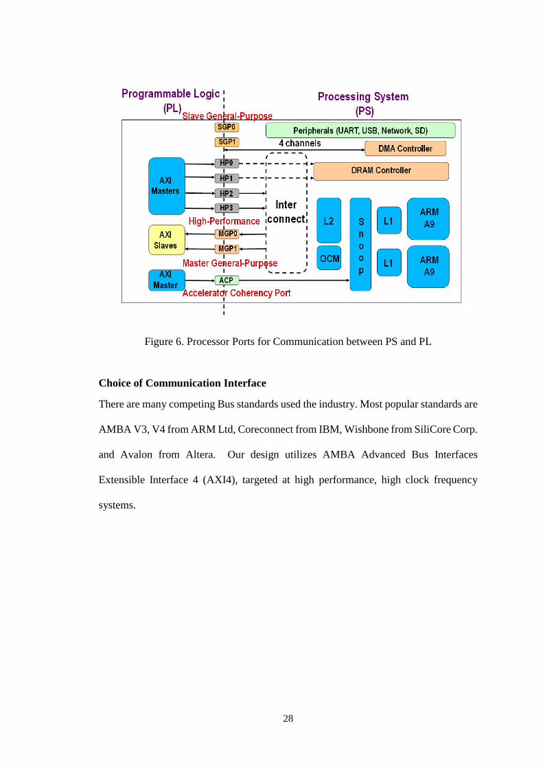
Choice of Communication Interface
There are many competing Bus standards used the industry. Most popular standards are
AMBA V3, V4 from ARM Ltd, Coreconnect from IBM, Wishbone from SiliCore Corp.
and Avalon from Altera. Our design utilizes AMBA Advanced Bus Interfaces
Extensible Interface 4 (AXI4), targeted at high performance, high clock frequency
systems.

29
Table 6. Communication Interface Options in Zync SoC
Bus configurations for existing bus standards
Bus
High-performance
shared bus
Peripheral
shared bus
Point-to-point
bus
AMBA v3 AAHB APB
AMBA v4 AXI4 AXI4-Lite AXI-Stream
Coreconnect PLB OPB
Wishbone Crossbar topology Shared topology
Point to point
topology
Avalon Avalon-MM Avalon-MM Avalon-ST
2.2.3 Type of AXI Interfaces in Zynq SoC
AXI is a part of ARM’s AMBA bus. Zynq SoC platform provides either a memory
mapped or stream interface to connect PS to PL.
AXI Interfaces
Memory Mapped
(Shared Bus)
Stream
(Point-to-Point
Bus)
Full AXI
(Burst Capable)
(High Performance)
AXI-Lite
(Single-beat)
(Peripheral)
Figure 7. AXI Interfaces

30
AXI4-Lite Interface
AXI4-Lite interface is a part of memory mapped interface with no burst capability. This
interface is generally used to connect peripheral that have low performance
requirement.
AXI Full Interface
AXI Full is the memory mapped interface that allows you to have the burst capability
and is typically used for high performance peripherals.
Address
and
Control
Read Data Channel
Write Data Channel
Write Address Channel
Write Response Channel
Ma
ste
r
Slav
e
Read
data
Read address channel
Address
and
Control
Ma
ste
r
Slav
eWrite
data
Write address channel
Read data channel
Write data channel
Write
response
Write response channel
Read Address Channel
Figure 8. AXI-Lite Interface
31
Address
and
Control
Read Data Channel
Write Data Channel
Write Address Channel
Write Response Channel
Ma
ste
r
Slav
e
Read
data
Read address channel
Read
data
Read
data
Address
and
Control
Ma
ste
r
Slav
eWrite
data
Write address channel
Read data channel
Write data channel
Write
dataWrite
data
Write
response
Write response channel
Read Address Channel
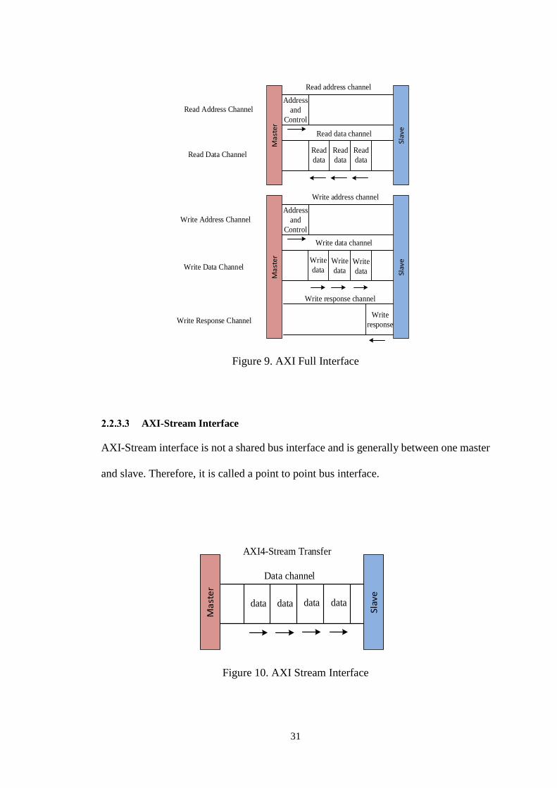
Figure 9. AXI Full Interface
AXI-Stream Interface
AXI-Stream interface is not a shared bus interface and is generally between one master
and slave. Therefore, it is called a point to point bus interface.
Ma
ste
r
Slav
e
data
AXI4-Stream Transfer
Data channel
data data data
Figure 10. AXI Stream Interface

32
2.2.4 AXI DMA
The coprocessor requires DMA transfer to move the data between its local buffer and
the L1/ L2 data caches. Once the data is ready for processing, A9 processor signals the
coprocessor via the slave port that it may begin processing the data. The communication
includes the address of the data. The coprocessor initiates a DMA transfer from the
memory, in this case, the L1/ L2 cache to its local buffer. The coprocessor processes
the data and returns the results in the 2nd buffer. The coprocessor initiates a DMA
transfer from the buffer to the memory, L1/L2 cache. Finally the coprocessor signals
the A9 processor that the data processing has been complete. The processor may then
use the data passed to it.
2.2.5 Embedded FPGA Resources
Practically all FPGA vendors incorporate in modern FPGAs, apart from basic
reconfigurable logic resources, also embedded resources, such as large memory blocks,
DSP units, microprocessors, etc. Improved hardware performance and good balance in
terms of the overall FPGA utilization can be achieved with the use of these embedded
elements for multiple applications, such communications, digital signal processing, and
scientific computing.
DSP Units
Xilinx Virtex 5 FPGAs include DSP48E units. Each unit has a two-input multiplier
followed by multiplexers and a three-input adder/subtractor/accumulator. The unit can
be configured as a 25x18 multiplier and/or 48-bit adder with up to three inputs. The
third input of an adder can be used only when multiple DSP units are cascaded and an
adder output of one DSP unit is connected to an adder input of an adjacent DSP unit.

33
The DSP unit of the Stratix III FPGAs consists of four subunits units (called DSP_18s)
and a total of eight 18x18-bit multipliers. Two neighboring 18x18 multipliers share a
37-bit adder. The outputs of two 37-bit adders are fed to second stage
Adder/Accumulator. Xilinx Spartan 3 and Altera Cyclone II contain only embedded
multipliers. Spartan 3 devices support 18x18 signed multiplication. Cyclone II devices
support 9x9 and 18x18 multiplication for signed and unsigned numbers.
Figure 11. DSP48 inside Zync SoC Z7020 and Latency selection to operate at 400
MHz
34
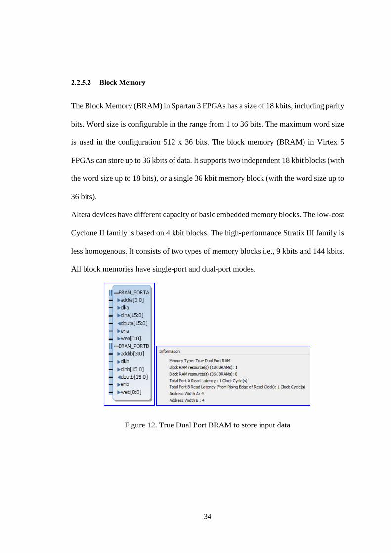
Block Memory
The Block Memory (BRAM) in Spartan 3 FPGAs has a size of 18 kbits, including parity
bits. Word size is configurable in the range from 1 to 36 bits. The maximum word size
is used in the configuration 512 x 36 bits. The block memory (BRAM) in Virtex 5
FPGAs can store up to 36 kbits of data. It supports two independent 18 kbit blocks (with
the word size up to 18 bits), or a single 36 kbit memory block (with the word size up to
36 bits).
Altera devices have different capacity of basic embedded memory blocks. The low-cost
Cyclone II family is based on 4 kbit blocks. The high-performance Stratix III family is
less homogenous. It consists of two types of memory blocks i.e., 9 kbits and 144 kbits.
All block memories have single-port and dual-port modes.
Figure 12. True Dual Port BRAM to store input data

35
Cryptographic algorithms have been demonstrated in the past to take advantage of these
resources as well. For example, the fastest to date FPGA implementation of the
Montgomery multiplication, a major building block of public key cryptographic
algorithms, such as RSA, have been demonstrated using DSP units in Virtex 5 FPGAs
[21].

36
3 SURVEY OF PREVIOUS WORK
The gap between performance and flexibility can be narrowed down through an
efficient HW/ SW codesign system. To develop such an environment, all aspects of
software, hardware and interface between the software and hardware for
communication should be taken care of. HW/SW co-design allows the designer to
partition the design into hardware and software to aim for the best of both worlds. The
flexibility and short development time of software is combined with performance and
low-power/low energy consumption of hardware.
This chapter covers the previous work on HW/SW implementations of RSA, currently
available implementations of Lattice based cryptosystems, existing coprocessor designs
on RSA/ ECC and HW/ SW codesign platforms that are already used by researchers.
3.1 HW/ SW Codesign Implementations of RSA
Public-key cryptosystems such as RSA have been widely used to secure digital data in
many commercial systems. Modular arithmetic on large operands used during modular
exponentiation makes RSA computationally challenging. We highlight some of the
attempts made to optimize RSA cryptosystem through HW/SW codesign.
Two variants of hardware/software co-design were presented by Simka et al. in [24]
where they utilize one Montgomery multiplier (MM) coprocessor and two pipelined
MM coprocessors respectively. The later implementation was aimed towards
minimizing the average execution time during decryption in RSA. They used
Altera’s Nios RISC processor as their building block. Their data path is organized
as a cascade chain of processing elements implemented using two approaches for
37
MMM operations to target scalability, i.e., carry save adder based and carry propagate
adder based MMM units. The word length, number of words, and number of stages can
be changed according to the required area of the implemented coprocessor and the
required timings for MM computations or the security level for flexibility of the
coprocessor.
Hani et al. in [25], proposed a private and public key cryptoprocessor. For RSA, the
entire ME is performed in hardware. However they do not employ any techniques to
make the design scalable by allowing different operand sizes or flexible by modular
exponentiation algorithms and multiple security levels.
Isaad et al. in [26] proposed two implementations for HW/SW co-design based on
right-to-left (R2L) algorithm for modular exponentiation. They propose a relatively
flexible architecture for modular exponentiation (ME) using three implementation
approaches, i.e SW only, with one MMM unit working sequentially, and two MMM
units used in parallel to perform a ME. The second variant utilizes only one modular
multiplier within a custom hardware. The execution time is further improved by
parallel implementation of two multipliers based on Montgomery algorithm as their
custom IP. The control of ME was done through MicroBlaze. Some data transfers are
also handled by local memories to reduce data transfer overhead. The highest level of
operation in all three schemes was MMM. However, in their proposed designs, the
scalability of modular multiplier is achieved by allowing different operand sizes,
modular exponentiation algorithms, or multiple security levels.
The implementations with the highest level operation being MMM offer higher
flexibility but lower performance as compared to the other approach, i.e., to implement

38
ME in hardware. To explore the best tradeoff between performance and flexibility, we
intend to focus on multiple aspects. One of them is to allow support of multiple
exponentiation algorithms i.e., R2L, L2R, sliding window. For highr flexibilility,
handling of multiple operand sizes in the MMM unit, the capability to control the choice
of ME algorithm form the software will be exploited.
The table below lists all noteworthy contributions on HW/SW codesign of RSA. The
security level in all reported implementations is equivalent to 80-bit security. Except
[26], all reported implementations use Left-to-Right algorithm for exponentiation.
Table 7. HW/ SW Codesign Implementations of RSA
Note: In the Flexibility/Scalability column, the parameters marked with * are used for the
reported results
1 Montgomery Powering Ladder, 2 Blinded Fault Resistant Exponentiation, 3 Highest level of operation implemented in
hardware is ME
Source Flexibility/
Scalability
Platform Area[LUTs/
LEs/Kgates,
RAMs,
DSP48]
Clk
Freq
MHz
Time
[ms] Device Processor
Isaad,
2014 [26]
1 MM unit in HW, 2
MM units in
hardware*, ME
scheme: R2L/ Fixed
operand size: 1024-bit
Xilinx
Virtex-5 MicroBlaze 1848, 11, 22 62.5 22.25
Uhsadel,
20123 [27]
Multiple ME schemes:
L2R*, R2L, MPL1,
BFR2/ Fixed operand
size: 1024-bit
Xilinx
Virtex-4,
XC4VFX101
8051 27467, 0, 1 111 29.37
Sakiyama,
2007 [6]
ME scheme: only
binary-method/ Fixed
operand size:1024-bit
Virtex-II
PRO,
XC2VP30
8051 49.5 Kgates,
6, 0 12 129.8
Hani,
2006 [25]
No Flexibility/ Fixed
operand size: 1024-bit EPLS40 NIOS
12881 LEs,
0,0 66 31.9
Simka,
2003 [24]
1 MM unit in HW, 2
MM units in
hardware*/ Operand
size: 1024*, 2048
Altera
APEX,
EP20K200E
FC484-2X
NIOS 2837 LEs,
N/A, 0 50 39
39
3.2 Previous HW/ SW Codesign Implementations on Traditional
Public-Key Cryptography
The scope of this research is to develop a HW/ SW codesign that offers the advantages
of flexibility in software but also offers the performance comparable to hardware. An
optimal HW/SW codesign is possible only if the designer looks at overall system-level
integration. In this section, we will look at the existing coprocessor implementations in
the field of public key cryptosystems that try to solve the underlying challenges of
HW/SW codesign approach.
Typically, papers on public-key cryptography are categorized into low area and high
speed implementations. Low area platforms include 8-bit microcontrollers (e.g. AVR
or 8051) [9], [4], [28], [10] as well as 32-bit microprocessors with bus systems (e.g
MSP430, ARM Cortex M0) [29] , [30], [31]. MicroBlaze with PLB and FSL bus and
ARM Cortex-A9 operates at a much higher frequency and they are considered suitable
for medium to high-speed implementations. In case, there is an additional requirement
for performance, the compute intensive of the algorithms are offloaded to
reconfigurable logic inside FPGA. These dedicated accelerators implemented inside
FPGA are typically called hardware coprocessors. As ECC provides equivalent security
to RSA with much smaller key sizes, it is more suitable for low-area and low-power
applications. Therefore, most of the earlier HW/SW implementations utilized smaller
processors (i.e. softcore processor like Dalton 8051, AVR, PicoBlaze, MicroBlaze)
along with FPGA reconfigurable resources for time consuming tasks. We will provide
details of previous HW/ SW implementations of ECC in this section that focused on
overall system-level design approach and optimized their designs for flexibility and
scalability.

40
Table 8. HW/ SW Codesign Implementations of ECC for 80-bit security.
Note: In the Flexibility/Scalability column, the parameters marked with * are used for
the reported results
Source Flexibility/
Scalabilty
Highest Level
Operation in
Hardware
Platform Area
[LUTs/
LEs,
RAMs,
DSP48]
Clk
Freq.
[MHz]
Time
[ms] Device Processor
Balasch,
2014 [32]
Fixed curve /Fixed
operand size =
256-bit
Scalar
Multiplication
Virtex-5,
XC5VLX30
-2FF324
8051 2525, 6, 27 39.4 10.6
Hassan,
2010 [33]
Supports 5 NIST
curves (m =163*,
233, 283 409,
571)/ Supported
datapath widths =
8, 16, 32-bit*
Binary Field
Modular
Multiplication
Spartan-3,
XC3S200
32-bit
PicoBlaze 1127, 4, 0 68.3 380
Sakiyama,
2006 [6]
Fixed curve /Fixed
operand size =
160-bit
Montgomery
Modular
Multiplication,
Modular
Add/Subtract
Virtex-II
PRO
XC2VP30
8051 49.5 Kgates,
6, 0 12 129.8
Koschuch
2006 [28]
Two Operand
sizes = 163*, 191-
bit
Binary Field
Modular
Multiplication
N/A 8051
(Dalton)
29.4 Kgates,
0, 0 12 99
Batina,
2005 [10]
Fixed curve /Fixed
operand size =
160-bit
Modular
Multiplication,
Addition and
Inversion
N/A 8051
(Dalton) 3781, 0, 0 12 2488
Kumar,
2004 [4]
Fixed curve /Fixed
operand size =
160-bit
Binary Field
Modular
Multiplication
Atmel,
ATSTK94
FPSLIC
AVR 8-
bit MCU 498, 0, 0 4 113
One of the important steps to codesign efficiently is to explore the design space and
partition the design effectively. Some partition options are more suitable for high-speed,
while others offer more flexibility. In case of ECC, one way to partition is to assign full
point addition/ doubling operation to hardware and the remaining parts to software.
While this approach is very fast (there are no operand transfers during point addition/
doubling), it suffers from a relatively high hardware cost.
41
A second way to draw a line between hardware and software is to offload the field
arithmetic operations from the host processor and execute them in a dedicated hardware
accelerator, serving as a coprocessor. All other operations, i.e. point addition/ doubling
and scalar multiplication, are implemented in software and executed on the host
processor. In general, this approach offers high flexibility. On the other hand, it may
entail a significant communication overhead, especially when the coprocessor does not
provide local storage for the intermediate results.
Finally, the boundary between hardware and software can also be defined at the level
of custom instructions that are specifically designed to accelerate the field arithmetic,
most notably the field multiplication. HW/ SW codesign, at the granularity of
instruction set extensions provides the highest flexibility and requires the least amount
of extra hardware. However, these custom instructions are processor dependent. Each
processor instruction can take multiple clock cycles to execute. Also, the fundamental
bottlenecks of a sequential processor (memory access, sequential execution of code)
are also fundamental bottlenecks for an instruction set extension based design.
All designs except [32] and [6] present designs for binary fields. Kumar et al. [4]
presented an extremely low-cost implementation with instruction set extension using
reconfigurable logic, which enables an 8-bit microcontroller to provide full size elliptic
curve cryptography (ECC) capabilities. Their design was flexible due to the use of ISE
based processor, but worked on fixed curve and operand size of 160-bits only. Batina
et al. in [10] proposed a hardware/software co-design of the HECC system that was
implemented on a low-cost platform, an 8-bit 8051 microprocessor and utilized a small
42
hardware co-processor for field multiplication. This design was also inflexible in terms
of fixed curve and operand size.
Koschuch [28] proposed a HW/ SW codesign for ECC that supported two operand sizes
(163 and 191-bit). They also demonstrated the importance of removing system-level
performance bottlenecks caused by the transfer of operands between hardware
accelerator and external RAM by integrating a small direct memory access (DMA) unit.
Sakiyama et al. [6] presented a scalable architecture for accelerating public-key
cryptography. They developed a coprocessor for both ECC and RSA. The hardware
coprocessor had a modular arithmetic logic unit that was scalable and was able to work
on variable digit size (d). Although, they mentioned that the software code could be
made flexible to support multiple schemes (e.g. sliding window method, windowed
NAF, or signed m-ary), the design was able to work only with binary-method for point
multiplication.
Hassan et al. [33] developed a low-area scalable design that supported 5 different NIST
curves and variable data widths of 8, 16 and 32-bits. He performed binary field modular
multiplication in hardware coprocessor to make the design flexible and handle higher
level operations in software.
Balasch et al. [32] implemented several versions of coprocessors to explore the design
space for scalar multiplication. First coprocessor supported field multiplication, second
one supported field arithmetic (addition, subtraction and multiplication), third one
supported point arithmetic (point doubling, point addition) and fourth one supported
scalar multiplication. However, their design worked on fixed operand sizes and has no
provision to apply different multiplication schemes from the software.

43
Based on the previous work shown in this section, it is evident that all the HW/ SW
codesign implementations tried to achieve some sort of flexibility in their design. Apart
from one, all the designs tried to implement finite field multiplication in hardware
coprocessor in order to make their design more flexible. Very few designs provided a
support for multiple security levels. To the best of our knowledge, there were no designs
that provided support for different multiplication schemes controlled from the software
side and support for different operand sizes in one implementation. Thus, leaving room
for more investigation to provide highly flexible and efficient designs.
3.3 Previous Implementations of Lattice Based Cryptosystems
In this section, we will provide details about already published work by other
researchers in the area of Lattice based cryptography. We chose to investigate work on
encryption schemes of NTRU and Ring-LWE algorithms. Work on signature and
identification scheme, identity based encryption (IBE) and oblivious transfer are
beyond the scope of this research.
3.3.1 Previous Implementations of NTRU Cryptosystem
The software implementation of encryption schemes of NTRU are available in eBACS
(ECRYPT Benchmarking of Asymmetric Systems). These submitted implementations
can perform public-key encryption with 112, 128, 192, 256-bit equivalent security.
Bailey et al. [34] implemented NTRU on a wide variety of constrained devices,
including the Palm Computing Platform, Advanced RISC Machines ARM7TDMI, the
Research in Motion Pager, and finally, the Xilinx Virtex 1000 family of FPGAs.
O’Rourke et al. [35] presented a scalable architecture to perform NTRU
multiplication and also proposed a unified architecture based on Montgomery

44
multiplication. Kaps et al. [36] proposed a scalable low power design for the NTRU
polynomial multiplications. The smallest version of their design implemented only a
single arithmetic unit but the design was flexible to scale up the number of parallel
arithmetic units relatively easily with minimal impact on the other elements of the
design. In contrast to previous research, Atici et al. [37] presented a compact and low
power NTRU design that was suitable for pervasive security applications such as
RFIDs and sensor nodes. It was the first implementation to provide both encryption
and decryption in a single design. However, they targeted one parameter set to
implement fixed security level. Kamal et al. [38] investigated several hardware
implementation options for the NTRU encryption algorithm. In particular, by utilizing
the statistical properties of the distance between the non-zero elements in the
polynomials involved in the encryption and decryption operations, they presented an
architecture that offers different area-speed trade-off and analyzed its performance
on Virtex-E FPGA chip. The design was configurable to perform modular reduction
using Mersenne Prime based and LUT based architectures.
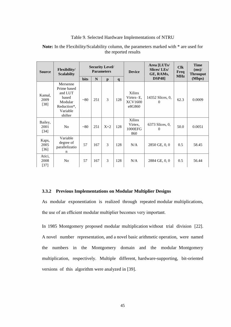
45
Table 9. Selected Hardware Implementations of NTRU
Note: In the Flexibility/Scalability column, the parameters marked with * are used for
the reported results
3.3.2 Previous Implementations on Modular Multiplier Designs
As modular exponentiation is realized through repeated modular multiplications,
the use of an efficient modular multiplier becomes very important.
In 1985 Montgomery proposed modular multiplication without trial division [22].
A novel number representation, and a novel basic arithmetic operation, were named
the numbers in the Montgomery domain and the modular Montgomery
multiplication, respectively. Multiple different, hardware-supporting, bit-oriented
versions of this algorithm were analyzed in [39].
Source Flexibility/
Scalabilty
Security Level/
Parameters Device
Area [LUTs/
Slices/ LEs/
GE, RAMs,
DSP48]
Clk
Freq
MHz
Time
(ms)/
Throuput
(Mbps) bits N p q
Kamal,
2009
[38]
Mersenne
Prime based
and LUT
based
Modular
Reduction*,
Variable
shifter
~80 251 3 128
Xilinx
Virtex- E,
XCV1600
e8G860
14352 Slices, 0,
0 62.3 0.0009
Bailey,
2001
[34]
No ~80 251 X+2 128
Xilinx
Virtex,
1000EFG
860
6373 Slices, 0,
0 50.0 0.0051
Kaps,
2005
[36]
Variable
degree of
parallelizatio
n
57 167 3 128 N/A 2850 GE, 0, 0 0.5 58.45
Atici,
2008
[37]
No 57 167 3 128 N/A 2884 GE, 0, 0 0.5 56.44

46
Tenca et al. [40] proposed the very first scalable architecture for Montgomery
Multiplication. Harris et al. in [41], and later on Huang et al. in [42] have improved this
design in terms of latency and latency*area by factor of two. Further improvement of
the aforementioned architectures was possible when radix-4 architectures were
introduced. They were demonstrated for the Tenca et al., Harris et al. and Huang et al.
designs in [43], [41] and [42], respectively.
Bipartite multiplication algorithm proposed in [44] enables a two-way parallelism by
using two custom modular multipliers. By combining a classical modular multiplication
based on Barret with Montgomery’s modular multiplication, it splits the operand
multiplier into two parts and processes them in parallel, increasing the calculation
speed. Later in [45], the proposed tripartite algorithm minimizes the number of single-
precision multiplications and enables more than 3-way parallel computation. It achieves
a higher speed compared to the bipartite algorithm. The algorithm is suitable for the
multicore parallelism.
Suzuki in [21] combined the Multiple Word Radix-2 Montgomery Multiplication
(MWR2MM) together with the quotient pipelining technique and proposed an
architecture which can be mapped efficiently onto a modern high-performance DSP-
oriented FPGA structure. Hardware architectures of modular arithmetic for parallel
computing were demonstrated using residue number system in [46] and spectral
modular arithmetic in [9] and [47].
We employ a Montgomery multiplication algorithm based on quotient pipelining
technique developed by Orup in 1991 [23]. The major differences between Orup's
Montgomery multiplication and classical Montgomery multiplication are discussed in
the background section.

47
4 HARDWARE/SOFTWARE CODESIGN OF RSA
Considering all the technological advancements and existing implementations of RSA,
we think it is realistic to improve the applicability of RSA for modern embedded
systems even further. In this chapter, we present a study of RSA implemented through
hardware/software codesign using Xilinx Zynq-7000 SoC platform. The originality of
our work lies in exploring the best trade-off between achieving maximum flexibility
from software, with an improvement in performance from hardware by balancing the
partitioning between hardware and software components of the design.
This chapter focuses on important design decisions to develop HW/ SW codesign
implementation of public key cryptosystems. RSA also serves as a case study to
describe the design process of a generic codesign methodology. The same approach
will be carried forward to build a HW/ SW codesign for Lattice based cryptosystems
(i.e., NTRU).
4.1 Software Development
4.1.1 Developing and Extending Software APIs in RELIC Library
Our software implementation is based on RELIC toolkit [48]. One of the major reasons
was to generate test vectors and intermediate results for functional verification of our
coprocessor implemented in hardware for RSA implementation. We have utilized the
already existing code base for modular exponentiation in RELIC for RSA
implementation.

48
4.1.2 Hardware/Software Partitioning
Profiling in one of the important feature of Zynq SoC software development kit (SDK).
Profiling can be helpful to fully understand the time critical operations of any design.
We used the built-in profiler provided as a part of Vivado Design Suite 2015.4 to
determine the compute intensive portions of RSA that take majority of the time in its
software implementation. Proper partitioning to find an optimum boundary between
software and hardware requires detailed know-how of the design and some level of
expertise. The profiler showed approximately 82% contribution of the Modular
Exponentiation (ME). In all the methods used to perform ME, there are repeated
modular multiplications at the lower level. The results generated because of profiling
were used to define boundaries between software and hardware well in advance.
RSA
Exponentiation
Modular Arithmetic
Software
in C
Hardware
in RTL
RSA
Exponentiation
Modular ArithmeticHardware
in RTL
Partitioning Scheme:
Software/ Hardware Mix 1
Partitioning Scheme:
Software/ Hardware Mix 2
RSA
Exponentiation
Modular Arithmetic
Software
in C
Partitioning Scheme:
Software Only
RSA
Exponentiation
Modular Arithmetic
Hardware
in RTL
Partitioning Scheme:
Hardware Only
Software
in C
Figure 13. Hierarchy of Operations and Tentative Partitioning Schemes in RSA
49
The figure above shows the possible partitioning schemes for an RSA-based
implementation.
• Scheme 1: Offers full flexibility, but low performance.
• Scheme 2: Modular arithmetic is offloaded to the coprocessor for improved
performance. Multiple exponentiation schemes can be implemented from
software to offer flexibility.
• Scheme 3: The entire ME is implemented in the coprocessor for maximum
performance gain. However, the design is less balanced between software and
hardware.
• Scheme 4: Maximum performance gain possible with very limited flexibility.
Implementing the entire ME in hardware leans more towards performance optimization
as it is quite close to having an entire RTL-based design. However, we implement
partitioning scheme 2 as it leaves more room to achieve the balance between flexibility
through software and performance from the coprocessor.
4.2 Operation of the Processing System
Zynq SoC platform provides dual core ARM Cortex-A9 microprocessor core. Zynq has
32 KB of L1 data and instructions caches, 512 KB of L2 cache and 512 MB DDR3
memory. This ensures high speed implementation from the software side of the design.
Our software implementation is based on RELIC toolkit [48]. RELIC was developed in
Brazil as a part of the TinyPBC project and is optimized for embedded applications.

50
Table 10. Implemented hardware functions
Function Call Description
SET_OP_SIZE () To set operand size in PL using AXI-LITE interface
LW_M () Loads modulus from PS through AXI-STREAM
interface to the multiplier unit in PL
LW (Reg_Num, A) Loads data from PS through AXI-STREAM
interface to Reg_Num in local memory of PL
SW (A, Reg_Num) Stores data from Reg_Num in local memory of PL
through AXI-STREAM interface to PS
Hw_mul_monty_orup4 (dst, src1,
src2)
Sends a control word through AXI-LITE interface
to load operands from addresses src1 and src2 of the
local memory to perform multiplication. The result
is stored in address specified by dst.
To achieve the flexibility in our RSA design, exponentiation is performed in software.
This allows us to choose any of the exponentiation schemes, i.e., Left-to-Right (L2R),
Right-to-left (R2L) or Sliding window method from software.
Types of Exponentiation and Instruction Set:
For all three variants to perform ME, we implemented corresponding functions in
RELIC based on Montgomery multiplication using Orup's algorithm. In Algorithm 5,
line 17, the function bn_rec_slw() is a function in RELIC used to windows win[0],
win[1], ..., win[l-1]. Based on the windows, val[win[i]] is the index of the leftmost 1 in
the binary representation of win[i]. Once this function is called during pre-processing,
l becomes the number of windows rather than the number of bits in the exponent. The
same implementations were used to for functional verification of the hardware

51
implementation. Also, the conversion of operands to/from Montgomery domain can be
realized using Orup's Montgomery Product (OMP) in the coprocessor.
We present the instruction set in Table 10 along with the description of the operation
of all instructions. Next, we present all three ME schemes with function calls to the
hardware in algorithms 3, 4 and 5. In Algorithm 5, the additional step is the pre-
processing in which the RELIC based function bn_rec_slw() is executed. Post-
processing includes only one modular reduction in all three algorithms. In the
processing phase, we use the hardware API's to transfer data and control words to the
hardware coprocessor while performing modular multiplications.
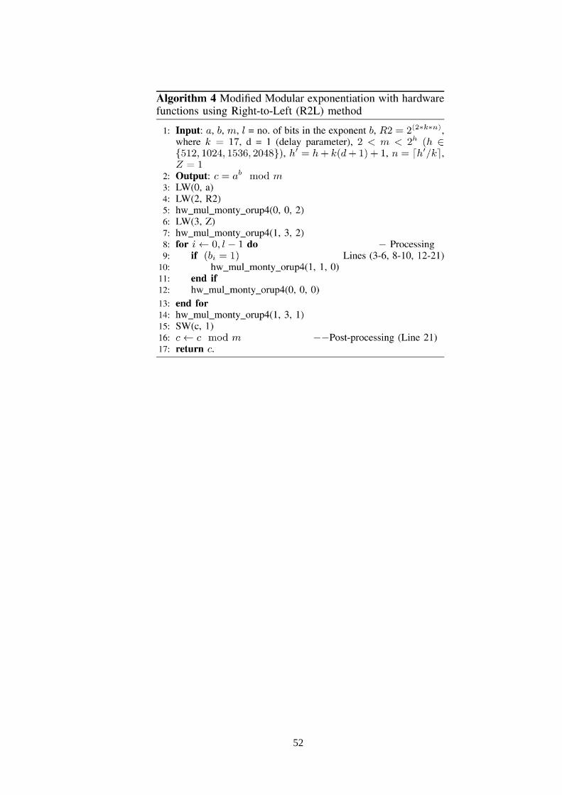
52

53
4.3 Choice of Communication Interface
There are many competing Bus standards used the industry. Most popular standards are
AMBA V3, V4 from ARM Ltd, Coreconnect from IBM, Wishbone from SiliCore Corp.
and Avalon from Altera. Our design utilizes AMBA Advanced Extensible Interface 4
(AXI4), targeted at high performance, high clock frequency systems. There are three
methods to attach a co-processor to the processing system (PS).
• Hardware accelerator attached as a general purpose port (GP0)
54
• Hardware accelerator attached via high performance port (HP0)
• Hardware accelerator attached using Accelerator Coherency Port (ACP)
ACP port interface allows direct memory transfer between PL and L1 cache of PS. This
method provides the fixed low latency path. However, it provides best results when the
data can be accommodated in caches. There are four high performance ports that
provide high bandwidth communication but have a higher latency than ACP port
interface. We implemented designs based on both ACP and HP0 interfaces and reported
results based on ACP port interface because they are slightly better than HP0 interface.
Our design connects the PS to the hardware accelerator through DMA engine to stream
data in burst mode. Hardware coprocessor receives input arguments from PS into the
local memory and sends them to the multiplier unit. Once modular multiplication is
completed, result is stored in the local memory while the system waits for the next
control word through AXI-Lite interface. When the entire exponentiation is performed,
the result is sent back to PS through AXI-Stream interface.
4.4 Implementing Programmable Logic (PL) – Our Hardware
Accelerator
Our design process of a hardware coprocessor is further categorized into the following
four major components
• Compute Kernel: Coprocessor unit to perform compute intensive tasks
• Controller: It includes the command interpreter, input FSM, compute FSM and
output FSM
• Interface: Interface with the bus that includes argument and result storage
• Local Memory: To store the intermediate results in hardware

55
Compute Kernel:
In our implementation, the compute kernel for RSA performs Montgomery modular
multiplication. Our design for the compute kernel is targeted towards achieving both
scalability and performance. The implementation is based on Orup's implementation
by Suzuki from [21]. We extended the basic Montgomery multiplier with an interface
for input and output. The datapath is scalable for multiple operand sizes, i.e., 512, 1536,
1024 and 2048 without any increase in the area. The command interpreter which is part
of the controller is used to send a control word with the information of operand size
from PS to PL. The operands are loaded into the local memory of the coprocessor at
the start of the operation through AXI-Stream interface. The operands are stored locally
into dual-port RAMs to reuse them and to minimize the overhead associated with data
transfer from PS to PL. DSP48E macros are used to multiply operands in radix 217.
Latency of these DSP units is adjusted to 3 to operate them at the maximum operating
frequency to achieve better performance.
Controller:
Our controller consists of the command interpreter, input FSM, output FSM and
compute FSM. Command interpreter acts as a bridge between software and hardware.
It receives commands words from PS through AXI-Lite interface, interprets them and
then distributes the control signals to the input, output and compute FSMs accordingly.
In a standard approach, operands are fed into the compute kernel, result is computed
and send back to PS. Our design is configurable to work with variable operand sizes
and different optimization schemes controlled from PS. This requires that the controller
56
can dynamically adopt and generate the control signals for input, compute and output
FSM.
BRAM
BRAM
VSL
VSR
ai or mi
Input Storage
2k
2k
AXI-Lite Interface
src2src1dstRR
REG0 REG1
Cmd/ Data
m
2 6 6 6
Input FSM
Cmd Status
Compute FSM
Cmd Status
Output FSM
Cmd Status
Command Interpreter
BRAM
BRAM
VSL
VSROut Stream
2k
2km
Compute Kernel
S_src10
mi
bi
S_src11
mi
S_src1k-1
mi
S2
In Stream
Controller
S_src20
S_src21
S_src216
S_src10
S_src20
S_src11
S_src21
S_src1k-1
S_src2k-1
2k
S2
Output Storage
2k
2k
2k
2k
2k
2k
2k
2k
2k
VSR: Variable Shift RightVSL: Variable Shift Leftm: 32-bit Busk: 17 (Words size)Dst: Destination address (Local Memory) Src1: Source 1 address (Local Memory)Src2: Source 2 address (Local Memory)
AX
I-St
ream
Inte
rfac
e AX
I-Stream
Interface
m
2k
2k
2k
2k
2k
2k
2k
2k
2k
2k
2k
2k
2k
2k
2k
2k
2k
2k
k
Figure 14. Detailed Hardware Coprocessor Design
57
I/O Interface:
Our I/O interface is implemented using dual port block memories to support width
conversion necessary for the compute kernel to process data. It also takes care of the
communication between PS and PL through synchronization signals and flags between
PS and PL. We use Accelerated coherency port (ACP) to stream data into PL. DMA
unit is used to handle communication in this scenario.
Local Memory:
Local memory provides local access to the intermediate results. Storing intermediate
results into one of the available memories (L1/ L2 caches, OCM and DDR3 memory)
associated with PS is very costly in terms of clock cycles. Each read/ write access to L1
and L2 caches costs 27 and 32 clock cycles respectively. Access to the L1/ L2 caches
is possible only if we use Accelerated Coherency Port (ACP). Similarly, accessing On-
Chip memory (OCM) and DDR3 memory cost 27 and 89 clock cycles respectively.
High Performance Ports (HP0-3) can only access the OCM and DDR3 memories using
46 and 76 clock cycles respectively. Using General Purpose Ports (GP0-3) has the
biggest penalty and takes 88 and 118 clock cycles to access OCM and DDR3 memories.
Using local memory implemented through dual-port block memories in FPGAs, on the
other hand, only requires few clock cycles and is much more efficient. A more detailed
layout can be seen in the block diagram.
58
4.5 Results and Comparison
All results presented in this paper are generated using Vivado Design Suite 2015.4. The
device used is Zedboard Zynq Evaluation and development kit (xc7z020clg484-1). The
design is functionally verified using Vivado simulator and co-debugged using
Integrated Logic Analyzer (ILA) core. Profiling and software implementation was
performed in Xilinx SDK 2015.4.
We present results for three exponentiation schemes, i.e., L2R, R2L and Sliding
Window method. Aiming for scalability, our design is also configurable at runtime
through software for four variants of operand sizes, i.e., 512, 1024,1536 and 2048-bit.
Our design operates on two clocks, running at 100 and 200 MHz respectively. The
arithmetic operations performed by DSP units utilize the faster clock, whereas the
interface and rest of the design operates at 100 MHz. The additions performed in the
modular multiplier unit are also executed as double word additions.
A hardware timer was used to calculate the total number of clock cycles for both
software and HW/SW codesign methodologies, denoted by CCsw and CChw/sw
respectively. In case of HW/SW codesign, the timer keeps track of the number of clock
cycles required for the preprocessing (CCpre) in software, the number of clock cycles to
process data (CCproc) in hardware, and finally the post-processing (CCpost) in software.
CCproc shows the clock cycles required during the processing phase of the design. In
this phase, operands are first loaded into the local memory through AXI-Stream
interface. The entire exponentiation algorithm is later guided by a set of command
words sent through AXI-Lite interface to perform MM operations repeatedly. Finally,
the result is collected from the local memory and sent back to the PS through AXI-
59
Stream interface. As soon as a multiplication operation is completed, the hardware
sends an interrupt signal to notify the PS that it is ready to receive the next command
word. The same scheme is followed to transmit and receive data in the end as well.
Table 11 shows that the HW/SW codesign based approach yields better performance
than the software-only implementation showing speedups of 57.67, 57.65 and 46.31
times for L2R, R2L and Sliding window scheme respectively. The sliding window
method gives consistently better results than L2R and R2L for all operand sizes in term
of the processing time. All clock cycles refer to the clock cycles of the 100 MHz system
clock, measured using AXI Timer.
L2R method shows better performance than R2L as only one operand needs to be
loaded to the hardware coprocessor as compared to loading two operands in R2L
exponentiation. According to Table 11, the sliding window method gives consistently
better results than L2R and R2L for operand sizes greater or equal to 1024 bits.
Table 12 compares our work with existing implementations available in literature. Our
design works on the same datapath for all operand sizes. The provision to handle the
operand size and choice of exponentiation scheme is handled from the software
allowing run time configurability. This support is not available in any of the existing
designs.
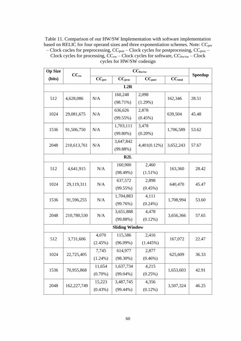
60
Table 11. Comparison of our HW/SW Implementation with software implementation
based on RELIC for four operand sizes and three exponentiation schemes. Note: CCpre
– Clock cucles for preprocessing, CCpost – Clock cycles for postprocessing, CCproc –
Clock cycles for processing, CCsw – Clock cycles for software, CChw/sw – Clock
cycles for HW/SW codesign
Op Size
(bits) CCsw
CChw/sw Speedup
CCpre CCproc CCpost CCtotal
L2R
512 4,628,086 N/A 160,248
(98.71%)
2,098
(1.29%) 162,346 28.51
1024 29,081,675 N/A 636,626
(99.55%)
2,878
(0.45%) 639,504 45.48
1536 91,506,750 N/A 1,703,111
(99.80%)
3,478
(0.20%) 1,706,589 53.62
2048 210,613,761 N/A 3,647,842
(99.88%) 4,401(0.12%) 3,652,243 57.67
R2L
512 4,641,915 N/A 160,900
(98.49%)
2,460
(1.51%) 163,360 28.42
1024 29,119,311 N/A 637,572
(99.55%)
2,898
(0.45%) 640,470 45.47
1536 91,596,255 N/A 1,704,883
(99.76%)
4,111
(0.24%) 1,708,994 53.60
2048 210,780,530 N/A 3,651,888
(99.88%)
4,478
(0.12%) 3,656,366 57.65
Sliding Window
512 3,731,606 4,070
(2.45%)
115,586
(96.09%)
2,416
(1.445%) 167,072 22.47
1024 22,725,405 7,745
(1.24%)
614,977
(98.30%)
2,877
(0.46%) 625,609 36.33
1536 70,955,868 11,654
(0.70%)
1,637,734
(99.04%)
4,215
(0.25%) 1,653,603 42.91
2048 162,227,749 15,223
(0.43%)
3,487,745
(99.44%)
4,356
(0.12%) 3,507,324 46.25
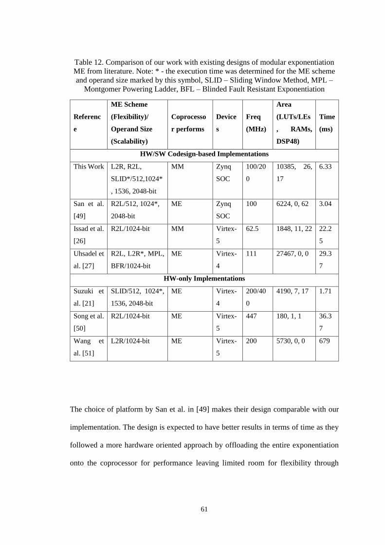
61
Table 12. Comparison of our work with existing designs of modular exponentiation
ME from literature. Note: * - the execution time was determined for the ME scheme
and operand size marked by this symbol, SLID – Sliding Window Method, MPL –
Montgomer Powering Ladder, BFL – Blinded Fault Resistant Exponentiation
Referenc
e
ME Scheme
(Flexibility)/
Operand Size
(Scalability)
Coprocesso
r performs
Device
s
Freq
(MHz)
Area
(LUTs/LEs
, RAMs,
DSP48)
Time
(ms)
HW/SW Codesign-based Implementations
This Work L2R, R2L,
SLID*/512,1024*
, 1536, 2048-bit
MM Zynq
SOC
100/20
0
10385, 26,
17
6.33
San et al.
[49]
R2L/512, 1024*,
2048-bit
ME Zynq
SOC
100 6224, 0, 62 3.04
Issad et al.
[26]
R2L/1024-bit MM Virtex-
5
62.5 1848, 11, 22 22.2
5
Uhsadel et
al. [27]
R2L, L2R*, MPL,
BFR/1024-bit
ME Virtex-
4
111 27467, 0, 0 29.3
7
HW-only Implementations
Suzuki et
al. [21]
SLID/512, 1024*,
1536, 2048-bit
ME Virtex-
4
200/40
0
4190, 7, 17 1.71
Song et al.
[50]
R2L/1024-bit ME Virtex-
5
447 180, 1, 1 36.3
7
Wang et
al. [51]
L2R/1024-bit ME Virtex-
5
200 5730, 0, 0 679
The choice of platform by San et al. in [49] makes their design comparable with our
implementation. The design is expected to have better results in terms of time as they
followed a more hardware oriented approach by offloading the entire exponentiation
onto the coprocessor for performance leaving limited room for flexibility through
62
software. We provide a more balanced partitioning scheme to exploit maximum benefit
from both hardware and software, still maintaining comparable performance.
In [26], a fixed 1024-bit RSA design is implemented with one exponentiation scheme,
i.e., R2L. They employ two multiplier units to optimize their design for R2L scheme.
This scheme cannot be easily generalized to show performance gain for other
exponentiation schemes. Also, their design is 3.5 times slower than our implementation.
In [27], results for HW/SW codesign-based implementation using 8051 microcontroller
are presented. Although they implement several exponentiation schemes, their design
is not scalable for any operand sizes other than 1024-bit. Our computation time is 4.6
times faster than their design based on L2R scheme.
We also provide HW only designs, implemented without the use of any embedded
processor. Their results do not offer a fair comparison as the designs are HW-only
implementations. In codesign-based approach, the designer should deal with additional
overheads related to communication interfaces. HW-only designs are more geared
towards optimizing for execution time and are less suited for applications that require
flexibility. The capability of controlling designs from software to can also help to
evaluate the best suited combination of parameters and schemes for an embedded
application with comparable performance. Implementing exponentiation algorithms
can also provide additional resistance against side-channel attacks.
63
4.6 Conclusion
We presented a novel HW/SW codesign approach to support algorithmic and
implementation level flexibility. The generic approach can be applied to other public-
key cryptosystems as well. In the current design, we achieved up to 57 times speedup
as compared to our software implementation with comparable performance in
hardware. The results show that balanced partitioning of a design between hardware
and software may seem challenging but it can support promising flexibility vs
performance tradeoff.
64
5 CUSTOM HARDWARE IMPLEMENTATION OF NTRUEncrypt
In this chapter, we present a high-speed hardware implementation of NTRUEncrypt
Short Vector Encryption Scheme (SVES), fully compliant with the IEEE 1363.1
Standard Specification for Public Key Cryptographic Techniques Based on Hard
Problems over Lattices. Our implementation supports two representative parameter
sets, ees1087ep1 and ees1499ep1, optimized for speed, which provide security levels
of 192 and 256 bits, respectively. Our implementation follows an earlier proposed Post-
Quantum Cryptography (PQC) Hardware Application Programming Interface (API).
As a first implementation following this API, it provides a reference that can be adopted
in any future implementations of post-quantum cryptosystems. We describe the detailed
flow and block diagrams as well as results in terms of latency (in clock cycles),
maximum clock frequency, and resource utilization. We also report the speedup of our
implementation in Xilinx Field Programmable Gate Arrays (FPGAs) as compared to a
software implementations of NTRUEncrypt SVES, with equivalent functionality,
running on the Cortex A9 ARM Core. Our results show a significant speed-up of
hardware vs. software, and very different percentage contributions of the execution
times for equivalent operations executed in these two different environments.
5.1 Preliminaries
We are not aware of any previous high-speed hardware implementation of the entire
NTRUEncrypt SVES scheme reported in the scientific literature or available
commercially. Our implementation is also unique in that it is the first implementation

65
of any PQC scheme following our newly proposed PQC Hardware API. As such, it
provides a valuable reference for any future implementers of PQC schemes, which is
very important in the context of the upcoming NIST standard candidate evaluation
process.
5.2 NTRUEncrypt SVES
The flow diagrams of the NTRUEncrypt SVES encryption and decryption operations
are shown in Figure 15. The notation used, and the names of basic operations, inputs,
outputs, and intermediate variables are explained in Table 13 and
Table 14.
8*l
B2T
octL p0
Mbin
db
b
8 8*p0Len
m
2N
2N
MGF2N
m
+2N
αN
2N
*
αN
r
αN
db
BPGM
m
24
OID
8*l
b hTrunc
pkLen
e
sData
αN
Mtrin
mask
Check 1
h
mod42N
+
m
R=r*hR4
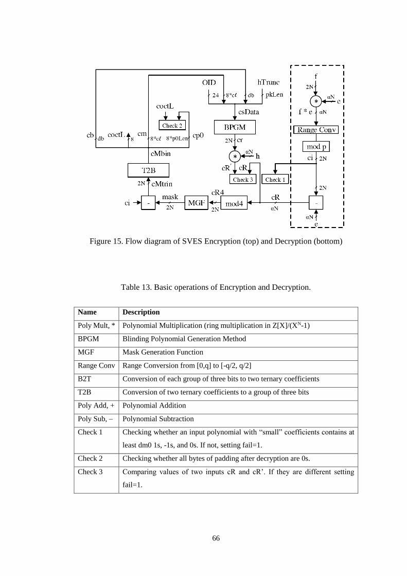
66
Figure 15. Flow diagram of SVES Encryption (top) and Decryption (bottom)
Table 13. Basic operations of Encryption and Decryption.
Name Description
Poly Mult, * Polynomial Multiplication (ring multiplication in Z[X]/(XN-1)
BPGM Blinding Polynomial Generation Method
MGF Mask Generation Function
Range Conv Range Conversion from [0,q] to [-q/2, q/2]
B2T Conversion of each group of three bits to two ternary coefficients
T2B Conversion of two ternary coefficients to a group of three bits
Poly Add, + Polynomial Addition
Poly Sub, – Polynomial Subtraction
Check 1 Checking whether an input polynomial with “small” coefficients contains at
least dm0 1s, -1s, and 0s. If not, setting fail=1.
Check 2 Checking whether all bytes of padding after decryption are 0s.
Check 3 Comparing values of two inputs cR and cR’. If they are different setting
fail=1.
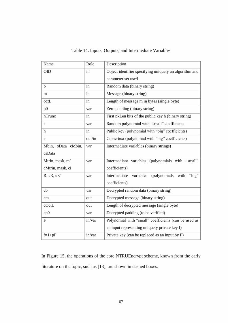
67
Table 14. Inputs, Outputs, and Intermediate Variables
Name Role Description
OID in Object identifier specifying uniquely an algorithm and
parameter set used
b in Random data (binary string)
m in Message (binary string)
octL in Length of message m in bytes (single byte)
p0 var Zero padding (binary string)
hTrunc in First pkLen bits of the public key h (binary string)
r var Random polynomial with “small” coefficients
h in Public key (polynomial with “big” coefficients)
e out/in Ciphertext (polynomial with “big” coefficients)
Mbin, sData cMbin,
csData
var Intermediate variables (binary strings)
Mtrin, mask, m’
cMtrin, mask, ci
var Intermediate variables (polynomials with “small”
coefficients)
R, cR, cR’ var Intermediate variables (polynomials with “big”
coefficients)
cb var Decrypted random data (binary string)
cm out Decrypted message (binary string)
cOctL out Length of decrypted message (single byte)
cp0 var Decrypted padding (to be verified)
F in/var Polynomial with “small” coefficients (can be used as
an input representing uniquely private key f)
f=1+pF in/var Private key (can be replaced as an input by F)
In Figure 15, the operations of the core NTRUEncrypt scheme, known from the early
literature on the topic, such as [13], are shown in dashed boxes.

68
In the SVES encryption scheme shown in Figure 15, m is replaced by m’, which is an
intermediate variable, dependent on the binary message m, length of m (denoted by
octL), random data b, public key h, and the Object identifier, OID, representing
uniquely a given encryption scheme and parameter set. Additionally, r is not selected
completely at random, but rather generated by a deterministic function, called the
Blinding Polynomial Generation Method (BPGM), based on a standardized hash
algorithm, with inputs in the form of OID, message m, random data b, and the first
pkLen bits of the public key h (hTrunc). B2T is a conversion of each group of three bits
to two ternary coefficients, using the look-up table defined in the IEEE standard.
In the SVES decryption scheme shown in Figure 15, the decrypted value is denoted by
ci, and must be still unmasked to recover the actual decrypted binary message cm. Three
checks are performed on the decryption side. If any of these checks fails, the result of
decryption is considered invalid. Check 1 is to verify whether ci, which should be
identical with m’ on the encryption site, has a sufficient number (at least dm0) of 1s, -
1s, and 0s (where dm0 is a part of a given parameter set, and is given in Table 3). Check
2 is to determine whether cMbin on the decryption side, which should be the same as
Mbin on encryption site, has a proper format, i.e., its padding bytes (the last
maxMsgLenBytes – cOctL bytes) are all equal to zeros. Finally, Check 3 is the most
comprehensive check, used to verify whether the value of cR’ is equal to cR, where cR’
is calculated using the same formulas as R during decryption, with the message m
replaced by decrypted message cm, and the random input b replaced by the decrypted
random data cb. The other parts of the input to BPGM, namely OID and hTrunc, remain
the same as during encryption. T2B is an inverse of the B2T conversion function.
69
5.3 Hardware Design
Assumptions
Our hardware implementation supports full Short Vector Encryption Scheme (SVES)
described in the IEEE P1361.1 standard [14]. It is also compliant with the recently
proposed PQC Hardware API [52]. Encryption and decryption share the same circuit.
Key generation is assumed to be performed externally, e.g., in software. This
assumption is consistent with the proposed PQC Hardware API [52], and is common
for many practical implementations of other public key cryptosystems. Public key and
private key are loaded in advance, before the first encryption/decryption. They are
stored internally and can be used for processing of multiple messages/ciphertexts.
The primary optimization target is the minimum latency (in absolute time units) for
encryption and decryption. However, in case any design choices can lead to the same
or only marginally greater latency, with the circuit area decreased substantially, these
design choices are pursued as well to keep the cost and energy consumption of the
circuit as low as possible.
The implementation supports two parameter sets, specified in [14], denoted as
ees1087ep1 and ees1499ep1, optimized for speed, with security levels of 192 and 256
bits, respectively. The swap between these two parameter sets can occur during runtime.
SHA-256 is used as a basis for the implementation of the Blinding Polynomial
Generation Method (BPGM) and the Mask Generation Function (MGF) of SVES. The
remaining major parameters of both sets are summarized in Table 15.
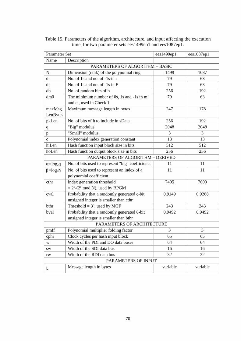
70
Table 15. Parameters of the algorithm, architecture, and input affecting the execution
time, for two parameter sets ees1499ep1 and ees1087ep1.
Parameter Set ees1499ep1 ees1087ep1
Name Description
PARAMETERS OF ALGORITHM – BASIC
N Dimension (rank) of the polynomial ring 1499 1087
dr No. of 1s and no. of -1s in r 79 63
df No. of 1s and no. of -1s in F 79 63
db No. of random bits of b 256 192
dm0 The minimum number of 0s, 1s and -1s in m’
and ci, used in Check 1
79 63
maxMsg
LenBytes
Maximum message length in bytes 247 178
pkLen No. of bits of h to include in sData 256 192
q "Big" modulus 2048 2048
p "Small" modulus 3 3
c Polynomial index generation constant 13 13
hiLen Hash function input block size in bits 512 512
hoLen Hash function output block size in bits 256 256
PARAMETERS OF ALGORITHM – DERIVED
=log2q No. of bits used to represent "big" coefficients 11 11
=log2N No. of bits used to represent an index of a
polynomial coefficient
11 11
cthr Index generation threshold
= 2c-(2c mod N), used by BPGM
7495 7609
cval Probability that a randomly generated c-bit
unsigned integer is smaller than cthr
0.9149 0.9288
bthr Threshold = 35, used by MGF 243 243
bval Probability that a randomly generated 8-bit
unsigned integer is smaller than bthr
0.9492 0.9492
PARAMETERS OF ARCHITECTURE
pmff Polynomial multiplier folding factor 3 3
cphi Clock cycles per hash input block 65 65
w Width of the PDI and DO data buses 64 64
sw Width of the SDI data bus 16 16
rw Width of the RDI data bus 32 32
PARAMETERS OF INPUT
L Message length in bytes variable variable

71
Both polynomial r (for encryption) and polynomial F (for decryption) are
represented using indices of all their coefficients equal to 1 and -1. Our implementation
does not support the so-called product form of polynomials r and F, described in [16],
as this form is not supported by P1363.1 [14].
5.3.1 Hardware API & Interface of NTRU core
To ensure compatibility among implementations of the same algorithm by different
designers, our NTRU implementation is designed based on the hardware API proposed
in [52]. A general idea of the NTRU core interface is shown in Figure 16.
NTRU
do_data do_dataw
pdipdiw
pdi_validpdi_valid
pdi_readypdi_ready
sdisdisw
sdi_validsdi_valid
sdi_readysdi_ready
rdirdirw
rdi_validrdi_valid
rdi_readyrdi_ready
do_valid do_valid
do_ready do_ready
mem_addr
mem_do
mem_di
mem_wr
status_ready
clk rst
clk rst
amw
mw
mw
wmw
Figure 16. NTRU Interface compatible with the PQC Hardware API interface [8].
The interface has five major data buses: 1) Public Data Inputs (PDI), 2) Secret Data
Inputs (SDI), 3) Random Data Inputs (RDI), 4) Data Outputs (DO), and 5) External
memory Inputs/Outputs (MEM), respectively. The external memory ports are optional,
and are not used by our core. Selected widths of the interface data buses, w, sw, and rw
are summarized in Table 3. These widths were selected in such a way to minimize the
time required to load inputs and unload results, but at the same time, keep the pin
requirements of the circuit at the level easily supported by modern FPGAs. Private key
72
is assumed to be loaded through SDI in the form of –bit indices of the non-zero
coefficients of F, one coefficient at a time. Public key is loaded through PDI.
5.3.2 Top-Level Block Diagram
The top-level hardware block diagram is shown in Figure 17. The function of the
majority of operational units corresponds to the basic operations of encryption and
decryption, specified in Table 13. The functionality of additional auxiliary components
is summarized in Table 16.
The two major functional units, which determine the speed and area of the circuit are
PolyMult and BPGM/MGF. The latter of these units is used to implement both BPGM
and MGF, because of the similarity between both operations, their sequential non-
overlapping functionality, and because of the reliance on a single hash function core,
implementing SHA-256.
Public key h is stored inside of Poly Mult (for both encryption and decryption). Indices
of non-zero coefficients of F, uniquely determining the private key f, are stored in RAM
at the top level (located in the diagram in Figure 17 just above the Poly Mult unit).
Range Conversion and modulo p reduction are naturally combined together. The mod
p (mod 3) operation is optimized in such a way to use just 10 LUTs per 11-bit
coefficient.
Poly Add (+), Poly Sub (-), Range Conv & mod p, T2B, Check 1 and Check 3 are all
performed on only 2w (rather than N) coefficients at a time. Since these operations do
not limit the latency of either Encryption or Decryption (as long as performed at least
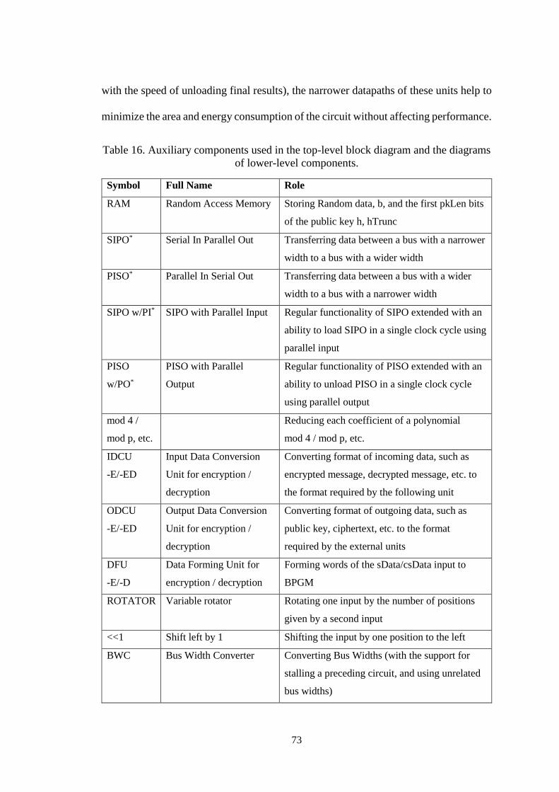
73
with the speed of unloading final results), the narrower datapaths of these units help to
minimize the area and energy consumption of the circuit without affecting performance.
Table 16. Auxiliary components used in the top-level block diagram and the diagrams
of lower-level components.
Symbol Full Name Role
RAM Random Access Memory Storing Random data, b, and the first pkLen bits
of the public key h, hTrunc
SIPO* Serial In Parallel Out Transferring data between a bus with a narrower
width to a bus with a wider width
PISO* Parallel In Serial Out Transferring data between a bus with a wider
width to a bus with a narrower width
SIPO w/PI* SIPO with Parallel Input Regular functionality of SIPO extended with an
ability to load SIPO in a single clock cycle using
parallel input
PISO
w/PO*
PISO with Parallel
Output
Regular functionality of PISO extended with an
ability to unload PISO in a single clock cycle
using parallel output
mod 4 /
mod p, etc.
Reducing each coefficient of a polynomial
mod 4 / mod p, etc.
IDCU
-E/-ED
Input Data Conversion
Unit for encryption /
decryption
Converting format of incoming data, such as
encrypted message, decrypted message, etc. to
the format required by the following unit
ODCU
-E/-ED
Output Data Conversion
Unit for encryption /
decryption
Converting format of outgoing data, such as
public key, ciphertext, etc. to the format
required by the external units
DFU
-E/-D
Data Forming Unit for
encryption / decryption
Forming words of the sData/csData input to
BPGM
ROTATOR Variable rotator Rotating one input by the number of positions
given by a second input
<<1 Shift left by 1 Shifting the input by one position to the left
BWC Bus Width Converter Converting Bus Widths (with the support for
stalling a preceding circuit, and using unrelated
bus widths)

74
*Nsel control input is optionally used if either input or output bus width depends on N. This input modifies the
operation of the circuit depending on the currently used value of N, corresponding to one of the two supported
parameter sets.
Figure 17. Top-level block diagram of the developed hardware architecture of SVES.
N represents max(1499, 1087)=1499.
Before the first exchange of data with a given user, this user’s public key must be loaded
to the PolyMult unit, using the pdi_data bus, and the Input Data Conversion Unit
(IDCU-ED). This unit is required to handle the control signals of the PDI bus and to
perform the bus width conversion (from w to w/ bits). Similarly, before
decrypting first data from a given user, this user’s private key value, F, must be loaded
to the circuit using the sdi_data bus, and stored in the internal RAM. Since F is a
polynomial with small coefficients 1, -1, and 0, only the locations of 1s and -1s must
75
be loaded. Each of these locations is a number in the range, 0..N-1, and thus is
represented using =ceil(log2N) bits. Each location is loaded in a separate clock cycle.
During encryption, the db bits of random data b are first loaded to the RAM with the
input rdi_data. The sData input to BPGM is formed next, as the concatenation of OID
(Object identifier), b, m (message), and hTrunc (the first pkLen bits of the public key
h), using the Data Formation Unit, DFU-E. After being fed with sData as a seed, BPGM
works as a pseudorandom number generator, producing a new location i of a non-zero
small coefficient of the random polynomial r in each new iteration of BPGM. Each of
these locations is consumed by PolyMult in 3 clock cycles, corresponding to the
Polynomial multiplier folding factor, pmff. Only after PolyMult processes all elements
of r, the output R=r*h becomes available. This output is then reduced mod 4, and the
obtained values provided to the input of MGF. The MGF unit produces the mask, in the
form of a polynomial with small random coefficients. This polynomial is then added to
the polynomial mTrin obtained by converting the extended message input Mbin=b,
octL, m, p0, using the binary to ternary conversion unit, B2T. Finally, the obtained new
message representation, m’, is added to the previously generated output from PolyMul,
R, producing the ciphertext e. The ciphertext is than released to the output do_data,
after conversion to words of the width w, using PISO and the Output Data Conversion
Unit (ODCU-E).
The decryption, starts from the polynomial multiplication of the private key f=1+pF by
the ciphertext e. The obtained value fe then undergoes range conversion and reduction
mod p. The obtained value ci should be the same as the message representation during
encryption m’. ci undergoes Check 1 for the minimum number of 1s, -1s, and 0s.

76
Additionally, ci is used in the calculation of cR=e-ci, which should be identical to R,
calculated on the encryption side. cR is then reduced mod 4 and used as an input to
MGF to produce mask. Mask is subtracted from ci to generate cMtrin. After converting
cMtrin to cMbin using the ternary to binary conversion T2B and a PISO. The Output
Data Conversion Unit (ODCU-D & Check 2) checks whether the decrypted data has a
correct format, including p0Len= maxMsgLenBytes – cOctL bytes of zero padding. If
Check 2 passes, the extended decrypted data is decoded to identify values of cb and cm,
which should be the same as b and m during encryption. These values are then used as
inputs to the Data Formation Unit for Decryption (DFU_D), used to generate csData =
OID, cm, cb, hTrunc. csData is then passed to BPGM as a seed value. The BPGM unit
then produces the locations i of all non-zero coefficients of the random polynomial cr=r,
which should be the same as those on the encryption site. These values are then used,
together with the public key h, stored inside of Poly Mult, to calculate cR’=cr*h. Since
for the correctly decrypted message, cr=r, then cR’ should be equal to cR obtained
earlier during the decryption process. Comparing these two values constitutes the final
check (Check 3) for the correctness of decryption. Only after this test passes, the
decrypted message cm is released through the output do_data, followed by the status
block with the Status field equal to Success. If any of the three decryption checks fails,
all remaining calculations are preempted and only the status block with the Status field
equal to Failure is released to the output do_data.
5.3.3 Diagrams of Selected Lower-Level Components
Internal block diagrams of two major components: the polynomial multiplier, Poly
Mult, and the BPGM/MGF units are shown in Figure 18 and Figure 19, respectively.
77
The polynomial multiplier is based on a variable rotator, and a series of adders capable
of adding a corresponding coefficient of one of the operands to a temporary sum. A full
width version of this multiplier can be folded by an arbitrary factor. A folding factor
equal to 3, which was selected based on the careful timing analysis, is shown in Figure
18.
During encryption, only one polynomial multiplication R=r*h is performed, and thus,
the public key h can be stored directly in the top SIPO w/PI (the Serial Input Parallel
Output unit with Parallel Input). During decryption, two multiplications are performed,
f*e and cR’=cr*h. As a result during the first multiplication, h is pushed to the
neighboring PISO w/PO (the Parallel Input Serial Output unit with Parallel Output),
and then brought back to SIPO w/PI for the second polynomial multiplication. In the
period between the two multiplications, PISO w/PO (holding the ciphertext e), feeding
the serial output ce, is used for the calculation of cR (2w -bit coefficients at a time).
The BPGM/MGF unit is shown in Figure 19. It is based on the slightly modified
implementation of SHA-256 [53], extended with the capability to store and retrieve the
chaining value, which substantially speeds up the repeated computations of
hash(Z||Counter) for multiple values of the Counter and Z composed of multiple input
blocks of SHA-256.
Our implementation of SHA-256 is a basic iterative architecture with 65 clock cycles
per block. During the BPGM calculations Data input is used. During the MGF
calculations, the inputs R4 and cR4 are used, for encryption and decryption,
respectively. For the BPGM calculations, the output of a hash function is divided into
c-bit blocks (with c=13 for both implemented parameter sets). Each block is treated as

78
an unsigned integer. If the value of this integer is greater than the index generation
threshold cthr = 2c-(2c mod N), then the block is discarded. Otherwise, the
corresponding output i is calculated by taking the unsigned integer value of the block
mod N. Since N is different for each parameter set (1499 and 1087, respectively), two
2c x look-up tables are required to perform the respective mod operations.
Figure 18. Architecture of the polynomial multiplier, folded by a factor of 3

79
Figure 19. Hardware architecture of the combined unit, BPGM/MGF, implementing
the Blinding Polynomial Generation Method and Mask Generation Function
5.4 Results
Our design has been described in VHDL at the Register Transfer Level (RTL). The
target device has been selected as Xilinx Virtex-7 XC7VX485T-3FFG1761. The results
have been generated using Xilinx ISE v14.7. All presented results are after placing and
routing.
In Table 17, we summarize the resource utilization (in LUTs and Slices), maximum
clock frequency, and latencies of several major building blocks. Poly Mult is shown to
be most restrictive in terms of clock frequency (89.51 MHz) and taking a vast majority

80
of the circuit resources (138,475 LUTs). It should be stressed that for operations such
as Poly Add and Poly Sub, latency represents the number of clock cycles necessary to
obtain an output coefficient corresponding to the input coefficients with the same index,
and not the time necessary to process all coefficients of the polynomial.
Table 17. Resource utilization and performance metrics of major component units.
Latencies correspond to the ees1499ep1 parameter set.
Operation LUTs: Slices Clk Freq
[MHz]
Latency
[cycles]
Latency·LUTs
Poly Mult 140,512: 25,099
74.44 474 66,602,688
BPGM 1971: 421 171.05 845 1,665,495
MGF 1004 1,978,884
B2T 64: 34 904.00 1 64
T2B 64: 35 984.25 1 64
Poly Adds
e=(Mtrin+mask) +R_fe
1338: 272
316.25 1 1338
Poly Sub
cMtrin=ci-mask
74 : 64 540.24 1 74
Poly Sub
cR=ce-ci
1221 : 258 331.23 1 1221
Timing analysis of our hardware implementation is shown in Table 18. Latencies in
clock cycles correspond to the maximum sizes of messages allowed by a given
parameter set. For comparison, in Table 19, we present the results of profiling of the
software implementation of NTRUEncrypt SVES from [54], using the Cortex A9
ARM Core, with clock cycles measured using a 100 MHz, AXI Timer.
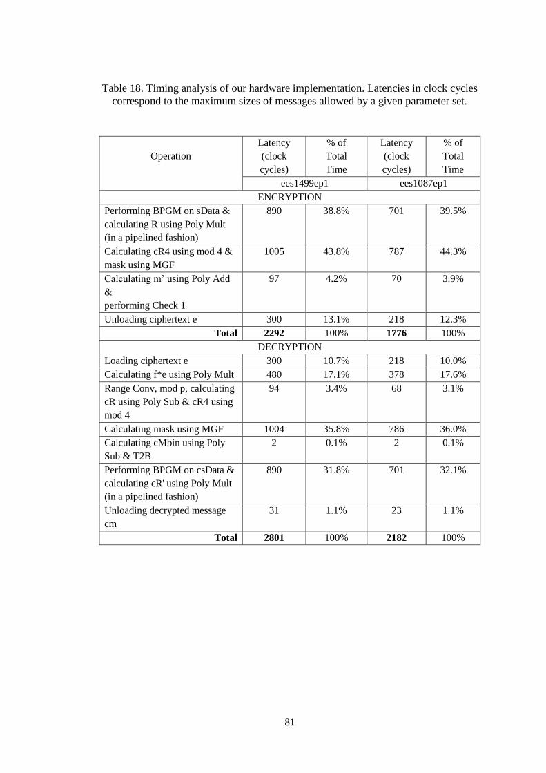
81
Table 18. Timing analysis of our hardware implementation. Latencies in clock cycles
correspond to the maximum sizes of messages allowed by a given parameter set.
Operation
Latency
(clock
cycles)
% of
Total
Time
Latency
(clock
cycles)
% of
Total
Time
ees1499ep1 ees1087ep1
ENCRYPTION
Performing BPGM on sData &
calculating R using Poly Mult
(in a pipelined fashion)
890 38.8% 701 39.5%
Calculating cR4 using mod 4 &
mask using MGF
1005 43.8% 787 44.3%
Calculating m’ using Poly Add
&
performing Check 1
97 4.2% 70 3.9%
Unloading ciphertext e 300 13.1% 218 12.3%
Total 2292 100% 1776 100%
DECRYPTION
Loading ciphertext e 300 10.7% 218 10.0%
Calculating f*e using Poly Mult 480 17.1% 378 17.6%
Range Conv, mod p, calculating
cR using Poly Sub & cR4 using
mod 4
94 3.4% 68 3.1%
Calculating mask using MGF 1004 35.8% 786 36.0%
Calculating cMbin using Poly
Sub & T2B
2 0.1% 2 0.1%
Performing BPGM on csData &
calculating cR' using Poly Mult
(in a pipelined fashion)
890 31.8% 701 32.1%
Unloading decrypted message
cm
31 1.1% 23 1.1%
Total 2801 100% 2182 100%

82
Table 19. Results of profiling of the software implementation of NTRUEncrypt SVES
from [9], using the Cortex A9 ARM Core of Zynq 7020, for the ees1499ep1parameter
set
Software Function Hardware Equivalent Clock
cycles
% of
Total
Time
ntru_gen_poly Performing BPGM on sData &
calculating R using Poly Mult
(in a pipelined fashion)
24,779 2.3%
ntru_octets_2_elements 12,728 1.2%
ntru_ring_mult_product_in
dices
950,892 89.4%
ntru_coeffs_mod4_2_octet
s
Calculating cR4 using mod 4 &
mask using MGF
9,427 0.9%
ntru_mgftp1 30,703 2.9%
ntru_bits_2_trits 3,020 0.3%
adding Mtrin to mask Calculating m’ using Poly Add &
performing Check 1
8,108 0.8%
ntru_poly_check_min_wei
ght
6,910 0.6%
add_m' 8,672 0.8%
elements_2_octets Unloading ciphertext e 13,549 1.3%
Total 1,068,788 100.0%
The percentage contribution of various operations is substantially different for
hardware and software implementation. Hardware implementation is seriously limited
by the sequential nature of the SHA-256 calculations. As a result, the operation of Poly
Mult can be almost completely overlapped with the computations of BPGM through
the use of pipelining. On the other hand, in the software implementation, Poly Mult
amounts to about 90% of the total execution time. The operations that are most critical
in hardware are hash based operations of BPGM and MGF, amounting to about 83% of
the execution time for both supported parameter sets.

83
Table 20. Speed up of Hardware (This Work) vs. Software (source code [54])
Software Hardware Speed-up
Poly Mult [s] 9,508.9 5.3 x1794.1
No. of Poly Mults per second 105.2 188,679.2
Encryption Time [s] 10,687.9 25.6 x417.5
No. of Encryptions per second 93.6 39,062.5
The speed up of our hardware implementation vs. software implementation from [54],
running on the Cortex A9 ARM Core of Zynq 7020, with the clock frequency of
666.7 MHz, is summarized in Table 20. For Poly Mult, this speed-up reaches almost
1800. For the entire encryption operation it is equal to 417.5.
The implementation results for NTRUEncrypt reported earlier in the literature are
summarized in Table 21. These results cannot be compared fairly with our results for
multiple reasons, such as: a) different security level (57 & 80 bits vs. 192 & 256 bits),
b) very different values of primary parameters (N=167 & 251 vs. N= 1499 & 1087,
q=128 vs. q=2048), c) implementation of a pure NTRUEncrypt vs. implementation of
NTRUEncrypt SVES), d) support for encryption only vs. support for encryption and
decryption, e) support for a single parameter set vs. support for two parameter sets
(swappable during run-time), f) results for old generation FPGA families (Virtex-E)
and ASIC libraries (0.13m) vs. results for the state-of-the-art FPGA family (Virtex-7,
28nm).
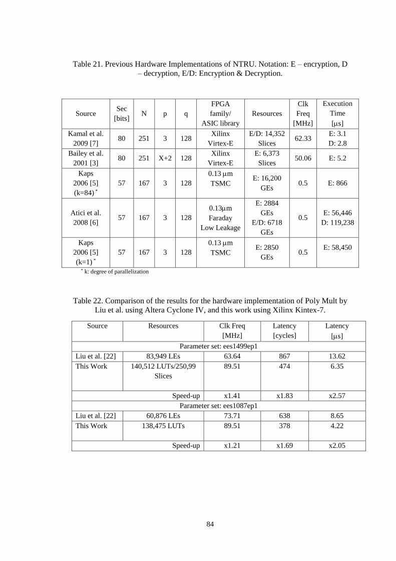
84
Table 21. Previous Hardware Implementations of NTRU. Notation: E – encryption, D
– decryption, E/D: Encryption & Decryption.
Source Sec
[bits] N p q
FPGA
family/
ASIC library
Resources
Clk
Freq
[MHz]
Execution
Time
[s]
Kamal et al.
2009 [7] 80 251 3 128
Xilinx
Virtex-E
E/D: 14,352
Slices 62.33
E: 3.1
D: 2.8
Bailey et al.
2001 [3] 80 251 X+2 128
Xilinx
Virtex-E
E: 6,373
Slices 50.06 E: 5.2
Kaps
2006 [5]
(k=84) *
57 167 3 128
0.13 m
TSMC
E: 16,200
GEs 0.5 E: 866
Atici et al.
2008 [6] 57 167 3 128
0.13m
Faraday
Low Leakage
E: 2884
GEs
E/D: 6718
GEs
0.5 E: 56,446
D: 119,238
Kaps
2006 [5]
(k=1) *
57 167 3 128
0.13 m
TSMC
E: 2850
GEs 0.5
E: 58,450
* k: degree of parallelization
Table 22. Comparison of the results for the hardware implementation of Poly Mult by
Liu et al. using Altera Cyclone IV, and this work using Xilinx Kintex-7.
Source Resources Clk Freq
[MHz]
Latency
[cycles]
Latency
[s]
Parameter set: ees1499ep1
Liu et al. [22] 83,949 LEs 63.64 867 13.62
This Work 140,512 LUTs/250,99
Slices
89.51 474 6.35
Speed-up x1.41 x1.83 x2.57
Parameter set: ees1087ep1
Liu et al. [22] 60,876 LEs 73.71 638 8.65
This Work 138,475 LUTs
89.51 378 4.22
Speed-up x1.21 x1.69 x2.05
85
The comparison of this work with the results reported in [55] for Poly Mult itself,
summarized in Table 22, demonstrates the speed-up by a factor of 2.57 for the
ees1499ep1 parameter set, and 2.05 for the ees1499ep1 parameter set. However, a
portion of this speed up has to be attributed to a different FPGA family: Xilinx Virtex-
7 in this work and Altera Cyclone IV in [55].
Since our implementation is intended primarily for high-end servers supporting a very
large number of TLS, IPSec, and other secure protocol transactions per second, no
attempt was made to introduce any countermeasures against side channel attacks. Still
making the implementation constant-time might be desirable [56].
The current implementation has a natural dependence of the execution time on the
length of the message, affecting the size of sData and csData inputs to BPGM. For
example, for the ees1499ep1 parameter set, the latency of encryption varies between
2097 clock cycles for an empty message, and 2292 clock cycles for the maximum
allowed size of the message (247 bytes). Eliminating this dependence will be a part of
our future work.
5.5 Conclusions
We report the first high-speed hardware implementation of the full encryption scheme
of the IEEE P1363.1 standard (NTRUEncrypt SVES).
Our results demonstrate the need to revisit the algorithmic construction of the
NTRUEncrypt SVES in order to make this algorithm more parallelizable and more
suitable for high-speed hardware implementations in the post-quantum era.
86
It should be noticed that the similar problem has been earlier reported by Gueron et al.
[57], for software implementations taking advantage of the AVX2 and AVX512 Single
Instruction Multiple Data (SIMD) instructions of modern Intel processsors. The
proposed solution was to replace the SHA-1/SHA-256 hash functions with the
pseudorandom function based on the pipelined AES New Instructions (AES-NI).
Although this solution may be also applicable to hardware implementations, other
alternatives, preserving the desired security features, but offering a greater potential for
parallelization of the BPGM and MGF functions should be considered as well. For
example, the use of the hardware friendly SHA-3 functions may be considered.
Natural resistance to timing attacks could be added as well through algorithmic changes
in the NTRUEncrypt SVES scheme by eliminating the dependence of the size of inputs
sData and csData to BPGM on the length of the message.
Additionally, the elimination of the use of SHA-1 in the P1363.1 parameter sets with the
security levels of 112 and 128 bits should be taken into account, both for security reasons
[58], as well as in order to avoid any undesired hardware overhead associated with
implementing multiple hash algorithms within one generic hardware module supporting
multiple parameter sets.
Our future work will involve taking advantage of any additional optimizations at the
algorithmic and hardware architecture levels (including the possible use of unrolled
implementations of SHA-2, with two or more rounds per clock cycle [59]), adding
countermeasures against timing attack [56], as well as targeting minimum energy use.

87
6 Hardware/ Software Codesign of NTRUEncrypt
This chapter focusses on the Hardware/Software codesign of NTRU cryptosystem. We
demonstrate our design methodology, focusing on finding an optimal partitioning
scheme to offload the computationally intensive operations to the programmable logic.
We discussed the input and output interface we adopted for our codesign
implementation. The critical path analysis of our design was conducted and based on
that, we explain our efforts to optimally pipeline our design to achieve maximum
frequency. Eventually, we attempted different techniques to reduce the area utilization
of our polynomial multiplier We conclude the discussion by providing results for our
codesign implementation.
6.1 Methodology
To fit the design on our Zedboard platform (Zynq-7000) that has an Artix-7 FPGA, we
conduct this research on NTRU codesign by adopting a smaller parameter set
EES401EP1. Using larger parameter sets that take resources more than available in the
programmable logic of our current platform, limits our capability to fit the design inside
the FPGA during the implementation phase. To avoid this constraint and allow
successful implementation and routing of the design, the HW/SW codesign results are
taken using a smaller parameter set in which the resources take close to 60% of the total
chip reconfigurable resources.
Once different optimization techniques are perfected, we intend to apply them to
designs with bigger parameter sets, EES1499EP1 and EES1499EP1.

88
6.2 Software Profiling
The results collected through software profiling show that polynomial multiplier takes
90 % of the total computation time. Based on this fact, it becomes a suitable operation
to be implemented in reconfigurable logic resources of FPGA.
6.3 Proposed Partitioning Schemes:
We proposed four schemes to partition NTRU.

89
Figure 20. Partitioning Schemes for HW/ SW Codesign of NTRU

90
6.4 Four popssible partitioning schemes NTRUEncrypt bewteen software
and hardware
The figure above shows the possible partitioning schemes for out NTRUEncrypt
implementation.
• Scheme 1: Offers full flexibility, but low performance
• Scheme 2: Only polynomial multiplication is offloaded to the coprocessor for
improved performance
• Scheme 3: Polynomial multiplication and combined BPGM/ MGF modules
are offloaded to the coprocessor for improved performance
• Scheme 4: Maximum performance gain possible with very limited flexibility
We implement partitioning scheme 2 as it leaves more room to achieve the balance
between flexibility through software and performance from the coprocessor.
POLY
MULT
do_data do_dataw
di_dataw
di_valid
di_ready
do_valid do_valid
do_ready do_ready
clk rst
clk rst
di_last
di_data
di_valid
di_ready
di_last do_last do_last
Figure 21. Interface for Polynomial Multiplier
91
For the HW/ SW codesign implementation of NTRU, we used AXI Stream interface to
to connect to input and output signals of the polynomial multiplier. In case of
encryption, we transmit the input data i.e public key “h” and indices of non-zero
coefficients of blinding polynomial “r” from PS to PL using the following function calls
1. load_h_e()
2. load_r_f()
Loading public key is not a part of encryption. It happens as a part of a separate function
call, load_h_e (), before any message is encrypted. With a FIFO at the input pdi_data,
we overlap the multiplication and the transmission of the indices of non-zero
coefficients of r.
6.5 Optimizing the Polynomial Multiplier
Different optimization techniques are employed to improve the performance and reduce
the area utilization of the design. These techniques are also application to hardware only
implementation of our design. We reduce the critical path of the hardware coprocessor
resulting in eventual speedup. The figure below shows the block diagram of the full
version of polynomial multiplier with maximum area utilization.
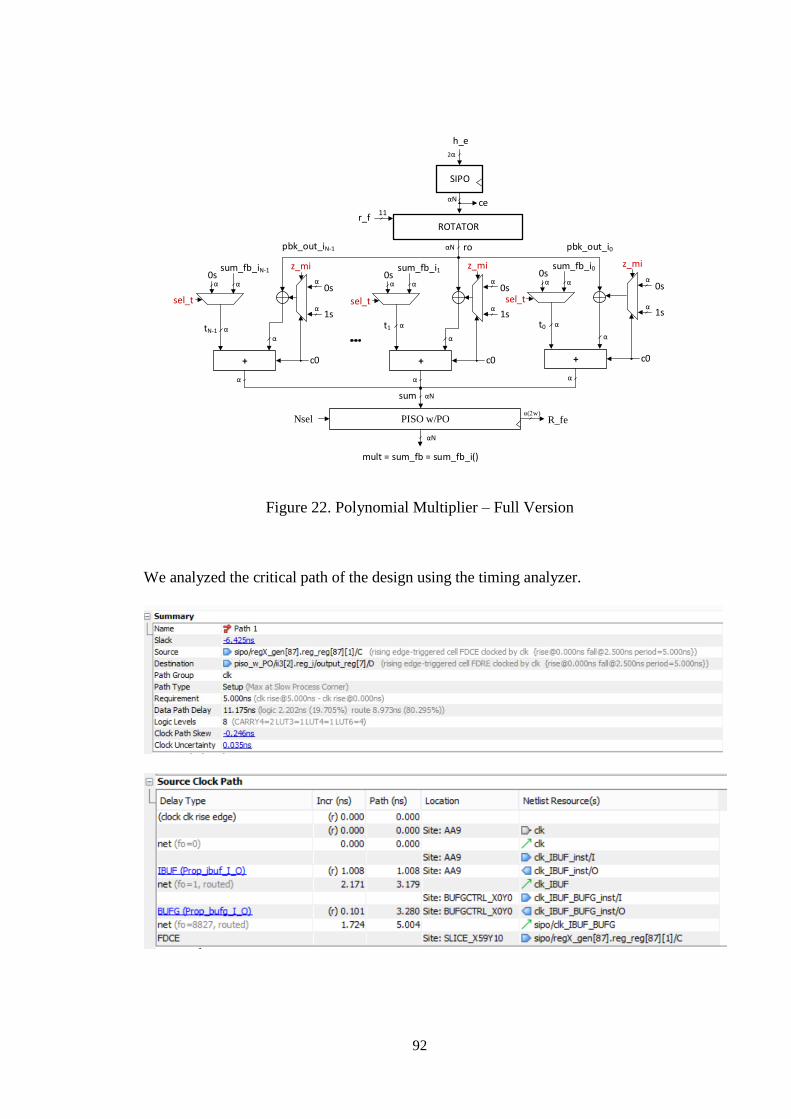
92
αN
+
ROTATOR
11
α
αN
mult = sum_fb = sum_fb_i()
0s
sum
α
ro
r_f
c0
0s
1s
α
α
h_e2α
SIPO
αN
α
α
sum_fb_i0
+
α
α
0sα
c0
0s
1s
α
α
α
α
sum_fb_i1
+
α
α
0sα
c0
0s
1s
α
α
α
α
sum_fb_iN-1
ce
sel_t sel_t sel_t
z_mi z_mi z_mi
tN-1t1 αt0
pbk_out_i0pbk_out_iN-1
PISO w/PO
αN
R_feα(2w)
Nsel
Figure 22. Polynomial Multiplier – Full Version
We analyzed the critical path of the design using the timing analyzer.
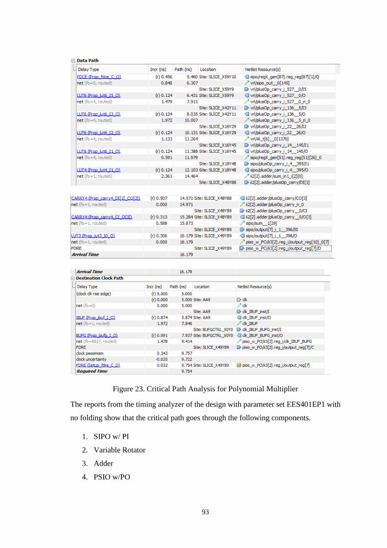
93
Figure 23. Critical Path Analysis for Polynomial Multiplier
The reports from the timing analyzer of the design with parameter set EES401EP1 with
no folding show that the critical path goes through the following components.
1. SIPO w/ PI
2. Variable Rotator
3. Adder
4. PSIO w/PO

94
αN
+
ROTATOR
11
α
αN
mult = sum_fb = sum_fb_i()
0s
sum
α
ro
r_f
c0
0s
1s
α
α
h_e2α
SIPO
αN
POLYNOMIAL MULTIPLIER – FULL WIDTH
α
α
sum_fb_i0
+
α
α
0sα
c0
0s
1s
α
α
α
α
sum_fb_i1
+
α
α
0sα
c0
0s
1s
α
α
α
α
sum_fb_iN-1
ce
sel_t sel_t sel_t
z_mi z_mi z_mi
tN-1t1 αt0
pbk_out_i0pbk_out_iN-1
PISO w/PO
αN
R_feα(2w)
Nsel
Figure 24. Full version of the multiplier (Critical Path shown in Red).
Out of these components, variable rotator introduced 46.2 % of the total delay. We tried
pipelining our variable rotator at various pipeline levels and analyzed the critical path.
Figure 25. Diagram for Pipelining at different Pipeline Levels
>> α*(2^0)
αN
>> α*(2^1)
αN
>> α*(2^5)
αN
>> α*(2^6)
αN
>> α*(2^7)
αN
>> α*(2^8)
αN
αN
A
C
>> α*(2^0)
αN
>> α*(2^1)
αN
>> α*(2^5)
αN
>> α*(2^6)
αN
>> α*(2^7)
αN
>> α*(2^8)
αN
αN
A
C
>> α*(2^0)
αN
>> α*(2^1)
αN
>> α*(2^5)
αN
>> α*(2^6)
αN
>> α*(2^7)
αN
>> α*(2^8)
αN
αN
A
C
>> α*(2^0)
αN
>> α*(2^1)
αN
>> α*(2^5)
αN
>> α*(2^6)
αN
>> α*(2^7)
αN
>> α*(2^8)
αN
αN
A
C
Variable Rotator – PL8Non-Pipelined – Variable Rotator Variable Rotator – PL7 Variable Rotator – PL6
Pipeline Level 8
Pipeline Level 7
Pipeline Level 6

95
It was evident that the pipelining the variable rotator at the pipeline level gave us the
best results and the critical path was balanced. This way, we could double the operating
frequency of the polynomial multiplier with a minimal penalty in terms of hardware
resource.
Secondly, we attempt to reduce area utilization of polynomial multiplier reduce the area
utilization in terms of number of CLB slices and LUTs. This is because it takes the
largest amount of area resources.
αN/3
PISO w/PO
α
+
ROTATOR
α
αN/3
p1
α
0s p20αα
c0
0s
1s
α
α
POLYNOMIAL MULTIPLIER – FOLDED BY 3
αN/3 αN/3αN/3
α
αN/3 αN/3 p0p2
p10α
p00α
α
+
α
α
0s p2N/3-1αα
c0
0s
1s
α
α
αp1N/3-1
α
p0N/3-1α
pj0pjN/3-1
<< 1
α
+
α
α
0s p21αα
c0
0s
1s
α
α
αp11
α
p01α
pj1
<< 1<< 1
αN
β
r_f
h_eSIPO w/PIαN
Nsel
PISO w/PO
αN/3
αN/3αN/3
R_feα(2w)
αN
ceα(2w)
Nsel
α* w/α
Figure 26. Polynomial Multiplier – Folded Architecture
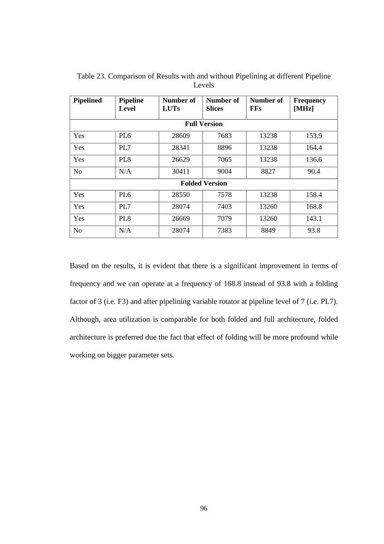
96
Table 23. Comparison of Results with and without Pipelining at different Pipeline
Levels
Pipelined Pipeline
Level
Number of
LUTs
Number of
Slices
Number of
FFs
Frequency
[MHz]
Full Version
Yes PL6 28609 7683 13238 153.9
Yes PL7 28341 8896 13238 164.4
Yes PL8 26629 7065 13238 136.6
No N/A 30411 9004 8827 90.4
Folded Version
Yes PL6 28550 7578 13238 158.4
Yes PL7 28074 7403 13260 168.8
Yes PL8 26669 7079 13260 143.1
No N/A 28074 7383 8849 93.8
Based on the results, it is evident that there is a significant improvement in terms of
frequency and we can operate at a frequency of 168.8 instead of 93.8 with a folding
factor of 3 (i.e. F3) and after pipelining variable rotator at pipeline level of 7 (i.e. PL7).
Although, area utilization is comparable for both folded and full architecture, folded
architecture is preferred due the fact that effect of folding will be more profound while
working on bigger parameter sets.

97
Figure 27. Reconfigurable Resource Utilization of Zynq SoC for HW/ SW Codesign
Implementation
Table 24. Results of profiling of the software implementation of NTRUEncrypt
SVES, using the Cortex A9 ARM Core of Zynq 7020, for the ees401ep1 parameter
set
Software Function Hardware Equivalent Clock
cycles
% of
Total
Time
ntru_gen_poly Performing BPGM on sData &
calculating R using Poly Mult
(in a pipelined fashion)
18081 3.9%
ntru_octets_2_elements 5558 1.2%
ntru_ring_mult_product_indices 407,988 88.0%
ntru_coeffs_mod4_2_octets Calculating cR4 using mod 4 & mask
using MGF 4636 1.0%
ntru_mgftp1 6027 1.3%
ntru_bits_2_trits 1391 0.3%
adding Mtrin to mask Calculating m’ using Poly Add &
performing Check 1 4173 0.9%
ntru_poly_check_min_weight 2318 0.5%
add_m' 3014 0.6%
elements_2_octets Unloading ciphertext e 5569 1.2%
Total 458,754 100.0%

98
Table 25. Results of profiling of the HW/ SW codesign implementation of
NTRUEncrypt SVES, using the Cortex A9 ARM Core of Zynq 7020, for the
ees401ep1 parameter set
Software Function Hardware Equivalent Clock
cycles
% of
Total
Time
ntru_gen_poly Performing BPGM on sData &
calculating R using Poly Mult
(in a pipelined fashion)
18081 35.0%
ntru_octets_2_elements 5558 10.8%
ntru_ring_mult_product_indices 857 1.7%
ntru_coeffs_mod4_2_octets Calculating cR4 using mod 4 & mask
using MGF 4636 9.0%
ntru_mgftp1 6027 11.7%
ntru_bits_2_trits 1391 2.7%
adding Mtrin to mask Calculating m’ using Poly Add &
performing Check 1 4173 8.1%
ntru_poly_check_min_weight 2318 4.5%
add_m' 3014 5.8%
elements_2_octets Unloading ciphertext e 5569 10.8%
Total 51623 100.0%
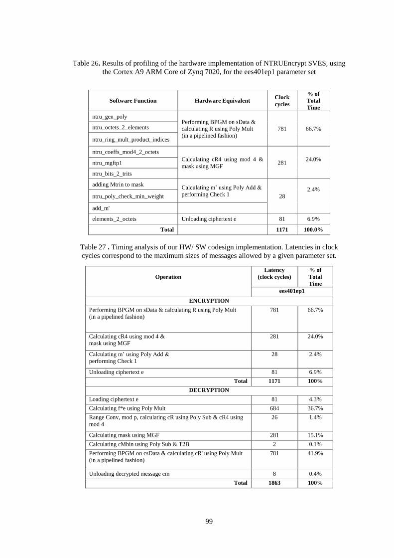
99
Table 26. Results of profiling of the hardware implementation of NTRUEncrypt SVES, using
the Cortex A9 ARM Core of Zynq 7020, for the ees401ep1 parameter set
Software Function Hardware Equivalent Clock
cycles
% of
Total
Time
ntru_gen_poly Performing BPGM on sData &
calculating R using Poly Mult
(in a pipelined fashion)
781 66.7% ntru_octets_2_elements
ntru_ring_mult_product_indices
ntru_coeffs_mod4_2_octets
Calculating cR4 using mod 4 &
mask using MGF 281
24.0%
ntru_mgftp1
ntru_bits_2_trits
adding Mtrin to mask Calculating m’ using Poly Add &
performing Check 1 28
2.4%
ntru_poly_check_min_weight
add_m'
elements_2_octets Unloading ciphertext e 81 6.9%
Total 1171 100.0%
Table 27 . Timing analysis of our HW/ SW codesign implementation. Latencies in clock
cycles correspond to the maximum sizes of messages allowed by a given parameter set.
Operation
Latency
(clock cycles)
% of
Total
Time
ees401ep1
ENCRYPTION
Performing BPGM on sData & calculating R using Poly Mult
(in a pipelined fashion)
781 66.7%
Calculating cR4 using mod 4 &
mask using MGF
281 24.0%
Calculating m’ using Poly Add &
performing Check 1
28 2.4%
Unloading ciphertext e 81 6.9%
Total 1171 100%
DECRYPTION
Loading ciphertext e 81 4.3%
Calculating f*e using Poly Mult 684 36.7%
Range Conv, mod p, calculating cR using Poly Sub & cR4 using
mod 4
26 1.4%
Calculating mask using MGF 281 15.1%
Calculating cMbin using Poly Sub & T2B 2 0.1%
Performing BPGM on csData & calculating cR' using Poly Mult
(in a pipelined fashion)
781 41.9%
Unloading decrypted message cm 8 0.4%
Total 1863 100%
100
6.6 Conclusion
In this chapter, we profiled or software code for NTRUEncrypt and studied different
options for partitioning the design. We implemented the design that was the best
balanced in terms of optimal partitioning. We implemented the design and performed
critical path analysis based on the timing analysis. The reports conclude that pipelining
the variable rotator inside polynomial multiplier will always help for any parameter set.
A completely balanced pipelined approach can double operating frequency of the
polynomial multiplier. Folding the polynomial multiplier helps more in case of larger
parameter sets but is less effective to reduce the area for smaller parameter sets. We were
able to obtain a speedup of 9x when we offload the polynomial multiplier to the FPGA
coprocessor. This indicates that we can achieve a substantial speedup using codesign
approach as compared to the pure software approach if we carefully partition the design
in a balanced way and then use techniques to parallelize and pipeline the design.
6.7 Future Work
We analyzed our design for balanced pipelining and offloaded polynomial multiplier to
the hardware coprocessor. We left the BPGM and MGF components on the software
side. In future, our design can be made more flexible so that we could choose between
different parameter sets on the run time. Similarly, we can incorporate ease of changing
the HASH function for BPGM/ MGF component.

101
7 CONCLUSIONS & FUTURE WORK
Based on our contributions discussed in the earlier chapters, we would like to provide
the reader with concluding remarks and directions for future work in this field of study.
Our primary focus was to facilitate the process of speeding up and benchmarking
implementations and as a result, ranking post-quantum public-key cryptosystems. The
upcoming NIST standard candidate evaluation process for PQC algorithms puts all
these algorithms in spotlight. The evaluation based on their performance and
applicability in both hardware and software platforms is of prime importance to move
forward with the process of standardization. Our design provides a valuable reference
for any future hardware implementers of PQC schemes. It also paves the way for fair
ranking through effective benchmarking of post-quantum cryptosystems. Our
motivation was to have one platform to explore the flexibility of software and
performance of hardware through HW/SW codesign-based approach. Our design also
supports a common hardware API which can be adopted for implementations of any
future post-quantum cryptosystems. For the design space exploration of flexibility vs.
performance, we have presented a novel HW/SW codesign approach that supports both
algorithmic and implementation level flexibility. For performance, different techniques
like pipelining and folding the hardware architecture were used. Due to the importance
of partitioning between hardware and software, we have thoroughly profiled and
examined our algorithms to achieve the best of both worlds. The results of our RSA
design show that balanced partitioning of a design between hardware and software may
seem challenging but it can support promising flexibility vs performance tradeoff.

102
Through our study based on NTRUEncrypt, our goal was to compare the hardware
implementations of NTRUEncrypt SVES at the same security level, using the same API,
from the point of view of the execution time, resource utilization, and speed-up vs.
software, as well as flexibility and scalability in terms of supporting multiple parameter
sets. The comparisons revealed that all reported results support only one operand size.
Only one scalable architecture is reported in literature. Our study on NTRU SVES
scheme reveals that it is not always sufficient to rely on software profiling. As the
hardware supports parallel execution of logic, in our case HW profiling of NTRU
revealed that execution time is dominated by hash functions. We propose both
architectural and algorithmic level improvements in the design of NTRU to overcome
this bottleneck of the design. These kinds of observations cannot be made if only
software profiling is performed.
PQC cryptosystems do not have HW/SW codesign-based implementations and
flexibility explored. Majority of the designs targeted only one or two aspects (operand
size, use of DSP units, multiple algorithmic schemes) of flexibility. Finally, through our
flexible HW/SW codesign-based approach, we extend and provide a generic model for
the evaluation of other PQC algorithms to incorporate architectural and algorithmic level
improvements through this interesting design technique. The use of a common interface
along with codesign-based approach to have quick evaluation and early estimates can be
valuable for the post-quantum cryptographic community in the entire process of
benchmarking and ranking these candidates.

103
7.1 Possibilities for Future Work
We highlight some noteworthy aspects through which our adopted design methodology
can potentially be extended in the future.
High-Level Synthesis to speed-up development and benchmarking:
Use of HLS is rather limited in the field of cryptography. However, researchers have
applied use of HLS in the hardware benchmarking efforts of AES [60] and SHA-3
finalists [61]. They were able to observe that HLS based designs can obtain the same
ranking of candidates as the RTL based designs with a small penalty in terms of area
and performance. The results to evaluation of candidates to the HASH function
competition SHA-3 were very promising and there was a very good correlation between
RTL and HLS result with much shorter development time. Currently, there is also work
done on the comparison of HLS and RTL based designs for CEASER competition.
Post-Quantum cryptosystems is relatively a new class of cryptosystems. Therefore,
there is no standard yet and as a result, multiple algorithms have been evaluated from
the point of view of efficiency in hardware and the current situation is similar to that of
cryptographic contest for the standardization of SHA-3 hash functions. HLS can help
in the ranking of candidates with results comparable to RTL with a relatively less
performance penalty. With the threat of post-quantum computers in near future, it is
important analyze to as many post-quantum resistant algorithm as possible. The
development time and comparable ranking obtained using HLS will be more beneficial
than having a smaller set of candidates evaluated using RTL in the same time frame.
Comparison of RTL and HLS based approaches in terms of development time,
execution time and area utilization can also be very beneficial.
104
Algorithmic and architectural level improvements in NTRU:
Our future work will involve taking advantage of any additional optimizations at the
algorithmic and hardware architecture levels. From the architectural aspect, we can
possibly explore the use of unrolled implementations of SHA-2, with two or more
rounds per clock cycle to remove the bottleneck in NTRU. To reduce the area we can
also fold the rotator inside the polynomial multiplier unit. At the algorithmic level, SHA-
3 can be adopted instead of SHA-2 or a pseudorandom function based on pipelined AES
can be used. We can also eliminating (or at least reducing) the dependence of the
execution time on message size.
Improvements in HW/SW Codesign-based approach
For NTRUEncrypt SVES, other partitioning schemes can be explored to even further
extend the evaluation process. For RSA, the extension could include implementing
other exponentiation algorithms. communication, computation overlap in design to
improve performance. Utilizing multiple high performance ports to reduce the number
of clock cycles for data communications can also be a possible future extension.
Resistance to Side-Channel Attacks:
As we implemented the NTRUEncrypt scheme published as the IEEE 1363.1 standard
specification, the careful choice of parameters is already adopted. Additionally, from the
security point of view, adding support for resistance against side-channel attacks by
introducing necessary countermeasures can also be explored for all implemented
schemes.
105
A. PUBLICATIONS
M.U. Sharif, R. Shahid, M. Rogawski, and K. Gaj, “Use of embedded FPGA resources in
implementations of five round three SHA-3 candidates”, May. 2011, ECRYPT II Hash
Workshop 2011
Maria Malik, Teng Li, Umar Sharif, Rabia Shahid, Tarek A. El-Ghazawi, and Gregory B.
Newby, Productivity of GPUs under diff erent programming paradigms,Concurrency and
Computation:Practice and Experience, Vol. 24, Nr. 2 (2012) , p. 179-191
R. Shahid, M.U. Sharif, M. Rogawski, and K. Gaj, “Use of embedded FPGA resources in
implementations of 14 Round 2 SHA-3 candidates”, The 2011 International Conference on
Field-Programmable Technology, FPT 2011, New Delhi, India, Dec. 12-14, 2011
K. Gaj, E. Homsirikamol, M. Rogawski, R. Shahid, and M.U. Sharif, “Comprehensive
Evaluation of High-Speed and Medium-Speed Implementations of Five SHA-3 Finalists Using
Xilinx and Altera FPGAs”, 3rd SHA-3 Candidate Conference, March. 22-23, 2012
M.U. Sharif, M. Rogawski, R. Shahid, and K. Gaj, “Hardware-Software Codesign of Pairing-
Based Cryptosystems for Optimal Performance vs. Flexibility Trade-off”, Proc. CryptArchi
2014, Annecy, France, June2014.
E. Homsirikamol, W. Diehl, A. Ferozpuri, F. Farahmand, M.U. Sharif, and K. Gaj, “Toward a
Universal High-Speed Interface for Authenticated Ciphers”, Proc. CryptArchi 2015, Leuven,
Belgium, June 2015.
E. Homsirikamol, W. Diehl, A. Ferozpuri, F. Farahmand, M.U. Sharif, K. Gaj, “GMU
Hardware API for Authenticated Ciphers”, Proc. DIAC 2015: Directions in Authenticated
Ciphers, Singapore, 27-29 Sep. 2015.
M. U. Sharif, R. Shahid, M. Rogawski, and K. Gaj,“Hardware-software codesign of RSA for
optimal performance vs. flexibility trade-off”, 26th International Conference on Field
Programmable Logic and Applications (FPL), Lausanne, Switzerland, Aug. 2016
M. U. Sharif, and K. Gaj, “Lessons Learned from High-Speed Implementation and
benchmarking of two Post-Quantum Public-Key Cryptosystems”, Cryptarchi 2017, Smolenice,
Slovakia, June. 2017
M. U. Sharif, and K. Gaj, “A Generic High-Speed and HW/SW Codesign Implementations of
NTRU Encrypt (SVES)”, International Conference on Reconfigurable Computing and FPGAs
(ReConfig 2017), Cancun, Mexico, Dec. 2017 (to be submitted)

106
BIBLIOGRAPHY
[1] M. E. H. Whitfield Diffie, "New Directions in Cryptography," IEEE Transactions on
Information Theory, vol. 22, no. 6, 1996.
[2] R. L. Rivest, A. Shamir and L. Adleman, "A method for obtaining digital signatures
and public-key cryptosystems," in Commun. ACM, 21(2), February 1978, pp 120– 126.
[3] P. W. Shor, "Polynomial-time algorithms for prime factorization and discrete
logarithms on a quantum computer," Journal on Computing, vol. 26, no. 5, p. 1484–
1509, 1997. .
[4] S. Kumar and C. Paar, "Reconfigurable Instruction Set Extension for Enabling ECC on
an 8-bit Processor," in 14th International Conference, FPL , Leuven, Belgium, 2004,
pp 586-595.
[5] G. Orlando and C. Paar, "A High-Performance Reconfigurable Elliptic Curve
Processor for GF(2m)," in Cryptographic Hardware and Embedded Systems,
Worcester, MA, 2000. pp 41-56.
[6] K. Sakiyama, L. Batina, B. Preneel and I. Verbauwhede, "HW/SW co-design for
accelerating public-key cryptosystems over GF(p) on the 8051 micro-controller," in
World Automation Congress (WAC), IEEE, 2006, pp 1–6.
[7] R. C. C. Cheung, W. Luk and P. Y. K. Cheung, "Reconfigurable Elliptic Curve
Cryptosystems on a Chip," in Design, Automation and Test in Europe - Volume 1 ,
Washington, DC, 2005. pp 24-29 .
[8] K. Saeedi1, S. Simmons2, J. Z. Salvail1, P. Dluhy1, H. Riemann3, N. V. Abrosimov3,
P. Becker4, H.-J. Pohl5, J. J. L. Morton6, M. L. W. Thewalt1 and *, "Room-
Temperature Quantum Bit Storage Exceeding 39 Minutes Using Ionized Donors in
Silicon-28," 2013.
[9] N. Gura, A. Patel, A. Wander, H. Eberle and S. C. Shantz, " Comparing elliptic curve
cryptography and RSA on 8-bit CPUs," in Cryptographic Hardware and Embedded
Systems, Cambridge, MA, 2004. pp. 119–132.
[10] L. Batina, D. Hwang, A. Hodjat, B. Preneel and I. Verbauwhede, "Hardware/Software
Co-design for Hyperelliptic Curve Cryptography (HECC) on the 8051 μP," in
Cryptographic Hardware and Embedded Systems, Edinburgh, UK, 2005. pp 106-118.
[11] D. Bernstein, J. Buchmann and E. Dahmen, "Post-Quantum Cryptography," Springer-
Verlag Berlin Heidelberg, 2009.
[12] M. Ajtai, "Generating hard instances of lattice problems," New York, NY, 1996.

107
[13] J. Hoffstein, J. Pipher and J. H. Silverman, "NTRU: A Ring-Based Public Key
Cryptosystem," in Proceedings of the Third International Symposium on Algorithmic
Number Theory , London, UK, 1998. pp 267-288 .
[14] IEEE Std P1363.1-2008, IEEE Standard Specification for Public Key Cryptographic
Techniques based on Hard problems over Lattices, March. 2009.
[15] "Financial Services Industry's Accredited Standards Committee X9, ANSI X9.98-
2010, Lattice-Based Polynomial Public Key Establishment Algorithm for the Finalcial
Services Industry," 2010.
[16] "Consortium for Efficient Embedded Security, Efficient Embedded Security Standards
(EESS), EESS #1: Implementation Aspects of NTRUEncrypt, v. 3.1," Sep. 2015.
[17] J. Schanck, W. Whyte and Z. Zhang, "Quantum-Safe Hybrid (QSH) Ciphersuite for
Transport Layer Security (TLS) version 1.3, TLS Working Group Internet Draft," Oct.
2016 (work in progress).
[18] L. Chen, Y. -K. Liu, S. Jordan, D. Moody, R. Peralta, R. Perlner and D. Smith-Tone,
"Report on Post-Quantum Cryptography," National Institute of Standards and
Technology Internal Report, NISTIR 8105 DRAFT, Feb. 2016.
[19] D. Moody, "Post-Quantum Cryptography: NIST's Plans for the Future," in 7th
International Conference on Post-Quantum Cryptography, PQCrypto 2016, Fukuota,
Japan, Feb. 24-26. 2016.
[20] "National Institute of Standards and Technology, Post-Quantum Crypto Project,"
[Online]. Available: http://csrc.nist.gov/groups/ST/post-quantum-crypto/.
[21] D. Suzuki, "How to maximize the potential of fpga resources for modular
exponentiation," in Proc. 9th International Workshop on Cryptographic Hardware in
Embedded Systems (CHES’07), Sep. 2007, pp. 272–288.
[22] P. L. Montgomery, "Modular multiplication without trial division," in Math. Comp.,
44(170), 1985, pp 519–521.
[23] H. Orup, "Simplifying quotient determination in high-radix modular multiplication," in
Proceedings of the 12th Symposium on Computer Arithmetic, Jul 1995, pp 193–199.
[24] M. Simka and V. Fischer, "Hardware-software codesign in embedded asymmetric
cryptography application - A case study," in Proc. Field-Programmable Logic and
Applications, 2003, pp 1075–1078.
[25] M. K. Hani, H. Wen and A. Paniandi, "Design and implementation of a private and
public key crypto processor for next generation IT security applications.," in
Malaysian J. Comput. Sci., 19, 2006, pp 29–45.
[26] M. Issad, B. Boudraa, M. Anane and N. Anane, "Software/hardware co-design of
modular exponentiation for efficient RSA cryptosystem," in Journal of Circuits,
Systems, and Computers, 23(3), 2014.
108
[27] L. Uhsadel, M. Ullrich, I. Verbauwhede and B. Preneel, "Interface design for mapping
a variety of RSA exponentiation algorithms on a HW/SW co-design platform.," in
Proceedings of the 2012 IEEE 23rd International Conference on Application-Specific
Systems, Architectures and Processors, ASAP ’12, Washington, DC, USA, 2012, pp
109–116.
[28] M. Koschuch, J. Lechner, A. Weitzer, J. Großschädl, A. Szekely, S. Tillich and J.
Wolkerstorfer, "Hardware/software co-design of elliptic curve cryptography on an
8051 microcontroller," in International conference on Cryptographic Hardware and
Embedded Systems , Berlin, Heidelberg, 2006. pp 430-444.
[29] C. P. L. Gouvêa, L. B. Oliveira and J. López, "Efficient software implementation of
public-key cryptography on sensor networks using the MSP430X microcontroller," in
Journal of Cryptographic Engineering, 2012, pp. 19–29.
[30] E. Wenger, T. Unterluggauer and M. Werner, 8/16/32 Shades of Elliptic Curve
Cryptography on Embedded Processors, Mumbai, India: INDOCRYPT , 2013.
[31] E. Wenger, "Hardware Architectures for MSP430-based Wireless Sensor Nodes
Performing Elliptic Curve Cryptography," in 11th International Conference, ACNS ,
Banff, AB, Canada, 2013, pp 290-306.
[32] J. Balasch, B. Gierlichs, K. Jaurvinen and I. Verbauwhede, "Hardware/software co-
design flavors of elliptic curve scalar multiplication," in IEEE International
Symposium on Electromagnetic Compatibility (EMC), Raleigh, NC , 2014 .
[33] M. Hassan, "A scalable hardware/software co-design for elliptic curve cryptography
on PicoBlaze microcontroller," in Proceedings of 2010 IEEE International Symposium
on Circuits and Systems (ISCAS), Paris, 2010.
[34] D. V. Bailey, D. Coffin, A. Elbirt, J. H. Silverman and A. D. Woodbury, "NTRU in
Constrained Devices," in Cryptographic Hardware and Embedded Systems , Paris,
France, 2001. pp 262-272.
[35] C. M. O. Rourke, "Efficient NTRU Implementations," MS Thesis, Worcester
Polytechnic Institute, 2006.
[36] J.-P. Kaps, "Cryptography for Ultra-Low Power Devices," PhD Thesis, Worcester
Polytechnic Institute, 2006.
[37] A. C. Atıcı, L. Batina, J. Fan, I. Verbauwhede and S. Yalcin, "Low-cost
Implementations of NTRU for pervasive security," in International Conference on
Application-Specific Systems, Architectures and Processors, ASAP, Leuven, 2008. pp
79 - 84 .
[38] A. Kamal and A. Youssef, "An FPGA implementation of the NTRUEncrypt
cryptosystem," in International Conference on Microelectronics (ICM), Marrakech,
2009. pp 209 - 212 .

109
[39] Ç. Koc, T. Acar and B. J. Kaliski, "Analyzing and comparing montgomery
multiplication algorithms," in IEEE Micro, 16(3), June 1996, pp 26–33.
[40] A. F. Tenca and C. K. Koc, "A scalable architecture for modular multiplication based
on montgomery’s algorithm," in IEEE Trans. Computers, 52(9), 2003, pp 1215–1221.
[41] D. Harris and K. Kelley, "Parallelized very high radix scalable montgomery
multipliers," in Proceedings of the 20th annual conference on Integrated circuits and
systems design, 2005, pp 306–311.
[42] M. Huang, K. Gaj and T. El Gazawi, "New hardware architectures for montgomery
modular multiplication algorithm," in Transactions on Computers, 2010.
[43] A. F. Tenca, R. F. Tenca, G. Todorov and C. K. Koc, "High-radix design of a scalable
modular multiplier," in Cryptographic Hardware and Embedded Systems — CHES
2001, 2001, pp 189–200.
[44] M. E. Kaihara and N. Takagi, "Bipartite Modular Multiplication Method," in IEEE
Trans. Computers 57(2): , 2008, pp 157-164.
[45] K. Sakiyama, M. Knežević and J. Fan, "Tripartite modular multiplication," in
Integration the VLSI Journal 09/2011; 44(4), 2011, pp 259-269.
[46] G. X. Yao, J. Fan, R. C. C. Cheung and I. Verbauwhede, "Faster Pairing Coprocessor
Architecture," in LNCS Volume 7708, 2013, pp 160-176.
[47] M. Rogawski, "Development and benchmarking of New Hardware Architectures for
Emerging Cryptographic Transformations, Ph.D. Thesis," George Mason University,
Fairfax, VA, 2013.
[48] D. F. Aranha and C. P. L. Gouvêa, "RELIC is an Efficient LIbrary for Cryptography,"
[Online]. Available: http://code.google.com/p/relic-toolkit/.
[49] I. San and N. At, "Improving the computational efficiency of modular operations for
embedded systems," in Journal of Systems Architecture - Embedded Systems Design,
60(5), 2014, pp 440-451.
[50] B. Song, K. Kawakami, K. Nakano and Y. Ito, "An rsa encryption hardware algorithm
using a single DSP block and a single block RAM on the FPGA," in IJNC, 1(2), 2011,
pp 277–289.
[51] Z. Wang, Z. Jia, L. Ju and R. Chen, "Asip-based design and implementation of RSA
for embedded systems," in Proceedings of the 2012 IEEE 14th International
Conference on High Performance Computing and Communication, 2012, pp 1375–
1382.
[52] A. Ferozpuri, F. Farahmand, M. U. Sharif, J. -P. Kaps and K. Gaj, "Hardware API for
Post-Quantum Public Key Cryptosystems," Technical Report, [Online]. Available:
https://cryptography.gmu.edu/athena/PQC/PQC_HW_API.pdf.
110
[53] "Cryptographic Engineering Research Group @ George Mason University, Source
Code for the SHA-3 Round 3 Candidates & SHA-2 - The Third SHA-3 Candidate
Conference Release," March. 2012. [Online]. Available:
https://cryptography.gmu.edu/athena/index.php?id=source_codes.
[54] "Security Innovation, Inc., Open Source NTRU Public key Cryptography Algorithm
and Reference code," [Online]. Available:
https://github.com/NTRUOpenSourceProject/ntru-crypto.
[55] B. Liu and H. Wu, "Efficient Multiplication Architecture over Truncated Polynomial
Ring for NTRUEncrypt System," in IEEE International Symposium on Circuits and
Systems, ISCAS 2016, Montreal, QC, Canada, 2016, pp 1174-1177.
[56] P. C. Kocher, "Timing Attacks on Implementations of Diffie-Hellman, RSA, DSS, and
other Systems," in CRYPTO 1996, pp. 104-113.
[57] S. Gueron and F. Schlieker, "Software Optimizations of NTRUEncrypt for Modern
Processor Architectures," in S. Latifi (ed.), Information Technology New Generations,
Advances in Intelligent Systems and Computing 448, pp. 189-199.
[58] "Announcing the first SHA1 collision," [Online]. Available:
https://security.googleblog.com/2017/02/announcing-first-sha1-collision.html.
[59] R. Lien, T. Grembowski and K. Gaj, "A 1Gbit/s Partially Unrolled Architecture of
Hash Functions SHA-1 and SHA-512," in LNCS 2964, RSA Conference 2004
Cryptographer's Track, CT-RSA 2004, San Francisco, CA, Feb. 2004, pp 324-328.
[60] E. Homsirikamol, W. Diehl, A. Ferozpuri, F. Farahmand, M. U. Sharif and K. Gaj,
"GMU Hardware API for Authenticated Ciphers," 2015.
[61] E. Homsirikamol and K. Gaj, "Hardware Benchmarking of Cryptographic Algorithms
Using High-Level Synthesis Tools: The SHA-3 Contest Case Study," in Applied
Reconfigurable Computing, Bochum, Germany, 2015. pp 217-228.
[62] D. Harris, R. Krishnamurthy, M. Anders, S. Mathew and S. Hsu, "An improved unified
scalable radix-2 montgomery multiplier," in Computer Arithmetic, 2005.
[63] N. Nedjah and L. D. M. Mourelle, "Software/hardware co-design of efficient and
secure cryptographic hardware," in J. Unive. Comput. Sci., , 2005, pp 66–82.
[64] Z. Wang, Z. Jia, L. Ju and R. Chen, "Development and benchmarking of new hardware
architectures for emerging cryptographic transformations," Ph.D. Thesis. George
Mason University, July 2013.
[65] Z. Wang, Z. Jia, L. Ju and R. Chen, "Asip-based design and implementation of RSA
for embedded systems," HPCC-ICESS, IEEE Computer Society, 2012, pp 1375–1382.
[66] N. Koblitz, "Elliptic curve cryptosystems,," in Mathematics of Computation, Vol. 48,
1987. pp. 203–209..

111
[67] D. Bernstein, "Cost analysis of hash collisions: Will quantum computers make
SHARCS obsolete?," Proc. 4th Workshop on Special-purpose Hardware for Attacking
Cryptograhic Systems, Lausanne, Switzerland, Sep. 9-10, 2009.
[68] D. Bernstein, "Introduction to post-quantum cryptography," [BBD09].
[69] D. Bernstein, "Grover vs. McEliece," Post-Quantum Cryptography, 2010.
[70] D. Buktu, "The NTRU Project," 2011. [Online]. Available:
http://tbuktu.github.io/ntru/.
[71] D. J. Bernstein, "McBits: Fast Constant-Time Code-Based Cryptography," in Prof.
15th International Workshop, Santa Barbara, CA, USA, August 20-23, 2013.
[72] "eBACS: ECRYPT Benchmarking of Cryptographic Systems," [Online]. Available:
http://bench.cr.yp.to.
[73] A. Canteaut and N. Sendrier, "Cryptanalysis of the Original McEliece Cryptosystem,"
in INRIA, 1998.
[74] N. Göttert, T. Feller, M. Schneider, S. A. Huss and J. Buchmann, "On the design of
hardware building blocks for modern lattice-based encryption schemes," in Proc.
CHES, 2012.
[75] M. Heger, "Cryptographers Take on Quantum Computers," in IEEE Spectrum, January
2009.
[76] S. Heyse, "Code-Based Cryptography: Implementing the McEliece Scheme on
Reconfigurable Hardware," Diploma Thesis, Ruhr-University Bochum, 31 May 2009.
[77] T. Eisenbarth, T. Güneysu, S. Heyse and C. Paar, "MicroEliece: McEliece for
Embedded Devices," in Proc. CHES, 2009, pp. 49-64.
[78] S. Heyse, I. Maurich and T. Güneysu, "Smaller Keys for Code-based Cryptography:
QC-MDPC McEliece Implementations on Embedded Devices," in Proc. CHES 2013,
Santa Barbara, USA, August 20-23, 2013.
[79] "Hybrid McEliece," [Online]. Available: https://www.rocq.inria.fr/secret/MCE .
[80] "Q&A With Post-Quantum Computing Cryptography Researcher Jintai Ding," in
IEEE Spectrum, 2008.
[81] A. Kamal and A. Youssef, "An FPGA implementation of the NTRUEncrypt
cryptosystem," in International Conference on Microelectronics (ICM), 2009, pp. 209-
212.
[82] I. von Maurich and T. Güneysu, "Lightweight Code-based Cryptography: QC-MDPC
McEliece Encryption on Reconfigurable Devices," in Proc. DATE 2014, Dresden,
Germany, March 24-28, 2014.
112
[83] D. Micciancio, "The Geometry of Lattice Cryptography," in UCSDCSE, 16 Feb. 2012.
[84] D. Micciancio and O. Regev, "Lattice-Based Cryptography," in New York University
Courant Institute of Mathematical Sciences, 22 July 2008.
[85] J. Morgan, "Quantum Memory," in World Record' Smashed, BBC News, 14 Nov.
2013.
[86] "NTRU Encryption Toolkits and Libraries," [Online]. Available:
https://www.securityinnovation.com/products/encryption-libraries/ntru-crypto/ .
[87] "PQCrypto – Post-quantum cryptography workshop series," [Online]. Available:
http://pqcrypto.org .
[88] "NIST Workshop on Cybersecurity in a Post-Quantum World," [Online]. Available:
http://www.nist.gov/itl/csd/ct/post-quantum-crypto-workshop-2015.cfm .
[89] "Quo Vadis Cryptology 2011," [Online]. Available:
http://cryptography.gmu.edu/quovadis/ .
[90] S. Tang, H. Yi, J. Ding, H. Chen and G. Chen, "High-speed Hardware Implementation
of Rainbow Signature on FPGAs," in Proc. PQCrypt , 2011.
[91] "Xilinx Zynq-7000 Extensible Processing Platform," [Online]. Available:
http://www.xilinx.com/products/silicon-devices/epp/zynq-7000.
[92] J. Ho.ffstein, J. Pipher and J. H. Silverman, "A Ring Base Public Key Cryptosystem,"
in Algorithmic Number Theory (ANTS III), Lecture Notes in Computer Science,
volume 1423, Berlin, 1998, pp 267-288.
[93] G. Gaubatz, J.-P. Kaps, E. Ozturk and B. Sunar, "State of the art in ultra-low power
public key cryptography for wireless sensor networks," in Third IEEE International
Conference on Pervasive Computing and Communications Workshops, 2005. PerCom
2005 Workshops. , Kauai Island, HI, 2005.
[94] N. Nedjah and L. D. M. Mourelle, "Software/hardware co-design of efficient and
secure cryptographic hardware," in J. Unive. Comput. Sci., 2005. pp 66–82.
[95] P. Schaumont, A Practical Introduction to Hardware/Software Codesign, Blacksburg,
VA: Springer US, 2013.
[96] F. Hu, K. Wilhelm, M. Schab, M. Lukowiak, S. Radziszowski and Y. Xiao, "NTRU-
based Sensor Network Security: A Low-power Hardware Implementation
Perspective," International Journal of Security and Communication Networks (Wiley),
vol. 2, no. 1, pp. pp 71-81, 2009.
[97] T. Pöppelmann, L. Ducas and T. Güneysu, "Enhanced Lattice-Based Signatures on
Reconfigurable Hardware," in Cryptographic Hardware and Embedded Systems,
Busan, South Korea, 2014. pp 353-370.
113
[98] T. Pöppelmann and T. Güneysu, "Towards Practical Lattice-Based Public-Key
Encryption on Reconfigurable Hardware," in Selected Areas in Cryptography - SAC ,
Burnaby, BC, Canada, 2013. pp 68-85.
[99] S. S. Roy, F. Vercauteren, N. Mentens, D. D. Chen and I. Verbauwhede, "Compact
Ring-LWE Cryptoprocessor," in Cryptographic Hardware and Embedded Systems,
Busan, South Korea, 2014. pp 371-391.
[100] O. Regev, "On lattices, learning with errors, random linear codes, and cryptography,"
in ACM symposium on Theory of computing , New York, NY, 2005. pp 84-93 .
[101] E. Homsirikamol and K. Gaj, "Can High-Level Synthesis Compete Against a Hand-
Written Code in the Cryptographic Domain? A Case Study," in International
Conference on ReConFigurable Computing and FPGAs (ReConFig), Cancún, Mexico,
2014.
[102] E. Homsirikamol, W. Diehl, A. Ferozpuri, F. Farahmand and K. . . . Gaj, "C vs.
VHDL: Comparing Performance of CAESAR Candidates Using High-Level Synthesis
on Xilinx and Altera FPGAs," Cryptographic architectures embedded in
reconfigurable devices (CryptArchi), Leuven, Belgium, 2015.
[103] E. Homsirikamol and K. Gaj, "Hardware Benchmarking of Cryptographic Algorithms
Using High-Level Synthesis Tools: The SHA-3 Contest Case Study," Applied
Reconfigurable Computing (ARC), Bochum, Germany, 2015.
[104] E. Homsirikamol and K. Gaj, "Benchmarking of Cryptographic Algorithms in
Hardware," Directions in Authenticated Ciphers (DIAC), Santa Barbara, USA, 2014.
[105] L. H. Crockett, R. A. Elliot, M. A. Enderwitz and R. W. Stewart, The Zynq Book,
Glasgow, Scotland, UK: Strathclyde Academic Media, 2014.
[106] Financial Services Industry's Accredited Standards Committee X9, ANSI X9.98-2010,
Lattice-Based Polynomial Key Establishment Algorithm for the Financial Services
Industry, 2010.
[107] Consortium for Efficient Embedded Security, Efficient Embedded Security Standards
(EESS), eess #1: Implementation Aspects of NTRUEncrypt, v. 3.1, , Sep. 2015.
[108] B. Liu, "Efficient architectureand Implementation for NTRU Based Systems," Master's
Thesis, University of Windsor, Windsor, Ontario, Canada, Aug. 2015.
[109] B. Liu and H. Wu, "Efficient Architecture and Implementation for NTRUEncrypt
System," in IEEE 58th International Midwest Symposium on Circuits and Systems
(MWSCAS), Fort Collins, CO, Aug. 2015, pp 1-4.
[110] K. Wilhelm, "Aspects of Hardware Methodologies for the NTRU Public Key
Cryptosystem," Master's Thesis, RIT, Feb. 2008.
[111] F. Hu, Q. Hao, M. Lukowiak, Q. Sun, K. Wilhelm, S. Radziszowski and Y. Wu,
"Trustworthy Data Collection From Implantable Medical Devices Via High-Speed
114
Security Implementation Based on IEEE 1363," in IEEE Trans. Information
Technology in Biomedicine, vol. 14, no. 6, 2010, pp 1397-1404.
[112] "SHA-3 Contest," [Online]. Available:
http://csrc.nist.gov/groups/ST/hash/sha3/index.html.
[113] "SHA-3 Zoo," [Online]. Available: http://ehash.iaik.tugraz.at/wiki/The_SHA-3_Zoo.
[114] "SHA-3 Zoo: SHA-3 hardware implementations," [Online]. Available:
http://ehash.iaik.tugraz.at/wiki/SHA3_Hardware_Implementations.
[115] "ATHENa Project Website," [Online]. Available: http://cryptography.gmu.edu/athena.
[116] K. Gaj, J. Kaps, V. Amirineni, M. Rogawski, E. Homsirikamol and B. Brewster,
"ATHENa Automated Tool for Hardware EvaluatioN: Toward Fair and
Comprehensive Benchmarking of Cryptographic Hardware using FPGAs," in Proc.
20th Int. Conf. on Field Programmable Logic and Applications, FPL, Milan, Italy,
2010.
[117] K. Gaj, E. Homsirikamol and M. Rogawski, "Fair and Comprehensive Methodology
for Comparing Hardware Performance of Fourteen Round Two SHA-3 Candidates
Using FPGAs," in Proc. CHES 2010, Santa Barbara, CA, USA, Aug. 2010, pp. 264-
278.
[118] E. Homsirikamol, W. Diehl, A. Ferozpuri, F. Farahmand, M. U. Sharif and K. Gaj,
"GMU Hardware API for Authenticated Ciphers," 2015.
[119] E. Homsirikamol and K. Gaj, "Hardware Benchmarking of Cryptographic Algorithms
Using High-Level Synthesis Tools: The SHA-3 Contest Case Study," in Applied
Reconfigurable Computing, Bochum, Germany, 2015, pp 217-228.

115
BIOGRAPHY
Malik Umar Sharif received his Master of Science degree from George Washington
University, Washington, DC, in 2010. He received his Bachelor of Science from
National University of Sciences and Technology, Pakistan in 2001. During his Ph.D.
degree, he worked as a teaching assistant in the ECE department at GMU for several
years. During his work at GMU, he was also working towards his Ph.D. in Computer
Engineering from George Mason University, Fairfax, VA. Being a member of
Cyptographic Engineering Research Group (CERG), he worked on several projects
related to symmetric key and public key cryptosystems. His major research interests
include hardware security, software/hardware codesign and post-quantum public key
cryptosystems.