functionalization of buckled graphene
TRANSCRIPT
Graduate Theses, Dissertations, and Problem Reports
2011
Functionalization of Buckled Graphene Functionalization of Buckled Graphene
Timothy C. Nelson West Virginia University
Follow this and additional works at: https://researchrepository.wvu.edu/etd
Recommended Citation Recommended Citation Nelson, Timothy C., "Functionalization of Buckled Graphene" (2011). Graduate Theses, Dissertations, and Problem Reports. 2223. https://researchrepository.wvu.edu/etd/2223
This Thesis is protected by copyright and/or related rights. It has been brought to you by the The Research Repository @ WVU with permission from the rights-holder(s). You are free to use this Thesis in any way that is permitted by the copyright and related rights legislation that applies to your use. For other uses you must obtain permission from the rights-holder(s) directly, unless additional rights are indicated by a Creative Commons license in the record and/ or on the work itself. This Thesis has been accepted for inclusion in WVU Graduate Theses, Dissertations, and Problem Reports collection by an authorized administrator of The Research Repository @ WVU. For more information, please contact [email protected].

Functionalization of Buckled Graphene
Timothy C. Nelson
Thesis
Submitted to the
College of Engineering and Mineral Resources
at West Virginia University
in partial fulfillment of the requirements
for the degree of
Master of Science in Engineering
Dr. C.D. Stinespring, Chair
Dr. R.S. Hissam
Dr. John W. Zondlo
Department of Chemical Engineering
Morgantown, West Virginia
2011
Keywords: Graphene, Functionalization, Surface Chemistry, Bio-Sensor
ABSTRACT
Buckled graphene produced by the halogen based etching of 6H-SiC provides a new route for the functionalization
of the graphene surface. This surface provides an important new stepping off point in the development of
molecular electronics and sensors. While the graphene surface is relatively inert, the fluorinated defect sites
inherent in the buckled graphene surface yield an excellent location for chemical reactions such as nucleophilic
substitution. This thesis shows the utility of the fluorinated defect sites through the well characterized diazonium
reaction.
Buckled graphene films were prepared on silicon carbide substrates using inductively coupled plasma and reactive
ion etching, and annealed at 1000º C to coalesce the BG. The films were reacted with benzene, nitrobenzene,
acetonitrile, or a nitrophenyl diazonium salt solution. The diazonium salt was chosen due to its known reaction
with graphene produced by other methods. Consequently, reaction of the diazonium with buckled graphene would
provide a basis for comparing the reactivity of the surface with these other forums of graphene. The interactions
of buckled graphene with the other species were investigated as they represent either constituent parts of the
diazonium salt or the solvent. The reacted surfaces were analyzed by X-ray photoelectron spectroscopy, which
reveals changes in the surface chemical state due to the functionalization of the buckled graphene by each species.
Each reaction yielded significant π-π bonding, while the diazonium salt reaction produced additional covalently
bonded phenyl groups on the buckled graphene surface. The covalent reaction site was shown to be the surface
fluorinated defect site. This observation illustrates the utility of the buckled graphene surface in the
functionalization of graphene. Moreover, it provides additional confirmation of the nature of the buckled
graphene surface.
Functionalization of Buckled Graphene
Timothy C. Nelson

iii
ACKNOWLEDGEMENTS
I have many to thank as I finish this work in West Virginia. First, though, I must acknowledge
my wife, Kate Nelson, for all the support she gave throughout this time in our lives. I truly
would not be here without her love and efforts, and I am immensely grateful and thankful for all
she endured in this period.
My advisor, Dr. Charter D. Stinespring led me to and through this project. His expertise in this
area of my interests and experience vastly aided my growing understanding of the research of his
laboratory.
My committee Dr. Robin Hissam and Dr. John Zondlo worked quickly to review and aid my
research capabilities.
My labmates, Tobias Denig and Srikanth Raghavan spent many hours sharing their knowledge
and know-how to help out the new guy in the lab. I lean on their research and the many lab
discussions.
The Chemical Engineering department enjoys the help of two ladies, Bonnie Hemlock and Linda
Rogers. Both dropped whatever they were doing to help me more times than I wish to admit,
and I am very grateful for all of their help.
I thank the undergraduate class of 2009, and the straggler left behind. I didn‟t know what I was
getting into, and your help my „junior year‟ was greatly appreciated. And to the straggler, thanks
for the all the fun in the woods while I was left straggling behind.
I thank my good friends; for the talk and understanding and a chance to escape. And I thank the
growing understanding of my son, Loki. Loki, I am very excited to return to being your full-time
daddy, if you don‟t remember when last I was.
Finally, I would like to thank the NASA – WV Space Grant Consortium and the WVU –
Program to Stimulate Competitive Research for funding this project.

iv
TABLE OF CONTENTS
TITLE PAGE i
ABSTRACT ii
ACKNOWLEDGEMENTS iv
TABLE OF CONTENTS v
TABLE OF FIGURES/TABLES vii
CHAPTER 1: BACKGROUND AND INITIAL PROBLEM STATEMENT 1
CHAPTER 2: LITERATURE REVIEW
2.1 Preparation and Characterization of Graphene 6
2.2 Synthesis Research at WVU 7
2.3 Doping and Surface Functionalization 10
CHAPTER 3: EXPERIMENTAL METHODS
3.1 Sample Preparation 15
3.2 X-Ray Photoelectron Spectroscopy 16
CHAPTER 4: EXPERIMENTAL RESULTS AND DISCUSSION
4.1 The Buckled Graphene Surface 18
4.2 Adsorption of Benzene 19
4.3 Adsorption of Nitrobenzene 21
4.4 Adsorption of Acetonitrile 23
4.5 Adsorption of Nitrobenzenediazonium Tetrafluoroborate 26
4.6 Implications of this Research 28
CHAPTER 5: CONCLUSIONS

v
5.1 Conclusions 30
5.2 Future Work 34
REFERENCES 35

vi
List of Figures
Figure 1.1 The first Brillioun zone and carrier population of graphene 2
Figure 2.1 Optical and AFM images of graphene flakes 6
Figure 2.2 XPS spectra of plasma processed silicon carbide 8
Figure 2.3 XPS and surface sensitive fluorine spectra of buckled graphene 8
Figure 2.4 Schematic of the buckling of graphene 9
Figure 2.5 RHEED of SiC and buckled graphene 10
Figure 2.6 Reciprocal lattices of SiC and Graphite 10
Figure 2.7 Surface doping of diamond 11
Figure 2.8 F4-TCNQ on graphene 12
Figure 2.9 The diazonium reaction on graphene 13
Figure 2.10 Schematics of SN1 and SN2 reactions 14
Figure 3.1 Schematic of ICP/RIE etching process 15
Figure 3.2 Principle of X-ray photoelectron spectroscopy 16
Figure 4.1 C1s XPS of buckled graphene 18
Figure 4.2 F1s XPS of buckled graphene 19
Figure 4.3 C1s XPS of the benzene reacted buckled graphene 19
Figure 4.4 F1s XPS of the benzene reacted buckled graphene 20
Figure 4.5 C1s XPS of the nitrobenzene reacted buckled graphene 21
Figure 4.6 F1s XPS of the nitrobenzene reacted buckled graphene 22
Figure 4.7 N1s XPS of the nitrobenzene reacted buckled graphene 23
Figure 4.8 C1s XPS of the acetonitrile reacted buckled graphene 24
Figure 4.9 F1s XPS of the acetonitrile reacted buckled graphene 24

vii
Figure 4.10 N1s XPS of the acetonitrile reacted buckled graphene 25
Figure 4.11 C1s XPS of the diazonium reacted buckled graphene 26
Figure 4.12 F1s XPS of the diazonium reacted buckled graphene 26
Figure 4.13 N1s XPS of the diazonium reacted buckled graphene 27
1
CHAPTER 1
BACKGROUND AND PROBLEM STATEMENT
Carbon takes several interesting allotropic forms including amorphous, diamond, and
graphite. Of these, graphite, the most stable, is a semi-metal used in many differing applications
including pencils, batteries, lubricants and steelmaking.1 Graphite consists of layers of carbon
sheets. The carbon of each sheet binds into hexagonal honeycomb rings with sigma bonds
forming the inter-atomic sp2-C bonds and π-bonds above and below the plane forming the p-
orbitals. Sheets are bound together using van der Waals-like forces.2
Peierls and Landau3,4
deemed the separation of individual sheets of graphite a physical
impossibility in 1935 and 1937. At the time, experimental evidence suggested that all
monolayers yield to thermal fluctuations and inter-atomic forces. Put simply, they either fall
apart or “glom” together, but do not form monolayers. As a result, physicists theorized on the
properties of monolayers without hope of seeing actual materials.
The first report of graphene came in 2004 by Geim et al.6 They reported the mechanical
exfoliation of graphene from bulk graphite, and provided a first look at the physical properties of
the material. The early samples showed high quality, high carrier mobility, and susceptibility to
the electric field effect. This first report started the growing interest in what most scientists
previously believed impossible. It is for this work that Geim and Novaslov recently received the
2010 Nobel Prize in Physics.7
Since its discovery, graphene has been proposed for use in a wide variety of applications
including molecular electronics as well as chemical- and bio-sensors. The development of such

2
devices depends critically on tuning the electrical properties of graphene by functionalizing its
surface with a variety of molecules.
Graphene is a gapless semiconductor with several interesting properties as illustrated in
Figure 1a. The first major observation is that the resting mass of the charge carriers is zero,
giving the speed of the carriers a linear relationship between the energies of the conduction and
valence bands with momentum. Such a relationship implies that the charge carriers travel at
constant velocity, the Fermi velocity, and allows use of the Dirac rather than the Schrödinger
equation. The second conclusion comes in part from the first. As all the carriers move at the
same speed and as they are
limited to two dimensions,
they have exceptionally long
mean free paths. The mean
free path of an electron or hole
is the average distance the
carrier travels before collision
with a second carrier. The
mean free path of a carrier depends on the size, number and relative velocities of carriers. The
mean free path of an electron in graphene is on the micrometer scale.2
The gapless semiconducting nature of graphene implies that the material is conductive at
any temperature above absolute zero due to the ballistic movement of electrons inside graphene.
That is to say that at any temperature above zero there will be electrons thermally excited to the
conduction band, which will travel without scattering at high velocity for relatively large
distances under an applied potential. None-the-less, like other semiconductors, it is desirable to
(a) (b)
Figure 1.1. a) The edge of the first Brillouin zone shows the gapless
meeting of the conduction and valence bands. b) A magnetic field
applied perpendicular to a graphene surface shifts the population up or
down. [ref. 2,5]

3
modify the number and type of charge carriers in graphene. For normal semiconductors this is
achieved by substituting dopant atoms of different atomic groups into the crystal structure. This
approach would create high levels of defects in the graphene monolayer and is not feasible.
While some research suggests the utilization of bipolar electric fields to switch from n to p-type
conductivity (Figure 1b) a second possibility is the use of surface dopants.8
Doping techniques
by functionalizing the surface present a new and viable doping technique for graphene.
The major foreseeable limitation in the evolution of graphene electronics concerns
graphene synthesis methods. To date most of the key results for graphene have been
demonstrated using mechanically exfoliated graphene flakes. Typically dimensions for these are
on the order of microns. Moreover, these flakes must be placed on an insulating substrate in
order to construct usable electronic devices. While some progress has been made using pick and
place methods,9 it is difficult to imagine a semiconductor industry based on such procedures.
In related research at West Virginia University, Raghavan has demonstrated the synthesis
of buckled graphene films using halogen-based plasma etching of 6H-SiC.10
In addition, Denig11
has demonstrated that that the buckled graphene films have an electrical conductivity comparable
to exfoliated graphene. Moreover, under fairly crude conditions, it has been shown that metal
contacts with low interfacial resistance can be produced. The significance of these results is that
graphene films of controlled thickness and excellent electrical properties can now be produced
on insulating substrates using scalable methods that are well understood by the electronics
industry. The next step in the development of the buckled graphene films is to demonstrate the
control of electrical properties by functionalizing the surface.
The focus of the research described in this thesis is the functionalization of the buckled
graphene surface by several molecular groups and the chemical characterization of the
4
functionalized surface. The electronic properties of the functionalized materials are left to future
research. Specifically, this investigation seeks to develop an understanding of the chemical
change of both the surface and adspecies that occur upon functionalization. Bekyarova et al.12
have shown that epitaxial graphene formed by evaporation of Si form 4H-SiC can be
functionalized using 4-nitrophenyl diazonium tetrafluoroborate. As a basis for comparing the
buckled graphene with “normal” graphene, the present study has used x-ray photoelectron
spectroscopy (XPS) to investigate the reaction of 4-nitrophenyl diazonium tetrafluoroborate with
the buckled graphene surface. To complement these studies and provide a broader understanding
of the adsorption of diazonium salt, benzene, nitrobenzene, and acetonitrile was also
investigated. Benzene and nitrobenzene were included as simpler molecules representative of
components of the chosen diazonium salt. Adsorption of acetonitrile was included since the
diazonium salt was dissolved in acetonitrile for the diazonium reaction.
In Chapter 2, the synthesis methods currently used to produce normal graphene are
reviewed, the plasma based method of producing buckled graphene is described, and the results
of doping and functionalization studies for normal graphene are summarized. In Chapter 3, the
experimental methods used in the present research are described, and in Chapter 4, the
experimental results are presented and discussed. Moreover, the implications of these results for
sensors and molecular electronics are given. Finally, in Chapter 5, conclusions and
recommendations for future work are given.
5
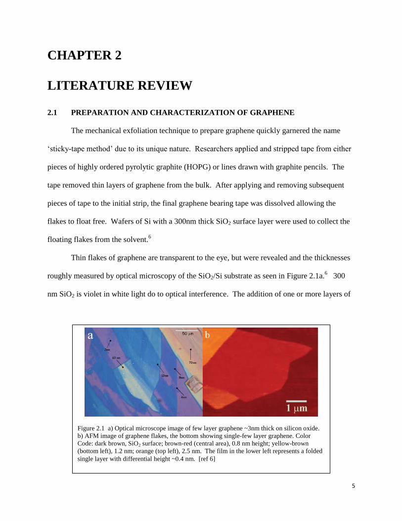
Figure 2.1 a) Optical microscope image of few layer graphene ~3nm thick on silicon oxide.
b) AFM image of graphene flakes, the bottom showing single-few layer graphene. Color
Code: dark brown, SiO2 surface; brown-red (central area), 0.8 nm height; yellow-brown
(bottom left), 1.2 nm; orange (top left), 2.5 nm. The film in the lower left represents a folded
single layer with differential height ~0.4 nm. [ref 6]
CHAPTER 2
LITERATURE REVIEW
2.1 PREPARATION AND CHARACTERIZATION OF GRAPHENE
The mechanical exfoliation technique to prepare graphene quickly garnered the name
„sticky-tape method‟ due to its unique nature. Researchers applied and stripped tape from either
pieces of highly ordered pyrolytic graphite (HOPG) or lines drawn with graphite pencils. The
tape removed thin layers of graphene from the bulk. After applying and removing subsequent
pieces of tape to the initial strip, the final graphene bearing tape was dissolved allowing the
flakes to float free. Wafers of Si with a 300nm thick SiO2 surface layer were used to collect the
floating flakes from the solvent.6
Thin flakes of graphene are transparent to the eye, but were revealed and the thicknesses
roughly measured by optical microscopy of the SiO2/Si substrate as seen in Figure 2.1a.6 300
nm SiO2 is violet in white light do to optical interference. The addition of one or more layers of

6
graphene to the optical path shifts the interference color to larger wavelengths (violet-blues to
blue) with increasing thickness. The thickness of graphene was further characterized by atomic
force microscopy (AFM). A typical AFM image of an un-exfoliated graphene flake is shown in
Figure 2.1b. Note that the flake has regions of varying thickness and it is only the small folded
region at the lower left which has monolayer thickness. In general such flakes are differentiated
into monolayer graphene, bi-layer graphene, and few layer graphene. At ten layers graphene
takes on the properties of bulk graphite.
The large numbers of applications for graphene demand a more robust method for the
preparation of graphene. This challenge has not been fully met, but several techniques under
current research show promise. Among these are chemical exfoliation and chemical vapor
deposition. Thermal annealing of SiC at temperatures between 1100 and 1500°C has also been
found to yield graphitic surface layers. Both the chemical exfoliation and CVD approach are
limited by the fact that the graphene must be transferred from a conducting growth substrate to a
nonconducting device substrate. The thermal approach produces graphene on an insulating SiC
substrate, but the process may be limited by the need to precisely control high annealing
temperatures over large areas for wafer scale production of graphene.
2.2 SYNTHESIS RESEARCH AT WVU
The graphene films used in this research were prepared using halogen based (CF4)
plasma etching to selectively etch Si from 6H-SiC (Cree Inc.). The resulting carbon-rich film is
annealed at 1000ºC. This reconstructs the surface to form the graphene film while desorbing all
but the most tightly bound halogens.

7
135 185 235 285
Binding Energy (eV)
No
rmalized
In
ten
sit
y
6H-SiC after HF Dip
C 1s
Si 2s
CF4 Etch: 100 W RIE / 400 W ICP
970 oC Anneal
0
200
400
600
800
1000
1200
1400
1600
1800
2000
279 284 289
Binding Energy (eV)
Inte
nsit
y (
cp
s)
C 1s Bulk
3 W
(a) (b)
Figure 2.2 a) XPS survey specta showing the Si 2s and C1s peaks for the 6H-SiC surface before and after plasma etching and annealing. b) C1s XPS spectra of the etched and annealed surface. [ref 10]
Figure 2.2a shows a portion of the x-ray photoelectric spectrum (XPS) for the surface
before and after the etching. Before the etching the intensities of the Si 2s and C 1s peaks are
indicative of stoichiometric SiC. After etching and annealing, the decrease in the Si2s intensity
relative to that of the C1s is indicative of the selective etching of Si.
Figure 2.2b shows the C 1s XPS peak for the etched and annealed surface. The peak at
282.5eV corresponds to the substrate. The peak at 284.1 eV corresponds to p-type graphene
(sp2-C). The peak at 285.7 eV corresponds to sp
2 C, which is denoted as CC. While the peak at
288.1 eV corresponds to sp3-C bound to an F atom and denoted as CF
39. The later three peaks are
all related to the graphene film. The ratio of the graphene related peaks to the substrate peak
reveals that this film is two to three layers thick.10
This is just slightly thicker than most films
produced under similar conditions.

8
Figure 2.3 shows F 1s spectra for this sample taken using bulk (a) and surface sensitive
(b) analysis modes. On going from bulk to surface sensitive mode, careful analysis show that the
peak at lower binding energy decreases in intensity relative to the higher binding energy peak.
This indicates that the lower binding energy peak is due to a sub-surface species while that at
higher binding energy is due to a surface species. These F species are both associated with the
CF species discussed in the context of the C1s spectrum. Recent experimental and computational
results have shown that the CF species is a unique specific defect in the graphene structure. 38
This defect is illustrated in figure 2.4a. It consists of two coupled sp3 hybridized C atoms each
bound to a F atom, one F atom is above the surface and other is below the surface.38
When
inserted into the sp2-C network, this defect produces a „buckled‟ graphene surface shown in
Figure 2.4b.38
It is this coupling of the sp3bonded C atoms which buckles the planer graphene
surface. The CC species is discussed in the context of the C1s spectra. In Figure 2.4a are sp2-C
atoms bound to these sp3-C atoms of the CF defect.
0
50
100
150
200
250
300
350
400
450
680 685 690
Binding Energy (eV)
Inte
ns
ity (
cp
s)
F 1s Bulk
3 W
0
20
40
60
80
100
120
140
160
180
680 685 690
Binding Energy (eV)
Inte
ns
ity (
cp
s)
F 1s Surface
3 W
(a) (b)
Figure 2.3. a) Bulk mode XPS of F1s peaks for buckled graphene film. b) Corresponding spectrum taken
in a surface sensitive analysis mode. [ref 10]

9
a. b.
Figure 2.4 a) The CF defect which consists of two coupled sp3-C atoms each
bound to an F atom with one F atom sitting above the surface and the other below
the surface. The sp3-C atoms bound to these sites are referred to as CC atoms. b)
A top down (above) and edge (below) view of the CF defect in the graphene
lattice. A major effect of this defect is to buckle the normally flat carbon plane.
Only one F atoms is visible in the top down view since the F atoms are situated
one above the other. [ref 38]
Figure 2.5
shows the reflection
high energy electron
diffraction (RHEED)
pattern for the buckled
graphene surface for
the 0011 azimuthal
direction.10
Patterns
for both the SiC
substrate and the
graphene overlayer
can be seen here.
Although this pattern
reveals a level of strain
in the graphene, it is very consistent with RHEED patterns
reported by Moreau40
for graphene produced by high
temperature annealing of SiC. It is not clear at this time if
the strain is due to the buckling of the surface or possibly
due to coupling to the substrate surface.
As a final note, Denig11
has measured the electrical
conductivity of these buckled graphene films using the
transmission line method. These results show that the
conductivity is a strong function of annealing temperature
Figure 2.5 a) RHEED pattern along the
0011 direction showing the spots due to
6H-SiC substrate (down arrows) and
additional spots due to the graphene overlayer
(up arrows). [ref 10]

10
and the number of graphene layers. In general, films similar to those used here have electrical
conductivities comparable to those of single layer exfoliated graphene films.
2.3 DOPING AND SURFACE FUNCTIONALIZATION
In conventional semiconductor materials, dopant atoms are incorporated as impurities
into crystal structures, randomly replacing atoms throughout the crystal or thin film. The
dopants typically differ in atomic group from the primary constituents and either have extra
electrons, which become free electrons, or are deficient in electrons and yield holes. The former
are classified as n-type semiconductors, while the latter are classified as p-type. While a typical
semiconductor is insulating, n-doped material contains filled energy levels very close to the edge
of the conduction band, resulting in a very easy transition to a conducting sample. P-doping
removes the highest energy electrons from the valence band and leaves holes as the majority
carrier in the material.
Surface doping differs in that dopants are not inserted into the crystal structure, but sit at
the surface as “solvated electrochemical species, isolated molecules, or solid adsorbates.”8 P-type
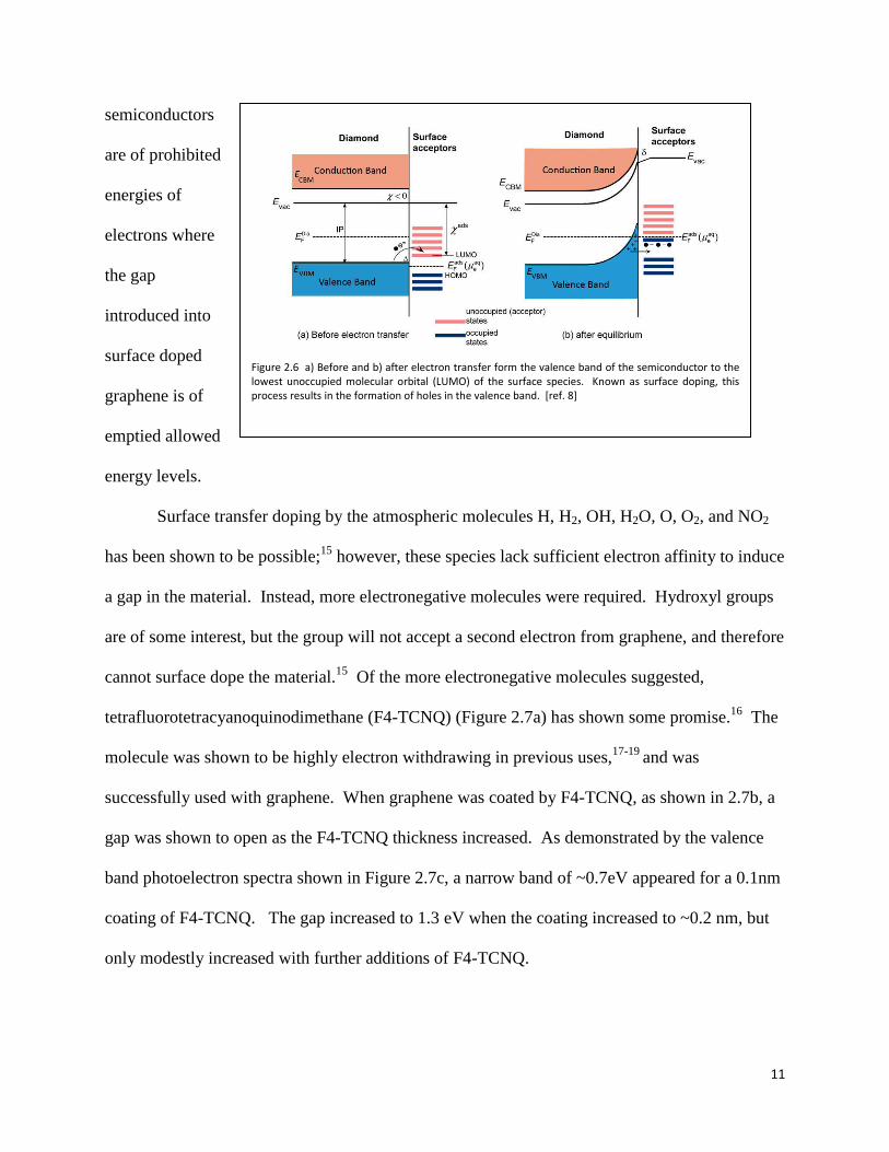
doping in this manner is most easily shown graphically as in Figure 2.6, where the lowest
unoccupied molecular orbital must be just above or beneath the valence band of the
semiconductor. In such a system, electrons from the valence band move to the lowest
unoccupied molecular orbital of the surface species. Figure 2.6 shows this process for diamond.
For graphene systems, the top of the valence band is at the Fermi level, and the removal of
electrons from the valence band results in an unfilled energy levels. The band gaps of traditional
11
Figure 2.6 a) Before and b) after electron transfer form the valence band of the semiconductor to the lowest unoccupied molecular orbital (LUMO) of the surface species. Known as surface doping, this process results in the formation of holes in the valence band. [ref. 8]
semiconductors
are of prohibited
energies of
electrons where
the gap
introduced into
surface doped
graphene is of
emptied allowed
energy levels.
Surface transfer doping by the atmospheric molecules H, H2, OH, H2O, O, O2, and NO2
has been shown to be possible;15
however, these species lack sufficient electron affinity to induce
a gap in the material. Instead, more electronegative molecules were required. Hydroxyl groups
are of some interest, but the group will not accept a second electron from graphene, and therefore
cannot surface dope the material.15
Of the more electronegative molecules suggested,
tetrafluorotetracyanoquinodimethane (F4-TCNQ) (Figure 2.7a) has shown some promise.16
The
molecule was shown to be highly electron withdrawing in previous uses,17-19
and was
successfully used with graphene. When graphene was coated by F4-TCNQ, as shown in 2.7b, a
gap was shown to open as the F4-TCNQ thickness increased. As demonstrated by the valence
band photoelectron spectra shown in Figure 2.7c, a narrow band of ~0.7eV appeared for a 0.1nm
coating of F4-TCNQ. The gap increased to 1.3 eV when the coating increased to ~0.2 nm, but
only modestly increased with further additions of F4-TCNQ.

12
Figure 2.7 a) The tetrafluorotetracyanoquinodimethane (F4-TCNQ) molecule. b) Schematic
of F4-TCNQ on graphene surface showing the layering of the molecule on the substrate. c)
Valence band photoelectron spectroscopy showing the formation of a 1.3 eV depletion region
in graphene‟s valence band by the electron withdrawal. [ref 16]
Although surface transfer doping offers proven doping ability, substitutional and covalent
reactions give different options. Sulfur substitution was computationally shown to induce a
0.3eV band gap in graphene by deformation of the graphene structure.20
The slightly longer
carbon-sulfur bonds cause the sulfur to rise a small distance above the surface, and this distortion
was thought to produce the small band gap. 20
A second computational study by the same group
looked at the cycloaddition of azomethine ylides to graphene.21
They reported that sp3
hybridized graphene would show a band gap, but that the ylides only react with graphene at the
Stone Wales defect sites, a combinational defect in graphene and carbon nanotubes in which one
ring contains only five carbons and an adjacent ring consists of seven.22

13
Figure 2.8 The diazonium reaction forms an out of plane bond to the phenyl group, producing nitrogen gas as a byproduct. [ref 12]
Another covalent reaction that creates a sp3 hybrized graphene and is suggested to yield a
band gap is the diazonium reaction. This process is illustrated in figure 2.8.12
This reaction is
frequently used to covalently attach phenyl groups to metals, silicon and graphitic materials.
Nitro-phenyl groups attached to graphene were shown to be chemically, electrically and
thermally stable. The resistivity of the reacted graphene was significantly increased by this
reaction.12
It is interesting to note that other R ground could be attached in this manner.
Bon, et al. prepared graphene by chemical exfoliation of graphite and then exposed the
graphene to a CF4 plasma to form sp3 hybridized carbon on the surface.
23 The fluorinated carbon
was then easily reacted with the nucleophilic amine group in butylamine. The fact that
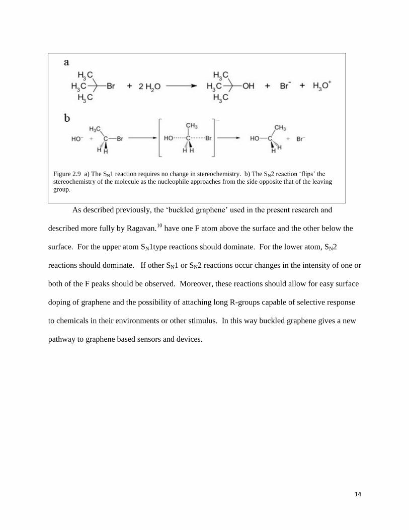
nucleophilic groups replace halides suggests either a SN1 or SN2 reaction. Figure 2.9 shows
examples of SN1 and SN2 type reactions. For SN1 reactions, no change in stereochemistry is
required. The SN2 reaction flips the stereochemistry of the molecule as the nucleophile enters
from the site opposite that of the exiting group.
14
Figure 2.9 a) The SN1 reaction requires no change in stereochemistry. b) The SN2 reaction „flips‟ the
stereochemistry of the molecule as the nucleophile approaches from the side opposite that of the leaving
group.
As described previously, the „buckled graphene‟ used in the present research and
described more fully by Ragavan.10
have one F atom above the surface and the other below the
surface. For the upper atom SN1type reactions should dominate. For the lower atom, SN2
reactions should dominate. If other SN1 or SN2 reactions occur changes in the intensity of one or
both of the F peaks should be observed. Moreover, these reactions should allow for easy surface
doping of graphene and the possibility of attaching long R-groups capable of selective response
to chemicals in their environments or other stimulus. In this way buckled graphene gives a new
pathway to graphene based sensors and devices.

15
Figure 3.1 The Trion Technology Phantom 3
ICP RIE utilizes two RF power sources: one to
generate a dense plasma and the second to
motivate the plasma to the sample surface for
reaction
CHAPTER 3
EXPERIMENTAL METHODS
3.1 SAMEPLE PREPARATION
As described in section 2.1, the buckled graphene films were 6H-SiC. . In the work
presented here, ICP-RIE was performed using a Trion Technology Phantom 3 ICP RIE with 300
W ICP and 400 W RIE power. A schematic of the process is shown in Figure 3.1. The process
was completed in 12 minutes at a pressure of 25 mTorr and a flow of 20 sccm of CF4. Four
pieces of 6H-SiC were attached to the center of a four
inch silicon wafer by carbon tape for each cycle. After
etching, the samples were annealed at 1000 º C under
ultrahigh vacuum conditions for 1hr to reconstruct the
carbon rich layer and form the buckled graphene film
The samples used in this study were supplied as
2inch wafers by Cree, Inc. and diced by American
Precision Dicing to half centimeter square pieces of
257 µm in thickness. Prior to the plasma process all
the SiC wafers were degreased in trichloroethylene, acetone and methyl alcohol.
Immediately after annealing, samples were removed from vacuum, and using a random
order, placed into vials of benzene (Aldrich anhydrous, 99.8%), nitrobenzene (Aldrich, 99.5%),
acetonitrile (Aldrich anhydrous, 99.8%) or a ten millimolar solution of 4 nitrobenzenediazonium
tetrafluoroborate (Aldrich, 97%) in acetonitrile. The vials were kept in the dark for twenty hours
before removal of the samples. Upon removal, the samples were washed with either benzene

16
Figure 3.2 Incident X-ray photons collide with and
displace inner electrons from the sample. The binding
energy of the level of the removed electron is then
calculated from the energy of the escaping electron,
the source photon and the instrument work function.
[ref 25]
(for the benzene and nitrobenzene adsorption) or acetonitrile (for the acetonitrile and diazonium
adsorption) and dried. The samples were then loaded into the UHV system for XPS analysis.
3.2 X-RAY PHOTOELECTRON SPECTROSCOPY
X-ray photoelectron spectroscopy (XPS) was accomplished with a Physical Electronics
5700 XPS system. Surface sensitive spectra, however, were acquired using a Physical
Electronics VersaProbe 5000 system located in the WVU Shared Facilities. Both instruments
have standard (Al/Mg filaments) and monochromated (Al filament) sources. The
monochromated Al source having an energy of 1486.6 eV was used to obtain all spectrum
reported here. The system was calibrated
using the Au XXX line at 84.0 eV. Sample
charging, when it occurred, was taken into
account by aligning the C1s peak for the SiC
substrate at 282.5 eV.
XPS has been historically called
electron spectroscopy for chemical analysis
(ESCA) as the technique gives information on
both chemical (oxidation) state and atomic
composition of samples.25
In XPS,
monoenergetic photons of known energy (hν)
displace core electrons from atoms, molecules
or ions as shown in figure 3.1. The kinetic
energy of the displaced electron (Ek) is

17
measured by the spectrometer and the electron‟s binding energy (Eb) is calculated based on
conservation of energy, using the equation:
Here, w is the work function of the spectrometer, which is taken into account during calibration
of the changes in the instrument. Changes in chemical state of the atoms produce small shifts on
the binding energies. These so called chemical shifts are well documented in the literature and
used extensively in the present work.

18
Figure 4.1 C 1s XPS spectrum representative of the buckled graphene surfaces used in these studies.
CHAPTER 4
EXPERIMENTAL RESULTS AND DISCUSSION
4.1 THE PREPARED BUCKLED GRAPHENE SURFACE
Figure 4.1 shows the C 1s XPS
peak for a CF4 etched 6H-SiC surface. In
this case, the etch conditions were 400 W
RIE, 300 W ICP, 25 mTorr and 20 sccm
of CF4 for 12 minutes. Similar conditions
were used for all samples in this study.
Deconvolution of this spectrum yielded
four peaks at 282.5 eV, 283.8 eV, 284.8
eV and 287.9 eV. The 282.5 eV peak is
tied to carbon in the SiC substrate.27
The
peak at 283.8 eV corresponds with sp2-C
in p-doped graphene as shown by the F4-TCNQ p-doped graphene studied by Chen.16
The last
two peaks originate in the p-doping of the material by fluorine as suggested by the experimental
and computational studies reported by Sato.28
Specifically, the peak at 287.9 eV corresponds to
the sp3 C atoms bound to F atoms and previously identified as CF species (see Figure 2.4).
Likewise, the peak at 284.8 eV corresponds to sp2-C atoms bound to the sp
3-C atoms and
previously identified as CC species.
Figure 4.2 shows the corresponding F 1s spectra which reveals two peaks, one at 685.0
eV and the other at 688.5eV. These species are the result of the plasma process and correspond
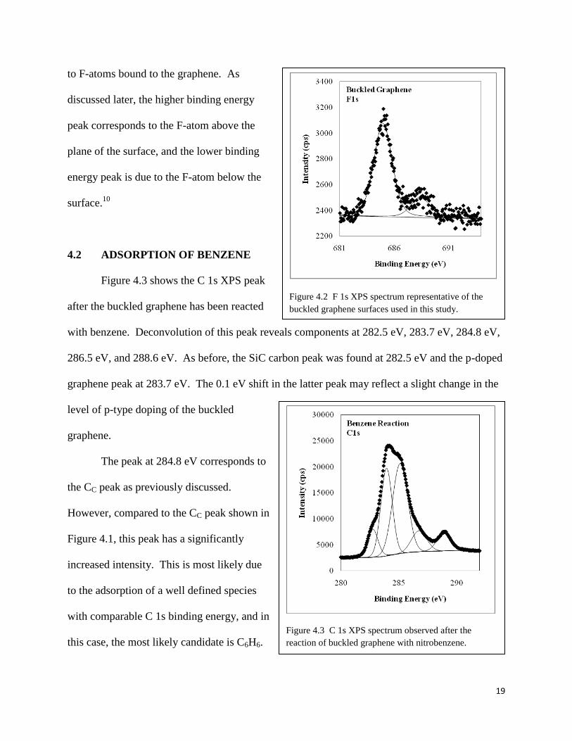
19
to F-atoms bound to the graphene. As
discussed later, the higher binding energy
peak corresponds to the F-atom above the
plane of the surface, and the lower binding
energy peak is due to the F-atom below the
surface.10
4.2 ADSORPTION OF BENZENE
Figure 4.3 shows the C 1s XPS peak
after the buckled graphene has been reacted
with benzene. Deconvolution of this peak reveals components at 282.5 eV, 283.7 eV, 284.8 eV,
286.5 eV, and 288.6 eV. As before, the SiC carbon peak was found at 282.5 eV and the p-doped
graphene peak at 283.7 eV. The 0.1 eV shift in the latter peak may reflect a slight change in the
level of p-type doping of the buckled
graphene.
The peak at 284.8 eV corresponds to
the CC peak as previously discussed.
However, compared to the CC peak shown in
Figure 4.1, this peak has a significantly
increased intensity. This is most likely due
to the adsorption of a well defined species
with comparable C 1s binding energy, and in
this case, the most likely candidate is C6H6.
Figure 4.3 C 1s XPS spectrum observed after the
reaction of buckled graphene with nitrobenzene.
Figure 4.2 F 1s XPS spectrum representative of the
buckled graphene surfaces used in this study.
20
Briggs and Seah29
place the C6H6 peak at 284.7 eV. This is in reasonable agreement with our
peak at 284.8 eV. In this case, the interaction of the C6H6 with the buckled graphene surface
most likely involves π-π stacking. That is, an interaction between the π-electrons of the ring and
the buckled graphene surface.
The peak at 286.5 eV may correspond to C6H5F. As noted by Sundberg and coworkers,30
fluorobenzene has a C 1s peak nominally in this position. In this case, the ring would lie in a
plane normal to the surface.
The peak at 288.6 eV may correspond to C6F6. Wagner et al.31
indicate that the C 1s
peak for this species is at 288.3 eV, which would be a reasonable match. Although it is tempting
to make this assignment, it is difficult to believe that there is enough mobility for adsorbed C6H6
molecules to scavenge F-atoms in this way. An alternative and more likely species is C=O.
Romaschin et al.32
place the C 1s for this species at 288.5 eV, which is in reasonable agreement
with our peak at 288.6 eV. A similar species was observed by Bekyarova et al.12
in their studies
of nitrophenyl diazonium adsorbed on graphene; although they place the peak at slightly lower
binding energy.
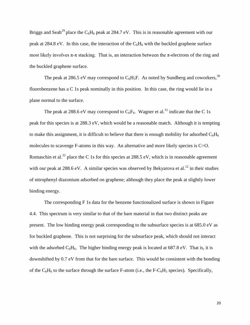
The corresponding F 1s data for the benzene functionalized surface is shown in Figure
4.4. This spectrum is very similar to that of the bare material in that two distinct peaks are
present. The low binding energy peak corresponding to the subsurface species is at 685.0 eV as
for buckled graphene. This is not surprising for the subsurface peak, which should not interact
with the adsorbed C6H6. The higher binding energy peak is located at 687.8 eV. That is, it is
downshifted by 0.7 eV from that for the bare surface. This would be consistent with the bonding
of the C6H6 to the surface through the surface F-atom (i.e., the F-C6H5 species). Specifically,
21
Figure 4.5 C 1s XPS spectrum observed after the reaction of
buckled graphene with nitrobenzene.
since this F-atom can draw charge from
both the underlying CF and C6H5 surface
moiety this added electronic charge should
act to lower the binding energy of the F 1s
peak.
In summary, it appears that the
benzene interacts with the buckled
graphene surface through π-π stacking (i.e.,
the C 1s peak at 284.8 eV) and also by
forming a bond with the surface F species.
(i.e., the C 1s peaks at 286.5 eV). Of these
two surface species, the latter is unique to buckled graphene, while the former might readily be
observed on exfoliated graphene. The origin of the C=O species (i.e., the C 1s peak at 288.6 eV)
is not clear.
4.3 NITROBENZENE
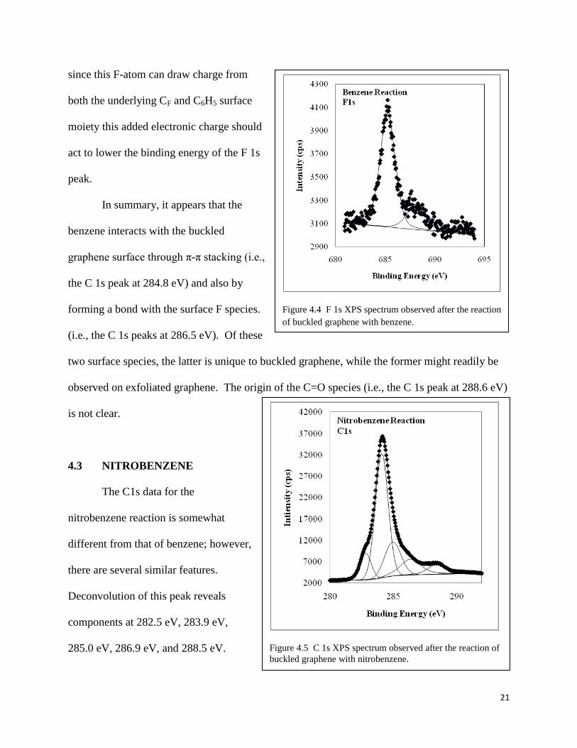
The C1s data for the
nitrobenzene reaction is somewhat
different from that of benzene; however,
there are several similar features.
Deconvolution of this peak reveals
components at 282.5 eV, 283.9 eV,
285.0 eV, 286.9 eV, and 288.5 eV.
Figure 4.4 F 1s XPS spectrum observed after the reaction
of buckled graphene with benzene.

22
Figure 4.6 F 1s XPS spectrum observed after the reaction of
buckled graphene with nitrobenzene.
Peaks for SiC and graphene again are found at 282.5 eV and 283.9 eV. The small (0.1 eV) up
shift in the graphene peak at 283.9 eV could simply mean a slight change in the level of p-type
doping.
The peak at 285.0 eV can again be attributed again to the overlap of the CC species and π-
π stacking interaction of the graphene with the adsorbed C6H5NO2 ring of the nitrobenzene
molecule. The peak at 286.9 eV can not be readily identified from standard spectra. The natural
assignment would be for the C-NO2 in the nitrobenzene, but the C 1s peak for this species
nominally occurs at 285.9 eV.31
Bekyarova et al.12
suggest that the NO2 in nitrobenzene is
reduced to NH2 by x-ray irradiation, but even in this case, the C-NH2 moiety has a C 1s peak also
in the range of 285.9 eV,31
so this does not seem to be a possibility. A third possibility is that
this peak corresponds to the nitrobenzene bound to the surface through the surface F-atom. This
would be similar to case for benzene (e.g., F-C6H4NO2 in this case) but with the C 1s peak up-
shifted by 0.4 eV. Of the three
possibilities the latter seems most
plausible. Results from the F 1s
spectrum discussed below are consistent
with this assignment. The peak at 288.5
eV, as in the case of benzene is most
likely due to C=O.
The F 1s spectrum for the
reaction of nitrobenzene is shown in
Figure 4.6. The lower binding energy
peak at 685.0 eV due to the subsurface
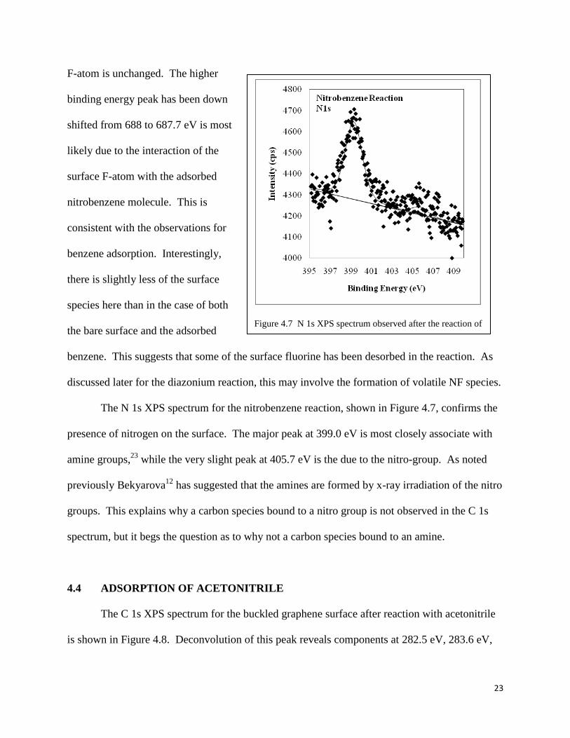
23
Figure 4.7 N 1s XPS spectrum observed after the reaction of
buckled graphene with nitrobenzene.
F-atom is unchanged. The higher
binding energy peak has been down
shifted from 688 to 687.7 eV is most
likely due to the interaction of the
surface F-atom with the adsorbed
nitrobenzene molecule. This is
consistent with the observations for
benzene adsorption. Interestingly,
there is slightly less of the surface
species here than in the case of both
the bare surface and the adsorbed
benzene. This suggests that some of the surface fluorine has been desorbed in the reaction. As
discussed later for the diazonium reaction, this may involve the formation of volatile NF species.
The N 1s XPS spectrum for the nitrobenzene reaction, shown in Figure 4.7, confirms the
presence of nitrogen on the surface. The major peak at 399.0 eV is most closely associate with
amine groups,23
while the very slight peak at 405.7 eV is the due to the nitro-group. As noted
previously Bekyarova12
has suggested that the amines are formed by x-ray irradiation of the nitro
groups. This explains why a carbon species bound to a nitro group is not observed in the C 1s
spectrum, but it begs the question as to why not a carbon species bound to an amine.
4.4 ADSORPTION OF ACETONITRILE
The C 1s XPS spectrum for the buckled graphene surface after reaction with acetonitrile
is shown in Figure 4.8. Deconvolution of this peak reveals components at 282.5 eV, 283.6 eV,

24
Figure 4.8 C 1s XPS sprctrum observed after the reaction of
buckled graphene with acetonitrile.
284.3 eV, 285.6 eV, and 288.1 eV. The
peaks at 282.5 eV and 283.6 eV are again
identified with the SiC substrate and the
p-doped graphene, respectively. In this
case, there is a 0.2 eV downshift in the
graphene peak which suggests an
increase in the level of p-doping. As will
be noted in the discussion of the F 1s
spectrum, the surface F level is higher on
this sample than even the bare surface
which would be consistent with the
suggested enhanced p-doping. In the
same way, the peak at 284.3 eV may be due to the CC species downshifted by 0.5 eV. The peak
at 285.6 eV is most likely due to a CN species.31
This is most likely the result of dissociative
chemisorption on the resultant covalent bonding of the nitrile group to the surface. Finally, the
C 1s peak at 288.1 is still most likely due to C=O species.
The F 1s spectrum for the acetonitrile reaction is shown in Figure 4.9. Again two peaks,
one at 684.9 eV and the other at 688.3 eV, are observed. These peaks are essentially the same as
those for the bare buckled graphene surface. As noted above, the surface fluorine peak is more
intense here than in the typical buckled graphene case, which suggests a higher level of p-doping
than usual. It appears that, in this case, somewhat less of the surface fluorine species were
desorbed during the thermal anneal. The fact that these peaks occur at their normal energies
suggests that the acetonitrile does not interact with the surface through the fluorine. This is

25
Figure 4.10 N 1s sprctrum observed after the reaction of
buckled graphene with acetonitrile.
Figure 4.9 F 1s XPS sprctrum observed after the reaction of
buckled graphene with acetonitrile.
distinctly different from the reactions for
benzene and nitrobenzene in which the
surface fluorine was involved in bonding
the benzene ring.
The N 1s spectrum for the
acetonitrile reaction is shown in Figure
4.10. For this spectrum only a single
peak at 399.1 eV is observed. This peak
is associated with the nitrile group,23
which is consistent with the CN moiety
at 285.6 eV in the C 1s spectrum.

26
Figure 4.12 F 1s XPS peak observed after the reaction of
buckled graphene with diazonium.
Figure 4.11 C 1s XPS spetrum observed after the reaction
of buckled graphene with diazonium. (may want to refit
this )
4.5 ADSORPTION OF NITROBENZENEDIAZONIUM TETRAFLUOROBORATE
Figure 4.11 shows the C1s
spectrum of the graphene following the
diazonium reaction. Deconvolution of
this peak reveals five components at
282.5 eV, 283.7 eV, 284.7 eV, 286.0 eV,
and 288.5 eV. These components and
the overall peak shape are very similar to
the case for benzene reaction. The SiC
and graphene peaks are located at 282.5
eV and 283.7 eV, respectively.
The C 1s peak at 284.7 eV
corresponds to the overlap of the CC and
π-π stacked C6H6 species as before. The
peak at 286.0 eV corresponds to the C-
NO2 or nitro species observed by
Bekyarova.12
It is not clear form XPS if
this is associated with the π-π stacked
C6H5NO2, or with a covalently bound C-
C6H4NO2. The infrared spectroscopy
results of Bekyarova12
suggest that
covalent bonding is the primary
attachment mode.
27
Figure 4.13 N 1s XPS peak observed after the reaction of
buckled graphene with diazonium.
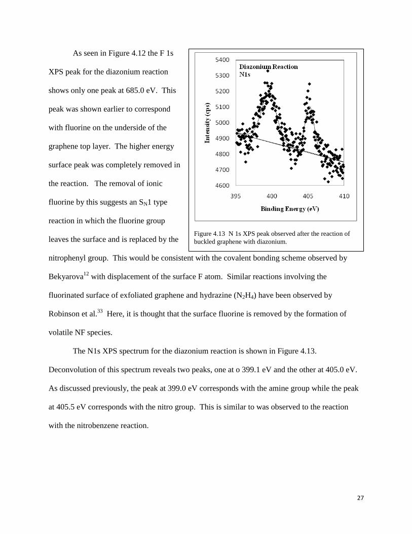
As seen in Figure 4.12 the F 1s
XPS peak for the diazonium reaction
shows only one peak at 685.0 eV. This
peak was shown earlier to correspond
with fluorine on the underside of the
graphene top layer. The higher energy
surface peak was completely removed in
the reaction. The removal of ionic
fluorine by this suggests an SN1 type
reaction in which the fluorine group
leaves the surface and is replaced by the
nitrophenyl group. This would be consistent with the covalent bonding scheme observed by
Bekyarova12
with displacement of the surface F atom. Similar reactions involving the
fluorinated surface of exfoliated graphene and hydrazine (N2H4) have been observed by
Robinson et al.33
Here, it is thought that the surface fluorine is removed by the formation of
volatile NF species.
The N1s XPS spectrum for the diazonium reaction is shown in Figure 4.13.
Deconvolution of this spectrum reveals two peaks, one at o 399.1 eV and the other at 405.0 eV.
As discussed previously, the peak at 399.0 eV corresponds with the amine group while the peak
at 405.5 eV corresponds with the nitro group. This is similar to was observed to the reaction
with the nitrobenzene reaction.

28
4.7 IMPLICATIONS OF THIS RESEARCH
The development of sensors and molecular electronics using buckled graphene produced
by the present synthesis method is dependent on several factors. The first of these relates to the
electrical properties of these films. In separate studies, Denig11
has shown that the buckled
graphene films have an electrical conductivity and carrier density comparable to exfoliated
graphene. Moreover, it has been shown that metal contacts with low interfacial resistance can be
produced. Thus, the first of the criteria has been met.
The second requirement is that the surface of buckled graphene can be functionalized.
This is necessary for both tailoring the doping levels of the film and for attaching molecules
which possess either biological activity, electrical conductivity, or other physical attributes. The
studies presented here represent a first step in demonstrating and characterizing the
functionalization of the buckled graphene surface.
It is interesting that as work for this thesis draws to a close, other groups are beginning to
look at fluorination of normal graphene surfaces as a means of opening “robust” pathways for
molecular additions.33
Thus the presence of these “defects” on the buckled graphene surface
may prove advantageous for functionalization processes. It is clear that halogens other than F
and Cl can be used (eg. Br)Frandlich
, and this may open a range of reaction pathways.
The results presented here have identified π-π stacking for benzene, nitrobenzene, and
diazonium. In addition, the possibility of a covalently bound C-C6H4NO2 species has been
observed in the case of diazonium interaction. The π-π interaction should be possible on both
buckled and exfoliated graphene. The covalent bond may require the displacement of the surface
F atom. In addition, we have observed bonds unique to the buckled graphene in the formation of
F-C6H5 covalent bonds for benzene and nitrobenzene.
29
The last example, that of the diazonium reaction, is the most promising due to the
displacement of F from the surface and the implications of the formation of a strong covalent
bonds. Similar reactions, such as the butyl amine reaction shown by Bon18
should be possible.
The importance of the diazonium reaction is two-fold. First this reaction presents a
pathway toward sensing materials and molecular electronics. Second, the removal of only the
high binding energy F 1s peak in the diazonium reaction corroborates the association of this peak
with the surface fluorine. The fact that the lower binding energy peak remained unchanged in all
reactions confirms its association with the subsurface fluorine. Taken together, these results for
the diazonium reaction substantially validate the buckled model of our graphene surfaces.
Finally, by inference from these results, it is possible to suggest strongly nucleophilic groups for
SN1 type reactions with the buckled graphene surface.

30
CHAPTER 5
CONCLUSIONS AND FUTURE WORK
5.1 CONCLUSIONS
The research presented here fills two purposes. The first is to aid in the characterization
of buckled graphene prepared by the plasma fluorination of SiC. The second is to functionalize
the surface of this new material. The latter is a critical first step in the development of chemical
and biochemical sensors as well as molecular electronics device structures using buckled
graphene. The basic approach uses XPS to characterize the bonding of 4-nitrobenzenediazonium
to the surface. In order to fully understand this interaction, it was necessary also investigate the
bonding of benzene, nitrobenzene, and acetonitrile to the buckled graphene surface. These
studies revealed the importance of several bonding modes including π-π van der Waals bonding
as well C(surface) -C and F(surface)-C covalent bonding of the benzene ring. Evidence
reflecting shifts in the level of p-type doping due to molecular attachment was observed. Finally,
it was observed that surface F atoms could be removed by the interaction of 4-nitrobenzene-
diazonium.
All adspecies containing the benzene ring exhibited π-π stacking as well as covalent
bonding to the surface the surface. For benzene and nitrobenzene, covalent bonding of the ring
through the surface F atom is observed. In this case the ring is normal to the surface rather than
parallel to the surface as is the case for π-π stacking. In the case of 4-nitrobenzenediazonium,
covalent bonding of the ring with a surface C atom and the elimination of the surface F atom is
observed. Again the ring should be normal to the surface in this configuration. This reaction is

31
also quite useful in confirming the assignment of the surface and subsurface XPS peaks and
thereby strengthening the spectroscopic characterization of the structure of the CC-CF defect.
The adsorption of 4-nitrobenzenediazonium and not nitrobenzene or benzene leads to
desorption of the surface fluorine. This is clear evidence of the importance of the diazo group in
removing the surface F atoms. This may have applications in both functionalizing the surface as
well as altering the doping level of the graphene film. As literature suggests, this reaction takes
place on graphene surfaces without the fluorine defect, however the complete removal of the out
of surface fluorine suggests the preferential reaction at this defect site.
A shift in the C 1s binding energy for the p-type graphene was observed after the
adsorption of each molecular species. As discussed, this suggests that the adsorption process
alters the doping of the film. This is critical if electrical properties are to be tailored.
The diazonium reaction in this research places a nitrophenyl group on the carbon surface,
which necessitated the additional trial of pure nitrobenzene with the buckled graphene. This test
gave results very similar benzene, but with and up shift in the binding energy of the C 1s
photoelectron. This directly relates to the electron withdrawing nitro group within the
nitrobenzene, and corresponds with literature reports. Nitrobenzene behaves very similarly to
benzene on the buckled graphene surface, which is understandable given the similar structure.
The importance of this data is, again, not the presence of nitrobenzene on the surface but the
difference between this spectrum and that following the diazonium reaction.
Acetonitrile was studied due to its role as the solvent of the diazonium salt. While future
studies may find a solvent which does not remain on the carbon surface, acetonitrile remains. It
causes a down shift in the C 1s peak for p-type graphene and the formation of residual nitrile
species on the surface.

32
The reaction with 4-nitrobenzenediazonium tetrafluoroborate was chosen in part due to
the recent study of the salt with thermally annealed graphene.12
The Bekyarova C1s post
reaction spectrum shows a broad peak at 285.57 eV, associated with the C-N bond within the
nitro-phenyl group, and a peak at 283.45 eV from newly p-doped graphene. This differs
significantly from the carbon spectra of this research; this difference is attributed to the buckled
graphene starting material. The graphene used by Bekyarova was not initially p-doped, and the
p-doping by the into-plane fluorine contributes significantly to the difference in the amount of
functionalization of the buckled graphene surface. The second contributing factor is the presence
of the out of plane F defect sites, which serve as reaction sites for the salt.
The diazonium reaction characterizes the buckled graphene surface beyond what was
done by surface sensitive XPS by the complete removal of only the higher binding energy F 1s
peak. This further identifies the carbons bound to fluorine as sp3 hybridized. While the sp
2
carbon of benzene, graphite and graphene is planer in structure, sp3 C assumes a tetragonal
structure to minimize the energy of the molecule. The energy of the structure is further reduced
by incorporating pairs of defects; out of surface F atoms pair with inter-planer F atoms.
The reaction at the out of surface fluoride site by the diazonium salt provides an excellent
pathway for the functionalization of graphene by molecules other than the nitrobenzene group.
First the reaction does not depend on the nitro group, which may be replaced by any R group.
An active R group may be reacted to the ring either before the attachment of the ring to the
graphene surface, or after. The nitro group was chosen due to ease of acquisition and relevant
recent research; however, other groups with more desirable reaction pathways should yield
similar results.
33
The reaction at the F defect supports the work of Bon, et al.,23
and begs the use of
nucleophilic groups to react this surface. That both the butylamine and diazonium salt reaction
favor the functionalization of the surface of the defect site proves the utility of this defect to
future research in the development of nanoscale sensors and molecular electronics. The
diazonium reaction is an important tool for the functionalization of graphene, but the fluorine
doping of the material outshines the salt by yielding greater extent of reaction compared with
undoped material, and a site for reactions other than those involving diazonium salts.
The purpose of this research was to functionalize buckled graphene using several
molecular groups and to characterize the new material. This was accomplished by the use of
four molecular species: benzene, nitrobenzene, acetonitrile and 4-nitrophenyldiazonium
tetrafluoroborate. All four species interacted with the graphene surface, the last reacting away
surface F atoms to covalently attach the nitrophenyl group. The diazonium reaction further
supported the result of the surface sensitive XPS which suggested that the higher energy peak of
the F 1s spectrum is due to an out of surface F atom.
5.2 FUTURE WORK
Much work remains for the development of nanoscale sensors and molecular electronics.
The material made in this research requires further testing to determine the effects of molecular
attachment on electrical properties and how they differ from the bare material. Further work is
required to build a sensor platform on the graphene surface. The contribution of this thesis is a
pathway; by the addition of a strong nucleophilic group to molecules such as conductive
proteins, new sensing materials may be reacted onto the buckled graphene surface. The
nucleophilic groups will react with graphene, as described in this thesis, leaving a sensing

34
material attached to the graphene surface. From this point, changes in conductivity indicate
responses of the active group.

35
REFERENCES
1. http://minerals.usgs.gov/ds/2005/140/graphite-use.pdf
2. Geim, A. K. A. H. MacDonald, Phys. Today 60, 35 (2007)
3. Peierls, R. E. Quelques proprietes typiques des corpses solides. Ann. I. H. Poincare 5, 177–
222 (1935).
4. Landau, L. D. Zur Theorie der phasenumwandlungen II. Phys. Z. Sowjetunion 11, 26–35
(1937)
5. Geim A. K., K. S. Novoselov, Nat. Mater. 6, 183 (2007).
6. Novoselov, K. S., Geim, et al. Science 306, 666-669. (2004)
7. http://nobelprize.org/nobel_prizes/physics/laureates/2010/
8. W. Chen, S. Chen, D.C. Qi, X. Gao, A.T.S. Wee, Progress in Surface Science, 84 (2009)
279–321.
9. Castro Neto A. H., F. Guinea, N. M. R. Peres, K. S. Novoselov, and A. K. Geim, Rev.
Mod. Phys. 81, 109 (2009).
10. Raghavan, S. Masters Thesis, WVU 2010.
11. Denig, T. Doctorial Defense, WVU 2010.
12. Bekyarova, E.; Itkis, M. E.; Ramesh, P.; Berger, C.; Sprinkle, M.; De Heer, W. A.;
Haddon, R. C. J Am Chem Soc 2009, 131, 1336.
13. Khan M.A, M.A. Mukaddam, U. Schwingenschlögl. Chemical Physics Letters; 498, 157–
161. (2010).
14. Charrier A., A. Coati, T. Argunova, F. Thibaudau, Y. Garreau, R. Pinchaux, I. Forbeaux,
J.M. Debever, M. Sauvage-Simkin, and J.M. Themlin; J. Appl. Phys. 92, 2479 (2002).
15. S.J. Sque, R. Jones, P.R. Briddon, Phys. Stat. Sol. (a) 204 (2007) 3078–3084.

36
16. W. Chen, S. Chen, D.C. Qi, X. Gao, A.T.S. Wee. J. Am. Chem. Soc., 129, 10418-10422,
(2007).
17. Blochwitz, J.; Pfeiffer, M.; Fritz, T.; Leo, K. Appl. Phys. Lett. 1998, 73,729.
18. Takenobu, T.; Kanbara, T.; Akima, N.; Takahashi, T.; Shiraishi, M.; Tsukagoshi, K.;
Kataura, H.; Aoyagi, Y.; Iwasa, Y. AdV. Mater. 2005, 17, 2430.
19. Harada, K.; Werner, A. G.; Pfeiffer, M.; Bloom, C. J.; Elliott, C. M.; Leo, K. Phys. ReV.
Lett. 2005, 94, 036601.
20. Denis P., Iribarne F., Mombru A., ChemPhysChem 2009, 10, 715 – 722
21. Denis P., Iribarne F., International Journal of Quantum Chemistry, Vol 110, 1764–1771
(2010)
22. Stone, Wales, Chemical Physics Letters. 128, 5-6, August 1986, 501-503.
23. Bon S., Valentini L., Verdejo R., Fierro J., Peponi L., Lopez-Manchado M., and Kenny J.
Chem. Mater.; 2009, 21, 3433–3438.
24. Peng, C.Y. Ph.D. Dissertation WVU 2004.
25. Skoog D.A., F.J. Holler, Nielman T.A. Principles of Instrumental Analysis. 5th
ed.,
Phillidelphia PA: Saunders College Publishing, 1998.
26. Silverstein R., F. Webster. Spectrometric Identification of Organic Compounds. 6th
ed.,
New York NY: John Wiley and Sons, Inc., 1998.
27. Contarinia, Howletta, Rizzoa, De Angelisa. Applied Surface Science. 51, 3-4, Sept. 1991,
177-183.
28. Sato, Itoh, Hagiwara, Fukunaga, Ito, Carbon 42. 3243–3249. 2004.
29. Briggs D., M.P. Seah. Practical Surface Analysis. New York NY: John Wiley and Sons,
Inc., 1992.

37
30. Sundberg, Larsson, Folkesson. Journal of Electron Spectroscopy and Related Phenomena
46, 1, 19-29, 1988.
31. Wagner C.D., J.W. Allison, J.R. Jr. Rumble, A.V. Naumkin, A. Kraut-Vass, C.J. Powell. X-
ray Photoelectron Spectros-copy Database. (version 3.0-3.4), National Institute of
Standards and Technology (NIST), Gaithersburg, MD (2000-2003).
32. Romaschin A.D., L.N. Bui, M. Thompson, N.B. McKeown, P.G. Kalman. Analyst, Vol
118, 463-474, (1993).
33. Robinson, J.T., Burgess, J.S., C.E. Junkermeier, S.C.Badescu, T.L. Reinecje, F.K. Perkins,
M.K. Zalalutdniov, J.W.Baldwin, J.C. Culbertson, P.E. Seehan, E.S. Snow, Nanoletters 10,
3001 (2010).
34. E. Stolyarova, et al. Proceedings of the National Academy of Sciences of the United States
of America, 104, 22, 9209-9212, (2007)
35. Xiaolin Li, et al. Science 319. 5867, 1229 - 1232 (2008)
36. Berciaud, S., S. Ryu, L.E. Brus,T.F. Heinz, Nano Letters; 9, 1, p346-352 (2009)
37. Jansen, van Bekkum. Carbon, 33, 1021-1027 (1995).
38. Friedrich, J.F.; S. Wettmarshausen; S. Hanelt; R. Mach; R. Mix; E.B. Zeynalov; and A.
Meyer-Plath, Carbon 48, 3884 (2010)
39. Sato, Y.; K. Itoh; R. Hagiwara; T. Fukunaga; and Y. Ito, Carbon 42, 3243 (2004)
40. Moreau, E., F. J. Ferrer, D. Vignaud, S. Godey, and X. Wallart, Phys. Status Solidi A 207,
300–303 (2010).