buckled ribbons of gaas for flexible...
TRANSCRIPT
ADVMEWISSN 0935-9648Vol. 18, No. 21November 3, 2006
D10488
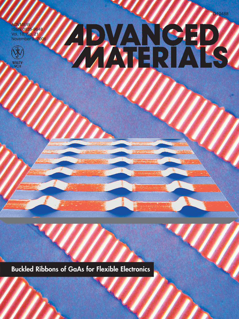
Buckled Ribbons of GaAs for Flexible Electronics

DOI: 10.1002/adma.200600646
Buckled and Wavy Ribbons of GaAs for High-PerformanceElectronics on Elastomeric Substrates**
By Yugang Sun, Vipan Kumar, Ilesanmi Adesida, and John A. Rogers*
Performance capabilities in traditional microelectronics aremeasured mainly in terms of speed, power efficiency, andlevel of integration. Progress in other, more recent, forms ofelectronics is driven instead by the ability to achieve integra-tion on unconventional substrates (e.g., low-cost plastics, foils,paper) or to cover large areas.[1,2] For example, new forms ofX-ray medical diagnosis might be achieved with large-areaimagers that can conformally wrap around the body and digi-tally image the desired tissue.[3] Lightweight, wall-size displaysor sensors that can be deployed onto a variety of surfaces andsurface shapes might provide new technologies for architec-tural design. Various materials including small organic mole-cules,[4–8] polymers,[9] amorphous silicon,[10–12] polycrystallinesilicon,[13–16] single crystalline silicon nanowires,[17,18] and mi-crostructured ribbons[19–22] have been explored to serve assemiconductor channels for the type of thin-film electronicsthat might support these and other applications. These materi-als enable transistors with mobilities that span a wide range(from 10–5 to 500 cm2 V–1 s–1), and in mechanically bendablethin-film formats on flexible substrates. Applications with de-manding high-speed operations, such as large-aperture inter-ferometric synthetic aperture radar (InSAR) and radio fre-quency (RF) surveillance systems, require semiconductorswith much higher mobilities, such as GaAs or InP. The fragil-ity of single crystalline compound semiconductors creates anumber of fabrication challenges that must be overcome in or-der to fabricate high-speed, flexible transistors with them. Werecently established a practical approach to build metal
semiconductor field-effect transistors (MESFETs) on plasticsubstrates by using printed GaAs wire arrays created fromhigh-quality bulk wafers.[23,24] These devices exhibit excellentmechanical flexibility and unity current gain frequencies (fT)that approach 2 GHz, even in moderately scaled devices (e.g.,micrometer gate lengths). The work described in this articledemonstrates GaAs ribbon based MESFETs (as opposed toour previously reported wire devices) designed with specialgeometries that provide not only bendability, but mechanicalstretchability to levels of strain (strain ranges of > 20 %) thatsignificantly exceed the intrinsic yield points of GaAs itself(ca. 2 %). The resulting type of stretchable, high-performanceelectronic systems can provide extremely high levels of bend-ability and the capacity to integrate conformally with curvi-linear surfaces. The work that we report on this GaAs systemextends our recently described “wavy” silicon[25] in four im-portant ways: i) it demonstrates stretchability in GaAs, a ma-terial that is in practical terms much more mechanically frag-ile than Si; ii) it introduces a new “buckled” geometry thatcan be used for stretchability together with or independentlyof the previously described “wavy” configuration; iii) itachieves a new class of stretchable devices (MESFETs); andiv) it demonstrates stretching over a larger range and withgreater symmetry in compression/tension than that previouslyachieved in silicon.
Figure 1 illustrates steps for fabricating stretchable GaAsribbons on an elastomeric substrate made of poly(dimethylsi-loxane) (PDMS). The ribbons were generated from a high-quality bulk wafer of GaAs with multiple epitaxial layers. Thewafer was prepared by growing a 200 nm thick AlAs layer ona (100) semi-insulating GaAs (SI-GaAs) wafer, followed bysequential deposition of a SI-GaAs layer with a thickness of150 nm and Si-doped n-type GaAs layer with a thickness of120 nm and a carrier concentration of 4 × 1017 cm–3. A patternof photoresist lines defined parallel to the (01̄1̄) crystallineorientation served as masks for chemical etching of the epi-layers (including both GaAs and AlAs). Anisotropic etchingwith an aqueous etchant of H3PO4 and H2O2 isolated thesetop layers into individual bars with lengths and orientationsdefined by the photoresist[26,27] and with side walls that formacute angles relative to the wafer surface. Removing thephotoresist after the anisotropic etching and then soaking thewafer in an ethanol solution of HF (2:1 in volume betweenethanol and 49 % aqueous HF) removed the AlAs layer andreleased ribbons of GaAs (n-GaAs/SI-GaAs). The use of eth-anol instead of water for this step reduced cracking that canoccur in the fragile ribbons resulting from the action of capil-
CO
MM
UN
ICATIO
N
Adv. Mater. 2006, 18, 2857–2862 © 2006 WILEY-VCH Verlag GmbH & Co. KGaA, Weinheim 2857
–[*] Prof. J. A. Rogers, Dr. Y. Sun[+]
Department of Materials Science and EngineeringBeckman Institute and Frederick Seitz Materials ResearchLaboratoryUniversity of Illinois at Urbana-ChampaignUrbana, IL 61801 (USA)E-mail: [email protected]. V. Kumar, Prof. I. AdesidaDepartment of Electrical and Computer EngineeringMicro and Nanotechnology LaboratoryUniversity of Illinois at Urbana-ChampaignUrbana, IL 61801 (USA)
[+] Present address: Center for Nanoscale Materials, Argonne NationalLaboratory, Argonne, IL 60439, USA.
[**] This work was supported by the U.S. Department of Energy undergrant DEFG02-91-ER45439. The fabrication and measurements werecarried out using the facilities located in the Microfabrication Labo-ratory and Center for Microanalysis of Materials of Frederick SeitzMaterials Research Laboratory, which are supported by Departmentof Energy. The authors thank Dr. Zheng-Tao Zhu for help in AFMmeasurement and Mr. Matthew A. Meitl for useful discussion.

lary forces during drying. The lower surface tension of ethanolcompared with water also minimized drying induced disorderin the spatial layout of the GaAs ribbons. In the next step, thewafer with released GaAs ribbons was contacted to the sur-face of a prestretched flat slab of PDMS, with the ribbonsaligned with the stretching direction. In this case, van derWaals forces dominate the interaction between PDMS andGaAs. For cases that require stronger interaction strength, wedeposited a thin layer of SiO2 onto the GaAs, and exposedthe PDMS to ultraviolet induced ozone (i.e., product of oxy-gen in air) immediately prior to contact. The ozone creates–Si–OH groups on the surface of PDMS that react with thesurface of the SiO2 upon contact to form bridging siloxane–Si–O–Si– bonds. (The deposited SiO2 is discontinuous at theedges of each ribbon because of the geometry of their side-walls.)[27] For both the weak and strong bonding procedures,peeling the PDMS from the mother wafer transferred all theribbons to the surface of the PDMS. Relaxing the prestrain inthe PDMS led to the spontaneous formation of large-scalebuckles and/or sinusoidal wavy structures along the ribbons.The geometry of the ribbons depends strongly on the pre-strain (defined by DL/L, see Fig. 1) applied to the stamp, theinteraction between the PDMS and the ribbons, and the flex-ural rigidity of the ribbons. For the ribbons investigated here,small prestrains (< 2 %) created highly sinusoidal “waves”with relatively small wavelengths and amplitudes (right, mid-dle frame), for both the strong and weak interaction cases.These geometries in GaAs are similar to those that we re-cently reported for Si.[25] Higher prestrains up to ca. 15 % canbe applied to create similar type of waves where there is a
strong bonding interaction between theribbons and the substrate. A differenttype of geometry, consisting of aperiod-ic “buckles” with relatively large ampli-tudes and widths, formed in the case ofweak interaction strengths and largeprestrains (right, top frame). In addi-tion, our results show that both kinds ofstructures — buckles and waves — cancoexist in a single ribbon whose flexuralrigidity varies along its length (for ex-ample, because of thickness variationsassociated with device structures).
Figure 2 shows several microscopyimages of wavy GaAs ribbons withthicknesses of 270 nm (including bothn-GaAs and SI-GaAs layers) andwidths of 100 lm (all of the ribbons dis-cussed in this paper have widths of100 lm) formed with strong bondingbetween PDMS (thickness of ca. 5 mm)and ribbons. The fabrication followedthe procedures for strong bonding,using 2 nm Ti and 28 nm SiO2 layers on
CO
MM
UN
ICATI
ON
2858 www.advmat.de © 2006 WILEY-VCH Verlag GmbH & Co. KGaA, Weinheim Adv. Mater. 2006, 18, 2857–2862
Figure 1. Schematic illustration of steps for generating “buckled” and “wavy” GaAs ribbons onPDMS substrates. The left bottom frame shows the deposition of thin SiO2 on the surfaces of theribbons to promote strong bonding to the PDMS. This bonding leads to the formation of the wavygeometry shown in the right middle frame. Weak, van der Waals bonding (and moderate to highlevels of prestrain) leads to the buckled geometry, as shown in the right top frame.
Figure 2. Images of wavy GaAs ribbons on a PDMS substrate, as formedwith a prestrain of ca. 1.9 % generated through thermal expansion.A) Optical, B) scanning electron microscopy (SEM), C) 3D atomic forcemicroscopy (AFM), and D) top view AFM images of the same sample.The SEM image was obtained by tilting the sample stage at an angle of45° between sample surface and detection direction. (Spots on the rib-bons might be residues from the sacrificial AlAs layers.) E,F) Surfaceheight profiles plotted along the lines in blue and green as shown in (D),respectively.
the GaAs. A biaxial prestrain of ca. 1.9 % (calculated fromthe thermal response of PDMS)[28] was created in the PDMSby thermal expansion (heating to 90 °C in an oven) immedi-ately prior to and during bonding. This heating also acceler-ated the formation of interfacial siloxane bonds. Cooling thePDMS to room temperature (ca. 27 °C) after transferring theGaAs ribbons released the prestrain. Frames A, B, and C ofFigure 2 show optical microscopy, scanning electron micros-copy (SEM), and atomic force microscopy (AFM) images, re-spectively, of the same sample. The images clearly show theformation of periodic, wavy structures in the GaAs ribbons.The waves were quantitatively analyzed by evaluating linecuts(Fig. 2E and F) from the AFM image in Figure 2D. The con-tour parallel to the longitudinal direction of the ribbon clearlyshows a periodic, wavy profile, consistent with a computed fitto a sine wave (dashed line of Fig. 2E). This result agrees wellwith nonlinear analysis of the initial buckled geometry in auniform, thin, high-modulus layer on a semi-infinite low-mod-ulus support.[25,29] The peak-to-peak amplitude and wave-length associated with this function were determined to be2.56 and 35.0 lm, respectively. The strains computed from theratio of the horizontal distances between the adjacent twopeaks on the stamp (i.e., the wavelength) to their actual con-tour lengths between the peaks (i.e., the surface distancesmeasured by AFM), which we refer to as ribbon strains, yieldvalues (ca. 1.3 %) that are smaller than the prestrain in thePDMS. This difference might be attributed to the low shearmodulus of PDMS and island effects related to the length ofGaAs ribbons being shorter than the length of the PDMS sub-strate.[30] The surface strains of GaAs ribbons at peaks andtroughs, which we refer to as maximum GaAs strains, can beestimated from the ribbon thicknesses and radii of curvatureat the peaks or troughs of the waves according to j h/2, wherej is the curvature. In this evaluation, the direct contributionof strains in the PDMS stamp to the GaAs are ignored be-cause the PDMS can be treated as a semi-infinite supportwhose modulus is low compared to that of GaAs (Young’smodulus of GaAs = 85.5 GPa vs. that of PDMS = 2 MPa). Forthe data of Figure 2E, the maximum GaAs strains areca. 0.62 %, which is more than a factor of two smaller thanthe ribbon strain (i.e., 1.3 %). This mechanical advantage pro-vides stretchability in the GaAs ribbons, with physics similarto that in our recent report on wavy Si.
As shown in Figure 2F, the peak and trough regions of the rib-bons are higher and lower than the contour level (right portionof the green curve) of the surface of pristine PDMS (i.e., theareas without ribbons), respectively. The result suggests that thePDMS under the GaAs adopts a wavy profile as a result of theupward and downward forces imparted to the PDMS by theGaAs ribbons in the peaks and troughs, respectively. The precisegeometry of the PDMS near the peaks of the waves is very diffi-cult to evaluate directly. We suspect that in addition to the up-ward deformation there is also a lateral necking caused by thePoisson effect. The wavy ribbons on the PDMS stamp can bestretched and compressed by applying strains to the PDMS (so-called applied strain denoted as positive for stretching and nega-
tive for compressing). The insets of Figure 2A and B show im-ages of the ribbons stretched (ca. 1.5 %) to a flat geometry.Further stretching transfers more tensile strain to the flat GaAsribbons, resulting in their breakage when this excess strainreaches the failure strain of GaAs. Compressive strains appliedto the substrate reduce the wavelengths and increase the ampli-tudes of the wavy ribbons. Failure in compression occurs whenthe bending strains at peaks (and troughs) exceed the failurestrains. This variation of wavelength with strain is consistent withprevious observations in silicon, and is different from the predic-tions of wavelength invariance derived from ideal models.[29]
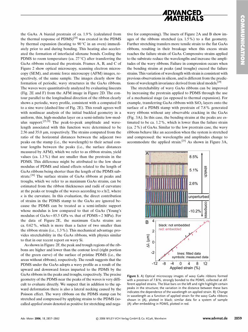
The stretchability of wavy GaAs ribbons can be improvedby increasing the prestrain applied to PDMS through the useof a mechanical stage (as opposed to thermal expansion). Forexample, transferring GaAs ribbons with SiO2 layers onto thesurface of a PDMS stamp with prestrain of 7.8 % generatedwavy ribbons without any observable cracking in the GaAs(Fig. 3A). In this case, the bending strains at the peaks are es-timated to be ca. 1.2 %, which is lower than the failure strain(ca. 2 %) of GaAs. Similar to the low prestrain case, the wavyribbons behave like an accordion when the system is stretchedand compressed: the wavelengths and amplitudes change toaccommodate the applied strain.[25] As shown in Figure 3A,
CO
MM
UN
ICATIO
N
Adv. Mater. 2006, 18, 2857–2862 © 2006 WILEY-VCH Verlag GmbH & Co. KGaA, Weinheim www.advmat.de 2859
Figure 3. A) Optical microscopy images of wavy GaAs ribbons formedwith a prestrain of 7.8 %, strongly bonded to the PDMS, collected at dif-ferent applied strains. The blue bars on the left and right highlight certainpeaks in the structure; the variation in the distance between these barsindicates the dependence of the wavelength on applied strain. B) Changein wavelength as a function of applied strain for the wavy GaAs ribbonsshown in (A), plotted in black; similar data for a system of sample(A) after embedding in PDMS, plotted in red.

the wavelengths increase with tensile strain until the ribbonsbecome flat and decrease with compressive strain until theribbons break. These deformations are completely reversible,and do not involve any measurable slipping of the GaAs onthe PDMS. The wavelength changes linearly with appliedstrains in both compression and tension (see, the black linesand symbols in Fig. 3B), in contrast to the mildly asymmetricbehavior observed in Si ribbons with weak bonding and muchlower prestrains.[25] The variation of wavelength with appliedstrains is in agreement with full finite element modeling of themechanics of the system.
In practical applications, it might be useful to encapsulate theGaAs ribbons and devices in a way that maintains their stretch-ability. As a simple demonstration of one possibility, we castand cured PDMS prepolymers on samples such as the oneshown in Figure 3A to embed the ribbons in PDMS. The em-bedded systems exhibit similar mechanical behavior to the un-embedded ones, i.e., stretching the system increases wavelengthand compressing the system decreases wavelength (the red linesand symbols in Fig. 3B). Shrinkage resulting from curing of thesecond layer of PDMS generated some moderate amount of ad-ditional strain (ca. 1 %). This strain resulted in a slight decreasein the wavelength of the wavy ribbons, thereby expandingslightly the range of stretchability. Figure 3B shows the differ-ence. Overall, the systems generated with prestrain of ca. 7.8 %can be stretched or compressed to strains of up to ca. 10 %without inducing any observable breakage in the GaAs.
The wavy GaAs ribbons on PDMS substrates can be usedto fabricate high-performance electronic devices, such asMESFETs, the electrodes of which areformed through metallization and pro-cessing on the wafer, before transfer toPDMS. These metal layers change theflexural rigidity of the ribbons in aspatially dependent manner. Figure 4Ashows GaAs ribbons integrated withohmic stripes (source and drain elec-trodes) and Schottky contacts (gate elec-trodes) after transfer to a PDMS sub-strate with prestrain of ca. 1.9 %. Theohmic contacts consisted of metal stacksincluding AuGe (70 nm)/Ni (10 nm)/Au(70 nm) formed on the original wafersthrough lithographically defined masksalong with sequential annealing of thewafers at elevated temperature (450 °Cfor 1 min) in a quartz tube with flowingN2. These ohmic segments had lengthsof 500 lm. The distances between twoadjacent ohmic contacts were 500 lm(i.e., channel length). Schottky contactswith lengths of 240 lm (i.e., gate length)were generated by directly depositinga 75 nm Cr layer and a 75 nm Aulayer through electron-beam evapora-tion against the photolithographically
defined mask. The electrodes had widths equal to the GaAsribbons, i.e., 100 lm; their relatively large sizes facilitate prob-ing. (The dimensions of electrodes and semiconductor chan-nels can be significantly decreased to achieve enhanced deviceperformance.)[24] As shown in Figure 4A, these stretchableGaAs MESFETS exhibit, short-range, periodic waves only inthe regions without electrodes. The absence of waves in thethicker regions might be attributed to their enhanced flexuralrigidity mainly because of the additional thickness associatedwith the metals. Periodic waves could be initiated in the thickerregions by using prestrains larger than ca. 3 %. In these cases,however, the ribbons tend to break at the edges of the metalelectrodes because of critical flaws and/or high peak strainsnear these edges. This failure mode limits the stretchability.
To circumvent this limitation, we reduced the strength of in-teraction between the MESFETs and the PDMS by eliminat-ing the siloxane bonding. For such samples, prestrain > 3 %generated large, aperiodic buckles with relatively large widthsand amplitudes because of physical detachment of the ribbonsfrom the PDMS surface. Figure 4B presents this type of sys-tem, as prepared with a prestrain of ca. 7 %, in which the bigbuckles form in the thinner regions of the devices. The detach-ment seems to extend slightly to the thicker sections withohmic stripes, as indicated by the vertical lines. The contrastvariation along ribbons is attributed to reflections and refrac-tion-associated passage of light through the curved GaAs seg-ments. The SEM image (Fig. 4C) clearly shows the formationof arc-shaped buckles and flat, unperturbed PDMS. Thesebuckles display asymmetric profiles (as indicated by the red
CO
MM
UN
ICATI
ON
2860 www.advmat.de © 2006 WILEY-VCH Verlag GmbH & Co. KGaA, Weinheim Adv. Mater. 2006, 18, 2857–2862
Figure 4. Images of GaAs ribbons integrated with ohmic (source and drain) and Schottky (gate)contacts to form complete MESFETs. A) Optical microscopy images of wavy ribbons formed usinga prestrain of 1.9 % and strong bonding to the PDMS, showing the formation of periodic wavesonly in the sections without electrodes (grey). B) Optical and C) SEM images of buckled ribbonsformed with a prestrain of ca. 7 % and weak bonding to the PDMS. D) Optical image of twobuckled devices shown in (B) after they were stretched to be flat. E) A set of optical images of anindividual ribbon device shown in (B) with different external applied strains (from top to bottom:compressing strain of 5.83 %, no applied strain, and stretching strain of 5.83 %) after it was em-bedded in PDMS.

curves) with tails with ohmic contacts to the sides. This asym-metry might be attributed to the unequal lengths (500 lmversus 240 lm) of ohmic stripes and Schottky contacts forindividual transistors. This kind of buckled MESFET can bestretched to its original flat status (Fig. 4D) with appliedstretching strains between ca. 6 % and ca. 7 %. However,compressing the system shown in Figure 4B leads to continu-ous detachment of ribbons from the PDMS surface to formlarger buckles because of weak bonding. Embedding such de-vices in PDMS according to the previously described proce-dures eliminates this type of uncontrolled behavior. Figure 4Bshows such a system, in which the liquid PDMS precursor fillsthe gaps underneath the buckles. The fully surrounding PDMSconfines the ribbons and prevents them from sliding and de-taching. The embedded devices can be reversibly stretchedand compressed to strains up to ca. 6 % without breaking theribbons. It is notable that when the embedded system wascompressed by –5.83 % (top frame of Fig. 4E), periodic, smallwaves formed in the regions with metal electrodes as well asnew ripples in the buckled regions. The formation of thesenew small waves in combination with the large buckles en-hances the compressibility. Stretching the system forces thebuckled regions to compress and stretch the PDMS in a man-ner that enables some flattening of these buckles, therebyelongating the projected lengths of the ribbons (bottom frameof Fig. 4E). These results suggest that embedded devices withbig buckles, which are a kind of geometry distinct from thewaves, represent a promising method to achieve stretchabilityand compressibility that can be used in combination with orseparately from the wavy approach.
The performance of buckled devices can be evaluated bydirectly probing the current flow from source to drain. Fig-ure 5A shows GaAs-ribbon devices fabricated on a wafer,picked up using a flat PDMS stamp and transfer printed onto aPDMS substrate with a prestrain of 4.7 %. In this configuration,the metal electrodes are exposed to air for electrical probing.After the prestretched PDMS was relaxed to a strain of 3.4 %,periodic small waves formed in the thin regions of the MESFET(the second frame of Fig. 5A). When the prestretched PDMSstamp was fully relaxed, the small waves in each segment of pureGaAs coalesced into an individual big buckle (the third frame ofFig. 5A). The buckled devices could be stretched to their flatstatus with an applied stretching strain of 4.7 % (see the bottomframe of Figure 5A). The current–voltage (I–V) curves of thesame device with applied strains of 0.0 % (the third frame ofFig. 5A) and 4.7 % (the bottom frame of Fig. 5A) are plotted inFigure 5B with red and black colors, respectively. The results in-dicate that the current flow from source to drain of buckledMESFETs on PDMS substrates can be well modulated with thevoltages applied to the gate and that the applied stretching straingenerates only a minor effect on device performance.
In summary, an approach has been developed to form“buckled” and “wavy” GaAs ribbons onto or embedded inPDMS elastomeric substrates. The geometrical configurationsof these ribbons depend on the levels of prestrains used in thefabrication, the strength of interactions between the PDMS
and ribbons, and on the thicknesses and types of materialsused. Buckled and wavy ribbons of GaAs multilayer stacks andfully formed MESFET devices show large levels of compress-ibility/stretchability, because of the ability of their geometriesto adjust in a manner that can accommodate applied strainswithout transferring those strains to the materials themselves.Successful realization of large levels of mechanical stretchabil-ity (and, as a result, other attractive mechanical characteristicssuch as extreme bendability) in an intrinsically fragile materiallike GaAs suggests that similar strategies might be applicableto a wide range of other materials classes. These possibilities,alternative geometrical strategies to achieve similar mechani-cal characteristics, and detailed mechanical modeling of thesesystems represent topics of current work.
Experimental
GaAs wafers with custom-designed epitaxial layers (details de-scribed in the text) were purchased from IQE Inc., Bethlehem, PA.The lithographic processes employed AZ photoresist, i.e., AZ 5214and AZ nLOF 2020 for positive and negative imaging, respectively.The GaAs wafers with photoresist mask patterns were anisotropicallyetched in the etchant (4 mL H3PO4 (85 wt %), 52 mL H2O2
(30 wt %), and 48 mL deionized water) that was cooled in the ice–water bath. The AlAs layers were dissolved with a diluted HF solution(Fisher Chemicals) in ethanol (1:2 in volume). The samples with re-
CO
MM
UN
ICATIO
N
Adv. Mater. 2006, 18, 2857–2862 © 2006 WILEY-VCH Verlag GmbH & Co. KGaA, Weinheim www.advmat.de 2861
Figure 5. A) Optical images of a GaAs ribbon MESFET on a PDMS stampwith different strains built into the PDMS substrate. The prestrain ap-plied to the PDMS stamp was 4.7 % before the devices were transferredonto its surface. B) Comparison of drain source current–voltage (I–V)curves for the device shown in (A) before and after 4.7 % stretchingstrain was applied to the system; IDS: drain-source current, VDS: drain-source voltage.

leased ribbons on mother wafers were dried in a fume hood. The driedsamples were placed in the chamber of an electron-beam evaporator(Temescal FC-1800) and were coated with sequential layers of 2 nmTi and 28 nm SiO2. The metals for the MESFET devices were depos-ited by electron-beam evaporation before removal of the AlAs layers.A PDMS stamp with thickness of ca. 5 mm was prepared by pouringthe mixture of low-modulus PDMS (component ratio A:B = 1:10,Sylgard 184, Dow Corning) onto a piece of silicon wafer premodifiedwith monolayer of (tridecafluoro-1,1,2,2-tetrahydrooctyl)-1-trichloro-silane, followed by baking at 65 °C for 4 h. In order to generate strongbonding, the stamps were exposed to UV light in air for 5 min. In thetransfer process, the stamps were stretched through thermal expan-sion (in oven) and/or mechanical forces. The wafers with released rib-bons were then laminated on the surfaces of the stretched PDMSstamps and left in contact at elevated temperatures (dependent on therequired prestrains) for 5 min. The mother wafers were peeled fromthe stamps and all the ribbons were transferred to stamps. The pre-strains applied to the stamps were released through cooling down toroom temperature and/or removing the mechanical forces, resulting inthe formation of wavy profiles along ribbons. In the mechanical evalu-ations, we used a specially designed stage to stretch as well as com-press the PDMS stamps with “wavy” and “buckled” GaAs ribbons.
Received: March 26, 2006Published online: October 10, 2006
–[1] R. H. Reuss, B. R. Chalamala, A. Moussessian, M. G. Kane,
A. Kumar, D. C. Zhang, J. A. Rogers, M. Hatalis, D. Temple,G. Moddel, B. J. Eliasson, M. J. Estes, J. Kunze, E. S. Handy, E. S.Harmon, D. B. Salzman, J. M. Woodall, M. A. Alam, J. Y. Murthy,S. C. Jacobsen, M. Olivier, D. Markus, P. M. Campbell, E. Snow,Proc. IEEE 2005, 93, 1239.
[2] K. Jain, M. Klosner, M. Zemel, S. Raghunandan, Proc. IEEE 2005,93, 1500.
[3] A. Nathan, B.-K. Park, Q. Ma, A. Sazonov, J. A. Rowlands, Micro-electron. Reliab. 2002, 42, 735.
[4] a) H. Sirringhaus, Adv. Mater. 2005, 17, 2411. b) S. R. Forrest,Nature 2004, 428, 911. c) C. R. Newman, C. D. Frisbie, D. A.da Silva, J.-L. Brédas, P. C. Ewbank, K. R. Mann, Chem. Mater.2004, 16, 4436. d) H. E. Katz, Z. Bao, S. Gilat, Acc. Chem. Res. 2001,34, 359. e) H. E. Katz, Chem. Mater. 2004, 16, 4748. f) Y. Sun, Y. Liu,D. Zhu, J. Mater. Chem. 2005, 15, 53.
[5] a) D. Knipp, R. A. Street, A. Völkel, J. Ho, J. Appl. Phys. 2003, 93,347. b) C.-W. Chu, S.-H. Li, C.-W. Chen, V. Shrotriya, Y. Yang, Appl.Phys. Lett. 2005, 87, 193 508. c) B. S. Ong, Y. Wu, P. Liu, Proc. IEEE2005, 93, 1412.
[6] a) G. H. Gelinck, H. E. A. Juitema, E. Van Veenendaal, E. Canta-tore, L. Schrijnemakers, J. B. P. H. Van der Putten, T. C. T. Geuns,M. Beenhakkers, J. B. Giesbers, B.-H. Huisman, E. J. Meijer, E. M.Benito, F. J. Touwslager, A. W. Marsman, B. J. E. Van Rens, D. M.de Leeuw, Nat. Mater. 2004, 3, 106. b) J. A. Rogers, Z. Bao, K. Bald-win, A. Dodabalapur, B. Crone, V. R. Raju, V. Kuck, H. Katz,K. Amundson, J. Ewing, P. Drzaic, Proc. Natl. Acad. Sci. USA 2001,98, 4935. c) T. Someya, Y. Kato, S. Iba, Y. Noguchi, T. Sekitani,H. Kawaguchi, T. Sakurai, IEEE Trans. Electron Devices 2005, 52,2502. d) T. Someya, Y. Kato, T. Sekitani, S. Iba, Y. Noguchi, Y. Murase,H. Kawaguchi, T. Sakurai, Proc. Natl. Acad. Sci. USA 2005, 102, 12 321.
[7] a) V. C. Sundar, J. Zaumseil, V. Podzorov, E. Menard, R. L. Willett,T. Someya, M. E. Gershenson, J. A. Rogers, Science 2004, 303, 1644.b) E. Menard, V. Podzorov, S.-H. Hur, A. Gaur, M. E. Gershenson,J. A. Rogers, Adv. Mater. 2004, 16, 2097. c) V. Podzorov, E. Menard,J. A. Rogers, M. E. Gershenson, Phys. Rev. Lett. 2005, 95, 226 601.d) W.-Y. Chou, H.-L. Cheng, Adv. Funct. Mater. 2004, 14, 811.e) M. Mas-Torrent, P. Hadley, N. Crivillers, J. Veciana, C. Rovira,ChemPhysChem 2006, 7, 86.
[8] a) M. Halik, H. Klauk, U. Zschieschang, G. Schmid, C. Dehm,M. Schütz, S. Maisch, F. Effenberger, M. Brunnbauer, F. Stellacci,
Nature 2004, 431, 963. b) M.-H. Yoon, H. Yan, A. Facchetti, T. J.Marks, J. Am. Chem. Soc. 2005, 127, 10 388. c) Y. Jang, D. H. Kim,Y. D. Park, J. H. Cho, M. Hwang, K. Cho, Appl. Phys. Lett. 2006, 88,072 101.
[9] a) M. C. Hamilton, S. Martin, J. Kanicki, Chem. Mater. 2004, 16,4699. b) M. J. Deen, M. H. Kazemeini, Y. M. Haddara, J. Yu,G. Vamvounis, S. Holdcroft, W. Woods, IEEE Trans. Electron De-vices 2004, 51, 1892. c) K. Cheng, M.-H. Yang, W. W. W. Chiu, C.-Y.Huang, J. Chang, T.-F. Ying, Y. Yang, Macromol. Rapid Commun.2005, 26, 247.
[10] a) E. Fortunato, L. Pereira, H. Águas, I. Ferreira, R. Martins, Proc.IEEE 2005, 93, 1281. b) A. Sazonov, D. Striakhilev, C.-H. Lee,A. Nathan, Proc. IEEE 2005, 93, 1420. c) A. J. Flewitt, W. I. Milne,Proc. IEEE 2005, 93, 1364. d) P. Servati, A. Nathan, Proc. IEEE2005, 93, 1257.
[11] a) C.-S. Yang, L. L. Smith, C. B. Arthur, G. N. Parsons, J. Vac. Sci.Technol. B 2000, 18, 683. b) P. I. Hsu, H. Gleskova, M. Huang,Z. Suo, S. Wagner, J. C. Sturm, J. Non-Cryst. Solids 2002, 299–302,1355.
[12] Y. Chen, J. Au, P. Kazlas, A. Ritenour, H. Gates, M. McCreary,Nature 2003, 423, 136.
[13] a) M. Wu, S. Wagner, Appl. Phys. Lett. 2001, 78, 3729. b) S. Wagner,H. Gleskova, I.-C. Cheng, M. Wu, Thin Solid Films 2003, 430, 15.c) M. Wu, S. Wagner, Appl. Surf. Sci. 2001, 175–176, 753.
[14] a) S. V. Karnik, M. K. Hatalis, Jpn. J. Appl. Phys., Part 1 2003, 42,1200. b) S. V. Karnik, M. K. Hatalis, Solid-State Electron. 2003, 47,653.
[15] P. K. Shetty, N. D. Theodore, J. Ren, J. Menendez, H. C. Kim,E. Misra, J. W. Mayer, T. L. Alford, Mater. Lett. 2005, 59, 872.
[16] A. Imparato, C. Minarini, A. Rubino, P. Tassini, F. Villani, D. D.Sala, E. Amendola, M. Kunst, H.-C. Neitzert, S. Bellone, Thin SolidFilms 2005, 487, 58.
[17] X. Duan, C. Niu, V. Sahi, J. Chen, J. W. Parce, S. Empedocles, J. L.Goldman, Nature 2003, 425, 274.
[18] M. C. McAlpine, R. S. Friedman, S. Jin, K.-H. Liu, W. U. Wang,C. M. Lieber, Nano Lett. 2003, 3, 1531.
[19] E. Menard, K. J. Lee, D.-Y. Khang, R. G. Nuzzo, J. A. Rogers, Appl.Phys. Lett. 2004, 84, 5398.
[20] E. Menard, R. G. Nuzzo, J. A. Rogers, Appl. Phys. Lett. 2005, 86,093 507.
[21] Z.-T. Zhu, E. Menard, K. Hurley, R. G. Nuzzo, J. A. Rogers, Appl.Phys. Lett. 2005, 86, 133 507.
[22] K. J. Lee, M. J. Motala, M. A. Meitl, W. R. Childs, E. Menard, A. K.Shim, J. A. Rogers, R. G. Nuzzo, Adv. Mater. 2005, 17, 2332.
[23] Y. Sun, S. Kim, I. Adesida, J. A. Rogers, Appl. Phys. Lett. 2005, 87,083 501.
[24] Y. Sun, E. Menard, J. A. Rogers, H.-S. Kim, S. Kim, G. Chen, I. Ade-sida, R. Dettmer, R. Cortez, A. Tewksbury, Appl. Phys. Lett. 2006,88, 183 509.
[25] D.-Y. Khang, H. Jiang, Y. Huang, J. A. Rogers, Science 2006, 311,208.
[26] Y. Sun, J. A. Rogers, Nano Lett. 2004, 4, 1953.[27] Y. Sun, D.-Y. Khang, F. Hua, K. Hurley, R. G. Nuzzo, J. A. Rogers,
Adv. Funct. Mater. 2005, 15, 30.[28] The thermally induced prestrain is ascribed to thermal expansion of
the PDMS stamp, which has a bulk linear coefficient of thermalexpansion of aL= 3.1 × 10⁻⁴ lm lm–1 °C–1. T. Buma, M. Spisar,M. O’Donnell, Appl. Phys. Lett. 2001, 79, 548. On the other hand,the coefficient of thermal expansion for GaAs is only5.73 × 10–6 lm lm–1 °C–1. Therefore, the prestrain on PDMS (rela-tively GaAs ribbons) for the sample that was prepared at 90 °C andcooled down to 27 °C was determined according toDaL · DT = (3.1 × 10⁻⁴ – 5.73 × 10–6) × (90 – 27) = 1.9 %.
[29] Z. Y. Huang, W. Hong, Z. Suo, J. Mech. Phys. Solids 2005, 53, 2101.[30] S. Wagner, S. P. Lacour, J. Jone, P.-H. I. Hsu, J. C. Sturm, T. Li,
Z. Suo, Phys. E 2005, 25, 326.
CO
MM
UN
ICATI
ON
2862 www.advmat.de © 2006 WILEY-VCH Verlag GmbH & Co. KGaA, Weinheim Adv. Mater. 2006, 18, 2857–2862