final report on ldrd project: single-photon … · final report on ldrd project: ... higher dark...
TRANSCRIPT

3
SAND2006-7420 Unlimited Release
Printed November 2006
Final Report on LDRD Project: Single-Photon-Sensitive Imaging Detector Arrays at 1600 nm
Malcolm S. Carroll, Darwin K. Serkland, Kent Childs, Robert Koudelka, Kent M. Geib, Tom Bauer, John Klem, Josephine Sheng, Desta Bolles, Sam Hawkins, and Rupal Patel
Photonic Microsystems Technology Department
Sandia National Laboratories P. O. Box 5800
Albuquerque, New Mexico 87185-0603
Abstract The key need that this project has addressed is a short-wave infrared light detector for ranging (LIDAR) imaging at temperatures greater than 100K, as desired by non-proliferation and work for other customers. Several novel device structures to improve avalanche photodiodes (APDs) were fabricated to achieve the desired APD performance. A primary challenge to achieving high sensitivity APDs at 1550 nm is that the small band-gap materials (e.g., InGaAs or Ge) necessary to detect low-energy photons exhibit higher dark counts and higher multiplication noise compared to materials like silicon. To overcome these historical problems APDs were designed and fabricated using separate absorption and multiplication (SAM) regions. The absorption regions used (InGaAs or Ge) to leverage these materials 1550 nm sensitivity. Geiger mode detection was chosen to circumvent gain noise issues in the III-V and Ge multiplication regions, while a novel Ge/Si device was built to examine the utility of transferring photoelectrons in a silicon multiplication region. Silicon is known to have very good analog and GM multiplication properties. The proposed devices represented a high-risk for high-reward approach. Therefore one primary goal of this work was to experimentally resolve uncertainty about the novel APD structures. This work specifically examined three different designs. An InGaAs/InAlAs Geiger mode (GM) structure was proposed for the superior multiplication properties of the InAlAs. The hypothesis to be tested in this structure was whether InAlAs really presented an advantage in GM. A Ge/Si SAM was proposed representing the best possible multiplication material (i.e., silicon), however, significant uncertainty existed about both the Ge material quality and the ability to transfer photoelectrons across the Ge/Si interface. Finally a third pure germanium GM structure was proposed because bulk germanium has been reported to have better dark count properties. However, significant uncertainty existed about the quantum efficiency at 1550 nm the necessary operating temperature. This project has resulted in several conclusions after fabrication and measurement of the proposed structures. We have successfully demonstrated the Ge/Si proof-of-concept in producing high analog gain in a silicon region while absorbing in a Ge region. This has included significant Ge processing infrastructure development at Sandia. However, sensitivity is limited at low temperatures due to high dark currents that we ascribe to

4
tunneling. This leaves remaining uncertainty about whether this structure can achieve the desired performance with further development. GM detection in InGaAs/InAlAs, Ge/Si, Si and pure Ge devices fabricated at Sandia was shown to overcome gain noise challenges, which represents critical learning that will enable Sandia to respond to future single photon detection needs. However, challenges to the operation of these devices in GM remain. The InAlAs multiplication region was not found to be significantly superior to current InP regions for GM, however, improved multiplication region design of InGaAs/InP APDs has been highlighted. For Ge GM detectors it still remains unclear whether an optimal trade-off of parameters can achieve the necessary sensitivity at 1550 nm. To further examine these remaining questions, as well as other application spaces for these technologies, funding for an Intelligence Community post-doc was awarded this year.
5
Acknowledgments
We gratefully acknowledge the expert technical assistance that was provided by Gary D. Karpen, Tom Headley, Rob Jarecki, Bob Cordova, S. Habermehl. Sandia is a multiprogram laboratory operated by Sandia Corporation, a Lockheed Martin Company, for the United States Department of Energy’s National Nuclear Security Administration under contract DE-AC04-94AL85000.
6
Contents
1. Introduction ................................................................................ 9
1.1. LDRD Project Overview .............................................................................9
1.2. Technical Problem and Approach ..............................................................9
2. Design and Fabrication of Ge/Si Avalanche Photodiodes ... 12
2.1. APD Design..............................................................................................12
2.2. Germanium deposition development........................................................13 2.2.1 Experimental Details ...................................................................................................................... 13 2.2.2 Discussion....................................................................................................................................... 13 2.2.3 References ...................................................................................................................................... 18
2.3. Germanium on Silicon Epitaxy Development ...........................................19 2.3.1 Background..................................................................................................................................... 19 2.3.2 Experiment & Discussion ............................................................................................................... 20 2.3.3 Summary of results ......................................................................................................................... 23 2.3.4 References ...................................................................................................................................... 23
2.4. Germanium-Silicon Device Fabrication ....................................................25 2.4.1 Overview of process flow............................................................................................................... 25
2.5. Ge-Si Device Performance.......................................................................26 2.5.1 Description of final device............................................................................................................. 26 2.5.2 Room temperature I-V.................................................................................................................... 27 2.5.3 Responsivity ................................................................................................................................... 30 2.5.4 Performance at reduced temperature .............................................................................................. 31 2.5.5 Geiger mode operation of Ge-Si APD ............................................................................................ 32 2.5.6 Summary of Ge-Si APD performance ............................................................................................ 35 2.5.7 References ...................................................................................................................................... 36
3. Pure Germanium Geiger Mode APDs ..................................... 37
3.1. Design of Ge Geiger Mode APDs ............................................................37 3.1.2. Approach ....................................................................................................................................... 38 3.1.3. References ..................................................................................................................................... 38
3.2. Fabrication of Ion Implanted Ge APDs.....................................................39 3.2.1 Device fabrication (diffusion after Implantation) .......................................................................... 39 3.2.1 Experiment & discussion ................................................................................................................ 39 3.2.2 Summary of phosphorus diffusion in germanium........................................................................... 43 3.2.3 References ..................................................................................................................................... 44
3.3. Germanium APD Device Fabrication .......................................................44
3.4. Ge APD Device Performance...................................................................46
4. InGaAs Based Avalanche Photodiodes ................................. 47
4.1. InGaAs/InAlAs APDs................................................................................47 4.1.1 InGaAs/InAlAs APD Device Design and Fabrication .............................................................. 47 4.1.2 InGaAs/InAlAs APD Device Characterization ......................................................................... 49

7
4.1.3 Conclusion of InGaAs APD research........................................................................................ 54 4.1.4 References ................................................................................................................................. 55
5. Impact of Technical Risk ......................................................... 55
6. Publications and Presentations Resulting from this LDRD . 56
7. Awards/Leadership Related to this LDRD ............................. 57
7.1. Awards .....................................................................................................57
7.2. Intellectual Property .................................................................................57
7.3. People......................................................................................................57
7.4. Collaborations ..........................................................................................58
7.5. Further work .............................................................................................58
7.6. Other significant impacts ..........................................................................58
8. Conclusions.............................................................................. 58

8
(This page is left blank intentionally.)

9
1. Introduction
1.1. LDRD Project Overview
We proposed to develop avalanche photodiodes (APDs) to attempt to achieve low dark counts (< 4.5x10¹² events-sec-1-cm-2), high multiplication (> 300), and high quantum efficiency at 1600 nm (> 10%) for single-photon-sensitive imaging detector arrays. These targets would constitutes a new optoelectronic device capability that can scale to fairly large imaging arrays (256 x 256), given sufficient program area investment, and the key need this work addressed was a short-wave infrared light detection and ranging (LIDAR) imaging at temperatures greater than 220K, as desired by non-proliferation and work for other (WFO) customers.
A primary challenge to achieving high sensitivity APDs at 1600 nm is that the small band-gap materials (e.g., InGaAs or Ge) necessary to detect low-energy photons exhibit higher dark counts (due to high tunneling or diffusion currents) and higher multiplication noise (due to non-ideal ratios of electron and hole ionization coefficients) compared to materials with larger band-gaps (e.g., Si).
To overcome these historical performance problems we designed and fabricated APDs using separate absorption and multiplication (SAM) regions to leverage the 1600 nm sensitivity of either InGaAs or Ge, while achieving silicon-like multiplication properties in either Si, SiGe or heterostructure engineered InGaAlAs multiplication regions. The novel integration of small and large bandgap materials promises to be a significant scientific challenge that will expand the capabilities of Sandia’s MESA program.
1.2. Technical Problem and Approach
No single semiconductor material has the necessary combination of properties (e.g., bandgap, intrinsic carrier concentration, and ionization coefficients) to produce an avalanche photodiode (APD) that has a quantum efficiency > 10% at 1600 nm, low noise and high enough gain to satisfy certain nonproliferation imaging applications. An established approach in APD design to circumvent the limitations of a single material is to use separate absorption and multiplication (SAM) regions. However, the combination of non-ideal carrier ionization properties in III-V materials and challenges to lattice matching Si with a narrow bandgap material has prevented the demonstration of an ideal SAM-APD with both 1600 nm sensitivity and multiplication performance similar to silicon APDs. In order to overcome this challenge, we must either engineer a III-V material to have improved multiplication properties or develop a novel technique to integrate a narrow bandgap material with silicon.
Three approaches are outlined below that could improve the APD performance through either engineering of the multiplication region or through novel approaches to materials integration in the APD. Design and fabrication techniques to avoid cross-talk issues between pixels in the array will likely rely on deep trench or mesa isolation in the future, which has already shown promise in small arrays [2]. Narrow Bandgap Material Integration with Si
10
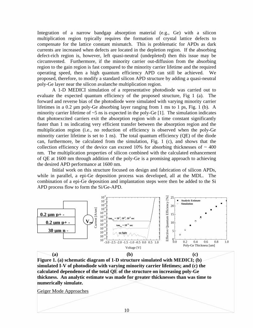
Integration of a narrow bandgap absorption material (e.g., Ge) with a silicon multiplication region typically requires the formation of crystal lattice defects to compensate for the lattice constant mismatch. This is problematic for APDs as dark currents are increased when defects are located in the depletion region. If the absorbing defect-rich region is, however, left quasi-neutral (undepleted) then this issue may be circumvented. Furthermore, if the minority carrier out-diffusion from the absorbing region to the gain region is fast compared to the minority carrier lifetime and the required operating speed, then a high quantum efficiency APD can still be achieved. We proposed, therefore, to modify a standard silicon APD structure by adding a quasi-neutral poly-Ge layer near the silicon avalanche multiplication region.
A 1-D MEDICI simulation of a representative photodiode was carried out to evaluate the expected quantum efficiency of the proposed structure, Fig 1 (a). The forward and reverse bias of the photodiode were simulated with varying minority carrier lifetimes in a 0.2 µm poly-Ge absorbing layer ranging from 1 ms to 1 ps, Fig. 1 (b). A minority carrier lifetime of ~5 ns is expected in the poly-Ge [1]. The simulation indicates that photoexcited carriers exit the absorption region with a time constant significantly faster than 1 ns indicating very efficient transfer between the absorption region and the multiplication region (i.e., no reduction of efficiency is observed when the poly-Ge minority carrier lifetime is set to 1 ns). The total quantum efficiency (QE) of the diode can, furthermore, be calculated from the simulation, Fig. 1 (c), and shows that the collection efficiency of the device can exceed 10% for absorbing thicknesses of ~ 400 nm. The multiplication properties of silicon combined with the calculated enhancement of QE at 1600 nm through addition of the poly-Ge is a promising approach to achieving the desired APD performance at 1600 nm.
Initial work on this structure focused on design and fabrication of silicon APDs, while in parallel, a epi-Ge deposition process was developed, all at the MDL. The combination of a epi-Ge deposition and implantation steps were then be added to the Si APD process flow to form the Si/Ge-APD.
(a) (b) (c) Figure 1. (a) schematic diagram of 1-D structure simulated with MEDICI; (b) simulated I-V of photodiode with varying minority carrier lifetimes; and (c) the calculated dependence of the total QE of the structure on increasing poly-Ge thickness. An analytic estimate was made for greater thicknesses than was time to numerically simulate.
Geiger Mode Approaches
0.0 0.2 0.4 0.6 0.8 1.00
5
10
15
20
25 Analytic Estimate Simulation
Effe
ctiv
e Q
uant
um E
ffic
ienc
y [%
]
Poly-Ge Thickness [um]
Vap
0.2 µm p+ - 0.2 µm p+ - 30 µm n -
-3.0 -2.5 -2.0 -1.5 -1.0 -0.5 0.0 0.5 1.010-1710-1610-1510-1410-1310-1210-1110-1010-910-810-710-6
no light
tauGe = 10-12 sec
Cur
rent
[A/u
m]
Voltage [V]
tauGe
= 10-3, 10-6, 10-9 sec

11
Recent work on single photon detection has shown that the gain noise problem may be completely circumvented through operating the avalanche photodiode in Geiger mode. This mode of operation automatically provides the necessary gain and can show very high timing precision (i.e. sub-nanosecond) for single photon arrivals. Geiger mode InGaAs/InP APDs have already been demonstrated elsewhere and show sufficient quantum efficiency for the desired imaging applications (~10%) (e.g., 213K). However, a critical challenge to 1550 nm Geiger mode operation is reducing the dark count rate to a level that is practical for NP&A imaging purposes, while still sustaining a high detection efficiency. Device design and simulation of these devices has focused on developing structures to minimize noise producing mechanisms (e.g., tunneling, SRH generation and charge traps), while maximizing detection efficiency and operating temperature. Dark count rates are believed to be smaller in APDs with larger ratio of electron and hole impact ionization coefficients (k = αe / αh), therefore, an InGaAs APD was designed with an InAlAs multiplication region because InAlAs is known to have a larger k than InP.
A germanium Geiger mode APD design has also been pursued because dark count rates are also known to depend on charge trap states and the electron minority carrier lifetime in the APD structure. Extremely long minority carrier lifetimes (> 10-3 sec) and low charge trap densities can be achieved in germanium APDs, which suggests that dark count rates may be improved over state of the art InGaAs Geiger mode devices. The substrate doping was, furthermore, selected to minimize tunneling (low doping for lower electric fields) and depletion width (high doping for reduced diffusion and thermal generation).
12
2. Design and Fabrication of Ge/Si Avalanche Photodiodes
2.1. APD Design
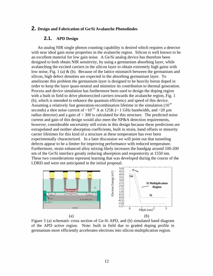
An analog NIR single photon counting capability is desired which requires a detector with near ideal gain noise properties in the avalanche region. Silicon is well known to be an excellent material for low gain noise. A Ge/Si analog device has therefore been designed to both obtain NIR sensitivity, by using a germanium absorbing layer, while avalanching the excited carriers in the silicon layer to obtain extremely high gains with low noise, Fig. 1 (a) & (b). Because of the lattice mismatch between the germanium and silicon, high defect densities are expected in the absorbing germanium layer. To ameliorate this problem the germanium layer is designed to be heavily boron doped in order to keep the layer quasi-neutral and minimize its contribution to thermal generation. Process and device simulation has furthermore been used to design the doping region with a built in field to drive photoexcited carriers towards the avalanche region, Fig. 1 (b), which is intended to enhance the quantum efficiency and speed of this device. Assuming a relatively fast generation-recombination lifetime in the simulation (10-9 seconds) a shot noise current of ~10-11 A at 125K (~ 1 GHz bandwidth, and ~20 µm radius detector) and a gain of > 300 is calculated for this structure. The predicted noise current and gain of this design would also meet the NP&A detection requirements, however, considerable uncertainty still exists in this design because these predictions are extrapolated and neither absorption coefficients, built in strain, band offsets or minority carrier lifetimes for this kind of a structure at these temperature has ever been experimentally characterized. In a later discussion we will point out that tunneling defects appear to be a limiter for improving performance with reduced temperature. Furthermore, strain enhanced alloy mixing likely increases the bandgap around 100-200 nm of the Ge/Si interface greatly reducing absorption and responisvity at 1550 nm. These two considerations represent learning that was developed during the course of the LDRD and were not anticipated in the initial proposal.
(a) (b) Figure 3 (a) schematic cross section of Ge-Si APD, and (b) simulated band diagram of the APD active region. Note: built in field due to graded doping profile in germanium more efficiently accelerates electrons into silicon multiplication region.
0 1 2 3-1.5-1.0-0.50.00.51.01.52.02.53.03.54.04.55.0 e-
Si MultiplicationRegion
Si
Ge
Elec
tron
Ener
gy [e
V]
Depth [um]
13
2.2. Germanium deposition development
In order to process the Ge-Si devices, both a germanium source and several germanium processing steps had to be developed within the MDL. A high density plasma chamber was modified to allow germane gas, a germanium precursor, into the chamber for amorphous and poly-germanium deposition. The chamber retrofit was completed in February 2005 and a germanium deposition process has been developed to establish the desired properties such as slow and controllable growth rate (~ 2 Å / sec).
Two critical parameters for the performance of such Ge/Si detector structures are the interface recombination velocity and Ge bulk recombination lifetime, which should be as slow as possible to minimize dark current generation and maximize quantum efficiency. In this section, we report measurements of the minority carrier lifetime in recrystallized α-Ge:H on Si and compare them to deposited unannealed HDP-CVD poly-crystalline germanium (poly-Ge) and low-temperature epitaxial Ge on Si in order to evaluate the potential of these Ge/Si structures for detectors.
2.2.1 Experimental Details
Poly-crystalline, epitaxial Ge or hydrogenated amorphous Ge (α-Ge:H) was deposited
on Si (100) p-type (2-50 Ω-cm) substrates using ICP-CVD [4]. Before deposition, all wafers were subjected to a 2 minutes 100:1 DI:HF (DHF) dip to strip off the native oxide. Different in-situ cleans and deposition parameters were used to achieve either α-Ge:H or poly-Ge layers. Deposition power, pressure, and germane partial pressure ranged from 175-300 W, 1-25 mtorr, and 85-210 µtorr, respectively. Deposition temperature at the center of the wafer ranged from 270-480 ºC.
The affect of annealing on the crystallinity and lifetime of the poly-Ge was subsequently examined by TEM, and an inductively coupled photoconductance lifetime set-up, respectively. The grain size in the poly-Ge varies from very small (D ~ 10 nm) to very large (D > 200 nm) depending on the poly-Ge formation method. We note that for the very large diameter poly-Ge cases, TEM is unable to distinguishable the growth from epitaxial Ge growth because in this particular case the growth is coherent and the grain size is larger than the TEM view. Epitaxial germanium deposition has, furthermore, been achieved recently using ICP-CVD Ge deposition but no lifetime data is available yet and therefore cannot be discussed further in this paper. All annealed samples were capped with a plasma enhanced chemical vapor deposition (PECVD) oxide and rapid thermal annealed (RTA) at temperatures between 400-1050 ºC for times of 5-30 minutes. The ramp rate was nominally 125 ºC/sec and anneals were done in a nitrogen ambient. 2.2.2 Discussion Lifetime Measurement Setup
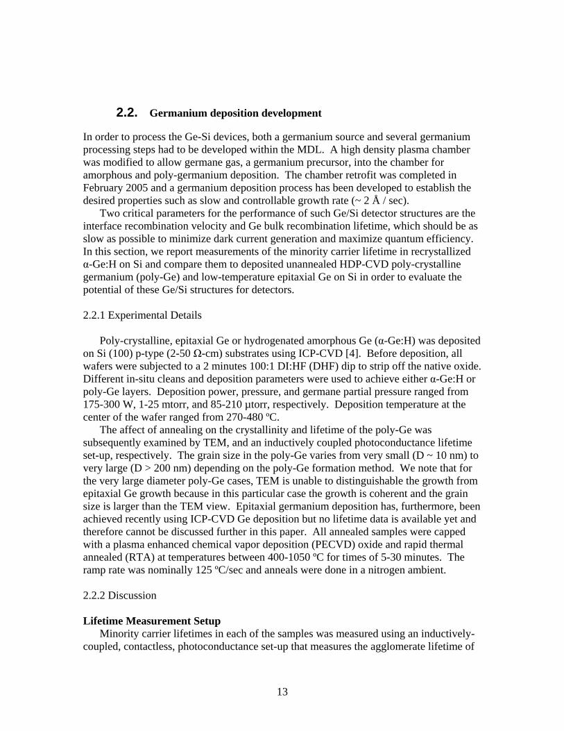
Minority carrier lifetimes in each of the samples was measured using an inductively-coupled, contactless, photoconductance set-up that measures the agglomerate lifetime of
14
the bulk Si, heterostructure and surfaces. The lifetime measurement setup utilizes a common technique based on the photoconductance decay transients after a short light pulse from a strobe lamp, Fig. 2.2.1.
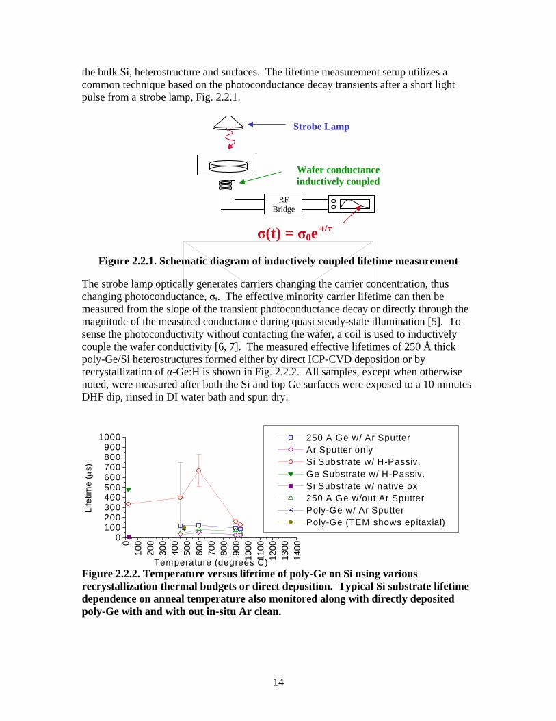
Figure 2.2.1. Schematic diagram of inductively coupled lifetime measurement The strobe lamp optically generates carriers changing the carrier concentration, thus changing photoconductance, σt. The effective minority carrier lifetime can then be measured from the slope of the transient photoconductance decay or directly through the magnitude of the measured conductance during quasi steady-state illumination [5]. To sense the photoconductivity without contacting the wafer, a coil is used to inductively couple the wafer conductivity [6, 7]. The measured effective lifetimes of 250 Å thick poly-Ge/Si heterostructures formed either by direct ICP-CVD deposition or by recrystallization of α-Ge:H is shown in Fig. 2.2.2. All samples, except when otherwise noted, were measured after both the Si and top Ge surfaces were exposed to a 10 minutes DHF dip, rinsed in DI water bath and spun dry.
010
020
030
040
050
060
070
080
090
010
0011
0012
0013
0014
00
0100200300400500600700800900
1000 250 A Ge w/ Ar Sputter Ar Sputter only Si Substrate w/ H-Passiv. Ge Substrate w/ H-Passiv. Si Substrate w/ native ox 250 A Ge w/out Ar Sputter Poly-Ge w/ Ar Sputter Poly-Ge (TEM shows epitaxial)
Life
time
(µs)
Temperature (degrees C) Figure 2.2.2. Temperature versus lifetime of poly-Ge on Si using various recrystallization thermal budgets or direct deposition. Typical Si substrate lifetime dependence on anneal temperature also monitored along with directly deposited poly-Ge with and with out in-situ Ar clean.
RFBridge
Strobe Lamp
Wafer conductanceinductively coupled
σ(t) = σ0e-t/τ
15
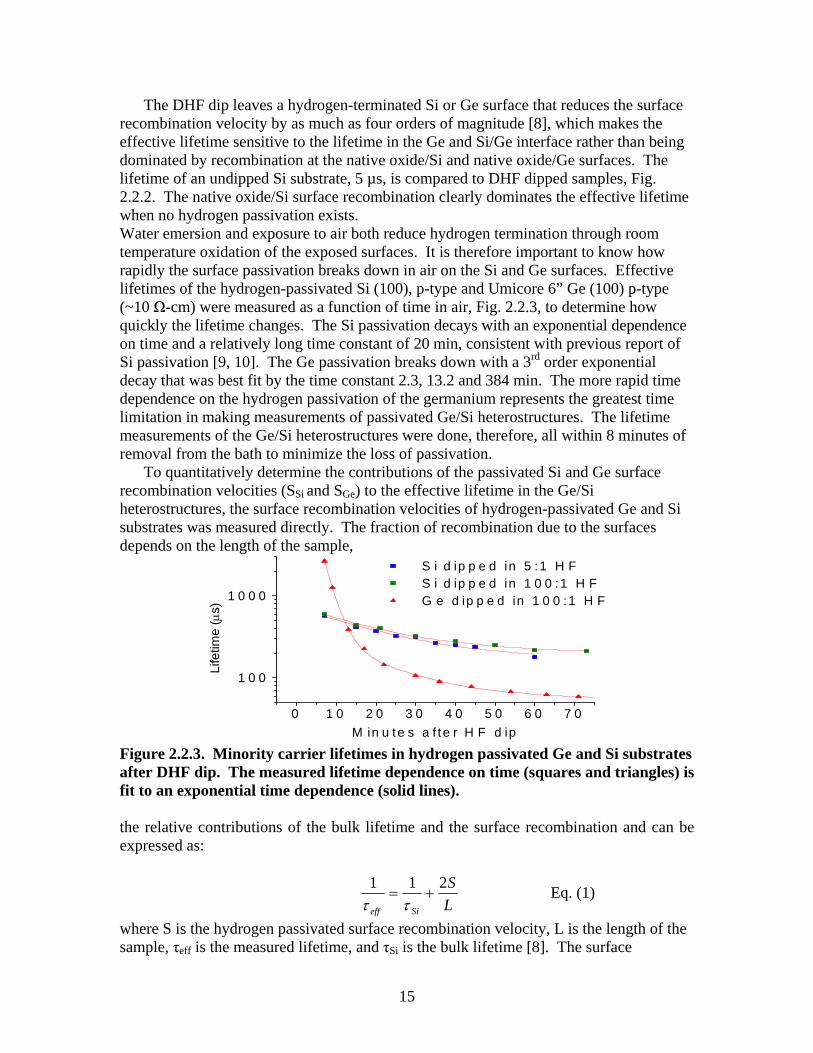
The DHF dip leaves a hydrogen-terminated Si or Ge surface that reduces the surface recombination velocity by as much as four orders of magnitude [8], which makes the effective lifetime sensitive to the lifetime in the Ge and Si/Ge interface rather than being dominated by recombination at the native oxide/Si and native oxide/Ge surfaces. The lifetime of an undipped Si substrate, 5 µs, is compared to DHF dipped samples, Fig. 2.2.2. The native oxide/Si surface recombination clearly dominates the effective lifetime when no hydrogen passivation exists. Water emersion and exposure to air both reduce hydrogen termination through room temperature oxidation of the exposed surfaces. It is therefore important to know how rapidly the surface passivation breaks down in air on the Si and Ge surfaces. Effective lifetimes of the hydrogen-passivated Si (100), p-type and Umicore 6” Ge (100) p-type (~10 Ω-cm) were measured as a function of time in air, Fig. 2.2.3, to determine how quickly the lifetime changes. The Si passivation decays with an exponential dependence on time and a relatively long time constant of 20 min, consistent with previous report of Si passivation [9, 10]. The Ge passivation breaks down with a 3rd order exponential decay that was best fit by the time constant 2.3, 13.2 and 384 min. The more rapid time dependence on the hydrogen passivation of the germanium represents the greatest time limitation in making measurements of passivated Ge/Si heterostructures. The lifetime measurements of the Ge/Si heterostructures were done, therefore, all within 8 minutes of removal from the bath to minimize the loss of passivation.
To quantitatively determine the contributions of the passivated Si and Ge surface recombination velocities (SSi and SGe) to the effective lifetime in the Ge/Si heterostructures, the surface recombination velocities of hydrogen-passivated Ge and Si substrates was measured directly. The fraction of recombination due to the surfaces depends on the length of the sample,
0 1 0 2 0 3 0 4 0 5 0 6 0 7 0
1 0 0
1 0 0 0
S i d ip p e d in 5 :1 H F S i d ip p e d in 1 0 0 :1 H F G e d ip p e d in 1 0 0 :1 H F
Life
time
(µs)
M in u te s a f te r H F d ip Figure 2.2.3. Minority carrier lifetimes in hydrogen passivated Ge and Si substrates after DHF dip. The measured lifetime dependence on time (squares and triangles) is fit to an exponential time dependence (solid lines). the relative contributions of the bulk lifetime and the surface recombination and can be expressed as:
LS
Sieff
211+=
ττ Eq. (1)
where S is the hydrogen passivated surface recombination velocity, L is the length of the sample, τeff is the measured lifetime, and τSi is the bulk lifetime [8]. The surface

16
recombination velocity may be extracted if the effective lifetime is measured for the same sample for different thicknesses. The Ge substrate was, therefore, etched using hydrogen peroxide (H2O2), and a dry etch was used for the Si. Surface recombination velocities of 4.2 ± 2 cm/s, 5.8 ± 2 cm/s and a bulk recombination of 7.0 ± 4 ms, 514 ± 20 µs were found for Ge and Si respectively. The uncertainty of the measurements of the SGe and Ge bulk recombination due to the time dependence of the hydrogen passivation is estimated to be ± 17 %.
Quantitative Measurement of Seff for different Poly-Ge/Si
The measured effective lifetime for the poly-Ge/Si samples is a combination of surface, interface, and bulk recombination in the bulk of the materials and at their respective boundaries. To quantify the increased recombination due to the addition of the poly-Ge layer, the agglomerate recombination due to the poly-Ge layer may be viewed as an effective surface recombination velocity at one side of the Si substrate, Seff:
1τeff
1τSi
SSi
L+
Seff
L+
Eq. (2) where, Seff is the effective surface recombination velocity at the Ge/Si edge, and SSi is the Si surface recombination velocity. Seff therefore represents the combined recombination contributions of the (1) Ge/Si interface, (2) Ge bulk, and (3) Ge/air surface.
The recombination velocities show a range between 2x10³ - 2x104 cm/s depending on the method of poly-Ge formation. A clear decrease in recombination for all temperatures is observed when the in-situ argon sputtering step is added. Incomplete cleaning before epitaxy, which leaves residual contamination like oxygen and carbon, is known to increase defect density and lower lifetimes [11], therefore, the reduction of recombination through the introduction of an in-situ clean before deposition and recrystallization is not surprising. However, we note that other effects due to the presence of an underlying amorphized silicon layer that might beneficially reduce recombination can not
400 500 600 700 800 900 1000
103
104 Poly-Ge w/ Ar Sputter 250A Ge w/ Ar Sputter Large grain poly coherently
oriented to the substrate 250A Ge w/out Ar sputter
S_e
ff (c
m/s
)
Temperature (degrees C)
Figure 2.2.4. The calculated effective surface recombination velocities at the poly-Ge/Si interface for poly-Ge directly deposited compared to recrystallized a-Ge:H at varying temperatures.
17
Ge
SiGe
Si
Ge
Si(a) (b) (c)
be ruled out since it is not clear how the amorphized silicon layer impacts the growth and subsequent quality of the recrystallized Ge layer.
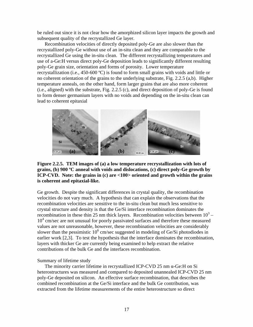
Recombination velocities of directly deposited poly-Ge are also slower than the recrystallized poly-Ge without use of an in-situ clean and they are comparable to the recrystallized Ge using the in-situ clean. The different recrystallizing temperatures and use of a-Ge:H versus direct poly-Ge deposition leads to significantly different resulting poly-Ge grain size, orientation and forms of porosity. Lower temperature recrystallization (i.e., 450-600 ºC) is found to form small grains with voids and little or no coherent orientation of the grains to the underlying substrate, Fig. 2.2.5 (a,b). Higher temperature anneals, on the other hand, form larger grains that are also more coherent (i.e., aligned) with the substrate, Fig. 2.2.5 (c), and direct deposition of poly-Ge is found to form denser germanium layers with no voids and depending on the in-situ clean can lead to coherent epitaxial
Figure 2.2.5. TEM images of (a) a low temperature recrystallization with lots of grains, (b) 900 ºC anneal with voids and dislocations, (c) direct poly-Ge growth by ICP-CVD. Note: the grains in (c) are <100> oriented and growth within the grains is coherent and epitaxial-like. Ge growth. Despite the significant differences in crystal quality, the recombination velocities do not vary much. A hypothesis that can explain the observations that the recombination velocities are sensitive to the in-situ clean but much less sensitive to crystal structure and density is that the Ge/Si interface recombination dominates the recombination in these thin 25 nm thick layers. Recombination velocities between 103 – 104 cm/sec are not unusual for poorly passivated surfaces and therefore these measured values are not unreasonable, however, these recombination velocities are considerably slower than the pessimistic 106 cm/sec suggested in modeling of Ge/Si photodiodes in earlier work [2,3]. To test the hypothesis that the interface dominates the recombination, layers with thicker Ge are currently being examined to help extract the relative contributions of the bulk Ge and the interfaces recombination. Summary of lifetime study
The minority carrier lifetime in recrystallized ICP-CVD 25 nm α-Ge:H on Si heterostructures was measured and compared to deposited unannealed ICP-CVD 25 nm poly-Ge deposited on silicon. An effective surface recombination, that describes the combined recombination at the Ge/Si interface and the bulk Ge contribution, was extracted from the lifetime measurements of the entire heterostructure so direct
18
comparison of recombination in germanium deposited with different deposition methods could be carried out. Little difference in recombination was observed between the different poly-Ge formation methods although the different methods of poly-Ge deposition produced varying grain size, density, voiding, and coherency with the underlying substrate. Despite the insensitivity of the recombination to differences in crystallinity, the introduction of an in-situ argon sputter clean uniformly reduced recombination at all recrystallization temperatures compared to samples without the sputter clean. The recombination velocity’s combined insensitivity to crystallinity and sensitivity to interface cleaning steps suggests that although the germanium can be extremely small poly grain, the interface recombination may still be the dominant contribution to recombination in the Ge/Si heterostructure. Finally, the magnitude of the recombination velocity in these structures is of order of 103-104 cm/sec, which is considerably less than 106 cm/sec used in previous estimates.
2.2.3 References [1] C. Masini, L. Calace, G. Assanto, H-C. Luan, L. C. Kimerling, IEEE Trans. Elec. Dev., 48, 1092 (2001) [2] S. Famà, L. Colace, G. Masini, G. Assanto, H.-C. Luan, Appl. Phys. Lett., 81, 586 (2002) [3] G. Masini, V. Cencelli, L. Colace, F. De Nortaristefani, G. Assanto, Appl. Phys. Lett., 80, 3268 (2002) [4] http://www.appliedmaterials.com/products/hdp_cvd_ultima.html?menuID=1_3_1 [5] R.A. Sinton, Testing Solar Cell Wafers After Phosphorus Diffusion, April 27, 2004 [6] D.E. Kane, R.M. Swanson, Proc. 18th IEEE Photovoltaic Specialist Conf., 578 (1985) [7] R.A. Sinton, A. Cuevas, Appl. Phys. Lett., 69, 2510 (1996) [8] E. Yablonovitch, D.L. Allara, C.C. Chang, T. Gmitter, T.B. Bright, Phys. Rev. Lett., 57, 249 (1986) [9] D. Gräf, M. Grundner, R. Schulz, L. Mühlhoff, J. Appl. Phys., 68, 5155 (1990) [10] A. Stockhausen, T.V. Kampen, W. Mönch, Appl. Surf. Sci., 56-5, 795 (1992) [11] M.S. Carroll, C. A. King, Thin Solid Films, 473, 173 (2005)

19
2.3. Germanium on Silicon Epitaxy Development
2.3.1 Background During the examination of lifetime dependence on different ways to form
crystalline germanium on the silicon, it was found that epitaxial germanium could be produced using the HDP-CVD. However the epitaxy was highly dislocated and it was unclear what role the surface preparation played in this. A common challenge to improving the germanium quality is the thermal budget of the in-situ bake, which is used to reduce defect forming oxygen and carbon surface residues [1, 2]. Typical cleaning temperatures to remove significant concentrations of oxygen and carbon have been reported to be approximately 750ºC for thermal hydrogen bakes in standard chemical vapor deposition chambers [3]. Germanium device performance using lower peak in-situ cleans (i.e., ~450°C) has been hampered by additional crystal defectivity, although epitaxy is possible with out complete removal of oxygen and carbon at lower temperatures [4]. However, for the MDL HDP-CVD the temperature of the substrate is limited to plasma heating limiting peak temperatures to ~500°C without applying additional self-bias that produces considerable damage due to ion bombardment. Therefore, thermal desorption of oxygen and carbon is not possible.
Nevertheless, plasma enhanced chemical vapor deposition (PECVD) can be used to reduce the processing temperature. Hydrogen plasma assisted in-situ surface preparation of epitaxy has been shown to reduce both carbon and oxygen concentrations and enable epitaxial growth at temperatures as low as ~150°C [5, 6]. The hydrogen is believed to help produce volatile Si-O and H2O species in the removal of oxygen, although typically this is not reported to occur rapidly enough to completely clear the surface of all oxygen until ~550ºC.
In this section, we describe the use of an in-situ argon/germane high density plasma to help initiate germanium epitaxy on silicon using a peak temperature of approximately 460ºC. Germanium is believed to readily break Si-O bonds to form more volatile Ge-O [7-9], therefore, argon/germane plasmas offer the potential to reduce the necessary in-situ clean temperature while obtaining similar results as hydrogen in-situ cleans. To the authors knowledge this report is also the first demonstration of germanium epitaxy on silicon using this commercially available high density plasma chamber configuration instead of, for example, remote or electron cyclotron resonance configurations. A further motivation to pursue this form of Ge on Si growth, despite the high dislocation density, is recently reported Ge (p)/Si (n) diodes that include the interface in the junction were reported to produce detectors with potentially useful NIR performance despite the defective interface (e.g. Jd ~ 10 mA/cm-2, and responsivity as high as 0.59 A/W, at 1550 nm) [11]. Most if not all reported low temperature (T < 450ºC) Ge detectors have used either e-beam evaporation (i.e., in some cases polycrystalline Ge, or molecular beam epitaxy (MBE)) [4, 12]. Improvement upon these results using a more commercially

20
standard deposition technique while maintaining the low deposition temperature would be desirable. 2.3.2 Experiment & Discussion
Germanium was deposited on Si (100) p-type (2-10 Ω-cm) substrates using HDP-CVD. The HDP-CVD used in this work is a commercially available chamber typically used for high density plasma chemical vapor deposition of oxides [13] that was modified so that a germane/argon mixture (1% germane in argon) could be injected for SiGe deposition. Unless otherwise noted all wafers received a 1 minutes 100:1 DI:HF (DHF) dip to strip off the native oxide. Different in-situ cleans and deposition parameters were used to achieve either amorphous, poly-Ge or single crystal Ge epitaxy. For this work the deposition power, pressure, and germane partial pressure ranged from 1000-5000 W, 1-25 mtorr, and 10-85 µtorr, respectively. Deposition temperature at the center of the wafer depended directly on applied power to the argon/germane plasma and ranged from 250-550ºC. A transition from amorphous to poly-Ge deposition was observed with increasing power and temperature, Fig. 2.3.1. The solid-phase epitaxial recrystallization rates of amorphous germanium approach the deposition rate (~1-3 Å/sec) at between 350 and 400ºC [14]. Thermally assisted motion of the atoms in the surface and near surface region may therefore be sufficient to explain the transition from amorphous to the crystalline phase of the growth at these increased powers.
To establish the crystallinity the films were measured initially with X-ray diffraction. Ellipsometry of the films was also used to rapidly evaluate films using the goodness of fit to either a hydrogenated amorphous germanium model or a single crystal germanium model. It was found that increasing coherency of the germanium single crystal with the substrate, estimated using the ratio of misaligned to <100> diffraction peak intensity to coherently aligned intensity, was found to correlate with increasingly close fits to the germanium single crystal model. Representative samples were also examined using TEM to unambiguously determine the crystallinity and defect density (i.e., threading dislocation density) of the films.
Figure 2.3.1. Substrate temperature dependence of HDP-CVD germanium films on applied power. A transition from amorphous to poly-Ge was observed at powers of 2000W and above. An additional low pressure in-situ surface preparation step was necessary to assist in the formation of single crystal epitaxy instead of poly-Ge.
0 1000 2000 3000 4000 5000250
300
350
400
450
500poly-Ge
Subs
trate
Tem
pera
ture
[Cel
sius
]
Power [Watts]
a-Ge

21
0 100 200 300 400 500 6001012
1013
1014
1015
1016
Oxygen Carbon
Are
al D
ensi
ty [c
m-2
]
Time [seconds]0 5 10 15 20-0.5
0.0
0.5
1.0
1.5
2.0
2.5
3.0
3.5
Ge
Dep
ositi
on R
ate
[A/s
ec]
Pressure [mtorr]
Oxi
de R
emov
al
Ge Deposition
Power = 3000 WPGeH4
~ 0.01 PTotal
?
Secondary ion mass spectrometry (SIMS) and Rutherford backscattering (RBS)
measurements were also done on some samples to determine the chemical composition of the films as well as characterizing oxygen and carbon residue at the Ge/Si interfaces, Fig. 2.3.2. Amorphous films contained approximately 3% hydrogen, while crystalline films showed hydrogen contents well below the detection limits of RBS. Oxygen and carbon concentrations were found to be ≥1019 cm-3 and 1017 cm-3 within the films, respectively. A necessary requirement to initiate germanium epitaxy is that the crystal template of the silicon surface have oxygen and carbon free areas at which the germanium atoms can coherently attach to the silicon atomic lattice sites. It is well known that silicon surfaces can be prepared with relatively low oxygen free hydrogen terminated surfaces through use of an ex-situ HF dips, which is sufficient for thermal CVD systems to grow relatively defect free epitaxy although oxygen and carbon are always found at the substrate growth interface using HF dips only. On the other hand, standard HF dips are not usually sufficiently stable to allow epitaxial growth in plasma systems despite the much lower peak temperatures [15]. All germanium deposited in this work was found to be polycrystalline when using HF dips followed by directly depositing germanium, which included an initial warm-up step of several minutes in the presence of a 3000W, 10 mtorr (or 1 mtorr) argon plasma followed by introducing 50 µtorr of germane to initiate the Ge deposition once the substrate reached it’s steady-state temperature of 460°C. This is consistent with previous reports of plasma assisted epitaxial growth, which typically required an in-situ surface preparation step like a hydrogen plasma clean [15].
(a) (b) Figure 2.3.2 (a) germanium deposition rate dependence on total pressure in plasma chamber (negative values represent the measured oxide removal rate); and (b) areal density of oxygen and carbon observed at the Ge/Si interface after different times of 1 mtorr, Ar/GeH4 plasma surface preparation before Ge deposition.
Typical plasma cleans rely on hydrogen to assist the formation of volatile silicon oxide and steam from the surface [16].
22
#6981
poly-Ge
c-Si
Amorphousinterface
SiO2 + 2H → SiO(g) + H2O eqn. 1 However, hydrogen plasma cleans require substrate temperature of approximately 550°C or higher to completely remove the oxygen [6]. A reduction in in-situ clean temperature of approximately 100°C is desired to allow for deposition of germanium after all CMOS fabrication is completed (i.e., metal is deposited). Germanium oxide is known to be volatile at considerably lower temperatures than silicon oxide and is reported to readily break existing Si-O bonds [7-9]. The introduction of germane at low fluxes offers a potential way to reduce the temperature at which oxide may be removed from the silicon surface.
Deposition rate at a fixed power and substrate temperature was found to depend on plasma pressure. A transition from germanium deposition to oxide removal was subsequently observed when the argon/germane plasma pressure dropped to 1 mtorr, Fig 2.3.2. The dependence of deposition rate on pressure in the inductively coupled plasma is likely due to an increase in electron temperature, which results in both an increase in sheath potential and a sub-linear reduction in ion density. We speculate that a low energy sputtering component, due to the increased sheath potential, suppresses germanium deposition and ion assisted Ge and H bombardment of the Si surface leads to Si-O, Ge-O and HxO desorption. The reduction in carbon in the presence of hydrogen ions is very rapid even at T ~ 350°C [3, 16].
The oxygen removing plasma condition at 1 mtorr was subsequently found to assist in initiating single crystal germanium epitaxy on silicon when the step was introduced directly before the deposition and after the plasma warm-up step. This is in contrast with the repeatable formation of poly-Ge when germane is removed from the 1 mtorr surface preparation step (i.e., a 1 mtorr argon plasma does not lead to the formation of Ge epitaxy), Fig 2.3.3. Ge films deposited using alternative in-situ surface preparation steps before the deposition, like exposing the surface to reactive NF3 species from a remote plasma source, also resulted in poly-Ge films.
Ge SiOx (a) (b) Figure 2.3.3 (a) TEM of Ge deposited on Si using a 1 mtorr argon plasma surface preparation step followed by the standard 10 mtorr Ge deposition step and (b) HRTEM of epitaxial germanium that results after germane is inserted into the 1
23
mtorr surface preparation step. Epitaxy grows through windows in amorphous regions at the Ge/Si interface.
A combination of XRD, ellipsometry and TEM confirm that the germanium crystal growth is coherent (i.e., <100> oriented) and epitaxial over the entire surface. TEM shows, furthermore, a large frequency of amorphous regions at the Ge/Si interface. High resolution TEM shows that the germanium crystal grows in between the amorphous regions and coalesces above the interface region as coherently aligned (100) crystal. A large concentration of oxygen is observed at the Ge/Si interface by SIMS, Fig. 2.3.3 (b), which suggests that the amorphous regions observed in TEM is residual oxide. Germanium epitaxy grown in nanowindows of the oxide has been reported before and when the size and spacing of the windows is tuned properly, this can also result in significantly reduced dislocation density [7, 17]. A large number of threading dislocations (~1010 cm-2) is observed in this case, which is not atypical for germanium epitaxy on silicon when no special steps are taken (e.g., graded buffer layers or tuned nanowindow formation [17]).
Finally, the reduction of oxygen and carbon at 460°C is similar if not better than what has been reported for electron cyclotron resonance (ECR) hydrogen plasmas using similar total pressures, 1 mtorr, greater hydrogen partial pressures and temperatures constrained to below 550°C. Further investigation is proceeding to unambiguously clarify whether there is an enhanced removal of oxygen due to the presence of germanium or alternatively whether the oxygen and carbon reduction at the surface is only due to dissociated hydrogen from the germane molecules. 2.3.3 Summary of results Low temperature (~460°C) germanium epitaxy was grown using a commercially available high density plasma chemical vapor deposition (HDP-CVD) chamber. To the authors knowledge this is the first report of Ge on Si epitaxy using this particular plasma chamber configuration. Furthermore, to assist in the growth of low temperature epitaxy we describe an alternative in-situ surface preparation step using a 1 mtorr, 3000W, 460°C argon/germane plasma that reduces oxygen and carbon concentration from the silicon surface and enables epitaxial growth. Introduction of germanium to form Ge-O volatile compounds to assist in reducing the temperature at which oxygen may be removed from the surface motivates this examination of germane/argon plasmas for low-temperature in-situ cleaning so that higher quality Ge on Si epitaxy may be formed for the Ge/Si APDs. 2.3.4 References [1] K. Oda and Y. Kiyota, J. Electrochem. Soc., vol. 143, pp. 2361, 1996. [2] M. S. Carroll and C. A. King, Thin Solid Films, vol. 473, pp. 137, 2003. [3] A. Crossley, et al., Vacuum, vol. 46, pp. 667, 1995. [4] P. R. Bandaru, et al. Material Science and Engineering B, vol. 113, pp. 79-84, 2004. [5] H.-W. Kim and R. Reif, Thin Solid FIlms, vol. 289, pp. 192-198, 1996. [6] H.-S. Tae, et al. Applied Physics Letters, vol. 64, pp. 1021, 1993. [7] C.-L. Wang, et al. J. Electrochem. Soc., vol. 143, pp. 2387, 1996. [8] J. F. Morar, et al. Appl. Phys. Lett., vol. 50, pp. 463, 1986.

24
[9] M. M. Moslehi, SPIE - Rapid Thermal and Related Processing Techniques, vol. 1393, pp. 90, 1990.
[10] Y.-H. Kuo, et al. Nature, vol. 437, pp. 1334, 2005. [11] J. Liu, et al. Applied Physics Letters, vol. 87, pp. 103501, 2005. [12] G. Masini, et al., Applied Physics Letters, vol. 80, pp. 3268, 2002. [13] Applied-Materials, High Density Plasma Chemical Vapor Deposition Chamber
(Centura) [14] L. Csepregi, et al., Solid State Communications, vol. 21, pp. 1019-1021, 1977. [15] S. Reidy, et al., J. of Vac. Sci. Tech. B, vol. 21, pp. 970, 2003. [16] H.-W. Kim, "Wafer Surface Cleaning for Silicon Homoepitaxy with and without
ECR Hydrogen Plasma Exposure," in Materials Science and Engineering. Ph.D. Thesis, Massachusetts Institute of Technology, 1994. [17] Q. Li, et al., Applied Physics Letters, vol. 83, pp. 5032, 2003.
25
2.4. Germanium-Silicon Device Fabrication
2.4.1 Overview of process flow A process flow for the Ge-Si APD was developed and included a number of new steps for the silicon fabrication facility at Sandia National Labs, Figure 2.4.1. This included material contamination studies to establish what parts of the CMOS line could be exposed to the new Ge deposition process as well as the development of new process steps including: (1) integration of the new Ge deposition into an oxide window; (2) Ge island formation (i.e., Ge etch selective to oxide); (3) oxide etch selective to germanium; and (4) ohmic contact formation to the p-type germanium island.
Substrate
BOX (4000 )A
N+ (As, 5E19 ); 8 mµ
P-epi (B, 1E15 ); 4000 A
Nitride Pad (2500 )A
(1)
(2)
Trench Isolation
Silicon Implant & ActivationSubstrate
BOX (4000 )
N+ (As, 5E19 ); 8 um
P N+P-
A
Thermal Oxide: 500 A
Substrate
BOX (4000 )N+ (As, 5E19 ); 8mµ
P N+P-
A
Oxide: 500-1000AGe: 4000 A
Metalization
Substrate
BOX (4000 )N+ (As, 5E19 ); 8um
P N+P-
A
Ge: 4000 A
ILDOxide: 500-1000A
Ge Deposition, Implant &Dry Etch
(1) Etch oxide stop on Ge(2) Form metal contact
(1) Etch Ge Island stop on oxideor silicon
(3)
(4)
Figure 2.4.1, Abbreviated process flow for the Ge/Si APD. Selective dry etching was developed using standard silicon based chemistries relatively rapidly and resulted in very good selectivity between oxide and germanium as can be seen in, Fig 2.4.2 (a), a scanning electron micrograph of Ge islands and the beginning formation of the metallization vias. Germanium deposition over an oxide window was however found to create circular defects predominantly at the oxide/Si/Ge edges. The geometric dependence of the defects suggests a stress related effect because the defects are not observed either on blanket oxides or silicon. Because surface generation at the silicon surface was expected to produce a minor contribution in dark current to the Ge/Si APD, the oxide was stripped in the process flow and germanium was deposited directly on the silicon substrate. The Ge/Si interface and defects in the germanium are the dominant sources of the dark current in this device, therefore, less ideal oxide termination of the silicon surface with plasma assisted oxide is not believed to represent a significant problem for this device.
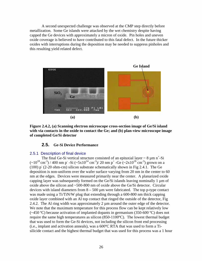
26
SiO2
Si
Ge
Ge Island
A second unexpected challenge was observed at the CMP step directly before metallization. Some Ge islands were attacked by the wet chemistry despite having capped the Ge devices with approximately a micron of oxide. Pin holes and uneven oxide coverage is believed to have contributed to this fatal defect. In the future thicker oxides with interruptions during the deposition may be needed to suppress pinholes and this resulting yield related defect. (a) (b) Figure 2.4.2, (a) Scanning electron microscope cross-section image of Ge/Si island with via contacts in the oxide to contact the Ge; and (b) plan-view microscope image of completed Ge/Si detector
2.5. Ge-Si Device Performance
2.5.1 Description of final device The final Ge-Si vertical structure consisted of an epitaxial layer ~ 8 µm n+-Si
(~1018 cm-3) / 400 nm p- -Si (~5x1014 cm-3)/ 20 nm p+ -Ge (~2x1018 cm-3) grown on a (100) p- (2-20 ohm-cm) silicon substrate schematically shown in Fig 2.4.1. The Ge deposition is non-uniform over the wafer surface varying from 20 nm in the center to 60 nm at the edges. Devices were measured primarily near the center. A planarized oxide capping layer was subsequently formed on the Ge/Si islands leaving nominally 1 µm of oxide above the silicon and ~500-800 nm of oxide above the Ge/Si detector. Circular devices with island diameters from 8 – 500 µm were fabricated. The top p-type contact was made using a Ti/TiN/W plug that extending through a 600-800 nm thick capping oxide layer combined with an Al top contact that ringed the outside of the detector, Fig 2.4.2. The Al ring width was approximately 2 µm around the outer edge of the detector. We note that the maximum temperature for this process flow can be kept relatively low (~450 ºC) because activation of implanted dopants in germanium (350-600 ºC) does not require the same high temperatures as silicon (850-1100ºC). The lowest thermal budget that was used to form the Ge-Si devices, not including the silicon front end processing (i.e., implant and activation anneals), was a 600ºC RTA that was used to form a Ti-silicide contact and the highest thermal budget that was used for this process was a 1 hour

27
3530252015105010-11
10-10
10-9
10-8
10-7
10-6
10-5
R=10 umT=300KW7die89up27
no light 1550 nm
Cur
rent
[A]
Applied Bias [V]0 5 10 15 20 25 30 35
0
100
200
300
400
500
Ph
otoc
urre
nt M
ultip
lier
Applied Bias [Volts](a) (b)
Si
PunchThrough
700ºC anneal, which was used to improve defect annealing in the Ge. The significantly lower thermal budget used for germanium processing allows it to be inserted very late in the CMOS process flow making it significantly easier to integrate with standard VLSI technologies.
2.5.2 Room temperature I-V
Room temperature I-V measurements were made to characterize the dark current performance and optical response, Fig 2.4.3 (a) & (b). The current response of the Ge/Si device appears to have several different bias regions. At biases below approximately 3V the dark current is very low with respect to a germanium device and has no photoresponse. At biases above ~ 3V the 1550 nm photoresponse increases above the dark current by about an order of magnitude, which we designate as punch-through analogous to the behavior observed in InGaAs/InP APDs. With increasing bias between punch through to approximately 15V both the photoresponse and dark current increase by about 2-3 and a factor of 10 respectively. Beyond 15V both dark current and photoresponse increase rapidly and by approximately the same amount. The increase in the photoresponse is calculated in Fig 2.4.4 (b) as: Photomultiplier = (I – Idark)/Ipunch-through. Figure 2.4.3, (a) current dependence on voltage with and without 1550 nm illumination; and (b) relative increase in photocurrent at 5 V with increasing applied bias. One-dimensional device simulations were performed to better understand the dark current and photoresponse anticipated from the Ge-Si device structure, Fig 2.4.7 (a) & (b). The different bias regions of the diode, electron energy band diagrams are calculated for different biases. At low bias, 0V, the electron energy band diagram has a barrier for minority electron carrier transport from the Ge into the n-type silicon. The origin of this electron barrier comes from the combination of two barriers to electron transport between the p-Ge and n-Si. The primary barrier is the 500 nm p- Si between the n-Si and p-Ge. The second barrier is due to the abrupt band-offset between the Ge and Si combined with the Fermi level positions that are deterimined by the doping of the two materials.
28
-1.4 -1.2 -1.0 -0.8 -0.6 -0.4 -0.2 0.0 0.2-2
0
2
4
6
8
10
12
Elec
tron
Ener
gy [e
V]
Distance [um]05101520253035 10-13
10-1210-1110-1010-910-810-710-610-510-4
Cur
rent
[A]
Applied Bias [V]
Si epi 100 nmGe epi 40 nmQ=8e15 boronTau=10-8 sec
4V
0V
8V
12V
Small ResidualBarrier
Ge electron Minority carriers
Fully injected
Increasing SRHGeneration in Ge
Multiplication
(a) (b)
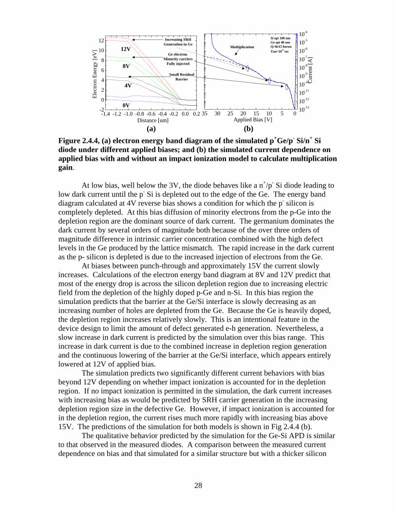
Figure 2.4.4, (a) electron energy band diagram of the simulated p+Ge/p- Si/n+ Si diode under different applied biases; and (b) the simulated current dependence on applied bias with and without an impact ionization model to calculate multiplication gain.
At low bias, well below the 3V, the diode behaves like a n+/p- Si diode leading to low dark current until the p- Si is depleted out to the edge of the Ge. The energy band diagram calculated at 4V reverse bias shows a condition for which the p- silicon is completely depleted. At this bias diffusion of minority electrons from the p-Ge into the depletion region are the dominant source of dark current. The germanium dominates the dark current by several orders of magnitude both because of the over three orders of magnitude difference in intrinsic carrier concentration combined with the high defect levels in the Ge produced by the lattice mismatch. The rapid increase in the dark current as the p- silicon is depleted is due to the increased injection of electrons from the Ge.
At biases between punch-through and approximately 15V the current slowly increases. Calculations of the electron energy band diagram at 8V and 12V predict that most of the energy drop is across the silicon depletion region due to increasing electric field from the depletion of the highly doped p-Ge and n-Si. In this bias region the simulation predicts that the barrier at the Ge/Si interface is slowly decreasing as an increasing number of holes are depleted from the Ge. Because the Ge is heavily doped, the depletion region increases relatively slowly. This is an intentional feature in the device design to limit the amount of defect generated e-h generation. Nevertheless, a slow increase in dark current is predicted by the simulation over this bias range. This increase in dark current is due to the combined increase in depletion region generation and the continuous lowering of the barrier at the Ge/Si interface, which appears entirely lowered at 12V of applied bias.
The simulation predicts two significantly different current behaviors with bias beyond 12V depending on whether impact ionization is accounted for in the depletion region. If no impact ionization is permitted in the simulation, the dark current increases with increasing bias as would be predicted by SRH carrier generation in the increasing depletion region size in the defective Ge. However, if impact ionization is accounted for in the depletion region, the current rises much more rapidly with increasing bias above 15V. The predictions of the simulation for both models is shown in Fig 2.4.4 (b).
The qualitative behavior predicted by the simulation for the Ge-Si APD is similar to that observed in the measured diodes. A comparison between the measured current dependence on bias and that simulated for a similar structure but with a thicker silicon

29
05101520253035 10-1410-1310-1210-1110-1010-910-810-710-610-510-4
Tau=1e-9
Tau=1e-7
Cur
rent
[A]
Applied Bias [V]
Si epi 100 nmGe epi 40 nmQ=8e15 boron
epitaxy layer is shown in Figure 2.4.5. The simulation was done for three different minority carrier lifetimes in the Ge to illustrate the predicted current dependence on defectivity of the germanium. Measurements of minority carrier lifetimes in e-beam deposited poly-Ge on silicon are reported to be approximately 5 ns [1], while state-of-the-art epitaxial Ge grown on silicon using graded buffer layers or cyclic annealing, for example, have much lower defect densities and therefore longer lifetimes that in principle would approach bulk crystal on the order of 1 ms. Qualitatively, the measured dark current behavior is very similar to the simulated. The more rapid increase in dark current at low bias is likely because the simulation is done for a thicker p- region therefore more bias is required to deplete out the region than is actually present in the measured diode. The commencement of impact ionization is difficult to predict accurately without a well calibrated model, however, by coincidence for the silicon thickness simulated in this case, the breakdown voltage is not far from the observed case. Comparing the dark current density to that predicted from the different lifetimes brackets the lifetime in the germanium to be between 10-7 and 10-9 seconds, which is better than that expected from the poly-Ge case [1] and much better than the 10-100 ps suggested by Bandaru et al. [2]. However, this estimate relies on assumptions about the active hole concentration in the Ge, the conduction band offset, and that the interface generation is not as great as the generation coming from the depleted, defective, germanium. Nevertheless, if this device structure was built with more state-of-the-art Ge on silicon approaches like cyclic annealing [3], the lifetimes would be considerably longer and overall performance of the device would be expected to increase considerably at higher biases. At biases just beyond punch-through, the dark currents are as good or slightly better (~0.1 mA/cm2) compared to that reported for Ge diodes built on silicon that range between 0.1 – 10 mA/cm2. Assuming that the simulated model is accurately describing the physics of the Ge/Si diode, the low dark currents can be attributed to the highly doped Ge that, suppresses the size of the depletion region in the highly defect Ge, produces a residual barrier to electron transport, and that maintains a low electron minority carrier concentration available to inject into the silicon depletion region. Figure 2.4.5, comparison of measured current dependence on bias with simulated current dependence on bias for three different minority carrier lifetimes in the Ge.

30
0.0 1.0x10⁻⁵ 2.0x10⁻⁵
2x10⁻¹⁰
4x10⁻¹⁰
6x10⁻¹⁰
8x10⁻¹⁰
1x10⁻⁹
4.5x10⁻⁵ A/W
Dark Current Floor
Phot
ocur
rent
[A]
Estimated Power at 1550 nm [W]
2.5.3 Responsivity The responsivity of the Ge-Si APD was measured at varying intensities and a linear response was observed over a wide range, Fig 2.4.6 (a). Linearity in response is an indication that non-linear effects like Auger recombination are negligible. A responsivity at 1550 nm of 4.5x10⁻⁵ A/W was extracted from the measurement, which corresponds to an external quantum efficiency of the order of 0.01%. Several identifiable factors contribute to the low responsivity in this device including a thin absorption region (assumed to be 200 nm) and poor anti-reflection coating (R~ 0.5). The fraction of absorbed light at 1550 nm is calculated to be 4x10⁻³ (0.4%) of the total light when accounting for the combination of these two factors. Using this value, an internal quantum efficiency of the Ge-Si diode is estimated to be ~ 1%. The internal quantum efficiency is used in this discussion to indicate the fraction of electrons collected from electron-hole pairs that are produced in the thin absorbing region. A multi-layer stack, air/oxide/Ge/Si/air, was used to calculate the reflection coefficient for the stack and the absorption coefficient of single crystal Ge was used to estimate the fraction of absorbed light in the Ge [4]. Figure 2.4.6 (a) photocurrent dependence on estimated 1550 nm power incident on the Ge-Si APD. The responsivity is low in part because of a very thin absorbing layer.
In the initial design of the Ge-Si APD, a quantum efficiency well below 50% was anticipated for two primary reasons: non-ideal surface passivation and short recombination lifetimes within the Ge. Assuming that the surface and ohmic contact is a high recombination velocity region, as much as 50% of the electrons generated by the absorbed light will diffuse away from the detecting junction and will be lost. Furthermore, those electrons diffusing towards the junction must reach the depletion region edge before they recombine with a hole in the bulk germanium. The diffusion length before recombination, therefore, must be large compared to the thickness of the absorbing region to collect a large fraction of the remaining 50% of the carriers. Alternatively the fraction of collected electrons may be quantitatively modeled as a ratio of the time to reach the junction compared to the recombination lifetime:
31
From the comparison of experiment to simulation for current dependence on bias, we estimate that the recombination lifetime in the bulk germanium is of the order of 1 to 10 ns. An order of magnitude estimate for the average time for an electron to reach the junction depletion region edge can be made using classic random walk theory (i.e., τjunction ~ L2 / Delec). Although the diffusivity in this material is not known, electron mobilities in highly dislocate p-type Ge (1017 cm-3) have been reported to be ~100 cm2 /V-sec [2]. Using this mobility, the time to reach the junction through a 200 nm thick layer would be 1-2 ns. This time is of the same order as the bulk lifetime extracted from simulation but not sufficiently long to explain the 1% internal quantum efficiency.
Two hypothesis that would explain a lower internal quantum efficiency than anticipated from the previous calculations are (1) that the time to reach the junction is much longer than estimated (e.g., the diffusivity is slower due to traps from the dislocations or an energy barrier) or (2) the absorption is weaker than expected because significant SiGe alloying is produced during the thermal annealing. A pulse probe measurement is planned to characterize the diffusion time for electrons out of the Ge. We are also hoping to characterize the chemical profile with a SIMS measurement. In either case, the use of state-of-the-art epitaxial techniques would significantly reduce the dislocation density (i.e., higher diffusivity and longer bulk lifetimes). Although thicker layers were not used in this initial effort because the integration is slightly more challenging, thicker layers are relatively straight forward to develop. Therefore, it is reasonable that higher responsivities and internal quantum efficiencies can be expected with further development of this structure.
2.5.4 Performance at reduced temperature The Ge-Si APDs were also measured at reduced temperatures to both provide further insight into the physics of the Ge-Si APD and examine its potential for high performance signal to noise imaging. As the temperature is reduced from room temperature the dark current between the punch-through bias and ~10V drops to the background noise level of the keithley ammeter rapidly, Fig 2.4.7 (a). Photocurrent in this bias range shows a smaller temperature dependence consistent with previously reported temperature dependence of absorption in germanium. The photocurrent measurements were done at 1310 nm to reduce the temperature dependence of absorption that is strongly prevalent for 1550 nm, which is near the bandgap energy and is therefore very sensitive to the temperature dependence of the bandgap. The punch through bias stays nearly constant over the entire temperature range and the breakdown voltage decreases with reduced temperature. These observations are consistent with Ge-Si model already described.
junctionbulk
bulkFττ
τ+
=

32
0 5 10 15 20 2510-11
10-10
10-9
10-8
10-7
10-6
T=300K T=204K T=100K T=70K
Curre
nt [A
]
Bias [Voltage]0 5 10 15 20 25 3010-12
10-11
10-10
10-9
10-8
10-7
10-6
T=300K T=300K w/ 1310 nm T=210K w/ 1310 nm T=210K
Cur
rent
[A]
Bias [Voltage](a) (b)
Figure 2.4.7 (a) dark current dependence on bias and temperature; and (b) 1310 nm photoresponse dependence on bias and temperature.
At lower temperatures and higher biases, between ~19-22V, the dark current becomes relatively temperature insensitive. The dependence of the current on bias suggest that a band-to-band or trap assisted tunneling component begins to dominate at these temperatures and biases. A number of devices were tested and it was found that the bias at which the tunneling current dominates varies considerably both from device to device and also with peak annealing temperature after the Ge was deposited. This suggests that the tunneling mechanism is defect or process related. Considering the number of oxide/Si/Ge defects observed at the interface of the HDP-CVD deposited Ge (observed with TEM and SIMS), a likely candidate is mid-gap states at the interface. Low oxygen interfaces between Ge and Si are routinely achieved by CVD so it is likely that future devices fabricated with a better in-situ clean would further suppress this dark current component. Two characteristics of the I-V that are still not well understood are (1) the observed negative resistance near punch-through and (2) the weak temperature dependence of the dark current at biases below punch-through. The current Ge-Si model does not predict either of these effects. 2.5.5 Geiger mode operation of Ge-Si APD
To better understand the nature of the defects in the Ge-Si APD, the detectors were also tested in Geiger mode. Geiger mode performance is very sensitive to defects in the junction and can be used to characterize whether the trap is a majority or minority carrier as well as trapping times and trap cross sections. Furthermore, Geiger mode operation is insensitive to parasitic effects like shunt resistances making it a useful way to distinguish between intrinsic and extrinsic properties of the diode. A second motivation to examine these detectors in Geiger mode is due to recent work on fusion bonded InGaAs/Si APDs that demonstrated some potential advantages to operating lattice mismatched heterojunction APDs in Geiger mode and showed that the defect rich interface between the InGaAs and the silicon does not detrimentally overwhelm the Geiger mode performance making them potentially competitive with InGaAs/InP detectors. We were therefore interested in investigating what impact the defects in the Ge-Si device had on Geiger mode performance.

33
(a) (b)
Oscilloscope
Delay Pulse Generator
Pulse Generator Time Interval Ctr.
Photon Counter
CGate
50 Ohm
Variable Attenuator
Load R
DC Bias
NIR emitter
Geiger mode operation of an APD consists of operating the APD above the breakdown voltage of the diode in combination with a quenching mechanism to stop the breakdown and allow the junction to reset. When the junction is biased above breakdown there is a period of time that the junction is over-biased but does not breakdown because no themally generated carrier has yet migrated into the depletion region and sparked an avalanche of charge or a dark count. In this time, if a photon generates an electron or hole that is subsequently injected into the high field region it will be detected as a large avalanche pulse. The breakdown, in Geiger mode, is subsequently quenched in a number of ways including gating the bias so that it is above breakdown for only short intervals of time, actively sensing the breakdown and dropping the voltage, or passively quenching the breakdown by using a high series resistance
A schematic of the Geiger mode measurement set-up is shown in Figure 2.4.8. The measurement set-up includes the capability to gate with detection windows of ~5 ns to 10 µs at frequencies between 1-100 KHz. Well characterized 1310 and 1550 nm semiconductor lasers are used for a low-photon number NIR light source. The NIR light source is triggered with a pulse generator, which triggers a second used to overbias the APD above breakdown. The light source is attenuated down to single photon levels with a variable attenuator. A photon counter and time interval counter are used to measure dark count rates and detection efficiency. Most of the measurements to date have not used the pulsed laser source rather the characterization has focused on dark count rate dependence on gating frequency, over-bias, gate times and temperature which are useful to directly probe the charge trap density, trap type (minority vs. majority) and trap cross-section in the diode. The diodes are mounted within a cryostat to enable measurements down to ~20K from room temperature. Figure 2.4.8 (a) schematic diagram of the Geiger mode experimental set-up and (b) digital photograph of the laboratory set-up. An example of what a Geiger mode pulse shape on an oscilliscope is shown in Figure 2.4.9 (a). A germanium APD is operated at approximately 5V over-bias for a pulse length of ~ 1 µs. The pulse produces a feed-through transient on the signal line at both the front and tail end of the 5V square pulse. The Geiger pulse is observed immediately after the end of the feed-through pulse in this case. A large current passes through the 50 ohm signal resistor and space charge region of the avalanching APD. The qualitative shape of the pulse is typical for what is reported in previous Geiger mode
34
0 1x10⁻⁶ 2x10⁻⁶ 3x10⁻⁶ 4x10⁻⁶ 5x10⁻⁶
0
100
200T = 206K1 Volt over-biasdark counts
Coun
ts
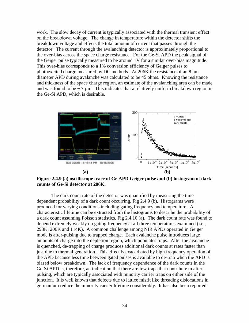
Time [seconds](a) (b)
work. The slow decay of current is typically associated with the thermal transient effect on the breakdown voltage. The change in temperature within the detector shifts the breakdown voltage and effects the total amount of current that passes through the detector. The current through the avalanching detector is approximately proportional to the over-bias across the space charge resistance. For the Ge-Si APD the peak signal of the Geiger pulse typically measured to be around 1V for a similar over-bias magnitude. This over-bias corresponds to a 1% conversion efficiency of Geiger pulses to photoexcited charge measured by DC methods. At 206K the resistance of an 8 um diameter APD during avalanche was calculated to be 45 ohms. Knowing the resistance and thickness of the space charge region, an estimate of the avalanching area can be made and was found to be ~ 7 µm. This indicates that a relatively uniform breakdown region in the Ge-Si APD, which is desirable. Figure 2.4.9 (a) oscilliscope trace of Ge APD Geiger pulse and (b) histogram of dark counts of Ge-Si detector at 206K.
The dark count rate of the detector was quantified by measuring the time dependent probability of a dark count occurring, Fig 2.4.9 (b). Histograms were produced for varying conditions including gating frequency and temperature. A characteristic lifetime can be extracted from the histograms to describe the probability of a dark count assuming Poisson statistics, Fig 2.4.10 (a). The dark count rate was found to depend extremely weakly on gating frequency at all three temperatures examined (i.e., 293K, 206K and 114K). A common challenge among NIR APDs operated in Geiger mode is after-pulsing due to trapped charge. Each avalanche pulse introduces large amounts of charge into the depletion region, which populates traps. After the avalanche is quenched, de-trapping of charge produces additional dark counts at rates faster than just due to thermal generation. This effect is exacerbated by high frequency operation of the APD because less time between gated pulses is available to de-trap when the APD is biased below breakdown. The lack of frequency dependence of the dark counts in the Ge-Si APD is, therefore, an indication that there are few traps that contribute to after-pulsing, which are typically associated with minority carrier traps on either side of the junction. It is well known that defects due to lattice misfit like threading dislocations in germanium reduce the minority carrier lifetime considerably. It has also been reported
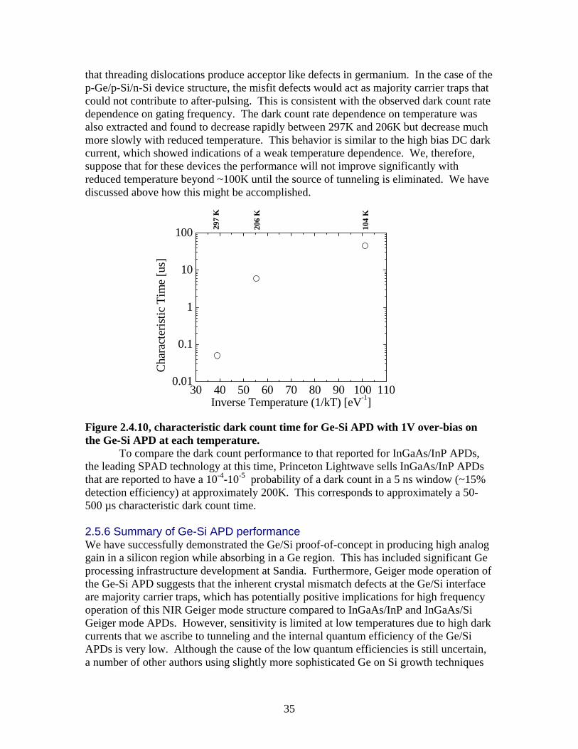
35
30 40 50 60 70 80 90 100 1100.01
0.1
1
10
100 206
K
104
K
297
K
Char
acte
ristic
Tim
e [u
s]
Inverse Temperature (1/kT) [eV-1]
that threading dislocations produce acceptor like defects in germanium. In the case of the p-Ge/p-Si/n-Si device structure, the misfit defects would act as majority carrier traps that could not contribute to after-pulsing. This is consistent with the observed dark count rate dependence on gating frequency. The dark count rate dependence on temperature was also extracted and found to decrease rapidly between 297K and 206K but decrease much more slowly with reduced temperature. This behavior is similar to the high bias DC dark current, which showed indications of a weak temperature dependence. We, therefore, suppose that for these devices the performance will not improve significantly with reduced temperature beyond ~100K until the source of tunneling is eliminated. We have discussed above how this might be accomplished. Figure 2.4.10, characteristic dark count time for Ge-Si APD with 1V over-bias on the Ge-Si APD at each temperature. To compare the dark count performance to that reported for InGaAs/InP APDs, the leading SPAD technology at this time, Princeton Lightwave sells InGaAs/InP APDs that are reported to have a 10-4-10-5 probability of a dark count in a 5 ns window (~15% detection efficiency) at approximately 200K. This corresponds to approximately a 50-500 µs characteristic dark count time. 2.5.6 Summary of Ge-Si APD performance We have successfully demonstrated the Ge/Si proof-of-concept in producing high analog gain in a silicon region while absorbing in a Ge region. This has included significant Ge processing infrastructure development at Sandia. Furthermore, Geiger mode operation of the Ge-Si APD suggests that the inherent crystal mismatch defects at the Ge/Si interface are majority carrier traps, which has potentially positive implications for high frequency operation of this NIR Geiger mode structure compared to InGaAs/InP and InGaAs/Si Geiger mode APDs. However, sensitivity is limited at low temperatures due to high dark currents that we ascribe to tunneling and the internal quantum efficiency of the Ge/Si APDs is very low. Although the cause of the low quantum efficiencies is still uncertain, a number of other authors using slightly more sophisticated Ge on Si growth techniques
36
have shown much higher quantum efficiencies and longer minority carrier lifetimes. We therefore conclude that the primary source of uncertainty in achieving the desired sensitivities originally sought at the beginning of the proposal is better control of the tunneling at reduced temperature (or Ge/Si interface defects). Nevertheless, even with the current tunneling effects, the dark count rates are approaching those reported for InGaAs/InP without the same after-pulsing penalties. 2.5.7 References [1] G. Masini, C. Lorenzo, F. Galluzzi, and G. Assanto, "Near-infrared
photodetectors based on polycrystalline Ge evaporated on Si<100> substrates," Philosophical Magazine B, vol. 80, pp. 791, 2000.
[2] P. R. Bandaru, S. Sahni, E. Yablonovitch, J. Liu, H.-J. Kim, and Y.-H. Xie, "Fabrication and characterization of low temperature (<450C) grown p-Ge/n-Si photodetectors for silicon based photonics," Material Science and Engineering B, vol. 113, pp. 79-84, 2004.
[3] L. Colace, G. Masini, G. Assanto, H.-C. Luan, K. Wada, and L. C. Kimerling, "Efficient high-speed near-infrared Ge photodetectors integrated on Si substrates," Applied Physics Letters, vol. 76, pp. 1231, 2000.
[4] O. Dosunmu, D. D. Cannon, M. K. Emsley, B. Ghyselen, J. Liu, L. C. Kimmerling, and M. S. Unlu, "Resonant Cavity Enhanced Ge Photodetectors for 1550 nm Operation on Reflecting Substrates," IEEE J. of Selected Topics in Quantum Electronics, vol. 10, pp. 694, 2004.
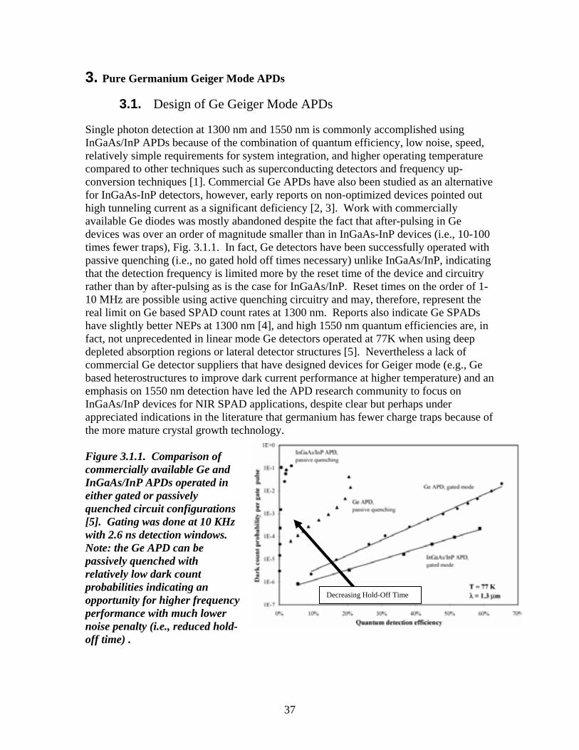
37
3. Pure Germanium Geiger Mode APDs
3.1. Design of Ge Geiger Mode APDs
Single photon detection at 1300 nm and 1550 nm is commonly accomplished using InGaAs/InP APDs because of the combination of quantum efficiency, low noise, speed, relatively simple requirements for system integration, and higher operating temperature compared to other techniques such as superconducting detectors and frequency up-conversion techniques [1]. Commercial Ge APDs have also been studied as an alternative for InGaAs-InP detectors, however, early reports on non-optimized devices pointed out high tunneling current as a significant deficiency [2, 3]. Work with commercially available Ge diodes was mostly abandoned despite the fact that after-pulsing in Ge devices was over an order of magnitude smaller than in InGaAs-InP devices (i.e., 10-100 times fewer traps), Fig. 3.1.1. In fact, Ge detectors have been successfully operated with passive quenching (i.e., no gated hold off times necessary) unlike InGaAs/InP, indicating that the detection frequency is limited more by the reset time of the device and circuitry rather than by after-pulsing as is the case for InGaAs/InP. Reset times on the order of 1-10 MHz are possible using active quenching circuitry and may, therefore, represent the real limit on Ge based SPAD count rates at 1300 nm. Reports also indicate Ge SPADs have slightly better NEPs at 1300 nm [4], and high 1550 nm quantum efficiencies are, in fact, not unprecedented in linear mode Ge detectors operated at 77K when using deep depleted absorption regions or lateral detector structures [5]. Nevertheless a lack of commercial Ge detector suppliers that have designed devices for Geiger mode (e.g., Ge based heterostructures to improve dark current performance at higher temperature) and an emphasis on 1550 nm detection have led the APD research community to focus on InGaAs/InP devices for NIR SPAD applications, despite clear but perhaps under appreciated indications in the literature that germanium has fewer charge traps because of the more mature crystal growth technology.
Figure 3.1.1. Comparison of commercially available Ge and InGaAs/InP APDs operated in either gated or passively quenched circuit configurations [5]. Gating was done at 10 KHz with 2.6 ns detection windows. Note: the Ge APD can be passively quenched with relatively low dark count probabilities indicating an opportunity for higher frequency performance with much lower noise penalty (i.e., reduced hold-off time) .
Decreasing Hold-Off Time

38
3.1.2. Approach After-pulsing is the primary challenge to operating InGaAs/InP detectors at
frequencies greater than 100 KHz. To significantly reduce charge traps, we are proposing to investigate SPAD devices and materials with lower charge trap densities like silicon or germanium. A critical challenge to improving the performance of commercially available germanium APDs is the reduction of dark counts from sources like tunneling unrelated to after-pulsing. Germanium APDs specifically designed for Geiger-mode rather than communications are expected to have better performance than the commercially available and predominantly literature reported cases. Doping profiles designed for greater breakdown fields (i.e., lower average fields and tunneling or higher breakdown) combined with device fabrication improvements like dopant in-diffusion (to avoid implant damage) and local metal gettering processes are expected to significantly improve dark count rates. Process changes like dopant in-diffusion and local metal gettering with heavy phosphorus diffusions were critical in reducing dark-counts in silicon Geiger-mode detectors in the 1990s from order of 1 MHz to 10 Hz at room temperature. Furthermore, the introduction of a wider band gap heterojunction with germanium like GaAs or GeSi could significantly improve the design space for Ge based APDs especially with respect to tunneling and higher temperature operation. Geiger-mode performance of GaAs APDs has shown some promise of performing nearly as well as silicon, therefore, we do not expect the same after-pulsing challenges with GaAs as which is observed with InP.
Work on pure germanium APDs was pursued because at the time of the initial desing work it was unclear how we would purchase Ge/GeSi and Ge/GaAs epitaxy. Designs of pure germanium APDs with guard rings, high breakdown voltages and relatively wide depletion regions were made. High breakdown voltages are desirable to limit tunneling at high bias. Masks for the new germanium APDs were purchased and a proposed process flow worked out to build the Ge devices in the MDL. To do this, 6” germanium substrates were purchased to evaluate both the material quality and the compatibility of the material with standard MDL processing.
3.1.3. References [1] P. Kumar, et al. Quantum Information Processing , vol. 3, pp. 215, 2004. [2] A. L. Lacaita, et al. Applied Optics , vol. 33, pp. 6902, 1994. [3] G. Ribordy et al. Applied Optics , vol. 37, pp. 2272, 1998. [4] P. A. Hiskett et al. Applied Optics , vol. 39, pp. 6818, 2000. [5] D. P. Mathur et al. Applied Optics , vol. 9, pp. 1842, 1970.
39
3.2. Fabrication of Ion Implanted Ge APDs
3.2.1 Device fabrication (diffusion after Implantation) Renewed interest in the development of germanium based devices for advanced
CMOS, optoelectronic and radiation detection applications [1-3] has motivated recent studies to better characterize dopant implantation, activation and diffusion in germanium [4-6], which are critical process steps for the Ge APDs designed in this work. An accurate measurements of process parameters like diffusivity are necessary for numeric simulation of device fabrication and electrical performance. Phosphorus diffusion is of particular interest because of its high extrinsic diffusivity and its apparent limited solid solubility of ~ 2-3x1019 cm-3, which presents a challenge to controlled n+ junction formation. Most recent published work on phosphorus diffusion has focused on short anneals after the implant [4-6]. It is not well established what contribution to the dopant diffusivity in germanium can be produced by non-equilibrium effects like radiation damage (e.g., transient enhanced diffusion), surface effects (e.g., segregation) or anneal ambient (e.g., oxidation enhanced diffusion) that have been studied extensively in silicon. For example, a common assertion is that most dopants diffuse in germanium via vacancy mediated mechanisms, which has potential implications for the anticipated strength of transient enhanced diffusion effects. Transient enhanced diffusion effects are observed strongly in self-interstitial mediated diffusers like boron or phosphorus (in silicon) but less strongly for vacancy diffusers like antimony (in silicon), which suggests that transient enhanced diffusion effects might be relatively weak for dopants in germanium. In this work, we show that previously reported phosphorus diffusivities calculated from profiles produced after rapid thermal annealing (RTA) do not accurately predict diffusion profiles after hours of annealing at similar temperatures as the RTAs. This suggests a non-negligible transient enhanced diffusion in germanium for phosphorus. The average phosphorus diffusivities measured during the long anneals in this work are presented and an extrinsic activation energy of 2.3 eV is measured over the temperature range of 600-800˚C. Furthermore, the experimentally obtained profiles were best fit numerically through use of both a temperature dependent segregation term between the germanium and capping oxide as well as a peak solid solubility well below the peak implant concentration.
3.2.1 Experiment & discussion A gallium doped (>10 ohm-cm), (100) orientation, 150 mm, UMICORE germanium substrate was capped with a 25 nm thick oxide followed by a 25 nm thick nitride. The oxide and nitride were deposited by high density plasma chemical vapor deposition. The germanium was then implanted with a 160 keV, 4x1015 cm-2 phosphorus implant using a 7 degree tilt and 22 degree rotation.

40
Figure 3.2.1. Phosphorus profiles in germanium before and after annealing measured by secondary ion mass spectrometry (SIMS) overlaid on spreading resistance profiles (SRP). N2/H2 indicates forming gas and N2 indicates nitrogen anneal only. After implant the wafer was cleaved into smaller samples some of which were annealed at temperatures of 600˚C, 700˚C or 800˚C for either 3 or 10 hours in forming gas (20% H2 in N2) or nitrogen ambients. Furnace temperatures were monitored with calibrated K-type thermocouples that have an accuracy of ±0.2°C. Chemical doping and carrier concentration profiles were obtained by secondary ion mass spectrometry (SIMS) or spreading resistance probe (SRP), respectively, Fig. 3.2.1.The SIMS measurements were done using sputtering conditions, which have previously been found to reproduce integrated doses in close agreement with Rutherford backscattering (RBS) [6]. Carrier concentrations were calculated from spreading resistance profiles that used calibration standards from the analysis laboratory Solecon Laboratories, which assumes that mobilities are similar to those used in their standards (i.e., similar to commonly reported single crystal mobilities). Good agreement between SRP and SIMS background doping was found and for shallow SIMS profiles the concentrations agreed up to approximately 1019 cm-3. For deep profiles (i.e., after 3 hour annealing at 800C) SIMS shows an extended profile compared to SRP, which SIMS indicates approximately a factor of 2 greater phosphorus concentrations near the surface. Extended profiles in SIMS due to “knock-on” or sputtered segregation effects are observed under certain conditions and are exaggerated for deep profiling, which is consistent with this work. Disagreement between SRP and SIMS at high concentrations has also been discussed elsewhere [4-6]and is believed to be a disagreement in calibration. Because the SIMS calibration used in this work is known to agree within 20% with RBS [6], we rely on the SIMS profiles to model the diffusivity and dose loss in this work. .
0 1 2 3 4 5 6 71014
1015
1016
1017
1018
1019
1020
1021
Con
cent
ratio
n [c
m-3]
Depth [µm]
800oC, 3 hours, N2/H2 (SIMS) As-implanted (SIMS) 600oC, 3 hours, N2/H2 (SIMS) 700oC, 3 hours, N2/H2 (SIMS) 600oC, 3 hours, N2/H2 (SRP) 700oC, 3 hours, N2/H2 (SRP) 800oC, 3 hours, N2/H2 (SRP) 700oC, 3 hours, N2 (SIMS) 700oC, 10 hours, N2/H2 (SIMS)

41
0 1 2 3 4 5 6 7 8 9 101015
1016
1017
1018
1019
1020
1021
Phos
phor
us C
once
ntra
tion
[cm
-3]
Depth [um]
As-implanted (SIMS) 600oC, 3 hours, N2/H2 (SIMS) 700oC, 3 hours, N2/H2 (SIMS) 800oC, 3 hours, N2/H2 (SIMS) 600oC, 3 hours, N2/H2 (fit) 700oC, 3 hours, N2/H2 (fit) 800oC, 3 hours, N2/H2 (fit) 600oC, 3 hours, N2/H2 (Chui et al.) 700oC, 3 hours, N2/H2 (Chui et al.) 800oC, 3 hours, N2/H2 (Chui et al.)
Figure 3.2.2. Phosphorus profiles in germanium before and after annealing (circles, squares, and triangles) measured by secondary ion mass spectrometry (SIMS) overlaid on simulated profiles using diffusivities measured in this work (solid, dashed, and dotted lines). Simulated profiles using previously reported diffusivities by Chui et al. are also shown (+, -, and x symbols)
Profiles were also numerically calculated using the published implant data and diffusivities [4] and were found to agree relatively well with the published SRP data showing that the disagreement is not related to the simulation package or model itself. Profiles obtained with SIMS were compared to numerically simulated profiles [TSUPREM4] using recently published phosphorus diffusivities [4]. The profiles measured with SIMS are considerably shallower than that predicted by the recent literature values, Fig. 3.2.2. In this work, no appreciable difference in profiles was observed between samples annealed in nitrogen or forming gas, therefore, the disagreement is not believed to be due to an effect of different ambients. That is, although there are previous reports of hydrogen affecting the vacancy concentration in germanium [7], no appreciable change in diffusivity is observed due to the presence of the hydrogen in the forming gas anneals
To obtain the average phosphorus diffusivities for these relatively long thermal budgets, each profile was simulated varying the phosphorus diffusivity until the best fit was achieved, Fig. 3.2.2. Care was taken to incorporate the effects of the germanium bandgap (e.g., intrinsic carrier concentration) and a peak solid solubility of 2x1019 cm-3 was used for all temperatures, which is observed in SRP measurements of high dose phosphorus implants previously [8]. It has also been recently observed that some of the phosphorus dose is lost to diffusion out of the surface [5]. The mechanism by which the phosphorus is lost is not well understood and appears to occur both with and without oxide capping layers. The dose loss was modeled for this case with a segregation model that predicts a flux across the interface proportional to an interface transport coefficient and the difference of the equilibrium concentrations determined by a segregation coefficient between the capping oxide and the underlying germanium. The transport
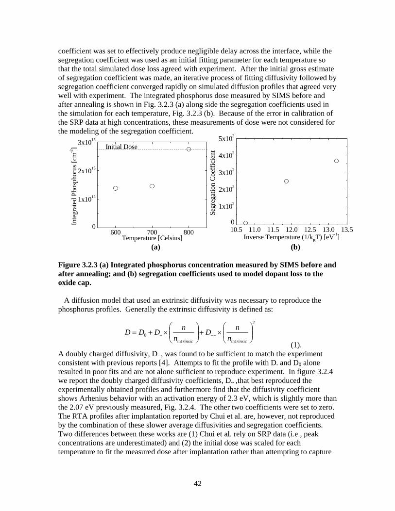
42
2
intint0 ⎟⎟
⎠
⎞⎜⎜⎝
⎛×+⎟⎟
⎠
⎞⎜⎜⎝
⎛×+= −−−
rinsicrinsic nnD
nnDDD
10.5 11.0 11.5 12.0 12.5 13.0 13.50
1x10²
2x10²
3x10²
4x10²
5x10²
Segr
egat
ion
Coef
ficie
nt
Inverse Temperature (1/kBT) [eV-1]600 700 800
0
1x10¹⁵
2x10¹⁵
3x10¹⁵
Inte
grat
ed P
hosp
horu
s [cm
-2]
Temperature [Celsius]
Initial Dose
coefficient was set to effectively produce negligible delay across the interface, while the segregation coefficient was used as an initial fitting parameter for each temperature so that the total simulated dose loss agreed with experiment. After the initial gross estimate of segregation coefficient was made, an iterative process of fitting diffusivity followed by segregation coefficient converged rapidly on simulated diffusion profiles that agreed very well with experiment. The integrated phosphorus dose measured by SIMS before and after annealing is shown in Fig. 3.2.3 (a) along side the segregation coefficients used in the simulation for each temperature, Fig. 3.2.3 (b). Because of the error in calibration of the SRP data at high concentrations, these measurements of dose were not considered for the modeling of the segregation coefficient.
(a) (b)
Figure 3.2.3 (a) Integrated phosphorus concentration measured by SIMS before and after annealing; and (b) segregation coefficients used to model dopant loss to the oxide cap.
A diffusion model that used an extrinsic diffusivity was necessary to reproduce the phosphorus profiles. Generally the extrinsic diffusivity is defined as:
(1). A doubly charged diffusivity, D--, was found to be sufficient to match the experiment consistent with previous reports [4]. Attempts to fit the profile with D- and D0 alone resulted in poor fits and are not alone sufficient to reproduce experiment. In figure 3.2.4 we report the doubly charged diffusivity coefficients, D-- ,that best reproduced the experimentally obtained profiles and furthermore find that the diffusivity coefficient shows Arhenius behavior with an activation energy of 2.3 eV, which is slightly more than the 2.07 eV previously measured, Fig. 3.2.4. The other two coefficients were set to zero. The RTA profiles after implantation reported by Chui et al. are, however, not reproduced by the combination of these slower average diffusivities and segregation coefficients. Two differences between these works are (1) Chui et al. rely on SRP data (i.e., peak concentrations are underestimated) and (2) the initial dose was scaled for each temperature to fit the measured dose after implantation rather than attempting to capture
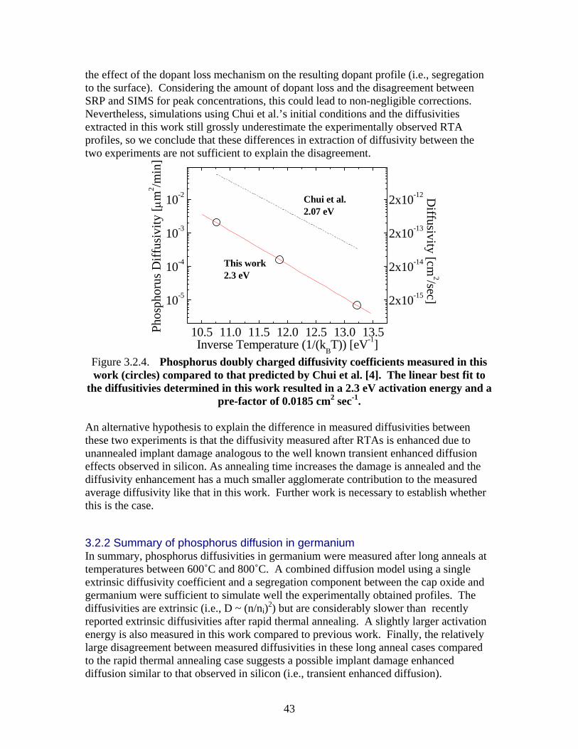
43
10.5 11.0 11.5 12.0 12.5 13.0 13.5
10-5
10-4
10-3
10-2
2x10-15
2x10-14
2x10-13
2x10-12Chui et al.2.07 eV
This work2.3 eV
Diffusivity [cm
2/sec]
Phos
phor
us D
iffus
ivity
[µm
2 /min
]
Inverse Temperature (1/(kBT)) [eV-1]
the effect of the dopant loss mechanism on the resulting dopant profile (i.e., segregation to the surface). Considering the amount of dopant loss and the disagreement between SRP and SIMS for peak concentrations, this could lead to non-negligible corrections. Nevertheless, simulations using Chui et al.’s initial conditions and the diffusivities extracted in this work still grossly underestimate the experimentally observed RTA profiles, so we conclude that these differences in extraction of diffusivity between the two experiments are not sufficient to explain the disagreement.
Figure 3.2.4. Phosphorus doubly charged diffusivity coefficients measured in this work (circles) compared to that predicted by Chui et al. [4]. The linear best fit to
the diffusitivies determined in this work resulted in a 2.3 eV activation energy and a pre-factor of 0.0185 cm2 sec-1.
An alternative hypothesis to explain the difference in measured diffusivities between these two experiments is that the diffusivity measured after RTAs is enhanced due to unannealed implant damage analogous to the well known transient enhanced diffusion effects observed in silicon. As annealing time increases the damage is annealed and the diffusivity enhancement has a much smaller agglomerate contribution to the measured average diffusivity like that in this work. Further work is necessary to establish whether this is the case.
3.2.2 Summary of phosphorus diffusion in germanium In summary, phosphorus diffusivities in germanium were measured after long anneals at temperatures between 600˚C and 800˚C. A combined diffusion model using a single extrinsic diffusivity coefficient and a segregation component between the cap oxide and germanium were sufficient to simulate well the experimentally obtained profiles. The diffusivities are extrinsic (i.e., D ~ (n/ni)2) but are considerably slower than recently reported extrinsic diffusivities after rapid thermal annealing. A slightly larger activation energy is also measured in this work compared to previous work. Finally, the relatively large disagreement between measured diffusivities in these long anneal cases compared to the rapid thermal annealing case suggests a possible implant damage enhanced diffusion similar to that observed in silicon (i.e., transient enhanced diffusion).

44
3.2.3 References [1] C. O. Chui, H. Kim, D. Chi, B. Triplett, P. McIntyre, and K. Saraswat, “A sub-400C Germanium MOSFET Technology with High-k Dielectric and Metal Gate,” presented at IEDM, Washington, D. C., 2002. [2] R. E. Jones, S. G. Thomas, S. Bharatan, R. Thoma, C. Jasper, T. Zirkle, N. V. Edwards, R. Liu, X. D. Wang, Q. Xie, C. Rosenblad, J. Ramm, G. Isella, H. Kanel, J. Oh, and J. C. Campbell, “Fabrication and Modelling of Gigahertz Photodetectors in Heteroepitaxial Ge-on-Si Using a Graded Buffer Layer Deposited by Low Energy PLasma Enhanced CVD,” presented at IEDM, 2002. [3] O. I. Dosunmu, D. D. Cannon, M. K. Emsley, B. Ghyselen, J. Liu, L. C. Kimerling, and M. S. Unlu, “Resonant Cavity Enhanced Ge Photodetectors for 1550 nm Operation on Reflecting Si Substrates,” IEEE J. of Selected Topics in Quantum Electronics, vol. 10, pp. 694, 2004. [4] C. O. Chui, K. Gopalakrishnan, P. Griffin, J. D. Plummer, and K. C. Saraswat, “Activation and diffusion studies of ion-implanted p and n dopants in germanium,” Applied Physics Letters, vol. 83, pp. 3275, 2003. [5] C. H. Poon, L. S. Tan, B. J. Cho, and A. Y. Du, “Dopant Loss Mechanism in n+/p Germanium Junctions during Rapid Thermal Annealing,” Journal of the Electrochemical Society, vol. 152, pp. G895, 2005.
3.3. Germanium APD Device Fabrication
Initial concerns about chemical and structural compatibility with the MDL silicon CMOS line have been subsequently addressed. Tests were carried out that showed germanium to be relatively benign for the silicon CMOS process flow because germanium is relatively easy to etch and therefore clean up. To insure that germanium devices are not destroyed by the standard silicon processes, because of the facility in etching germanium, the process flow was also designed to completely entomb the germanium substrate within an oxide-nitride barrier layers that will only be opened late in the process to make contact to the substrate. This has worked only partially because scratches and pin-hole defects do expose the underlying surface to considerable micro-etching. Structurally, substrates were also tested for compatibility with MDL tools (e.g., robot handlers) and found that the germanium substrates are compatible. However, because the germanium substrates are softer and warp more than silicon substrates under the same stresses induced by layer deposition on the wafers, radius of curvature (ROC) vs. dielectric thickness experiments were required to insure that the minimum dielectric thicknesses for the MDL metallization process could be deposited while still being able to satisfy the ROC requirements of the MDL lithography tools.
Maintaining a long minority carrier lifetime in the germanium is a key to reaping the anticipated advantage of this material (i.e., low dark currents and charge traps). To measure this property directly in our detector materials, a lifetime measurement set-up was also built in the MDL, which can measure lifetimes from milliseconds to nanoseconds in common bulk semiconductors. Lifetimes in germanium substrates were measured and found to be greater than ~ 0.5x10⁻³ seconds, which is 5 times greater than what was used for the germanium device simulations. If these lifetimes can be sustained

45
0 1000 2000 3000 4000 50000
200
400
600
800
1000
1200
1400
Rad
ius o
f Cur
vatu
re [m
]
PECVD Oxide Thickness [ A ]
Germanium Silicon
(a) (b)
through the device processing then simulated dark currents in the germanium devices represent a conservative estimate. Figure 3.3.1 (a) radius of curvature dependence on stress for Ge and Si substrates and (b) unintentional etch pits formed at trench edges and through pin holes in the thin oxide/nitride/oxide stack. Germanium is a softer material with a lower yield strength than silicon leading to larger radii of curvature for the same dielectric thickness. High radii of curvature cause problems for lithography and plastic deformation produces detrimental defects. The fabrication of the germanium APDs used similar processing techniques as planar silicon diodes. However, the processing of 6” germanium wafers did require some special processing considerations. One challenge in processing germanium is that germanium oxide dissolves in water making it extremely easy to etch in most wet chemistries used to process silicon. To protect the germanium substrates from the wet processing, a dielectric stack was deposited on both the front and backsides. It was found, however, that when thick dielectrics were deposited on the germanium under certain high stress conditions slip dislocations would form and sometimes the wafer would plastically deform. To avoid stressing the wafers beyond their yield strength, the dielectric thicknesses were limited to under 300 nm on both sides. A consequence of this was that the thinner dielectrics did not always provide sufficient coverage, for example over trenched alignment marks and through pin-holes, to completely avoid etching of the surface. The desire to avoid wet chemistries also led to process flows without CMP. CMP is a wet chemistry intensive technique and it was unclear that there was sufficient time to develop this process for the Ge APD flow. The consequence of not using CMP was that topography during the metalization step led to shorts from stringers. A careful tuning was required to etch stringer metal without completely removing the passivating top oxide/nitride/oxide stack. Finally, it was also found that high doses of phosphorus that produced concentrations well above the solid-solubility produce crater defects when annealing temperatures were above 400°C.

46
3.4. Ge APD Device Performance
The final Ge vertical structure consisted of a phosphorus implant into a high resistivity p-type 100 substrate. Circular devices with n-type implant regions of diameters from 8 – 500 um were fabricated and varying guard ring sizes were used. A lighter n-type guard ring implant was used. Both n and p contacts were made using a Ti/Ti-nitride/aluminum deposition over 0.7 um x 0.7 um windows etched in the oxide above the contact regions. The nominal dielectric thickness was 0.3 um. The Al ring width on the top surface of the n-type contact was approximately 2 µm around the outer edge of the detector.
Room temperature and reduced temperature I-V measurements were made to characterize the dark current performance and optical response, Fig. 3.4.1 (a) & (b). The current response of the Ge device shows good rectification and a relatively flat leakage current dependence at high biases, between 3-20V, up to the commencement of multiplication gain in the junction at around 15 V. The measured room temperature dark currents are within an order of magnitude of typical specifications for commercial detectors and differences may be primarily due to the choice of surface passivation.
Figure 3.4.1 Dark current dependence of Ge APDs on temperature The photoresponse of the germanium detectors was subsequently examined using 1310 nm light at a series of different temperatures. 1310 nm light was selected to avoid complications related to the shift of the bandgap with temperature, which effects 1550 responsivity. A future study will look at the sensitivity of these devices at 1550 nm at reduced temperature. A relatively flat photoresponse is observed at all temperatures up to approximately 15V at which point evidence of photomultiplication is observed. The responsivity of the detector at room temperature is measured to be ~ 0.2 A/W without an
0 10 20 3010-10
10-9
10-8
10-7
10-6
10-5
55K 65K 21K 297K 250K 164K
Cur
rent
[A]
Applied Bias [V]

47
0 10 20 3010-10
10-9
10-8
10-7
10-6
10-5
10-4
T=297 photo (T=297) photo (T=164) T=164 T=250 photo (T=250)
Curre
nt [A
]
Applied Bias [V]0 5 10 15 20 25 30 3510-1
100
101
102
103
T=21K T=297K T=250K T=164K
Mul
tiplic
atio
n
Applied Bias [V](a) (b)
AR coating. Considering that little effort was made to optimize the surface passivation, this result is relatively close to commercial performance. The multiplication gain calculated in Fig 3.4.2 (b) as: multiplication = (I – Idark )/I1V. Gains between 2 to 100 can be observed from the I-Vs although the maximum gains are underestimated because the photocurrent saturates at the current compliance before the dark current. Further work is needed to better understand the dark current dependence on temperature, however, from Fig 3.4.1 that continued reduction of temperature leads to a reduction in dark current rather than being pinned because of tunneling. This is promising for operation in Geiger mode, for which commercial APDs are reported to typically be limited because of tunneling current. Ideally, higher breakdown voltages are desirable to minimize the electric field at avalanche breakdown and avoid tunneling contributions. These I-Vs are for the smallest diameter n implants, which produces the lowest breakdowns. Future work will move to examine the larger n-type implant devices, which have much higher breakdown voltages. The breakdown voltage of the smaller device is due to lateral depletion effects.
Figure 3.4.2 (a) Temperature dependence of the photoresponse of Ge APDs and (b) the Ge APD gain dependence on temperature. Note that the gain is underestimated because of current compliance limit set on the measurements from (a) used to calculate the gain in (b). Geiger mode testing of these devices has just begun. The devices do operate in Geiger mode and are sensitive to small numbers of photons determined through gross estimates of gated operation under attenuated CW operation. However, further work is required to determine the exact detection efficiencies and dark count rates of these devices. Funding for an IC-post-doc has been acquired to further examine Ge detectors in Geiger mode. 4. InGaAs Based Avalanche Photodiodes
4.1. InGaAs/InAlAs APDs
4.1.1 InGaAs/InAlAs APD Device Design and Fabrication The well established APD technology with sensitivity at a wavelength of 1550 nm is the InGaAs/InP APD that was introduced in 1982 [1] and subsequently commercialized for
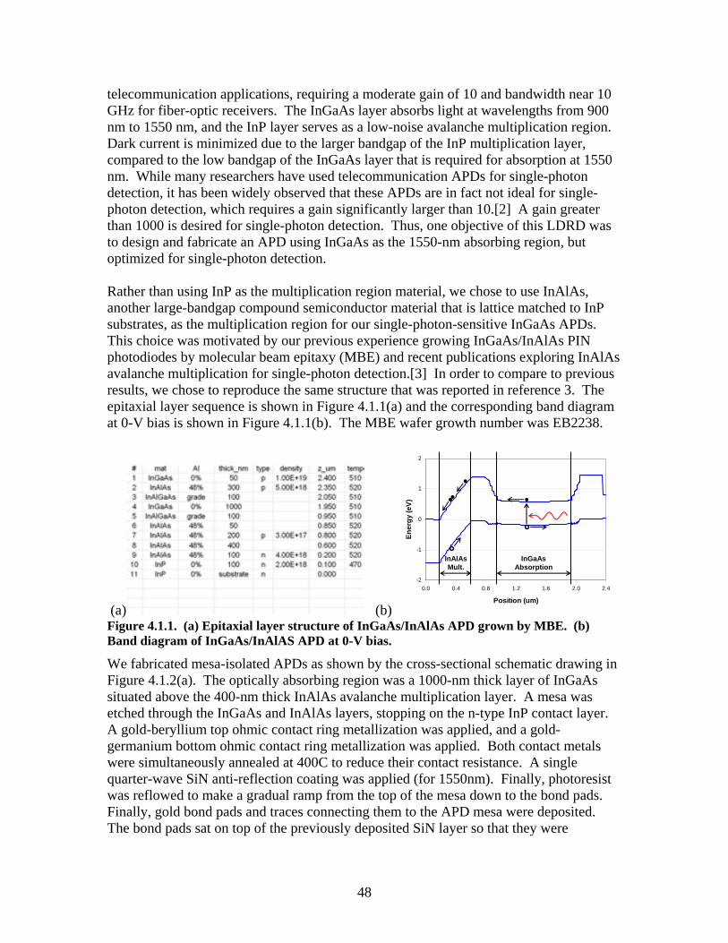
48
telecommunication applications, requiring a moderate gain of 10 and bandwidth near 10 GHz for fiber-optic receivers. The InGaAs layer absorbs light at wavelengths from 900 nm to 1550 nm, and the InP layer serves as a low-noise avalanche multiplication region. Dark current is minimized due to the larger bandgap of the InP multiplication layer, compared to the low bandgap of the InGaAs layer that is required for absorption at 1550 nm. While many researchers have used telecommunication APDs for single-photon detection, it has been widely observed that these APDs are in fact not ideal for single-photon detection, which requires a gain significantly larger than 10.[2] A gain greater than 1000 is desired for single-photon detection. Thus, one objective of this LDRD was to design and fabricate an APD using InGaAs as the 1550-nm absorbing region, but optimized for single-photon detection. Rather than using InP as the multiplication region material, we chose to use InAlAs, another large-bandgap compound semiconductor material that is lattice matched to InP substrates, as the multiplication region for our single-photon-sensitive InGaAs APDs. This choice was motivated by our previous experience growing InGaAs/InAlAs PIN photodiodes by molecular beam epitaxy (MBE) and recent publications exploring InAlAs avalanche multiplication for single-photon detection.[3] In order to compare to previous results, we chose to reproduce the same structure that was reported in reference 3. The epitaxial layer sequence is shown in Figure 4.1.1(a) and the corresponding band diagram at 0-V bias is shown in Figure 4.1.1(b). The MBE wafer growth number was EB2238.
(a) (b)
-2
-1
0
1
2
0.0 0.4 0.8 1.2 1.6 2.0 2.4
Position (um)
Ener
gy (e
V)
InAlAsMult.
InGaAsAbsorption
-2
-1
0
1
2
0.0 0.4 0.8 1.2 1.6 2.0 2.4
Position (um)
Ener
gy (e
V)
InAlAsMult.
InGaAsAbsorption
Figure 4.1.1. (a) Epitaxial layer structure of InGaAs/InAlAs APD grown by MBE. (b) Band diagram of InGaAs/InAlAS APD at 0-V bias.
We fabricated mesa-isolated APDs as shown by the cross-sectional schematic drawing in Figure 4.1.2(a). The optically absorbing region was a 1000-nm thick layer of InGaAs situated above the 400-nm thick InAlAs avalanche multiplication layer. A mesa was etched through the InGaAs and InAlAs layers, stopping on the n-type InP contact layer. A gold-beryllium top ohmic contact ring metallization was applied, and a gold-germanium bottom ohmic contact ring metallization was applied. Both contact metals were simultaneously annealed at 400C to reduce their contact resistance. A single quarter-wave SiN anti-reflection coating was applied (for 1550nm). Finally, photoresist was reflowed to make a gradual ramp from the top of the mesa down to the bond pads. Finally, gold bond pads and traces connecting them to the APD mesa were deposited. The bond pads sat on top of the previously deposited SiN layer so that they were

49
electrically isolated from the substrate. An optical photograph of the resulting device is shown in Figure 4.1.2(b).
(a)
n-InP
p-InAlAsi-InGaAs
i-InAlAs
Absorption
Multiplication
n-InP
p-InAlAsi-InGaAs
i-InAlAs
Absorption
Multiplication
(b) Figure 4.1.2. (a) Cross sectional schematic of InGaAs/InAlAs APD device. (b) Top view optical micrograph of fabricated InGaAs/InAlAs APD device.
4.1.2 InGaAs/InAlAs APD Device Characterization Room temperature (300K) current-voltage (IV) characteristics of the APD are shown in Figure 4.1.3(a). The blue trace shows the dark current obtained with no optical illumination. The red curve shows the photocurrent obtained with optical illumination, although the exact power level of the incident optical illumination was not calibrated in this measurement. The most important feature to observe is that avalanche breakdown occurs at a voltage of 34.0 V, with or without optical illumination. The second most important feature to note is that very little photocurrent is obtained below the so-called punch-through voltage of 25.4 V. The importance of punch-through for separate absorption and multiplication (SAM) APDs is illustrated by the band diagram simulations shown in Figure 4.1.3(b).* The blue curves in Figure 4.1.3(b) show the conduction and valence bands at a bias voltage below punch-through, where the lack of a significant electric field (blue curve slope) in the InGaAs absorption layer prevents electrons from being transported to the InAlAs multiplication layer. As the bias voltage is increased above punch-through, we obtain the bands shown in red in Figure 4.1.3(b). Above punch-through, an electric field exists in the InGaAs absorption layer that causes photo-generated electrons to drift to the InAlAs layer where they experience avalanche multiplication, creating additional electron-hole pairs. In a well-engineered SAM APD, the doping levels are such that punch-through is achieved at a voltage below the avalanche breakdown voltage. At the same time, punch-through should not occur too far below the avalanche breakdown voltage, because in this case, by the time the voltage has been increased to obtain high avalanche gain, the electric field in the InGaAs region will be so large that excessive dark current results from band-to-band tunneling in the InGaAs layer. Just above the punch-through voltage in Figure 4.1.3(a), the avalanche gain is * SimWindows version 1.5 was used to simulate the InGaAs APD device. However, because SimWindows provides only a 1-D simulation, the predicted punch-through voltage differs from the measured value. Also, there may be some errors in our assumptions about some material properties used in SimWindows.

50
assumed to be G=1, since the voltage is still well below the avalanche breakdown voltage. As the bias voltage is increased toward the avalanche breakdown voltage, we observed that the multiplied photocurrent (red curve in Figure 4.1.3(a)) increases significantly above the G=1 level, due to the process of avalanche multiplication.
(a)
1.E-12
1.E-11
1.E-10
1.E-09
1.E-08
1.E-07
1.E-06
1.E-05
0 10 20 30 40
Reverse Bias (V)
Cur
rent
(A)
Dark Photo
Breakdown Punch
Through
G=1
G=10
L88K_EB2238B
T=300K
(b)
-60
-50
-40
-30
-20
-10
0
10
0.0 0.4 0.8 1.2 1.6 2.0 2.4
Position (um)
Ener
gy (e
V)
InAlAsMult.
InGaAsAbsorption
50V
40V
-60
-50
-40
-30
-20
-10
0
10
0.0 0.4 0.8 1.2 1.6 2.0 2.4
Position (um)
Ener
gy (e
V)
InAlAsMult.
InGaAsAbsorption
50V
40V
Figure 4.1.3. (a) Room-temperature IV characteristics of InGaAs/InAlAs APD with (red) and without (blue) optical illumination. (b) Band diagram below (blue) and above (red) the punch-through voltage.
In order to measure the InGaAs/InAlAs APD properties at low temperatures, it was mounted on a header that could be mounted inside a closed-cycle helium-cooled cryostat, achieving temperatures from 300K down to 15K. Photographs of the APD device chip mounted on a header are shown in Figure 4.1.4(a). An electrically insulating shim of aluminum nitride was placed under the APD device chip in order to isolate the cathode, which is electrically connected to the n-type InP substrate, from the header. The header was mounted on a copper cold finger in the helium cryostat, as shown in Figure 4.1.4(b).
(a) (b) Figure 4.1.4. (a) InGaAs/InAlAs APD mounted on header, on electrically insulating AlN shim. (b) APD mounted on copper cold finger inside the helium cryostat.
The APD was illuminated through optically transparent windows on the cryostat, as shown in Figure 4.1.5(a). One of two fiber coupled laser diodes (one 1310-nm laser and one 1550-nm laser) was used as the illumination source. The laser diode was biased with

51
a DC current source and was optionally driven with a capacitively coupled electrical pulse for producing optical pulses. The laser output was passed through a fiber attenuator, having calibrated optical attenuation factors programmable from 0 to 60 dB. After the attenuator, the fiber output was collimated with an f=11-mm lens and then focused with an f=100-mm lens, yielding a focused beam of diameter of 2w0 = 86microns (where w0 is the radius at 1/e2 intensity) at the APD surface. The fraction of the incident optical power that fell within the diameter of our 50 and 70-micron aperture APDs was 49.1% and 73.4%, respectively. The DC bias of the laser diode was typically set so that the optical power immediately before the cryostat window was 1.0mW, with the fiber attenuator set at 0dB. With the cryostat window removed, we measured photocurrent from our 70-micron-aperture InGaAs APD versus incident power at 1550nm as shown in Figure 4.1.5(b), with VR=26V (G=1) and T=293K. The data show a responsivity of 0.69A/W, which corresponds to a quantum efficiency of 55% (very close to the expected 63% absorption for a 1000-nm thick InGaAs layer at 1550nm).
(a) (b)
1.E-08
1.E-07
1.E-06
1.E-05
1.E-08 1.E-07 1.E-06 1.E-05 1.E-04
Pin (W)
Iout
(A)
Figure 4.1.5. (a) Fiber-coupled illumination of APD inside cryostat at either 1310 or 1550nm. (b) Photocurrent versus incident optical power at 1550nm, for a 70-micron-aperture InGaAs APD biased at G=1 at room temperature.
In order to reduce dark counts, single-photon APDs are generally operated colder than room temperature. When the operating temperature of the InGaAs APD was decreased, the dark current decreased, the breakdown voltage decreased, and the punch-through voltage increased. These trends are apparent from the current-versus-voltage (IV) curves shown in Figure 4.1.6(a) and (b), obtained at 293K and 180K, respectively. The blue curves (dark) were obtained with no incident illumination. The pink (30dB) and red (20dB) curves were obtained with fiber attenuator settings of 30 and 20 dB, respectively, corresponding to 1uW and 10uW of 1550-nm optical power incident on the cryostat window. We note that the cryostat window transmission was measured to be 89% at 1550nm. The breakdown voltage, measured at a dark current of 0.1uA, was 34.5V at 293K and 30.6V at 180K. The punch-through voltage, measured with 1uW of 1550-nm light incident on the cryostat, was 22.6V at 293K and 25.6V at 180K. Because the bandgap of InGaAs increases as the temperature is lowered, the absorption at 1550nm will decrease as the APD is cooled and will drop abruptly below approximately 150K. At a bias of 26V (G=1), we measured the responsivity at 180K to be 93.2% of the 293K value. Thus, the quantum efficiency at 180K was still rather high (51%), indicating that the bandgap was still smaller than the 1550nm photon energy (0.80eV).

52
(a) (b) Figure 4.1.6. Current versus voltage data from a 50-micron-aperture InGaAs APD at temperatures of (a) 293K and (b) 180K. The blue curves show the dark current, and the pink and red curves show photocurrent obtained with 1uW and 10uW, respectively, of 1550-nm optical power incident on the cryostat window.
Most of the characterization of our InGaAs/InAlAs APDs was done without incident optical illumination. We typically ran the APD in Geiger mode, bringing the bias voltage approximately 0.5V above the breakdown voltage during a short (1-us long) gate pulse, delivered at a typical rate of 10kHz (every 100us). Because the APD was biased above breakdown during the gate pulse, a single optically or thermally generated carrier could initiate avalanche breakdown and create a significant current (typically about 0.2mA). Figures 4.1.7(a) and (b) show dark (thermally initiated) Geiger pulses from the APD for over-bias levels of 0.4 and 0.5V, respectively. Also, for example, Figure 4.1.7(b) shows that the avalanche current is quenched when the bias voltage is returned to a level 0.5V below the breakdown voltage, at the end of the gate pulse. Although we took much more data than we will discuss in this report, the most important conclusion is that our standard mesa-type photodiode device structure (described above) does not achieve the electric-field uniformity versus lateral position that we would desire from a SPAD. The consequence of poor uniformity is that the point of highest electric field is likely to breakdown due to a thermally generated carrier (dark event) before a photon absorbed in a region of lower electric field initiates breakdown (single-photon detection). Any future work on InGaAs APDs should address the field uniformity issue, by (for example) incorporating a guard ring. However, we also note that if the goal is to produce single-photon imaging focal plane arrays, with relatively small pixels (<20um), then the field uniformity issue may be improved inherently by the small-pixel-array geometry that is chosen.
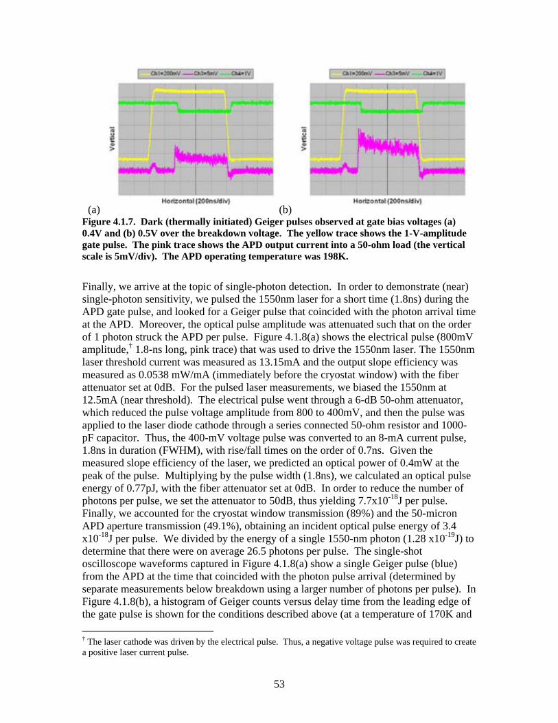
53
(a) (b) Figure 4.1.7. Dark (thermally initiated) Geiger pulses observed at gate bias voltages (a) 0.4V and (b) 0.5V over the breakdown voltage. The yellow trace shows the 1-V-amplitude gate pulse. The pink trace shows the APD output current into a 50-ohm load (the vertical scale is 5mV/div). The APD operating temperature was 198K.
Finally, we arrive at the topic of single-photon detection. In order to demonstrate (near) single-photon sensitivity, we pulsed the 1550nm laser for a short time (1.8ns) during the APD gate pulse, and looked for a Geiger pulse that coincided with the photon arrival time at the APD. Moreover, the optical pulse amplitude was attenuated such that on the order of 1 photon struck the APD per pulse. Figure 4.1.8(a) shows the electrical pulse (800mV amplitude,† 1.8-ns long, pink trace) that was used to drive the 1550nm laser. The 1550nm laser threshold current was measured as 13.15mA and the output slope efficiency was measured as 0.0538 mW/mA (immediately before the cryostat window) with the fiber attenuator set at 0dB. For the pulsed laser measurements, we biased the 1550nm at 12.5mA (near threshold). The electrical pulse went through a 6-dB 50-ohm attenuator, which reduced the pulse voltage amplitude from 800 to 400mV, and then the pulse was applied to the laser diode cathode through a series connected 50-ohm resistor and 1000-pF capacitor. Thus, the 400-mV voltage pulse was converted to an 8-mA current pulse, 1.8ns in duration (FWHM), with rise/fall times on the order of 0.7ns. Given the measured slope efficiency of the laser, we predicted an optical power of 0.4mW at the peak of the pulse. Multiplying by the pulse width (1.8ns), we calculated an optical pulse energy of 0.77pJ, with the fiber attenuator set at 0dB. In order to reduce the number of photons per pulse, we set the attenuator to 50dB, thus yielding 7.7x10⁻¹⁸J per pulse. Finally, we accounted for the cryostat window transmission (89%) and the 50-micron APD aperture transmission (49.1%), obtaining an incident optical pulse energy of 3.4 x10⁻¹⁸J per pulse. We divided by the energy of a single 1550-nm photon (1.28 x10⁻¹⁹J) to determine that there were on average 26.5 photons per pulse. The single-shot oscilloscope waveforms captured in Figure 4.1.8(a) show a single Geiger pulse (blue) from the APD at the time that coincided with the photon pulse arrival (determined by separate measurements below breakdown using a larger number of photons per pulse). In Figure 4.1.8(b), a histogram of Geiger counts versus delay time from the leading edge of the gate pulse is shown for the conditions described above (at a temperature of 170K and † The laser cathode was driven by the electrical pulse. Thus, a negative voltage pulse was required to create a positive laser current pulse.

54
with a bias of 30.6V applied during the gate pulse, which was only about 0.2V above the breakdown voltage). The histogram bin width was 2ns, and the total number of counts per acquisition was 5000. Of the 5000 counts, only 3458 counts appeared within the time window displayed in Figure 4.1.8(b), meaning that 31% of the 400-ns gate pulses yielded no registered Geiger pulse from the APD. The spike in counts, at approximately 240ns in Figure 4.1.8(b), corresponded to the time that the photon pulse struck the APD. Summing over the 3 bins centered on the peak in Figure 4.1.8(b), we counted 258 (76 + 108 + 74) Geiger pulses that coincided with the photon pulse arrival at the APD. While this measurement did not demonstrate true single-photon detection, it did demonstrate that photon packets consisting of an average of 26.5 photons yielded readily measurable Geiger pulses (each containing > 1 million electrons) with a probability larger than 5.2%. Since the measurements described in this paragraph represent only our first attempt to measure anything approaching single photon levels, we believe there is a good chance (50%) that continued optimization of the InGaAs APD bias conditions will enable true detection of single photons.
(a) (b)
0
20
40
60
80
100
120
0.0 0.1 0.2 0.3 0.4 0.5
Time (us)
Cou
nts
Figure 4.1.8. (a) Single-shot oscilloscope waveforms showing the 400-ns bias gate pulse (yellow), the 1.8-ns laser drive pulse (pink), the APD output Geiger pulse current into a 50-ohm load (blue), and the photon counter discriminator output pulse (green). (b) Histogram of discriminator pulse counts versus delay time from the leading edge of the gate pulse. The bin width was 2ns, the total number of counts per acquisition was 5000, of which 3458 counts appeared within this time window.
4.1.3 Conclusion of InGaAs APD research During this 2-year LDRD project, we have designed, grown, fabricated, and tested InGaAs/InAlAs SAM APDs with quantum efficiencies above 50% at 1550nm over a temperature range from 180K to 300K. The timing resolution, although not carefully quantified, appears to be on the order of 1ns. These APDs were operated in Geiger mode, and showed sensitivity approaching the single photon level; 27-photon packets were detected 5% of the time, and we believe chance are good (50%) that further experimental parameter optimization will yield true single-photon detection. These results suggest that InGaAs-based SPADs, operating at temperatures accessible with thermo-electric coolers, will be adequate for some single-photon detection applications in the 1550-nm wavelength range.
55
Future work will be required to scale this InGaAs SPAD technology from single-element detectors to 256 x 256 pixel arrays that are of interest for LIDAR imaging applications. Based on Geiger-mode InGaAs APD results obtained by researchers outside of Sandia and reported within the last year, we currently believe that InP is a better choice than InAlAs for the multiplication region.[4] Furthermore, we have learned in the last year that we must improve the electric field uniformity across the APD device aperture, which will require a new device design (including guard rings) and the development of new fabrication process steps, such as dopant diffusion. To the best of our knowledge, the work undertaken in this LDRD is the first InGaAs (1550-nm) APD development undertaken in the Compound Semiconductor Research Lab (CSRL) at Sandia. We have gained a lot of valuable knowledge related to InGaAs optical device design, epitaxial growth, and fabrication. Moreover, we have constructed a Geiger-mode SPAD test apparatus, capable of operating at temperatures from 15K to 300K, and wavelengths of 1310 and 1550nm. This capability is expected to be useful for future quantum optics experiments and long-wavelength (900-1700nm) optoelectronic device testing. 4.1.4 References [1] S.R. Forrest, R.G. Smith, O.K. Kim, “Performance of In0.53Ga0.47As/InP Avalanche Photodiodes,” IEEE J. Quantum Electron., vol. 18, pp. 2040-2048 (1982). [2] A. Lacaita, F. Zappa, S. Cova, P. Lovati, “Single-photon detection beyond 1 um: performance of commercially available InGaAs/InP detectors,” Applied Optics, vol. 35, pp. 2986-2996 (1996). [3] G. Karve, X. Zheng, X. Zhang, X. Li, N. Li, S. Wang, F. Ma, A. Holmes, J.C. Campbell, G.S. Kinsey, J.C. Boisvert, T.D. Isshiki, R. Sudharsanan, D.S. Bethune, W.P. Risk, “Geiger Mode Operation of an In0.53Ga0.47As-In0.52Al0.48As Avalanche Photodiode,” IEEE J. Quantum Electron., vol. 39, pp. 1281-1284 (2003). [4] Mark Itzler, Princeton Lightwave, private communication. 5. Impact of Technical Risk The key need that this project has addressed is a short-wave infrared light detector for ranging (LIDAR) imaging at temperatures greater than 100K, as desired by non-proliferation and work for other customers. Novel engineering of avalanche photodiode design was necessary to achieve the desired performance goals. The proposed devices in this work were novel designs that had untested elements in the structures. These untested elements represented the greatest uncertainty (or risk) in achieving the performance goals.

56
To partially mitigate this risk several device structures were proposed representing higher risk for higher gain approaches. Because germanium based devices were proposed and the MESA microfab had no previous experience with germanium fabrication, additional risk was involved in introducing this new material system into the microfab. This included both concerns/difficulties with processing a new material as well as obtaining germanium and Ge/Si material. These risk mitigation approaches resulted in the successful development of several different single photon detector structures as well as a number of germanium processing capabilities in the MESA microfab. One viable approach that will achieve the desired performance goals has been highlighted by the conclusion of this work (i.e., InGaAs/InP Geiger mode devices using diffused junctions look promising for 1550 nm single photon detecting arrays). Furthermore, because several different detector approaches were pursued a broader understanding of the potential application space of Sandia based near infrared detectors was achieved. A second conclusion from this work, therefore, is that germanium based devices are of interest in several optoelectronic applications identified during this work. For example, monolithically integrated read out circuit and Ge/Si detectors offer a potential for a low-cost, high-density near infrared extension of current silicon based NuDet arrays (as well as other applications listed in the significance section). Significant expertise on single photon detection was developed during this time. This includes a deeper understanding of what may be done through novel engineering of the Geiger mode avalanche photodiodes, which builds the necessary infrastructure at Sandia to respond to future needs in this area. Finally, as a result of this work a number of collaborations both with universities and companies active in this area have been established. 6. Publications and Presentations Resulting from this
LDRD 1. M. S. Carroll, K. Childs, D. Serkland, R. Koudelka, Tom, K. Geib
“Characterization of defects in Ge/Si separate absorption and multiplication avalanche photodiode using Geiger mode techniques”, (in progress).
2. M. S. Carroll, R. Koudelka, “Accurate Modelling of Average Phosphorus Diffusivities in Germanium after Long Thermal Anneals: Evidence of Implant Damage Enhanced Diffusivities” Semiconductor Science and Technology (accepted 2006)
3. M. S. Carroll, R. Koudelka, “Accurate Modelling of Average Phosphorus Diffusivities in Germanium after Long Thermal Anneals”, International SiGe Technology & Device Meeting, Princeton, May 2006.
4. M. Carroll, J. C. Verley, J. J. Sheng, J. Banks, “Roughening Transition in Nanoporous Hydrogenated Amorphous Germanium: Roughness Correlation to Film Stress”, Journal of Applied Physics (accepted 2006)
57
5. M. S. Carroll, J. J. Sheng, J. Verley, “Low-temperature hetero-epitaxial growth of Ge on Si by high density plasma chemical vapor deposition”, Materials Research Symposium, San Francisco CA, Spring 2006 (conference paper & presentation).
6. J. J. Sheng, M. S. Carroll, “Minority Carrier Lifetime Measurement in Germanium on Silicon Heterostructures for Optoelectronic Applications” Materials Research Symposium, Boston MA, Fall 2005 (paper & presentation).
7. Y. S. Suh, M. S. Carroll, R. Levy, G. Bisognin, D. D. Salvador, M. A. Sahiner, C. A. King,“Implantation and Activation of High Concentrations of Boron in Germanium” IEEE Transactions on Electron Devices, vol. 52, pg. 2416 (2005)
8. Y. S. Suh, M. S. Carroll, R. A. Levy, A. Sahiner, G. Bisognin, C. A. King, “Modeling of Boron and Phosphorus Implantation into (100) Germanium“, IEEE Transactions on Electron Devices, vol. 52, pg 91-98, (2005)
9. Y. S. Suh, M. S. Carroll, R. A. Levy, G. Bisognin, D. De Salvador and M. A. Sahiner, “Implantation and Activation of High Concentrations of Boron and Phosphorus in Germanium “ Materials Research Symposium, Boston (Fall, 2005) paper & presentation
7. Awards/Leadership Related to this LDRD
7.1. Awards
1. M. Carroll awarded Sandia National Lab’s MESA Institute “Outstanding Scientific Advisor” for advising J. J. Sheng (2005)
2. M. Carroll, invited technical reviewer for the 2006 International SiGe Technology and Device Meeting, Princeton 05/06.
3. M. Carroll is a reviewer for the Journal of Electrochemical Society, IEEE Transactions on Electron Devices, SPIE Optical Engineering, and Applied Physics Letters
7.2. Intellectual Property
1. Technical advance: M. Carroll, “Germanium detection and silicon multiplication avalanche photodetector integratable with CMOS” (2006)
7.3. People
1. Mark Itzler, Princeton Lightwave, leaders in InGaAs/InP Geiger mode detectors, “interest in collaboration on column IV NIR detection projects”
2. Cova/Berti, “interest in pure germanium single photon detector design and fabrication”
3. Professor M. Hayat (University of New Mexico), “interest in gain noise measurements on Ge/Si devices”.
4. Professor S. Han, “interest in Ge on Si materials and applications
58
7.4. Collaborations
1. M. Carroll, co-advising a Ph.D. student with Professor S. Han of the University of New Mexico
2. Collaboration with Professor D. Yoder from the Georgia Technology Institute on Monte-Carlo modeling of Geiger avalanche processes in Ge & Si single photon detectors (supported by intelligence community post-doc award – see below).
3. Collaboration with Prof. R. Levy of the New Jersey Institute of Technology on characterization of dopant implants into germanium.
4. Collaboration with G. Bisognin and D. DeSalvador of the University of Padova, Italy on characterization of dopant implanted samples in germanium.
5. Collaboration with Prof. A Sahiner of Seton Hall University on XAFS of dopant implanted germanium samples.
7.5. Further work
1. Department of Defense, National Geospatial-Intelligence Agency, Intelligence Community post-doc grant (2 years-$120K/year, PI: M. Carroll), “Silicon and Germanium Separate Absorption and Multiplication Single Photon Avalanche Diodes for 10 MHz Count Rates of 1300nm Light”
7.6. Other significant impacts
1. New germanium processing capability in MESA micro-fab 2. New single photon detector measurement set-up
8. Conclusions
This work specifically examined three different designs of APDs that showed promise of meeting the required single photon sensitivity desired for non-proliferation applications. Because these designs represented innovative ideas to overcome existing technical challenges they also represented risk due to uncertainties in untested aspects of each structure. To test the structures fabrication and measurement of devices was necessary. In the first year new fabrication processes were developed to build the Ge and Ge/Si devices and first generation InGaAs/InAlAs APDs were fabricated and measurements were initiated.
The second year work was therefore focused on two areas: (1) completion and measurement of the Ge & Ge/Si devices; and (2) better understanding and capability in Geiger mode measurement. Both of these goals were achieved in the second year allowing the LDRD team to make conclusions based on results from the MESA APDs. First, we have demonstrated a Ge/Si separate absorption and multiplication region that has very high gain in the silicon and absorbs 1310 and 1550 nm light in the Ge. Transfer of near infrared (NIR) photoexcited electrons into a silicon multiplication region was further accomplished with relatively low dark current despite having high defect densities

59
in the epitaxial germanium. Geiger mode operation of the Ge/Si device was furthermore demonstrating indicating that the device can be sensitive to single photon excitations. However, these first generation Ge/Si devices have low internal quantum efficiency and the dark currents do not scale ideally with temperature making it difficult to achieve the desired noise performance. The non-ideal dark current is believed to be due to tunneling through oxide defects observed at the Ge/Si interface. The low quantum efficiency is believed to be due to higher recombination in the defective Ge than predicted, which is believe to be due to slow electron mobilities produced by unexpectedly high defect trapping. It is believed that both tunneling and recombination can be significantly improved, however, the exact magnitude of improvement is not certain leaving remaining uncertainty about whether this structure can achieve the desired performance even with further development.
Second, GM detection in InGaAs/InAlAs, Ge/Si, Si and pure Ge devices fabricated at Sandia was shown to overcome gain noise challenges of narrow bandgap APD materials. This included the completion of a fully operation single photon Geiger mode measurement set-up. This represents critical learning at Sandia that will enable us to respond to future single photon detection needs for imaging, communications and computing desired by NP&A.
However, challenges to achieving the desired performance for imaging even using these devices in GM remain. The InAlAs multiplication region was not found to be significantly superior to current InP devices for GM and the trade-off between dark counts, temperature and quantum efficiency in the pure germanium GM device still remain unclear. To address these issues as well as other application spaces for these technologies (e.g., quantum key distribution at 1310 nm) Sandia National Laboratories was awarded an Intelligence Community post-doc to further examine these remaining questions. DISTRIBUTION: 1 MS 1082 M. S. Carroll, 1725 1 0603 D. K. Serkland, 1742 1 1084 K. Childs, 1748 1 0672 R. Koudelka, 5935 1 0603 K. M. Geib, 1742 1 0603 T. Bauer, 1742 1 0603 J. Klem, 1742 1 0980 T. Cilke, 5719 1 0965 K. Hanselmann, 9114 1 0980 S. Gentry, 5703 1 0980 T. Townsend, 5703 1 0980 J. Rienstra, 5719 1 0980 R. Kay, 5719 1 0323 D. Chavez, LDRD Office, 1011 1 0188 LDRD Program Office, 1030 1 9018 Central Technical Files, 8945-1 2 0899 Technical Library, 9616 1 0612 Review & Approval Desk, 9612

60
For DOE/OSTI