final report on ldrd project: advanced optical trigger systems
TRANSCRIPT

SANDIA REPORT SAND2008-6428 Unlimited Release Printed September 2008
Final Report on LDRD Project: Advanced Optical Trigger Systems Darwin K. Serkland, Alan Mar, Kent M. Geib, Gregory M. Peake, L. D. Roose, Gordon A. Keeler, Victoria M. Montano, Thomas M. Bauer, G. Ronald Hadley, Guillermo M. Loubriel, Charles T. Sullivan Prepared by Sandia National Laboratories Albuquerque, New Mexico 87185 and Livermore, California 94550
Sandia is a multiprogram laboratory operated by Sandia Corporation, a Lockheed Martin Company, for the United States Department of Energy’s National Nuclear Security Administration under Contract DE-AC04-94AL85000.
Approved for public release; further dissemination unlimited.

2
Issued by Sandia National Laboratories, operated for the United States Department of Energy by Sandia Corporation. NOTICE: This report was prepared as an account of work sponsored by an agency of the United States Government. Neither the United States Government, nor any agency thereof, nor any of their employees, nor any of their contractors, subcontractors, or their employees, make any warranty, express or implied, or assume any legal liability or responsibility for the accuracy, completeness, or usefulness of any information, apparatus, product, or process disclosed, or represent that its use would not infringe privately owned rights. Reference herein to any specific commercial product, process, or service by trade name, trademark, manufacturer, or otherwise, does not necessarily constitute or imply its endorsement, recommendation, or favoring by the United States Government, any agency thereof, or any of their contractors or subcontractors. The views and opinions expressed herein do not necessarily state or reflect those of the United States Government, any agency thereof, or any of their contractors. Printed in the United States of America. This report has been reproduced directly from the best available copy. Available to DOE and DOE contractors from U.S. Department of Energy Office of Scientific and Technical Information P.O. Box 62 Oak Ridge, TN 37831 Telephone: (865) 576-8401 Facsimile: (865) 576-5728 E-Mail: [email protected] Online ordering: http://www.osti.gov/bridge Available to the public from U.S. Department of Commerce National Technical Information Service 5285 Port Royal Rd. Springfield, VA 22161 Telephone: (800) 553-6847 Facsimile: (703) 605-6900 E-Mail: [email protected] Online order: http://www.ntis.gov/help/ordermethods.asp?loc=7-4-0#online
3
SAND2008-6428 Unlimited Release
Printed September 2008
Final Report on LDRD Project: Advanced Optical Trigger Systems
Darwin K. Serkland, Alan Mar2, Kent M. Geib, Gregory M. Peake, L. D. Roose2, Gordon A. Keeler, Victoria M. Montano, Thomas M. Bauer*,
G. Ronald Hadley, Guillermo M. Loubriel2, Charles T. Sullivan
RF/Optoelectronics Technologies Department 2DE Special Applications Department
Sandia National Laboratories P.O. Box 5800
Albuquerque, New Mexico 87185
Abstract
Advanced optically-activated solid-state electrical switch development at Sandia has demonstrated multi-kA/kV switching and the path for scalability to even higher current/power. Realization of this potential requires development of new optical sources/switches based on key Sandia photonic device technologies: vertical-cavity surface-emitting lasers (VCSELs) and photoconductive semiconductor switch (PCSS) devices. The key to increasing the switching capacity of PCSS devices to 5kV/5kA and higher is to distribute the current in multiple parallel line filaments triggered by an array of high-brightness line-shaped illuminators. Commercial mechanically-stacked edge-emitting lasers have been used to trigger multiple filaments, but they are difficult to scale and manufacture with the required uniformity. In VCSEL arrays, adjacent lasers utilize identical semiconductor material and are lithographically patterned to the required dimensions. We have demonstrated multiple-line filament triggering using VCSEL arrays to approximate line generation. These arrays of uncoupled circular-aperture VCSELs have fill factors ranging from 2% to 30%. Using these arrays, we have developed a better understanding of the illumination requirements for stable triggering of multiple-filament PCSS devices.
LMATA Government Services, LLC.

4
ACKNOWLEDGMENTS The authors acknowledge the prior work on PCSS devices by Alan Mar, Fred Zutavern, Michael Cich, and Guillermo Loubriel, which laid the foundation for this project. We gratefully acknowledge the expert technical assistance that was provided by Victoria Montano, Tom Bauer, J. Bridget Clevenger, Patrick Finnegan, and John Nagyvary. Sandia is a multi-program laboratory operated by Sandia Corporation, a Lockheed Martin Company, for the United States Department of Energy’s National Nuclear Security Administration under contract DE-AC04-94AL85000.
5
CONTENTS
1 LDRD Project Introduction ............................................................................................ 7 1.1 LDRD Project Overview................................................................................................. 7 1.2 Technical Problem and Approach ................................................................................... 7
2 VCSELs for PCSS Triggering ...................................................................................... 10 2.1 Introduction ................................................................................................................... 10 2.2 Early VCSEL Arrays .................................................................................................... 10 2.3 PCSS Triggering with VCSELs .................................................................................... 11 2.4 High Efficiency VCSELs .............................................................................................. 13 2.5 Summary ....................................................................................................................... 16
3 First Generation VCSEL Arrays .................................................................................. 17 3.1 Introduction ................................................................................................................... 17 3.2 VPCSS1 Mask Layout .................................................................................................. 17 3.3 VPCSS1 Laser Performance ......................................................................................... 19 3.4 PCSS Triggering Experiments [3] ................................................................................ 20 3.5 Summary ....................................................................................................................... 22
4 Second Generation VCSEL Arrays .............................................................................. 23 4.1 Introduction ................................................................................................................... 23 4.2 VPCSS2 Mask Layout .................................................................................................. 23 4.3 VPCSS2 Laser Performance ......................................................................................... 25 4.4 Summary ....................................................................................................................... 27
5 Conclusions .................................................................................................................. 28
6 References .................................................................................................................... 29
7 Distribution ................................................................................................................... 30
FIGURES Figure 1.1. (a) Schematic showing how a diode laser creates electron-hole pairs in a GaAs PCSS, which cause avalanche breakdown, thereby closing the switch. (b) Optical emission from the current paths in a broad-area spot-triggered PCSS. .................................................................. 8 Figure 1.2. (a) Multiple-filament PCSS triggering, using (b) a mechanically stacked set of 8 edge-emitting diode lasers. ............................................................................................................. 8 Figure 1.3. Non-uniformity of optical intensity observed from mechanically stacked edge-emitting lasers. ................................................................................................................................ 8 Figure 1.4. Photograph of non-uniform optical emission from a line-shaped VCSEL aperture measuring 3 by 500 microns. .......................................................................................................... 9 Figure 1.5. Line-shaped array of oxide-confined VCSELs. .......................................................... 9 Figure 2.1. (a) Fabricated 8-element uncoupled VCSEL array. (b) Illuminated 8-element VCSEL array. ................................................................................................................................ 10 Figure 2.2. (a) Modified PCSS test setup. (b) High-voltage RF connector with VCSEL array mounted and wire bonded. ............................................................................................................ 11
6
Figure 2.3. . (a) Top view of PCSS device illustrating how the VCSEL array is imaged to fill the gap between the two electrodes. (b) Top view of PCSS device showing optical emission from a filament triggered using an 8-element VCSEL array. ....................................................... 12 Figure 2.4. PCSS switching voltage and current waveforms observed during the discharge of a short microstrip line (C=0.3nF) charged to 7kV. .......................................................................... 12 Figure 2.5. Output power and voltage versus current for several VCSELs having different oxide aperture diameters (indicated by labels in figure). ........................................................................ 13 Figure 2.6. Output power and efficiency versus current for several VCSELs having different oxide aperture diameters (indicated by labels in figure). .............................................................. 14 Figure 2.7. VCSEL differential quantum efficiency (DQE) and threshold current versus oxide aperture diameter. ......................................................................................................................... 15 Figure 2.8. Differential quantum efficiency (DQE) and threshold current versus ambient temperature of a 6.5-um aperture diameter VCSEL. .................................................................... 15 Figure 3.1. Higher density VCSEL arrays on VPCSS1 mask set. ............................................... 17 Figure 3.2. VPCSS1 die layout measuring 5mm by 4.5mm. ....................................................... 18 Figure 3.3. Linear array of 37 VCSELs on VPCSS1 mask. ......................................................... 19 Figure 3.4. Linear array of 8.5-um VCSELs driven CW with 80 mA of current. ........................ 19 Figure 3.5. (a) High-voltage RF connector with VCSEL array mounted and wire bonded. (b) Dual VCSEL array emission pattern from RF connector package. .............................................. 20 Figure 3.6. Top view of PCSS device showing optical emission from dual filaments triggered using two 37-element VCSEL arrays. .......................................................................................... 21 Figure 3.7. Dual-filament PCSS switching voltage and current waveforms observed during the discharge of a short microstrip line (C=0.3nF) charged to 8kV. .................................................. 21 Figure 3.8. Lock-on delay of (a) well-matched and (b) poorly matched VCSEL arrays. ............ 22 Figure 4.1. Line-shaped array of 2 x 37 VCSELs on the VPCSS2 mask set. .............................. 23 Figure 4.2. Comparison of oxide aperture (blue dotted lines) relative to top metal and 36-um-diameter top mesas on (a) VPCSS1 and (b) VPCSS2 mask sets. ................................................. 24 Figure 4.3. VPCSS2 die layout measuring 5mm by 4.5mm. ....................................................... 25 Figure 4.4. Fully fabricated VPCSS2 die on quarter wafer EMC7551-C. ................................... 26 Figure 4.5. A lasing 2 x 37 VCSEL array driven with 400 mA of current. .................................. 26 Figure 4.6. Optical output power vs. input current for 2 x 17 VCSEL array “32A”. .................. 27 Figure 4.7. Optical output spectrum of one VCSEL in a 2 x 17 array “32A” at 80 mA drive. ... 27
7
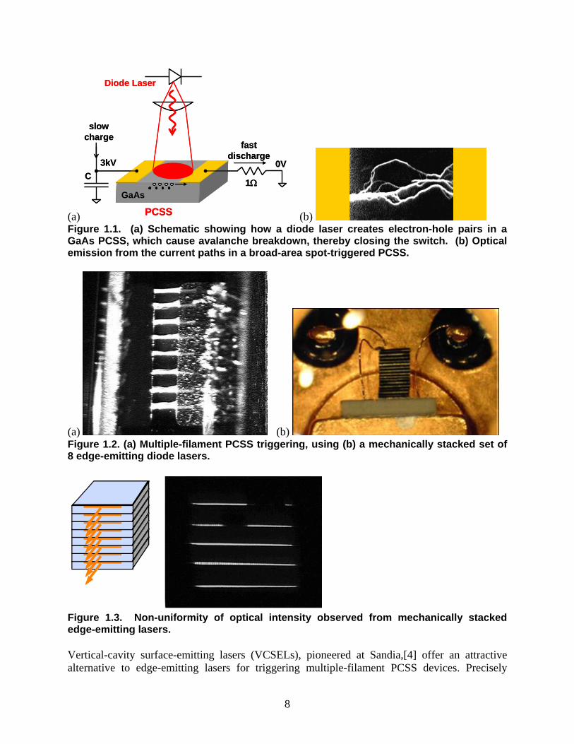
1 LDRD PROJECT INTRODUCTION 1.1 LDRD Project Overview Photoconductive semiconductor switch (PCSS) devices offer advantages of high voltage operation (multi-kV), optical isolation, triggering with laser pulses that cannot occur accidentally in nature, low cost, high speed, small size, and radiation hardness. PCSS devices are candidates for an assortment of potential applications that require multi-kA switching of current. The key to increasing the switching capacity of PCSS devices to 5kV/5kA and higher is to distribute the current in multiple parallel line filaments triggered by an array of high-brightness line-shaped illuminators.[1] Commercial mechanically-stacked edge-emitting lasers have been demonstrated to trigger multiple filaments, but they are difficult to scale and manufacture with the required uniformity. As a promising alternative to multiple discrete edge-emitting lasers, a single wafer of vertical-cavity surface-emitting lasers (VCSELs) can be lithographically patterned to achieve the desired layout of parallel line-shaped emitters, in which adjacent lasers utilize identical semiconductor material and thereby achieve a degree of intrinsic optical uniformity.[2] Under this LDRD project, we have fabricated arrays of uncoupled circular-aperture VCSELs to approximate a line-shaped illumination pattern, achieving optical fill factors ranging from 2% to 30%. We have applied these VCSEL arrays to demonstrate single and dual parallel line-filament triggering of PCSS devices.[3] Moreover, we have developed a better understanding of the illumination requirements for stable triggering of multiple-filament PCSS devices using VCSEL arrays. We have found that reliable triggering of multiple filaments requires matching of the turn-on time of adjacent VCSEL line-shaped-arrays to within approximately 1 ns. Additionally, we discovered that reliable triggering of PCSS devices at low voltages requires more optical power than we obtained with our first generation of VCSEL arrays. A second generation of higher-power VCSEL arrays was designed and fabricated at the end of this LDRD project, and testing with PCSS devices is currently underway (as of September 2008). 1.2 Technical Problem and Approach PCSS devices hold off multi-kV potentials between two electrodes on a GaAs wafer until an incident laser pulse triggers the formation of a conducting filament between the electrodes, as illustrated in Figure 1.1. However, the current carried by this filament must be limited to avoid damage to the electrodes. Recently, PCSS devices with multi-kA current carrying capacity were demonstrated by triggering controlled multiple filaments using edge-emitting laser diode arrays, as shown in Figure 1.2.[1] This proof-of-concept demonstration established a path for scalability to yet higher current/power levels needed for advanced applications. However, spatial non-uniformities in the optical output of the mechanically-stacked edge-emitting laser arrays, shown in Figure 1.3, limited the number of stable filaments that could be achieved, and yields and scalability of such stacked arrays were inherently poor.
8
(a)
Diode Laser
3kV 0V
1
PCSS
GaAs
C
slowcharge
fastdischarge
Diode Laser
3kV 0V
1
PCSS
GaAs
C
slowcharge
fastdischarge
(b) Figure 1.1. (a) Schematic showing how a diode laser creates electron-hole pairs in a GaAs PCSS, which cause avalanche breakdown, thereby closing the switch. (b) Optical emission from the current paths in a broad-area spot-triggered PCSS.
(a) (b) Figure 1.2. (a) Multiple-filament PCSS triggering, using (b) a mechanically stacked set of 8 edge-emitting diode lasers.
Figure 1.3. Non-uniformity of optical intensity observed from mechanically stacked edge-emitting lasers. Vertical-cavity surface-emitting lasers (VCSELs), pioneered at Sandia,[4] offer an attractive alternative to edge-emitting lasers for triggering multiple-filament PCSS devices. Precisely

9
stacking and bonding many edge-emitting laser chips is difficult and costly. In contrast, VCSEL technology is inherently amenable to the formation of 2-D arrays of lasers on a single chip. The VCSEL array patterns are defined lithographically in a single die for ease of packaging, eliminating critical mechanical alignment, and allowing flexible definition of the 2-D illumination profile.[2] The challenge is to fabricate VCSELs with very high aspect ratio line-shaped apertures (on the order of 5 by 500 microns) that exhibit very uniform intensity along the length of the line during a short (10-ns) drive pulse. Before starting this LDRD, we fabricated a line-shaped 3 by 500-micron aperture VCSEL, but the device exhibited highly non-uniform output intensity, as shown in Figure 1.4, due to the hundreds of transverse spatial modes available in the long dimension of the aperture.
Figure 1.4. Photograph of non-uniform optical emission from a line-shaped VCSEL aperture measuring 3 by 500 microns. In order to solve the problem of non-uniform optical intensity, we chose for this LDRD to pursue line-shaped arrays of VCSELs, such that periodic variations in the refractive index assure optical confinement and hence a limited number of well defined optical modes. Figure 1.5 shows an early array of VCSELs that demonstrate the concept. Selective oxidation of AlAs was used to produce a low-index aluminum oxide layer that surrounds each emitting aperture, thus producing several optically confined VCSELs. In order to reliably trigger PCSS devices, very high optical power levels must be produced in a 10 ns optical pulse with fast rise time. Thus, major objectives of this LDRD project were to produce arrays of VCSELs exhibiting uniform output power, high output power, high efficiency, and fast turn-on response.
Figure 1.5. Line-shaped array of oxide-confined VCSELs.
10
2 VCSELS FOR PCSS TRIGGERING 2.1 Introduction In the first year of this LDRD, the laser development effort was directed towards providing well behaved VCSELs for use in initial PCSS triggering experiments to better understand the illumination requirements. We focused on the fabrication and characterization of uncoupled linear arrays of VCSELs having optical fill factors between 2 and 20%. For many years, we have produced linear VCSEL arrays with a 250-um center-to-center device pitch, because this spacing matches the pitch of standard fiber arrays, such as commercial 1x12 fiber arrays. Thus, our first VCSEL arrays were produced using our existing 1x4 VCSEL mask set that contained 1x4 and 1x8 arrays of VCSELs on a 250-um pitch. Because we anticipated the need for as many photons as possible from each VCSEL in the array, we chose to fabricate VCSELs with relatively large active aperture diameters in the range of 10 um, rather than our historically typical aperture diameters near 5 um. 2.2 Early VCSEL Arrays Figure 2.1(a) shows an uncoupled linear VCSEL array that was fabricated in FY06 for PCSS triggering experiments. There are 8 VCSELs in the array, each having an optical aperture of 10 microns, arranged on a 250-micron pitch, yielding an optical fill factor of 4%. The illuminated VCSELs, shown in Figure 2.1(b), exhibited an intensity variation under 10%, thereby accomplishing our first major milestone.
(a) (b) Figure 2.1. (a) Fabricated 8-element uncoupled VCSEL array. (b) Illuminated 8-element VCSEL array. The VCSEL arrays shown in Figure 2.1, from wafer EMC7593, were specifically designed to yield high slope efficiency, since we anticipated that PCSS triggering would require high optical power. Subsequently we fabricated additional VCSEL arrays, from wafer EMC7658, on conducting (n-type) GaAs substrates and employed a common cathode back-side metal contact to improve current uniformity within the 10-micron VCSEL apertures and provide higher current handling capability. The VCSEL array shown in Figure 2.1(b) was driven with a 310-V 10-ns pulse from a 50-ohm source. The parallel resistance of the 8 VCSELs is approximately 5 ohms, from which we estimate a total current supplied to the array of 5.6 A (310V/55ohm). Based on the measured 0.7 W/A slope efficiency of these VCSELs, we estimate a peak power of 3.9 W during the 10-ns pulse, yielding an optical pulse energy of 39 nJ. The actual measured optical pulse energy collected by the imaging optics was 4 nJ. The ~10% lens coupling efficiency is reasonable given the imaging requirements for illuminating the PCSS gap with all eight emitters in the VCSEL array. For comparison, edge-emitting lasers have been used to reliably trigger PCSS devices

11
with optical pulse energies of 500 nJ. Thus, we desire at least an order of magnitude more power from the VCSELs. Of particular concern is the large current density that is being pushed through the VCSEL apertures. An obvious means of increasing the output power without increasing the current density is to increase the fill factor of the electrical current apertures. 2.3 PCSS Triggering with VCSELs The main objective in FY06 was to develop a better understanding of the illumination requirements for stable triggering of multiple-filament PCSS devices. To this end, we tested PCSS devices with arrays of conventional uncoupled VCSELs to determine minimum output power levels required for filament formation. The PCSS test setup was modified, as shown in Figure 2.2(a), to accommodate VCSEL triggering experiments. A single 8-element VCSEL array, described in the section above, was mounted onto the high-voltage RF connector that was used in previous experiments with edge-emitting lasers to trigger PCSS devices. The mounted and wire bonded VCSEL array is shown in Figure 2.2(b).
(a) (b) Figure 2.2. (a) Modified PCSS test setup. (b) High-voltage RF connector with VCSEL array mounted and wire bonded. As described in the previous section, the VCSEL was driven with a 310-V 10-ns pulse from a 50-ohm source, yielding an optical pulse energy of 4 nJ incident on the PCSS device. Figure 2.3(a) shows a top view of the PCSS device, on which the imaged VCSEL array is illustrated to bridge the gap between the two electrodes. The PCSS device was hooked to a short microstrip line (C=0.3 nF) which was charged to 7 kV. The VCSEL pulse creates sufficient electron-hole pairs in the PCSS device to cause electrical breakdown, which was observed in Figure 2.3(b) by optical emission from the current filament formed in the GaAs substrate from recombination of the avalanche-generated electron-hole pairs. As desired, the filament follows the path defined by the imaged VCSEL array.

12
(a) (b) Figure 2.3. . (a) Top view of PCSS device illustrating how the VCSEL array is imaged to fill the gap between the two electrodes. (b) Top view of PCSS device showing optical emission from a filament triggered using an 8-element VCSEL array. Figure 2.4 shows the PCSS switching waveforms (voltage and current) observed during the VCSEL triggered breakdown. The oscillations observed in Figure 2.4 are consistent with a low on-resistance of the switched PCSS device, causing the circuit to be under-damped. While we were pleased to have demonstrated PCSS triggering using a VCSEL array early in the first year of this LDRD, we also identified that significant work lay ahead to achieve the higher optical pulse energies necessary to generate multiple parallel filaments, without destroying the VCSELs due to excessive drive current density.
-6
-4
-2
0
2
4
6
8
-1
-0.5
0
0.5
1
1.5
5 10-8 1 10-7 1.5 10-7 2 10-7 2.5 10-7
Sw
itch
ed
Vo
lta
ge
(K
V) S
witch
ed
Cu
rren
t (A)
time (s) Figure 2.4. PCSS switching voltage and current waveforms observed during the discharge of a short microstrip line (C=0.3nF) charged to 7kV. In summary, we fabricated uncoupled VCSEL arrays and demonstrated triggering of PCSS devices using these arrays. The successful VCSEL line triggering of a PCSS confirmed the technical viability of our approach and the decision to further develop this technology as originally planned in the LDRD proposal.

13
2.4 High Efficiency VCSELs Although we were able to trigger a PCSS filament with as little energy as 4 nJ, more reliable triggering at lower voltage levels requires on the order of 500 nJ of optical pulse energy. Thus, we turned our attention to increasing the efficiency of our VCSELs to deliver more optical output energy for the same input electrical energy. We fabricated a new batch of high efficiency VCSELs from a Sandia grown VCSEL epitaxial structure (wafer EMC7551) that was designed for high efficiency. The design differed from a standard VCSEL primarily in terms of doping levels, which were lower to minimize free-carrier optical absorption, and the number of output coupling DBR periods, which were reduced from 21 to 19 to increase the output coupling percentage relative to the internal optical losses. We note that the two design changes mentioned above were intended to increase the slope efficiency of the VCSEL, which is the quickest path to increasing the electrical to optical efficiency. However, we note that an additional opportunity for optimization is to lower the clamped voltage drop as much as possible, to reach the theoretical minimum value equal to the photon energy voltage drop (1.46 V).
Figure 2.5. Output power and voltage versus current for several VCSELs having different oxide aperture diameters (indicated by labels in figure). Figure 2.5 shows our standard VCSEL characterization data: output power and voltage versus input current, obtained from 4 different VCSELs on the same wafer with different oxide optical aperture sizes (3.5, 4.5, 6.5, and 8.5 microns). The notable features in Figure 2.5 are that the smaller aperture VCSELs have lower threshold currents, higher series resistance (slope of V versus I curve), and exhibit output power “roll-over” due to self heating at lower current and power levels. Figure 2.6 shows the VCSEL output power (again) and efficiency versus input current, again for the same series of oxide aperture sizes as shown in the previous figure. It is clear that the larger aperture sizes achieved the highest output power and efficiency. In particular, we note that the

14
6.5-um aperture device achieved the highest efficiency (36%) at an output power level of 4 mW. At higher output power levels, the 8.5-um aperture VCSEL is more efficient, achieving an efficiency of 31% at an output power level of 12 mW. We present additional data and analysis below to determine the best path forward to increase both efficiency and output power.
Figure 2.6. Output power and efficiency versus current for several VCSELs having different oxide aperture diameters (indicated by labels in figure). As mentioned above, the slope efficiency above threshold is the parameter of highest interest for achieving high efficiency VCSELs. For generality and ease of understanding, we have divided the slope efficiency values (mW/mA) by the theoretical maximum value (1.46 mW/mA) to obtain the differential quantum efficiency (DQE). The DQE and threshold current versus oxide aperture diameter are shown in Figure 2.7 for the same 4 VCSELs as discussed previously. As expected, the DQE is reduced at smaller aperture sizes, which again shows that aperture diameters above 6 um are best, achieving DQEs of approximately 63%. We believe that the DQE can be increased to near 80% with further optimization.
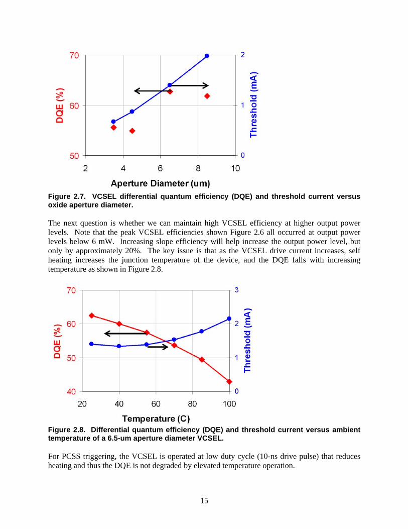
15
Figure 2.7. VCSEL differential quantum efficiency (DQE) and threshold current versus oxide aperture diameter. The next question is whether we can maintain high VCSEL efficiency at higher output power levels. Note that the peak VCSEL efficiencies shown Figure 2.6 all occurred at output power levels below 6 mW. Increasing slope efficiency will help increase the output power level, but only by approximately 20%. The key issue is that as the VCSEL drive current increases, self heating increases the junction temperature of the device, and the DQE falls with increasing temperature as shown in Figure 2.8.
Figure 2.8. Differential quantum efficiency (DQE) and threshold current versus ambient temperature of a 6.5-um aperture diameter VCSEL. For PCSS triggering, the VCSEL is operated at low duty cycle (10-ns drive pulse) that reduces heating and thus the DQE is not degraded by elevated temperature operation.
16
2.5 Summary In the first year (FY06) of this LDRD, we focused on developing a better understanding of the illumination requirements for stable triggering of multiple-filament PCSS devices. To this end, we tested PCSS devices with arrays of conventional uncoupled VCSELs to determine minimum output power levels required for filament formation. Although we succeeded in demonstrating PCSS triggering using VCSEL arrays, the optical pulse energy obtained (4 nJ) was approximately 2 orders of magnitude lower than desired. One path to increase the optical pulse energy is to increase the intrinsic efficiency of each VCSEL at converting electrical to optical power. We fabricated new VCSEL wafers specifically designed to yield higher optical efficiency, and thereby achieved a peak efficiency of 36% at 4 mW of output power from a 6.5-um aperture VCSEL. At higher output power levels, the 8.5-um aperture VCSEL is more efficient, achieving an efficiency of 31% at an output power level of 12 mW. A systematic optimization of doping profiles and internal optical losses would be required to further improve the VCSEL efficiency beyond 36%. A second path to increase the optical pulse energy is to increase the number of VCSELs in the array. The following sections discuss work in this direction.

17
3 FIRST GENERATION VCSEL ARRAYS 3.1 Introduction In order to obtain higher optical pulse energies required to trigger PCSS devices more reliably, we designed a new VCSEL mask set in FY06 to increase the number of VCSEL emitters in the array by a factor of 5. This section describes the new mask set, the VCSEL performance, and triggering of PCSS devices using these high-density linear VCSEL arrays. 3.2 VPCSS1 Mask Layout We called the new mask set VPCSS1, which is an abbreviation indicating that these are VCSELs designed specifically for triggering PCSS devices. On the VPCSS1 mask set, we retained the 1-D array layout from previous mask sets, but decreased the VCSEL pitch from 250 to 50 um, as shown in Figure 3.1. The number of VCSELs in a nearly 2-mm long array was thus increased from 8 to 37, yielding a 5-fold increase in optical fill factor and total power output.
Figure 3.1. Higher density VCSEL arrays on VPCSS1 mask set. Figure 3.2 shows the unit cell (or die) that is repeated across the 75mm x 75mm field of the VPCSS1 mask plates. Each die measures 5mm wide by 4.5mm tall and contains 12 linear arrays of 37 VCSELs and 3 linear arrays of 17 VCSEL, all on a 50-um pitch. The labels shown in Figure 3.2, such as “38C”, indicate that the diameter of each VCSEL mesa in that particular array is 38 microns. The VCSEL current apertures are intended to be oxidized for a time sufficient to fully “close” the aperture on a 28-um-diameter mesa, in which case a 38-um-diameter mesa will have a VCSEL aperture diameter of 10 um. In the case of quarter wafer EMC7551-A, subsequently used for PCSS triggering, the 29.5-um-diameter mesa was closed, so the 38-um-diameter mesas had VCSEL aperture diameters of 8.5 um. The metal contact ring on the top of each mesa had a width of 9 microns, set back 2 microns from the edge of the mesa. Thus the top metal outer diameter is 4 um smaller than the mesa diameter, and the inner diameter

18
is 22 um smaller than the mesa diameter. For a 38-um mesa diameter, the top metal inner diameter is 16 um, which is sufficiently larger than the intended VCSEL current aperture diameter of 10 um. The center column of 6 VCSEL arrays shown in Figure 3.2 was intended to test the effect of varying the VCSEL aperture diameter from 4 to 14 um. The right column of 6 VCSEL arrays is arranged in 3 pairs, where each pair is intended for dual-filament triggering of a PCSS device, with VCSEL aperture diameters of nominally 8, 10, or 12 um for the 3 pairs.
Figure 3.2. VPCSS1 die layout measuring 5mm by 4.5mm. The remaining VCSELs and diagnostic structures shown in the die layout of Figure 3.2 are intended for obtaining quantitative data regarding the epitaxial material, device fabrication steps, and high-speed device response. In particular, we note that the TLM structures tell us the sheet resistance of the doped semiconductor layers and the contact resistance of the metal-to-semiconductor ohmic contacts. The variable diameter VCSELs V30 to V80 allow us to test high-speed response versus VCSEL aperture diameter. And the VNA calibration structures allow us to calibrate ground-signal-ground (GSG) wafer probe impedance measurements made using a vector network analyzer (VNA), typically up to frequencies near 20 GHz. A single linear VCSEL array intended for PCSS triggering is shown schematically in Figure 3.3. As seen in the figure, the VPCSS1 mask set allows processing of VCSEL epitaxy grown on semi-insulating GaAs substrates, which requires top-side anode and cathode contact pads. The

19
anode and cathode contact pads are designed to be wide enough to achieve low electrical resistance and provide ample space for the attachment of multiple gold wire or ribbon bonds. As shown by the partial equivalent circuit at the right side of Figure 3.3, the 37 VCSELs in the array are electrically connected in parallel by the bond pad metal (green).
Figure 3.3. Linear array of 37 VCSELs on VPCSS1 mask. 3.3 VPCSS1 Laser Performance Figure 3.4 shows a 37-element linear array of VCSELs on quarter wafer EMC7551-A driven CW with 80 mA of current through two needle probes. The CW laser performance of single VCSELs versus aperture diameter was reported already in section 2.4 on high-efficiency VCSELs. The measured CW efficiencies up to 37% are the highest achieved at Sandia in the last 10 years, and may be the highest ever achieved at Sandia at a wavelength of 850 nm.[5]
Figure 3.4. Linear array of 8.5-um VCSELs driven CW with 80 mA of current. For PCSS triggering applications, the 37-element VCSEL array shown in Figure 3.4 was driven with a 275-V 10-ns pulse from a 50-ohm source. The parallel resistance of the 37 VCSELs was approximately 0.5 ohms, from which we estimate a total current supplied to the array of 10.9A (275V*2/50.5). The actual measured optical pulse energy collected by the imaging optics was 120 nJ, which represents a 30-fold improvement relative to the first VCSEL arrays used to trigger PCSS devices in FY06. The high optical coupling efficiency from the VCSEL array to the PCSS device was accomplished by using a short focal length lens (2.75 mm) with very high numerical aperture (0.65), given the imaging requirements for illuminating the PCSS gap with all 74 emitters of the arrays. For comparison, edge-emitting lasers have been used to reliably trigger PCSS devices with optical pulse energies of 500 nJ. Thus, we still desired at least 4 times more energy from the VCSEL arrays for highly reliable PCSS triggering.
20
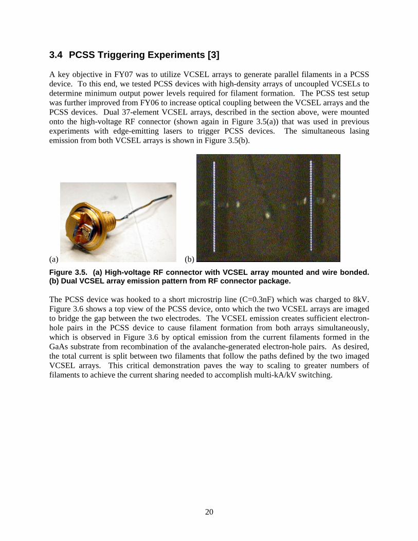
3.4 PCSS Triggering Experiments [3] A key objective in FY07 was to utilize VCSEL arrays to generate parallel filaments in a PCSS device. To this end, we tested PCSS devices with high-density arrays of uncoupled VCSELs to determine minimum output power levels required for filament formation. The PCSS test setup was further improved from FY06 to increase optical coupling between the VCSEL arrays and the PCSS devices. Dual 37-element VCSEL arrays, described in the section above, were mounted onto the high-voltage RF connector (shown again in Figure 3.5(a)) that was used in previous experiments with edge-emitting lasers to trigger PCSS devices. The simultaneous lasing emission from both VCSEL arrays is shown in Figure 3.5(b).
(a) (b)
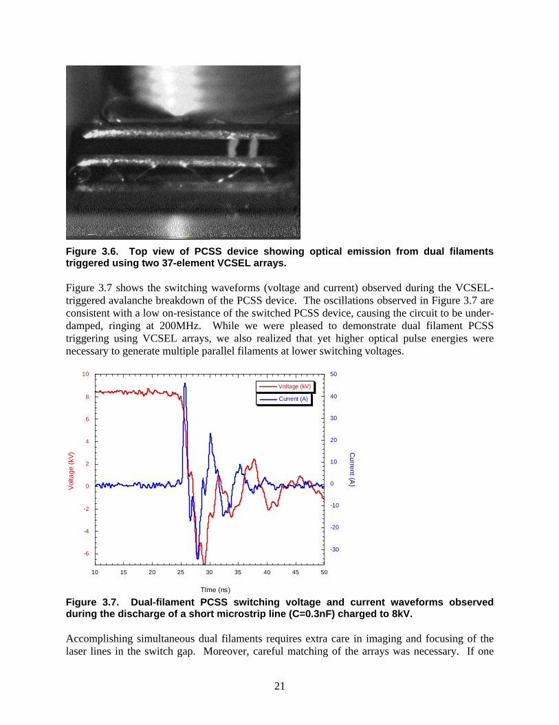
Figure 3.5. (a) High-voltage RF connector with VCSEL array mounted and wire bonded. (b) Dual VCSEL array emission pattern from RF connector package. The PCSS device was hooked to a short microstrip line (C=0.3nF) which was charged to 8kV. Figure 3.6 shows a top view of the PCSS device, onto which the two VCSEL arrays are imaged to bridge the gap between the two electrodes. The VCSEL emission creates sufficient electron-hole pairs in the PCSS device to cause filament formation from both arrays simultaneously, which is observed in Figure 3.6 by optical emission from the current filaments formed in the GaAs substrate from recombination of the avalanche-generated electron-hole pairs. As desired, the total current is split between two filaments that follow the paths defined by the two imaged VCSEL arrays. This critical demonstration paves the way to scaling to greater numbers of filaments to achieve the current sharing needed to accomplish multi-kA/kV switching.
21
Figure 3.6. Top view of PCSS device showing optical emission from dual filaments triggered using two 37-element VCSEL arrays. Figure 3.7 shows the switching waveforms (voltage and current) observed during the VCSEL-triggered avalanche breakdown of the PCSS device. The oscillations observed in Figure 3.7 are consistent with a low on-resistance of the switched PCSS device, causing the circuit to be under-damped, ringing at 200MHz. While we were pleased to demonstrate dual filament PCSS triggering using VCSEL arrays, we also realized that yet higher optical pulse energies were necessary to generate multiple parallel filaments at lower switching voltages.
-6
-4
-2
0
2
4
6
8
10
-30
-20
-10
0
10
20
30
40
50
10 15 20 25 30 35 40 45 50
Voltage (kV)
Current (A)
Vo
ltag
e (k
V) C
urren
t (A)
TIme (ns) Figure 3.7. Dual-filament PCSS switching voltage and current waveforms observed during the discharge of a short microstrip line (C=0.3nF) charged to 8kV. Accomplishing simultaneous dual filaments requires extra care in imaging and focusing of the laser lines in the switch gap. Moreover, careful matching of the arrays was necessary. If one

22
filament forms before the other, the voltage necessary for generating lock-on at the other laser line is dissipated. Therefore, for two filaments to form, the delay time in filament formation must be the same for both laser lines. Figure 3.8 shows the lock-on delay time (relative to a fixed scope trigger signal) as a function of charge voltage on the PCSS. As expected, the delay time decreases as the voltage is increased until it is too close to the self-break voltage (~10kV in this case), and flattens out at the higher voltages. At these higher voltages, the timing jitter is also lower, and it becomes easier to trigger two filaments consistently. In Figure 3.8(a), the arrays are well-matched and are able to trigger dual filaments reliably at the higher charge voltages. In Figure 3.8(b), even though each array is itself able to generate a line filament, the consistent (~2ns) mismatch in delay prevents dual filament formation.
0
5
10
15
20
25
0 2 4 6 8 10
Re
lativ
e L
ock-
On
De
lay
(ns
)
Charge Vo ltage (kV)
Charge Voltage (kV)
Re
lati
ve
Lo
ck
-On
De
lay
(n
s)
Well-matched arrays
0
5
1 0
1 5
2 0
2 5
3 0
0 2 4 6 8 10
Re
lativ
e L
ock-
On
De
lay
(ns)
Charge Voltag e (kV)Charge Voltage (kV)
Re
lati
ve
Lo
ck
-On
De
lay
(n
s)
Poorly matched arrays
(a) (b)
0
5
10
15
20
25
0 2 4 6 8 10
Re
lativ
e L
ock-
On
De
lay
(ns
)
Charge Vo ltage (kV)
Charge Voltage (kV)
Re
lati
ve
Lo
ck
-On
De
lay
(n
s)
Well-matched arrays
0
5
10
15
20
25
0 2 4 6 8 10
Re
lativ
e L
ock-
On
De
lay
(ns
)
Charge Vo ltage (kV)
Charge Voltage (kV)
Re
lati
ve
Lo
ck
-On
De
lay
(n
s)
Well-matched arrays
0
5
1 0
1 5
2 0
2 5
3 0
0 2 4 6 8 10
Re
lativ
e L
ock-
On
De
lay
(ns)
Charge Voltag e (kV)Charge Voltage (kV)
Re
lati
ve
Lo
ck
-On
De
lay
(n
s)
Poorly matched arrays
0
5
1 0
1 5
2 0
2 5
3 0
0 2 4 6 8 10
Re
lativ
e L
ock-
On
De
lay
(ns)
Charge Voltag e (kV)Charge Voltage (kV)
Re
lati
ve
Lo
ck
-On
De
lay
(n
s)
Poorly matched arrays
(a) (b) Figure 3.8. Lock-on delay of (a) well-matched and (b) poorly matched VCSEL arrays. 3.5 Summary In FY07, we increased the optical energy from each VCSEL array 30-fold, from 4 nJ to 120 nJ in a 10-ns pulse. A factor of 5 improvement was due to the higher density of VCSELs in the array. A factor of 2 improvement was due to higher electrical-to-optical efficiency from each VCSEL. And the remaining factor of 3 improvement was due to better imaging optics between the VCSEL array and the PCSS device. The successful dual-line triggering of PCSS devices with VCSEL arrays further confirmed the technical viability of our approach and the decision to continue developing the VCSEL triggering technology.

23
4 SECOND GENERATION VCSEL ARRAYS 4.1 Introduction Although the optical pulse energy from each VCSEL array was increased 30-fold in FY07, another 4-fold increase was required to achieve energies sufficient to reliably trigger PCSS devices at lower voltages. In FY08, we further increased the number of VCSEL emitters in each line-shaped array 2-fold by making two-dimensional 2 x 37 arrays of VCSELs. In addition, the active aperture diameter of each VCSEL in the array was approximately doubled, which quadrupled the active region area and was thus expected to provide up to a 4-fold increase in power from each VCSEL. The design and performance of these new VCSELs is documented in this section. Because the VCSEL device fabrication was not finished until late in FY08, the new arrays were not ready for PCSS triggering experiments in time for inclusion in this report. 4.2 VPCSS2 Mask Layout As in FY07, we further increased the number of VCSELs within each line-shaped emitter array as a means of increasing the total output power. Because we desired sufficient space around each VCSEL mesa for gas flow during the selective oxidation process step, we did not feel comfortable packing the approximately 40-um-diameter VCSEL mesas any closer together than the 50-um pitch employed on the VPCSS1 mask set, which left a gap of only 10 um between adjacent VCSEL mesas. Thus, we chose to expand the 1-D array of VCSELs to a 2-D array, consisting of 2 rows of 37 VCSELs, as shown in Figure 4.1.
Figure 4.1. Line-shaped array of 2 x 37 VCSELs on the VPCSS2 mask set. In addition to doubling the number of VCSELs within each array on the new VPCSS2 mask set, we have also almost doubled the diameter of each VCSEL aperture, which nearly quadruples the active region area and thus is expected to provide up to a 4-fold increase in output power from each VCSEL. For visual comparison, Figure 4.2 shows partial arrays of 36-um-mesa VCSELs on the VPCSS1 and VPCSS2 mask sets. The top metal ring width has decreased from 9 um to 6 um in order to increase the allowable oxide aperture diameter, nominally indicated by the blue dotted lines in Figure 4.2. For the 36-um mesas shown in Figure 4.2, the active oxide aperture diameter has increased from 8 um to 14 um (nominally). Because of current crowding at the edge of the active region aperture, we do not expect the output power to scale linearly with the aperture area. However, it should scale at least as fast as the diameter, so we expect at least a factor of two increase in output power. Thus, doubling the number of VCSELs per array and at

24
least doubling the power of each VCSEL should provide a 4-fold increase in output optical power, as required for reliable triggering of PCSS devices.
Figure 4.2. Comparison of oxide aperture (blue dotted lines) relative to top metal and 36-um-diameter top mesas on (a) VPCSS1 and (b) VPCSS2 mask sets. Figure 4.3 shows the unit cell (or die) that is repeated across the 75mm x 75mm field of the VPCSS2 mask plates. Each die measures 5mm wide by 4.5mm tall and contains 12 linear arrays of 2 x 37 VCSELs and 3 linear arrays of 2 x 17 VCSEL. Within one array, the VCSELs are positioned on an x-pitch of 50 um, and the y-pitch between the two staggered rows is 43 um. The labels shown in Figure 4.3, such as “36C”, indicate that the diameter of each VCSEL mesa in that particular array is 36 microns. The VCSEL current apertures are intended to be oxidized for a time sufficient to fully “close” the aperture on a 22-um-diameter mesa, in which case a 36-um-diameter mesa will have a VCSEL aperture diameter of 14 um. In the case of quarter wafer EMC7551-C, processed for PCSS triggering experiments in 2008, the 24-um-diameter mesa was closed, so the 36-um-diameter mesas had VCSEL aperture diameters of 12 um. The metal contact ring on the top of each mesa had a width of 6 microns, set back 2 microns from the edge of the mesa. Thus the top metal outer diameter is 4 um smaller than the mesa diameter, and the inner diameter is 16 um smaller than the mesa diameter. For a 36-um mesa diameter, the top metal inner diameter is 20 um, which is sufficiently larger than the intended VCSEL current aperture diameter of 14 um. The center column of 6 VCSEL arrays shown in Figure 4.3 was intended to test the effect of varying the VCSEL aperture diameter from 10 to 20 um. The right column of 6 VCSEL arrays is arranged in 2 triplets, where each triplet is intended for triple-filament triggering of a PCSS device, with VCSEL aperture diameters of nominally 14 or 18 um for the 2 triplets.

25
Figure 4.3. VPCSS2 die layout measuring 5mm by 4.5mm. The remaining VCSELs and diagnostic structures shown in the die layout of Figure 4.3 are intended for obtaining quantitative data regarding the epitaxial material, device fabrication steps, and high-speed device response. In particular, we note that the TLM structures tell us the sheet resistance of the doped semiconductor layers and the contact resistance of the metal-to-semiconductor ohmic contacts. The variable diameter VCSELs V20 to V80 allow us to test high-speed response versus VCSEL aperture diameter. And the VNA calibration structures allow us to calibrate ground-signal-ground (GSG) wafer probe impedance measurements made using a vector network analyzer (VNA), typically up to frequencies near 20 GHz. 4.3 VPCSS2 Laser Performance A die (number 457) fabricated using the VPCSS2 mask set on quarter wafer EMC7551-C is shown in Figure 4.4. A 2 x 37 VCSEL array “36B” is shown lasing in Figure 4.5 at a drive current of 400 mA. Because of the increased number of VCSELs that are driven in parallel and the increased aperture diameter (12 um) of each VCSEL, the CW threshold current of this “36B” array is above 100 mA, which is the maximum output of our semiconductor parameter analyzer computer-controlled current source. It appears from the photograph in Figure 4.5 that the output intensity of the lower row of VCSELs is somewhat less than that of the upper row. We anticipated that this might be the case during the mask design, due to the fact that the n-type lower contact metal is only located above the upper row of VCSELs, because the gap between adjacent VCSELs (approximately 10 um) is too narrow to reliably deposit n-contact metal

26
without shorting the VCSEL diodes. However, a slight imbalance in the output intensities of the two rows of VCSELs should be fine, as long as the uniformity along the length of each row is high.
Figure 4.4. Fully fabricated VPCSS2 die on quarter wafer EMC7551-C.
Figure 4.5. A lasing 2 x 37 VCSEL array driven with 400 mA of current. As shown in Figure 4.6, we measured light output versus current from a smaller 2 x 17 array “32A” that reached threshold well within the 100-mA drive limit of our semiconductor parameter analyzer. The current aperture diameter of each VCSEL in this array is 8 um (deduced from measurements that show that the 24-um-diameter mesa is closed). The curve fit in Figure 4.6 shows a slope efficiency from this array of 0.905 W/A, which is equivalent to a differential quantum efficiency of 62% (consistent with FY07 measurements on quarter wafer EMC7551-A). The absolute efficiency of this VCSEL array reaches 22% at 100 mA drive current and increases further at higher drive currents. This preliminary data indicates that under pulsed operation we will obtain the 500-nJ output energy required for reliable PCSS triggering.

27
y = 0.9053x - 46.371
0
10
20
30
40
50
0 20 40 60 80 100
Current (mA)
Po
we
r (m
W)
0
5
10
15
20
25
Eff
icie
nc
y (
%)
Figure 4.6. Optical output power vs. input current for 2 x 17 VCSEL array “32A”. For completeness, the optical output spectrum of one VCSEL in the same “32A” array is shown in Figure 4.7 at a drive current of 80 mA. The fundamental wavelength (the longest wavelength peak in the spectrum) is 848.40 nm at 80 mA (1.932 V) and shifts to 848.95 nm at 160 mA (2.315 V). From the known rate of wavelength shift with junction temperature (0.06 nm/K) we determine that the junction temperature rises by only 9.2 K when the drive current is increased from 80 to 160 mA. As expected for a relatively large-aperture VCSEL, the output spectrum is highly multi-mode, having a width of approximately 2 nm. The larger-diameter VCSELs in the “36B” array exhibit an even broader output spectrum.
-80
-70
-60
-50
-40
-30
-20
830 840 850 860
Wavelength (nm)
Po
we
r (d
Bm
)
Figure 4.7. Optical output spectrum of one VCSEL in a 2 x 17 array “32A” at 80 mA drive. 4.4 Summary The properties of the VCSELs fabricated in FY08 using the VPCSS2 mask set are entirely consistent with our expectations and thus should be highly suited to triggering PCSS devices. We plan to test PCSS triggering using these new VCSEL arrays in September 2008.
28
5 CONCLUSIONS Recently, PCSS devices with multi-kA current carrying capacity were demonstrated by triggering controlled multiple filaments using edge-emitting laser diode arrays. This proof-of-concept demonstration established a path for scalability to yet higher current/power levels needed for potential new applications. However, spatial non-uniformities in the optical output of the mechanically-stacked edge-emitting laser arrays limited the number of stable filaments that could be achieved, and yields and scalability of such stacked arrays were inherently poor. Vertical-cavity surface-emitting lasers (VCSELs), pioneered at Sandia, offer an attractive alternative to edge-emitting lasers for triggering multiple-filament PCSS devices. Precisely stacking and bonding many edge-emitting laser chips is difficult and costly. In contrast, VCSEL technology is inherently amenable to the formation of 2-D arrays of lasers on a single chip. The VCSEL array patterns are defined lithographically on a single chip for ease of packaging, eliminating critical mechanical alignment, and allowing flexible definition of the 2-D illumination profile. The challenge is to fabricate VCSELs with line-shaped output-intensity profiles that exhibit very uniform intensity along the length of the line during a short (10-ns) drive pulse. Over the course of this 3-year LDRD project, we have demonstrated the first line triggering and dual-line triggering of PCSS devices with VCSEL arrays. A consistent challenge throughout the project has been to obtain the 500-nJ output energy per line-shaped VCSEL array in a 10-ns pulse that is required for reliable triggering of PCSS devices. At the end of 3 years of work and two custom mask set designs we have essentially met the optical pulse energy goal. The key technical advances that contributed to our success were: (1) increasing the number of VCSELs per array, (2) increasing the active area and thus output power of each VCSEL in the array, and (3) increasing the slope efficiency of each VCSEL through optimization of the epitaxial structure. Final testing of PCSS device triggering using the newest high-power VCSEL arrays is underway in September 2008. In conclusion, although achieving sufficient optical power from a VCSEL array has been a challenge, we have proved that it can be done. The 2-D scalability of VCSEL arrays is expected to permit PCSS operation at record current levels, which will enable a variety of potential new applications. Moreover, the inherent manufacturability of VCSEL arrays makes the use of high-current PCSS devices more practical than ever.

29
6 REFERENCES
1. A. Mar, G.M. Loubriel, F.J. Zutavern, L.D. Roose, A.G. Baca, G.J. Denison, P.A. Smith, M.W. O'Malley, D.J. Brown, “Fireset applications of improved longevity optically activated GaAs photoconductive semiconductor switches,” IEEE Pulsed Power Plasma Science 2001 Conference, vol. 1, pp. 166-169 (2001).
2. K.M. Geib, K.D. Choquette, D.K. Serkland, A.A. Allerman, T.W. Hargett, “Fabrication and performance of two-dimensional matrix addressable arrays of integrated vertical-cavity lasers and resonant cavity photodetectors,” IEEE Journal of Selected Topics in Quantum Electronics, vol. 8, pp. 943-947 (2002).
3. A. Mar, D.K. Serkland, G.A. Keeler, L.D. Roose, K.M. Geib, G.M. Loubriel, F.J. Zutavern, “Multi-filament triggering of PCSS for high current utilizing VCSEL triggers,” 2007 IEEE Pulsed Power Plasma Science Conference, vol. 1-4, pp. 1000-1003 (2007).
4. K.D. Choquette, K.L. Lear, R.P. Schneider, Jr., K.M. Geib, J.J. Figiel, R. Hull, “Fabrication and performance of selectively oxidized vertical-cavity lasers,” IEEE Photonics Technology Letters, vol. 7, pp. 1237-1239 (1995).
5. K.L. Lear, K.D. Choquette, R.P. Schneider, Jr., S.P. Kilcoyne, K.M. Geib, “Selectively oxidised vertical cavity surface emitting lasers with 50% power conversion efficiency,” Electronics Letters, vol. 31, pp. 208-209 (1995).

30
7 DISTRIBUTION 2 MS1085 Darwin K. Serkland 1742 1 MS1085 Kent M. Geib 1742 1 MS1085 Gregory M. Peake 1742 1 MS1085 Gordon A. Keeler 1742 1 MS1085 G. Ronald Hadley 1742 1 MS1085 Charles T. Sullivan 1742 2 MS1153 Alan Mar 5443 2 MS1153 Guillermo M. Loubriel 5443 1 MS0899 Technical Library 9536 1 MS0123 D. Chavez, LDRD Office 1011
