final report of ldrd project: electromagnetic impulse radar for detection...
TRANSCRIPT

SANDIA REPORTSAND98-0724Unlimited ReleasePrinted March, 1998
FINAL REPORT OF LDRD PROJECT:ELECTROMAGNETIC IMPULSE RADAR FORDETECTION OF UNDERGROUND STRUCTURES
Guillermo Loubriel, John Aurand, Malcolm Buttram, Fred Zutavern, Darwin Brown, andWesley Helgeson
Prepared bySandia National LaboratoriesAlbuquerque, NM 87185-1153for the United States Department of Energyunder contract DE-AC04-94AL85000.

2
Issued by Sandia National Laboratories, operated for the United StatesDepartment of Energy by Sandia Corporation.NOTICE: This report was prepared as an account of work performed by anagency of the United States Government. Neither the United States Govern-ment, nor any agency thereof, nor any of their employees, nor any of theircontractors, subcontractors, or their employees, makes any warranty, expressor implied, or assumes any legal liability or responsibility for the accuracy,completeness, or usefulness of any information, apparatus, product, orprocess disclosed, or represents that its use would not infringe privatelyowned rights. Reference herein to any specific commercial product, process,or service by trade name, trademark, manufacturer, or otherwise, does notnecessarily constitute or imply its endorsement, recommendation, or favoringby the United States Government, any agency thereof or any of theircontractors or subcontractors. The views and opinions expressed herein donot necessarily state or reflect those of the United States Government, anyagency thereof or any of their contractors.

3
SAND 98-0724 DistributionUnlimited Release Category UC-402, 403, 406
PRINTED: March, 1998
FINAL REPORT OF LDRD PROJECT:ELECTROMAGNETIC IMPULSE RADAR FOR DETECTION OF
UNDERGROUND STRUCTURES
Guillermo Loubriel, John Aurand, Malcolm Buttram,Fred Zutavern, Darwin Brown, and Wesley Helgeson
High Power Electromagnetics DepartmentSandia National Laboratories
P. O. Box 5800Albuquerque, NM 87185-1153
Abstract
This report provides a summary of the LDRD project titled: Electromagnetic impulseradar for the detection of underground structures. The project met all its milestones evenwith a tight two year schedule and total funding of $ 400 k. The goal of the LDRD was todevelop and demonstrate a ground penetrating radar (GPR) that is based on high peakpower, high repetition rate, and low center frequency impulses. The idea of this LDRD isthat a high peak power, high average power radar based on the transmission of shortimpulses can be utilized effect can be utilized for ground penetrating radar. This directtime-domain system we are building seeks to increase penetration depth overconventional systems by using: 1) high peak power, high repetition rate operation thatgives high average power, 2) low center frequencies that better penetrate the ground, and3) short duration impulses that allow for the use of downward looking, low flyingplatforms that increase the power on target relative to a high flying platform.Specifically, chirped pulses that are a microsecond in duration require (because it isdifficult to receive during transmit) platforms above 150 m (and typically 1 km) whilethis system, theoretically could be at 10 m above the ground. The power on target decayswith distance squared so the ability to use low flying platforms is crucial to highpenetration. Clutter is minimized by time gating the surface clutter return. Short impulsesalso allow gating (out) the coupling of the transmit and receive antennas.
A transmission line, charged to 100 kV, was discharged with high gain GaAsphotoconductive semiconductor switches (PCSS) into a matched antenna. The design ofthe transmission line was based on calculations of the penetration of differentelectromagnetic waveforms produced by different pulser geometries. To this end, wedeveloped a simple model that includes transmit and receive antenna response,
4
attenuation and dispersion of the electromagnetic impulses by the soil, and target crosssections. Thus, given an initial voltage waveform into the antenna, the programcalculates the return waveform.
The system was used to: 1) measure penetration of the transmit pulse through large (2feet thick) concrete blocks, 2) measure returns from targets in air (no penetration), 3)measure returns from targets obscured by concrete.
The enabling technology for the transmitter is high gain GaAs photoconductivesemiconductor switches. These switches can hold off high voltages in the “off” state,and, when triggered with small laser diodes and laser diode arrays, have fast risetime, andlow jitter. An important accomplishment of this LDRD is that we were able to triggertwo switches, at opposite ends of a transmission line, with low enough jitter to achieve abipolar waveform. At the start of tests, we only achieved a bipolar waveform once every10 pulses. By the end of the LDRD we obtained very reproducible waveforms. This wasachieved through a combination of multiple laser diode triggering and forcing the light toform lines on the switch instead of round spots that are the typical pattern from the opticalfibers.
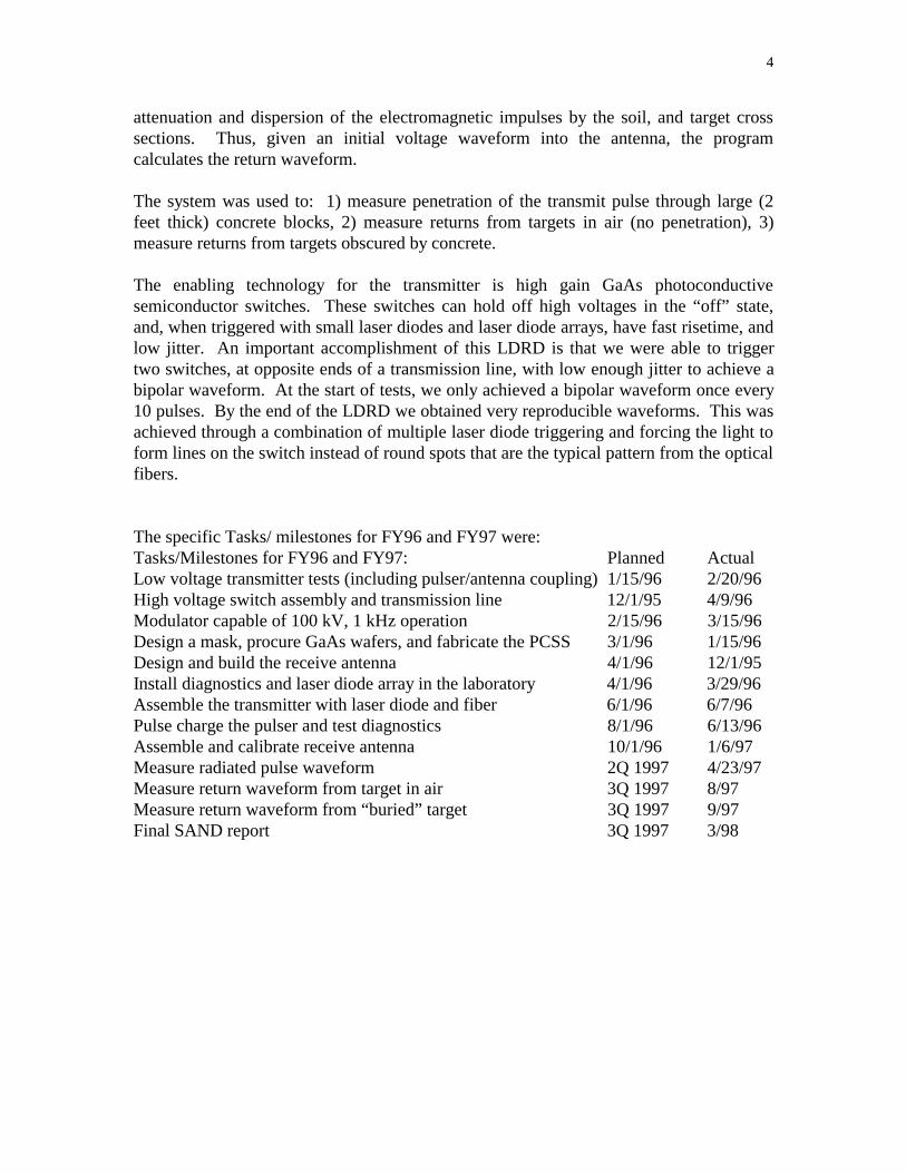
The specific Tasks/ milestones for FY96 and FY97 were:Tasks/Milestones for FY96 and FY97: Planned ActualLow voltage transmitter tests (including pulser/antenna coupling) 1/15/96 2/20/96High voltage switch assembly and transmission line 12/1/95 4/9/96Modulator capable of 100 kV, 1 kHz operation 2/15/96 3/15/96Design a mask, procure GaAs wafers, and fabricate the PCSS 3/1/96 1/15/96Design and build the receive antenna 4/1/96 12/1/95Install diagnostics and laser diode array in the laboratory 4/1/96 3/29/96Assemble the transmitter with laser diode and fiber 6/1/96 6/7/96Pulse charge the pulser and test diagnostics 8/1/96 6/13/96Assemble and calibrate receive antenna 10/1/96 1/6/97Measure radiated pulse waveform 2Q 1997 4/23/97Measure return waveform from target in air 3Q 1997 8/97Measure return waveform from “buried” target 3Q 1997 9/97Final SAND report 3Q 1997 3/98

5
CONTENTS
Section
1.0 SUMMARY/ CONCLUSION 61.1 GOALS AND TASKS 61.2 RESULTS 61.3 CONCLUSIONS 10
2.0 INTRODUCTION: HIGH GAIN GaAs SWITCHES 112.1 HIGH GAIN GaAs SWITCHES 112.2 DEVICE DESCRIPTION 112.3 HIGH GAIN 132.4 CURRENT FILAMENTS 142.5 DEVICE LONGEVITY 15
3.0 CALCULATIONS OF GROUND PENETRATION 173.1 MODEL OF ELECTROMAGNETIC
GROUND PENETRATION 183.2 RESULTS FROM THE MODEL 21
4.0 RADAR TRANSMITTER 224.1 MODULATOR 224.2 PULSE FORMING LINE 264.3 LASER DIODE ARRAYS AND ELECTRONICS 294.4 ANTENNA AND IMPEDANCE MATCHING SECTION 30
5.0 SYSTEM TESTS 355.1 SYSTEM TESTS 355.2 TESTS WITH UN-OBSCURED TARGETS 385.3 PENETRATION THROUGH CONCRETE 41
6.0 REFERENCES 43

6
1.0 SUMMARY/ CONCLUSION
This section summarizes the goals of this project, the tasks required to meet the goals asoutlined in the original LDRD proposal, and the results and conclusions of the LDRD.
1.1 TASKS
The goal of the LDRD was to develop and demonstrate a ground penetrating radar (GPR)that is based on high peak power, high repetition rate, and low center frequency impulses.The task are:Task:Task 0—Calculations of electromagnetic penetration into soil and radar returnsTask 1--Low voltage transmitter tests (including pulser/antenna coupling)Task 2--High voltage switch assembly and transmission lineTask 3--Modulator capable of 100 kV, 1 kHz operationTask 4--Design a mask, procure GaAs wafers, and fabricate the PCSSTask 5--Design and build the receive antennaTask 6--Install diagnostics and laser diode array in the laboratoryTask 7--Assemble the transmitter with laser diode and fiberTask 8--Pulse charge the pulser and test diagnosticsTask 9--Assemble and calibrate receive antennaTask 10--Measure radiated pulse waveformTask 11--Measure return waveform from target in airTask 12--Measure return waveform from “buried” targetTask 13--Final SAND report
1.2 RESULTS
Task 0- Calculations of electromagnetic penetration into soil and radar returns: This taskwas added at the beginning of the project to improve on initial back-of-the-envelopecalculations of system requirements. We developed a model for GPR in which we canvary the initial voltage pulse into the antenna, and includes the measured antenna transferfunction, the transmission of the electromagnetic waves on entering (and exiting) soil,attenuation and dispersion by the soil (real soils with varying water content), and thecross section of the target. The model assumes normal incidence into soil and target. Themodel showed that high peak power impulses do penetrate into soils with some watercontent in such a way that targets buried down to 10 m could be detected.
Task 1- Low voltage transmitter tests: An existing antenna was tested at low voltages todetermine its characteristics, especially at low frequencies. We used different techniques(frequency-domain and time-domain) to characterize both the input reflection and thetransmitting/radiating performance of the antenna. The antenna acts as a derivativeantenna almost exclusively. Its input match is best at 50 Ω and its transfer function has a

7
low frequency roll-off of about 70 MHz (meaning that the antenna does not radiateeffectively below 70 MHz). For this reason we modified the design of the pulse formingline to have 50 Ω impedance and for it to produce a bipolar pulse with a 6.3 ns period (sothat its peak spectral content is at 133 MHz). We also built and calibrated a voltagedivider to measure the voltage wave into the antenna (at the feed point).
Task 2- High voltage switch assembly and transmission line: A pulse forming line whichincorporates two PCSS and a capacitive voltage probe was designed and tested. The lineis capable of producing either bipolar or unipolar pulse (of either positive or negativepolarity) depending on whether two (bipolar) or one (unipolar) of the switches istriggered. As part of the pulse forming line we designed and tested a self-integratingcapacitive voltage probe.
Task 3- Modulator capable of 100 kV, 1 kHz operation: Two modulators were designed,built and tested: one was an all solid state, SCR-based system and the other was athyratron-based system. They were designed for 120 kV peak, 1 kHz repetition rate butthe risetime of the solid state modulator was slower (about 4 µs) compared to thethyratron system (~270 ns). Only the thyratron-based system was fully developed andoptimized: risetime of 270 ns, peak voltage of 100 kV, and full width at half maximum(FWHM) of 425 ns. The modulator can run up to a repetition rate of 1 kHz. With themodulator connected to a pulse forming line directly, the switches would have to be firedat peak voltage. The current in the switch would have two components: the 6 ns durationdischarging of the pulse forming line and the 300 ns low current bleed-through of themodulator. We have found that this low, long-duration current reduces switch longevity.To eliminate this problem we have used diode stacks between the modulator and thepulse forming line. The diode stack holds the voltage on the line even after themodulator’s pulse is extinguished. Thus, when the switches are triggered, only the shortduration current is produced. In this LDRD, we designed a diode stack capable ofholding off 180 kV .
Task 4- Design a mask, procure GaAs wafers, and fabricate the PCSS: The high voltagesrequired for this project called for the use of 1.5 cm gap GaAs switches. For preliminarytests at lower voltages, however, switches at other, smaller, gaps were also fabricated.These were all n-i-n switches manufactured at Sandia in the Thin Films and BrazingDepartment.
Task 5- Design and build the receive antenna: The receive antenna is a crucial part of thisLDRD. Several antenna options were considered: a D-dot (derivative) sensor, aresistively- loaded replica antenna, a conical antenna, and a corner reflector receiver (toreduce cross-talk between the transmit and receive antennas). These antenna optionswere evaluated during the initial phase of the free field tests and we subsequently utilizedthe resistively loaded replica antenna.
Task 6- Install diagnostics and laser diode array in the laboratory: As pointed out in othertasks, we developed two voltage monitors to measure the voltage on the pulse forming

8
line and on the feed to the antenna. New laser diode array drivers were also built andshielded since previous drivers were found to be too susceptible to electro-magneticinterference from the pulser/ transmitter and we needed to assure that the lasers were notbeing triggered by the modulator or by the first triggering or ringing in the pulse formingline. At one point, jitter in the system was due to false triggering of the lasers.
Task 7- Assemble the transmitter with laser diode and fiber, jitter experiments: Afterthe system was built we quickly discovered that we could not easily radiate a bipolarwaveform with the PCSS. The problem was that only one or the other switch seemed totrigger even though both of them were being activated. At the start of tests, we onlyachieved a bipolar waveform once every 10 pulses. By the end of the LDRD we obtainedvery reproducible waveforms at every pulse. This was achieved through a combination ofstronger laser diode triggering and using glass rods as cylindrical lenses to form lines onthe switch instead of round spots that are the typical pattern from the optical fibers. Therods result in very prompt firing of the switches with jitter of less than a nanosecond. Wealso modified the timing of the trigger pulses to the two switches. Instead of firing all thelasers at the same time, we accounted for slight variations in trigger delay between thetwo switches by triggering one switch slightly earlier than the other one.
Task 8- Pulse charge the transmission line, test diagnostics, and reduction of systemringing : Once the modulator, pulse forming line and antenna were built and testedindividually, the system was assembled and tested as a transmitter. At this time weobserved that the system was producing late time ringing: the initial pulse that was sentfrom the pulse forming line to the antenna was not radiated in its entirety and part of itwas reflected back to the pulse forming line and eventually radiated at late times. Theselater transmitted pulses are a problem when the receiver is placed adjacent to thetransmitter antenna since the pulse that arrives from the target may be coincident in timewith the late time ringing and may be masked by it. The reason for the ringing is due tofrequency mismatch between the pulser (in the unipolar configuration) and the antenna.The unipolar waveform has peak frequency content at 0 Hz and the antenna is not aneffective transmitter at frequencies below 70 MHz. Thus we expected to see ringing inthe pulser-antenna system, but it did not necessarily have to be radiated. The radiatedwaveform shows that this ringing does result in a transmitted pulse with after pulses thatlast for about 200 ns. We reduced this late time ringing in two ways: 1) by using thebipolar waveform instead of the unipolar pulse which is more efficiently radiated by theantenna due to its higher frequency content and, 2) using an impedance matching sectionthat connects the pulse forming line to the antenna with a smooth impedance transition.
Task 9- Assemble and calibrate receive antenna: Making measurements of antennaresponse characteristics in the VHF range is well known to be a difficult task. We testeda D-dot antenna and a resistively-loaded TEM horn. The D-dot antenna has goodfrequency response that extends to very low frequencies but it lacked sensitivity so thatthe data was too noisy. An alternative was to use the previously calibrated TEM horn.This antenna was built for transient/ time-domain receiving applications such as this oneprior to this LDRD. It was designed to produce an output voltage proportional to the
9
incident field. It has a very low dispersion design, discrete resistor loading of the apertureto reduce late- time undershoot of the receiving impulse response, and a broadbandmatching section. It was calibrated by comparing its output with a precision D-dotreceiving antenna (at Sandia) and using a time- domain monocone/ ground plane antennarange (at NIST by Dr. A. Ondrejka). It was designed to have a bandwidth of roughly100 MHz to 7 GHz, but has an upper roll-off (-3 dB) frequency of only 2.75 GHz(adequate for these experiments). The pass-band of the receiving antenna has an effectiveheight of 2.0 cm averaged over the ~75 MHz to 2 GHz range. Unfortunately, thesecalibration procedures were carried out at facilities which did not provide the mostdesirable information in the operating band of our pulser. Regardless, the low frequencyroll-off of this antenna (75 MHz) is not as low as we would like (30 MHz). Given thatthe low frequency roll-off of the transmit antenna is 70 MHz, the roll-off of the receiveantenna is barely acceptable.
Task 10- Measure radiated pulse waveform: The pulser-antenna system was set up on theEast side of Building 963, in Area IV and we radiated following a protocol that meets therequirements of the Sandia Frequency Coordinator (Bob Weaver, 4914) by informing theKirtland Frequency Surveillance Station (Al Okino, 846-5378) that we are about toradiate. Radiated waveforms were measured in a variety of configurations designed tomitigate ground effects to obtain the antenna pattern and the radiated fields as a functionof distance. This was carried out with the bipolar waveform being fed into the antenna.The antenna pattern is highly directional. It was measured at a radius of 20 feet. The halfpower occurs at about +/- 18 degrees (full width at half maximum is 36 degrees). Theelectric field versus distance was measured and is 1.4 kV/m at 20 feet and 0.34 kV/m at40 feet for a charge voltage of 12 kV. The deviation from a 1/r dependence shows thatthese data were not taken in the far field.
Task 11- Measure return waveform from target in air: We measured return waveformsfrom a 4’ by 8’ metal plate. The best results were obtained with the plate at 45 degreesrelative to the direction of the oncoming electromagnetic wave and the receiver at 90degrees. The total distance that the wave traveled was either 40 feet or 100 feet inseparate experiments. This reduced the effects of antenna ringing relative to the casewhen the receive antenna was located alongside the transmit antenna.
Task 12- Measure return waveform from “buried” target: We measured penetrationthrough concrete, and return waveforms from targets behind concrete walls. In the firstcase we placed a receiver behind large concrete blocks- 2 feet thick. In the second weplaced a target behind the wall of building 963 and measured returns. In both casesmeasurable penetration/ signals were observed.
Task 13- Final SAND report: The final report was delayed because we collected data tothe end of FY97 and the writing of the report was carried out in FY98.

10
1.3 CONCLUSIONS
The idea of this LDRD is that a high peak power, high average power radar based on thetransmission of short impulses can be utilized effect can be utilized for groundpenetrating radar. This direct time-domain system we are building seeks to increasepenetration depth over conventional systems by using: 1) high peak power, highrepetition rate operation that gives high average power, 2) low center frequencies thatbetter penetrate the ground, and 3) short duration impulses that allow for the use ofdownward looking, low flying platforms that increase the power on target relative to ahigh flying platform. Specifically, pulses that are a microsecond in duration require(because it is difficult to receive during transmit) platforms above 150 m (and typically 1km) while this system, theoretically could be at 10 m above the ground. The power ontarget decays with distance squared so the ability to use low flying platforms is crucial tohigh penetration. Clutter is minimized by time gating the surface clutter return. Shortimpulses also allow gating (out) the coupling of the transmit and receive antennas.
The system was used to: 1) measure penetration of the transmit pulse through large (2feet thick) concrete structures, 2) measure returns from targets in air (no penetration), 3)measure returns from targets obscured by concrete. The results show the capability of thesystem to obtain appreciable penetration through concrete structures and to detect targetsbehind those structures. The attenuation of the electromagnetic wave through the highdensity concrete was only a factor of 2.8 at the low frequencies used.

11
2.0 INTRODUCTION: HIGH GAIN GaAs SWITCHES
2.1 HIGH GAIN GaAs SWITCHES
High gain PCSS offer switching improvements in voltage, current, rise time, jitter, opticalactivation, size, and cost. High voltage operation of conventional (linear) PCSS, islimited by optical trigger energy requirements, which are 1,000 to 100,000 times greaterthan those for high gain PCSS. To understand and develop high gain PCSS manyexperiments have been performed (for general references, see reference 1). In order toexplain what are PCSS and to describe the state-of-the-art, the following paragraphsprovide a brief description of some of these associated properties and issues: (1) generaldevice description, (2) high gain, (3) current filaments, and (4) device longevity.
2.2 DEVICE DESCRIPTION
The GaAs switches used in this experiment are lateral switches (see figure 2.1) madefrom undoped GaAs of high resistivity >107 Ω-cm and metallic lands that connect theswitch to an energy source and a load. The metallic contacts provide either p or n dopedregions. The simplest n contact is the ubiquitous Ni-Ge-Au-Ni-Au metallization. The pcontacts are made from Au-Be. The insulating region separating the two contacts (thegap, in analogy to spark gaps) has a length that varies from 0.2 mm to 3.4 cm since higherswitched voltages require a larger gap to avoid surface flashover. Because of highelectric fields the switches were immersed in a dielectric liquid (Fluorinert). Pulsecharging of this configuration is typically required to reduce the surface flashoverproblem.
For the tests in this report, laser diode arrays were used to trigger the switch/ switches(see figure 2.2). Each array consisted of three laser diodes coupled to a 300 µm- diameterfiber optic. Each array delivered about 1/2 µJ in 20 ns at about 880 nm to illuminate theswitch. The final configuration utilized four arrays and fibers per switch. Thewavelength of the laser diode arrays ranged from 870 to 880 nm.
Since the SNL discovery of a high gain switching mode in GaAs, these switches havebeen investigated for use in many high voltage applications such as: impulse and groundpenetrating radar, switches for firing sets for weapons, as drivers for laser diode arrays toallow detection of objects through fog and smoke, and high voltage accelerators. PCSSoffer improvements over existing pulsed power technology. The most significant are:100 ps risetime, kilohertz (continuous) and megahertz (burst) repetition rates, scalable orstackable to hundreds of kilovolts and tens of kiloamps, optical control and isolation, andsolid state reliability. Table I shows the best results obtained with the switches forvarious applications.

12
Figure 2.1. Schematic of the lateral semi-insulating (SI) GaAs switchesused in this study. In this circuit the switch is being used to discharge acapacitor into a resistive load. The switch dimensions depend on theapplication. The distance between the contacts (the “gap,” in analogy tospark gaps) varies from 0.2 mm to 3.4 cm, for example. Switch thickness(the vertical direction) is always 0.6 mm.
Figure 2.2. This close-up photograph shows the laser diode array, itselectronics, and the optical fiber through which the laser’s output is taken tothe PCSS. The laser diode is housed in the cylindrical section at the right.The connection of the optical fiber to the laser diode is barely visible at theright. To give an idea of size a dime is also shown.

13
In all the applications listed, the switch has been designed as a stand-alone system with aseparate laser that triggers the switch. In a separate project we demonstrated that smalllasers, capable of being monolithically integrated with the switch, did trigger the switch.This development, coupled with recent advances in switch lifetime/longevity, will allowrapid entry into new applications such as the one discussed here, ground penetratingradar.
Table IParameter
GaAs, high gain mode,best individual results.
GaAs, high gain mode,simultaneous results.
Switch Voltage (kV) 200 100Switch Current (kA) 7.0 1.26Peak Power (MW) 120 48Rise time (ps) 350 430R-M-S jitter (ps) 80 150Optical Trigger Energy (nJ) 2 180Optical Trigger Gain 105 105
Repetition Rate (Hz) 1,000 1,000Electric Field (kV/cm) 100 67Device Lifetime (# pulses) >50 x 106 5 x 10⁴, (at 77 kV)
Table I. Best switching results for high gain GaAs switches. The results inthe first column are not simultaneous.
2.3 HIGH GAIN
Conventional PCSS produce only 1 electron-hole pair per absorbed photon. The energyof the individual photons excite electrons from the valence band to the conduction band.This excitation is independent of the electric field across the switch, and conventionalPCSS can be operated to arbitrarily low voltage. High gain PCSS, on the other hand,occurs only at high electric fields (greater than 4 kV/cm). The photo-excited carriers,which are produced by an optical trigger, gain enough energy from the electric field toscatter valence electrons into the conduction band. This process is called impactionization or avalanche carrier generation. Because many carriers are produced perabsorbed photon, switches operating in this mode require extremely low energy opticaltrigger pulses, and they are called high gain PCSS in contrast to the conventional PCSS,which are often called linear PCSS. To stand off high voltage, PCSS must be made longenough to avoid avalanche carrier generation with no optical trigger (dark breakdown).The optical trigger energy for a linear PCSS scales with the square of its length. So highvoltage linear PCSS can require rather high energy optical trigger pulses (25 mJ for 100kV switches switched to 1 Ω). It is the high gain feature of GaAs PCSS that allows theirtriggering with small semiconductor LDA. We have triggered 100 kV gallium arsenide(GaAs) PCSS, with as little as 90 nJ. A GaAs PCSS, operating in a low impedancecircuit, can produce 100,000 times as many carriers as a linear PCSS would produce.

14
With most insulating materials (e.g. plastic, ceramic, or glass) and undopedsemiconductors (e.g. silicon, gallium phosphide (GaP), or diamond), bulk avalanchecarrier generation does not occur below 200 kV/cm. Semiconductors such as GaAs andindium phosphide (InP) are very different in that high gain PCSS can be initiated atunusually low electric fields (4-6 kV/cm and 15 kV/cm, respectively). Surfacebreakdown limits the field across PCSS to less than the bulk breakdown field (generally100 kV/cm). Since PCSS need to absorb light through a surface, optically-activatedavalanche breakdown is only practical in materials which exhibit high gain at lower fields(lower than the surface breakdown field). A very important part of the research into highgain PCSS has been to develop models for high gain at low fields in these materials.
Once avalanche carrier generation is initiated, it continues until the field across the switchdrops below a threshold (4-6 kV/cm depending upon the type of GaAs). Since carriergeneration causes the switch resistance to drop, in most circuits, the field across theswitch will also drop. Indeed, when we first observed high gain PCSS, the mostoutstanding feature was that at high fields, when the switches would turn on, their voltagewould drop to a constant non-zero value and stay there until the energy in the test circuitwas dissipated. We originally called this switching mode “lock-on” to describe thiseffect. “High gain” has been adopted more recently to help distinguish this type ofswitching mode from other modes which also exhibit persistent conductivity, such asthermal runaway, and single or double injection. The field dependence for avalanchecarrier generation that is exhibited in high gain PCSS is similar to that exhibited by Zenerdiodes. In series with a current limiting resistor, they will conduct whatever current isnecessary to maintain a constant voltage across their contacts. In the case of a high gainPCSS, this voltage/field is the “lock-on” voltage/field or the threshold to low fieldavalanche carrier generation. The phase of switching during which the switch maintainsthis constant voltage drop is called the sustaining phase, and testing and modeling thisphase is also a critical area of our research.
2.4 CURRENT FILAMENTS
Another important feature of high gain PCSS is that the current forms in filaments whichare easily observed with a near infra-red sensitive camera (most non-intensified, blackand white, CCD-based cameras). When the carriers recombine (i.e. conduction electronsdrop back into the valence band), infra-red photons are emitted at approximately 875 nm(1.4 eV). If the filaments are near the surface of the switch, the emitted photons escapeand they can be detected by a camera. Some images obtained in this manner are shown infigure 2.3. We believe that current filaments are fundamental to high gain PCSS and wehave never observed high gain without current filaments. While current filamentation canlead to catastrophic destruction of the PCSS, current amplitude and pulse widths can belimited to allow non-destructive operation. In addition, the optical trigger can bedistributed across the switch in a manner which creates multiple or diffuse filaments toextend the lifetime or current carrying capacity of the switch.

15
Figure 2.3. These photographs show examples of the current filaments which formduring high gain PCSS operation. The images are recorded from the infrared (875nm) radiation which is emitted as the carriers recombine in the switch. In bothcases, the switches are 1.5 cm long (vertically). The PCSS on the left was chargedto 45 kV and conducted 350 A for 10 ns. The PCSS on the right was charged to100 kV and conducted 900 A for 1.4 ns.
2.5 DEVICE LONGEVITY
The biggest problem caused by the filaments is the gradual accumulation of damage at thecontacts which limits their useful life to 1-10,000,000 shots depending upon the currentper filament and the optical trigger distribution. Presently, device lifetime is a limitationof this technology for some applications. Although there is little change in performance,the PCSS degrade in time because the regions near the contacts are damaged on eachpulse, and they gradually erode. The bulk semiconducting material shows very little, ifany, degradation as the contact regions wear out. The fact that the degradation isconfined to regions near the contacts suggests that substantial increases in switch lifetimecan be made by developing better contacts that allow for higher current density. Whenthis project started, high-gain PCSS would last for ~104 pulses under a specific set of testconditions (0.5 MW). During the course of this project, the lifetime has been improvedto 5×10⁷. In comparison, the semiconductor lasers, which trigger or are driven by theseswitches, can last from 108 to 1010 pulses. We are presently fabricating new generations
16
of deep-diffused and epitaxial-grown contacts that should yield further improvements. Athigher powers or longer pulses, lifetimes are reduced. We plan to address these issuesand accelerate lifetime testing by shifting our interests to higher current and higherrepetition rate testing. Reference 2 describes our longevity experiments up to June of1997.
The longevity tests have demonstrated that there is less contact degradation with shortduration currents. In our longevity test-bed we utilize a pulse charger that charges atransmission line to high voltage with a risetime of about 1 µs and a total pulse width of afew microseconds. If we discharge this transmission line when the charger is at fullvoltage, the switches will carry a current of 10 to 50 A for the length of the transmissionline (3 to 30 ns, typically) and a much smaller current for a few microseconds. This longduration “recharge current” greatly reduces device life when compared to the case whenthe current only lasts for tens of nanoseconds. We determined this by adding isolationdiodes between the pulse charger and the transmission line. When the line was charged,the isolation diodes would hold the line at high voltage. We would trigger the switcheswell after the pulse charger finished, thus discharging only the transmission line. Theseisolation diodes were also used in this LDRD.

17
3.0 CALCULATIONS OF GROUND PENETRATION
The ability of high gain GaAs photoconductive semiconductor switches (PCSS) to deliverhigh peak power, fast risetime pulses when triggered with small laser diode arrays makesthem suitable for their use in radars that rely on fast impulses. This type of direct timedomain radar is uniquely suited for observation of large structures under ground becauseit can operate at low frequencies and at high average power. This section will discuss theuse of PCSS use in a radar transmitter. We will also present a summary of an analysis ofthe effectiveness of different pulser geometries that result in transmitted pulses withvarying frequency content. To this end we developed a simple model that includestransmit and receive antenna response, attenuation and dispersion of the electromagneticimpulses by the soil, and target cross sections.
The system we are building seeks to increase penetration depth over conventional systemsby using: 1) high peak power, high repetition rate operation that gives high averagepower, 2) low center frequencies that better penetrate the ground, and 3) short durationimpulses that allow for the use of downward looking, low flying platforms that increasethe power on target relative to a high flying platform. Specifically, chirped pulses that area microsecond in duration require (because it is difficult to receive during transmit)platforms above 150 m (and typically 1 km) while this system, theoretically could be at10 m above the ground. The power on target decays with distance squared so the abilityto use low flying platforms is crucial to high penetration. Clutter is minimized by timegating the surface clutter return. Short impulses also allow gating (out) the coupling of thetransmit and receive antennas.
The feasibility of using GaAs switches to create voltage pulses suitable for driving UWBantennas was demonstrated in a project in 1992- 1993 (see reference 3). In that study wecharged a nominally 1.0 ns long, 47 Ω, parallel plate transmission line to voltages ofabout 100 kV. This line was discharged with either one or two switches into a 30 Ω load(see Figure 3.1). The voltage on the line rose to a peak value (100 kV in most cases, onoccasion 110 kV) with a risetime of 210 ns. At peak voltage the laser diode arraysactivated the switch and the line voltage dropped. The laser diode arrays (with most oftheir electronics) are about 2” by 2” in size and triggered the switches with as little as 90nJ of energy.
If only one switch was triggered, the resulting load voltage was a unipolar pulse (ofpositive or negative polarity depending on which switch was triggered The highestcurrent obtained was 1.26 kA with a rise time of 430 ps and a pulse width of 1.4 ns. Thepeak power is 48 MW. This (1993) system operated in bursts of up to 5 pulses at arepetition rate of 1 kHz.

18
Figure 3.1. A short (1 ns), 47 Ω transmission line (the charge line) wascharged to high voltage at a burst repetition rate of 1 kHz. Two switcheswere used on either side of the line to discharge the line into a 30 Ω or 50 Ωload.
The second set of tests carried out in 1993 used both laser diodes, one per switch, toproduce a bipolar pulse. In theory, with ideal switching, the bipolar pulse should becomposed of two unipolar pulses of opposite polarity each with half the pulse width.Thus, we expect a bipolar pulse composed of a negative and a positive pulse, each with awidth of 0.9 ns. What we observe is a width of 1.0 ns for the negative pulse and 1.3 nsfor the positive pulse. The reason for this is a timing error of about 200 ps. Theminimum width should occur when both switches are triggered simultaneously. It is veryimportant to trigger both switches at the same time to obtain full voltage and to obtain theproper waveform. In these tests, the switch jitter did not allow us to always reproduce thebipolar pulse. To reduce jitter it was deemed necessary to increase the laser energy (aswas eventually done in this project).
Thus, results prior to this LDRD show that we can generate unipolar or bipolar pulses butthat it was very difficult to obtain the latter. At the start of this LDRD we decided tocalculate the expected electromagnetic returns from buried targets from unipolar andbipolar waveforms to see if we could get by with an unipolar waveform.
3.1 MODEL OF ELECTROMAGNETIC GROUND PENETRATION
To analyze the relative merits of different waveforms (unipolar versus bipolar) withvarying frequency content and to estimate the peak powers required for a given soil
19
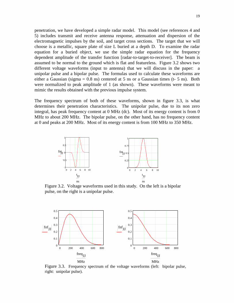
penetration, we have developed a simple radar model. This model (see references 4 and5) includes transmit and receive antenna response, attenuation and dispersion of theelectromagnetic impulses by the soil, and target cross sections. The target that we willchoose is a metallic, square plate of size L buried at a depth D. To examine the radarequation for a buried object, we use the simple radar equation for the frequencydependent amplitude of the transfer function [radar-to-target-to-receiver]. The beam isassumed to be normal to the ground which is flat and featureless. Figure 3.2 shows twodifferent voltage waveforms (input to antenna) that we will discuss in the paper: aunipolar pulse and a bipolar pulse. The formulas used to calculate these waveforms areeither a Gaussian (sigma = 0.8 ns) centered at 5 ns or a Gaussian times (t- 5 ns). Bothwere normalized to peak amplitude of 1 (as shown). These waveforms were meant tomimic the results obtained with the previous impulse system.
The frequency spectrum of both of these waveforms, shown in figure 3.3, is whatdetermines their penetration characteristics. The unipolar pulse, due to its non zerointegral, has peak frequency content at 0 MHz (dc). Most of its energy content is from 0MHz to about 200 MHz. The bipolar pulse, on the other hand, has no frequency contentat 0 and peaks at 200 MHz. Most of its energy content is from 100 MHz to 350 MHz.
0 2 4 6 8 101
0.5
0
0.5
1
fntJJ
tJJ
ns
0 2 4 6 8 100
0.25
0.5
0.75
1
fntJJ
tJJ
ns
Figure 3.2. Voltage waveforms used in this study. On the left is a bipolarpulse, on the right is a unipolar pulse.
0 200 400 600 8000
0.1
0.2
0.3
0.4
0.5
fnfJJ
freqJJ
MHz
0 200 400 600 8000
0.1
0.2
0.3
0.4
0.5
fnfJJ
freqJJ
MHzFigure 3.3. Frequency spectrum of the voltage waveforms (left: bipolar pulse,right: unipolar pulse).

20
0 100 200 300 4000
0.5
1
1.5
2
2.5
3
TFPJJ
freqJJ
MHz
0 200 400 600 800 10001
2
3
4
5
6
7
logσJJ
m2
freqJJ
MHz
Figure 3.4. Antenna transfer function (left) and the cross section of a flat metalplate with dimensions of 10 m by 10 m.
An existing antenna which may be used for this work is a large TEM horn with flaredaperture plates and a high-voltage inline coaxial ‘zipper’ balun as the input section. It hasa transfer function as shown in figure 3.4. This was developed by measuring two timedomain waveforms. One was a bipolar voltage pulse created by a custom pulse generatorwith a +/- 100 V amplitude, and primary spectral content from 50 to 400 MHz. The otherwas the main radiated E-field, at a range of 8.0 m. The transfer function was then formedby the complex ratio of the discrete Fourier transform of the radiated field divided by thetransform of the input excitation voltage. The cross section (in Air) of the target(a metalplate 10 m by 10 m) also increases with frequency (see figure 3.4). Because the antennatransfer function and the target cross section are larger at higher frequencies, the unipolarpulse will have less efficiency than the bipolar pulse. It is tempting to use waveforms thathave very high frequency components. On the other hand, the attenuation by the soil islarger at higher frequencies. Figure 3.5 shows attenuation for dry sand and San AntonioClay Loam with a water content of 5%.
10 100 1 1031.2
0.9
0.6
0.3
0
loga ,JJ 2
freqJJ
MHz
10 100 1 10340
30
20
10
0
loga ,JJ 3
freqJJ
MHz
Figure 3.5. The log of the attenuation versus frequency for a penetrationdepth of 10 m for dry sand (left) and San Antonio clay loam, 5% water(right).
21
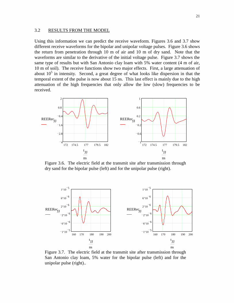
3.2 RESULTS FROM THE MODEL
Using this information we can predict the receive waveform. Figures 3.6 and 3.7 showdifferent receive waveforms for the bipolar and unipolar voltage pulses. Figure 3.6 showsthe return from penetration through 10 m of air and 10 m of dry sand. Note that thewaveforms are similar to the derivative of the initial voltage pulse. Figure 3.7 shows thesame type of results but with San Antonio clay loam with 5% water content (4 m of air,10 m of soil). The receive functions show two major effects. First, a large attenuation ofabout 105 in intensity. Second, a great degree of what looks like dispersion in that thetemporal extent of the pulse is now about 15 ns. This last effect is mainly due to the highattenuation of the high frequencies that only allow the low (slow) frequencies to bereceived.
172 174.5 177 179.5 1824
2.8
1.6
0.4
0.8
2
REERecJJ
tJJ
ns
172 174.5 177 179.5 1821
0.6
0.2
0.2
0.6
1
REERecJJ
tJJ
ns
Figure 3.6. The electric field at the transmit site after transmission throughdry sand for the bipolar pulse (left) and for the unipolar pulse (right).
160 170 180 190 2001 10
5
6 106
2 106
2 106
6 106
1 105
REERecJJ
tJJ
ns
160 170 180 190 2001 10
5
6 106
2 106
2 106
6 106
1 105
REERecJJ
tJJ
ns
Figure 3.7. The electric field at the transmit site after transmission throughSan Antonio clay loam, 5% water for the bipolar pulse (left) and for theunipolar pulse (right)..
22
4.0 RADAR TRANSMITTER
A radar transmitter is composed of a modulator that charges a pulse forming line, a pulseforming line that shapes (with the help of switches) the input pulse to an antenna, and theantenna. This chapter describes these three aspects of the radar transmitter we developedand also includes a section on the laser diode/ laser diode drivers we used.
4.1 MODULATOR
Two modulators were designed, built and tested: one was an all solid state, SCR-basedsystem and the other was a thyratron-based system. The SCR-based system wasdeveloped first because of our desire for an all solid state transmitter. The schematic forthe SCR modulator is shown in figure 4.1. The low voltage side of the transformer is aresonantly charged, SCR-based circuit capable of 1 kV output. The transformer had a150 to 1 turns ratio and was counter-wound. Thus, the voltage on the secondary is of thesame polarity as the voltage in the primary. The output of the transformer is connected tothe transmission line or pulse forming line using a stack of isolation diodes and a resistor.The need for the diodes, explained in detail in section 2.5, is to improve switch longevityby reducing long duration currents through the switch. Because of the electrical noiseproduced by the modulator, the modulator was housed in a sealed box with only thetransformer, isolation diode stack, and charge resistors outside of the box. We also builta battery-powered AC supply to run the modulator which was used for testing outdoors.Figure 4.2 is a photograph of the system with the SCR-based modulator prior toinstallation in the sealed box.
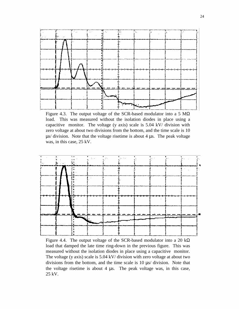
Figure 4.3 shows the output voltage from the SCR-based modulator into a 5 MΩ load.This was measured without the isolation diodes in place using a capacitive monitor. Thevoltage (y axis) scale is 5.04 kV/ division and the time scale is 10 µs/ division. Thevoltage risetime is about 4 µs. The peak voltage was, in this case, 25 kV. The waveformshows a positive pulse with a duration of ~30 µs which is followed by a negative pulse(peak negative voltage of -9 kV)with a duration of ~70 µs. Because of the need to avoidlong duration currents through the switch, we damped the output of the transformer usinga 20 kΩ load across the transmission line. The resulting voltage waveform is shown infigure 4.4. This waveform only has a~10 µs duration positive pulse and a damped (peaknegative voltage of -4 kV) negative pulse.
The SCR-based modulator was tested in this configuration to a peak voltage of ~80 kVand a repetition rate of 200 Hz.
The SCR-based modulator was connected to the transmission line, and the linedischarged with high gain GaAs switches. First, we tested the system in a unipolarconfiguration and obtained the appropriate output from the pulse forming line. We thenattempted to trigger two switches simultaneously but only one or the other would triggerproducing unipolar pulses instead of the desired bipolar pulse. This problem was

23
resolved, eventually, after much experimentation and testing. One of these tests was todevelop a modulator that would charge the line with faster risetime. It was erroneouslythought, based partly on previous results, that a faster risetime would result in smallerswitch jitter.
Figure 4.1. Schematic of the SCR-based modulator.
Figure 4.2. Photograph of the system SCR-based modulator prior toinstallation in the sealed box. The pulse forming line is in the horizontally-aligned tee at the left of the photograph, the transformer is in the verticalcontainer at the center, and the lower voltage circuitry of the modulator is tothe right. The large heat sink for the SCR is just to the right of thetransformer housing.
24
Figure 4.3. The output voltage of the SCR-based modulator into a 5 MΩload. This was measured without the isolation diodes in place using acapacitive monitor. The voltage (y axis) scale is 5.04 kV/ division withzero voltage at about two divisions from the bottom, and the time scale is 10µs/ division. Note that the voltage risetime is about 4 µs. The peak voltagewas, in this case, 25 kV.
Figure 4.4. The output voltage of the SCR-based modulator into a 20 kΩload that damped the late time ring-down in the previous figure. This wasmeasured without the isolation diodes in place using a capacitive monitor.The voltage (y axis) scale is 5.04 kV/ division with zero voltage at about twodivisions from the bottom, and the time scale is 10 µs/ division. Note thatthe voltage risetime is about 4 µs. The peak voltage was, in this case,25 kV.
25
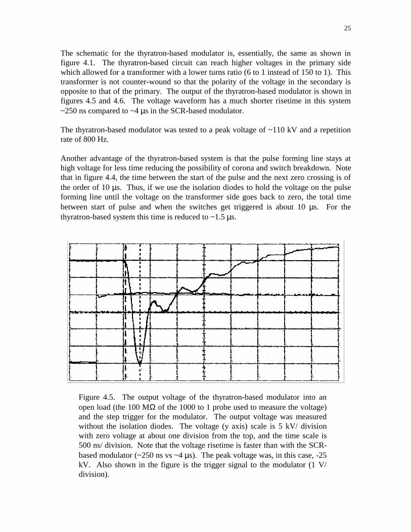
The schematic for the thyratron-based modulator is, essentially, the same as shown infigure 4.1. The thyratron-based circuit can reach higher voltages in the primary sidewhich allowed for a transformer with a lower turns ratio (6 to 1 instead of 150 to 1). Thistransformer is not counter-wound so that the polarity of the voltage in the secondary isopposite to that of the primary. The output of the thyratron-based modulator is shown infigures 4.5 and 4.6. The voltage waveform has a much shorter risetime in this system~250 ns compared to ~4 µs in the SCR-based modulator.
The thyratron-based modulator was tested to a peak voltage of ~110 kV and a repetitionrate of 800 Hz.
Another advantage of the thyratron-based system is that the pulse forming line stays athigh voltage for less time reducing the possibility of corona and switch breakdown. Notethat in figure 4.4, the time between the start of the pulse and the next zero crossing is ofthe order of 10 µs. Thus, if we use the isolation diodes to hold the voltage on the pulseforming line until the voltage on the transformer side goes back to zero, the total timebetween start of pulse and when the switches get triggered is about 10 µs. For thethyratron-based system this time is reduced to ~1.5 µs.
Figure 4.5. The output voltage of the thyratron-based modulator into anopen load (the 100 MΩ of the 1000 to 1 probe used to measure the voltage)and the step trigger for the modulator. The output voltage was measuredwithout the isolation diodes. The voltage (y axis) scale is 5 kV/ divisionwith zero voltage at about one division from the top, and the time scale is500 ns/ division. Note that the voltage risetime is faster than with the SCR-based modulator (~250 ns vs ~4 µs). The peak voltage was, in this case, -25kV. Also shown in the figure is the trigger signal to the modulator (1 V/division).

26
Figure 4.6. The output voltage of the thyratron-based modulator into a 5 kΩload that damped the late time voltage and the step trigger for the modulator.The output voltage was measured without the isolation diodes using a 1000to 1 probe. The voltage (y axis) scale is 5 kV/ division with zero voltage atabout two divisions from the top, and the time scale is 500 ns/ division.Note that the voltage risetime is ~320 ns. The peak voltage was, in thiscase, -25 kV. Also shown in the figure is the trigger signal to the modulator(1 V/ division).
4.2 PULSE FORMING LINE
A pulse forming line (PFL) which incorporates two PCSS and a capacitive voltage probewas designed and tested. A schematic of the system is shown in figure 3.1. The PFL ischarged by the modulator. If only switch 1 is triggered, the output pulse to the load is aunipolar pulse of the same polarity as the PFL. If both switches are triggered, the PFLproduces a bipolar pulse. Figures 4.7 and 4.8 show the PFL’s housing and the PFL itself.Note that the two switches are placed horizontally.
We developed several voltage monitors to measure the voltage on the pulse forming lineand on the feed to the antenna, the most complicated of which was an integratingcapacitive voltage probe. New laser diode array drivers were also built, assembled, andshielded since previous drivers were found to be too susceptible to electro-magneticinterference from the pulser/ transmitter and we needed to assure that the lasers were notbeing triggered by the modulator or by the first triggering or ringing in the pulse formingline. At one point, jitter in the system was due to false triggering of the lasers.
27
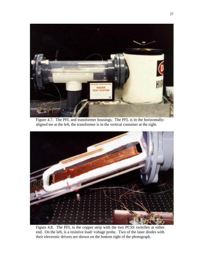
Figure 4.7. The PFL and transformer housings. The PFL is in the horizontally-aligned tee at the left, the transformer is in the vertical container at the right.
Figure 4.8. The PFL is the copper strip with the two PCSS switches at eitherend. On the left, is a resistive load/ voltage probe. Two of the laser diodes withtheir electronic drivers are shown on the bottom right of the photograph.
28
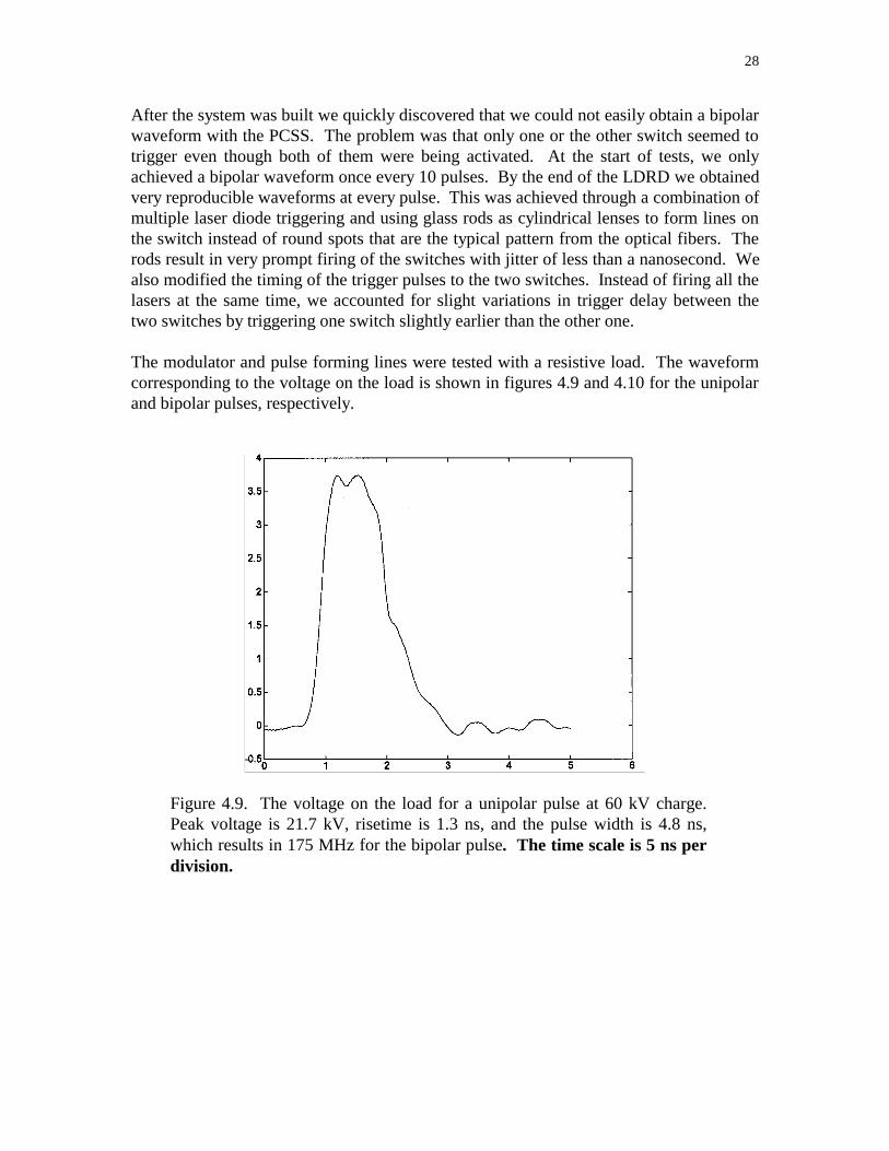
After the system was built we quickly discovered that we could not easily obtain a bipolarwaveform with the PCSS. The problem was that only one or the other switch seemed totrigger even though both of them were being activated. At the start of tests, we onlyachieved a bipolar waveform once every 10 pulses. By the end of the LDRD we obtainedvery reproducible waveforms at every pulse. This was achieved through a combination ofmultiple laser diode triggering and using glass rods as cylindrical lenses to form lines onthe switch instead of round spots that are the typical pattern from the optical fibers. Therods result in very prompt firing of the switches with jitter of less than a nanosecond. Wealso modified the timing of the trigger pulses to the two switches. Instead of firing all thelasers at the same time, we accounted for slight variations in trigger delay between thetwo switches by triggering one switch slightly earlier than the other one.
The modulator and pulse forming lines were tested with a resistive load. The waveformcorresponding to the voltage on the load is shown in figures 4.9 and 4.10 for the unipolarand bipolar pulses, respectively.
Figure 4.9. The voltage on the load for a unipolar pulse at 60 kV charge.Peak voltage is 21.7 kV, risetime is 1.3 ns, and the pulse width is 4.8 ns,which results in 175 MHz for the bipolar pulse. The time scale is 5 ns perdivision.
29
Figure 4.10. The voltage on the load for a bipolar pulse at 75 kV charge.Peak voltage is 31.2 kV, risetime is 113 ns, and the full width of the first(positive) pulse is 3.8 ns. A single cycle with a period of 7.6 ns has a centerfrequency of 110 MHz. The time scale has a total span of 50 ns.
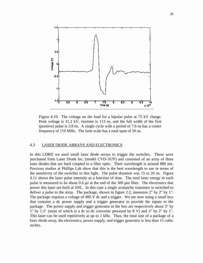
4.3 LASER DIODE ARRAYS AND ELECTRONICS
In this LDRD we used small laser diode arrays to trigger the switches. These werepurchased from Laser Diode Inc. (model CVD-167F) and consisted of an array of threelaser diodes that are hard coupled to a fiber optic. Their wavelength is around 880 nm.Previous studies at Phillips Lab show that this is the best wavelength to use in terms ofthe sensitivity of the switches to this light. The pulse duration was 15 to 20 ns. Figure4.11 shows the laser pulse intensity as a function of time. The total laser energy in eachpulse is measured to be about 0.6 µJ at the end of the 300 µm fiber. The electronics thatpower this laser are built at SNL. In this case a single avalanche transistor is switched todeliver a pulse to the array. The package, shown in figure 2.2, measures 2" by 2" by 1".The package requires a voltage of 400 V dc and a trigger. We are now using a small boxthat contains a dc power supply and a trigger generator to provide the inputs to thepackage. The power supply and trigger generator in the box are respectively about 3" by1" by 1.5" (most of which is a dc to dc converter powered by 8 V) and 3" by 2" by 1".This laser can be used repetitively at up to 1 kHz. Thus, the total size of a package of alaser diode array, the electronics, power supply, and trigger generator is less than 15 cubicinches.
30
0 0.2 0.4 0.6 0.8 1 1.2
x 10-7
-0.1
0
0.1
0.2
0.3
0.4
0.5
0.6
0.7
0.8
0.9
Figure 4.11. The output of the laser diode array. The risetime in thisparticular waveform is 5 ns and the full width at half maximum is 13 ns.This laser diode array operated at 885 nm and had an output energy (fromthe fiber) of 0.58 µJ.
4.4 ANTENNA AND IMPEDANCE MATCHING SECTION
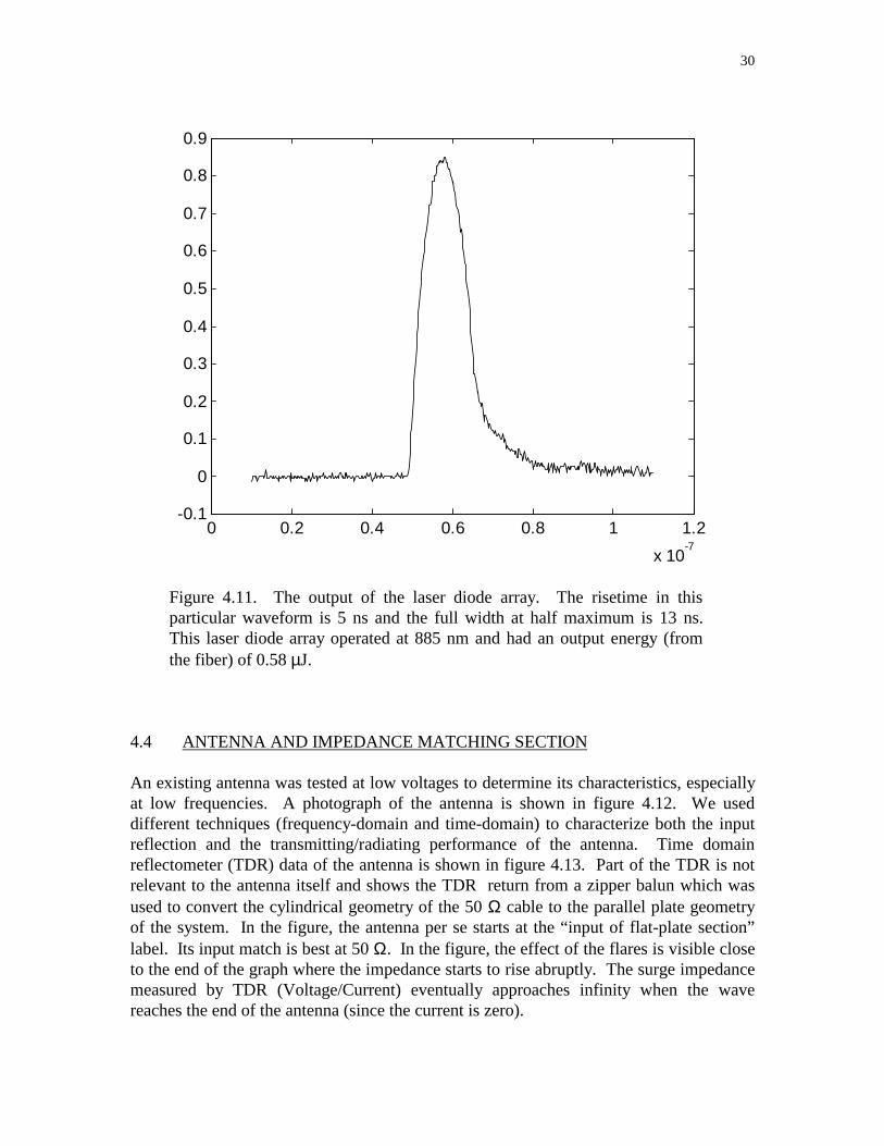
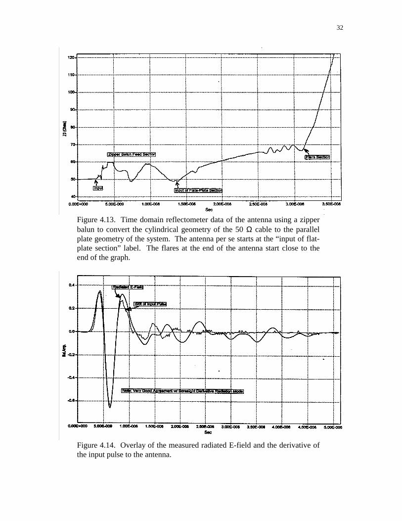
An existing antenna was tested at low voltages to determine its characteristics, especiallyat low frequencies. A photograph of the antenna is shown in figure 4.12. We useddifferent techniques (frequency-domain and time-domain) to characterize both the inputreflection and the transmitting/radiating performance of the antenna. Time domainreflectometer (TDR) data of the antenna is shown in figure 4.13. Part of the TDR is notrelevant to the antenna itself and shows the TDR return from a zipper balun which wasused to convert the cylindrical geometry of the 50 Ω cable to the parallel plate geometryof the system. In the figure, the antenna per se starts at the “input of flat-plate section”label. Its input match is best at 50 Ω. In the figure, the effect of the flares is visible closeto the end of the graph where the impedance starts to rise abruptly. The surge impedancemeasured by TDR (Voltage/Current) eventually approaches infinity when the wavereaches the end of the antenna (since the current is zero).

31
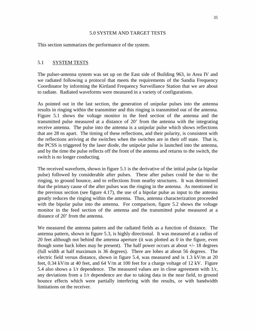
The transfer function of the antenna was shown in figure 3.4 and discussed in thatchapter. The transfer function has a low frequency roll-off of about 70 MHz (meaningthat the antenna does not radiate effectively below 70 MHz). The antenna acts as aderivative antenna almost exclusively. Figure 4.14 shows a comparison of a radiated E-field and the derivative of the input to the antenna. Because of these low voltage tests, wemodified the design of the pulse forming line to have 50 Ω impedance and for it toproduce a bipolar pulse with a 5 ns period (so that its peak spectral content is at 200 MHz(the frequency roll-off). We also built and calibrated a voltage divider to measure thevoltage in the antenna (at the feed point).
Figure 4.12. The antenna. For scale, note the door behind the antenna.
32
Figure 4.13. Time domain reflectometer data of the antenna using a zipperbalun to convert the cylindrical geometry of the 50 Ω cable to the parallelplate geometry of the system. The antenna per se starts at the “input of flat-plate section” label. The flares at the end of the antenna start close to theend of the graph.
Figure 4.14. Overlay of the measured radiated E-field and the derivative ofthe input pulse to the antenna.

33
The receive antenna is a crucial part of this LDRD. Making measurements of antennaresponse characteristics in the VHF range is well known to be a difficult task. We testeda D-dot antenna and a resistively-loaded TEM horn as receive antennas. The D-dotantenna has good frequency response that extends to very low frequencies but it lackedsensitivity and, thus, the data was too noisy. An alternative was to use the previouslycalibrated TEM horn. This antenna was built for transient/ time-domain receivingapplications such as this one prior to this LDRD. It was designed to produce an outputvoltage proportional to the incident field. It has a very low dispersion design, discreteresistor loading of the aperture to reduce late- time undershoot of the receiving impulseresponse, and a broadband matching section. It was calibrated by comparing its outputwith a precision D-dot receiving antenna (at Sandia) and using a time- domain monocone/ground plane antenna range (at NIST by Dr. A. Ondrejka). It was designed to have abandwidth of roughly 100 MHz to 7 GHz, but has an upper roll-off (-3 dB) frequency ofonly 2.75 GHz (adequate for these experiments). The pass-band of the receiving antennahas an effective height of 2.0 cm averaged over the ~75 MHz to 2 GHz range.Unfortunately, these calibration procedures were carried out at facilities which did notprovide the most desirable information in the operating band of the pulser. Regardless,the low frequency roll-off of this antenna (75 MHz) is not as low as we would like (30MHz). Given that the low frequency roll-off of the transmit antenna is 70 MHz, the roll-off of the receive antenna is barely acceptable.
Once the modulator, pulse forming line and antenna were built and tested individually,the system was assembled and tested as a transmitter. At this time we observed that thesystem was producing late time ringing: the initial pulse that was sent from the pulseforming line to the antenna was not radiated in its entirety and part of it was reflectedback to the pulse forming line and eventually radiated at late times. Figure 4.15 showsthe ringing as measured by the voltage monitor at the feed of the antenna. These laterpulses are a problem when the receiver is placed adjacent to the antenna since the pulsethat arrives from the target may be coincident in time with the late time ringing and maybe masked by it. The main reason for the ringing is due to frequency mismatch betweenthe pulser (in the unipolar configuration) and the antenna. The unipolar waveform haspeak frequency content at 0 Hz and the antenna is not an effective transmitter atfrequencies below 70 MHz. Thus we expected to see ringing in the pulser-antennasystem, but it did not necessarily have to be radiated. The radiated waveform shows thatthis ringing does result in a transmitted pulse with after pulses that last about 200 ns (seesection 5). We reduced this late time ringing in two different ways. As demonstrated infigure 4.15, one way was to use the bipolar waveform instead of the unipolar pulse due toa better match with the antenna of the former due to its higher frequency content.

34
Figure 4.15. The voltage measured at the feed of the antenna for threedifferent PFL output pulses: a positive unipolar pulse (solid line), a negativeunipolar pulse (dotted line), and a bipolar pulse (dash-dot line). Note thatboth unipolar pulses show a second pulse about 25 ns from the initial pulse.This ringing is due to the pulse reaching the antenna opening and reflectingback to the monitor.
We also reduced the ringing in the antenna by using an impedance matching section toconnect the pulse forming line to the antenna. The PFL ends with two copper strips of1.5” width separated by 1/2” Lexan. This was connected to the start of the antenna whichwas also at 50 Ω but in air resulting in two plates that were 3” wide separated by 1/2” ofair. It was felt that the abrupt change in width was not desirable, thus the impedancematching section was made with a gradual change in the width by tapering the amount ofLexan between the plates. This matching section was adjusted by using TDR data toobtain 50 Ω impedance throughout the transition.
35
5.0 SYSTEM AND TARGET TESTS
This section summarizes the performance of the system.
5.1 SYSTEM TESTS
The pulser-antenna system was set up on the East side of Building 963, in Area IV andwe radiated following a protocol that meets the requirements of the Sandia FrequencyCoordinator by informing the Kirtland Frequency Surveillance Station that we are aboutto radiate. Radiated waveforms were measured in a variety of configurations.
As pointed out in the last section, the generation of unipolar pulses into the antennaresults in ringing within the transmitter and this ringing is transmitted out of the antenna.Figure 5.1 shows the voltage monitor in the feed section of the antenna and thetransmitted pulse measured at a distance of 20’ from the antenna with the integratingreceive antenna. The pulse into the antenna is a unipolar pulse which shows reflectionsthat are 28 ns apart. The timing of these reflections, and their polarity, is consistent withthe reflections arriving at the switches when the switches are in their off state. That is,the PCSS is triggered by the laser diode, the unipolar pulse is launched into the antenna,and by the time the pulse reflects off the front of the antenna and returns to the switch, theswitch is no longer conducting.
The received waveform, shown in figure 5.1 is the derivative of the initial pulse (a bipolarpulse) followed by considerable after pulses. These after pulses could be due to theringing, to ground bounce, and to reflections from nearby structures. It was determinedthat the primary cause of the after pulses was the ringing in the antenna. As mentioned inthe previous section (see figure 4.17), the use of a bipolar pulse as input to the antennagreatly reduces the ringing within the antenna. Thus, antenna characterization proceededwith the bipolar pulse into the antenna. For comparison, figure 5.2 shows the voltagemonitor in the feed section of the antenna and the transmitted pulse measured at adistance of 20’ from the antenna.
We measured the antenna pattern and the radiated fields as a function of distance. Theantenna pattern, shown in figure 5.3, is highly directional. It was measured at a radius of20 feet although not behind the antenna aperture (it was plotted as 0 in the figure, eventhough some back lobes may be present). The half power occurs at about +/- 18 degrees(full width at half maximum is 36 degrees). There are lobes at about 56 degrees. Theelectric field versus distance, shown in figure 5.4, was measured and is 1.3 kV/m at 20feet, 0.34 kV/m at 40 feet, and 64 V/m at 100 feet for a charge voltage of 12 kV. Figure5.4 also shows a 1/r dependence. The measured values are in close agreement with 1/r,any deviations from a 1/r dependence are due to taking data in the near field, to groundbounce effects which were partially interfering with the results, or with bandwidthlimitations on the receiver.

36
Figure 5.1. This figure shows two waveforms. The first one is the pulseinto the antenna, a unipolar pulse. Note that the transmitter rings with aperiod of about 28 ns. The second waveform is the receive signal atboresight (20’ distance) and shows the effect of this ringing.
0 20 40 60 80 100 120-2
-1.5
-1
-0.5
0
0.5
1
1.5
2
2.5
Time(ns)
Raw
Sig
nal V
olta
ge
GPR -- Antenna Input and Receive Pulse
Figure 5.2. This figure shows two waveforms. The first one is the pulseinto the antenna, a bipolar pulse. Note that the ringing of the transmitter ismuch reduced when compared to that of the unipolar pulse. The secondwaveform is the receive signal at boresight (20’ distance).

37
011.25
22.533.75
45
56.25
67.5
78.75
90
101.25
112.5
123.75
135
146.25157.5
168.75180
191.25202.5
213.75
225
236.25
247.5
258.75
270
281.25
292.5
303.75
315
326.25337.5
348.75
Figure 5.3. Two curves showing the antenna power pattern (the power wasnot measured behind the antenna aperture and is plotted as 0). One of thecurves is shown expanded by a factor of 6 to highlight the lobes at 56°.
0
500
1000
1500
2000
2500
3000
3500
0 10 20 30 40 50 60 70 80 90 100
Figure 5.4. Electric field in V/m () as function of distance from theantenna aperture for a charge voltage of 12 kV. A plot of 1/distance,normalized at 40 feet is also included ().

38
5.2 TESTS WITH UN-OBSCURED TARGETS
After the system was characterized, we measured the return waveform from a target inair: We measured return waveforms from a 4’ by 8’ metal plate. The best results wereobtained with the plate at 45° relative to the direction of the incoming electromagneticwave and the receiver at 90 degrees. This reduced the effects of antenna ringing relativeto the case when the receiver was co-located with the transmit antenna. The target was ata distance of ~20’ from the antenna (boresight) and the receiver at ~20’ from the target.Figure 5.5 shows the voltage input to the antenna and the receive (reflected) signal. Incomparison to figures 5.1 and 5.2 the big difference is that the first signals that arrive atthe receiver are not the boresight signals. There is a weaker signal that is transmitted at45° and arrives at the receiver prior to the signal that is reflected off the target.
0 20 40 60 80 100 120-5
-4
-3
-2
-1
0
1
2
Time(ns)
Raw
Sig
nal V
olta
ge
GPR -- Antenna Input and Received (Reflected) Pulse
Figure 5.5. This figure shows two waveforms. The first one is the pulseinto the antenna, a bipolar pulse. The second waveform is the receive signalfrom a 4’ by 8’ metal plate. The target was ~20’ from the antenna, inclinedat 45° from boresight, so that the reflected wave was aimed at the receiver.
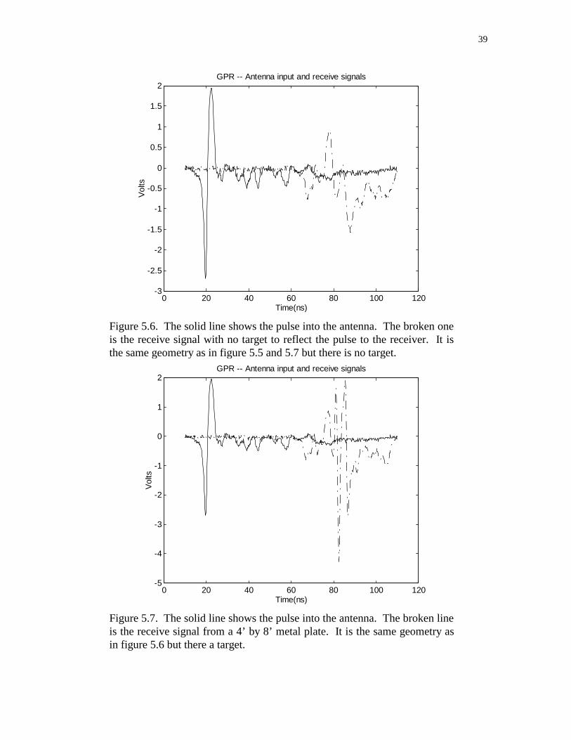
A better demonstration of the ability of the system to observe targets is to use backgroundsubtraction. Figure 5.6 shows the received signal with no target. The only signalsreceived are 45° emission from the antenna and reflections from nearby objects. Figure5.7 shows the signal with the target. Figure 5.8 shows the subtraction of the two signals.
39
0 20 40 60 80 100 120-3
-2.5
-2
-1.5
-1
-0.5
0
0.5
1
1.5
2
Time(ns)
Vol
ts
GPR -- Antenna input and receive signals
Figure 5.6. The solid line shows the pulse into the antenna. The broken oneis the receive signal with no target to reflect the pulse to the receiver. It isthe same geometry as in figure 5.5 and 5.7 but there is no target.
0 20 40 60 80 100 120-5
-4
-3
-2
-1
0
1
2
Time(ns)
Vol
ts
GPR -- Antenna input and receive signals
Figure 5.7. The solid line shows the pulse into the antenna. The broken lineis the receive signal from a 4’ by 8’ metal plate. It is the same geometry asin figure 5.6 but there a target.

40
0 20 40 60 80 100 120-4
-3
-2
-1
0
1
2
3
Time(ns)
Re
ceiv
e S
igna
l(vo
lts)
GPR Receive Data
Figure 5.8. The difference in the received waveforms with and without atarget.
70 75 80 85 90 95 100
-3
-2
-1
0
1
2
Time(ns)
Re
ceiv
e S
igna
l(vo
lts)
GPR Receive Data
Figure 5.9. The difference in the received waveforms with and without atarget in an expanded time scale.

41
5.3 PENETRATION THROUGH CONCRETE
We measured penetration through concrete, and return waveforms from targets behindconcrete walls. First, we placed a receiver behind large concrete blocks used for radiationshielding: each block is 3' by 2' by 6' . We used a total of 6 blocks and a metal plate ontop to reduce the effect of the wave that travels around the blocks. Figure 5.10 shows thesetup. The blocks were at 100’ from the antenna. The signal was measured with thereceiver inside the block structure and just outside. Figures 5.11 and 5.12 show thewaveforms. Note that the signal amplitude was reduced by a factor of only 2.8.
We also placed a 4’ by 8’ metal-plate target behind the wall of building 962 and measuredreturns. Measurable penetration signals were observed.
Finally, we placed the transmitter to look for penetration of real soil. We were not able tomeasure any returns due to two reasons. First, we used the transmit antenna as a receiveantenna. The problem with this configuration is that we had a low dynamic rangemeasurement since the monitor had to measure the high voltage pulse into the antenna.The second reason was that recent rains had raised the water content of the soil to 8%.
Figure 5.10. This photograph shows the concrete blocks used for tests ofpenetration through concrete. The blocks are those used for radiationshielding: 2’ thick by 3’ high by 6’ wide, made from high density concrete.The receiver was placed behind the blocks.

42
Figure 5.11 The waveform with the receiver to the side of the blocks.
Figure 5.12. The waveform with the receiver behind the blocks.

43
6.0 REFERENCES
1) For general references on high gain PCSS technology see the following:a.) IEEE Pulsed Power Conferences, 1985-97 (odd years)b.) IEEE Power Modulator Symposia, 1986-96 (even years)c.) SPIE Optically Activated Switching Conferences I-IV, 1990, 1992, 1993, 1994.d.) F. J. Zutavern, G. M. Loubriel, M. W. O'Malley, L. P. Schanwald, W. D.
Helgeson, D. L. McLaughlin, and B. B. McKenzie, "Photoconductivesemiconductor switch experiments for pulsed power applications," IEEE Trans.Elect. Devices, Vol. 37, No. 12, 1990, pp. 2472-2477.
e.) A. Rosen and F. J. Zutavern, Eds., High-Power Optically Activated Solid StateSwitches, Artech House, Boston, 1993, pp. 245-296.
f.) G. M. Loubriel, F. J. Zutavern, H. P. Hjalmarson, R. R. Gallegos, W. D.Helgeson, and M. W. O'Malley, "Measurement of the Velocity of CurrentFilaments in Optically Triggered, High Gain GaAs Switches", Applied PhysicsLetters, Vol. 64, No. 24, 13 June, 1994, pp. 3323-3325.
g.) G. M. Loubriel, F. J. Zutavern, A. G. Baca, H. P. Hjalmarson, T. A. Plut, W. D.Helgeson, M. W. O'Malley, M. H. Ruebush, and D. J. Brown, "PhotoconductiveSemiconductor Switches," IEEE Transactions on Plasma Science, 25, 1997, pp.124-130.
2) References on switch longevity:a) G. M. Loubriel, F. J. Zutavern, A. Mar, M. W. O’Malley, W. D. Helgeson, D. J.
Brown, H. P. Hjalmarson, and A. G. Baca, “Longevity of Optically Activated,High Gain GaAs Photoconductive Semiconductor Switches,” to be published inProceedings of 11th IEEE Pulsed Power Conference, Baltimore, MD, June 29-July 2, 1997.
b) G. M. Loubriel, F. J. Zutavern, A. Mar, H. P. Hjalmarson, A. G. Baca, M. W.O’Malley, W. D. Helgeson, D. J. Brown, and R. A. Falk, “Longevity ofOptically Activated, High Gain GaAs Photoconductive SemiconductorSwitches,” to be published in IEEE Transactions on Plasma Science.
3) G. M. Loubriel, et al, "High Gain GaAs Photoconductive Semiconductor Switches forImpulse Sources," Proc. of SPIE Optically Activated Switching Conference IV,SPIE Vol. 2343, p. 180, W. R. Donaldson, ed., Boston, MA, 1994.
4) G. M. Loubriel, M. T. Buttram, J. F. Aurand, and F. J. Zutavern, "Ground PenetratingRadar Enabled by High Gain GaAs Photoconductive Semiconductor Switches,"in Ultra-Wideband, Short Pulse Electromagnetics 3, A. Stone, C. Baum, and L.Carin, eds., Plenum Press, NY, 1996, pp. 17- 24.
5) G. M. Loubriel, F. J. Zutavern, W. D. Helgeson, D. J. Brown, and M. W. O’Malley,“High Gain GaAs Switches for Ground Penetrating Radar”, Proc. 22nd PowerModulator Symposium (IEEE, NY, 1996), Boca Raton, FL, June 24-27, 1996,pp. 165-168.

44
DISTRIBUTIONINTERNAL DISTRIBUTION
1314, MS 1060 A. G. Baca1314, MS 0603 T. E. Zipperian2674, MS 0328 J. A. Wilder2674, MS 0328 S. C. Holswade7585, MS 1148 F. L. Peace9000, MS 0151 G. Yonas9232, MS 0820 H. P. Hjalmarson9300, MS 1165 J. Polito9301, MS 1165 D. M. Rondeau9331, MS 1153 D. W. Brown9331, MS 1153 M. T. Buttram9331, MS 1153 W. D. Helgeson9331, MS 1153 G. M. Loubriel9331, MS 1153 A. Mar9331, MS 1153 M. W. O'Malley9331, MS 1153 F. J. Zutavern9500, MS 1190 D. L. Cook9512, MS 1188 R. A. Hamil4916, MS 0899 Technical Library (5)8940-2, MS 9018 Central Technical Files12690, MS 0619 Document Processing for DOE/OSTI (2)