electronic design project report yusof
TRANSCRIPT

7/27/2019 Electronic Design Project Report Yusof
http://slidepdf.com/reader/full/electronic-design-project-report-yusof 1/17

7/27/2019 Electronic Design Project Report Yusof
http://slidepdf.com/reader/full/electronic-design-project-report-yusof 2/17
If the product requirement doesn’t achieve the client’s expectation, the company will get heavy
penalty for the failures.
Objective
Objective of this project is :
To use and apply the studying of PCB in working environment
To dedicate self to the electronic design work, and to know how the components and design
related to electronics.
To learn how to use Protheus.7, including the uses of ISIS and ARES.
To learnt how a PCB is created step by step including designing, printing, drilling, etching etc. To study about the devices used to complete the design of the board.
To observe the result of the LED output happened after the finished of the project.
Aim
To create an easy to understand circuit board kit that can be understand for student
especially. The minor target is to sell the product to the market and learnt to fulfil the
client’s requirement, if it is not burden the company and making loses that the company has
to take if the client rejected the product. In order to fulfil all the situated requirement, truth
table, early designing should be done to encounter major and minor problem in the future.
Example of a battery car tester

7/27/2019 Electronic Design Project Report Yusof
http://slidepdf.com/reader/full/electronic-design-project-report-yusof 3/17
Block diagram
Equipment and components
Equipment and components are the major parts that consist in this project. In this
project, we did use our own lab in Unikl MFI, as all the equipment are available and can be
used, including designing(Protheus.7), printing, drilling, UV laminating, etching and so on.
Equipment.
Computer that is used to monitored ISIS and ARES. This is important in designing part.

7/27/2019 Electronic Design Project Report Yusof
http://slidepdf.com/reader/full/electronic-design-project-report-yusof 4/17
Printer to print out the component’s part and solder point.
The Semi- automatic PCB CNC drilling machine.
This is use to drill the point-to-drill of the PCB board.
It is easier to use fully automatic CNC drill, but we used
Semi auto in our lab.
Photonex UV laminating.

7/27/2019 Electronic Design Project Report Yusof
http://slidepdf.com/reader/full/electronic-design-project-report-yusof 5/17
UV explousere.
Tri-Tank etching/stripping
Components.
The components or devices that been used in this project is OP AMP, resistor, LED, battety,
voltmeter, capacitor, oscilloscope.
All the components above are parts in the ISIS.

7/27/2019 Electronic Design Project Report Yusof
http://slidepdf.com/reader/full/electronic-design-project-report-yusof 6/17
Project Hypothesis
Level Of Voltage L.E.DRed Yellow Green
X < 9V 9.5V < X < 11V 11V < Z < 13V
X > 13V
This is the truth table of the incoming result. The result should be like this. If the battery
voltage is below 9V, all LED will be off, and vice versa to the 13V and above battery voltage.
Methodology
I. First, design the circuit diagram in the ISIS.
II. Convert the circuit into ARES.
III. Print out the component parts.
IV. Transfer the folder into CNC drilling computer.
V. Using ISO CAM, drill the set the drill, drill point and so on.
VI. Place the board into the CNC drill.
VII. Laminate the PCB using blue UV plastic.
VIII. Soak the PCB using Sodium Hydroxide and Sodium Carbonate, by using Stripper and
Developer tank.
IX. Laminate again using green UV plastic.
X. Solder all components to the PCB board.

7/27/2019 Electronic Design Project Report Yusof
http://slidepdf.com/reader/full/electronic-design-project-report-yusof 7/17
Calculation

7/27/2019 Electronic Design Project Report Yusof
http://slidepdf.com/reader/full/electronic-design-project-report-yusof 8/17
Flowchart
STARTDesign circuit using ISIS
softwareConvert the circuit to ARES
Print out the component
part and solder resist
Soak PCB into the tri tank to
remove all the unwanted
film
Solder all the component
into PCB
Drill the point on PCB board
using CNC machine.
Laminate the PCB using UV
laminating strip.
END

7/27/2019 Electronic Design Project Report Yusof
http://slidepdf.com/reader/full/electronic-design-project-report-yusof 9/17
Procedure
Below are the picture of an example ISIS design :-
Using Protheus7.0, enter ISIS and insert the device and components needed. The device that
should inserted into the plane are : -
- Battery (amplitude 9.5V and varies). Using DC voltage source.
- CONN-SIL2 ( Connector strip )
- Red LED
- Green LED
- Yellow LED
- LM741 ( Operational Amplifier )
- MINRES10K ( Resistor : the value can change by double click the description of the
resistor in the plane )
7/27/2019 Electronic Design Project Report Yusof
http://slidepdf.com/reader/full/electronic-design-project-report-yusof 10/17
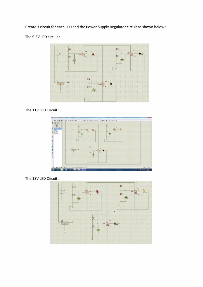
Create 3 circuit for each LED and the Power Supply Regulator circuit as shown below : -
The 9.5V LED circuit :
The 11V LED Circuit :
The 13V LED Circuit :

7/27/2019 Electronic Design Project Report Yusof
http://slidepdf.com/reader/full/electronic-design-project-report-yusof 11/17
0V LED circuit :
After done create all the circuit in the plane, transfer the circuit to the ARES PCB LAYOUT by
include all the components by click the “ARES” icon.
The circuit figure after transfer to the ARES PCB LAYOUT and connect all the components : -
Print out three mask that will be used in the laminating process after this :-

7/27/2019 Electronic Design Project Report Yusof
http://slidepdf.com/reader/full/electronic-design-project-report-yusof 12/17
Below is the product after print the circuit layout by use the above setting for track mask : -
The track mask
Setting for label mask: -
Below is the output after print the circuit layout by use the above setting for label mask : -
The label mask

7/27/2019 Electronic Design Project Report Yusof
http://slidepdf.com/reader/full/electronic-design-project-report-yusof 13/17
Setting for dot mask: -
Below is the product after print the circuit layout by use the above setting for dot mask : -
The dot mask

7/27/2019 Electronic Design Project Report Yusof
http://slidepdf.com/reader/full/electronic-design-project-report-yusof 14/17
After done print all the mask layout, the next task is to create the components hole onto the
single layer board by using the PCB CNC machine that connect with the ISOCAM software in
the computer in the lab.
PCB CNC machine.
Below are the instruction for create the components hole onto the single layer board and
how to using the ISOCAM sofware : -
1) Open ARES
- Select PCB, mirror-X
- Select output
- Set output origin
- Click origin to set
- Select output
- CADCAM output, metric mm
2) Open ISOCAM
- Load file
- CADCAM drill
- Number format: 2 4
- Load file
- CADCAM bottom copper
- Number format: 2 4
- L0
- Save
- Format: 2 3
- Option :
Include drill tool in drill file
- Drill filename :
( create new file name – no need .nc )
- OK
3) Open RouterPRO
-
Drill file
>>

7/27/2019 Electronic Design Project Report Yusof
http://slidepdf.com/reader/full/electronic-design-project-report-yusof 15/17
7/27/2019 Electronic Design Project Report Yusof
http://slidepdf.com/reader/full/electronic-design-project-report-yusof 16/17
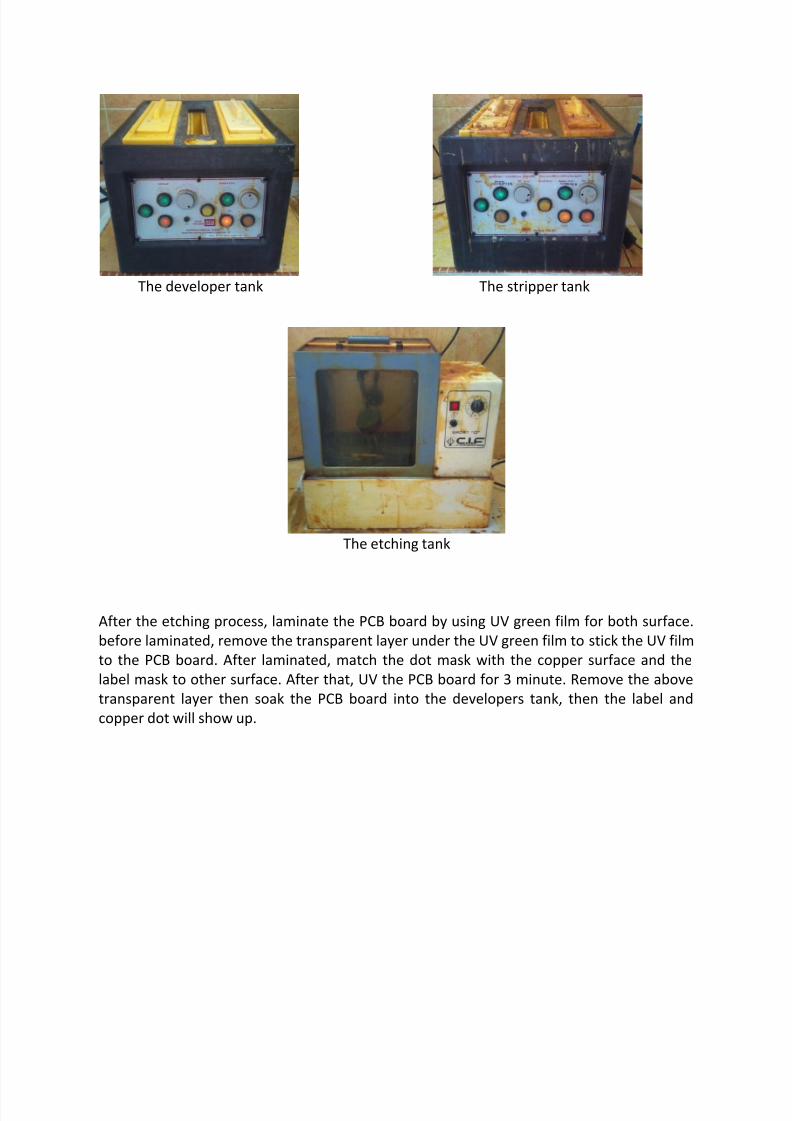
The developer tank The stripper tank
The etching tank
After the etching process, laminate the PCB board by using UV green film for both surface.
before laminated, remove the transparent layer under the UV green film to stick the UV film
to the PCB board. After laminated, match the dot mask with the copper surface and the
label mask to other surface. After that, UV the PCB board for 3 minute. Remove the above
transparent layer then soak the PCB board into the developers tank, then the label and
copper dot will show up.

7/27/2019 Electronic Design Project Report Yusof
http://slidepdf.com/reader/full/electronic-design-project-report-yusof 17/17
Conclusion
The conclusion from this project that we can learn is how we study the electronicdesign of a battery car tester. The design is fairly simple and can be used in workshop or so
whatever. The main objective of this project is to make us study how the digital electronic of
a PCB work. We did realise that the PCB is really reliable and can be used in many other
electronic design, except that it may varies in their shape and size. The size, the material,
and the shape of the PCB is part of the designer to do and to arrange the component in his
or her own form. And what we can conclude else is, if we been given a task or job, do it
quickly without procrastinate. This can be shown if a client give us some requirement or job,
we need to do it in his specify or the company should pay for what wrong we did.
In learning progress, we did learnt on how device, equipment work to regulate some
process. We learnt on how device work, components characteristic. For an example the UV
strip that cannot be put under sunlight, though it do make it unusedable. Our flow of work
did show us on how to manage simple task by doing work step by step. We should prepare
our work, do some calculation first, and do some research before conduct the project. This
is to prevent some loses or miscalculation that may lead the unworthy cost to be involve.