board examinations nov-2019 answer key qpcode-207 … · ii gate array based asics a. channeled...
TRANSCRIPT
1
BOARD EXAMINATIONS –NOV-2019
ANSWER KEY
QPCODE-207
34053- VERY LARGE SCALE INTEGRATION
2
PART – A [Each Answers Carried 2 Marks]
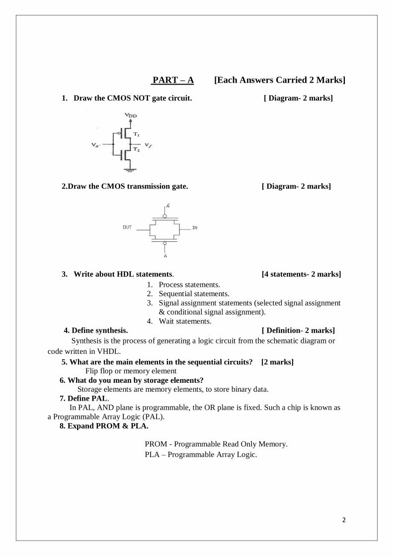
1. Draw the CMOS NOT gate circuit. [ Diagram- 2 marks]
2.Draw the CMOS transmission gate. [ Diagram- 2 marks]
3. Write about HDL statements. [4 statements- 2 marks]
1. Process statements.
2. Sequential statements.
3. Signal assignment statements (selected signal assignment
& conditional signal assignment).
4. Wait statements.
4. Define synthesis. [ Definition- 2 marks]
Synthesis is the process of generating a logic circuit from the schematic diagram or
code written in VHDL.
5. What are the main elements in the sequential circuits? [2 marks]
Flip flop or memory element
6. What do you mean by storage elements?
Storage elements are memory elements, to store binary data.
7. Define PAL.
In PAL, AND plane is programmable, the OR plane is fixed. Such a chip is known as
a Programmable Array Logic (PAL).
8. Expand PROM & PLA.
PROM - Programmable Read Only Memory.
PLA – Programmable Array Logic.
3
PART-B [Each Answers Carried 3 Marks]
9. What are the types of races? Define critical race. [types 1 mark+ definition 2 marks]
1.Critical race
2.Non-critical race
Critical race
A critical race occurs when the order in which internal variables are
changed determines the eventual state that the state machine will end up in.
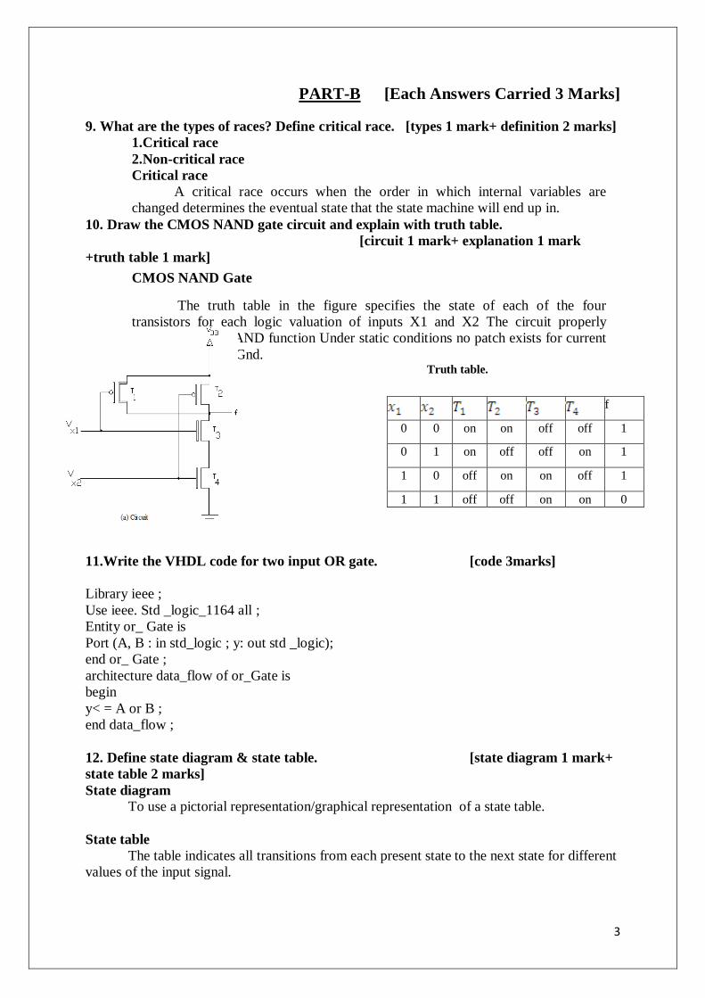
10. Draw the CMOS NAND gate circuit and explain with truth table.
[circuit 1 mark+ explanation 1 mark
+truth table 1 mark]
CMOS NAND Gate
The truth table in the figure specifies the state of each of the four
transistors for each logic valuation of inputs X1 and X2 The circuit properly
implements the NAND function Under static conditions no patch exists for current
flow from Vdd to Gnd. Truth table.
11.Write the VHDL code for two input OR gate. [code 3marks]
Library ieee ;
Use ieee. Std _logic_1164 all ;
Entity or_ Gate is
Port (A, B : in std_logic ; y: out std _logic);
end or_ Gate ;
architecture data_flow of or_Gate is
begin
y< = A or B ;
end data_flow ;
12. Define state diagram & state table. [state diagram 1 mark+
state table 2 marks]
State diagram
To use a pictorial representation/graphical representation of a state table.
State table
The table indicates all transitions from each present state to the next state for different
values of the input signal.
f
0 0 on on off off 1
0 1 on off off on 1
1 0 off on on off 1
1 1 off off on on 0

4
13. Write the VHDL code for D latch. [ code 3 marks]
library ieee;
use ieee.std_logic-1164.all;
entity latch is
port (d, clk :in std – logic;
q:out std – logic);
end latch;
architecture behavior of latch is
begin
process (d, clk)
begin
if clk=„1‟ then
q<=d;
end if
end process;
end behavior;
14. Define ASIC .What are the types of ASIC’s? [definition 2 marks +
types 1 mark]
ASIC
An ASIC is a Application Specific Integrated Circuit designed for a specific use for
general purpose use.
TYPES OF ASIC
1. Full custom ASICs
2. Semi custom ASICs
i. Standard cell based ASICs
ii Gate Array based ASICs
a. Channeled Gate array
b. Channel-less Gate Array
c. Embedded Gate array
15. Bring out a comparison between PROM, PLA & PAL . [any three
comparison 3 marks]
Comparison between PROM, PLA and PAL
SL. No PROM PLA PAL
1
AND array is fixed and OR
array is programmable
Both AND and OR
arrays are Programmable
OR array is fixed and AND
array is programmable
2 Cheaper and simple to use. Costliest and complex than
PAL and PROMs.
Cheaper and simpler
3
All minterms are decoded
AND array can be
programmed to get desired
minterms
AND array can be
programmed to get desired
minterms.
4
Only Boolean functions in
standard SOP form can be
implemented using PROM
Any Boolean functions in
SOP form can be
implemented using PLA
AnyBoolean functions in
SOP form can be
implemented using PAL.

5
16. Write a VHDL code for two input NANAD gate using process statement.
[code 3 marks]
VHDL code for two input NANAD gate using process statement
Library ieee ;
Use ieee. Std _logic_1164 all ;
Entity nand_ Gate is
Port (A, B : in std_logic ; y: out std _logic);
end nand_ Gate ;
architecture beh of nand_ Gate is
begin
process(a,b)
if(a =1 & b=1) then
y< = 0 ;
else
y<= 1;
end if;
end process;
end beh ;
PART-C [Each Answers Carried 10 Marks]
17 a) Draw the CMOS AND ,OR, NOR Gates and explain.
[diagram for each gates 6 marks+ explanation 4 marks]
CMOS AND GATE Circuit diagram Truth table
A CMOS AND gate is built by connecting a NAND gate to an inverter. This circuit has four MOS transistors. T1 and T2 are PMOS and T3 and T4 are NMOS. A
PMOS device will be turned ON when its gate input is low. An NMOS device will be turned
ON when its gate input is high. The circuit operation is explained below.
When both x1 and x2 are high:
When both x1 and x2 are highT1 and T2 are cut off and T3 and T4 are turned ON. Hence, the output is connected to the supply. ie. the output is high.
When x1 is high:
When x1 is high, T1 will turn off and T3 will conduct. Hence, the output is connected to ground ie. the output is low.
When x2 is high; Similarly, when x2 is high, T2 will turn off and T4 will conduct. Hence, the output is connected to ground ie. the output is low.
When both x1 and x2 are low
When both x1 and x2 are low T1 and T2 will conduct and T3 and T4 are turned OFF. Hence, the output is connected to the ground. i.e. the output is low.
f
0 0 on on off off 0
0 1 on off off on 0
1 0 off on on off 0
1 1 off off on on 1

6
CMOS OR GATE Circuit diagram Truth table
A CMOS OR gate is built by connecting a NOR gate to an inverter. This circuit has four MOS transistors. T1 and T2 are PMOS and T3 and T4 are NMOS. A
PMOS device will be turned ON when its gate input is low. An NMOS device will be turned
ON when its gate input is high. The circuit operation is explained below.
When both x1 and x2 are high:
When both x1 and x2 are highT1 and T2 are cut off and T3 and T4 are turned ON. Hence, the output is connected to the supply. ie. the output is high.
When x1 is low: When x1 is low, T1 will conduct and T3 will turn off. Hence, the output is connected to supply ie. the output is high.
When x2 is low:
Similarly, when x2 is low, T2 will conduct and T4 will turn off. Hence, the output is connected to supply ie. the output is high.
When both x1 and x2 are low When both x1 andx2 are low T1 and T2 will conduct and T3 and T4 are turned OFF. Hence, the output is connected to the ground. i.e. the output is low.
CMOS NOR GATE
Circuit diagram Truth table
This circuit has four MOS transistors. T1 and T2 are PMOS and T3 and T4 are NMOS. A
PMOS device will be turned ON when its gate input is low. An NMOS device will be turned
ON when its gate input is high. The circuit operation is explained below.
When both x1 and x2 are low: When both x1 and x2 are highT1 and T2 are turned ON and T3 and T4 are cut off. Hence, the output is connected to the supply. ie. the output is high.
When x1 is high:
When x1 is high, T1 will turn off and T3 will conduct. Hence, the output is connected to ground ie. the output is low.
f
0 0 on on off off 0
0 1 on off off on 1
1 0 off on on off 1
1 1 off off on on 1
f
0 0 on on off off 1
0 1 on off off on 0
1 0 off on on off 0
1 1 off off on on 0
7
When x2 is high; Similarly, when x2 is high, T2 will turn off and T4 will conduct. Hence, the output is
connected to ground ie. the output is low.
When both x1 and x2 are high: When both x1 and x2 are highT1 and T2 are turned ON and T3 and T4 are cut off. Hence, the output is connected to the supply. ie. the output is high.
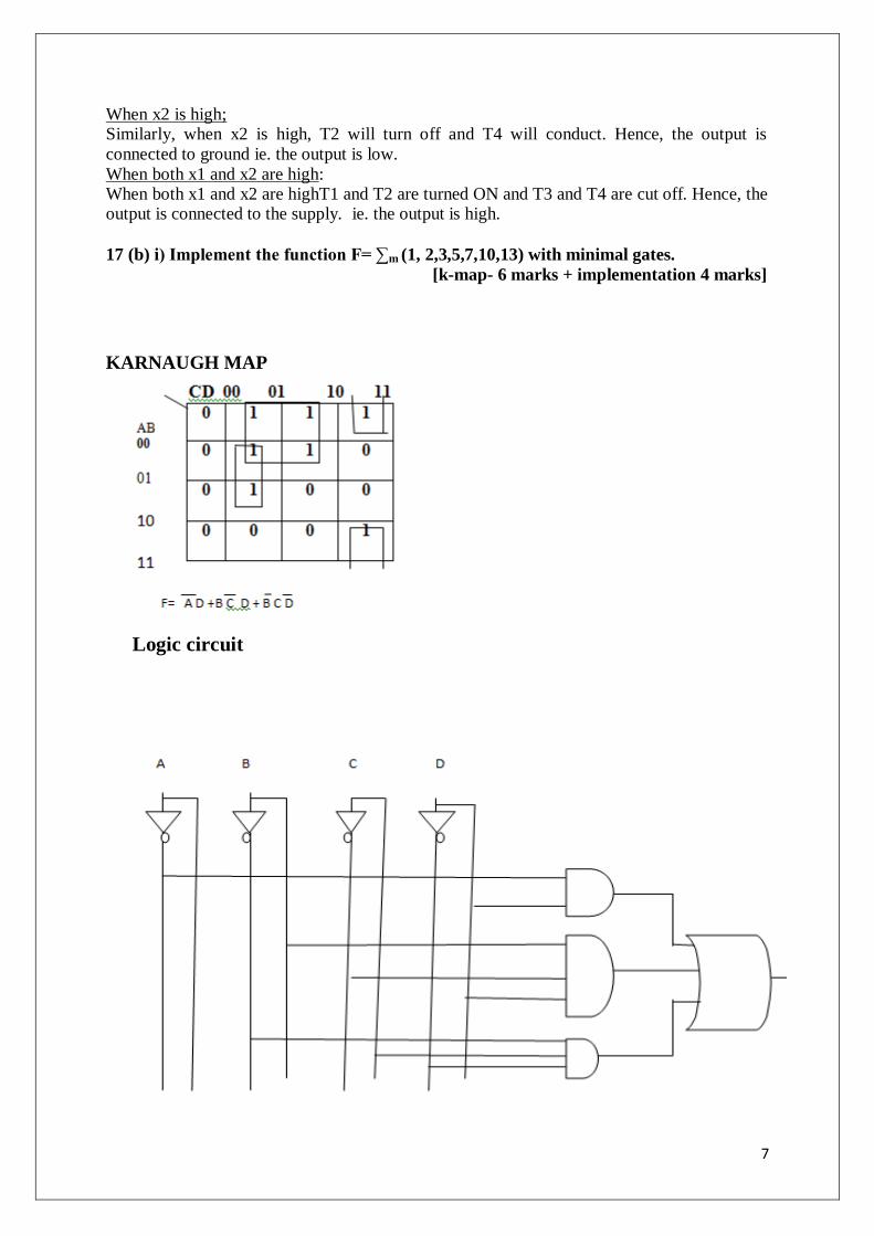
17 (b) i) Implement the function F= ∑m (1, 2,3,5,7,10,13) with minimal gates.
[k-map- 6 marks + implementation 4 marks]
KARNAUGH MAP
Logic circuit
8
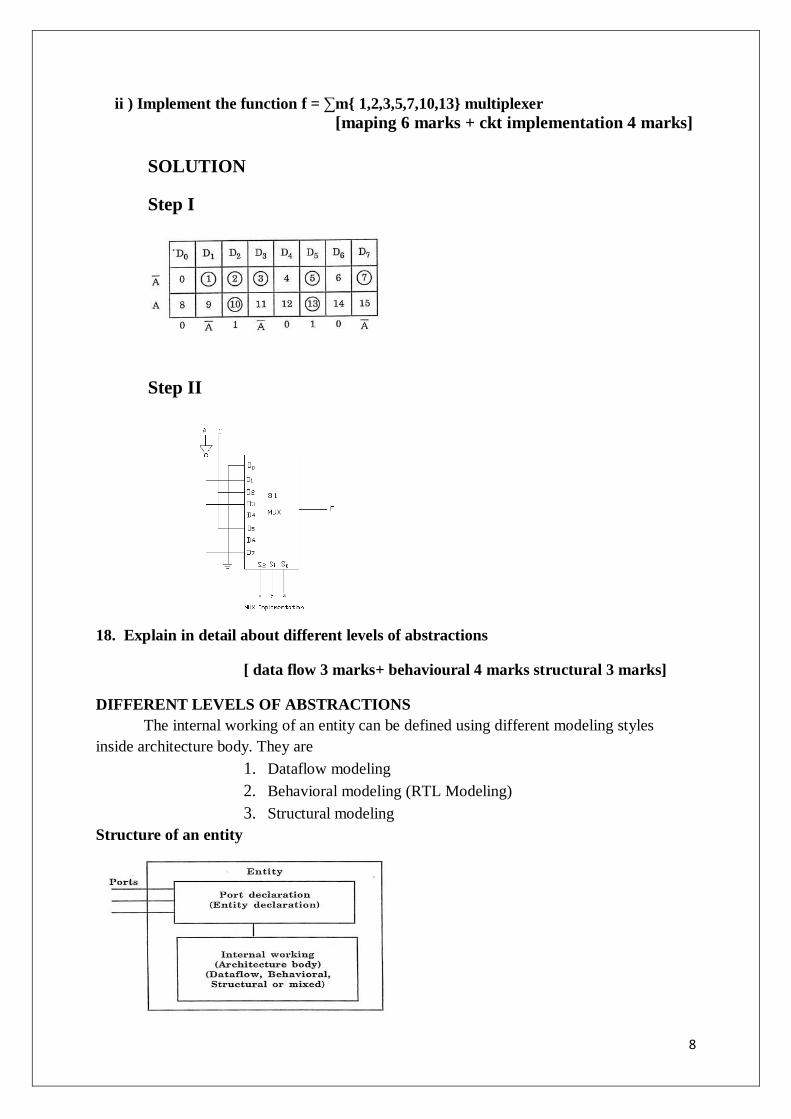
ii ) Implement the function f = ∑m{ 1,2,3,5,7,10,13} multiplexer
[maping 6 marks + ckt implementation 4 marks]
SOLUTION
Step I
Step II
18. Explain in detail about different levels of abstractions
[ data flow 3 marks+ behavioural 4 marks structural 3 marks]
DIFFERENT LEVELS OF ABSTRACTIONS
The internal working of an entity can be defined using different modeling styles
inside architecture body. They are
1. Dataflow modeling
2. Behavioral modeling (RTL Modeling)
3. Structural modeling
Structure of an entity
9
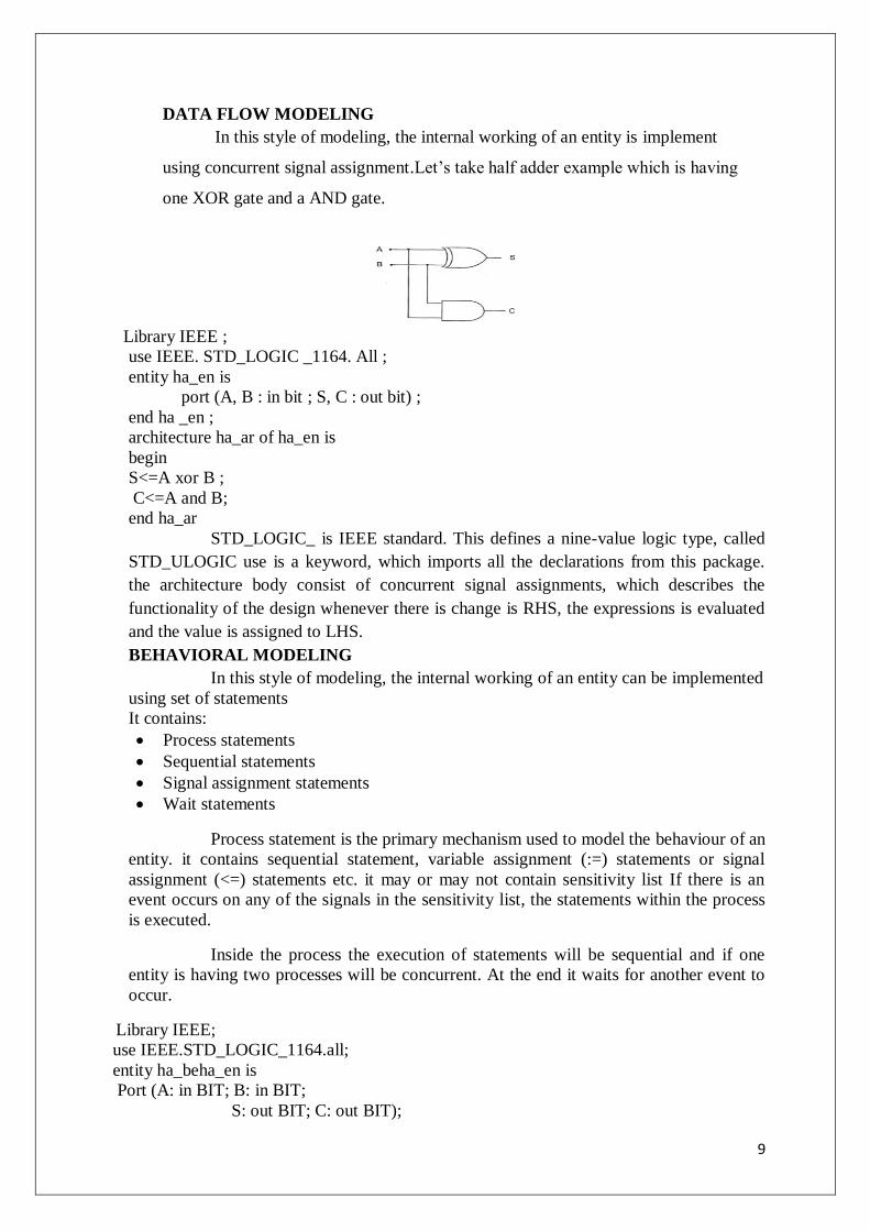
DATA FLOW MODELING
In this style of modeling, the internal working of an entity is implement
using concurrent signal assignment.Let‟s take half adder example which is having
one XOR gate and a AND gate.
Library IEEE ;
use IEEE. STD_LOGIC _1164. All ;
entity ha_en is
port (A, B : in bit ; S, C : out bit) ;
end ha _en ;
architecture ha_ar of ha_en is
begin
S<=A xor B ;
C<=A and B;
end ha_ar
STD_LOGIC_ is IEEE standard. This defines a nine-value logic type, called
STD_ULOGIC use is a keyword, which imports all the declarations from this package.
the architecture body consist of concurrent signal assignments, which describes the
functionality of the design whenever there is change is RHS, the expressions is evaluated
and the value is assigned to LHS.
BEHAVIORAL MODELING
In this style of modeling, the internal working of an entity can be implemented
using set of statements
It contains:
Process statements
Sequential statements
Signal assignment statements
Wait statements
Process statement is the primary mechanism used to model the behaviour of an
entity. it contains sequential statement, variable assignment (:=) statements or signal
assignment (<=) statements etc. it may or may not contain sensitivity list If there is an
event occurs on any of the signals in the sensitivity list, the statements within the process
is executed.
Inside the process the execution of statements will be sequential and if one
entity is having two processes will be concurrent. At the end it waits for another event to
occur.
Library IEEE;
use IEEE.STD_LOGIC_1164.all;
entity ha_beha_en is
Port (A: in BIT; B: in BIT;
S: out BIT; C: out BIT);
10
end ha_beha en;
architecture ha_beha_ar of ha_beha_en is
begin
process_beh:
process(A,B)
begin
S<=A xor B;
C<=A and B:
end process process_beh:
end ha_beha_ar;
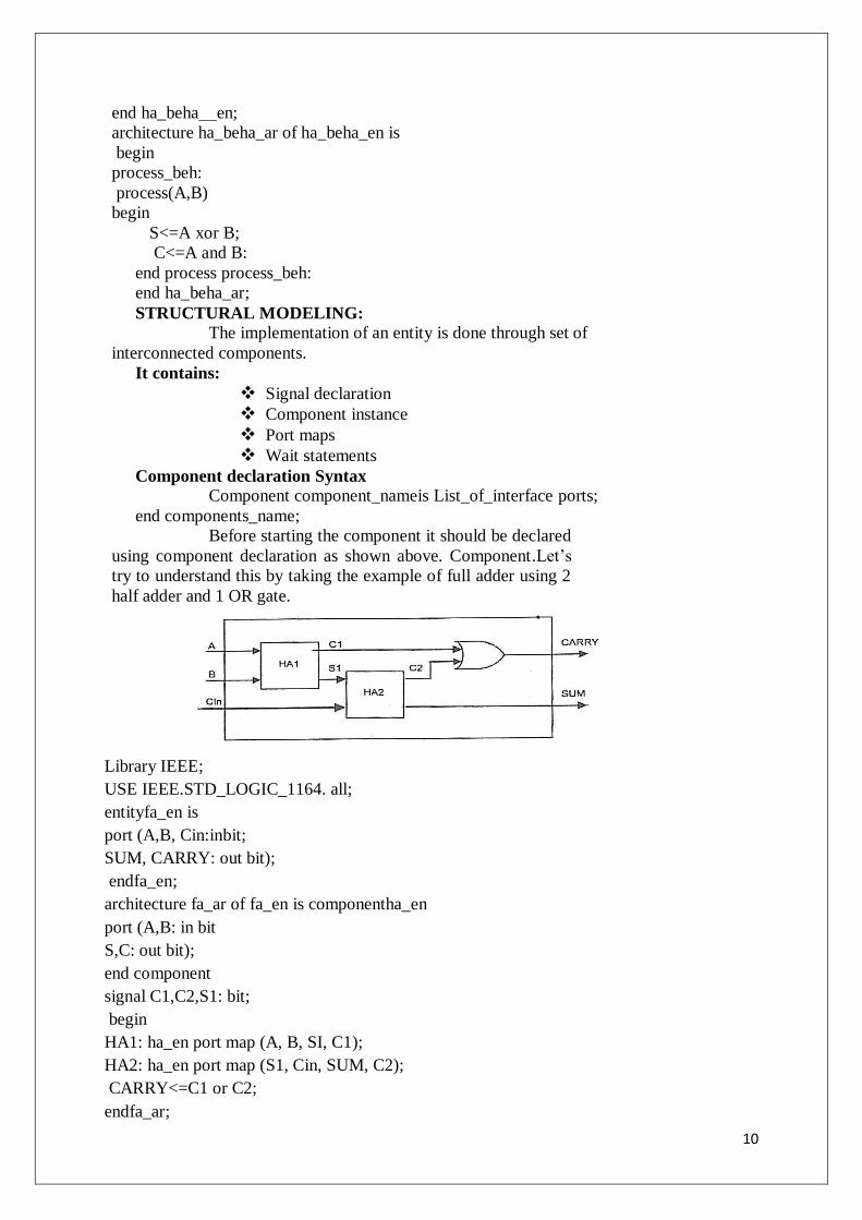
STRUCTURAL MODELING:
The implementation of an entity is done through set of
interconnected components.
It contains:
Signal declaration
Component instance
Port maps
Wait statements
Component declaration Syntax
Component component_nameis List_of_interface ports;
end components_name;
Before starting the component it should be declared
using component declaration as shown above. Component.Let‟s
try to understand this by taking the example of full adder using 2
half adder and 1 OR gate.
Library IEEE;
USE IEEE.STD_LOGIC_1164. all;
entityfa_en is
port (A,B, Cin:inbit;
SUM, CARRY: out bit);
endfa_en;
architecture fa_ar of fa_en is componentha_en
port (A,B: in bit
S,C: out bit);
end component
signal C1,C2,S1: bit;
begin
HA1: ha_en port map (A, B, SI, C1);
HA2: ha_en port map (S1, Cin, SUM, C2);
CARRY<=C1 or C2;
endfa_ar;
11
(b) ( i) Write the VHDL code for 4:2 Encoder. [any one modelling
method -code 5 marks]
VHDL code for 4:2 Encoder
library IEEE ;
use IEEE. STD_LOGIC _1164. ALL ; use IEEE. STD_ LOGIC _ARITH. ALL ;
use IEEE. STD_LOGIC _UNSIGNED. ALL ;
entity encod is
Port (a : in STD_LOGIC _VECTOR (3 downto 0) ;
B : out STD_LOGIC_VECTOR (1 down to 0)) ;
end encod ;
architecture Behavioral of encod is begin
process(a)
begin
if (a(0) = „1‟) then
b<= “00”;
elsif (a(1) = „1‟) then
b<=”01”;
elsif (a(2) = „1‟) then
b<=”10” ;
elsif (a(3) = „1‟) then
b<=”11” ;
end if ;
end process ;
end Behavioral ;
(ii) Write a VHDL code for 1:4 demux.
[any one modelling method -code 5 marks]
library IEEE ;
use IEEE. STD_LOGIC _1164. ALL ;
use IEEE. STD_ LOGIC _ARITH. ALL ;
use IEEE. STD_LOGIC _UNSIGNED. ALL ;
entity DeMUX is
port( X: in std_logic;
sel:in std_logic_vector (1 downto 0);
A,B,C,D: out std_logic);
end DeMUX;
architecture behavior of DeMUX is
begin
process(sel, X)
begin
case sel is
When “00”=> A <=X;B <=‟0‟;C <=‟0‟;D <=‟0‟;
When “01” => B <=X;A <=0;C <=‟0‟;D <=‟0‟;
When “10”=> C <=X;A <=‟0‟;B <=‟0‟;D <=‟0‟;
When others=> D <=X;A <=‟0‟;B <=‟0‟;C <=‟0‟;end case;
end process; end behavior;
12
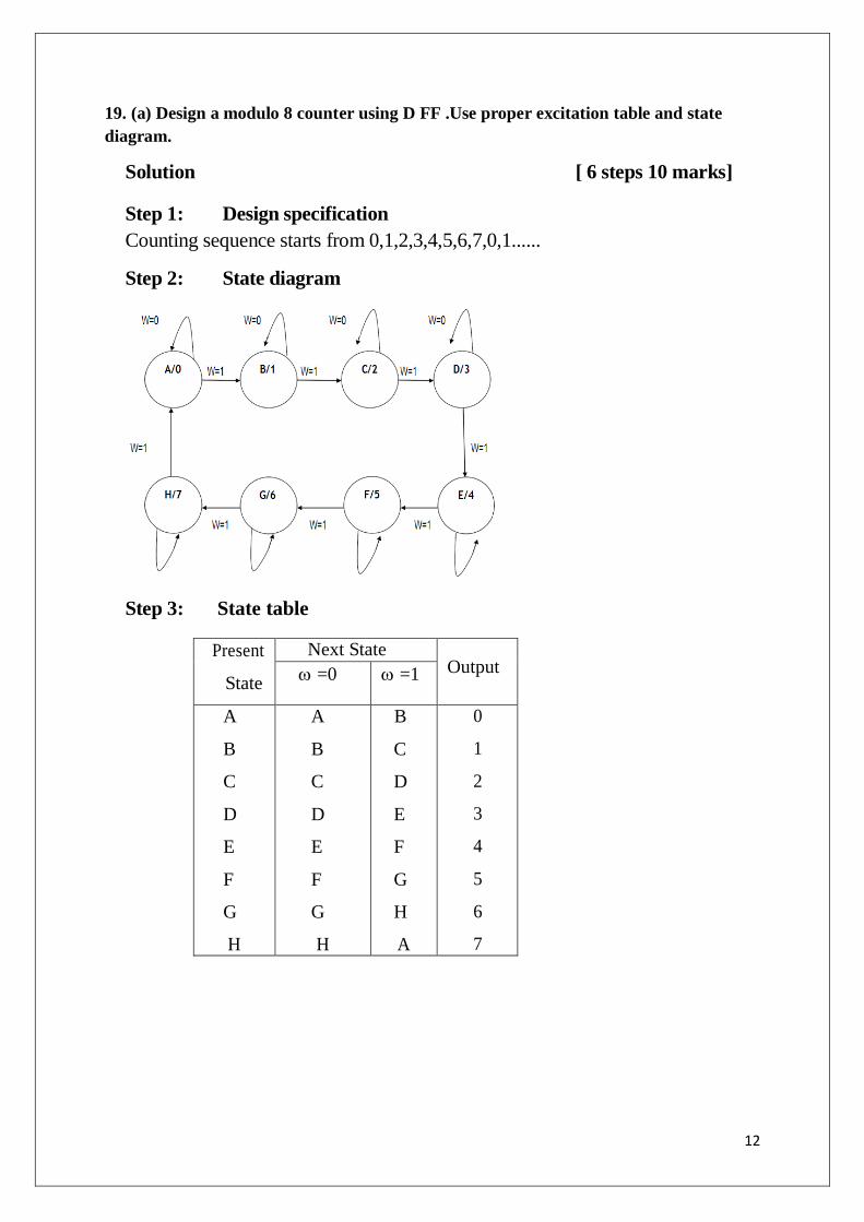
19. (a) Design a modulo 8 counter using D FF .Use proper excitation table and state
diagram.
Solution [ 6 steps 10 marks]
Step 1: Design specification
Counting sequence starts from 0,1,2,3,4,5,6,7,0,1......
Step 2: State diagram
Step 3: State table
Present
State
Next State Output =0 =1
A
B
C
D
E
F
G
H
A
B
C
D
E
F
G
H
B
C
D
E
F
G
H
A
0
1
2
3
4
5
6
7
13
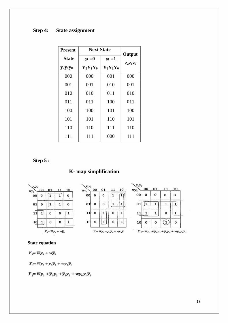
Step 4: State assignment
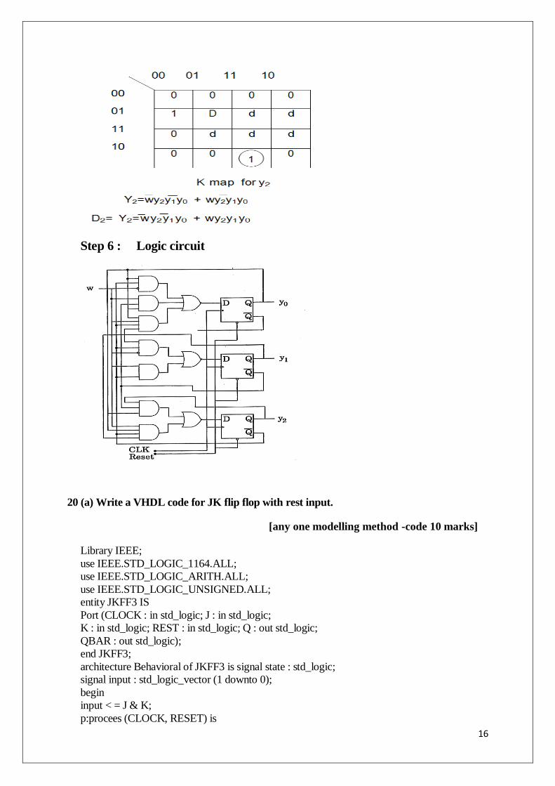
Step 5 :
K- map simplification
State equation
Present
State
y2y1y0
Next State Output
z2z1z0
=0
Y2Y1Y0
=1
Y2Y1Y0
000 000 001 000
001 001 010 001
010 010 011 010
011 011 100 011
100 100 101 100
101 101 110 101
110 110 111 110
111 111 000 111
14
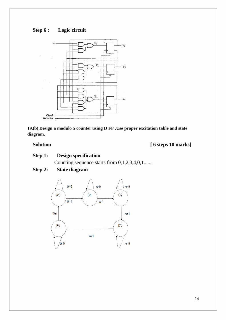
Step 6 : Logic circuit
19.(b) Design a modulo 5 counter using D FF .Use proper excitation table and state
diagram.
Solution [ 6 steps 10 marks]
Step 1: Design specification
Counting sequence starts from 0,1,2,3,4,0,1......
Step 2: State diagram
15
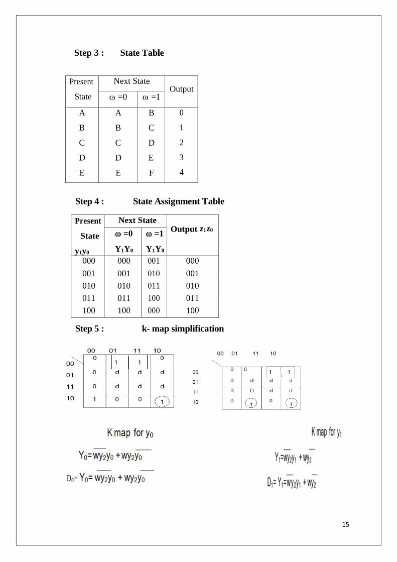
Step 3 : State Table
Step 4 : State Assignment Table
Present
State
y1y0
Next State Output z1z0
=0
Y1Y0
=1
Y1Y0
000 000 001 000
001 001 010 001
010 010 011 010
011 011 100 011
100 100 000 100
Step 5 : k- map simplification
Present
State
Next State Output
=0 =1
A
B
C
D
E
A
B
C
D
E
B
C
D
E
F
0
1
2
3
4
16
Step 6 : Logic circuit
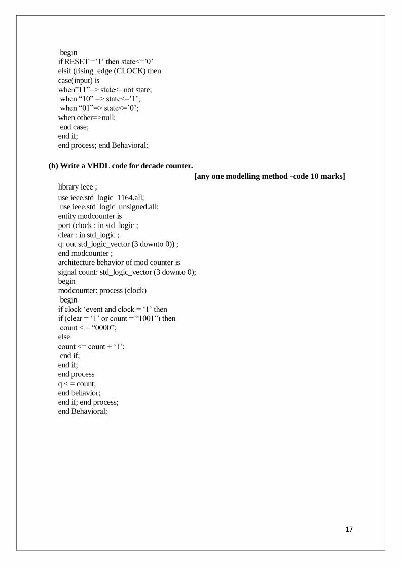
20 (a) Write a VHDL code for JK flip flop with rest input.
[any one modelling method -code 10 marks]
Library IEEE;
use IEEE.STD_LOGIC_1164.ALL;
use IEEE.STD_LOGIC_ARITH.ALL;
use IEEE.STD_LOGIC_UNSIGNED.ALL;
entity JKFF3 IS
Port (CLOCK : in std_logic; J : in std_logic;
K : in std_logic; REST : in std_logic; Q : out std_logic;
QBAR : out std_logic);
end JKFF3;
architecture Behavioral of JKFF3 is signal state : std_logic;
signal input : std_logic_vector (1 downto 0);
begin
input < = J & K;
p:procees (CLOCK, RESET) is
17
begin
if RESET =‟1‟ then state<=‟0‟
elsif (rising_edge (CLOCK) then
case(input) is
when”11”=> state<=not state;
when “10” => state<=‟1‟;
when “01”=> state<=‟0‟;
when other=>null;
end case;
end if;
end process; end Behavioral;
(b) Write a VHDL code for decade counter.
[any one modelling method -code 10 marks]
library ieee ;
use ieee.std_logic_1164.all;
use ieee.std_logic_unsigned.all;
entity modcounter is
port (clock : in std_logic ;
clear : in std_logic ;
q: out std_logic_vector (3 downto 0)) ;
end modcounter ;
architecture behavior of mod counter is
signal count: std_logic_vector (3 downto 0);
begin
modcounter: process (clock)
begin
if clock „event and clock = „1‟ then
if (clear = „1‟ or count = “1001”) then
count < = “0000”;
else
count <= count + „1‟;
end if;
end if;
end process
q < = count;
end behavior;
end if; end process;
end Behavioral;
18
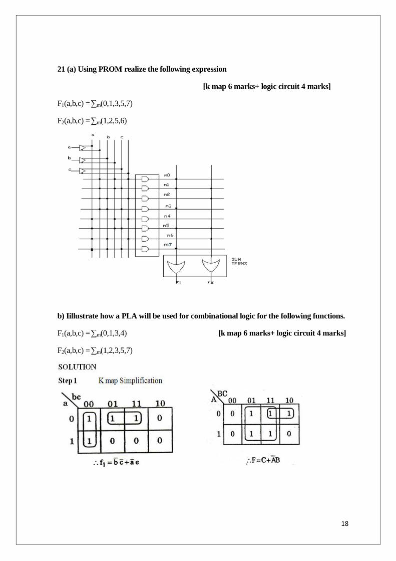
21 (a) Using PROM realize the following expression
[k map 6 marks+ logic circuit 4 marks]
F1(a,b,c) = ∑m(0,1,3,5,7)
F2(a,b,c) = ∑m(1,2,5,6)
b) Iillustrate how a PLA will be used for combinational logic for the following functions.
F1(a,b,c) = ∑m(0,1,3,4) [k map 6 marks+ logic circuit 4 marks]
F2(a,b,c) = ∑m(1,2,3,5,7)
19
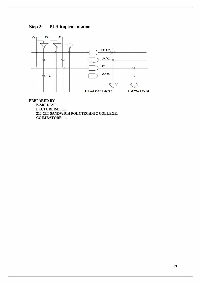
Step 2: PLA implementation
PREPARED BY
K.SRI DEVI,
LECTURER/ECE,
210-CIT SANDWICH POLYTECHNIC COLLEGE,
COIMBATORE-14.