asic design (7v81)zhoud/lecture1.pdfgate-array–based asics a gate array, masked gate array, mga,...
TRANSCRIPT

ASIC Design (7v81)
Spring 2000Spring 2000

Lecture 1 (1/21/2000)
nn General informationGeneral information
General description
nn We study the hardware structure, synthesis method, design We study the hardware structure, synthesis method, design methodology, and design flow from the application to an methodology, and design flow from the application to an ASIC chip.ASIC chip.
nn A project is developed to design an FIR digital filter. The A project is developed to design an FIR digital filter. The students are required to start from a filter algorithm and the students are required to start from a filter algorithm and the system specifications to complete an ASIC design.system specifications to complete an ASIC design.

Instructor information
uu Instructor D. Zhou Instructor D. Zhou uu Email: [email protected]: [email protected] Phone: 972 883 4392Phone: 972 883 4392uu Office: EC2.510Office: EC2.510uu Class room: EC 2.120Class room: EC 2.120

TA and office hours
nn TA: Naveen MysoreTA: Naveen Mysoreuu Phone : (214) 575Phone : (214) 575--32463246uu Email : [email protected] : [email protected] Office : EC: 2.322Office : EC: 2.322
nn Office hour (TA) : Thursday 7pm Office hour (TA) : Thursday 7pm -- 8pm 8pm nn Office hour (instructor): after class meetingOffice hour (instructor): after class meeting

Text book
nn ApplicationApplication--Specific Integrated Circuits, Michael John Specific Integrated Circuits, Michael John Sebastian Smith, Addison Wesley, ISBN: 0Sebastian Smith, Addison Wesley, ISBN: 0--201201--5002250022

Prerequisite
nn VLSI design knowledgeVLSI design knowledgenn VHDL or similar hardware design languageVHDL or similar hardware design languagenn C language C language nn Physical layout, circuit simulation and logic verificationPhysical layout, circuit simulation and logic verification

Project requirement
nn Specification of the projectSpecification of the projectnn Clear presentation Clear presentation nn Technique details of the designed systemTechnique details of the designed systemnn Well written reportWell written reportnn Maximum team size: 2Maximum team size: 2
Grading
nn homework 20%homework 20%nn reading report 10%reading report 10%nn attendance and quiz 10%attendance and quiz 10%nn middle term project 20%middle term project 20%nn final project 40%final project 40%nn 8585--100 100 -->A, 70>A, 70--84 84 -->B, 60>B, 60--69 69 -->C, and below 60 >C, and below 60 --> fail> fail

Lecture 2
nn Introduction to ASIC designIntroduction to ASIC design

INTRODUCTION TO ASICs
Key concepts: The difference between full-custom and semicustom ASICs • The difference between standard-cell, gate-array, and programmable ASICs •ASIC design flow •ASIC cell library
ASIC (“a-sick”) is an Application-Specific Integrated CircuitOrigin of ASICs: the standard parts , initially used to design microelectronic systems , were gradually replaced with a combination of glue logic , custom ICs , dynamic random-access memory ( DRAMand static RAM ( SRAM )Application-specific standard products ( ASSPs ) are a cross between standard parts and ASICs

Types of ASICsFull-Custom ASICs
Full-custom offers the highest performance and lowest part cost (smallest die size) with the
disadvantages of increased design time, complexity, design expense, and highest risk.
Examples of full-custom ICs or ASICs are requirements for high-voltage (automobile),
analog/digital (communications), or sensors and actuators
Standard-Cell–Based ASICs
A cell based ASIC die with a single cell area together with four fixed blocks

Design flowDesign flow
ASIC design flow. Steps 1–4 are logical design , and steps 5–9 are physical design

Full custom design and ASICs
nn Full custom designFull custom designuu high performance and high design costhigh performance and high design costuu examples: PC and workstation CPUexamples: PC and workstation CPU
nn ASICsASICsuu low design cost and compromised performancelow design cost and compromised performanceuu examples: an I/O circuit or a special DSP chipexamples: an I/O circuit or a special DSP chip

ASIC hardware architectures
nn prepre--design cells and functional blocksdesign cells and functional blocksnn uniformed circuits and devicesuniformed circuits and devicesnn uniformed interconnect structuresuniformed interconnect structuresnn programmable interconnectsprogrammable interconnects
CellCell--based ASICbased ASIC (( CBICCBIC —— ““seasea--bickbick””))
Standard cellsStandard cellsPossibly megacells , megafunctions , fullPossibly megacells , megafunctions , full--custom blocks , systemcustom blocks , systemlevel macros level macros
( Slms ), fixed blocks , cores , or functional standard block( Slms ), fixed blocks , cores , or functional standard blocks ( fsbs s ( fsbs ))
All mask layers are customizedAll mask layers are customized—— transistors and interconnecttransistors and interconnectCustom blocks can be embeddedCustom blocks can be embeddedManufacturing lead time is about eight weeksManufacturing lead time is about eight weeks

GateGate--arrayarray––based ASICsbased ASICs
A A gate arraygate array, , masked gate arraymasked gate array, , MGAMGA, or , or prepre--diffused arraydiffused array uses uses macrosmacros (( booksbooks ) to ) to
reduce reduce turnaround timeturnaround time and comprises a and comprises a base arraybase array made from a made from a base base cellcell or or primitive primitive
cellcellTypes of gate array Types of gate array –– based ASIC:based ASIC:
Channeled gate arrays Channeled gate arrays Channel less gate arrays Channel less gate arrays Structured gate arrays Structured gate arrays
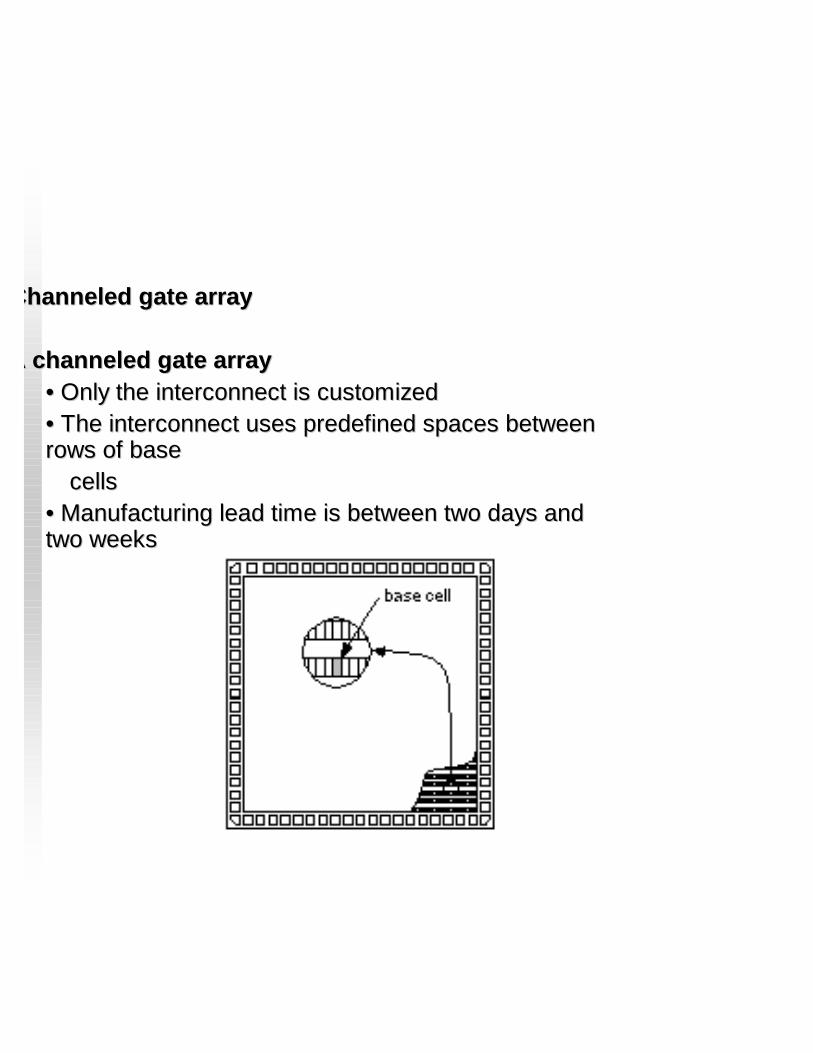
Channeled gate arrayChanneled gate array
A A channeled gate array channeled gate array ••Only the interconnect is customized Only the interconnect is customized ••The interconnect uses predefined spaces between The interconnect uses predefined spaces between rows of base rows of base
cells cells ••Manufacturing lead time is between two days and Manufacturing lead time is between two days and two weekstwo weeks

Channelless gate array Channelless gate array
channelless gate arraychannelless gate array (( channelchannel--free gate arrayfree gate array , , seasea--ofof--gates arraygates array , or , or SOGSOGarray) array) •• Only some (the top few) mask layers are customizedOnly some (the top few) mask layers are customized—— the interconnectthe interconnect•• Manufacturing lead time is between two days and two weeksManufacturing lead time is between two days and two weeks

Structured gate array Structured gate array
An embedded An embedded gate arraygate array or or structured gate arraystructured gate array ( masterslice or masterimage )( masterslice or masterimage )•• Only the interconnect is customized Only the interconnect is customized •• Custom blocks (the same for each design) can be embedded Custom blocks (the same for each design) can be embedded •• Manufacturing lead time is between two days and two weeksManufacturing lead time is between two days and two weeks

Programmable logic devicesProgrammable logic devices
Programmable logic deviceProgrammable logic device (( PLDPLD ))No customized mask layers or logic cellsNo customized mask layers or logic cellsFast design turnaround Fast design turnaround A single large block of programmable interconnect A single large block of programmable interconnect A matrix of logic macro cells that usually consist of programmA matrix of logic macro cells that usually consist of programmable array logic able array logic
followedfollowedby a flipby a flip--flop or latchflop or latch

FieldField--programmable gate arraysprogrammable gate arrays
FieldField--programmable gate arrayprogrammable gate array (( FPGAFPGA ) or ) or complex PLDcomplex PLDNone of the mask layers are customizedNone of the mask layers are customizedA method for programming the basic logic cells and the intercoA method for programming the basic logic cells and the interconnectnnectThe core is a regular array of programmable basic logic cells The core is a regular array of programmable basic logic cells that can implement that can implement combinational as well as sequential logic (flipcombinational as well as sequential logic (flip--flops)flops)A matrix of programmable interconnect surrounds the basic logiA matrix of programmable interconnect surrounds the basic logic cellsc cellsProgrammable I/O cells surround the coreProgrammable I/O cells surround the coreDesign turnaround is a few hoursDesign turnaround is a few hours

Design entryDesign entry . using a . using a hardware description languagehardware description language (( VHDLVHDL ) or ) or Schematic entry Schematic entry Logic synthesisLogic synthesis . produces a . produces a netlistnetlist —— logic cells and their connections logic cells and their connections System partitioningSystem partitioning . divide a large system into functional blocks. divide a large system into functional blocksPrelayout simulationPrelayout simulation . check to see if the design functions correctly . check to see if the design functions correctly FloorplanningFloorplanning . arrange the blocks of the netlist on the chip . arrange the blocks of the netlist on the chip PlacementPlacement . decide the locations of cells in a block . decide the locations of cells in a block RoutingRouting . make the connections between cells and blocks . make the connections between cells and blocks ExtractionExtraction . determine the resistance and capacitance of the interconnect . determine the resistance and capacitance of the interconnect Postlayout simulationPostlayout simulation . check to see the design still works with the added . check to see the design still works with the added Loads of the interconnect Loads of the interconnect

ASIC cell librariesASIC cell libraries
DDesign kitesign kit from thefrom the ASIC vendorASIC vendor
Usually aUsually a phantom libraryphantom library —— the cells are empty boxes, orthe cells are empty boxes, or phantomsphantoms , , youyou hand hand offoff your design to the ASIC vendor and they performyour design to the ASIC vendor and they perform phantom instantiationphantom instantiation
((Synopsys CBA)Synopsys CBA)
AsicAsic--vendor libraryvendor library from afrom a library vendorlibrary vendor
Involves aInvolves a buybuy--oror--build decisionbuild decisionYou need aYou need a qualified cell libraryqualified cell library (qualified by the(qualified by the ASIC foundryASIC foundryIf you own the masks (theIf you own the masks (the toolingtooling ) you have a) you have a customercustomer--owned toolingowned tooling ( COT( COT , ,
pronounced pronounced ““seesee--ohoh--teetee””) solution (which is becoming very popular)) solution (which is becoming very popular)

Building own cell libraryBuilding own cell libraryInvolves a complexInvolves a complex library developmentlibrary development process:process:
Cell layoutCell layoutBehavioral modelBehavioral modelVerilog/VHDL modelVerilog/VHDL modelTiming model Timing model Test strategy Test strategy Characterization Characterization Circuit extraction Circuit extraction Process control monitorsProcess control monitors (( pcmspcms ) or) or dropdrop--insinsCell schematicCell schematicCell icon Cell icon Layout versus schematicLayout versus schematic ( LVS( LVS ) check ) check Logic synthesis Logic synthesis RetargetingRetargetingWireWire--load modelload modelRouting modelRouting modelPhantomPhantom

Reading assignment
nn Chapter oneChapter onenn Write a one page reading summaryWrite a one page reading summarynn Due: in a weekDue: in a week