analog applications journal q2 2011 - slyt409
TRANSCRIPT

Texas Instruments Incorporated
High-Performance Analog Products
Analog ApplicationsJournal
Second Quarter, 2011
© Copyright 2011 Texas Instruments

Texas Instruments Incorporated
2
Analog Applications JournalHigh-Performance Analog Products www.ti.com/aaj 2Q 2011
IMPORTANT NOTICE
Texas Instruments Incorporated and its subsidiaries (TI) reserve the right to make corrections, modifications, enhancements, improvements, and other changes to its products and services at any time and to discontinue any product or service without notice. Customers should obtain the latest relevant information before placing orders and should verify that such information is current and complete. All products are sold subject to TI’s terms and conditions of sale supplied at the time of order acknowledgment.
TI warrants performance of its hardware products to the specifications applicable at the time of sale in accordance with TI’s standard warranty. Testing and other quality control techniques are used to the extent TI deems necessary to support this warranty. Except where mandated by government requirements, testing of all parameters of each product is not necessarily performed.
TI assumes no liability for applications assistance or customer product design. Customers are responsible for their products and applications using TI components. To minimize the risks associated with customer products and applications, customers should provide adequate design and operating safeguards.
TI does not warrant or represent that any license, either express or implied, is granted under any TI patent right, copyright, mask work right, or other TI intellectual property right relating to any combination, machine, or process in which TI products or services are used. Information published by TI regarding third-party products or services does not constitute a license from TI to use such products or services or a warranty or endorsement thereof. Use of such information may require a license from a third party under the patents or other intellectual property of the third party, or a license from TI under the patents or other intellectual property of TI.
Reproduction of TI information in TI data books or data sheets is permissible only if reproduction is without alteration and is accompanied by all associated warranties, conditions, limitations, and notices. Reproduction of this information with alteration is an unfair and deceptive business practice. TI is not responsible or liable for such altered documentation. Information of third parties may be subject to additional restrictions.
Resale of TI products or services with statements different from or beyond the parameters stated by TI for that product or service voids all express and any implied warranties for the associated TI product or service and is an unfair and deceptive business practice. TI is not responsible or liable for any such statements.
TI products are not authorized for use in safety-critical applications (such as life support) where a failure of the TI product would reasonably be expected to cause severe personal injury or death, unless officers of the parties have executed an agreement specifically governing such use. Buyers represent that they have all necessary expertise in the safety and regulatory ramifications of their applications, and acknowledge and agree that they are solely responsible for all legal, regulatory and safety-related requirements concerning their products and any use of TI products in such safety-critical applications, notwithstanding any applications-related information or support that may be provided by TI. Further, Buyers must fully indemnify TI and its representatives against any damages arising out of the use of TI products in such safety-critical applications.
TI products are neither designed nor intended for use in military/aerospace applications or environments unless the TI products are specifically designated by TI as military-grade or "enhanced plastic." Only products designated by TI as military-grade meet military specifications. Buyers acknowledge and agree that any such use of TI products which TI has not designated as military-grade is solely at the Buyer's risk, and that they are solely responsible for compliance with all legal and regulatory requirements in connection with such use.
TI products are neither designed nor intended for use in automotive applications or environments unless the specific TI products are designated by TI as compliant with ISO/TS 16949 requirements. Buyers acknowledge and agree that, if they use any non-designated products in automotive applications, TI will not be responsible for any failure to meet such requirements.
Following are URLs where you can obtain information on other Texas Instruments products and application solutions:
Products Audio www.ti.com/audio Amplifiers amplifier.ti.com Data Converters dataconverter.ti.com DLP® Products www.dlp.comDSP dsp.ti.com Clocks and Timers www.ti.com/clocksInterface interface.ti.com Logic logic.ti.com Power Managementt power.ti.com Microcontrollers microcontroller.ti.com RFID www.ti-rfid.comRF/IF and ZigBee® Solutions www.ti.com/lprf
Applications Communications and Telecom www.ti.com/communicationsComputers and Peripherals www.ti.com/computers Consumer Electronics www.ti.com/consumer-appsEnergy and Lighting www.ti.com/energyIndustrial www.ti.com/industrialMedical www.ti.com/medicalSecurity www.ti.com/security Space, Avionics and Defense www.ti.com/space-avionics-defense Transportation and Automotive www.ti.com/automotive Video and Imaging www.ti.com/video Wireless www.ti.com/wireless-apps
TI E2E™ Community Home Page e2e.ti.comMailing Address: Texas Instruments, Post Office Box 655303, Dallas, Texas 75265
Copyright © 2011, Texas Instruments Incorporated

Texas Instruments Incorporated
3
Analog Applications Journal 2Q 2011 www.ti.com/aaj High-Performance Analog Products
Introduction . . . . . . . . . . . . . . . . . . . . . . . . . . . . . . . . . . . . . . . . . . . . . . . . . . . . . . . . . . . . . . .4
Data AcquisitionThe IBIS model, Part 3: Using IBIS models to investigate signal-integrity issues . . . . .5
TI is developing a new arsenal of digital input/output buffer information specification (IBIS) simulation models to meet a variety of customer needs. This article, the third of a three-part series, shows how to use an IBIS model to extract important variables for signal-integrity calculations and PCB design solutions.
Power ManagementImplementation of microprocessor-controlled, wide-input-voltage, SMBus smart battery charger . . . . . . . . . . . . . . . . . . . . . . . . . . . . . . . . . . . . . . . . . . . . . . . . . . . . . . .11
For the utmost in system flexibility, using microprocessors to control Li-ion battery chargers is becoming very popular. This article describes the design of a microprocessor-based charger that can handle an input of up to 55 V and can supply an output charging voltage of 5 to 51 V at up to 10 A. Both the hardware and software have been tested to aid designers in quickly prototyping their own solutions.
Benefits of a coupled-inductor SEPIC converter . . . . . . . . . . . . . . . . . . . . . . . . . . . . . . . .14The SEPIC topology provides a convenient solution when a converter must operate in both buck and boost modes. While the SEPIC has few active components and a simple controller and produces relatively low noise, choosing the inductor configuration can sometimes be a challenge. This article discusses the impact of using coupled and uncoupled inductor windings in a SEPIC design.
IQ: What it is, what it isn’t, and how to use it . . . . . . . . . . . . . . . . . . . . . . . . . . . . . . . . . . .18A device’s quiescent current (IQ) is an important parameter for energy-efficient designs using low-power DC/DC converters. This article explains how IQ can be only a portion of the system’s standby power drain and the importance of looking for all possible input-current paths. Measurement techniques are also covered to help designers avoid common measurement errors.
Backlighting the tablet PC . . . . . . . . . . . . . . . . . . . . . . . . . . . . . . . . . . . . . . . . . . . . . . . . . . .23Backlighting is one of the most power-hungry components of a tablet PC. This article gives guidance on how to select the optimal WLED driver and LED-string configuration to meet system requirements without sacrificing efficiency and therefore battery life. Included are efficiency comparisons for several LED configurations.
Challenges of designing high-frequency, high-input-voltage DC/DC converters . . . .28A DC/DC converter designed to operate at 1 or 2 MHz can reduce board space, but the higher frequency impacts the power-supply system in more ways than just its size and efficiency. This article presents several design examples that demonstrate the benefits and challenges of switching at higher frequencies.
Index of Articles . . . . . . . . . . . . . . . . . . . . . . . . . . . . . . . . . . . . . . . . . . . . . . . . . . . . . . . . . .32
TI Worldwide Technical Support . . . . . . . . . . . . . . . . . . . . . . . . . . . . . . . . . . . . . . . . . .38
Contents
To view past issues of the Analog Applications Journal, visit the Web site
www.ti.com/aaj

Texas Instruments Incorporated
4
Analog Applications JournalHigh-Performance Analog Products www.ti.com/aaj 2Q 2011
Analog Applications Journal is a collection of analog application articles designed to give readers a basic understanding of TI products and to provide simple but practical examples for typical applications. Written not only for design engineers but also for engineering managers, technicians, system designers and marketing and sales personnel, the book emphasizes general application concepts over lengthy mathematical analyses.
These applications are not intended as “how-to” instructions for specific circuits but as examples of how devices could be used to solve specific design requirements. Readers will find tutorial information as well as practical engineering solutions on components from the following categories:
• Data Acquisition
• Power Management
• Interface (Data Transmission)
• Amplifiers: Audio
• Amplifiers: Op Amps
• Low-Power RF
• General Interest
Where applicable, readers will also find software routines and program structures. Finally, Analog Applications Journal includes helpful hints and rules of thumb to guide readers in preparing for their design.
Introduction

5
Analog Applications Journal
Texas Instruments Incorporated
2Q 2011 www.ti.com/aaj High-Performance Analog Products
The IBIS model, Part 3: Using IBIS models to investigate signal-integrity issues
This article is the third of a three-part series on using a digital input/output buffer information specification (IBIS) simulation model during the development phase of a printed circuit board (PCB). Part 1 discussed the funda-mental elements of IBIS simulation models and how they are generated in the SPICE environment.1 Part 2 discussed IBIS model validation.2 The IBIS model brings a simple solu tion to many of the signal-integrity problems that may be encountered during the design phase. This article, Part 3, shows how to use an IBIS model to extract impor-tant variables for signal-integrity calculations and PCB design solutions. Please note that the extracted values are an integral part of the IBIS model.
Data Acquisition
By Bonnie C. BakerSenior Applications Engineer
Signal-integrity problemsWhen looking at a digital signal at both ends of a transmis-sion line, the designer may be surprised at the result of driving the signal into a PCB trace. Over relatively long distances, electric signals act more like traveling waves than instantaneous, changing signals. A good analogy that describes electric-wave behavior on a circuit board is waves in a pool. A ripple travels smoothly across the pool because one volume of water has the same “impedance” as the next. However, the pool wall presents a very different impedance and reflects the wave in the opposite direction. Electric signals injected into a PCB trace experience the same phenomena, reflecting in a similar manner when imped-ances are mismatched. Figure 1 shows a PCB setup with mismatched termination impedances. A microcontrol ler,
MSP430TM
ADS8326
Clock Clock
CS CS
CS/SHDN
Use positive clock edge for data transfer
High ImpedanceB15 B14 B13 B12 B11 B10 B9 B8 B7 B6 B5 B4 B3 B2 B1 B00
(LSB)(MSB)
Power Down
tSVCS
tCSD
DCLOCK
DOUT
tCVC
Sample Conversion
tSMPL tCONV
++
++
++
++
Data
++
Data
++
T1
T2
T3
High Impedance
Figure 1. PCB setup with mismatched termination impedances

Texas Instruments Incorporated
6
Analog Applications JournalHigh-Performance Analog Products www.ti.com/aaj 2Q 2011
Data Acquisition
the Texas Instruments (TI) MSP430™, transmits a clock signal to the TI ADS8326 ADC, which sends the conver-sion data back to the MSP430. Figure 2 shows the reflec-tions created by the impedance mismatches in this setup. These reflections cause signal-integrity problems on the transmission lines. Matching the electrical impedance of the PCB trace at one or both ends can reduce reflections dramatically.
To tackle the issue of matching a system’s electrical impedances, the designer needs to understand the imped-ance characteristics of the integrated circuits (ICs) and the PCB traces that function as a transmission line. Know-ing these characteristics allows the designer to model the connecting elements as distributed transmission lines.
Transmission lines service a variety of circuits, from single-ended and differential-ended to open-drain output devices, etc. This article focuses on a single-ended trans-mission line where the driver has a totem-pole design. Figure 3 shows the elements to use to design this example transmission line.
The following IC pin specifications are also needed:
• Transmitter’s output resistance, ZT (W)
• Transmitter’s rise time, tRise, and fall time, tFall (seconds)
• Receiver’s input resistance, ZR (W)
• Receiver pin’s capacitive value, CR_Pin (F)
These specifications are usually not available in the IC manufacturer’s product data sheets. As this article will demonstrate, all of these values can be pulled from the IC’s IBIS model in the process of designing the PCB and using the model to simulate the PCB’s transmission lines.
Output Impedance, ZT
Rise Time, tFall Time, t
Rise
Fall
Input Impedance, ZRCharacteristic Impedance, Z0Line Propagation Delay, tTrace Length, LENGTHPCB Construction:
Trace Inductance, LTrace Capacitance, C
D
TR
TR
VT VR
Transmitter ReceiverLENGTH
Z t0, DZT ZR
Figure 3. Example single-ended transmission-line circuit
Cross-talk
Clock
Data
Beyond Ground
BeyondSupplyVoltage
Figure 2. Induced reflections from mismatched termination impedances in Figure 1
The transmission lines are defined with the following parameters:
• Characteristic impedance, Z0 (W)
• Propagation delay, D (ps/inch)
• Line propagation delay, tD (ps)
• Trace length, LENGTH (inches)
This list of variables can expand, depending on the PCB design. For instance, a PCB design can have a backplane with multiple transmission/receiver points.3 All of the transmission-line values depend on the particular PCB. Typically, an FR-4 board’s Z0 ranges from 50 to 75 W, and D ranges from 140 to 180 ps/inch. The actual values of Z0 and D depend on the actual transmission line’s material
Texas Instruments Incorporated
7
Analog Applications Journal 2Q 2011 www.ti.com/aaj High-Performance Analog Products
Data Acquisition
and physical dimensions.4 The line propagation delay on a particular board is calculated as
Dt D LENGTH.= × (1)
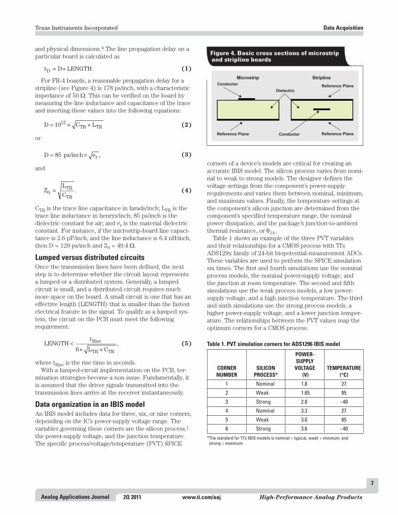
For FR-4 boards, a reasonable propagation delay for a stripline (see Figure 4) is 178 ps/inch, with a characteristic impedance of 50 W. This can be verified on the board by measuring the line inductance and capacitance of the trace and inserting those values into the following equations:
12TR TRD 10 C L= × × (2)
or
rD 85 ps/inch e ,= × (3)
and
TR0
TR
LZ .
C= (4)
CTR is the trace line capacitance in farads/inch; LTR is the trace line inductance in henrys/inch; 85 ps/inch is the dielectric constant for air; and er is the material dielectric constant. For instance, if the microstrip-board line capaci-tance is 2.6 pF/inch, and the line inductance is 6.4 nH/inch, then D = 129 ps/inch and Z0 = 49.4 W.
Lumped versus distributed circuitsOnce the transmission lines have been defined, the next step is to determine whether the circuit layout represents a lumped or a distributed system. Generally, a lumped circuit is small, and a distributed circuit requires much more space on the board. A small circuit is one that has an effective length (LENGTH) that is smaller than the fastest electrical feature in the signal. To qualify as a lumped sys-tem, the circuit on the PCB must meet the following requirement:
Rise
TR TR
tLENGTH ,
6 L C<
× × (5)
where tRise is the rise time in seconds.With a lumped-circuit implementation on the PCB, ter-
mination strategies become a non-issue. Fundamentally, it is assumed that the driver signals transmitted into the transmission lines arrive at the receiver instantaneously.
Data organization in an IBIS modelAn IBIS model includes data for three, six, or nine corners, depending on the IC’s power-supply voltage range. The variables governing these corners are the silicon process,1 the power-supply voltage, and the junction temperature. The specific process/voltage/temperature (PVT) SPICE
corners of a device’s models are critical for creating an accurate IBIS model. The silicon process varies from nomi-nal to weak to strong models. The designer defines the voltage settings from the component’s power-supply requirements and varies them between nominal, minimum, and maximum values. Finally, the temperature settings at the component’s silicon junction are determined from the component’s specified temperature range, the nominal power dissipation, and the package’s junction-to-ambient thermal resistance, or qJA.
Table 1 shows an example of the three PVT variables and their relationships for a CMOS process with TI’s ADS129x family of 24-bit biopotential-measurement ADCs. These variables are used to perform the SPICE simulation six times. The first and fourth simulations use the nominal process models, the nominal power-supply voltage, and the junction at room temperature. The second and fifth simulations use the weak process models, a low power-supply voltage, and a high junction temperature. The third and sixth simulations use the strong process models, a higher power-supply voltage, and a lower junction temper-ature. The relationships between the PVT values map the optimum corners for a CMOS process.
Reference Plane Reference Plane
Reference PlaneDielectric
Conductor
Conductor
Microstrip Stripline
Figure 4. Basic cross sections of microstrip and stripline boards
*The standard for TI’s IBIS models is nominal = typical, weak = minimum, and strong = maximum .
Table 1. PVT simulation corners for ADS1296 IBIS model
CORNERNUMBER
SILICONPROCESS*
POWER-SUPPLY
VOLTAGE (V)
TEMPERATURE(°C)
1 Nominal 1 .8 27
2 Weak 1 .65 85
3 Strong 2 .0 –40
4 Nominal 3 .3 27
5 Weak 3 .0 85
6 Strong 3 .6 –40

Texas Instruments Incorporated
8
Analog Applications JournalHigh-Performance Analog Products www.ti.com/aaj 2Q 2011
Data Acquisition
Finding and/or calculating transmitter specificationsThe required transmitter speci-fications for a signal-integrity evaluation are the out put impedance (ZT) and the rise and fall times (tRise and tFall, respectively). Figure 5 shows the package listing from the IBIS model file, ads129x.ibs,5 for TI’s ADS1296. The values that are used to produce the impedance are shown under the “[Pin]” keyword and are also within the buffer models (not shown). The rise and fall times are located in the transient por-tions of the IBIS model’s data listing.
Impedances of input and output pinsThe pin impedance of any signal consists of the package inductance and capacitance added to the model’s imped-ance. In Figure 5, the keywords “[Com ponent],” “[Manufacturer],” and “[Package]” describe a specific package, a 64-pin PBGA (ZXG). The package inductance and capacitance for specific pins can be found under the “[Pin]” keyword. For instance, at pin 5E for the signal GPIO4, the L_pin and C_pin values are given. The L_pin (pin induc-tance) and C_pin (pin capaci-tance) values for this signal and package are 1.4891 nH and 0.28001 pF, inclusive.
The second capacitance value of interest is the silicon capaci-tance, C_comp. The C_comp values can be found under the “[Model]” keyword in the model DIO_33 listing from the ads129x.ibs file (see Figure 6). C_comp in this model is the capacitance of the DIO buffer with 3.3 V applied to the power- supply pin. The “|” symbol indi-cates a comment; so the active C_comp values in this list-ing are 3.0727220e-12 F (typical), 2.3187130e-12 F (mini-mum), and 3.8529520e-12 F (maximum), from which the
ads1296zxg :: PBGA, 64 pin package
[Component] ads1296zxg
[Manufacturer] TI
|
[Package] |ZXG (PBGA) - 64 pin
| variable typ min max
R_pkg 0.084959 0.084959 0.084959
L_pkg 1.726943nH 1.173300nH 2.802300nH
C_pkg 0.203317pF 0.155540pF 0.299270pF
|
[Pin] signal_name model_name R_pin L_pin C_pin
|
1A IN8P TERM 0.080388 1.4891nH 0.16542pF
1B IN7P TERM 0.078742 1.4385nH 0.15797pF
1C IN6P TERM 0.077541 1.4231nH 0.16358pF
5E GPIO4 DIO 0.106300 2.5339nH 0.28001pF
Figure 5. IBIS model’s package listing for ADS1296, including L_pin and C_pin values
[Model] DIO_33
Model_type I/O
|Signals SCLK, DAISY_IN
|
Vinl = 0.66
Vinh = 2.64
Vmeas = 1.65
Vref = 1.65
Cref = 15pF
Rref = 50
|
| typ min max
| (nom PVT) (fast PVT) (slow PVT)
|
C_comp 3.0727220e-12 2.3187130e-12 3.8529520e-12
|C_comp (ON state) 5.2856500e-12 4.3183460e-12 6.0694320e-12
|C_comp (OFF state) 6.2160260e-12 5.1916700e-12 7.4675830e-12
|
|
| Where nom PVT is Nominal Process, 3.3V, 27C
| Fast PVT is Strong Process, 3.6V, -40C
| Slow PVT is Weak Process, 3V, 85C
Figure 6. Model DIO_33 listing of C_comp values from ads129x.ibs file
PCB designer can choose. During the design stage of the PCB transmission lines, the typical value of 3.072722 pF is an appropriate choice.

Texas Instruments Incorporated
9
Analog Applications Journal 2Q 2011 www.ti.com/aaj High-Performance Analog Products
Data Acquisition
The input and output impedances can be critical to signal transmission. The following equation defines the characteristic impedance of the IBIS model pins:
pinT R
LZ Z
C _ pin C _ comp= =
+ (6)
Output rise and fall timesAcross the industry, the convention for rise- and fall-time specifications is to use the time needed for the output signal to swing between 10% and 90% of the rail-to-rail signal, which is usually 0 to DVDD. The IBIS Open Forum’s definition for rise time is the same and was adopted because of the long tails on CMOS switching waveforms.
Output, I/O, and three-state models within the IBIS model have specifications embedded under the “[Ramp]” keyword for R_load (test load), dV/dt_r (rise time), and dV/dt_f (fall time). The range of the rise- and fall-time data is from 20 to 80% of the voltage-output signal. If the denominator of the typical dV/dt_r values is multiplied by 0.8/0.6, the rise-time value will change from a 20-to-80% swing to a 10-to-90% swing. Please note that the data represents a buffer with the resistive load, R_load. In the ads129x.ibs file, DIO_33 data assumes a 50-W load, so the data does not extend to DVDD. The resulting number from this calculation will provide an appropriate
value for tRise for the various transmission-line calculations such as fKnee, f3dB, and rising-edge lengths.
Using IBIS to design transmission linesThis article started out by discussing a PCB with mis-matched termination impedances. The IBIS model was then used to understand and find the critical elements for this transmission problem. At this point, it is only fair to show that there is a solution to this problem. Figure 7 shows the termination-correction strategy, and Figure 8 shows the corrected waveforms.
MSP430TM
ADS8326
Clock
CS
Data
Clock
CS
Data
R5 100 �
R4 100 �
R6 100 �
R2 100 �
R1 100 �
C2 220 pF
C1 220 pF
C3 220 pF
+
+
+
+
+
+
+
+
+
+
+
+
T1
T2
T3 R3 100 �
Figure 7. Termination-correction strategy
Channel 1 Clock
Channel 2 Data
Figure 8. Stable signals from termination correction

Texas Instruments Incorporated
10
Analog Applications JournalHigh-Performance Analog Products www.ti.com/aaj 2Q 2011
Data Acquisition
To design PCB transmission lines, the first step is to gather information from the product datasheet. The second step is to examine the IBIS model to find the parameters that cannot be gleaned from the datasheet—input/output impedance, rise time, and input/output capacitance. It makes sense to use the IBIS model to find key product specifications and to simulate the final design before going to the hardware stage.
ReferencesFor more information related to this article, you can down-load an Acrobat® Reader® file at www.ti.com/lit/litnumber and replace “litnumber” with the TI Lit. # for the materials listed below.
Document Title TI Lit. #1. Bonnie Baker, “The IBIS model: A conduit
into signal-integrity analysis, Part 1,” Analog Applications Journal (4Q 2010) . . . . . slyt390
2. Bonnie C. Baker, “The IBIS model, Part 2: Determining the total quality of an IBIS model,” Analog Applications Journal (1Q 2011) . . . . . . . . . . . . . . . . . . . . . . . . . . . . . . . . slyt400
Document Title TI Lit. #3. Shankar Balasubramaniam, Ramzi Ammar,
Ernest Cox, Steve Blozis, and Jose M. Soltero, “Basic design considerations for backplanes,” Application Report. . . . . . . . . . . . . . . . . . . . . . . . .szza016
4. Howard W. Johnson and Martin Graham, High-Speed Digital Design: A Handbook of Black Magic. Englewood Cliffs, NJ: Prentice Hall, 1993. —
5. ads129x.ibs IBIS Model [Online]. Available: http://www.ti.com/litv/zip/sbam021b —
6. “Using IBIS models for timing analysis,” Application Report. . . . . . . . . . . . . . . . . . . . . . . . .spra839
7. Roy Leventhal and Lynne Green, Semiconductor Modeling for Simulating Signal, Power, and Electromagnetic Integrity. New York: Springer Science+Business Media, LLC, 2006. —
Related Web sitesdataconverter.ti.comwww.ti.com/sc/device/ADS1296www.ti.com/sc/device/ADS8326

11
Analog Applications Journal
Texas Instruments Incorporated
2Q 2011 www.ti.com/aaj High-Performance Analog Products
Implementation of microprocessor- controlled, wide-input-voltage, SMBus smart battery charger
With the increasing popularity of lithium-ion chemistries in all types of electronics designs, innovative solutions for charging these batteries are becoming essential. For the utmost in system flexibility, a microprocessor can be used to control all aspects of battery charging, including unique charging algorithms to increase the charging rate and life-time of the cells. This method also allows for higher-voltage battery-pack implementations.
This article describes using a microprocessor to control the power-stage board of a wide-input-voltage DC/DC con-troller. This solution can support an input voltage of up to 55 V; a battery-charging voltage ranging from 5 to 51 V; and up to 10 A of output current in most cases. Both the hard-ware and software discussed in this article have been devel-oped and tested by Texas Instruments (TI) applications staff to allow customers to quickly prototype the solution.
For ease of development, the battery charger is split into two separate boards: the microprocessor controller board and the DC/DC-converter power-stage board (see Figure 1). The positive and negative battery terminals are connected to the power-stage board, while the system-management bus (SMBus) communication lines are con-nected to the microprocessor board. The smart battery sends the desired charging voltage and current information to the microprocessor, which then sends two pulse-width-modulated (PWM) signals to the DC/DC-converter power-stage board to set the actual output voltage and current.
To permit the use of a standard wide-input-voltage DC/DC converter, the power-stage board is designed with a
Power Management
By Keith KellerAnalog Field Applications/Power Management
MSP430™Controller
Board
PWM
SMBus
DC/DC-Converter
Power-StageBoard
SDA
SCL
Power SmartBatterySystem
bqFuel-Gauge
Chipset
VCC
Figure 1. High-level system block diagram of wide-input-voltage smart battery charger
special feedback circuit (see Figure 2) to properly control the charging of the battery. The charging sequence that the microprocessor follows is to first limit the charge current until the battery voltage approaches its specified maximum voltage. When the maximum voltage is reached, the charge voltage is held constant, allowing the charge current to taper down until the battery is deemed fully charged. At this point the PWM output signals are shut off.
The initial current-limiting charge rate could have two current levels. When a battery has been overly discharged, a fractional charge rate is used until the battery voltage is at a safe enough level to accept the normal charge rate.
In the feedback circuit shown in Figure 2, U3:B com-pares the PWM-current reference voltage (I_PWM1) to the measured current (ISNS1) being delivered to the battery. If the PWM reference voltage is higher than the measured current, the output of the amplifier is high. If the refer-ence voltage is lower, the output of the amplifier is low.
A resistor divider (R30 and R34) is used to measure the output voltage at the VBATT1 input to U3:A. This voltage is compared to the PWM-output reference voltage (V_PWM1). If this reference voltage is higher, the output of the amplifier is high. If the reference voltage is lower, the output of the amplifier is low. The maximum output voltage is dictated by
OUT(max)VBATT1
V .R34 (R34 R30)
=× +

Texas Instruments Incorporated
12
Analog Applications JournalHigh-Performance Analog Products www.ti.com/aaj 2Q 2011
Power Management
4OUT 2OUT
14 7
1
12 6
2
4
13 5
311
U3:DTLV274PW
U3:BTLV274PW
U3:ATLV274PW
R26
10 k�
R102
20 k�R23
10 k�
R21
10 k�R22
51.1 �
C151 µF
C161 µF
C211 µF
C11310 µF
C200.1 µF
C170.047 µF
C190.01 µF
R16
10 k�
R28
1 k�R29
1 k�
R19
1 k�
R31
10 k�
R17
10 k�
R30
15 k�
R20
100 k�
R32
10 k�
R24
1 M�
R33
1 M�R34
1 k�
D1BAT54A
R15
10 k�
To DC/DCConverter
–
+–
+
–
+
VDD
ISNS1
VBATT1
I_PWM1
V_PWM1
VBIAS
VBIAS
Figure 2. Constant-current/voltage-feedback circuitry to properly charge a battery
Q7
10 to 100 V
Q9
Q12
InputOvervoltageProtection
ReverseVoltageProtection
1
2
J9
GND
Q11
Q13
Q18
D26.2 V
D36.2 V
C2347 µF
R39
100 k�
R37
10 k�
R40
10 k�
R41
10 k�
R44
10 k�
R42
3.01 k�
R43
3.01 k�
C240.1 µF
C2522 pF
1
2
+
J10
SD1
SD2
GND
10 to 58 V1
2
J8
VIN
VIN_2Q8
Q10
D456 V
C224.7 µF
R38
100 k�
Figure 3. Overvoltage and reverse-polarity protection circuitry

Texas Instruments Incorporated
13
Analog Applications Journal 2Q 2011 www.ti.com/aaj High-Performance Analog Products
Power Management
The D1 diodes combine the outputs of the two amplifiers with a logical OR. The voltage that is lowest is fed into an inverting amplifier (U3:D) that makes the error signal’s polarity correct for the DC/DC controller (in this case TI’s TPS40170). The basic operation is that the controller tries to send a set current; and, if the load can accept this current, the controller regulates to that current level. If the load cannot accept the full amount of current, the voltage begins to rise and eventually reaches VOUT(max). When this happens, the voltage loop takes over and regulates the output voltage.
To enhance the safety of the solution, also included on the power-stage board is protection circuitry both for overvoltage conditions (up to 100 V) and for reverse-voltage connections (where the positive and negative leads are swapped). This circuitry is shown in Figure 3.
Reverse-voltage protection is provided by MOSFETs Q7 and Q9 along with D2 in case the input voltage is connected backwards. This does not allow a negative voltage to be applied to the system. Input-overvoltage protection is provided by MOSFETs Q8 and Q10. Zener diode D4 sets the voltage that the circuit starts to clamp. Once the Zener voltage is exceeded, the gate-to-source voltage of the FETs starts to drop. This causes the FETs to operate in the linear region and allows the microprocessor to continue to be powered. At the same time, the DC/DC converters are turned off, with signals SD1 and SD2 being pulled to ground.
The software implementation is equally as important as the hardware. The abbreviated software flowchart is shown in Figure 4. The microprocessor interrogates the battery via SMBus for its desired charging voltage and current. After confirming the values, it sets two PWM outputs accordingly to regulate the output voltage and current going to the battery. If at any time the battery issues a charging alarm, the PWM outputs will shut off. Addition-ally, the PWM outputs will shut off as soon as the battery’s state of charge reaches 100% or the fully charged bit is set.
Safety is of utmost concern during battery charging. Any solution should allow for several levels of protection. The first level of protection is the smart battery itself with its internal protection MOSFETs. During charging, the micro-processor should communicate with the battery on a regu-lar basis (every 2 seconds is good) and monitor for any safety flags in the “Battery Status” register. The flag bits that require action are the overcharge alarm (OCA), terminate-charge alarm (TCA), overtemperature alarm (OTA), and fully charged (FC) condition. The micro proc es-sor’s onboard analog-to-digital converter can be used as a secondary check for an overvoltage or overcurrent event.
ConclusionA fully programmable, wide-input-voltage battery charger can be designed by using a microprocessor in conjunction with a wide-input-voltage DC/DC controller. This article
has presented a solution that uses TI’s low-power MSP430F5510 microprocessor together with the TPS40170 DC/DC controller, a configuration that can support an input voltage of up to 55 V. The special feed-back network developed by TI applications staff for proper battery charging has been described. Additionally, a novel solution was shown for overvoltage protection, and reverse-voltage protection was discussed. The software required to communicate to a smart battery via SMBus communications protocol can be downloaded from a link in Reference 1, which is an application report. Detailed information on the SMBus smart battery charger is also available in Reference 1.
ReferenceFor more information related to this article, you can down-load an Acrobat® Reader® file at www.ti.com/lit/litnumber and replace “litnumber” with the TI Lit. # for the materials listed below.
Document Title TI Lit. #1. Abhishek A. Joshi and Keith J. Keller, “Wide-
Vin battery charger using SMBus communica- tion interface between MSP430™ MCUs and bq fuel gauges,” Application Report. . . . . . . . . . .slaa476
Related Web sitespower.ti.comwww.ti.com/sc/device/MSP430F5510www.ti.com/sc/device/TPS40170
Interrogate battery forcharging voltage,charging current, stateof charge (0 to 100%),and battery status(SMBus slave mode)
Battery status:Is there an error
condition?
Halt PWM outputsto stop charging
Adjust PWM todeliver powerrequested
No
No
Yes
Yes
Is batteryfully charged?
Wait a fewseconds
StartInitialize MSP430™(SMBus master mode)
Stop
Figure 4. Abbreviated overview of software flowchart

Analog Applications JournalHigh-Performance Analog Products www.ti.com/aaj 2Q 2011
Texas Instruments Incorporated
14
Benefits of a coupled-inductor SEPIC converter
The single-ended primary-inductor converter (SEPIC) is capable of operating from an input voltage that is greater or less than the regulated output voltage. Aside from being able to function as both a buck and boost converter, the SEPIC also has minimal active components, a simple con-troller, and clamped switching waveforms that provide low- noise operation. The SEPIC is often identified by its use of two magnetic windings. These windings can be wound on a common core, as in the case of a coupled dual-winding inductor, or they can be the separate windings of two uncoupled inductors. Designers are often unsure of which approach is best and whether there is any real difference between the two. This article looks at each approach and discusses the impact each has on a practical SEPIC design.
Circuit operationFigure 1 shows the basic SEPIC with a coupled inductor. When the FET (Q1) turns on, the input voltage is applied across the primary winding. Since the winding ratio is 1:1, the secondary winding is also imposed with a voltage equal to the input voltage; but, because of the polarity of the windings, the anode of the rectifier (D1) is pulled neg-ative and reverse-biased. With the rectifier biased off, the output capacitor is required to support the load during this ON time, which forces the AC capacitor (CAC) to be charged to the input voltage. While Q1 is on, current flow in both windings is through Q1 to ground, with the sec-ondary current flowing through the AC capacitor. The total FET current during the ON time is the sum of the input current and the output secondary current.
When the FET turns off, the voltage on the windings reverses polarity to maintain current flow. The secondary-winding voltage is now clamped to the output voltage when the rectifier conducts to supply current to the output. Through transformer action, this clamps the output voltage across the primary winding. The voltage on the drain of the FET is clamped to the input voltage plus the output voltage. Current flow during the FET OFF time for both windings is through D1 to the output, with the primary current flowing through the AC capacitor.
Balancing volt-microsecondsThe circuit operates similarly when the coupled inductor is replaced with two uncoupled inductors. For the circuit to operate properly, volt-microsecond balance must be maintained across each magnetic core. That is, for the two uncoupled inductors, the products of each inductor’s volt-age and time must be equal in magnitude and opposite in polarity during the FET ON and OFF times. It can be
algebraically shown that the AC capacitor voltage for uncoupled inductors is also charged to the input voltage. See the Appendix for details. The output-side inductor is clamped to the output voltage during the FET OFF time, as was the secondary winding of the coupled inductor. During the FET ON time, the AC capacitor imposes a poten tial equal to the input voltage but opposite in polarity across the inductor. With defined voltages clamped across the inductor for each interval, balancing the volt-microseconds determines the duty cycle (D). This is simply
OUT
OUT IN
VD ,
V V=
+
for continuous-conduction-mode (CCM) operation. The voltage imposed across the input-side inductor is equal to the input voltage when the FET is on. When the FET is off, volt-microsecond balance is maintained by clamping VOUT across it. It is easy to remember that when the FET is on, the input voltage is applied across both inductors; and when the FET is off, the output voltage is imposed across both. The voltage and current waveforms of the two uncoupled-inductor SEPICs are quite similar to those of the coupled-inductor version, so much so that it would be difficult to tell them apart.
Two versus one?If there is little difference in circuit operation between the SEPIC types, does it matter which one to use? A coupled inductor is often selected due to its reduced component count, better integration, and lower inductance require-ment compared to using two single inductors. However,
By John BettenApplications Engineer
Power Management
CIN
CAC
D1+
L1VIN
VOUT
COUT
Q1
Figure 1. The basic coupled-inductor SEPIC

Texas Instruments Incorporated
15
Analog Applications Journal 2Q 2011 www.ti.com/aaj High-Performance Analog Products
Power Management
the limited selection of higher-power off-the-shelf coupled inductors poses a problem for power-supply designers. If they choose to design their own inductors, they must specify all pertinent electrical parameters as well as deal with longer lead times. Coupled-inductor SEPICs can bene-fit from leakage inductance, which reduces AC current losses.1 Coupled inductors must have a 1:1 turns ratio for volt-microsecond balance. Choosing to use two separate uncoupled inductors typically offers a much broader selec-tion of off-the-shelf components. Since the currents and even the inductances for each inductor are not required to be identical, different component sizes can be selected for each, providing greater flexibility.
Equations 1 through 3 show the calculations for induc-tance for both coupled and uncoupled inductors.
2 2IN(max) min
Coupled
s OUT(min) min
V dL
12 f P 1 d
×=
− η × × × + × η
(1)
2min IN(max)
1s OUT(min)
d VL
2 f P
× × η=
× × (2)
2min OUT
2s OUT(min)
(1 d ) VL
2 f P
− ×=
× × (3)
The equations determine the minimum inductance neces-sary for CCM operation at maximum input voltage and minimum load. Comparing these equations at 50% duty-cycle operation (which occurs when VIN equals VOUT) and unity efficiency, the value calculated for the coupled inductor in Equation 1 is twice that of the uncoupled inductors. Since the converter will certainly have losses, and most input voltage sources vary quite a bit, this simpli-fied inductance generalization is usually false; but it is often adequate for all but extreme cases. It usually means that the converter will enter discontinuous-conduction-mode (DCM) operation slightly sooner (or later) than expected, which in most cases is still acceptable. As previ-ously mentioned, with uncoupled inductors it is not neces-sary that the output-side inductor be the same value as the input-side inductor, as is often assumed; but this can certainly be done for simplicity’s sake. The output-side inductor’s value can simply be determined by scaling the
input-side inductor by VOUT/VIN. The benefit of using a lower-value output-side inductor is that it is typically smaller and costs less.
Example designsThe specifications shown in Table 1 are the basis for a design comparison. The first design uses a coupled induc-tor, and the second uses two uncoupled inductors.
The design using a coupled inductor is typical of an automotive input-voltage range with an output power of 64 W. Equation 1 determines that the coupled inductor requires an inductance of 12 µH, with a combined current rating of 13 A (based on IIN + IOUT). This design poses a particular challenge because of the limited selection of off-the-shelf inductors. Therefore, a custom inductor from Renco was specified and designed. This inductor was wound on a split bobbin to intentionally introduce leakage inductance to minimize circulating AC currents that can induce losses. These losses are due to the AC capacitor’s ripple voltage being imposed across the leakage induc-tance. For designs of lower power, coupled inductors from Coilcraft (MSS1278 series) and Coiltronics (DRQ74/127 series) offer good off-the-shelf alternatives.
For the design with uncoupled inductors, a 33-µH Coilcraft SER2918 was used for L1, and a 22-µH Coiltronics HC9 was used for L2. Each was chosen based on winding resistance, current rating, and size. When selecting the inductors, the designer must take care to also consider core and AC winding losses. These losses reduce the inductor’s allowable DC current, but not all vendors provide adequate information to calculate this. Failure to properly calculate this could greatly increase core temperature beyond the typical 40°C rise. It could also decrease efficiency and hasten premature failure.
Table 1. Prototype SEPIC electrical specifications
PARAMETER SPECIFICATION
Input voltage 8 to 32 V
Output voltage 16 V
Maximum output current 4 A
Ripple 1%
Minimum efficiency (maximum load) 91%

Texas Instruments Incorporated
16
Analog Applications JournalHigh-Performance Analog Products www.ti.com/aaj 2Q 2011
Power Management
Figure 2 shows a schematic of the prototype SEPIC with a coupled inductor. To implement the uncoupled inductors in the design, the coupled inductor was simply replaced with two inductors on the same PWB. Figure 3 shows both prototype circuits. In Figure 3b, L1 occupies the space of the coupled inductor, and L2 is in the upper right corner.
As expected, both circuits operated in a nearly identical fashion, with the switching voltage and current waveforms being essentially the same. But there were several key dif-ferences in performance. While the control loop for the coupled-inductor design was quite benign, the design with uncoupled inductors was initially unstable. Measurement
V =8 to 32 V
IN
V =16 V at 4 A
OUT
R2
20 k�D1
6.8 V
C13270 pF
C18100 pF
R14
453 �
R3
20 k�
R11
10 k� R12
10 k�
11
PwPd
VDD
VBP
GDRV
ISNS
GND
RC
SS
DIS/
COMP
FB
EN
R5
210 k�
R7 1 k�
R63.9 �
U1TPS40210
D26.8 V
C140.22 µF
C80.33 µF
C151 µF
3.3 µF50 V
L112 µH
C1220 µF50 V
C23.3 µF50 V
C33.3 µF50 V
680 µF25 V
C1210 µF25 V
C17150 pFC16
0.15 µF
Q1Q3
Q4IPP084N06L3G
1
3
8
7
D4
D3MBR20L60CT
1 11
2 125 7
6 84X
3X
T150:1Q2
R4
100 k�
R10010 �
R1
10 �
R80.39 �
UVLO10
9
8
7
6
1
2
3
4
5
+
+
J11
2
1
2
J2
Figure 2. SEPIC (16 V at 4 A) with coupled inductor
Figure 3. SEPIC prototypes
(a) With coupled inductor (b) With uncoupled inductors

Texas Instruments Incorporated
17
Analog Applications Journal 2Q 2011 www.ti.com/aaj High-Performance Analog Products
Power Management
of the loop gain determined that a high-Q, low- frequency resonance was the culprit, requiring the addition of an R/C damping filter in parallel with the AC capacitor. The resonant frequency, while greatly simplified, appeared to be approximately
AC
1 .2 C (L1 L2)π × +
The SEPIC circuit has quite complex control-loop characteristics, necessitating the use of mathemati-cal tools for detailed analysis because the analytical results are often difficult to interpret. Adding this R/C damping filter(220 µF/2 W) increases the cost, circuit area, and losses. This is in addition to the extra 10% area required for two uncoupled induc-tors versus a single coupled inductor.
Figure 4 shows the measured efficiency for both circuits. It can be seen that there is an across-the-board boost in efficiency of up to 0.5% for the coupled-inductor design. This is likely due to lower overall core losses in the coupled-inductor design, since its DC wiring losses were actually higher than those in the design with uncoupled inductors. L2 uses a powdered-iron core material, which tends to have higher losses than the ferrite material used for L1 and the custom Renco coupled inductor.2 While ferrite material for L2 could have been used, it would have resulted in a larger area.
ConclusionThe SEPIC can be successfully implemented with either a coupled inductor or two uncoupled inductors. Improved efficiency, reduced circuit area, and more benign control-loop characteristics are benefits realized in the prototype hardware when a properly wound custom coupled induc-tor is used. While custom components are less desirable than off-the-shelf parts, many coupled inductors are readily available, albeit in smaller sizes. If time to market is critical, uncoupled inductors provide greater flexibility to the designer.
References1. John Betten. (May 27, 2010). SEPIC converter benefits
from leakage inductance. PowerPulse.Net Design Features [Online]. Available: http://www.powerpulse.net/techPaper.php?paperID=153
2. Robert Kollman. (July 13, 2009). Power tip: Don’t get burned by inductor core losses. EE Times Power Management DesignLine [Online]. Available: http://www.eetimes.com/design/power-management-design /4012507/Power-Tip-Don-t-get-burned-by-inductor-core-losses
Related Web sitespower.ti.comwww.ti.com/sc/device/TPS40210
94
93
92
91
90
89
88
870.0 0.5 1.0 2.0 3.0 4.01.5 2.5 3.5 4.5
Output Current (A)E
ffic
ien
cy
(%
)
VIN = 12 VCoupledUncoupled
V = 24 VIN
CoupledUncoupled
Figure 4. Both coupled and uncoupled inductors achieve good efficiency
Appendix: Algebraic proof for VIN = VCap with uncoupled inductorsThe following two equations are used to balance the volt-microseconds for L1 and L2:
IN Cap OUT IND V (1 D)(V V V ) (for L1)× = − + −
OUT Cap(1 D) V D V (for L2)− × = ×
CapOUT
V Dor V
1 D
×=
−
The following sequence uses substitution and simplification techniques with these two equations to obtain the result:
CapIN Cap IN
V DD V (1 D) V V
1 D
× × = − × + −
−
IN Cap Cap IND V (1 D) V V D (1 D) V× = − × + × − − ×
IN Cap Cap IN IND V (1 D) V V D V D V× = − × + × − + ×
IN Cap CapV (1 D) V V D= − × + ×
IN Cap Cap CapV V D V V D= − × + ×
IN CapV V=

Analog Applications JournalHigh-Performance Analog Products www.ti.com/aaj 2Q 2011
Texas Instruments Incorporated
18
IQ: What it is, what it isn’t, and how to use it
IntroductionA device’s quiescent current, or IQ, is an important yet often misused parameter for low-power, energy-efficient designs. In many battery-powered applications, the cur-rent drawn from the battery in a standby condition with light or no load defines the total run time of the system. In integrated switch converters, the IQ is only one portion of this battery current. This article defines IQ and how it is measured, explains what IQ is not and how it should not be used, and gives design considerations on how to use IQ while avoiding common measurement errors. This article applies to any of the Texas Instruments (TI) TPS61xxx, TPS62xxx, TPS63xxx, or TPS650xx devices.
What IQ isUnless otherwise noted in the datasheet for a part, IQ is defined as the current drawn by the IC in a no-load and nonswitching but enabled condition. “No load” means that no current leaves the IC to the output. Typically, this would be current leaving via the SW pin on buck converters or via the VOUT pin on boost converters. All of the IQ simply travels inside the IC to ground. “Nonswitching” means that no power switch in the IC is on (closed). This includes the main or control switch as well as the synchronous rectifier if both are integrated into the IC. In other words, the IC is in a high-impedance condition with a power stage that is completely disconnected from the output (except for inte-grated MOSFET body diodes on some devices that cannot be turned off). “Enabled” means that the IC is turned on via its EN pin and is not in a UVLO or other shutdown condition. IQ measures operating current, not shutdown current, so the device must be on. Lastly, IQ is meaningful only in power-save mode, so if this mode is an option for the particular device, it must be enabled. If the device runs in pulse-width-modulation (PWM) mode, then the input current to the power stage and switching losses more than dwarfs the miniscule amount of current, the IQ, required to run the device.
IQ fundamentally comes from two inputs: VIN and VOUT. The datasheet lists whether the IQ comes from either or both pins. Figure 1 shows the IQ specification from the datasheet for the TI TPS61220/21/22,1 which are boost converters that draw their IQ from both VIN and VOUT. Typically, a buck converter draws IQ only from its input, while a boost converter or buck-boost converter draws IQ from both the input and the output.
IQ measures the current required to operate the device’s basic functionality, which includes powering things like the internal precision reference voltage, an oscillator, a thermal shutdown or UVLO circuit, the device’s state machine or other logic gates, etc. IQ does not include any input current to the power stage or gate drivers, as it is measured in a nonswitching condition where these currents are zero. The reason for measuring IQ in this condition is that it is solely dependent on the IC, whereas the power-stage input cur-rent and gate-drive current are dependent on the selected external components, which in most cases dictate how often the IC switches in its power-save mode. Thus, IQ is an IC measurement, whereas including the other two cur-rents is a system measurement. TI does not control and cannot guarantee such a system measurement but does control and can specify an IC measurement. In fact, TI guarantees the IQ specification and, for devices whose datasheets specify a maximum value for the IQ, tests it on each and every device that is produced. This is done by enabling the device, setting it to the test conditions speci-fied in its datasheet, and then artificially raising (with externally applied voltages) the output voltage, FB pin, and any other pin voltages high enough to cause the IC not to switch. With no load and power-save mode enabled (if available), the input current to the IC becomes the IQ.
What IQ isn’tIQ is not the no-load input current. As previously men-tioned, the IQ is simply the “overhead” current required to operate the IC’s basic functionality. It does not include the
By Chris GlaserApplications Engineer
Power Management
DC/DC STAGEPARAMETER TEST CONDITIONS MIN TYP MAX UNIT
VIN 0.5 0.9 µAQuiescentIQ IO = 0 mA, VEN = VIN = 1.2 V, VOUT = 3.3 Vcurrent VOUT 5 7.5 µA
Figure 1. IQ specification from TPS61220/21/22 datasheet

Texas Instruments Incorporated
19
Analog Applications Journal 2Q 2011 www.ti.com/aaj High-Performance Analog Products
Power Management
input current into the power stage (current that is actually transferred to the output) or current required to operate the gate drivers. Even at no load, the device still switches to keep the output regulated. Some losses always exist at the output, such as loss from the voltage divider used to set the output voltage; leakage current into the load or through the output capacitor; pull-up resis-tors; etc. Because these losses cause voltage decay at the output capacitor, the IC must switch every so often to replenish the power lost. So, a no-load input-current measure-ment violates the requirements that the IC must be in a nonswitching condition and that no current may leave the IC to recharge VOUT. As an example, Figure 2 shows no-load operation for the TPS61220 boost converter, with an input voltage of 1.2 V and an output voltage of 3.3 V. The IC switches approxi-mately every 1.75 ms to regulate the output voltage. This period depends on VIN, VOUT, and the external components and affects how much average input current is drawn. During phase #1, the IC is switching—either the high-side MOSFET or the synchronous rectifying MOSFET is on. The input current is dominated by the current into the power stage, which averages about 70 mA (half of the peak current in the inductor).
Figure 3 shows an enlarged view of phase #1. Once the output voltage drops below the threshold, the TPS61220 begins a switching pulse by turning the control MOSFET on. The SW pin goes low, causing the inductor current to ramp up. It then turns off the control MOSFET and turns on the rectifying MOSFET, allowing current to flow to the output. The output voltage increases as this energy is transferred into the output capacitor. When the inductor cur-rent reaches zero, all the energy has been delivered to the output; so the rectifying MOSFET turns off, and the IC goes into a sleep mode (phase #2). At this point, both MOSFETs are off (open), so the SW pin is in a state of high impedance. The inductor and parasitic capacitances on that pin ring until it reaches its DC value, which equals the input voltage.
During phase #2, the IC is high impedance, and the out-put voltage drops due to leakage at the output. Because the IC is not switching, the current consumed by the IC during this time is the IQ. Phases #1 and #2 define a switch ing period over which the average input current is calculated. Due to the high input current during the
switching time (phase #1), the average input current over this time must be higher than the IC’s IQ. However, because the duration of phase #1 is very short, the average input current is usually only slightly greater than the input cur-rent that is due to the IQ.
To address this difference between the IQ and the no-load input current, the datasheets of some ICs have typical specifications for the no-load input current in the electri-cal characteristics table. Others have graphs that show the
Phase #1
Phase #2
Switch Node(1 V/div)
V (AC-Coupled, 10 mV/div)OUT
I (100 mA/div)L
Time (500 µs/div)
1
2
4
V = 1.2 V
V = 3.3 VIN
OUT
Figure 2. No-load operation of TPS61220
Phase #2
Phase #1
Switch Node(1 V/div)
V (AC-Coupled, 10 mV/div)OUT
I (100 mA/div)L
Time (500 ns/div)
1
2
4
V = 1.2 V
V = 3.3 VIN
OUT
Figure 3. Switching pulse of TPS61220 during no-load operation

Texas Instruments Incorporated
20
Analog Applications JournalHigh-Performance Analog Products www.ti.com/aaj 2Q 2011
Power Management
no-load input current for a particular circuit. Figure 4 shows such a graph from the TPS61220/21/22 datasheet.1 Alternatively, Figure 5 shows the IQ specification in an electrical characteristics table. This table is taken from the datasheet for the TI TPS62120/22,2 which are high-efficiency buck converters. The typical specification of 13 µA is valid only for the specific test conditions stated. For both the TPS61220 and TPS62120, note that the no-load input current is higher than the IC’s IQ. Figure 4 shows that the no-load input current to the TPS61221 boost converter is 20 µA with a VIN of 1.2 V and a VOUT of 3.3 V. This is much higher than the IQ in Figure 1 of 5 µA at VOUT and 0.5 µA at VIN with the same test conditions. This difference is explained later in this article under item #3 of “Design considera tions.”
How to use IQKnowing the IQ assists the designer in com paring the low-power performance of different ICs. However, an IC’s IQ is only part of the system’s input current, which is affected
PARAMETER TEST CONDITIONS MIN TYP MAX UNITSUPPLY
IOUT = 0mA, Device not switching, EN = VIN, 11 18 µAregulator sleepsIQ Quiescent current
IOUT = 0mA, Device switching, VIN = 8 V, VOUT = 13 µA1.8V
Figure 5. No-load input-current specification from TPS62120/22 datasheet
80
70
60
50
40
30
20
10
00.7 1.7 2.7 3.7 4.7
Input Voltage, V (V)IN
Device Enabled
Inp
ut
Cu
rre
nt,
I( µ
A)
INTPS61222, V = 5 VOUT
TPS61221, V = 3.3 VOUT
TPS61220, V = 1.8 VOUT
Figure 4. Graph of no-load input current from TPS61220/21/22 datasheet
by three things: each IC’s internal design (its IQ), the external components around each IC, and the overall sys-tem configuration. Because the input current is a combi-nation of these three items, IQ losses may or may not be the dominant loss for a particular system and may or may not be the determining factor in the battery’s run time.
If the end application truly operates the IC at no output load, then an IC with lower IQ typically has lower no-load input current, which results in longer battery run time. This assumes that both ICs have a power-save mode and that it is enabled. However, power-save modes can behave differently among different ICs, resulting in vastly differ-ent no-load input currents.
If the application does not run at no load but instead runs in a “standby” or “hibernate” mode in which the proc-essor or another load still draws some current, then the usefulness of IQ quickly decreases. To demonstrate, con-sider the TPS62120 powering TI’s MSP430™ and other circuitry that altogether consume 100 µA at 2 V. With an 8-V input, the TPS62120 is running at 60% efficiency (see

Texas Instruments Incorporated
21
Analog Applications Journal 2Q 2011 www.ti.com/aaj High-Performance Analog Products
Power Management
Figure 62), resulting in an input current of
2 V 100 A42 A.
0.6 8 V× µ
= µ×
This input current includes the IQ (11 µA), which is a very significant portion of the total input current (about 26%). If, however, the standby load increases to 1 mA, the input current at 8 V is
2 V 1 mA313 A.
0.8 8 V×
= µ×
Now the 11 µA of IQ is not significant at all (about 3.5%). To accurately estimate the input current in a system’s standby mode, the load current drawn must be known. Simply using the IQ in place of this light-load input current does not accurately estimate the battery current drawn.
Any efficiency graph in a datasheet indicates the total circuit efficiency and includes the IQ losses. Therefore, the IQ losses should not be added to the losses given in the graphs.
Design considerationsNumerous errors can be made when IQ values are mea-sured or taken from a datasheet. The following five con-siderations will help the designer avoid these errors.
1. The IQ of an IC cannot be changed. Nothing can be done from outside the IC that affects the IQ. The IQ does vary over input voltage and temperature, but the behav-ior of the IC’s internal circuitry sets this variation. If the IC is operated in forced PWM mode or a load is attached to the output, then the IQ is no longer applicable to the circuit, and the input current becomes applicable
instead. Many things can be done in an application that affect the input current, but not the IQ.
2. Specified operating conditions need to be con sidered. IQ is specified only for an IC’s recommend-ed operating conditions and for certain test conditions, specifically an input voltage and an output voltage. For any IC, the specified IQ is not guaranteed when the input voltage is above the recommended maximum (but less than the absolute maximum) or when the input voltage is below the recommended minimum (but above the UVLO level). For a buck converter, IQ is valid only when the input voltage is greater than the output voltage and when the device is not in dropout (100% mode). For a boost converter, the input voltage must be less than the output voltage so that the IC is not in down mode.
3. Input current is often linked to the output. The majority of the IQ for a synchronous boost usually comes from the output voltage. Since this power must ulti-mately come from the input, the input current in a no-load condition is substantially higher than the IQ because the input current for a boost converter must be greater than its output current. Consider the TPS61220 boost-ing from 1.2 V to 3.3 V. With an IQ of 5 µA at VOUT and 0.5 µA at VIN, and assuming 100% conversion efficiency, the input current from the IQ alone is
3.3 V 5 A0.5 A 14.25 A.
1.2 V× µ
+ µ = µ
The circuit actually draws about 20 µA of input current at no load (as shown in Figure 4) simply because of non-IQ losses such as switching losses and gate-drive
100
90
80
70
60
50
40
300.1 1 10 100
Output Current, I (mA)OUT
Eff
icie
nc
y (
%)
V = 2 V
L = 18 µH
LPS3015
C = 4.7 µF
OUT
OUT
V = 6 VIN
V =IN 4 V
V =IN 10 V
V =IN 8 V
V =IN 15 VV =IN 12 V
V =IN 2.5 V
Figure 6. Efficiency graph for TPS62120

Texas Instruments Incorporated
22
Analog Applications JournalHigh-Performance Analog Products www.ti.com/aaj 2Q 2011
Power Management
losses. The important point is that this 20 µA of input current is much greater than the IC’s IQ of 5.5 µA because the TPS61220 is a boost converter that draws most of its IQ from the output voltage.
4. Look for all possible input-current paths. When measuring the IQ on an evaluation module (EVM) or other board, the designer should ensure that the input current to the board is going entirely into the IC and not to other places on the board. Leakages from capaci-tors or other devices, even if the devices are disabled, may be significant due to the small IQ values and may affect the input current to the board. In addition, on some EVMs and most end-equipment boards, the input voltage or output voltage is routed to pull-up resistors, indicator LEDs, or other devices that may sink current under some conditions. Obviously, this current draw is not part of the IC’s IQ. Finally, the IC’s IQ is of no impor-tance as a system parameter, since total input current is actually what is needed; and that is easily measured at the required test conditions.
5. Measurement techniques can make a big difference. To get accurate measurements of the low-power input current or the efficiency in power-save mode, it is critical to follow the test setup detailed in Reference 3.
ConclusionIQ is an important IC design parameter in modern low-power DC/DC converters and partially defines the current drawn from the battery in light-load conditions. The IQ is
not the IC’s no-load input current, as the IC consumes the IQ current only in a no-load, enabled, and nonswitching condition. Due to leakage at the output, the IC must switch to keep the output voltage regulated. Instead of using an IC’s IQ as an estimate of the battery’s current draw, the designer should measure and use the no-load input current to the system. An even better way to esti-mate the battery’s current draw is to define the system’s load when the system is in low-power mode and then measure the battery’s actual current draw at this operating point. Doing this instead of simply using IQ allows accurate prediction of battery run times.
ReferencesFor more information related to this article, you can down-load an Acrobat® Reader® file at www.ti.com/lit/litnumber and replace “litnumber” with the TI Lit. # for the materials listed below.
Document Title TI Lit. #1. “Low input voltage step-up converter in 6 pin
SC-70 package,” TPS61220/21/22 Datasheet. . . .slvs7762. “15V, 75mA high efficient buck converter,”
TPS62120/22 Datasheet . . . . . . . . . . . . . . . . . . . .slvsad53. Jatan Naik, “Performing accurate PFM mode
efficiency measurements,” Application Report . .slva236
Related Web sitespower.ti.comwww.ti.com/sc/device/TPS61220www.ti.com/sc/device/TPS62120

23
Analog Applications Journal
Texas Instruments Incorporated
2Q 2011 www.ti.com/aaj High-Performance Analog Products
Backlighting the tablet PC
IntroductionThe tablet PC market is expected to grow from just over 50 million units this year to over 200 million units by 2016. There is still no standard architecture for the tablet PCs. For example, some models are powered by single Li-ion batteries while others use dual Li-ion batteries. Regardless of how many batteries are used, all of the tablet PC manu-facturers want to maximize battery life. The display’s back-light can be one of the most power-consuming systems in the tablet. With display sizes ranging from 7 to 10 inches, the number of backlight LEDs in recently released tablet PCs ranges from 20 to 36. This article gives guidance on how to select the optimal WLED driver and LED-string configuration to meet tablet application requirements without sacrificing efficiency and therefore battery life.
Requirements for tablet backlightingSimilar to a notebook or netbook, a tablet backlight-driver application is based on a DC/DC converter and a resistive path to ground for the LEDs. This type of application typi-cally has the following requirements:
1. Low EMI in the RF range
2. No visible flicker during dimming
3. Minimal audible noise caused by piezoelectric buzzing of the ceramic output capacitor
4. Consistent brightness across the display
5. High dimming ratio
6. Highest efficiency for maximum battery life
Meeting the first requirement, low EMI in the RF range, is relatively easy. Power-supply designers have been achiev-ing this for years with such techniques as setting the switching frequency and subsequent harmonics outside the RF range, using shielded inductors, and designing the PCB with minimal length but with wide traces where appropriate. Some driver ICs have integrated MOSFET gate-drive circuits with tiered rise times to reduce noise emissions in the RF range.
The type of dimming strongly influences the next four requirements. With pulse-width-modulated (PWM) dim-ming, in which the LED current pulses on and off at its max imum current level to produce an average DC LED current, backlight flicker is not noticeable as long as the PWM dimming frequency is well above 60 Hz. Flicker is not a concern if analog dimming is used, because the LED DC current level is reduced from its maximum for dimming.
The third requirement, minimal audible noise from the ceramic capacitor, is a function of the driver’s topology. Figure 1 shows a simple driver with a current-sensing resistor as the ground path for the LED current. The con-verter regulates the voltage across the current-sensing resistor and therefore controls the LED current.
Power Management
By Jeff Falin, Senior Applications Engineer,and Xianghao Meng, Systems Engineer
Ref.(200 mVTypical)
EN
FB
VLED
VSense
VIN
+
+
–
–
RSense
m Strings in Parallel
nSeriesLEDs
L
Adjustable BoostConverter
Figure 1. Simple LED driver

Texas Instruments Incorporated
24
Analog Applications JournalHigh-Performance Analog Products www.ti.com/aaj 2Q 2011
Power Management
Figure 2 shows a driver with integrated current sinks. The driver samples the voltage at each current sink and ensures that the converter provides just enough power to keep the current sinks operational.
As with flicker, there is no concern when analog dimming is used because the output capacitor’s voltage makes only small changes to accommodate the small changes in LED current. However, if PWM dimming is used, the manner in which the driver prevents the output capacitor from dis-charging becomes important. The simplest driver has a resistor from the driver’s feedback (FB) pin to ground, and the output capacitor can become significantly discharged at low dimming duty cycles while the driver’s converter effectively turns off. More complex drivers with integrated current sinks (as shown in Figure 2) instead of the current- sensing resistor simply turn off the sink and the DC/DC converter powering the LEDs, thereby removing the output capacitor’s discharge and recharge paths. Some drivers even incorporate a sample hold at the output of the convert er’s error amplifier so that the converter quickly recovers back to its previous state following a PWM pulse and therefore does not significantly change the output capacitor’s charge.
The fourth requirement, consistent brightness across the display, is best achieved through accurate matching of the LED current through each string. The key feature of a driver with integrated current sinks is very accurate match ing between strings. For drivers without current
sinks, ballast resistors placed in series with the LEDs can improve matching between the strings.
The fifth requirement, a high dimming ratio (e.g., 0.1% or 1000:1), is difficult to achieve with a simple driver, whether analog dimming or PWM dimming is used. With analog dimming at low duty cycles, the analog control voltages become so small that the IC’s leakage currents and offset voltages significantly degrade accuracy. PWM dimming with simple drivers is most commonly implemented by turning the converter completely on and off. This type of dimming results in the converter’s soft-startup time forcing the PWM dimming frequency to be very low, near the flicker range. The low duty cycle allows the output capacitor to discharge and buzz during recharging. There fore, high dimming ratios are best achieved with a driver having integrated current sinks, which turn on and off very fast.
The sixth and last requirement, high efficiency, is a func-tion of not only the driver but also the LED configuration. The power MOSFET of the driver’s DC/DC converter; the inductor; and the rectifying diode determine the converter’s efficiency. The simple driver’s ground path is the current-sensing resistor. The lower the converter’s FB voltage, the more efficient the overall driver will be. Similarly, for a driver with integrated current sinks, the lower the mini-mum operating voltage across those sinks, the higher the driver’s efficiency will be. A simple driver will almost always be more efficient than a driver with sinks, assuming they both have exactly the same external components, because
m Strings in Parallel
IFB1
IFB2
IFBm
nSeriesLEDs
RefRef.EN
VIN
L
Current Regulator
BoostConverter
RSet
400 to 600 mV Typical
Figure 2. LED driver with integrated current sinks

Texas Instruments Incorporated
25
Analog Applications Journal 2Q 2011 www.ti.com/aaj High-Performance Analog Products
Power Management
the current sinks typically require a higher bias voltage than does the current-sensing resistor. However, in order to meet the other performance requirements of a tablet PC, a driver with integrated sinks is usually the best choice.
Optimal LED configurationChoosing the optimal number of strings and LEDs per string to minimize power consumption and therefore maxi-mize battery life can be challenging. Using fewer strings requires more LEDs per string and results in higher output voltages for the boost converter. The larger the difference
90
87.5
85
82.5
80
77.5
75
72.5
70
67.5
650.0 0.1 0.2 0.4 0.6 0.80.3 0.5 0.7 0.9 1
PWM Duty Cycle
Eff
icie
nc
y (
%)
5S4P
2S10P
20 LEDsLED Forward Voltage = 3.1 VLED Current = 20 mAV = 3 VIN
10S2P
Figure 3. Boost power-stage efficiency
(a) With 20 LEDs
85
83
81
79
77
75
73
71
69
67
650.0 0.1 0.2 0.4 0.6 0.80.3 0.5 0.7 0.9 1
Eff
icie
nc
y (
%)
4S6P
8S3P
6S4P
PWM Duty Cycle
24 LEDsLED Forward Voltage = 3.1 VLED Current = 20 mAV = 3 VIN
(b) With 24 LEDs
85
83
81
79
77
75
73
71
69
67
650.0 0.1 0.2 0.4 0.6 0.80.3 0.5 0.7 0.9 1
PWM Duty Cycle
Eff
icie
nc
y (
%)
4S9P
6S6P
9S4P
36 LEDsLED Forward Voltage = 3.1 VLED Current = 20 mAV = 3 VIN
(c) With 36 LEDs
between the boost converter’s input and output voltages, the lower its efficiency will be. In addition, more strings result in higher total output current and more losses through the inductor and boost rectifier diode. Figure 3 shows the simulated boost power-stage efficiency for three different LED configurations with various series (S) and parallel (P) combinations. Using more strings allows for fewer LEDs per string and provides a lower output voltage, but it requires more current sinks that have to dissipate power and that therefore lower the driver’s overall efficiency.

Texas Instruments Incorporated
26
Analog Applications JournalHigh-Performance Analog Products www.ti.com/aaj 2Q 2011
Power Management
Figure 4 shows the total driver efficiency, which includes both the power-stage and current-sink efficiencies, for the same LED configurations as in Figure 3. From the curves, it is easy to see that the best simulated efficiency occurs with 5 series LEDs in 4 parallel strings (5S4P) for 20 LEDs, 6S4P for 24 LEDs, and 6S6P for 36 LEDs. Based on these results, a general rule of thumb for maximizing a tablet’s backlight-driver efficiency is to choose numbers for S and P that are equivalent or as close to each other as possible, but to choose the smaller number for P when given two alternatives.
Example backlighting configurationBased on the preceding analysis, a backlight driver with integrated sinks, like the Texas Instruments TPS61181A
85
83
81
79
77
75
73
71
69
67
650.0 0.1 0.2 0.4 0.6 0.80.3 0.5 0.7 0.9 1
PWM Duty Cycle
Eff
icie
nc
y (
%)
5S4P
2S10P
10S2P
20 LEDsLED Forward Voltage = 3.1 VLED Current = 20 mAV = 3 VIN
Figure 4. Total driver efficiency
(a) With 20 LEDs
85
83
81
79
77
75
73
71
69
67
650.0 0.1 0.2 0.4 0.6 0.80.3 0.5 0.7 0.9 1
PWM Duty Cycle
Eff
icie
nc
y (
%)
6S4P
8S3P
4S6P
24 LEDsLED Forward Voltage = 3.1 VLED Current = 20 mAV = 3 VIN
(b) With 24 LEDs
85
83
81
79
77
75
73
71
69
67
650.0 0.1 0.2 0.4 0.6 0.80.3 0.5 0.7 0.9 1
PWM Duty Cycle
Eff
icie
nc
y (
%)
6S6P
9S4P
4S9P
36 LEDsLED Forward Voltage = 3.1 VLED Current = 20 mAV = 3 VIN
(c) With 36 LEDs
notebook backlight driver, can be optimized for backlighting tablet PCs (see Figure 5). For tablets with two Li-ion bat-teries, both the driver and the boost power stage can be powered directly from the battery. For a tablet powered by a single Li-ion battery, the driver bias rail can be provided by the panel’s AVDD rail or another supply in the system that is 4.5 V or greater. Because the TPS61181A is capable of providing slightly higher power than is required by most tablet PCs (i.e., the power FET is slightly oversized and therefore has very low RDS(on)), the converter’s power losses are lower than for one designed specifically for that output power, further maximizing efficiency. Figure 6 shows measured efficiency results with the TPS61181A in a 6S6P configuration.

Texas Instruments Incorporated
27
Analog Applications Journal 2Q 2011 www.ti.com/aaj High-Performance Analog Products
Power Management
L110 µH D1
C14.7 µF
C24.7 µF
C31 µF
C40.1 µF
IFB1
IFB2
IFB3
IFB4
IFB5
IFB6
VOUT
SW
VBAT
CIN
EN
DCTRL
ISET
PGND
GND
TPS61181A
Li-IonBatteries
EN
PWMDimming
*V = Two Li-ion batteriesor panel’s AVDD railor other >4.5-V source
BAT
R1
Fault
V *BAT
Figure 5. TPS61181A powering tablet backlight
50
55
60
65
70
75
80
85
90
95
100
10 20 30 40 50 60 70 80 90 100
PWM (%)
Eff
icie
ncy
( %)
VV = 4.2 VV = 3.7 VV = 3.3 VV = 3 VV = 2.5 V
IN
IN
IN
IN
IN
IN
= 5 V
V = 5 V
36 LEDs (BAT
6S6P)
Figure 6. TPS61181A efficiency when powered with single Li-ion battery
ConclusionChoosing the optimal backlight driver for tablet PCs requires consideration of all of the application’s require-ments. A driver with integrated current sinks is best at meeting all of the requirements with the possible exception of efficiency. However, careful selection of a driver with a slightly oversized converter, external components with the
lowest power drop, and an optimal LED-string configura-tion yields a tablet backlight that meets all of the design requirements while maximizing battery life.
Related Web sitespower.ti.comwww.ti.com/sc/device/TPS61181A

28
Analog Applications Journal
Texas Instruments Incorporated
High-Performance Analog Products www.ti.com/aaj 2Q 2011
Power Management
Challenges of designing high-frequency, high-input-voltage DC/DC converters
DC/DC converters are being designed with ever faster switching frequencies in an effort to decrease the size of the output capacitor and inductor to save board space. Because of this, more DC/DC converters that operate at higher input voltages are now on the market that provide protection from line transients, making lower voltages difficult to achieve at faster frequen-cies due to the lower duty cycle. Many manufacturers of power integrated circuits (ICs) are aggressively market-ing high-frequency DC/DC converters that they claim reduce board space. A DC/DC converter operating at 1 or 2 MHz seems like a great idea, but the switching frequency impacts the power-supply sys -tem in more ways than just its size and efficiency. This arti -cle presents several design examples that demonstrate the benefits and challenges of switching at higher frequencies.
Selecting an applicationTo show the trade-offs of using high switching frequencies, three independent power supplies were designed and built with respective operating frequencies of 100, 300, and 750 kHz. For all three designs, the input voltage was 48 V, the output voltage was 5 V, and the output current was 1 A. These requirements are typical for powering a 5-V logic USB or an intermediate, general 5-V bus to be used by other DC/DC converters, such as low-dropout regulators. To establish design limitations, the allowable ripple voltage chosen was 50 mV, which was about 1% of the output voltage; and a peak-to-peak inductor current of 0.5 A was chosen. The Texas Instruments TPS54160, which is a 2.5-MHz, 60-V, 1.5-A step-down DC/DC converter with an integrated MOSFET, was used as the regulator in each design. The TPS54160, featuring external compensation and a fast programmable frequency, is intended for indus-trial applications with high input voltages.
Selecting the inductor and capacitorThe inductor and capacitor for each scenario were chosen according to the following four simplified formulas:
By Richard Nowakowski, Power Management Product Marketing,and Brian King, Applications Engineer, Member Group Technical Staff
For the inductor,
V L di/dt.= × (1a)
This can be rearranged as
( )OUT Diode
s
1 DL V V ,
I f−
≥ + ×D ×
(1b)
where D (the duty cycle) = 5 V/48 V = 0.104, and DI = 0.5 A peak to peak.
For the capacitor,
I C dv/dt.= × (2a)
This can be rearranged as
s
2 IC ,
8 f V× D
≥× × D
(2b)
where DI = 0.5 A peak to peak, and DV = 50 mV.For Equation 2b it is assumed that the capacitor chosen
has negligible equivalent series resistance (ESR), which is true for ceramic capacitors. Ceramic capacitors were cho-sen for all three designs because of their low resistance and small size. The multiplier of 2 in the numerator of Equation 2b accounts for the capacitance drop associated with DC bias, since this effect is not accounted for in the datasheets of most ceramic capacitors.
The circuit in Figure 1 was used to evaluate the perform-ance of each design on the bench. The components in the schematic that do not have values are the components that were modified in each design. The output filter consists of
D1
L1
C2
C5
C17
VIN
C4
R5
C15
11
PWPD
R6
53.6 k�R1
R7
10.0 k�R3R2
5-V VOUT
C30.1 µF
U1TPS54160DGQ
BOOT
VIN
EN
SS/TR
RT/CLK
1
2
3
4
5
10
9
8
7
6
PH
GND
COMP
VSNS
PWRGD
Figure 1. TPS54160 reference schematic

Texas Instruments Incorporated
29
Analog Applications Journal 2Q 2011 www.ti.com/aaj High-Performance Analog Products
Power Management
L1 and C2. The values of these components for all three designs are listed in Table 1 and were chosen based on the results from Equations 1a through 2b. Note that the DC resistance of each inductor decreased as the frequency increased. This is due to less copper length being needed for fewer turns. The error amplifier’s compensation com-ponents were designed independently for each switching frequency. The calculations for selecting the compensation values are beyond the scope of this article.
Minimum ON timeDC/DC converter ICs are characterized by a limit on the minimum controllable ON time, which is the narrowest achievable pulse width of the pulse-width-modulation (PWM) circuit. In a buck converter, the percentage of time that the power MOSFET is on during a switching cycle is called the duty cycle and is equal to the ratio of the output voltage to the input voltage. For the TPS54160 converter, the duty cycle is 0.104 (5 V/48 V), and the minimum ON time as shown in the datasheet is 130 ns. The limit for the controllable pulse width results in a minimum achievable duty cycle, which can be easily calculated by multiplying the minimum ON time by the switching frequency. Once the minimum duty cycle is known, the lowest achievable output voltage can be calculated by multiplying VIN by the minimum duty cycle. The lowest output voltage is also limited by the reference voltage of the converter, which is 0.8 V for the TPS54160.
In this example, a 5-V output can be generated with a 750-kHz switching frequency (see Table 2). However, if the frequency is 1 MHz, the lowest possible output voltage is limited to about 6 V; otherwise the DC/DC converter will skip pulses. The alternative is to lower the input voltage or the frequency. It is a good idea to check the DC/DC con-verter datasheet for a guaranteed minimum controllable ON time before selecting a switching frequency.
Pulse skippingPulse skipping occurs when the DC/DC converter cannot extinguish the gate-drive pulses fast enough to maintain the desired duty cycle. The power supply will try to regu-late the output voltage, but the ripple voltage will increase due to the pulses being further apart. Due to the pulse skipping, the output ripple will exhibit subharmonic com-ponents, which may present noise issues. It is also possible that the current-limiting circuit will no longer work prop-erly, since the IC may not respond to a large current spike. In some cases, the control loop may be unstable if the con-troller is not performing properly.
Efficiency and power dissipationThe efficiency of a DC/DC converter is one of the most important attributes to consider when designing a power supply. Poor efficiency translates into higher power dissi-pation, which has to be managed with separate heat sinks or additional copper on the printed circuit board (PCB). Power dissipation also places a higher demand on the power supply upstream. Power dissipation has several components, shown in Table 3.
The loss components of interest from the three examples come from the FET driving loss, the FET switching loss, and the inductor loss. The FET resistance and IC loss are consistent since the same IC is used in all three designs. Since ceramic capacitors with low ESR were chosen in
Table 2. Minimum output voltage with 130-ns minimum ON time
SWITCHINGFREQUENCY
MINIMUMDUTY CYCLE
MINIMUM VOUTat 48 VIN
(V)
100 kHz 0 .013 0 .8 (VREF)
300 kHz 0 .039 1 .87
750 kHz 0 .098 4 .7
1 MHz 0 .13 6
Table 1. Capacitor and inductor selections for three example power-supply designs
SWITCHINGFREQUENCY
(kHz)C2
(µF)/SIZEL1
(µH)
L1DC RESISTANCE
(max) (mW)
100 47/1206 100 240 .9
300 10/0805 33 180
750 4 .7/0603 15 135
Table 3. Power-dissipation components
LOSS COMPONENT FACTORS
FET driving loss Function of gate charge, drive voltage, frequency
FET switching loss Function of VIN, IOUT, FET rise/fall time, frequency
FET resistance I2 × RDS(on)
Diode loss Vf × IOUT × (1 – D)
Inductor loss I2 × DC resistance + AC core loss
Capacitor loss IRMS2 × ESR
IC loss (IQ) Datasheet specification for IQ for when the IC is operating
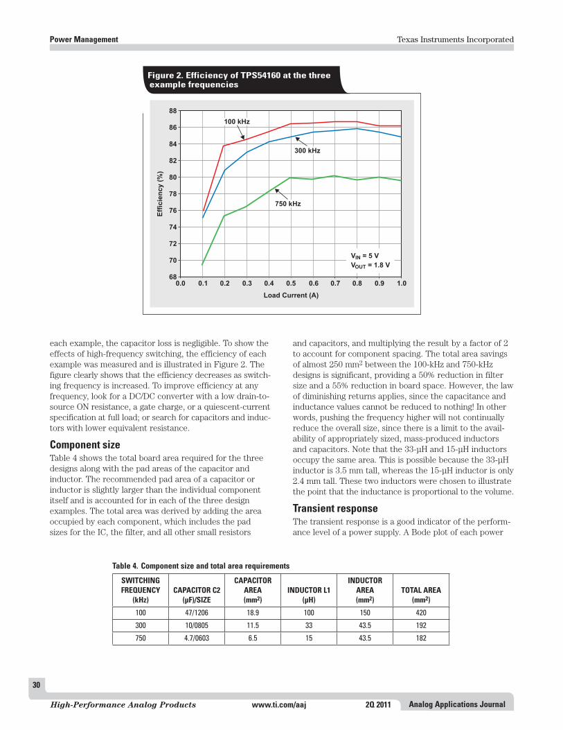
Texas Instruments Incorporated
30
Analog Applications JournalHigh-Performance Analog Products www.ti.com/aaj 2Q 2011
Power Management
each example, the capacitor loss is negligible. To show the effects of high-frequency switching, the efficiency of each example was measured and is illustrated in Figure 2. The figure clearly shows that the efficiency decreases as switch-ing frequency is increased. To improve efficiency at any frequency, look for a DC/DC converter with a low drain-to-source ON resistance, a gate charge, or a quiescent-current specification at full load; or search for capacitors and induc-tors with lower equivalent resistance.
Component sizeTable 4 shows the total board area required for the three designs along with the pad areas of the capacitor and inductor. The recommended pad area of a capacitor or inductor is slightly larger than the individual component itself and is accounted for in each of the three design examples. The total area was derived by adding the area occupied by each component, which includes the pad sizes for the IC, the filter, and all other small resistors
and capacitors, and multiplying the result by a factor of 2 to account for component spacing. The total area savings of almost 250 mm2 between the 100-kHz and 750-kHz designs is significant, providing a 50% reduction in filter size and a 55% reduction in board space. However, the law of diminishing returns applies, since the capacitance and inductance values cannot be reduced to nothing! In other words, pushing the frequency higher will not continually reduce the overall size, since there is a limit to the avail-ability of appropriately sized, mass-produced inductors and capacitors. Note that the 33-µH and 15-µH inductors occupy the same area. This is possible because the 33-µH inductor is 3.5 mm tall, whereas the 15-µH inductor is only 2.4 mm tall. These two inductors were chosen to illustrate the point that the inductance is proportional to the volume.
Transient responseThe transient response is a good indicator of the perform-ance level of a power supply. A Bode plot of each power
88
86
84
82
80
78
76
74
72
70
680.0 0.1 0.2 0.4 0.6 0.80.3 0.5 0.7 0.9 1.0
Load Current (A)
Eff
icie
nc
y (
%)
100 kHz
300 kHz
750 kHz
V = 5 V
V = 1.8 VIN
OUT
Figure 2. Efficiency of TPS54160 at the three example frequencies
Table 4. Component size and total area requirements
SWITCHING FREQUENCY
(kHz)CAPACITOR C2
(µF)/SIZE
CAPACITOR AREA(mm2)
INDUCTOR L1(µH)
INDUCTOR AREA(mm2)
TOTAL AREA(mm2)
100 47/1206 18 .9 100 150 420
300 10/0805 11 .5 33 43 .5 192
750 4 .7/0603 6 .5 15 43 .5 182

Texas Instruments Incorporated
31
Analog Applications Journal 2Q 2011 www.ti.com/aaj High-Performance Analog Products
Power Management
supply was taken to show a comparison at higher switching frequencies (see Figure 3). As shown, the phase margin of each power supply is between 45 and 55°, indicating a well- dampened transient response. The crossover frequency is approximately one-eighth of the switching frequency. When using a fast switching DC/DC converter, the designer should make sure the power IC’s error amplifier has enough bandwidth to support a high crossover frequency. The unity gain bandwidth of the TPS54160’s error amplifier is typically 2.7 MHz. The actual transient-response times are shown in Table 5 with the associated values for voltage-peak overshoot. The overshoot value is significantly lower with the higher switching frequency, due to the wider bandwidth.
Jitter considerationsNoise can be a problem with high conversion ratios and higher frequencies. When selecting a high switching fre-quency, the designer should consider jitter and the mini-mum ON time of the DC/DC converter. Jitter noise becomes a larger percentage of the switching pulse when the duty cycle is small. Table 6 shows the ratio of the jitter to the ON time for a 48-V-to-5-V conversion. A 0.5-V diode drop and a 20-ns jitter on the phase node are assumed.
ConclusionThere are trade-offs to designing high-frequency switching converters. Some of the advantages shown in this article are smaller size, faster transient response, and smaller voltage over-/undershoots. The main penalties paid for these are reduced efficiency and increased heat dissipation. There are also potential pitfalls in pushing the envelope,
such as pulse skipping and noise issues. Before a wide-input-voltage DC/DC converter for high-frequency applica-tions is selected, the manufacturer’s datasheet should be checked for important specifications such as the minimum ON time, the gain bandwidth of the error amplifier, the FET resistance, and the FET switching loss. ICs that per-form well with these specifications will cost a premium but will be worth the price and much easier to use when the designer is cornered with a tough design problem.
Related Web sitespower.ti.comwww.ti.com/sc/device/TPS54160
Table 5. Transient response
SWITCHING FREQUENCY
(kHz)
CROSSOVER FREQUENCY
(kHz)
PHASE MARGIN(degrees)
RESPONSE TIME(µs)
VOLTAGE PEAK(mV)
100 10 60 1000 350
300 30 60 300 300
750 60 50 150 240
Table 6. Ratio of jitter to ON time at small duty cycles
SWITCHING FREQUENCY
(kHz) ON TIMEJITTER/ON TIME
(%)
100 1 .1 µs 2
300 365 ns 5
750 150 ns 13
300 1 10 100 500
Frequency (kHz)
180
150
120
90
60
30
0
–30
–60
–90
–120
–150
–180
Gain
( dB
)
Ph
ase (
deg
rees)
60
50
40
30
20
10
0
–10
–20
–30
–40
–50
–60
750-kHzCrossover
100-kHzCrossover
300-kHzCrossover
Gain:100 kHz300 kHz750 kHz
Phase:100 kHz300 kHz750 kHz
Figure 3. Bode plots at 100, 300, and 750 kHz

32
Analog Applications Journal
Texas Instruments Incorporated
High-Performance Analog Products www.ti.com/aaj 2Q 2011
Index of Articles
Index of Articles Title Issue Page Lit. No.
Data AcquisitionAspects of data acquisition system design . . . . . . . . . . . . . . . . . . . . . . . . . . . . . . . . . . . . . . . . . . . . .August 1999 . . . . . . 1 SLYT191Low-power data acquisition sub-system using the TI TLV1572 . . . . . . . . . . . . . . . . . . . . . . . . . . . .August 1999 . . . . . . 4 SLYT192Evaluating operational amplifiers as input amplifiers for A-to-D converters . . . . . . . . . . . . . . . . .August 1999 . . . . . . 7 SLYT193Precision voltage references . . . . . . . . . . . . . . . . . . . . . . . . . . . . . . . . . . . . . . . . . . . . . . . . . . . . . . . .November 1999. . . . 1 SLYT183Techniques for sampling high-speed graphics with lower-speed A/D converters . . . . . . . . . . . . . .November 1999. . . . 5 SLYT184A methodology of interfacing serial A-to-D converters to DSPs . . . . . . . . . . . . . . . . . . . . . . . . . . .February 2000. . . . . 1 SLYT175The operation of the SAR-ADC based on charge redistribution. . . . . . . . . . . . . . . . . . . . . . . . . . . .February 2000. . . . 10 SLYT176The design and performance of a precision voltage reference circuit for 14-bit and
16-bit A-to-D and D-to-A converters . . . . . . . . . . . . . . . . . . . . . . . . . . . . . . . . . . . . . . . . . . . . . . .May 2000 . . . . . . . . . 1 SLYT168Introduction to phase-locked loop system modeling. . . . . . . . . . . . . . . . . . . . . . . . . . . . . . . . . . . . .May 2000 . . . . . . . . . 5 SLYT169New DSP development environment includes data converter plug-ins . . . . . . . . . . . . . . . . . . . . .August 2000 . . . . . . 1 SLYT158Higher data throughput for DSP analog-to-digital converters . . . . . . . . . . . . . . . . . . . . . . . . . . . . .August 2000 . . . . . . 5 SLYT159Efficiently interfacing serial data converters to high-speed DSPs . . . . . . . . . . . . . . . . . . . . . . . . .August 2000 . . . . . 10 SLYT160Smallest DSP-compatible ADC provides simplest DSP interface . . . . . . . . . . . . . . . . . . . . . . . . . . .November 2000. . . . 1 SLYT148Hardware auto-identification and software auto-configuration for the
TLV320AIC10 DSP Codec — a “plug-and-play” algorithm . . . . . . . . . . . . . . . . . . . . . . . . . . . . .November 2000. . . . 8 SLYT149Using quad and octal ADCs in SPI mode . . . . . . . . . . . . . . . . . . . . . . . . . . . . . . . . . . . . . . . . . . . . . .November 2000. . . 15 SLYT150Building a simple data acquisition system using the TMS320C31 DSP . . . . . . . . . . . . . . . . . . . . .February 2001. . . . . 1 SLYT136Using SPI synchronous communication with data converters — interfacing the
MSP430F149 and TLV5616 . . . . . . . . . . . . . . . . . . . . . . . . . . . . . . . . . . . . . . . . . . . . . . . . . . . . . .February 2001. . . . . 7 SLYT137A/D and D/A conversion of PC graphics and component video signals, Part 1: Hardware . . . . . .February 2001. . . . 11 SLYT138A/D and D/A conversion of PC graphics and component video signals, Part 2: Software
and control . . . . . . . . . . . . . . . . . . . . . . . . . . . . . . . . . . . . . . . . . . . . . . . . . . . . . . . . . . . . . . . . . . . .July 2001 . . . . . . . . . 5 SLYT129Intelligent sensor system maximizes battery life: Interfacing the MSP430F123
Flash MCU, ADS7822, and TPS60311 . . . . . . . . . . . . . . . . . . . . . . . . . . . . . . . . . . . . . . . . . . . . . .1Q, 2002 . . . . . . . . . 5 SLYT123SHDSL AFE1230 application . . . . . . . . . . . . . . . . . . . . . . . . . . . . . . . . . . . . . . . . . . . . . . . . . . . . . . . .2Q, 2002 . . . . . . . . . 5 SLYT114Synchronizing non-FIFO variations of the THS1206 . . . . . . . . . . . . . . . . . . . . . . . . . . . . . . . . . . . . .2Q, 2002 . . . . . . . . 12 SLYT115Adjusting the A/D voltage reference to provide gain. . . . . . . . . . . . . . . . . . . . . . . . . . . . . . . . . . . . .3Q, 2002 . . . . . . . . . 5 SLYT109MSC1210 debugging strategies for high-precision smart sensors . . . . . . . . . . . . . . . . . . . . . . . . . .3Q, 2002 . . . . . . . . . 7 SLYT110Using direct data transfer to maximize data acquisition throughput. . . . . . . . . . . . . . . . . . . . . . . .3Q, 2002 . . . . . . . . 14 SLYT111Interfacing op amps and analog-to-digital converters . . . . . . . . . . . . . . . . . . . . . . . . . . . . . . . . . . . .4Q, 2002 . . . . . . . . . 5 SLYT104ADS82x ADC with non-uniform sampling clock . . . . . . . . . . . . . . . . . . . . . . . . . . . . . . . . . . . . . . . .4Q, 2003 . . . . . . . . . 5 SLYT089Calculating noise figure and third-order intercept in ADCs . . . . . . . . . . . . . . . . . . . . . . . . . . . . . . .4Q, 2003 . . . . . . . . 11 SLYT090Evaluation criteria for ADSL analog front end. . . . . . . . . . . . . . . . . . . . . . . . . . . . . . . . . . . . . . . . . .4Q, 2003 . . . . . . . . 16 SLYT091Two-channel, 500-kSPS operation of the ADS8361 . . . . . . . . . . . . . . . . . . . . . . . . . . . . . . . . . . . . . .1Q, 2004 . . . . . . . . . 5 SLYT082ADS809 analog-to-digital converter with large input pulse signal . . . . . . . . . . . . . . . . . . . . . . . . . .1Q, 2004 . . . . . . . . . 8 SLYT083Streamlining the mixed-signal path with the signal-chain-on-chip MSP430F169. . . . . . . . . . . . . .3Q, 2004 . . . . . . . . . 5 SLYT078Supply voltage measurement and ADC PSRR improvement in MSC12xx devices . . . . . . . . . . . . .1Q, 2005 . . . . . . . . . 5 SLYT07314-bit, 125-MSPS ADS5500 evaluation . . . . . . . . . . . . . . . . . . . . . . . . . . . . . . . . . . . . . . . . . . . . . . . .1Q, 2005 . . . . . . . . 13 SLYT074Clocking high-speed data converters . . . . . . . . . . . . . . . . . . . . . . . . . . . . . . . . . . . . . . . . . . . . . . . . .1Q, 2005 . . . . . . . . 20 SLYT075Implementation of 12-bit delta-sigma DAC with MSC12xx controller . . . . . . . . . . . . . . . . . . . . . . .1Q, 2005 . . . . . . . . 27 SLYT076Using resistive touch screens for human/machine interface. . . . . . . . . . . . . . . . . . . . . . . . . . . . . . .3Q, 2005 . . . . . . . . . 5 SLYT209ASimple DSP interface for ADS784x/834x ADCs . . . . . . . . . . . . . . . . . . . . . . . . . . . . . . . . . . . . . . . . .3Q, 2005 . . . . . . . . 10 SLYT210Operating multiple oversampling data converters . . . . . . . . . . . . . . . . . . . . . . . . . . . . . . . . . . . . . . .4Q, 2005 . . . . . . . . . 5 SLYT222Low-power, high-intercept interface to the ADS5424 14-bit, 105-MSPS converter for
undersampling applications . . . . . . . . . . . . . . . . . . . . . . . . . . . . . . . . . . . . . . . . . . . . . . . . . . . . . .4Q, 2005 . . . . . . . . 10 SLYT223Understanding and comparing datasheets for high-speed ADCs . . . . . . . . . . . . . . . . . . . . . . . . . . .1Q, 2006 . . . . . . . . . 5 SLYT231Matching the noise performance of the operational amplifier to the ADC . . . . . . . . . . . . . . . . . . .2Q, 2006 . . . . . . . . . 5 SLYT237Using the ADS8361 with the MSP430 USI port . . . . . . . . . . . . . . . . . . . . . . . . . . . . . . . . . . . . . . . . .3Q, 2006 . . . . . . . . . 5 SLYT244Clamp function of high-speed ADC THS1041 . . . . . . . . . . . . . . . . . . . . . . . . . . . . . . . . . . . . . . . . . .4Q, 2006 . . . . . . . . . 5 SLYT253Conversion latency in delta-sigma converters . . . . . . . . . . . . . . . . . . . . . . . . . . . . . . . . . . . . . . . . . .2Q, 2007 . . . . . . . . . 5 SLYT264Calibration in touch-screen systems . . . . . . . . . . . . . . . . . . . . . . . . . . . . . . . . . . . . . . . . . . . . . . . . . .3Q, 2007 . . . . . . . . . 5 SLYT277Using a touch-screen controller’s auxiliary inputs . . . . . . . . . . . . . . . . . . . . . . . . . . . . . . . . . . . . . . .4Q, 2007 . . . . . . . . . 5 SLYT283

Texas Instruments Incorporated
33
Analog Applications Journal 2Q 2011 www.ti.com/aaj High-Performance Analog Products
Index of Articles
Title Issue Page Lit. No.
Data Acquisition (Continued)Understanding the pen-interrupt (PENIRQ) operation of touch-screen controllers . . . . . . . . . . .2Q, 2008 . . . . . . . . . 5 SLYT292A DAC for all precision occasions . . . . . . . . . . . . . . . . . . . . . . . . . . . . . . . . . . . . . . . . . . . . . . . . . . . .3Q, 2008 . . . . . . . . . 5 SLYT300Stop-band limitations of the Sallen-Key low-pass filter. . . . . . . . . . . . . . . . . . . . . . . . . . . . . . . . . . .4Q, 2008 . . . . . . . . . 5 SLYT306How the voltage reference affects ADC performance, Part 1. . . . . . . . . . . . . . . . . . . . . . . . . . . . . .2Q, 2009 . . . . . . . . . 5 SLYT331Impact of sampling-clock spurs on ADC performance . . . . . . . . . . . . . . . . . . . . . . . . . . . . . . . . . . .3Q, 2009 . . . . . . . . . 5 SLYT338How the voltage reference affects ADC performance, Part 2. . . . . . . . . . . . . . . . . . . . . . . . . . . . . .3Q, 2009 . . . . . . . . 13 SLYT339How the voltage reference affects ADC performance, Part 3. . . . . . . . . . . . . . . . . . . . . . . . . . . . . .4Q, 2009 . . . . . . . . . 5 SLYT355How digital filters affect analog audio-signal levels . . . . . . . . . . . . . . . . . . . . . . . . . . . . . . . . . . . . . .2Q, 2010 . . . . . . . . . 5 SLYT375Clock jitter analyzed in the time domain, Part 1 . . . . . . . . . . . . . . . . . . . . . . . . . . . . . . . . . . . . . . . .3Q, 2010 . . . . . . . . . 5 SLYT379Clock jitter analyzed in the time domain, Part 2 . . . . . . . . . . . . . . . . . . . . . . . . . . . . . . . . . . . . . . . .4Q, 2010 . . . . . . . . . 5 SLYT389The IBIS model: A conduit into signal-integrity analysis, Part 1 . . . . . . . . . . . . . . . . . . . . . . . . . . .4Q, 2010 . . . . . . . . 11 SLYT390The IBIS model, Part 2: Determining the total quality of an IBIS model. . . . . . . . . . . . . . . . . . . . .1Q, 2011 . . . . . . . . . 5 SLYT400The IBIS model, Part 3: Using IBIS models to investigate signal-integrity issues. . . . . . . . . . . . . .2Q, 2011 . . . . . . . . . 5 SLYT413
Power ManagementStability analysis of low-dropout linear regulators with a PMOS pass element. . . . . . . . . . . . . . . .August 1999 . . . . . 10 SLYT194Extended output voltage adjustment (0 V to 3.5 V) using the TI TPS5210 . . . . . . . . . . . . . . . . . .August 1999 . . . . . 13 SLYT195Migrating from the TI TL770x to the TI TLC770x. . . . . . . . . . . . . . . . . . . . . . . . . . . . . . . . . . . . . . .August 1999 . . . . . 14 SLYT196TI TPS5602 for powering TI’s DSP . . . . . . . . . . . . . . . . . . . . . . . . . . . . . . . . . . . . . . . . . . . . . . . . . . .November 1999. . . . 8 SLYT185Synchronous buck regulator design using the TI TPS5211 high-frequency
hysteretic controller . . . . . . . . . . . . . . . . . . . . . . . . . . . . . . . . . . . . . . . . . . . . . . . . . . . . . . . . . . . .November 1999. . . 10 SLYT186Understanding the stable range of equivalent series resistance of an LDO regulator . . . . . . . . . .November 1999. . . 14 SLYT187Power supply solutions for TI DSPs using synchronous buck converters . . . . . . . . . . . . . . . . . . . .February 2000. . . . 12 SLYT177Powering Celeron-type microprocessors using TI’s TPS5210 and TPS5211 controllers . . . . . . . .February 2000. . . . 20 SLYT178Simple design of an ultra-low-ripple DC/DC boost converter with TPS60100 charge pump. . . . .May 2000 . . . . . . . . 11 SLYT170Low-cost, minimum-size solution for powering future-generation Celeron™-type
processors with peak currents up to 26 A. . . . . . . . . . . . . . . . . . . . . . . . . . . . . . . . . . . . . . . . . . .May 2000 . . . . . . . . 14 SLYT171Advantages of using PMOS-type low-dropout linear regulators in battery applications . . . . . . . .August 2000 . . . . . 16 SLYT161Optimal output filter design for microprocessor or DSP power supply . . . . . . . . . . . . . . . . . . . . .August 2000 . . . . . 22 SLYT162Understanding the load-transient response of LDOs . . . . . . . . . . . . . . . . . . . . . . . . . . . . . . . . . . . .November 2000. . . 19 SLYT151Comparison of different power supplies for portable DSP solutions
working from a single-cell battery . . . . . . . . . . . . . . . . . . . . . . . . . . . . . . . . . . . . . . . . . . . . . . . . .November 2000. . . 24 SLYT152Optimal design for an interleaved synchronous buck converter under high-slew-rate,
load-current transient conditions . . . . . . . . . . . . . . . . . . . . . . . . . . . . . . . . . . . . . . . . . . . . . . . . .February 2001. . . . 15 SLYT139–48-V/+48-V hot-swap applications . . . . . . . . . . . . . . . . . . . . . . . . . . . . . . . . . . . . . . . . . . . . . . . . . .February 2001. . . . 20 SLYT140Power supply solution for DDR bus termination . . . . . . . . . . . . . . . . . . . . . . . . . . . . . . . . . . . . . . . .July 2001 . . . . . . . . . 9 SLYT130Runtime power control for DSPs using the TPS62000 buck converter . . . . . . . . . . . . . . . . . . . . . .July 2001 . . . . . . . . 15 SLYT131Power control design key to realizing InfiniBandSM benefits. . . . . . . . . . . . . . . . . . . . . . . . . . . . . . .1Q, 2002 . . . . . . . . 10 SLYT124Comparing magnetic and piezoelectric transformer approaches in CCFL applications . . . . . . . . .1Q, 2002 . . . . . . . . 12 SLYT125Why use a wall adapter for ac input power? . . . . . . . . . . . . . . . . . . . . . . . . . . . . . . . . . . . . . . . . . . .1Q, 2002 . . . . . . . . 18 SLYT126SWIFT™ Designer power supply design program. . . . . . . . . . . . . . . . . . . . . . . . . . . . . . . . . . . . . . .2Q, 2002 . . . . . . . . 15 SLYT116Optimizing the switching frequency of ADSL power supplies . . . . . . . . . . . . . . . . . . . . . . . . . . . . .2Q, 2002 . . . . . . . . 23 SLYT117Powering electronics from the USB port . . . . . . . . . . . . . . . . . . . . . . . . . . . . . . . . . . . . . . . . . . . . . .2Q, 2002 . . . . . . . . 28 SLYT118Using the UCC3580-1 controller for highly efficient 3.3-V/100-W isolated supply design . . . . . . .4Q, 2002 . . . . . . . . . 8 SLYT105Power conservation options with dynamic voltage scaling in portable DSP designs . . . . . . . . . . .4Q, 2002 . . . . . . . . 12 SLYT106Understanding piezoelectric transformers in CCFL backlight applications. . . . . . . . . . . . . . . . . . .4Q, 2002 . . . . . . . . 18 SLYT107Load-sharing techniques: Paralleling power modules with overcurrent protection . . . . . . . . . . . .1Q, 2003 . . . . . . . . . 5 SLYT100Using the TPS61042 white-light LED driver as a boost converter . . . . . . . . . . . . . . . . . . . . . . . . . .1Q, 2003 . . . . . . . . . 7 SLYT101Auto-Track™ voltage sequencing simplifies simultaneous power-up and power-down. . . . . . . . .3Q, 2003 . . . . . . . . . 5 SLYT095Soft-start circuits for LDO linear regulators. . . . . . . . . . . . . . . . . . . . . . . . . . . . . . . . . . . . . . . . . . . .3Q, 2003 . . . . . . . . 10 SLYT096UCC28517 100-W PFC power converter with 12-V, 8-W bias supply, Part 1. . . . . . . . . . . . . . . . . .3Q, 2003 . . . . . . . . 13 SLYT097UCC28517 100-W PFC power converter with 12-V, 8-W bias supply, Part 2. . . . . . . . . . . . . . . . . .4Q, 2003 . . . . . . . . 21 SLYT092LED-driver considerations . . . . . . . . . . . . . . . . . . . . . . . . . . . . . . . . . . . . . . . . . . . . . . . . . . . . . . . . . .1Q, 2004 . . . . . . . . 14 SLYT084Tips for successful power-up of today’s high-performance FPGAs . . . . . . . . . . . . . . . . . . . . . . . . .3Q, 2004 . . . . . . . . 11 SLYT079A better bootstrap/bias supply circuit. . . . . . . . . . . . . . . . . . . . . . . . . . . . . . . . . . . . . . . . . . . . . . . . .1Q, 2005 . . . . . . . . 33 SLYT077Understanding noise in linear regulators . . . . . . . . . . . . . . . . . . . . . . . . . . . . . . . . . . . . . . . . . . . . . .2Q, 2005 . . . . . . . . . 5 SLYT201Understanding power supply ripple rejection in linear regulators . . . . . . . . . . . . . . . . . . . . . . . . . .2Q, 2005 . . . . . . . . . 8 SLYT202

Texas Instruments Incorporated
34
Analog Applications JournalHigh-Performance Analog Products www.ti.com/aaj 2Q 2011
Index of Articles
Title Issue Page Lit. No.
Power Management (Continued)Miniature solutions for voltage isolation . . . . . . . . . . . . . . . . . . . . . . . . . . . . . . . . . . . . . . . . . . . . . . .3Q, 2005 . . . . . . . . 13 SLYT211New power modules improve surface-mount manufacturability . . . . . . . . . . . . . . . . . . . . . . . . . . .3Q, 2005 . . . . . . . . 18 SLYT212Li-ion switching charger integrates power FETs . . . . . . . . . . . . . . . . . . . . . . . . . . . . . . . . . . . . . . . .4Q, 2005 . . . . . . . . 19 SLYT224TLC5940 dot correction compensates for variations in LED brightness . . . . . . . . . . . . . . . . . . . . .4Q, 2005 . . . . . . . . 21 SLYT225Powering today’s multi-rail FPGAs and DSPs, Part 1 . . . . . . . . . . . . . . . . . . . . . . . . . . . . . . . . . . . .1Q, 2006 . . . . . . . . . 9 SLYT232TPS79918 RF LDO supports migration to StrataFlash® Embedded Memory (P30) . . . . . . . . . . .1Q, 2006 . . . . . . . . 14 SLYT233Practical considerations when designing a power supply with the TPS6211x . . . . . . . . . . . . . . . .1Q, 2006 . . . . . . . . 17 SLYT234TLC5940 PWM dimming provides superior color quality in LED video displays . . . . . . . . . . . . . .2Q, 2006 . . . . . . . . 10 SLYT238Wide-input dc/dc modules offer maximum design flexibility . . . . . . . . . . . . . . . . . . . . . . . . . . . . . .2Q, 2006 . . . . . . . . 13 SLYT239Powering today’s multi-rail FPGAs and DSPs, Part 2 . . . . . . . . . . . . . . . . . . . . . . . . . . . . . . . . . . . .2Q, 2006 . . . . . . . . 18 SLYT240TPS61059 powers white-light LED as photoflash or movie light . . . . . . . . . . . . . . . . . . . . . . . . . . .3Q, 2006 . . . . . . . . . 8 SLYT245TPS65552A powers portable photoflash. . . . . . . . . . . . . . . . . . . . . . . . . . . . . . . . . . . . . . . . . . . . . . .3Q, 2006 . . . . . . . . 10 SLYT246Single-chip bq2403x power-path manager charges battery while powering system . . . . . . . . . . . .3Q, 2006 . . . . . . . . 12 SLYT247Complete battery-pack design for one- or two-cell portable applications . . . . . . . . . . . . . . . . . . . .3Q, 2006 . . . . . . . . 14 SLYT248A 3-A, 1.2-VOUT linear regulator with 80% efficiency and PLOST < 1 W . . . . . . . . . . . . . . . . . . . . . .4Q, 2006 . . . . . . . . 10 SLYT254bq25012 single-chip, Li-ion charger and dc/dc converter for Bluetooth® headsets . . . . . . . . . . . .4Q, 2006 . . . . . . . . 13 SLYT255Fully integrated TPS6300x buck-boost converter extends Li-ion battery life. . . . . . . . . . . . . . . . .4Q, 2006 . . . . . . . . 15 SLYT256Selecting the correct IC for power-supply applications. . . . . . . . . . . . . . . . . . . . . . . . . . . . . . . . . . .1Q, 2007 . . . . . . . . . 5 SLYT259LDO white-LED driver TPS7510x provides incredibly small solution size . . . . . . . . . . . . . . . . . . .1Q, 2007 . . . . . . . . . 9 SLYT260Power management for processor core voltage requirements . . . . . . . . . . . . . . . . . . . . . . . . . . . . .1Q, 2007 . . . . . . . . 11 SLYT261Enhanced-safety, linear Li-ion battery charger with thermal regulation and
input overvoltage protection . . . . . . . . . . . . . . . . . . . . . . . . . . . . . . . . . . . . . . . . . . . . . . . . . . . . .2Q, 2007 . . . . . . . . . 8 SLYT269Current balancing in four-pair, high-power PoE applications. . . . . . . . . . . . . . . . . . . . . . . . . . . . . .2Q, 2007 . . . . . . . . 11 SLYT270Power-management solutions for telecom systems improve performance, cost, and size. . . . . . .3Q, 2007 . . . . . . . . 10 SLYT278TPS6108x: A boost converter with extreme versatility. . . . . . . . . . . . . . . . . . . . . . . . . . . . . . . . . . .3Q, 2007 . . . . . . . . 14 SLYT279Get low-noise, low-ripple, high-PSRR power with the TPS717xx . . . . . . . . . . . . . . . . . . . . . . . . . .3Q, 2007 . . . . . . . . 17 SLYT280Simultaneous power-down sequencing with the TPS74x01 family of linear regulators . . . . . . . . .3Q, 2007 . . . . . . . . 20 SLYT281Driving a WLED does not always require 4 V . . . . . . . . . . . . . . . . . . . . . . . . . . . . . . . . . . . . . . . . . .4Q, 2007 . . . . . . . . . 9 SLYT284Host-side gas-gauge-system design considerations for single-cell handheld applications . . . . . . .4Q, 2007 . . . . . . . . 12 SLYT285Using a buck converter in an inverting buck-boost topology . . . . . . . . . . . . . . . . . . . . . . . . . . . . . .4Q, 2007 . . . . . . . . 16 SLYT286Understanding output voltage limitations of DC/DC buck converters . . . . . . . . . . . . . . . . . . . . . . .2Q, 2008 . . . . . . . . 11 SLYT293Battery-charger front-end IC improves charging-system safety. . . . . . . . . . . . . . . . . . . . . . . . . . . .2Q, 2008 . . . . . . . . 14 SLYT294New current-mode PWM controllers support boost, flyback, SEPIC, and
LED-driver applications . . . . . . . . . . . . . . . . . . . . . . . . . . . . . . . . . . . . . . . . . . . . . . . . . . . . . . . . .3Q, 2008 . . . . . . . . . 9 SLYT302Getting the most battery life from portable systems. . . . . . . . . . . . . . . . . . . . . . . . . . . . . . . . . . . . .4Q, 2008 . . . . . . . . . 8 SLYT307Compensating and measuring the control loop of a high-power LED driver . . . . . . . . . . . . . . . . .4Q, 2008 . . . . . . . . 14 SLYT308Designing DC/DC converters based on SEPIC topology . . . . . . . . . . . . . . . . . . . . . . . . . . . . . . . . . .4Q, 2008 . . . . . . . . 18 SLYT309Paralleling power modules for high-current applications . . . . . . . . . . . . . . . . . . . . . . . . . . . . . . . . .1Q, 2009 . . . . . . . . . 5 SLYT320Improving battery safety, charging, and fuel gauging in portable media applications . . . . . . . . . .1Q, 2009 . . . . . . . . . 9 SLYT321Cell balancing buys extra run time and battery life. . . . . . . . . . . . . . . . . . . . . . . . . . . . . . . . . . . . . .1Q, 2009 . . . . . . . . 14 SLYT322Using a portable-power boost converter in an isolated flyback application . . . . . . . . . . . . . . . . . .1Q, 2009 . . . . . . . . 19 SLYT323Taming linear-regulator inrush currents . . . . . . . . . . . . . . . . . . . . . . . . . . . . . . . . . . . . . . . . . . . . . . .2Q, 2009 . . . . . . . . . 9 SLYT332Designing a linear Li-Ion battery charger with power-path control . . . . . . . . . . . . . . . . . . . . . . . . .2Q, 2009 . . . . . . . . 12 SLYT333Selecting the right charge-management solution. . . . . . . . . . . . . . . . . . . . . . . . . . . . . . . . . . . . . . . .2Q, 2009 . . . . . . . . 18 SLYT334Reducing radiated EMI in WLED drivers . . . . . . . . . . . . . . . . . . . . . . . . . . . . . . . . . . . . . . . . . . . . . .3Q, 2009 . . . . . . . . 17 SLYT340Using power solutions to extend battery life in MSP430 applications . . . . . . . . . . . . . . . . . . . . . . .4Q, 2009 . . . . . . . . 10 SLYT356Designing a multichemistry battery charger . . . . . . . . . . . . . . . . . . . . . . . . . . . . . . . . . . . . . . . . . . .4Q, 2009 . . . . . . . . 13 SLYT357Efficiency of synchronous versus nonsynchronous buck converters. . . . . . . . . . . . . . . . . . . . . . . .4Q, 2009 . . . . . . . . 15 SLYT358Fuel-gauging considerations in battery backup storage systems . . . . . . . . . . . . . . . . . . . . . . . . . . .1Q, 2010 . . . . . . . . . 5 SLYT364Li-ion battery-charger solutions for JEITA compliance. . . . . . . . . . . . . . . . . . . . . . . . . . . . . . . . . . .1Q, 2010 . . . . . . . . . 8 SLYT365Power-supply design for high-speed ADCs. . . . . . . . . . . . . . . . . . . . . . . . . . . . . . . . . . . . . . . . . . . . .1Q, 2010 . . . . . . . . 12 SLYT366Discrete design of a low-cost isolated 3.3- to 5-V DC/DC converter . . . . . . . . . . . . . . . . . . . . . . . .2Q, 2010 . . . . . . . . 12 SLYT371Designing DC/DC converters based on ZETA topology. . . . . . . . . . . . . . . . . . . . . . . . . . . . . . . . . . .2Q, 2010 . . . . . . . . 16 SLYT372Coupled inductors broaden DC/DC converter usage. . . . . . . . . . . . . . . . . . . . . . . . . . . . . . . . . . . . .3Q, 2010 . . . . . . . . 10 SLYT380Computing power going “Platinum” . . . . . . . . . . . . . . . . . . . . . . . . . . . . . . . . . . . . . . . . . . . . . . . . . .3Q, 2010 . . . . . . . . 13 SLYT382A low-cost, non-isolated AC/DC buck converter with no transformer. . . . . . . . . . . . . . . . . . . . . . .4Q, 2010 . . . . . . . . 16 SLYT391Save power with a soft Zener clamp . . . . . . . . . . . . . . . . . . . . . . . . . . . . . . . . . . . . . . . . . . . . . . . . . .4Q, 2010 . . . . . . . . 19 SLYT392

Texas Instruments Incorporated
35
Analog Applications Journal 2Q 2011 www.ti.com/aaj High-Performance Analog Products
Index of Articles
Title Issue Page Lit. No.
Power Management (Continued)An introduction to the Wireless Power Consortium standard and TI’s compliant solutions . . . . .1Q, 2011 . . . . . . . . 10 SLYT401Fine-tuning TI’s Impedance Track™ battery fuel gauge with LiFePO4 cells in
shallow-discharge applications . . . . . . . . . . . . . . . . . . . . . . . . . . . . . . . . . . . . . . . . . . . . . . . . . . . .1Q, 2011 . . . . . . . . 13 SLYT402Implementation of microprocessor-controlled, wide-input-voltage, SMBus smart
battery charger . . . . . . . . . . . . . . . . . . . . . . . . . . . . . . . . . . . . . . . . . . . . . . . . . . . . . . . . . . . . . . . .2Q, 2011 . . . . . . . . 11 SLYT410Benefits of a coupled-inductor SEPIC converter . . . . . . . . . . . . . . . . . . . . . . . . . . . . . . . . . . . . . . . .2Q, 2011 . . . . . . . . 14 SLYT411IQ: What it is, what it isn’t, and how to use it . . . . . . . . . . . . . . . . . . . . . . . . . . . . . . . . . . . . . . . . . . .2Q, 2011 . . . . . . . . 18 SLYT412Backlighting the tablet PC . . . . . . . . . . . . . . . . . . . . . . . . . . . . . . . . . . . . . . . . . . . . . . . . . . . . . . . . . .2Q, 2011 . . . . . . . . 23 SLYT414Challenges of designing high-frequency, high-input-voltage DC/DC converters. . . . . . . . . . . . . . .2Q, 2011 . . . . . . . . 28 SLYT415
Interface (Data Transmission)TIA/EIA-568A Category 5 cables in low-voltage differential signaling (LVDS). . . . . . . . . . . . . . . .August 1999 . . . . . 16 SLYT197Keep an eye on the LVDS input levels . . . . . . . . . . . . . . . . . . . . . . . . . . . . . . . . . . . . . . . . . . . . . . . .November 1999. . . 17 SLYT188Skew definition and jitter analysis. . . . . . . . . . . . . . . . . . . . . . . . . . . . . . . . . . . . . . . . . . . . . . . . . . . .February 2000. . . . 29 SLYT179LVDS receivers solve problems in non-LVDS applications . . . . . . . . . . . . . . . . . . . . . . . . . . . . . . . .February 2000. . . . 33 SLYT180LVDS: The ribbon cable connection . . . . . . . . . . . . . . . . . . . . . . . . . . . . . . . . . . . . . . . . . . . . . . . . . .May 2000 . . . . . . . . 19 SLYT172Performance of LVDS with different cables . . . . . . . . . . . . . . . . . . . . . . . . . . . . . . . . . . . . . . . . . . .August 2000 . . . . . 30 SLYT163A statistical survey of common-mode noise . . . . . . . . . . . . . . . . . . . . . . . . . . . . . . . . . . . . . . . . . . .November 2000. . . 30 SLYT153The Active Fail-Safe feature of the SN65LVDS32A . . . . . . . . . . . . . . . . . . . . . . . . . . . . . . . . . . . . .November 2000. . . 35 SLYT154The SN65LVDS33/34 as an ECL-to-LVTTL converter . . . . . . . . . . . . . . . . . . . . . . . . . . . . . . . . . . . .July 2001 . . . . . . . . 19 SLYT132Power consumption of LVPECL and LVDS. . . . . . . . . . . . . . . . . . . . . . . . . . . . . . . . . . . . . . . . . . . . .1Q, 2002 . . . . . . . . 23 SLYT127Estimating available application power for Power-over-Ethernet applications . . . . . . . . . . . . . . . .1Q, 2004 . . . . . . . . 18 SLYT085The RS-485 unit load and maximum number of bus connections . . . . . . . . . . . . . . . . . . . . . . . . . .1Q, 2004 . . . . . . . . 21 SLYT086Failsafe in RS-485 data buses . . . . . . . . . . . . . . . . . . . . . . . . . . . . . . . . . . . . . . . . . . . . . . . . . . . . . . .3Q, 2004 . . . . . . . . 16 SLYT080Maximizing signal integrity with M-LVDS backplanes . . . . . . . . . . . . . . . . . . . . . . . . . . . . . . . . . . . .2Q, 2005 . . . . . . . . 11 SLYT203Device spacing on RS-485 buses . . . . . . . . . . . . . . . . . . . . . . . . . . . . . . . . . . . . . . . . . . . . . . . . . . . . .2Q, 2006 . . . . . . . . 25 SLYT241Improved CAN network security with TI’s SN65HVD1050 transceiver . . . . . . . . . . . . . . . . . . . . . .3Q, 2006 . . . . . . . . 17 SLYT249Detection of RS-485 signal loss . . . . . . . . . . . . . . . . . . . . . . . . . . . . . . . . . . . . . . . . . . . . . . . . . . . . . .4Q, 2006 . . . . . . . . 18 SLYT257Enabling high-speed USB OTG functionality on TI DSPs . . . . . . . . . . . . . . . . . . . . . . . . . . . . . . . . .2Q, 2007 . . . . . . . . 18 SLYT271When good grounds turn bad—isolate!. . . . . . . . . . . . . . . . . . . . . . . . . . . . . . . . . . . . . . . . . . . . . . . .3Q, 2008 . . . . . . . . 11 SLYT298Cascading of input serializers boosts channel density for digital inputs . . . . . . . . . . . . . . . . . . . . .3Q, 2008 . . . . . . . . 16 SLYT301RS-485: Passive failsafe for an idle bus. . . . . . . . . . . . . . . . . . . . . . . . . . . . . . . . . . . . . . . . . . . . . . . .1Q, 2009 . . . . . . . . 22 SLYT324Message priority inversion on a CAN bus . . . . . . . . . . . . . . . . . . . . . . . . . . . . . . . . . . . . . . . . . . . . . .1Q, 2009 . . . . . . . . 25 SLYT325Designing with digital isolators . . . . . . . . . . . . . . . . . . . . . . . . . . . . . . . . . . . . . . . . . . . . . . . . . . . . . .2Q, 2009 . . . . . . . . 21 SLYT335Magnetic-field immunity of digital capacitive isolators . . . . . . . . . . . . . . . . . . . . . . . . . . . . . . . . . . .3Q, 2010 . . . . . . . . 19 SLYT381Interfacing high-voltage applications to low-power controllers . . . . . . . . . . . . . . . . . . . . . . . . . . . .4Q, 2010 . . . . . . . . 20 SLYT393Designing an isolated I2C Bus® interface by using digital isolators . . . . . . . . . . . . . . . . . . . . . . . . .1Q, 2011 . . . . . . . . 17 SLYT403
Amplifiers: AudioReducing the output filter of a Class-D amplifier . . . . . . . . . . . . . . . . . . . . . . . . . . . . . . . . . . . . . . .August 1999 . . . . . 19 SLYT198Power supply decoupling and audio signal filtering for the Class-D audio power amplifier . . . . .August 1999 . . . . . 24 SLYT199PCB layout for the TPA005D1x and TPA032D0x Class-D APAs. . . . . . . . . . . . . . . . . . . . . . . . . . . .February 2000. . . . 39 SLYT182An audio circuit collection, Part 1 . . . . . . . . . . . . . . . . . . . . . . . . . . . . . . . . . . . . . . . . . . . . . . . . . . .November 2000. . . 39 SLYT1551.6- to 3.6-volt BTL speaker driver reference design . . . . . . . . . . . . . . . . . . . . . . . . . . . . . . . . . . . .February 2001. . . . 23 SLYT141Notebook computer upgrade path for audio power amplifiers . . . . . . . . . . . . . . . . . . . . . . . . . . . .February 2001. . . . 27 SLYT142An audio circuit collection, Part 2 . . . . . . . . . . . . . . . . . . . . . . . . . . . . . . . . . . . . . . . . . . . . . . . . . . .February 2001. . . . 41 SLYT145An audio circuit collection, Part 3. . . . . . . . . . . . . . . . . . . . . . . . . . . . . . . . . . . . . . . . . . . . . . . . . . . .July 2001 . . . . . . . . 34 SLYT134Audio power amplifier measurements . . . . . . . . . . . . . . . . . . . . . . . . . . . . . . . . . . . . . . . . . . . . . . . .July 2001 . . . . . . . . 40 SLYT135Audio power amplifier measurements, Part 2 . . . . . . . . . . . . . . . . . . . . . . . . . . . . . . . . . . . . . . . . . .1Q, 2002 . . . . . . . . 26 SLYT128Precautions for connecting APA outputs to other devices . . . . . . . . . . . . . . . . . . . . . . . . . . . . . . . .2Q, 2010 . . . . . . . . 22 SLYT373

Texas Instruments Incorporated
36
Analog Applications JournalHigh-Performance Analog Products www.ti.com/aaj 2Q 2011
Index of Articles
Title Issue Page Lit. No.
Amplifiers: Op AmpsSingle-supply op amp design . . . . . . . . . . . . . . . . . . . . . . . . . . . . . . . . . . . . . . . . . . . . . . . . . . . . . . . .November 1999. . . 20 SLYT189Reducing crosstalk of an op amp on a PCB . . . . . . . . . . . . . . . . . . . . . . . . . . . . . . . . . . . . . . . . . . . .November 1999. . . 23 SLYT190Matching operational amplifier bandwidth with applications . . . . . . . . . . . . . . . . . . . . . . . . . . . . . .February 2000. . . . 36 SLYT181Sensor to ADC — analog interface design . . . . . . . . . . . . . . . . . . . . . . . . . . . . . . . . . . . . . . . . . . . . .May 2000 . . . . . . . . 22 SLYT173Using a decompensated op amp for improved performance . . . . . . . . . . . . . . . . . . . . . . . . . . . . . .May 2000 . . . . . . . . 26 SLYT174Design of op amp sine wave oscillators . . . . . . . . . . . . . . . . . . . . . . . . . . . . . . . . . . . . . . . . . . . . . . .August 2000 . . . . . 33 SLYT164Fully differential amplifiers . . . . . . . . . . . . . . . . . . . . . . . . . . . . . . . . . . . . . . . . . . . . . . . . . . . . . . . . .August 2000 . . . . . 38 SLYT165The PCB is a component of op amp design . . . . . . . . . . . . . . . . . . . . . . . . . . . . . . . . . . . . . . . . . . . .August 2000 . . . . . 42 SLYT166Reducing PCB design costs: From schematic capture to PCB layout . . . . . . . . . . . . . . . . . . . . . . .August 2000 . . . . . 48 SLYT167Thermistor temperature transducer-to-ADC application . . . . . . . . . . . . . . . . . . . . . . . . . . . . . . . . .November 2000. . . 44 SLYT156Analysis of fully differential amplifiers . . . . . . . . . . . . . . . . . . . . . . . . . . . . . . . . . . . . . . . . . . . . . . . .November 2000. . . 48 SLYT157Fully differential amplifiers applications: Line termination, driving high-speed ADCs,
and differential transmission lines . . . . . . . . . . . . . . . . . . . . . . . . . . . . . . . . . . . . . . . . . . . . . . . .February 2001. . . . 32 SLYT143Pressure transducer-to-ADC application . . . . . . . . . . . . . . . . . . . . . . . . . . . . . . . . . . . . . . . . . . . . . .February 2001. . . . 38 SLYT144Frequency response errors in voltage feedback op amps . . . . . . . . . . . . . . . . . . . . . . . . . . . . . . . .February 2001. . . . 48 SLYT146Designing for low distortion with high-speed op amps . . . . . . . . . . . . . . . . . . . . . . . . . . . . . . . . . . .July 2001 . . . . . . . . 25 SLYT133Fully differential amplifier design in high-speed data acquisition systems . . . . . . . . . . . . . . . . . . .2Q, 2002 . . . . . . . . 35 SLYT119Worst-case design of op amp circuits . . . . . . . . . . . . . . . . . . . . . . . . . . . . . . . . . . . . . . . . . . . . . . . . .2Q, 2002 . . . . . . . . 42 SLYT120Using high-speed op amps for high-performance RF design, Part 1 . . . . . . . . . . . . . . . . . . . . . . . .2Q, 2002 . . . . . . . . 46 SLYT121Using high-speed op amps for high-performance RF design, Part 2 . . . . . . . . . . . . . . . . . . . . . . . .3Q, 2002 . . . . . . . . 21 SLYT112FilterPro™ low-pass design tool . . . . . . . . . . . . . . . . . . . . . . . . . . . . . . . . . . . . . . . . . . . . . . . . . . . . .3Q, 2002 . . . . . . . . 24 SLYT113Active output impedance for ADSL line drivers . . . . . . . . . . . . . . . . . . . . . . . . . . . . . . . . . . . . . . . .4Q, 2002 . . . . . . . . 24 SLYT108RF and IF amplifiers with op amps . . . . . . . . . . . . . . . . . . . . . . . . . . . . . . . . . . . . . . . . . . . . . . . . . . .1Q, 2003 . . . . . . . . . 9 SLYT102Analyzing feedback loops containing secondary amplifiers . . . . . . . . . . . . . . . . . . . . . . . . . . . . . . .1Q, 2003 . . . . . . . . 14 SLYT103Video switcher using high-speed op amps . . . . . . . . . . . . . . . . . . . . . . . . . . . . . . . . . . . . . . . . . . . . .3Q, 2003 . . . . . . . . 20 SLYT098Expanding the usability of current-feedback amplifiers . . . . . . . . . . . . . . . . . . . . . . . . . . . . . . . . . .3Q, 2003 . . . . . . . . 23 SLYT099Calculating noise figure in op amps . . . . . . . . . . . . . . . . . . . . . . . . . . . . . . . . . . . . . . . . . . . . . . . . . .4Q, 2003 . . . . . . . . 31 SLYT094Op amp stability and input capacitance . . . . . . . . . . . . . . . . . . . . . . . . . . . . . . . . . . . . . . . . . . . . . . .1Q, 2004 . . . . . . . . 24 SLYT087Integrated logarithmic amplifiers for industrial applications . . . . . . . . . . . . . . . . . . . . . . . . . . . . . .1Q, 2004 . . . . . . . . 28 SLYT088Active filters using current-feedback amplifiers . . . . . . . . . . . . . . . . . . . . . . . . . . . . . . . . . . . . . . . .3Q, 2004 . . . . . . . . 21 SLYT081Auto-zero amplifiers ease the design of high-precision circuits . . . . . . . . . . . . . . . . . . . . . . . . . . . .2Q, 2005 . . . . . . . . 19 SLYT204So many amplifiers to choose from: Matching amplifiers to applications . . . . . . . . . . . . . . . . . . . .3Q, 2005 . . . . . . . . 24 SLYT213Getting the most out of your instrumentation amplifier design . . . . . . . . . . . . . . . . . . . . . . . . . . . .4Q, 2005 . . . . . . . . 25 SLYT226High-speed notch filters . . . . . . . . . . . . . . . . . . . . . . . . . . . . . . . . . . . . . . . . . . . . . . . . . . . . . . . . . . . .1Q, 2006 . . . . . . . . 19 SLYT235Low-cost current-shunt monitor IC revives moving-coil meter design . . . . . . . . . . . . . . . . . . . . . .2Q, 2006 . . . . . . . . 27 SLYT242Accurately measuring ADC driving-circuit settling time. . . . . . . . . . . . . . . . . . . . . . . . . . . . . . . . . .1Q, 2007 . . . . . . . . 14 SLYT262New zero-drift amplifier has an IQ of 17 µA . . . . . . . . . . . . . . . . . . . . . . . . . . . . . . . . . . . . . . . . . . . .2Q, 2007 . . . . . . . . 22 SLYT272A new filter topology for analog high-pass filters . . . . . . . . . . . . . . . . . . . . . . . . . . . . . . . . . . . . . . .3Q, 2008 . . . . . . . . 18 SLYT299Input impedance matching with fully differential amplifiers . . . . . . . . . . . . . . . . . . . . . . . . . . . . . .4Q, 2008 . . . . . . . . 24 SLYT310A dual-polarity, bidirectional current-shunt monitor. . . . . . . . . . . . . . . . . . . . . . . . . . . . . . . . . . . . .4Q, 2008 . . . . . . . . 29 SLYT311Output impedance matching with fully differential operational amplifiers . . . . . . . . . . . . . . . . . . .1Q, 2009 . . . . . . . . 29 SLYT326Using fully differential op amps as attenuators, Part 1: Differential bipolar input signals . . . . . . .2Q, 2009 . . . . . . . . 33 SLYT336Using fully differential op amps as attenuators, Part 2: Single-ended bipolar input signals . . . . .3Q, 2009 . . . . . . . . 21 SLYT341Interfacing op amps to high-speed DACs, Part 1: Current-sinking DACs . . . . . . . . . . . . . . . . . . . .3Q, 2009 . . . . . . . . 24 SLYT342Using the infinite-gain, MFB filter topology in fully differential active filters . . . . . . . . . . . . . . . . .3Q, 2009 . . . . . . . . 33 SLYT343Using fully differential op amps as attenuators, Part 3: Single-ended unipolar input signals . . . .4Q, 2009 . . . . . . . . 19 SLYT359Interfacing op amps to high-speed DACs, Part 2: Current-sourcing DACs . . . . . . . . . . . . . . . . . . .4Q, 2009 . . . . . . . . 23 SLYT360Operational amplifier gain stability, Part 1: General system analysis. . . . . . . . . . . . . . . . . . . . . . . .1Q, 2010 . . . . . . . . 20 SLYT367Signal conditioning for piezoelectric sensors . . . . . . . . . . . . . . . . . . . . . . . . . . . . . . . . . . . . . . . . . . .1Q, 2010 . . . . . . . . 24 SLYT369Interfacing op amps to high-speed DACs, Part 3: Current-sourcing DACs simplified . . . . . . . . . .1Q, 2010 . . . . . . . . 32 SLYT368Operational amplifier gain stability, Part 2: DC gain-error analysis . . . . . . . . . . . . . . . . . . . . . . . . .2Q, 2010 . . . . . . . . 24 SLYT374Operational amplifier gain stability, Part 3: AC gain-error analysis . . . . . . . . . . . . . . . . . . . . . . . . .3Q, 2010 . . . . . . . . 23 SLYT383Using single-supply fully differential amplifiers with negative input voltages
to drive ADCs. . . . . . . . . . . . . . . . . . . . . . . . . . . . . . . . . . . . . . . . . . . . . . . . . . . . . . . . . . . . . . . . . .4Q, 2010 . . . . . . . . 26 SLYT394

Texas Instruments Incorporated
37
Analog Applications Journal 2Q 2011 www.ti.com/aaj High-Performance Analog Products
Index of Articles
Low-Power RFUsing the CC2430 and TIMAC for low-power wireless sensor applications: A power-
consumption study . . . . . . . . . . . . . . . . . . . . . . . . . . . . . . . . . . . . . . . . . . . . . . . . . . . . . . . . . . . . .2Q, 2008 . . . . . . . . 17 SLYT295Selecting antennas for low-power wireless applications . . . . . . . . . . . . . . . . . . . . . . . . . . . . . . . . . .2Q, 2008 . . . . . . . . 20 SLYT296
General InterestSynthesis and characterization of nickel manganite from different carboxylate
precursors for thermistor sensors . . . . . . . . . . . . . . . . . . . . . . . . . . . . . . . . . . . . . . . . . . . . . . . . .February 2001. . . . 52 SLYT147Analog design tools. . . . . . . . . . . . . . . . . . . . . . . . . . . . . . . . . . . . . . . . . . . . . . . . . . . . . . . . . . . . . . . .2Q, 2002 . . . . . . . . 50 SLYT122Spreadsheet modeling tool helps analyze power- and ground-plane voltage drops
to keep core voltages within tolerance . . . . . . . . . . . . . . . . . . . . . . . . . . . . . . . . . . . . . . . . . . . . .2Q, 2007 . . . . . . . . 29 SLYT273

Texas Instruments Incorporated
38
Analog Applications JournalHigh-Performance Analog Products www.ti.com/aaj 2Q 2011
SLYT409© 2011 Texas Instruments Incorporated
DLP is a registered trademark and Auto-Track, E2E, FilterPro, Impedance Track, MSP430, and SWIFT are trademarks of Texas Instruments. Acrobat and Reader are registered trademarks of Adobe Systems Incorporated. The Bluetooth word mark and logos are owned by the Bluetooth SIG, Inc., and any use of such marks by Texas Instruments is under license. Celeron is a trademark and StrataFlash is a registered trademark of Intel Corporation. I2C Bus is a registered trademark of NXP B.V. Corporation. InfiniBand is a service mark of the InfiniBand Trade Association. ZigBee is a registered trademark of the ZigBee Alliance. All other trademarks are the property of their respective owners.
TI Worldwide Technical Support
InternetTI Semiconductor Product Information Center Home Pagesupport.ti.com
TI E2E™ Community Home Pagee2e.ti.com
Product Information CentersAmericas Phone +1(972) 644-5580
Brazil Phone 0800-891-2616
Mexico Phone 0800-670-7544
Fax +1(972) 927-6377 Internet/Email support.ti.com/sc/pic/americas.htm
Europe, Middle East, and AfricaPhone European Free Call 00800-ASK-TEXAS (00800 275 83927) International +49 (0) 8161 80 2121 Russian Support +7 (4) 95 98 10 701
Note: The European Free Call (Toll Free) number is not active in all countries. If you have technical difficulty calling the free call number, please use the international number above.
Fax +(49) (0) 8161 80 2045Internet support.ti.com/sc/pic/euro.htmDirect Email [email protected]
JapanPhone Domestic 0120-92-3326
Fax International +81-3-3344-5317 Domestic 0120-81-0036
Internet/Email International support.ti.com/sc/pic/japan.htm Domestic www.tij.co.jp/pic
AsiaPhone International +91-80-41381665 Domestic Toll-Free Number Note: Toll-free numbers do not support
mobile and IP phones. Australia 1-800-999-084 China 800-820-8682 Hong Kong 800-96-5941 India 1-800-425-7888 Indonesia 001-803-8861-1006 Korea 080-551-2804 Malaysia 1-800-80-3973 New Zealand 0800-446-934 Philippines 1-800-765-7404 Singapore 800-886-1028 Taiwan 0800-006800 Thailand 001-800-886-0010Fax +8621-23073686Email [email protected] or [email protected] support.ti.com/sc/pic/asia.htm
A122010
Important Notice: The products and services of Texas Instruments Incorporated and its subsidiaries described herein are sold subject to TI’s standard terms and conditions of sale. Customers are advised to obtain the most current and complete information about TI products and services before placing orders. TI assumes no liability for applications assistance, customer’s applications or product designs, software performance, or infringement of patents. The publication of information regarding any other company’s products or services does not constitute TI’s approval, warranty or endorsement thereof.