expanding analog input channels in grid applications
TRANSCRIPT
Application ReportExpanding Analog Input Channels in Grid Applications(Using 16-Channel, 16-Bit, 1-MSPS Dual Simultaneous-Sampling ADC)
Kallikuppa Sreenivasa
ABSTRACT
This application report describes the ADS8686S 16-bit, 16-channel 1-MSPS simultaneously sampling ADCdevice features and performance in the following applications:• Requiring an increased number of analog input channels with integrated analog front end and low
temperature drift reference• Scalable sampling rate covering protection and measurement requirements (including sampling requirements
as per IEC61850-9-2)• Measurement of analog inputs over wide input range with low measurement accuracy drift over wide
temperature• A simple interface to the host processor with the option to isolate the interface using digital isolators
leveraging some of the unique features like the programmable filters, programmable oversampling rate and20% overrange to improve the end equipment performance
This document provides an overview of the TIDA-01576 TI reference design which showcases the ADS8686Sdevice. Its features include:• Scaling the analog inputs to ADC input range using precision gain amplifiers or instrumentation amplifiers• Accurate measurement of AC voltage and current over wide input• Measurement accuracy drift over –15 to +80°C temperature• Increased measurement range without affecting the performance using 20% overrange capability
This application note also provides an overview on using flexible sequencer modes to achieve pseudo-simultaneous sampling.
Table of Contents1 Grid Infrastructure Overview................................................................................................................................................. 22 End Equipment........................................................................................................................................................................33 AC Analog Input Module........................................................................................................................................................ 44 ADS8686S 16-Bit, 16-Channel 1-MSPS Dual Simultaneous-Sampling ADC......................................................................75 TIDA-01576 TI Reference Design.........................................................................................................................................116 Summary............................................................................................................................................................................... 147 References............................................................................................................................................................................ 148 Revision History................................................................................................................................................................... 14
List of FiguresFigure 3-1. Wide Input Range AC Analog Input Module End Equipment Reference Diagram....................................................4Figure 3-2. ADS8686SEVM-PDK Based AC Analog Input Module............................................................................................. 5Figure 4-1. ADS8686S Based DAQ for Grid Applications........................................................................................................... 7Figure 4-2. Isolated Interface Module Test Setup...................................................................................................................... 10Figure 5-1. ADS8688SEVM-PDK Based Analog Input Module................................................................................................. 11
www.ti.com Table of Contents
SBAA442A – JUNE 2020 – REVISED FEBRUARY 2021Submit Document Feedback
Expanding Analog Input Channels in Grid Applications (Using 16-Channel, 16-Bit, 1-MSPS Dual Simultaneous-Sampling ADC)
1
Copyright © 2021 Texas Instruments Incorporated

List of TablesTable 5-1. Voltage and Current Measurement Accuracy........................................................................................................... 12Table 5-2. Variation in Measurement Accuracy Over Temperature............................................................................................13
TrademarksAll trademarks are the property of their respective owners.
1 Grid Infrastructure OverviewGrid infrastructure includes power generation using conventional (nuclear, thermal) and renewable (solar, wind,hydroelectric) resources, transmission of generated power over long distance at high voltages to reduce lossesand distribution of power by stepping down the high voltage to levels usable by different industrial and residentialconsumers.
1.1 Power - Transmission and DistributionPower generated at remote generating stations has to be transmitted over long distances to industrial ,commercial and residential consumers. Transmission of power at higher voltage levels is the most economicalapproach. Transformers are used to step-up the generated voltage to the transmission levels. High-Voltage AC(HVAC) was used for power transmission conventionally and many of the utilities are migrating to High-VoltageDC (HVDC) transmission due to the advantages and flexibility offered. Substations are located along the path ofthe transmission lines to step down the high voltage based on the consumers being serviced ( industrial,commercial ) and power requirement for further distribution. At the distribution level, the power is further steppeddown to the levels that can be directly used by consumers. Generated power goes through multipletransformations before it reaches the consumers safely.
1.1.1 Power - Transmission and Distribution Network Requirements
Some of the critical requirements for power transmission and distribution network performance include:
• Providing reliable and uninterrupted power to customers located over a wide range• Efficient, reliable and safe transmission• Management of load based on generation and demand• Ensuring there is minimal or no unwanted trips or power interruptions• Providing fast protection during faults (temporary or permanent) saving assets, humans, and environment• Fast identification of faults and restoration• Minimizing transmission and distribution losses• Accurate billing of consumers maximizing revenue and detection of power tampering• Asset monitoring by automation, increasing the equipment life by preventive or predictive maintenance
Trademarks www.ti.com
2 Expanding Analog Input Channels in Grid Applications (Using 16-Channel, 16-Bit, 1-MSPS Dual Simultaneous-Sampling ADC)
SBAA442A – JUNE 2020 – REVISED FEBRUARY 2021Submit Document Feedback
Copyright © 2021 Texas Instruments Incorporated

2 End EquipmentAn end equipment performs a designated function (single or multiple) based on the configuration and theinstalled location. Primary equipment is mostly electro-mechanical or mechanical equipment that are used togenerate, distribute, switch and manage the electrical network and include power transformers , HV (highvoltage) or MV (medium voltage) transmission lines, load break switches, disconnect switches, and circuitbreakers.
Secondary equipment is installed along with the primary equipment and are used to protect, control, monitor,and manage the primary equipment.
2.1 Secondary EquipmentCommonly used secondary equipment in grid for protection, control, and monitoring includes protection relays,terminal units (RTU, DTU, FTU), circuit breakers, contactor, power quality analyzers, merging units, baycontrollers, recloser and fault indicators. The secondary equipment used along with the primary equipment intransmission and distribution networks vary in complexity and perform varied functions. Some of the functionsperformed include:
1. Protection of transmission lines, power transformers, feeders, disconnect switches, circuit breakers, and largecustomer loads
2. Control, monitoring and interlocking of feeders, load switches, and circuit breakers3. Measurement of generated, transmitted and consumed power for revenue metering and loss estimation.4. Power quality monitoring and analysis for maintaining the required network power quality, optimizing
compensation, reducing losses, and extending equipment life5. Substation automation including merging unit, bay controller, gateways implementing real time protocols for
automation with redundancy6. Distribution automation including automatic recloser and fault indicators for protection of MV transmission
lines and faster fault location, identification, and restoration
2.1.1 Secondary Equipment Performance Requirements
Some of the critical performance requirements for the secondary equipment includes:
Measurement (AC analog input module): Accurate measurement of wide AC voltage and current inputs is thekey for reliable system performance. The analog inputs are used for protection, control, measurement,monitoring, and diagnostics.
Signal processing (Processor module): Real time processing of the measured analog values and execution ofalgorithms provides accurate measurement and trip time performance.
Communication (Communication module): High-speed Ethernet and legacy serial interface for networking ofmultiple end equipment for data exchange and configuration. Redundancy and reduced latency is critical forautomation, improving the overall system performance and availability.
Digital and Analog IOs (Digital or Binary input module, Contact or digital output module, DC analog inputmodule and DC analog output module): used for interlocking and status indication within the electricalnetwork. These are also used for remote commanding and control.
www.ti.com End Equipment
SBAA442A – JUNE 2020 – REVISED FEBRUARY 2021Submit Document Feedback
Expanding Analog Input Channels in Grid Applications (Using 16-Channel, 16-Bit, 1-MSPS Dual Simultaneous-Sampling ADC)
3
Copyright © 2021 Texas Instruments Incorporated

3 AC Analog Input ModuleAC analog modules with onboard precision, multichannel ADC are used for measurement of analog inputs(voltage or current).
3.1 Functional Blocks of Wide Input AC Analog Input ModuleFigure 3-1 illustrates the main functional blocks on an AIM.
5 V/24 V
Backplane
CT/
PT/
di/dt
5 V/24 V
Backplane
RSH
RDIV
±15 V
±5 V
+3.3 V
±15 V
±5 V
+3.3 V
Non-Isolated DC/DC Power Supply
DC/DCLDO
PMIC
Logic
Current SenseWindow
Comparator
Load Switch
Power
SequencerSupply Monitor
Power Supply Input
Protection
eFuse
ORing
Controller
TVS
Hot Swap
Signal Input
Protection
Pro
tectio
nP
rote
ctio
n
AFE ± Sensor Input Scaling
AMP
AMP
MU
X
Buf.Ref.
AFE ± Zero Cross Detect/ADC Diagnostics
APLL
MU
XRef.
Comp
DAC
SAR ADC
MUX Input
Sim-Sam
Interface
Isolation
Digital
Isolator
Digital
Isolator +
Power
Digital
Processing
DSP
Level
Translator
MPU
PRU-ICSS
Logic
Output User
Interface
LED
Driver
Wired
Interface
RS-485
CAN
M-LVDS
Self-Diagnostics/Monitoring
Temperature HumidityReset/
Watchdog
Delta-Sigma ADC
Sim-Sam
Memory
Latch
DDR
Termination
Isolated DC/DC Power Supply
LDO
Transformer
Driver
LDO
Fly Buck
Lo
ad
Sw
itch
Isolated
DC/DC Converter
Figure 3-1. Wide Input Range AC Analog Input Module End Equipment Reference Diagram
• Voltage sensor for transforming the 110 V or 230 V secondary voltages and Current sensor for transformingthe 1-100 A secondary currents to a measurable level
• Gain scaling amplifier based on precision op amp or instrumentation amplifiers can be used to scale thesensor output to the ADC input range of ±10 V with minimum drift over temperature
• The input to the ADC is subjected to transients generated during normal operation of the equipment andneeds to be protected for reliable operation
• Precision ADC with resolution of 16-bit or more, with input ranges up to ±10 V or ±5 V can be chosen• ADC with higher sampling rate and integrated features simplifies system design• A DC/DC converter with input overload protection is used to generate split-rail power supply• The ADC interfaces to the host using a serial- or parallel-interface for processing the sample values and
configurations• A comparator configured for zero cross detection to implement coherent sampling• Optionally, the ADC serial interface can be isolated from the host using digital isolators with integrated or
external DC/DC power
Figure 3-2 shows AFE for performance testing of ADS8686S using ADS8686SEVM-PDK interfaced to PHI hostcontroller.
AC Analog Input Module www.ti.com
4 Expanding Analog Input Channels in Grid Applications (Using 16-Channel, 16-Bit, 1-MSPS Dual Simultaneous-Sampling ADC)
SBAA442A – JUNE 2020 – REVISED FEBRUARY 2021Submit Document Feedback
Copyright © 2021 Texas Instruments Incorporated

OPA2188
LM2903 ZCD
INA188
± 12 VREF
OPA2188
INA188
± 12 V
Gain 5.6
Gain 7.175
Gain 5.6
Gain 10
Common
12
Common
12
OPA2188
INA188
± 12 V
Gain 7.175
1.5 ± 150 A
REF6241 OPA188Reference
CT_2_OUT
Temperature
Gain 7.175
± 12 V
INA188Gain 7.175
± 12 V
± 12 V
CT_1_OUT
PD_OUT4
PD_OUT3
PD_OUT2
± 12 V
± 12 V
12 V3.3 V
ADS8686SEVM-PDK
ZCD
J17, Pin 15
T2
T3
T4
T5
TVS3300
24 V
TPS26624
LMZ14201LM74700Q
TLV1117LV33
INA333AID
TLV1117LV33
INA333AID± 12 V
5 V
3.3 V
5 V
LMT70
PHI controller
boardJ17
10 ± 290 V AC Input
10 ± 290 V AC Input
Figure 3-2. ADS8686SEVM-PDK Based AC Analog Input Module
3.2 Need for Expanding (Increasing) Analog Input ChannelsWith increased requirements for improving operational efficiency and system performance, utilities are looking atsecondary equipment with an increased number of analog and digital channels. The following lists a fewapplications:
Power transmission and distribution: With increasing focus on improving power transmission and distributionefficiency, extending the primary equipment life, reducing power interruptions and improving power quality, morefunctions are being added to the convention grid secondary equipment. Along with protection, control, monitoringand diagnostics functions are being added. Addition of additional functions requires measurement of additionalanalog input channels for monitoring the equipment at multiple locations, increasing dynamic range by samplingthe same analog inputs using multiple ADC channels with different input ranges and redundant sampling ofinputs using multiple ADC channels for continuous diagnostics.
Substations: Traditional centralized control rooms in substation stations are being upgraded to smaller kiosksand hence secondary equipment form factor is reducing. One way to reduce size is to integrate multiplefunctions into the next-generation secondary equipment with the capability to capture and process more analoginputs. Conventionally, each of the feeders has dedicated equipment for performing the required protection andmonitoring function and are being replaced by a single equipment capable of monitoring multiple feeders andperforming multiple functions on each feeder.
www.ti.com AC Analog Input Module
SBAA442A – JUNE 2020 – REVISED FEBRUARY 2021Submit Document Feedback
Expanding Analog Input Channels in Grid Applications (Using 16-Channel, 16-Bit, 1-MSPS Dual Simultaneous-Sampling ADC)
5
Copyright © 2021 Texas Instruments Incorporated

3.3 Solutions for Expanding Analog Input ChannelsThere are multiple approaches to integrating multiple functions and the key is the capability to extend analoginput channels. There are multiple approaches to expand the number of analog channels:
• Modular design analog input modules are based on the requirement that the system is configured with therequired number of modules. The scalability is limited due to the fixed number of available slots and alsoincreases cost.
• An alternative approach is to have multiple devices on one board, daisy chain or interface to the devicesusing external logic. The design gets complex when more channels are required.
• An optimized approach is to use an ADC with higher channel count and a multiplexer. Multiplexing limits thedata output rate and introduces sampling delay between channels.
The solution to overcome these limitations is to use an integrated solution: the ADS8686S, 16-channel, 16-bitdual simultaneous-sampling SAR ADC with 1-MHz data output rate.
AC Analog Input Module www.ti.com
6 Expanding Analog Input Channels in Grid Applications (Using 16-Channel, 16-Bit, 1-MSPS Dual Simultaneous-Sampling ADC)
SBAA442A – JUNE 2020 – REVISED FEBRUARY 2021Submit Document Feedback
Copyright © 2021 Texas Instruments Incorporated
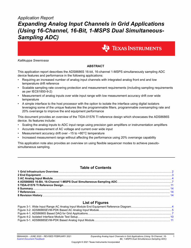
4 ADS8686S 16-Bit, 16-Channel 1-MSPS Dual Simultaneous-Sampling ADCThe ADS8686S is a 16-bit digital acquisition system (DAS) designed for a variety of generation, transmissionand distribution applications, including protection relays, terminal units (remote terminal units (RTU), distributionterminal units (DTU), and feeder terminal units (FTU), bay controller, merging unit and other grid applications.The ADS8688S device supports dual simultaneous sampling of input channels. The device can be configured toaccept ±10-V, ±5-V, or ±2.5-V bipolar inputs with a 20% overrange option using a single 5-V supply , whilesampling at throughput rates up to 1 MSPS with ≥90 dB SNR.
4.1 16 Channel Data Acquisition System (DAQ) for Grid Infrastructure Protection and PowerAutomation (8 × 2)Figure 4-1 shows the ADS8686S block diagram.
2.5V
VREF Buf
AVDD=5V
10��
PGAADC
DriverProg
LPF
AGND DGND
16-Bit SAR
ADC
ADS8686S
10��
16-Bit SAR
ADC
DVDD=3.3V
Typical 50-Hz, or 60-Hz
Sine-Wave from PT/CT
10��
PGAADC
DriverProg
LPF
10��
ALDO DLDO
9:1
Mu
ltip
lexe
r9
:1 M
ultip
lexe
r
Balanced RC Filter on
Each Input
R0AP
C0A
AIN_0AGND
AIN_0A
R0AM
R0BP
C0B
AIN_0BGND
AIN_0B
R0BM2:1
MU
XAVDD
ALDO
Figure 4-1. ADS8686S Based DAQ for Grid Applications
Some of the key features of the ADS8686S device follow:
• 16-channel, 16-bit ADC with integrated analog front-end• Dual simultaneous sampling: 8 × 2 channels• Supply:
– Analog: 5 V– Digital: 1.8 V to 5 V
• Constant 1-MΩ input impedance front-end• Independently programmable input ranges with 20% overrange• Programmable low-pass filter – 15 kHz, 39 kHz, 376 kHz• Excellent DC and AC performance• On-chip reference and reference buffer• Excellent temperature performance• Optional cyclic redundancy check (CRC) error checking• High-speed serial and parallel interfaces• Highly-configurable channel sequencer to reduce the sequencing overhead on the backend controller or
processor
www.ti.com ADS8686S 16-Bit, 16-Channel 1-MSPS Dual Simultaneous-Sampling ADC
SBAA442A – JUNE 2020 – REVISED FEBRUARY 2021Submit Document Feedback
Expanding Analog Input Channels in Grid Applications (Using 16-Channel, 16-Bit, 1-MSPS Dual Simultaneous-Sampling ADC)
7
Copyright © 2021 Texas Instruments Incorporated

ADC features users can use for performance improvements are discussed in the following sections:
4.1.1 Coherent and Simultaneous Sampling
CONVST (conversion start) is a logic input to control the conversion start for channel group A and channel groupB of the ADC. The rising edge of the CONVST pin, when BUSY is low, initiates a new conversion on the selectedinput channel pair from channel group A and channel group B. By controlling the CONVST timing based on theinput frequency and the number of required samples per cycle, coherent sampling can be achieved. Coherentsampling improves measurement accuracy by reducing the spectral leakage.
For normal mode and sequencer mode of operation, every CONVST signal performs one conversion of theselected channel pair based on the oversampling setting. For burst mode of operation only one CONVST signalis needed for the sequencer to cycle through the channel sequence. The BUSY signal is held high during thisduration.
In hardware mode, simultaneous sampling is restricted to the corresponding A and B channel (that is, channelAIN_0A is always sampled with channel AIN_0B). In software mode, any AIN_nA channel can be selected withany AIN_nB channel for simultaneous sampling.
4.1.2 Interface
A flexible digital interface supporting serial, parallel, and byte communication enables the device to be used witha variety of host controllers.
4.1.3 Diagnostics
The ADS8686S supports a CRC checksum mode to improve interface robustness by detecting errors in data.The CRC feature is available in both software (serial, byte, and parallel) mode and hardware (serial only) mode.
4.1.4 Accuracy
The ADS8686S can achieve Class 0.2 measurement accuracy because its on-chip ADCs have ≥90 dB of SNR.Higher SNR performance of ≥92 dB can be achieved by using the on-chip oversampling mode.
4.1.5 Simplicity
The ADS8686S is a 16-bit, DAS that supports dual simultaneous sampling of 16 channels. This input schemesimplifies system design by removing phase shift associated with voltage and current channels. In addition, itoperates from a single 5-V supply, which simplifies the power supply design.
4.1.6 Reduced System Cost
The ADS8686S is a 16-channel DAS that is highly integrated and can accept a variety of input signal ranges(±10 V, ±5 V, ±2.5 V) with 20% overrange. The analog front end features a 1-MΩ, high impedance, very low drift,input buffer. This eliminates the need for external protection circuits or external signal conditioning ICs, greatlyminimizing the system cost.
4.2 EnhancementsSome of the ADC features along with external buffers or TVS protection can be used for improving the systemperformance. Some of the enhancements are listed below:
4.2.1 Improving ADC Performance Using an Input Buffer
When the ADC input channels are left open or the sensor connected to the ADC input fails open, due to theinternal AFE structure a constant 2-V output is measured by the ADC. In grid applications where an output zeroduring sensor open conditioned is required, it is recommended to buffer the analog inputs using op amps. Theimplementation is discussed in the TI reference design: TIDA-010008 – Flat-Clamp TVS based ReferenceDesign for Protection Against Transient for Grid Applications .
4.2.2 Input Protection Using Flat-Clamp TVS
The ADC inputs are exposed to transients during normal operation and have to be protected. A TVS can isrecommended to protect the ADC inputs against transients. Use of flat-clamp TVS protects the analog inputsagainst overvoltage and transients. Refer TIDA-010008 – Flat-Clamp TVS based Reference Design forProtection Against Transient for Grid Applications for more details on using flat-clamp TVS for protection ofanalog inputs.
ADS8686S 16-Bit, 16-Channel 1-MSPS Dual Simultaneous-Sampling ADC www.ti.com
8 Expanding Analog Input Channels in Grid Applications (Using 16-Channel, 16-Bit, 1-MSPS Dual Simultaneous-Sampling ADC)
SBAA442A – JUNE 2020 – REVISED FEBRUARY 2021Submit Document Feedback
Copyright © 2021 Texas Instruments Incorporated

4.2.3 Achieving Pseudo-simultaneous Sampling by Using the ADS8686S Flexible Sequencer and BurstMode
In grid power systems protection and measurement applications, voltage and currents are sampledsimultaneously to minimize phase errors reducing the measurement error and compensation overheadsensuring faster and repeatable trip time characteristics.
Some applications implement instantaneous protections that require the phase voltages and currents to besampled simultaneously. Flexible sequencer and the burst mode options provided by the ADC can be used toachieve pseudo-simultaneous sampling.
4.2.3.1 Sequencer
The on-chip sequencer can be enabled to scan the channels in a preprogrammed manner. The SEQEN pin is adigital input pin that enables the internal channel sequencer mode for data capture in the hardware mode ofoperation. In the sequencer mode of operation, the CHSELx pins configure the settings for the sequencer. Thesequencer enables selection of the internal MUX connection in a predetermined order. This architecture helpsreduce the software overhead on the host controller to configure the next channel for conversion. A complete setof sequencer functionality and configurability is available in software mode. The sequencer stack has 32 uniqueconfigurable sequence steps. All channels, including the diagnostic channel, can be randomly programmed inany order. Additionally, any channel AIN_nA input can be paired with any channel AIN_nB input or diagnosticchannel. The sequencer can be operated with or without the burst function enabled. With the burst functionenabled, only one CONVST pulse is required to convert every channel in a sequence. With burst mode disabled,one CONVST pulse is required for every conversion step in the sequence.
In hardware mode, the sequencer has limited functionality. The sequencer always selects a particular channelpair (for example, AIN_nA and AIN_nB).
4.2.3.2 Burst Sequencer
The ADS8686S offers an additional feature for burst mode capture. This feature is applicable only if thesequencer feature is enabled. With the burst feature enabled, one CONVST pulse initiates conversion of allchannels configured in the sequencer. Thus, for a sequencer configured for four channel pairs, only oneCONVST pulse must be provided in BURST with the sequencer configuration instead of four CONVST pulses inthe sequencer-only configuration. The conversion results are presented on the data bus (parallel, byte, or serial)in the same order as the programmed sequence
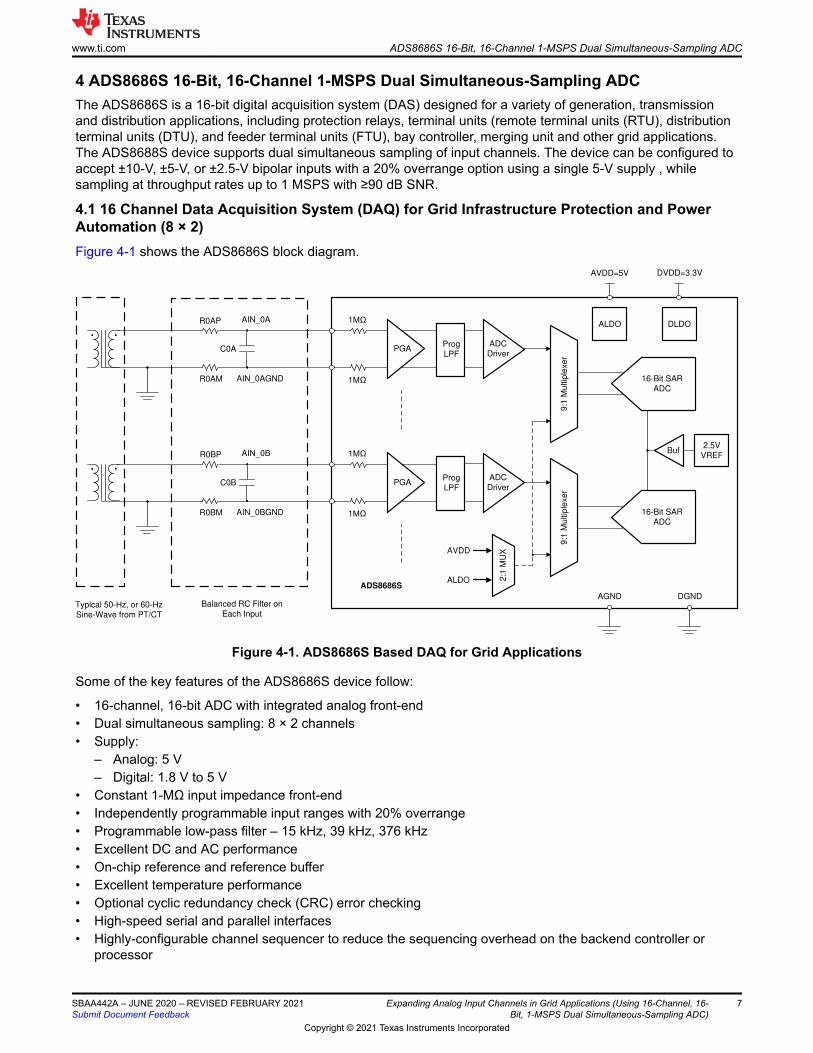
4.2.4 Isolated Interface
In HV transmission and MV distribution applications where the reliability of the secondary equipment is a criticalfactor for the overall system performance, the analog input module is isolated from the host. Use of digitalisolator simplifies the design and improved the reliability. The ADC is configured to interface with the host inserial mode and all the interface signals are isolated. Digital isolators with integrated power or digital isolatorswith external isolated DC/DC converters are used. Use of reinforced isolation increases system reliability.
Figure 4-2 shows the isolated interface module test setup showcased in TIDA-01576.
www.ti.com ADS8686S 16-Bit, 16-Channel 1-MSPS Dual Simultaneous-Sampling ADC
SBAA442A – JUNE 2020 – REVISED FEBRUARY 2021Submit Document Feedback
Expanding Analog Input Channels in Grid Applications (Using 16-Channel, 16-Bit, 1-MSPS Dual Simultaneous-Sampling ADC)
9
Copyright © 2021 Texas Instruments Incorporated
PHI
Controller
Board
PTS3.3
Voltage
And
Current
Source
TIDA-01576
AFE
ADS8686S
EVM-PDK
TIDA-01576Isolated
Interface
Board
SDCC
Connector
SDCC
Connector
Isolated
Supply
DC
Supply
ADS8686S EVM GUI
USB
Interface+5 V+5 V
Isolated Interface Module
Figure 4-2. Isolated Interface Module Test Setup
ADS8686S 16-Bit, 16-Channel 1-MSPS Dual Simultaneous-Sampling ADC www.ti.com
10 Expanding Analog Input Channels in Grid Applications (Using 16-Channel, 16-Bit, 1-MSPS Dual Simultaneous-Sampling ADC)
SBAA442A – JUNE 2020 – REVISED FEBRUARY 2021Submit Document Feedback
Copyright © 2021 Texas Instruments Incorporated

5 TIDA-01576 TI Reference DesignThe High accuracy analog input module reference design with 16-bit 1-MSPS dual simultaneous-sampling ADCfrom TI provides a solution for accurate measurement of 16-channel wide AC analog inputs (voltage and current)using precision 16-channel 16-bit 1-MSPS dual simultaneous-sampling ADC covering protection andmeasurement requirements (including sampling requirements as per IEC61850-9- 2) simplifying system design,improving trip time performance and reliability. Coherent sampling of the analog inputs with configurable samplesper cycle and programmable oversampling rate improves measurement performance. The reference designperformance has been tested over a wide temperature range with internal or external reference configured andno appreciable variation in error was observed.
The design showcases the design of an AC analog input module using the ADS8688S, 16-channel 16-bit 1-MSPS dual simultaneous-sampling ADC with integrated analog front-end.
Optionally, an isolated interface between ADS8686SEVM-PDK and the host PHI controller is showcased forimproved performance and safety in harsh operating conditions using a digital isolator with external isolatedDC/DC based power supply. No change in the ADC performance was observed.
For more information, see the TIDA-01576 High accuracy analog input module reference design with 16-bit 1-MSPS dual simultaneous-sampling ADC tool folder.
5.1 Test ResultsThe section provides details on the test setup and results for the ADS8686SEVM-PDK based analog inputmodule.
5.1.1 Test Setup
Figure 5-1 shows the test setup for testing the performance of the TIDA-01576 AFE interfaced to theADS8686SEVM-PDK.
PHI
Controller
Board
PTS3.3
Voltage
And
Current
Source
TIDA-01576
AFE
ADS8686S
EVM-PDK
SDCC
Connector
ADS8686S EVM GUI
+5 V
Non-Isolated Interface Analog Input Module
USB
Interface
DC Supply, E3631A
5.VDC, 200 mA
Figure 5-1. ADS8688SEVM-PDK Based Analog Input Module
A customized GUI was used for evaluating the TIDA-01576 TI reference design performance.
www.ti.com TIDA-01576 TI Reference Design
SBAA442A – JUNE 2020 – REVISED FEBRUARY 2021Submit Document Feedback
Expanding Analog Input Channels in Grid Applications (Using 16-Channel, 16-Bit, 1-MSPS Dual Simultaneous-Sampling ADC)
11
Copyright © 2021 Texas Instruments Incorporated

5.1.2 Voltage and Current Measurement Accuracy
Table 5-1 provides accuracy performance results for linear temperature variation. Measurements wereperformed by varying the input voltage and the minimum value, maximum value, and difference over a wideinput are summarized.
Table 5-1. Voltage and Current Measurement AccuracyTest Type Description ADC
Channel% Error Measured
Minimum Maximum DifferenceAccuracy testing with external referenceconfigured, 39-kHz filter
±10-V input range with 10 Vto 290 V input
5A –0.112 –0.032 0.080
5B –0.088 –0.011 0.077
6A –0.091 –0.007 0.084
6B –0.110 –0.032 0.078
±10-V input range with 10 Vto 360 V input
4A –0.144 –0.077 0.067
4B –0.191 –0.094 0.097
7A –0.188 –0.121 0.067
7B –0.138 –0.042 0.096
±10-V input range with 1 A to100 A input
4A –0.208 0.188 0.396
7B –0.206 0.188 0.394
±10-V input range with 1.95 Ato 165 A input
5A –0.217 0.209 0.427
6B 0.057 0.288 0.231
Accuracy testing with internal referenceconfigured, 39-kHz filter
±10-V input range with 10 Vto 290 V input
1A –0.077 0.023 0.100
1B –0.056 0.039 0.095
2A –0.056 0.042 0.097
2B –0.073 0.016 0.088
±10-V input range with 10 Vto 360 V input
0A –0.094 –0.005 0.090
0B –0.150 –0.053 0.096
3A –0.146 –0.051 0.095
3B –0.102 –0.005 0.097
Accuracy testing with external referenceconfigured, 15-kHz filter
±10-V input range with 10 Vto 290 V input
5A –0.104 –0.033 0.071
5B –0.080 –0.016 0.064
6A –0.084 –0.011 0.072
6B –0.102 –0.016 0.087
±10-V input range with 10 Vto 360 V input
4A –0.138 –0.046 0.092
4B –0.185 –0.094 0.091
7A –0.183 –0.091 0.091
7B –0.133 –0.041 0.092
TIDA-01576 TI Reference Design www.ti.com
12 Expanding Analog Input Channels in Grid Applications (Using 16-Channel, 16-Bit, 1-MSPS Dual Simultaneous-Sampling ADC)
SBAA442A – JUNE 2020 – REVISED FEBRUARY 2021Submit Document Feedback
Copyright © 2021 Texas Instruments Incorporated

5.1.3 Measurement Accuracy Drift Over Temperature
Table 5-2 provides accuracy results for linear temperature variation. Measurements were performed by varyingthe input voltage. The minimum value, maximum value, and difference over a wide input are summarized inTable 5-2.
Table 5-2. Variation in Measurement Accuracy Over TemperatureTest Type Input Voltage ADC
Channel% Error Measured
Minimum Maximum DifferenceAccuracy testing with external referenceconfigured and linear temperature variation in°C with ±10-V input range, 39 kHz filter 25,55, 80, 25, –15, 25
280 V 5A –0.121 –0.063 0.058
5B –0.096 –0.039 0.057
6A –0.093 –0.042 0.050
6B –0.119 –0.061 0.058
4A –0.147 –0.119 0.028
4B –0.194 –0.164 0.030
7A –0.191 –0.162 0.029
7B –0.142 –0.112 0.030
200 V 5A –0.112 –0.085 0.027
5B –0.086 –0.062 0.024
6A –0.089 –0.065 0.024
6B –0.108 –0.083 0.025
4A –0.133 –0.096 0.037
4B –0.180 –0.144 0.036
7A –0.179 –0.141 0.037
7B –0.129 –0.092 0.037
50 V 5A –0.070 –0.029 0.041
5B –0.047 –0.009 0.038
6A –0.047 –0.011 0.036
6B –0.069 –0.029 0.040
4A –0.102 –0.054 0.048
4B –0.150 –0.102 0.048
7A –0.143 –0.099 0.044
7B –0.097 –0.051 0.046
10 V 5A –0.043 –0.014 0.030
5B –0.026 –0.001 0.025
6A –0.026 0.009 0.035
6B –0.048 –0.023 0.025
4A –0.100 –0.062 0.038
4B –0.137 –0.116 0.020
7A –0.135 –0.098 0.037
7B –0.076 –0.041 0.035
www.ti.com TIDA-01576 TI Reference Design
SBAA442A – JUNE 2020 – REVISED FEBRUARY 2021Submit Document Feedback
Expanding Analog Input Channels in Grid Applications (Using 16-Channel, 16-Bit, 1-MSPS Dual Simultaneous-Sampling ADC)
13
Copyright © 2021 Texas Instruments Incorporated

6 SummaryUsing a 16-channel ADC simplifies AC analog input module design in applications requiring higher number ofanalog input channels or for increasing the dynamic range. The ADS8686S device is a dual simultaneous-sampling 16-channel, 16-bit ADC with configurable input ranges with 20% overrange. A flexible channelsequencer for sampling reduces software overhead. The ADS8686S has excellent accuracy performance overwide voltage inputs, current inputs and temperature range.
7 ReferencesReferences used in this application note is listed below:
• Texas Instruments, ADS8686S, 16-channel 16-bit 1-MSPS dual simultaneous-sampling ADC with integratedanalog front end (AFE) product folder
• Texas Instruments, ADS8686S 16-channel 16-bit 1-MSPS dual simultaneous-sampling ADC performancedemonstration kit (PDK) ADS8686SEVM-PDK
• Texas Instruments, Isolated power architecture reference design for communication and analog input/outputmodules
• Texas Instruments, Non-isolated power architecture with diagnostics reference design for protection relaymodules
• Texas Instruments, Flat-Clamp TVS based Reference Design for Protection Against Transient for GridApplications
• Texas Instruments, High-efficiency, low-emission, isolated DC/DC converter-based analog input modulereference design
• Texas Instruments, Introduction to HVDC Architecture and Solutions for Control and Protection ApplicationReport
8 Revision HistoryNOTE: Page numbers for previous revisions may differ from page numbers in the current version.
Changes from Revision * (June 2020) to Revision A (February 2021) Page• Updated the numbering format for tables, figures and cross-references throughout the document...................2
Summary www.ti.com
14 Expanding Analog Input Channels in Grid Applications (Using 16-Channel, 16-Bit, 1-MSPS Dual Simultaneous-Sampling ADC)
SBAA442A – JUNE 2020 – REVISED FEBRUARY 2021Submit Document Feedback
Copyright © 2021 Texas Instruments Incorporated

IMPORTANT NOTICE AND DISCLAIMERTI PROVIDES TECHNICAL AND RELIABILITY DATA (INCLUDING DATASHEETS), DESIGN RESOURCES (INCLUDING REFERENCEDESIGNS), APPLICATION OR OTHER DESIGN ADVICE, WEB TOOLS, SAFETY INFORMATION, AND OTHER RESOURCES “AS IS”AND WITH ALL FAULTS, AND DISCLAIMS ALL WARRANTIES, EXPRESS AND IMPLIED, INCLUDING WITHOUT LIMITATION ANYIMPLIED WARRANTIES OF MERCHANTABILITY, FITNESS FOR A PARTICULAR PURPOSE OR NON-INFRINGEMENT OF THIRDPARTY INTELLECTUAL PROPERTY RIGHTS.These resources are intended for skilled developers designing with TI products. You are solely responsible for (1) selecting the appropriateTI products for your application, (2) designing, validating and testing your application, and (3) ensuring your application meets applicablestandards, and any other safety, security, or other requirements. These resources are subject to change without notice. TI grants youpermission to use these resources only for development of an application that uses the TI products described in the resource. Otherreproduction and display of these resources is prohibited. No license is granted to any other TI intellectual property right or to any third partyintellectual property right. TI disclaims responsibility for, and you will fully indemnify TI and its representatives against, any claims, damages,costs, losses, and liabilities arising out of your use of these resources.TI’s products are provided subject to TI’s Terms of Sale (https:www.ti.com/legal/termsofsale.html) or other applicable terms available eitheron ti.com or provided in conjunction with such TI products. TI’s provision of these resources does not expand or otherwise alter TI’sapplicable warranties or warranty disclaimers for TI products.IMPORTANT NOTICE
Mailing Address: Texas Instruments, Post Office Box 655303, Dallas, Texas 75265Copyright © 2021, Texas Instruments Incorporated