analog applications journal - texas instruments · analog applications journal is a collection of...
TRANSCRIPT

Texas Instruments Incorporated
Analog and Mixed-Signal Products
Analog ApplicationsJournal
First Quarter, 2004
© Copyright 2004 Texas Instruments

Texas Instruments Incorporated
2
Analog Applications JournalAnalog and Mixed-Signal Products www.ti.com/sc/analogapps 1Q 2004
IMPORTANT NOTICE
Texas Instruments Incorporated and its subsidiaries (TI) reserve the right to make corrections, modifications,enhancements, improvements, and other changes to its products and services at any time and to discontinueany product or service without notice. Customers should obtain the latest relevant information before placingorders and should verify that such information is current and complete. All products are sold subject to TI’s termsand conditions of sale supplied at the time of order acknowledgment.
TI warrants performance of its hardware products to the specifications applicable at the time of sale inaccordance with TI’s standard warranty. Testing and other quality control techniques are used to the extent TIdeems necessary to support this warranty. Except where mandated by government requirements, testing of allparameters of each product is not necessarily performed.
TI assumes no liability for applications assistance or customer product design. Customers are responsible fortheir products and applications using TI components. To minimize the risks associated with customer productsand applications, customers should provide adequate design and operating safeguards.
TI does not warrant or represent that any license, either express or implied, is granted under any TI patent right,copyright, mask work right, or other TI intellectual property right relating to any combination, machine, or processin which TI products or services are used. Information published by TI regarding third–party products or servicesdoes not constitute a license from TI to use such products or services or a warranty or endorsement thereof.Use of such information may require a license from a third party under the patents or other intellectual propertyof the third party, or a license from TI under the patents or other intellectual property of TI.
Reproduction of information in TI data books or data sheets is permissible only if reproduction is withoutalteration and is accompanied by all associated warranties, conditions, limitations, and notices. Reproductionof this information with alteration is an unfair and deceptive business practice. TI is not responsible or liable forsuch altered documentation.
Resale of TI products or services with statements different from or beyond the parameters stated by TI for thatproduct or service voids all express and any implied warranties for the associated TI product or service andis an unfair and deceptive business practice. TI is not responsible or liable for any such statements.
Mailing Address:
Texas InstrumentsPost Office Box 655303Dallas, Texas 75265

Texas Instruments Incorporated
3
Analog Applications Journal 1Q 2004 www.ti.com/sc/analogapps Analog and Mixed-Signal Products
Introduction . . . . . . . . . . . . . . . . . . . . . . . . . . . . . . . . . . . . . . . . . . . . . . . . . . . . . . . . . . . . . . . 4
Data AcquisitionTwo-channel, 500-kSPS operation of the ADS8361 . . . . . . . . . . . . . . . . . . . . . . . . . . . . . . 5
Texas Instruments Application Report SLAA164 presented a basic method of interfacing the ADS8361to the TMS320C6711TM DSP Starter Kit. The purpose of this article is to expand on the fundamentalspresented in that application report and to explore 2- and 4-channel operation of the ADS8361 with twomultichannel buffered serial ports (McBSPs). The information presented in this article can be applied toany TMS320TM series DSP with two or more McBSPs.
ADS809 analog-to-digital converter with large input pulse signal . . . . . . . . . . . . . . . . . 8The ADS809 is a 12-bit, 80-MHz analog-to-digital converter that offers many performance features usinga uniform or non-uniform clock. This article explores over-range and input step-response performanceof the ADS809, including bench test data.
Power ManagementLED-driver considerations. . . . . . . . . . . . . . . . . . . . . . . . . . . . . . . . . . . . . . . . . . . . . . . . . . . 14
Many portable applications require backlight LED-driver solutions. This article covers various LED-driver techniques and typical circuit examples for current control, PWM dimming, overvoltageprotection, and evaluating load disconnects.
InterfaceEstimating available application power for Power-over-Ethernet applications . . . . . 18
The recently approved IEEE 802.3af Power-over-Ethernet standard is gaining wide industry acceptance.The application designer is faced with a need both to simplify power delivery to the application and tolimit how much power is available to the application’s functional circuits. This article discusses thereality of how much power is available and tools to maximize it.
The RS-485 unit load and maximum number of bus connections . . . . . . . . . . . . . . . . . 21The TIA/EIA-485 (RS-485) standard defines a unit load and confines bus configurations to 32. Thisarticle explains the unit-load concept and how it relates to the maximum number of bus connections.Fractional unit-load devices, such as the 1/8-unit-load SN65HVD21 and SN65HVD06, allow up to 256devices on a single bus segment.
Amplifiers: Op AmpsOp amp stability and input capacitance . . . . . . . . . . . . . . . . . . . . . . . . . . . . . . . . . . . . . . . 24
This article explores the effects of capacitance on stability in both internally compensated andexternally compensated amplifiers.
Integrated logarithmic amplifiers for industrial applications . . . . . . . . . . . . . . . . . . . . . 28This article describes the operation and architecture of integrated log amps and provides twoapplication examples using the LOG112 and LOG2112.
Index of Articles. . . . . . . . . . . . . . . . . . . . . . . . . . . . . . . . . . . . . . . . . . . . . . . . . . . . . . . . . . 33
TI Worldwide Technical Support . . . . . . . . . . . . . . . . . . . . . . . . . . . . . . . . . . . . . . . . . . 36
Contents
To view past issues of theAnalog Applications Journal, visit the Web site
www.ti.com/sc/analogapps

Texas Instruments Incorporated
4
Analog Applications JournalAnalog and Mixed-Signal Products www.ti.com/sc/analogapps 1Q 2004
Analog Applications Journal is a collection of analog application articlesdesigned to give readers a basic understanding of TI products and to providesimple but practical examples for typical applications. Written not only fordesign engineers but also for engineering managers, technicians, systemdesigners and marketing and sales personnel, the book emphasizes generalapplication concepts over lengthy mathematical analyses.
These applications are not intended as “how-to” instructions for specificcircuits but as examples of how devices could be used to solve specific designrequirements. Readers will find tutorial information as well as practicalengineering solutions on components from the following categories:
• Data Acquisition
• Power Management
• Interface
• Amplifiers: Op Amps
Where applicable, readers will also find software routines and programstructures. Finally, Analog Applications Journal includes helpful hints andrules of thumb to guide readers in preparing for their design.
Introduction
Introduction

5
Analog Applications Journal
IntroductionThe ADS8361 is a member of the Texas Instruments (TI)motor control products family of serial analog-to-digitalconverters (ADCs). The ADS8361 is a 2+2-channel, 16-bitupgrade for the 2+2-channel, 12-bit ADS7861. Its 3.3- to5-V digital interface is ideally suited for use with the entireTMS320 series of digital signal processors from TI.
The device features two independent 500-kSPS ADCchannels, each with its own sample-and-hold circuits andserial data output pin. A user-controllable multiplexer(MUX) allows simultaneous sampling of two 2-channelpairs (4 total channels) at 250 kSPS.
Hardware pinsThe ADS8361 features three hardware pins (M0, M1, andA0) that select various operating modes (see Table 1).
Mode I allows for 2-channel operation at speeds of up to500 kSPS by utilizing both conversion channels. Mode IIreduces the maximum throughput to 250 kSPS by using asingle serial output pin (OUTA) to present the simultane-ously sampled data from channel pairs Ax and Bx. Togglingthe address pin A0 controls the selection of channel pair 0or 1.
Modes III and IV allow the sequential output of bothsimultaneously sampled channel pairs A0 and B0, followedby A1 and B1. Since Mode III uses both serial outputs Aand B, the maximum throughput can be maintained at 250kSPS. Mode IV presents all 4 converted channels at theOUTA pins, with a maximum throughput of 125 kSPS.
Single McBSP operationWith the interface method presented in Reference 1, appli-cations that do not require simultaneous sampling but doneed two fast, independent ADCs can benefit from theADS8361’s 2-µs conversion time. An external MUX or bus
Texas Instruments Incorporated Data Acquisition
By Tom Hendrick (Email: [email protected])Data Acquisition Applications
1Q 2004 www.ti.com/sc/analogapps Analog and Mixed-Signal Products
switch between the serial outputs would allow 1- to 4-channel operation of channel A or B through a single multichannel buffered serial port (McBSP). Each channelcan be independently operated at 500 kSPS. This methodwould require some sort of control over the state of one ormore of the hardware pins M0, M1, and A0, adding addi-tional logic to the design.
Applications with 2 channels and simultaneous-samplingrates of 250 kSPS or less also can use a single McBSP.Hardware pins M0 and M1 can be fixed at ground and VCC,with A0 controlling the channel pairs to be converted(Mode II). This method uses the internal MUX to switchthe conversion results from the A and B channels throughOUTA. Tying both M0 and M1 to VCC permits 4-channel,simultaneous-sampling applications to be realized. It alsoallows sequential presentation of two simultaneously sampled channel pairs, 4 channels in all (Mode IV), forapplications needing sampling rates of 125 kSPS or less.
If a second McBSP is available, 2- and 4-channel, simultaneous-sampling operation can be realized with noadditional “glue logic” required, at 500-kSPS throughputper channel for 2 channels and 250-kSPS for 4 channels.
Dual McBSP operationThe simultaneous conversion properties of the ADS8361allow conversion data from channels Ax and Bx to be pre-sented to the OUTA and OUTB pins at the same time.Both channels use the same conversion start (CONVST)signal and the same conversion clock so that data skewbetween A and B outputs is minimized.
To achieve full-speed, 2- and 4-channel operation, thetransmitter portion (CLKX, FSX and DX lines) of oneMcBSP can be used to control the conversion speed, tim-ing, and channel selection of the ADS8361. The ADS8361’sserial data outputs, along with clock and frame sync
Two-channel, 500-kSPS operation of the ADS8361
DATA ON TOTALMODE HARDWARE PINS 2-CHANNEL/ SERIAL CHANNELS THROUGHPUT
M0 M1 A0 4-CHANNEL OPERATION OUTPUTS CONVERTED (kSPS)0 0 0 2-channel A and B A0 and B0 500
I 0 0 1 2-channel A and B A1 and B1 5000 1 0 2-channel A only A0 and B0 250
II 0 1 1 2-channel A only A1 and B1 250III 1 0 X 4-channel A and B Sequential 250IV 1 1 X 4-channel A only Sequential 125
Table 1. Operating modes of ADS8361 hardware pins

Texas Instruments IncorporatedData Acquisition
6
Analog Applications JournalAnalog and Mixed-Signal Products www.ti.com/sc/analogapps 1Q 2004
return, are then fed to the receiver portions of twoMcBSPs as shown in Figure 1.
To enhance the control of the ADS8361 further,the unused transmitter section of the second McBSPcan be configured as GPIO and connected to thecontrol pins M0, M1, and A0 of the ADS8361. Forsimultaneous, 2-channel operation at a 500-kSPS-per-channel conversion rate, all that is required is asingle GPIO line to toggle A0.
Software interfaceA project database for this article was developedand compiled with Code Composer StudioTM version2.20. The most involved portion of writing the codefor this simple interface was programming theMcBSP. If you wish to receive the project file used inthis example, please feel free to send an email [email protected] with the title of this articleas the subject.
Since the two converters in the ADS8361 share acommon interrupt, conversion clock, and conversion startmechanism, the software requirements for the DSP arequite simple. The first McBSP is configured to transmit aframe sync pulse to act as the conversion start signal. FSRA,DXA (Serial Data A), and CLKRA are returned to the firstMcBSP. The ADS8361’s BUSY pin acts as an interrupt to theDSP, which in turn reads the serial data. When the secondserial output of the ADS8361 is used, FSR, CLKR, and SerialOUTB are returned to the receiver of the second McBSP.This enables the user to configure the transmitter portionas GPIO to control channel 0 or channel 1 selection of theADS8361 without the use of additional decode circuits.
Create a .CDB fileCode Composer Studio’s graphical user interface for theDSP/BIOSTM configuration (.CDB file) and Chip SupportLibraries (CSL) have made it easier than ever to writeprograms and set up the McBSP.
The first step in creating a project that accommodatesthe ADS8361 with two McBSPs is to create a .CDB file,then add it to the project. This process creates a .CMD filefor the linker, which also needs to be added to the project.Additional DSP/BIOS files are created too, which are addedto the project automatically when the .CDB file is loaded.All necessary files and libraries are loaded automatically,
based on the DSP/BIOS configurationoptions set.
By expanding the CSL tab in the .CDBfile, the user gains access to the McBSPConfiguration Manager. A McBSP con-figuration is added, and the desired values for clock speed, etc., are set.Once the first configuration is done, it issimply highlighted, copied, and pasted.This creates two copies of the sameconfiguration, each with its own name.
McBSP settingsThe McBSPs are configured as shown inthe sidebar at left.
The McBSP is programmed as a serialport in nonstop clock mode (or DSPmode). Frame sync and serial clock sig-nals are output pins. The receiver is setfor 16-bit transfers with a 2-bit delay ondata receive. The frame sync (FSX1) isgenerated by the sample-rate generatorand is used for both the RD—– and CONVSTsignals on the ADS8361 by jumper W2on the evaluation module (EVM).
ADS8361TMS320C54xx/
C67xx
BVDD
Serial Data A DRA
Serial Data B DRB
CONVST FSXA
FSRA
FSRB
CLKXA
CLKRA
CLKRB
Clock
M1
M0
CS
RD
Figure 1. Hardware interface example
MCBSP_Config mcbspCfg0 = 0x0000, /* Serial Port Control Register 1 */0x0220, /* Serial Port Control Register 2 */0x0060, /* Receive Control Register 1 */0x0000, /* Receive Control Register 2 */0x0060, /* Transmit Control Register 1 */0x0005, /* Transmit Control Register 2 */0x0109, /* Sample Rate Generator Register 1 */0x3014, /* Sample Rate Generator Register 2 */0x0000, /* Multichannel Control Register 1 */0x0000, /* Multichannel Control Register 2 */0x2a00, /* Pin Control Register */
;MCBSP_Config mcbspCfg1 =
0x0000, /* Serial Port Control Register 1 */0x0200, /* Serial Port Control Register 2 */0x0060, /* Receive Control Register 1 */0x0000, /* Receive Control Register 2 */0x0000, /* Transmit Control Register 1 */0x0000, /* Transmit Control Register 2 */0x010e, /* Sample Rate Generator Register 1 */0x3013, /* Sample Rate Generator Register 2 */0x0000, /* Multichannel Control Register 1 */0x0000, /* Multichannel Control Register 2 */0x0a00, /* Pin Control Register */
;

Texas Instruments Incorporated Data Acquisition
7
Analog Applications Journal 1Q 2004 www.ti.com/sc/analogapps Analog and Mixed-Signal Products
In the sample code (see sidebar), the ADS8361is running at 469 kSPS with a serial clock of 9.375 MHz. The C6711 DSP Starter Kit clocks theC6711 DSP at 150 MHz. The sample-rate genera-tor clock source is half the CPU clock, or 75 MHz.The 9.4-MHz clock on CLKX is achieved by settingthe CLKGDV bit field in the sample-rate genera-tor register to 8. The formula for calculating theserial clock is
By this equation, each clock’s cycle is approxi-mately 106.6 ns, triggering a frame-sync pulseevery 20 serial clock cycles, which gives a samplerate of 468 kHz. The frame period (FPER) field,in the sample-rate generator register, is where the20-cycle period is set.
Software flowThe software presented in this article reads 1024samples at 469 kHz continuously. As selected inthe configuration tool, all the register and periph-eral programming is done during initialization.DSP/BIOS pre-initializes all the McBSP registers and otherDSP registers before arriving in the main function. As aresult, the main function simply enables the interrupt service routine and McBSP1; from then on, the DSP/BIOSand McBSP receive ISR do all the work. When a McBSP1receive interrupt occurs, McBSP1Rcv_ISR reads the portand stores the data in ad_buffer. When the buffer isfull, it resets the index, i, to the beginning and flushes thereceive buffer (see Figure 2).
ConclusionAn EVM is available that provides a platform to demon-strate the functionality of the ADS8361 ADC with variousTI DSPs and microcontrollers, while allowing easy accessto all analog and digital signals for customized end-userapplications. For more information on the EVM, visitwww.ti.com/sc/device/ADS8361 and selectDevelopment Tools.
CLOCK
CPUCLOCK
CLKDIV=
+2
1.
ReferencesFor more information related to this article, you can down-load an Acrobat Reader file at www-s.ti.com/sc/techlit/litnumber and replace “litnumber” with the TI Lit. # forthe materials listed below.
Document Title TI Lit. #
1. Tom Hendrick, “Interfacing the ADS8361 to the TMS320C6711 DSP,” Application Report . .slaa164
2. “Dual, 500kSPS, 16-Bit, 2 + 2 Channel, Simultaneous Sampling Analog-to-Digital Converter,” ADS8361 Data Sheet . . . . . . . . . . . .sbas230
3. “TMS320C6711, TMS320C6711B, TMS320C6711C Floating-Point Digital SignalProcessing,” Data Sheet . . . . . . . . . . . . . . . . . . . .sprs088
4. “TMS320C6000 DSP/BIOS User’s Guide” . . . . . .spru3035. “TMS320 Cross-Platform Daughtercard
Specification, Revision 1.0,” Application Report . . . . . . . . . . . . . . . . . . . . . . . .spra711
Related Web sitesanalog.ti.com
www.ti.com/sc/device/partnumber
Replace partnumber with ADS7861, ADS8361 orTMS320C6711
Read DRR1Store Sample in ad_buffer
Set DSPEnable Interrupt (RINT1)
Start McBSP1
Main ( )
Reset Pointer andFlush Receive
Buffers
Return from ISR
ad_buffer full?N
Y
Interrupt Service RoutineMcBSP1Rcv_ISR( )
Figure 2. Software flow chart

8
Analog Applications JournalAnalog and Mixed-Signal Products www.ti.com/sc/analogapps 1Q 2004
ADS809 analog-to-digital converter with large input pulse signal
IntroductionThe Texas Instruments (TI) ADS809 is a 12-bit, 80-MHzpipeline analog-to-digital converter (ADC). It has highspeed, high resolution, high-input bandwidth, and a highsignal dynamic range. Its many other good features includegood signal-to-noise-ratio (SNR), good linearity, low jitter,flexible clocking, an over-range indicator (OVR), “datavalid” output, three-state output, an internal or externalreference, and a single-ended or differential input configu-ration. It can be used for broadband communications, testequipment, medical instrumentation, CCD imaging, andother fast-ADC applications.
In these applications the input analog signal applied tothe ADS809 varies and may be a DC, AC, narrow band, wideband, or pulse signal with a large amplitude. The samplingclock used for these applications can be up to 80 MHz witha uniform or non-uniform clock phase. Different applica-tions require different critical features of the ADS809. Insome conventional sampling applications, the ADC inputanalog signal is smooth with a large amplitude, and theSNR and spurious-free dynamic range (SFDR) are critical;while in some small-signal sampling applications, the SFDRand full-scale (FS) step-acquisition time are not as critical.However, the FS step-acquisition time is critical in large-signal sampling applications, especially when the samplingclock has to be high-frequency with a non-uniform phaseand the analog input pulse signal is large (for example, 2 V).In this case the input signal has a sharp edge with a largevoltage amplitude, and the pulse edge could be very close
to the sampling clock edge due to sampling clock phasevariations. If the ADC does not have fast step response forthe signal settling, the next ADC sample after the pulseedge will be unstable, which is undesirable. Therefore it iscritical for the ADC to have a fast settling time when alarge input pulse signal is sampled. Similarly, when theinput pulse is over full-scale range (FSR), it is importantfor the ADC to have a fast over-range recovery time. Thisis tough for any ADC in applications where the input pulsesignal is large and sampling speed is very high with a non-uniform clock phase. However, the ADS809 works well withthis type of application. This article presents the results ofrecent lab tests that further prove the ADS809’s fast stepresponse with a large, FS input pulse. The test data alsocovers the ADS809’s response to over-range conditions.
Over-FSR performance of the ADS809The ADS809’s over-voltage condition is defined as theinput voltage in excess of its maximum linear conversionrange. The voltage FSR of the ADS809 can be set as 2 Vp-p,1.5 Vp-p, 1 Vp-p, or another range based on the internal orexternal voltage reference configuration. For single-endedinput, the maximum voltage at the ADS809 input pin is+FS (1/2 FSR above 2.5-V common-mode voltage), and theminimum voltage at input is –FS (1/2 FSR below 2.5-V common-mode voltage). For differential input, +FS is 1/4FSR above 2.5-V common-mode voltage, and –FS is 1/4 FSRbelow 2.5-V common-mode voltage. For the input voltageover FSR, the ADS809 has control features that include12-bit data-code control and an OVR.
Texas Instruments IncorporatedData Acquisition
By Hui-Qing Liu (Email: [email protected])Applications Engineer, High-Speed Products
Number of Samples
Dig
italO
utp
ut
Valu
e
4000
3500
3000
2500
2000
1500
1000
500
0
–5000 50 100 150 200 250
Figure 1. Output of ADS809 with input pulse over FSR at 66-MHz sampling clock

Texas Instruments Incorporated Data Acquisition
9
Analog Applications Journal 1Q 2004 www.ti.com/sc/analogapps Analog and Mixed-Signal Products
The digital output code of the ADS809 is straight offsetbinary or binary two’s complement. In straight offset binaryformat, when the input voltage is maximum, the ADS809outputs all 12 data bits as 1s (digital value = 4095); andwhen the input voltage is minimum, the ADS809 outputsall 0s. When the input voltage is 0 (at the middle of theFSR) or only the common-mode voltage, the ADS809 outputs 100000000000 (digital value = 2048). The ADS809will output data from 0 to 4095 when the input voltage isfrom –FS to +FS – LSB. The ADS809 will output 4095when the input voltage is above +FS, and will output 0when the input voltage is below –FS.
The ADS809 output-code control was tested with theADC sampling clock at 66 MHz and the input differentialpulse amplitude at 2.8 V (0.8 V over FSR). The test resultshows that the ADS809 has stable output-code control andquick over-range recovery from the input pulse signal.This is shown in Figure 1. The ADS809 samples 255 digitaloutput samples at 66 MSPS from an over-FS input pulse.The data shows that all the bits are stable at 1 when theinput pulse signal is over +FS, and stable at 0 when theinput pulse signal is under –FS. The data also shows thatwhen the input pulse signal goes from over FS to underFS or vice versa, the output of the ADS809 tracks theinput step change and stays at 4095 or 0 without any misscode or bit flip.
Another over-FSR control feature of the ADS809 is anOVR output pin, which indicates over-range conditions.The OVR output is a function of the reference voltage and
the output data bits, so it has the same pipeline delay asthe output data bits. The OVR is logical low if the inputsignal is within the FSR, and logical high if the input signalis over +FS or under –FS. The OVR changes from logicallow to high, or logical high to low, immediately followingthe change of the output data. When this happens, theinput voltage changes from inside the FSR to outside theFSR or vice versa. When the input signal continues underor over FS, the OVR always remains high. When the inputsignal changes from under FS to over FS or vice versa, theOVR changes from high to low for 1/2 CLK period, thenchanges to high again. In other words, the OVR outputs anegative pulse at the transition of the input voltage fromover FS to under FS or vice versa (see Figure 2). The output’s most significant bit (MSB) pin is flipped based onthe over-FS input pulse. It is high when the input pulse isover FS and low when the input pulse is under FS. TheOVR pin outputs a negative pulse that appears half of thesampling clock period earlier than the transition at theMSB pin.
FS step response of ADS809 and measurement methodThe FS step response or step-acquisition time of theADS809 is defined as the time for the input signal to settleor for the internal sample-and-hold (S/H) circuit to trackthe input signal with a certain accuracy (for example,0.1% FS) after the FS step signal is applied to the ADS809.The ADS809 settling time of a FS step signal is 5 ns, which
is typically within 0.1% FS andis the minimum required inter-val between the input stepedge and the next samplingclock edge.
The fast step response ofthe ADC is important in appli-cations with a non-uniformsampling clock, because thevariation of the sampling clockphase can cause a phase changebetween the input pulse andthe sampling clock. This isshown in Figure 3, where therising edge of the clock samplesthe input pulse signal; and thetime, tS, between the input stepedge and the next rising edgeof the sampling clock changeswith the sampling clock phasechange. When tS is less thanthe ADC’s minimum value, theADC will take an unstable sam-ple from the unsettled inputsignal, which is undesirable.
SamplingCLK
(66 MHz)
Differential Input Amplitude = 2.8 VFrequency = 3.3 MHz
MSB
OVR
Figure 2. OVR of ADS809 with input pulse over FS
CLK
tS tS
tS
InputPulse
Figure 3. The input step appears during the clock’s tracking timebecause of clock phase variation

Texas Instruments IncorporatedData Acquisition
10
Analog Applications JournalAnalog and Mixed-Signal Products www.ti.com/sc/analogapps 1Q 2004
There are two ways to eval-uate the step response. One ismeasuring the time, tS, shownin Figure 3. Another is measur-ing the relative tracking time,tD, of the sampling clockshown in Figure 4.
In the first method, the stepsignal (pulse edge in this case)is applied to the input of theS/H circuit directly during thetracking phase. By delayingthe input pulse or sampling clock, we can find the minimumtS, the first stable sample location after the pulse edge,where the pulse signal level has been recovered with theaccuracy specified in the data sheet. This minimum tS isthe step response of the ADC. In this method, highly accu-rate measurement is needed. The signal input path of theADC should be clean. Large external input capacitancefrom the board can cause signal step edge distortion, andpoor board layout with source impedance mismatch maycause energy reflection or ringing. The probe capacitanceof the oscilloscope is also a concern. The shape of the stepedge and the detailed timing between the step signal andthe ADS809 sampling clock should be carefully measured,including the ADS809 aperture time.
The second and simpler method of step-response evalu-ation is to measure the clock’s tracking time, tD, shown inFigure 4. In this method the clock’s tracking edge appearsafter the input signal step edge. The clock’s tracking edgetriggers the ADS809 S/H circuit, changing the previousvoltage at the sampling capacitor to the current voltage ofthe input pulse. The step-response time of the ADS809 S/Hcircuit should be the same as in the first method (measur-ing tS) due to the same RC constant. If the tracking timeduring tD measurement is too short, the first sample afterthe step signal will be unstable. The minimum tracking
time of the ADC should be less than or close to half of thesampling clock cycle at the maximum speed specified.
Bench test of ADS809 step responseA real bench test was performed to determine the ADS809step response with the method shown in Figure 3 (measur-ing tS). The basic test block diagram of the ADS809 is shownin Figure 5. The ADS809 was configured with an internalreference, a differential analog input with 2-V FSR, a differ-ential clock input, and an external 2.5-V common-modevoltage for the analog input, with no added load on thecommon-mode (CM) pin except normal bypass capacitance.
The differential analog input of the ADS809 was a pulsefrom the pulse generator with a frequency of 3.3 MHz andan amplitude of 2.92 to 2.08 V (high to low) at each analoginput, near FSR. This input produced the digital outputvalues of 3770 and 300 (high and low), including a smallamount of DC offset. The input pulse’s transition from highto low was used as the step signal in the bench test. Thesingle-ended, 66-MHz sampling clock from the pulse genera-tor was converted differentially through a differential trans-lator. A Tektronix logic analyzer (TLA) was used to collectthe digital output of the ADS809 to determine whether thesample was stable. After the input step signal, the digitalvalue of the first sample should be 300, within an accuracy
CLK
tD tDInputPulse
Figure 4. The input step does not appear during the clock’s tracking time
25 Ω
25 Ω
50 Ω
0.1 µF0.1 µF
12-bit
D
Q –Q
ADS809EVM
IN
–IN
–CLKCLK
Pulse Generator
TLA50 Ω
50 Ω
Figure 5. Basic test block diagram for ADS809 step response

Texas Instruments Incorporated Data Acquisition
11
Analog Applications Journal 1Q 2004 www.ti.com/sc/analogapps Analog and Mixed-Signal Products
of 0.1% FS, if the time interval betweenthe step signal and the clock samplingedge is 5 ns or more as specified.
Three measurements were necessary inthis bench test: aperture delay; input sig-nal timing between the sampling clock andthe input pulse; and the digital output ofthe ADS809 with input pulse delay.
The aperture delay, tA, is the time fromthe rising edge of the sampling clock to thetime when the sampling actually happens (see Figure 6).The data sheet provides only a typical value for tA (3 ns).In the bench test the aperture delay was found by mea-suring the MSB and the time from the rising edge of thesampling clock to the falling edge of the pulse.
Figure 6 shows the measurement of the input signaltiming between the sampling clock and the input pulse atzero delay. This measurement provides pulse edge infor-mation and a time reference for the input signal delay. Themeasurement was taken by Tektronix scope at the ADS809input and clock input pins. The measurement data isshown in Table 1.
After the input timing was measured, the input pulsedelay, tDel, was up to 12 ns in steps of 1 ns or less. WhentDel was 0, the time from the input pulse falling edge tothe next rising edge of the sampling clock, tFR, was 6.59 ns;and Sample A, the first sample after the high-to-low transition of the input pulse, was located at 9.59 ns (tFR + tA = tFA) from the pulse falling edge (see Figure 6).With the increase of the input pulse delay, tFR decreasedand Sample A moved close to the falling edge of the inputpulse. When the pulse delay was more than 9.5 ns, Sample A moved to the left side of the falling edge of the input pulse (see Figure 7).
PARAMETER MEASURED VALUEInput pulse rising time (10% to 10%), tPR1 1.1 ns at analog input pin INInput pulse falling time (10% to 10%), tPF1 0.8 ns at analog input pin INInput pulse rising time (0.01% to 0.01%), tPR2 2.7 ns at analog input pin INInput pulse falling time (0.01% to 0.01%), tPF2 2.8 ns at analog input pin INClock rising edge to pulse rising edge (50% to 50%), tRR 8.5 ns at pins CLK and INPulse falling edge to clock rising edge (50% to 50%), tFR 6.59 ns at pins CLK and IN
Table 1. Bench test measurement data
tPR1
tRR
tPF1
tFR
tFA
Sample A
tA
tPR2 tPF2
SamplingCLK
Input Pulse
Figure 6. Timing measurement of sampling clock and input pulse at zero delay
Actual Sampling Edge
Input Step Delay, t = 0 nsDel
t = 6 nsDel
t = 9.6 nsDel
t = 12 nsDel
Sample A
Figure 7. Sample A moves with step signal delay

Texas Instruments IncorporatedData Acquisition
12
Analog Applications JournalAnalog and Mixed-Signal Products www.ti.com/sc/analogapps 1Q 2004
Sample A was collected by TLA, and its digital data isshown in Table 2. The Sample A output value of theADS809 should be 300 (within an accuracy of ±0.1% FS)if tFR is 2 ns or longer. In other words, Sample A is settledif the time tFA (tFR + tA), from the falling edge of the inputpulse to the actual sampling time of Sample A, is 5 ns orlonger. For example, the digital value of Sample A is 299when tFA is 5.59 ns, and 300 when tFA is about 9.59 ns, dueto the input signal tracked by the ADS809 at these times.Sample A is unstable (the digital value is out of the rangeof 300 ± 0.1% FS) if tFA is shorter than 5 ns. This is shownin Table 2 and Figure 8. For example, when tFA is 3.59 ns,the digital value of Sample A is 358, which is significantlyhigher than 300, because the input signal has not recoveredits low level after the high-to-low step of the input pulse.When tFA is between 0.09 and –0.01 ns (see Table 2),Sample A hits the center of the falling edge or the middlescale of the ADS809. At this point tFR reflects the aperturetime of the ADS809. Continually delaying the input pulseeventually moves Sample A into the high level of the inputpulse. When tFA is less than –1.41 ns, the digital value ofSample A is about 3770 (see Figure 8). By this measure-ment, the step-acquisition time of the ADS809 is evaluatedas 5 ns, within an accuracy of 0.1% FS, which matches thedata sheet.
The test data introduced here includes a small error fromthe input timing measurement by the scope. There areactually many factors that can affect this type of measure-ment. The main one to point out here is that different inputsignal path conditions will have different digital values ofSample A at the same time space, tFA. This could lead to amisinterpretation of the step-response time measurement.During the measurement, three different input signal pathconditions were tested. In Condition 1, a 100-pF capacitor
was added at the input of the ADS809 on the EVM board.In Condition 2, this 100-pF capacitor was taken off theboard. In Condition 3, the 100-pF capacitance was takenoff the board and a 25-Ω damping resistor was added onthe input path of the board. All three conditions ran withthe sampling clock at 66 MHz, the input pulse at 3.3 MHz,the differential pulse amplitude at 1.68 V, and a zero delayto all input signals. The test data shows significant varia-tion of the digital value of Sample A. Condition 1 producedthe largest variation, mainly caused by edge distortion ofthe input pulse due to the external capacitor. Condition 3produced the smallest variation, mainly caused by boardlayout and mismatch of the signal source impedance.
tDel tFR tFA A(ns) (ns) (ns) (digital value)
0 6.59 9.59 3001 5.59 8.59 2992 4.59 7.59 3013 3.59 6.59 2964 2.59 5.59 2995 1.59 4.59 3156 0.59 3.59 3587 –0.41 2.59 4808 –1.41 1.59 7399 –2.41 0.59 1277
9.5 –2.91 0.09 19029.6 –3.01 –0.01 219510 –3.41 –0.41 333411 –4.41 –1.41 376812 –5.41 –2.41 3767
Table 2. Digital value of Sample A versus input signal delay
0
300
600
900
1200
1500
18002100
2400
2700
3000
3300
3600
3900
4200
Sam
ple
A( D
igit
alV
alu
e)
–3 –2 –1 0 1 2 3 4 5 6 7 8 9 10
t (ns)FA
Figure 8. Step-response measurement data

Texas Instruments Incorporated Data Acquisition
13
Analog Applications Journal 1Q 2004 www.ti.com/sc/analogapps Analog and Mixed-Signal Products
ConclusionThe ADS809, with 12-bit resolution and an 80-MSPS sam-pling speed, is used not only for conventional but also fornonconventional ADC sampling applications. An exampleof the latter is an ADC with a high-speed sampling clockwith a non-uniform sampling phase that converts a large-amplitude input pulse signal. Such an application requiresfast ADC settling time. This article has provided some testdata based on the conditions of this type of application,including an over-FS control function and FS step-responsemeasurement. The test data shows that the ADS809 hasstable output-code control and stable OVR output whenthe input pulse signal is over 2-V FS. The ADS809 canconvert a 2-V FS input pulse signal at an 80-MHz samplingrate and produce a stable output code. An actual benchtest of the ADS809’s FS step response was conducted; andthe test method, procedure, and test results have beenpresented. The test data shows that the ADS809 has a FSstep-acquisition time of 5 ns. It also indicates that theADS809 has a large input dynamic range, a high-inputbandwidth, and a fast, FS step response, making it suitablefor large-signal sampling applications.
ReferencesFor more information related to this article, you can down-load an Acrobat Reader file at www-s.ti.com/sc/techlit/litnumber and replace “litnumber” with the TI Lit. # forthe materials listed below.
Document Title TI Lit. #
1. “12-Bit, 80MHz Sampling Analog-to-Digital Converter,” ADS809 Data Sheet . . . . . . . . . . . . .sbas170
2. Mikael Gustavsson, J.J. Wikner, and N.N. Tan, CMOS Data Converters for Communications
(Kluwer Academic Publishers, 2000). —
AcknowledgmentsSpecial thanks go to Bryan McKay for his work on the testboard and to Wallace Burney for his article review.
Related Web sitesanalog.ti.com
www.ti.com/sc/device/ADS809

14
Analog Applications JournalAnalog and Mixed-Signal Products www.ti.com/sc/analogapps 1Q 2004
LED-driver considerations
Many of today’s portable electronics require backlightLED-driver solutions with the following features: directcontrol of current, high efficiency, PWM dimming, over-voltage protection, load disconnect, small size, and ease ofuse. This article discusses each of these features and howthey are achieved, and concludes with a typical circuitthat implements each of these features.
Direct control of currentLEDs are current-driven devices whose brightness is pro-portional to their forward current. Forward current can becontrolled in two ways. The first method is to use the LEDV-I curve to determine what voltage needs to be applied tothe LED to generate the desired forward current. This istypically accomplished by applying a voltage source andusing a ballast resistor as shown in Figure 1. However, thismethod has several drawbacks. Any change in LED forwardvoltage creates a change in LED current. With a nominalforward voltage of 3.6 V, the LED in Figure 1 has 20 mA ofcurrent. If this voltage changes to 4.0 V, which is withinthe specified voltage tolerance due to temperature or manu-facturing changes, the forward current drops to 14 mA.This 11% change in forward voltage causes a much larger30% change in forward current. Also, depending upon theavailable input voltage, the voltage drop and power dissi-pation across the ballast resistor waste power and reducebattery life.
The second, preferred method of regulating LED currentis to drive the LED with a constant-current source. Theconstant-current source eliminates changes in current dueto variations in forward voltage, which translates into aconstant LED brightness. Generating a constant-currentsource is fairly simple. Rather than regulating the outputvoltage, the input power supply regulates the voltageacross a current-sense resistor. Figure 2 shows this imple-mentation. The power-supply reference voltage and thevalue of the current-sense resistor determine the LEDcurrent. Multiple LEDs should be connected in a seriesconfiguration to keep an identical current flowing in eachLED. Driving LEDs in parallel requires a ballast resistor ineach LED string, which leads to lower efficiency anduneven current matching.
High efficiencyBattery life is critical in portable applications. For an LEDdriver to be useful, it must be efficient. An efficiency mea-surement of an LED driver differs from that of a typicalpower supply. An efficiency measurement of a typicalpower supply is defined as the output power divided by
the input power. With an LED driver, the output power isnot the parameter of interest. What is important is theamount of input power required to generate the desiredLED brightness. This is easily determined by dividing thepower in the LEDs by the input power. Defining the effi-ciency in this way means that the power dissipated in thecurrent-sense resistor contributes to the power lost in the
Texas Instruments IncorporatedPower Management
By Michael Day (Email: [email protected])Applications Manager, Portable Power Products
VIN
LED1 LEDX
RB1 RBX
RBallast
V – VIN FI =LED
Figure 1. Voltage source with ballast resistor
VREF
SenseResistor
Control
+
–
Figure 2. Constant-current source fordriving LEDs
Texas Instruments Incorporated Power Management
15
Analog Applications Journal 1Q 2004 www.ti.com/sc/analogapps Analog and Mixed-Signal Products
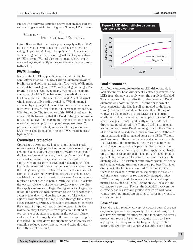
supply. The following equation shows that smaller current-sense voltages contribute to higher-efficiency LED drivers.
Figure 3 shows that choosing a power supply with a 0.25-Vreference voltage versus a supply with a 1-V referencevoltage improves efficiency. A supply with a lower current-sense voltage is more efficient regardless of input voltageor LED current. With all else being equal, a lower refer-ence voltage significantly improves efficiency and extendsbattery life.
PWM dimmingMany portable LED applications require dimming. In applications such as LCD backlighting, dimming providesbrightness and contrast adjustment. Two types of dimmingare available: analog and PWM. With analog dimming, 50%brightness is achieved by applying 50% of the maximumcurrent to the LED. Drawbacks to this method includeLED color shift and the need for an analog control signal,which is not usually readily available. PWM dimming isachieved by applying full current to the LED at a reducedduty cycle. For 50% brightness, full current is applied at a50% duty cycle. The frequency of the PWM signal must beabove 100 Hz to ensure that the PWM pulsing is not visibleto the human eye. The maximum PWM frequency dependsupon the power-supply startup and response times. Toprovide the most flexibility and ease of integration, theLED driver should be able to accept PWM frequencies ashigh as 50 kHz.
Overvoltage protectionOperating a power supply in a constant-current moderequires overvoltage protection. A constant-current supplygenerates a constant output current regardless of load. Ifthe load resistance increases, the supply’s output voltagealso must increase to supply a constant current. If thesupply encounters an excessive load resistance, or if theload is disconnected, the output voltage can increase abovethe voltage rating of the IC or of the other discrete circuitcomponents. Several overvoltage protection schemes areavailable for constant-current LED drivers. One scheme isto place a zener diode in parallel with the LEDs. This limitsthe output voltage to the zener’s breakdown voltage plusthe supply’s reference voltage. During an overvoltage con-dition, the output voltage increases to the point where thezener breaks down and begins to conduct. The output current flows through the zener, then through the current-sense resistor to ground. The supply continues to generatethe constant output current while the zener limits themaximum output voltage. A more preferred method ofovervoltage protection is to monitor the output voltageand shut down the supply when the overvoltage trip pointis reached. Shutting down the supply under an overvoltagecondition reduces power dissipation and extends batterylife in the event of a fault.
EfficiencyP
P P PLED
LED Supply Losses Current Sense=
+ +_ _
Load disconnectAn often overlooked feature in an LED-driver supply isload disconnect. Load disconnect electrically removes theLEDs from the power supply when the supply is disabled.This is important in two situations: shutdown and PWMdimming. As shown in Figure 2, during shutdown of aboost converter, the load is still connected to the inputthrough the inductor and catch diode. Since the inputvoltage is still connected to the LEDs, a small current continues to flow, even when the supply is disabled. Evensmall leakage currents significantly reduce battery lifeduring extended periods of off time. Load disconnect isalso important during PWM dimming. During the off timeof the dimming period, the supply is disabled; but the out-put capacitor is still connected across the LEDs. Withoutload disconnect, the output capacitor discharges throughthe LEDs until the dimming pulse turns the supply onagain. Since the capacitor is partially discharged at thebeginning of each dimming cycle, the supply must chargeup the output capacitor at the beginning of each dimmingcycle. This creates a spike of inrush current during eachdimming cycle. The inrush current lowers system efficiencyand creates voltage transients on the input bus. With loaddisconnect, the LEDs are removed from the circuit sothere is no leakage current when the supply is disabled,and the output capacitor remains fully charged duringPWM dimming. A load-disconnect circuit is best imple-mented by placing a MOSFET between the LEDs and thecurrent-sense resistor. Placing the MOSFET between thecurrent-sense resistor and ground creates an additionalvoltage drop that manifests itself as an error in the output-current setpoint.
Ease of useEase of use is a relative concept. A circuit’s ease of use notonly encompasses the complexity of the initial design butalso involves any future effort required to modify the circuitquickly and reuse it for other programs that may haveslightly different requirements. In general, hysteretic controllers are very easy to use. A hysteretic controller
73
75
77
79
81
83
85
Eff
icie
nc
y( %
)
2 3 4 5
V (V)IN
V = 0.25 VCS
V = 1 VCS
Figure 3. LED driver efficiency versuscurrent sense voltage

Texas Instruments IncorporatedPower Management
16
Analog Applications JournalAnalog and Mixed-Signal Products www.ti.com/sc/analogapps 1Q 2004
eliminates the need for the complicated frequency compen-sation required in a classical power-supply design. Whilefrequency compensation is not difficult for an experiencedpower-supply designer, most novice power-supply designersfind it tedious. Since the optimal compensation changesfor different input and output conditions, a classical power-supply design does not lend itself to quick modificationsfor different operating conditions. A hysteretic controlleris inherently stable and requires no changes as input andoutput conditions change.
Small sizeSmall size is an important feature for portable circuitry.Several factors contribute to the size of the circuit compo-nents. One factor is switching frequency. Higher switchingfrequencies allow the use of smaller passive components.A modern LED driver intended for portable applicationsshould be able to switch at frequencies of up to 1 MHz.Switching at frequencies greater than 1 MHz is not typi-cally recommended because it does not significantly reducecircuit size; but it does reduce efficiency and lower batterylife due to the higher switching losses. Integration of featuresinto the control IC is the single most important factor thatcontributes to a small-driver solution. If all the features
described in the preceding paragraphs were implementedwith discrete components, the board area required wouldtake up more space than the power supply itself. Integrat-ing these features into the control IC significantly reducesthe overall driver size. A second but equally importantbenefit of feature integration is a reduction in the totalsolution cost. Implemented discretely, all desirable featuresin an LED driver can add an additional sixty to seventycents in component cost. When integrated into the controlIC, these features typically add only pennies to the cost ofthe IC.
Practical solutionThe TPS61042 is an excellent example of a modern LED-driver control IC. Figure 4 is a block diagram of theTPS61042 with a highly integrated control IC. Q1 is a low-resistance, integrated power FET. The low resistance ofthis component contributes to an extremely high efficiency.The 0.25-V reference voltage reduces losses in the current-sense resistor. PWM dimming is easily implemented withthis IC by applying a PWM signal to the CTRL pin at frequen-cies as high as 50 kHz. Q2 implements the integrated load-disconnect circuitry. Since it is integrated, this circuitry isperfectly synchronized to the PWM dimming frequency.
OVP
UVLO/Bias
ControlLogic Gate Driver
V0.25 V
REF
VREF
CurrentSense
OvervoltageProtection
LED
RS
SW
VIN
Soft Start
CTRL
Enable/ControlLogic
PWMGate DriveGND
Error Comparator
VREF0.25 V
+
Q1
Q2
FB –
Figure 4. Block diagram of TPS61042 with high level of integration

Texas Instruments Incorporated Power Management
17
Analog Applications Journal 1Q 2004 www.ti.com/sc/analogapps Analog and Mixed-Signal Products
Overvoltage protection is also integrated into the IC. Mostseasoned power-supply designers will note the absence of anerror amplifier and any associated compensation circuitry.This function has been replaced by the error comparator.This IC operates with hysteretic-control feedback topology,which requires no compensation and is inherently stable.Not shown in the block diagram is the physical size of theIC. All control circuitry and features are integrated into a3 mm × 3 mm QFN package. Figure 5 shows a typicalLED-driver application that drives four LEDs with 20 mAof forward current and operates from an input voltage rangeof 1.8 to 6.0 V. The entire circuit consists of the control IC,
two small ceramic caps, an inductor, a diode, and a current-sense resistor. This small circuit shows the high level ofintegration that is achieved with today’s LED drivers. Theprimary power-supply functions and the secondary featuressuch as load disconnect, overvoltage protection, and PWMdimming have been implemented with a control IC andfive small surface-mount passive components.
Related Web sitesanalog.ti.com
www.ti.com/sc/device/TPS61042
VIN
CTRL
GND
FB
SW
OVP
LED
RS
R
13S
Ω
V
2.7 to6.0 V
IN
C
4.7 µFIN
Enable/PWM Brightness Control100 Hz to 50 kHz
C
100 nFOUT
L13.3 µH D1
Figure 5. Typical TPS61042 LED-driver solution

18
Analog Applications JournalAnalog and Mixed-Signal Products www.ti.com/sc/analogapps 1Q 2004
Estimating available application power forPower-over-Ethernet applications*
IntroductionMany existing Ethernet devices are being converted fromwall-adapter power sources to utilize the newly releasedIEEE 802.3af Power-over-Ethernet (PoE) standard. Power-system efficiency formerly was not much of an issue witha wall adapter—but PoE changes that. Applications whosefunctional circuits begin to draw power in the 10-W rangeneed close control of their power usage. This article helpsthe designer determine how much power is available whenan application operates from a PoE source.
First we will determine the net power available once thefunctions required by the 802.3af standard are performed.Then a method of modeling the usual DC/DC converters tocompute the power available for the applications circuitswill be presented, with two example topologies for compari-son. The modeling process allows the designer to identifytopology and technology issues before the first circuit isdesigned. In this discussion, application circuits are con-sidered to be everything in the powered device (PD)except the PoE front end and DC/DC converters.
PoE front-end lossesFigure 1 is a basic block diagram that shows the intercon-nection of the power-source equipment (PSE) through the
DC/DC converter and application circuits. Calculationsyielding the results in Table 1 assume that the PSE output(44 V minimum) is connected through 20 Ω of cable into aPD. The PD front end has a transformer (1 Ω total, with
Texas Instruments IncorporatedInterface
By Martin Patoka (Email: [email protected])Systems Engineer
*An edited version of this article was published December 3, 2003, onPlanetAnalog.com, an EE Times online community.
RJ-45
Data
Powered Device
1
2
3
6RX
TX
4
5
7
8
PSE44 to 57 V
PoEInterface DC/DC
0.1 µF
FunctionalCircuits
Cable
20 Ω
Figure 1. Basic PoE block diagram
PARAMETERS MIN TYP MAXPSE output (V) 44 — 57Distribution resistance (Ω) — — 20Source power (W) — — 15.4PD average current (A) — — 0.35ConstantsDiode forward drop (V) — 0.8 —Transformer resistance (Ω) — — 1PD-controller switch resistance (Ω) — 1 —PD-controller bias power (A) — 0.0012 —
Table 1. Analysis of PoE distribution and front-end losses
LOSS AVAILABLE POWERLOSS SOURCE (W) (W)15.40**
Distribution 2.45 12.95Input diode 0.56 12.39Input transformer 0.06 12.33PD-controller switch 0.12 12.21PD-controller bias 0.04 12.16
**Total PoE power available

Texas Instruments Incorporated Interface
19
Analog Applications Journal 1Q 2004 www.ti.com/sc/analogapps Analog and Mixed-Signal Products
0.5 Ω each side to the center tap), a full-wave bridge, anda hot-swap controller (or PD controller) with a 1-Ω switch(FET) in series.
There is a maximum of 12.16 W available for PD func-tional circuits. The 802.3af standard defines the 2.45-Wworst-case cable loss, and the input diode bridge dominatesthe additional front-end losses of 0.78 W.
Modeling of power-conversion stageSimple modeling techniques allow the designer to under-stand the effects of different topology and technologychoices before an actual design is done. Simple efficiencyassumptions give quick, qualitative results to allow topologycomparison and optimization. The end results will be onlyas good as the assumptions, so the designer should alwaysallow some margin by specifying the available power belowthese results.
First, let’s look at the baseline of a single-stage conver-sion to one output voltage. A single 3.3-V output converterat 90% efficiency will yield an available output power of0.9 × 12.16 = 10.9 W. Although the 90% efficiency may beviewed as optimistic, it does provide a baseline for compar-ison to other topologies.
Next we will estimate the output power available from amore complex power supply. A simple modeling techniqueis used to study how the topology and technology for eachregulator affect output power. Output voltages of +5 V at0.2 A, 3.3 V at 2 A, 2.5 V at 0.25 A, and 1.8 V at 0.25 A areassumed. These add up to a reasonable 9.6 W.
Figure 2 shows two possible supply architectures andtechnology choices. Topology 1 represents adaptation of an
existing appliance design that had a 12-V wall adapter,which was replaced with a 48-V to 12-V front end.Topology 2 attempts to maximize the available power.
To evaluate the model, start at the right-most regulators,calculating their loss and total input power, and then usethese results to evaluate the next regulator to the left. Forsimplification, assume 90% efficiency for a switcher and nobias current for linear regulators. These calculations aresummarized for the regulator types as follows.
DefinitionsIOUT = application load currentPIN_Next_Stage = power drawn by a downstream converteror linear regulator
Linear regulator stage
Switching regulator stage
P
P
OUT
IN
= ×( ) +
=
=
V I P
P
Efficiency
P P
OUT OUT IN Next Stage
OUT
Loss IN
_ _
−− POUT
POUT = ×( ) +
= ×
= −
V I P
P VP
V
P P P
OUT OUT IN Next Stage
IN INOUT
OUT
Loss IN
_ _
OOUT
48-V to 12-VSwitcher
12-V to 5-VLinear
12-V to 3.3-VSwitcher
3.3-V to 2.5-VLinear
Topology 1(Midrail Design)
2.5-V to 1.8-VLinear
5 V at0.2 A
1.8 V at0.25 A
2.5 V at0.25 A
3.3 V at2 A
Figure 2. Alternative supply topologies
48-V to 3.3-Vand 6-V
Switcher
6-V to 5-VLinear
3.3-V to 2.5-VSwitcher
2.5-V to 1.8-VLinear
Topology 2
5 V at0.2 A
1.8 V at0.25 A
2.5 V at0.25 A
3.3 V at2 A

Texas Instruments IncorporatedInterface
20
Analog Applications JournalAnalog and Mixed-Signal Products www.ti.com/sc/analogapps 1Q 2004
Using data in Table 2, let’s go through the calculationsfor the Topology 1 model shown in Figure 2. Looking atthe lower branch, Chain 1, data in Table 2, start with the1.8-V regulator’s input power and loss; notice that there isno next-stage power. The 2.5-V regulator is computed similarly, with the output power now comprised of the0.25 A to the load multiplied by 2.5 V, plus the 1.8-V regulator’s input power previously computed. The 3.3-Vswitching regulator’s input power is the total output powerdivided by the efficiency of this stage (0.9%). The powerloss of the 3.3-V regulator is still the input power minusthe output power. The upper branch is computed in a likemanner with the Chain 2 data. The 48-V to 12-V regulator’sparameters are calculated like those of the 3.3-V regulator,where the total output power is the sum of the upper- and lower-branch input powers. To get a handle on thetopology’s performance, the individual losses are summedand the apparent efficiency is computed as
The available output power in Table 2 is the input powerminus all the computed individual losses.
Topology 1’s input power exceeds the amount available.To provide a more interesting result, the 3.3-V load shownwas adjusted until the input power was 12.16 W. Bold valuesin Table 2 reflect the reduction of the 3.3-V supply loadfrom 2 A to 1.83 A.
EfficiencyTotal LossesInput Power
= −1__
.
Topology 2 is modeled with data in Table 3 much asTopology 1, with a small wrinkle. A dummy 3.3-V regulatoris modeled with an efficiency of 1 for proper totaling ofthe power and loss.
The efficiency of 90% used for the 48-V to 3.3-V converterin Topology 2 is a fairly optimistic number for a practical,synchronous output-rectifier circuit.
ConclusionAfter the 802.3af standard functions are considered, 12.16 W is the maximum power available for other electronics, including regulator losses.
The effects of topology and technology choices for PoEapplications are quite startling. Topology 1 makes only8.11 W available to the application’s circuits, while Topology 2makes 10.43 W available. This is an increase of 28%. Thebaseline single-output converter provided 10.9 W, so allthe processing represented by the additional three outputsin Topology 2 cost only 0.47 W! Using a diode output con-verter (85% efficiency) instead of a synchronous rectifierfor the 3.3-V converter drops the available power by 0.61 W.
This modeling technique allows the designer to calcu-late available output power rapidly based on topology andtechnology choices. The designer can use this informationto trade off available power, complexity, and cost.
Related Web siteanalog.ti.com
ADDITIONAL COMPUTEDOUTPUT REGULATOR INPUT REGULATOR APPLICATION OUTPUT INPUT STAGE
MODEL COMPONENTS VOLTAGE TYPE VOLTAGE EFFICIENCY CURRENT LOAD POWER LOSS(V) (V) (%) (A) (W) (W) (W)
1.8 Linear 2.5 — 0.25 0.00 0.63 0.18Chain 1 2.5 Linear 3.3 90 0.25 0.63 1.65 0.40
3.3 Switcher 12 90 1.83 1.65 8.54 0.85Chain 2 5 Linear 12 — 0.2 0.00 2.40 1.40First-stage input power — Switcher 48 90 0 10.94 12.16 1.22Total loss 4.05
Apparent efficiency = 67%Available output power = 8.11 W
Table 2. Topology 1 model
ADDITIONAL COMPUTEDOUTPUT REGULATOR INPUT REGULATOR APPLICATION OUTPUT INPUT STAGE
MODEL COMPONENTS VOLTAGE TYPE VOLTAGE EFFICIENCY CURRENT LOAD POWER LOSS(V) (V) (%) (A) (W) (W) (W)
1.8 Linear 2.5 — 0.25 0.00 0.63 0.18Chain 1 2.5 Switcher 3.3 90 0.25 0.63 1.39 0.14
3.3 — — 100 2.532 1.39 9.74 0.00Chain 2 5 Linear 6 — 0.2 0.00 1.20 0.20First-stage input power — Switcher 48 90 0 10.94 12.16 1.22Total loss 1.73
Apparent efficiency = 86%Available output power = 10.43 W
Table 3. Topology 2 model

21
Analog Applications Journal
The RS-485 unit load and maximum number of bus connections
IntroductionTIA/EIA-485 (RS-485) is apopular electrical standardfor data interchange over amultipoint differential bus.Multipoint buses are three or more stations connectedto a common transmissionmedium that allow bidirec-tional data communicationbetween any two nodes.Figure 1 schematicallyshows an example of a multi-point bus.
Maintaining a practicallimit to the output-drivecapability of an RS-485 driver requires that a limit beimposed on the steady-state load presented by the bus.This in turn constrains the input resistance of stationsand, ultimately, the maximum number of connections.
RS-485 does not specify the maximum number of busconnections. Instead, the standard defines the steady-state electrical load presented by a bus connection in unitloads. The following paragraphs explain the unit load andhow it is used to determine the maximum number ofnodes connected to an RS-485 bus segment.
The unit loadTIA/EIA-485-A defines a unit load as a 15-kΩ resistor con-nected to a –3- or 5-V source (see Figure 2). The –3-V caseapplies for positive input current, and the 5-V case appliesfor negative bus current. The definition and model arevalid for input voltages from –7 to 12 V to account for driveroutputs between 0 and 5 V, with up to ±7 V of common-mode noise voltage between a driver and receiver.
Texas Instruments Incorporated Interface
By Kevin Gingerich (Email: [email protected])High-Performance Analog/Interface Products
1Q 2004 www.ti.com/sc/analogapps Analog and Mixed-Signal Products
The number of unit loads (nUL) presented by any pro-posed connection to the RS-485 bus is then determined asthe ratio of its measured input current and the current of1 unit load. Since the current of 1 unit load is a function ofvoltage, the input current must be measured and the ratiodetermined throughout the entire –7- to 12-V input-voltagerange, with the highest ratio determining the unit-load rating.
Figure 3 shows a hypothetical example where the mea-sured input current of a circuit is nonlinear. It can beshown (see sidebar on next page) that, at its maximumvalue, the ratio of the measured and unit-load current isequal to the ratio of the slopes of the two functions andlies on a line with an intercept at –3 V for positive currentand 5 V for negative current. Conceptually, this amounts torotating a line pivoted at I = 0 mA and V = –3 V until it istangent to the curve of measured positive current versus
120 Ω 120 Ω
Figure 1. Schematic of an example multipoint bus
15 kΩI
V
+
+
–
–
–3 V for I > 05 V for I < 0
Figure 2. Electrical model of 1 unit load
0.65
–2
–1
1
2
–8 –6 –4 –2 0 2 4 6 8 10 12
Input Voltage (V)
Inp
ut
Cu
rren
t,I(m
A) I1
0
–0.78
–0.72
1.22
Figure 3. Example unit-load analysis

Texas Instruments IncorporatedInterface
22
Analog Applications JournalAnalog and Mixed-Signal Products www.ti.com/sc/analogapps 1Q 2004
voltage. For negative currents, the line is pivoted at I = 0 mAand V = 5 V. In our example, the maximum ratio occurs atmeasured input currents of 0.65 mA and –0.72 mA.
The ratio and nUL may be calculated by dividing themeasured value at the intercept by the value derived fromsolving the unit-load circuit; or, for convenience, the linesare often extended to the 12- or –7-V intercept. Since theslopes for 1 unit load and the tangential lines are constants,their ratios are constant and may be determined at anyvoltage. By definition, the current into 1 unit load at 12 Vwill be 1 mA, and at –7 V will be –0.8 mA. These valuesare respectively divided into the current-intercept valuesof the tangential lines at 12 V and –7 V, and the maximumnumber determines the nUL for the circuit. In the example,the input-current-versus-voltage characteristics of thehypothetical circuit result in 1.22 unit loads.
Maximum unit loadsThe minimum output-drive capability of a standard RS-485driver is established in clause 4.2.3 of TIA/EIA-485-A, whichspecifies a differential output voltage of at least 1.5 V witha common-mode load. Figure 4 shows a schematic of thistest circuit.
Proof that nUL is the slope ratiosLet the input current of a unit load be defined by f1 (V)and the measured circuit by f2 (V). The number of unitloads (nUL) is then
for –7 V < V < 12 V.The maximum nUL occurs when the first derivative
equals zero, or
(1)
Therefore, the maximum nUL is equal to the ratio of thefirst derivative (slopes) of the input-current function.
The following equations are used to solve for theunit-load circuit:
Substituting these into Equation 1 yields
or
These line equations mean that the input currentwhere the nUL is maximum lies on a line that intersectsthe points I = 0 mA and V = –3 V for positive currentand I = 0 mA and V = 5 V for negative current.
f V
V
ddV
f V
f Vd
dVf V V
2 2
2 2
515
115
5
( ) ( )
( ) ( ) ( ).
− =
= × −
f V
V
ddV
f V
f Vd
dVf V V
2 2
2 2
315
115
3
( ) ( )
( ) ( ) ( )
+ =
= × +
f VV
mA andd
dVf V mho1 1
515
115
( ) ( ) .= − =
f VV
mA or13
15( ) = +
f V
f V
ddV
f V
ddV
f V
2
1
2
1
( )
( )
( )
( ).=
ddV
f Vf V
f Vd
dVf V2
2
11( )
( )
( )( ).=
ddV
f V
f V f Vd
dVf V
f V
f Vd
dVf V2
1 12
2
12 1
10
( )
( ) ( )( )
( )
( )( ) .= − =
nULf V
f V= 2
1
( )
( )
375 Ω
60 ΩVOD
375 Ω
DriverUnderTest
A
B
+
+
–
–
–7 V < V < 12 VTEST
Figure 4. Differential output voltages with acommon-mode load
The 375-Ω resistors are certainly part of the common-mode load. What is not obvious is that the test voltage of–7 to 12 V actually represents a ±7-V common-mode noisesource and a 0- to 5-V local supply voltage at the load(s).This is important in that the local supply is included in theunit-load determination for this test circuit. Figure 5 showsthe common-mode test circuit with the insertion of a “local”ground used as the reference for the unit-load calculation.
To determine the unit load of this test circuit, we plotthe input-current-versus-voltage function between point Aor B and the “local” ground of Figure 5, then apply the unit-load definition described earlier. This is done in Figure 6,and we find that the current at the intercepts of the tan-gential lines is 32 mA at V = 12 V, and –32 mA at V = –7 V.By definition, this represents 32 unit loads and 40 unitloads, respectively.

Texas Instruments Incorporated Interface
23
Analog Applications Journal 1Q 2004 www.ti.com/sc/analogapps Analog and Mixed-Signal Products
The reader may have noted the discrepancy betweenthe unit-load model and the driver test circuit. One canonly assume that this was an oversight or compromise bythe authors of TIA/EIA-485. As tested, the unit-load modelshould consist of a 12-kΩ resistor to a 0- to 5-V sourcerather than 15 kΩ to a –3- to 5-V source. If we use thismodified definition, the differential output voltage withcommon-mode load test of TIA/EIA-485-A ensures that astandard driver will work with 32 unit loads.
Using the unit loadOther than a refresher on analytic geometry, of what use isthe unit-load concept to the designer of a data-interchangecircuit? Primarily, it provides a single standard parameterfor calculating the maximum number of connections andfor specifying the input characteristics of possible line circuits. Since we know a driver will support 32 unit loadsin a standard bus configuration, we need only divide 32 bythe total number of nodes (N) to derive the maximum
UNIT MAXIMUM NUMBER OF DEVICES PARTLOADS ON A SINGLE BUS SEGMENT NUMBER
SN65HVD05SN65HVD10
0.5 64 SN65HVD20SN65HVD23SN65LBC182
0.25 128 SN65LBC184SN65HVD06SN65HVD07SN65HVD08SN65HVD11
0.125 256 SN65HVD12SN65HVD21SN65HVD22SN65HVD24
Table 1. Fractional unit-load devices from TI
375 Ω
375 Ω
A
B
+
+
–
–
0 to 5 V
Local Ground
–7 V < V < 7 VNOISE
Figure 5. Physical representation of thetest circuit
unit-load rating for each of the line circuits. For example,if 48 nodes were to be connected, each line receiver ortransceiver would have to have no more than 0.67 unitloads (32/48).
The unit load also can be useful when nonstandard busconfigurations are implemented. In addition to the differen-tial termination of the differential signal pair, pull-up andpull-down resistors often are connected to the lines to pro-vide a known bus state when all of the connected driversare idle. The resistor values used for this fail-safe termina-tion are usually around 1 kΩ. If so, this termination wouldconsume 12 unit loads (12 mA at 12 V) out of the budget of32 unit loads. This leaves 20 unit loads for the line circuits;and, if 48 nodes are still to be connected, each of the linecircuits must now be no more than 0.42 unit loads (20/48).
Texas Instruments (TI) offers numerous options, someof which are shown in Table 1, for supporting a large number of RS-485 bus connections.
–40
–30
–20
–10
0
10
20
30
40
–10 –5 0 5 10 15
Input Voltage (V)
Inp
ut
Cu
rren
t,I
(mA
)
32 mA/1 mA = 32 Unit Loads
–32 mA/ –0.8 mA = 40 Unit Loads
–3
–7
12
Figure 6. Unit load of common-mode test circuit
ConclusionThe unit load is a relative parameter that provides a basisfor determining the maximum number of connections to anRS-485 bus segment or for specifying the input character-istics of line circuits. A standard RS-485 driver will handle32 unit loads that could consist of 256 devices with a ratingof 1/8 unit load.
Related Web sitesanalog.ti.com
www.ti.com/sc/device/partnumber
Replace partnumber with SN65HVD05, SN65HVD06,SN65HVD07, SN65HVD08, SN65HVD10, SN65HVD11,SN65HVD12, SN65HVD20, SN65HVD21, SN65HVD22,SN65HVD23, SN65HVD24, SN65LBC182 or SN65LBC184

24
Analog Applications JournalAnalog and Mixed-Signal Products www.ti.com/sc/analogapps 1Q 2004
Op amp stability and input capacitance
IntroductionOp amp instability is compensated out with the addition ofan external RC network to the circuit. There are thousandsof different op amps, but all of them fall into two categories:uncompensated and internally compensated. Uncompen-sated op amps always require external compensation components to achieve stability; while internally compen-sated op amps are stable, under limited conditions, withno additional external components.
Internally compensated op amps can be made unstablein several ways: by driving capacitive loads, by addingcapacitance to the inverting input lead, and by adding inphase feedback with external components. Adding in phasefeedback is a popular method of making an oscillator thatis beyond the scope of this article. Input capacitance ishard to avoid because the op amp leads have stray capaci-tance and the printed circuit board contributes some straycapacitance, so many internally compensated op amp circuits require external compensation to restore stability.Output capacitance comes in the form of some kind ofload—a cable, converter-input capacitance, or filter capacitance—and reduces stability in buffer configurations.
Stability theory reviewThe theory for the op amp circuit shown in Figure 1 istaken from Reference 1, Chapter 6. The loop gain, Aβ, iscritical because it solely determines stability; input circuitsand sources have no effect on stability because inputs aregrounded for the stability analysis. Equation 1 is the loop-gain equation for the resistive case where Z = R.
(1)
Beware of Equation 1; its simplicity fools peoplebecause they make the assumption that A = a, which isnot true for all cases. Stability can be determined easilyfrom a plot of the loop gain versus frequency. The criticalpoint is when the loop gain equals 0 dB (gain equals 1)because a circuit must have a gain ≥1 to become unstable.The phase margin, which is the difference between themeasured phase angle and 180º, is calculated at the 0-dBpoint. A typical open-loop-gain curve for the TLV278xfamily of op amps is used as a teaching example and isshown in Figure 2.
The op amp’s open-loop gain and phase (a in Equation 1)are represented in Figure 2 by the left and right verticalaxes, respectively. Never assume that the op amp open-loop-gain curve is identical to the loop gain because externalcomponents have to be accounted for to get the loop-gain
AaR
R RG
F Gβ = +
curve. When RF = 0 and RG = ∞, the op amp reduces to anoninverting buffer amp (unity gain) and the loop gainbecomes equal to the op amp open-loop gain. We canobtain the buffer phase margin directly from Figure 2 bytracing the gain line down from its vertical intercept (atapproximately 78 dB) to where it crosses the 0-dB line atapproximately 8 MHz. Then we can trace the 8-MHz lineup until it intersects the phase curve, and read the phasemargin as approximately 56º. This plot was made withphase margin, but many plots are made instead with phaseshift. For plots made with phase shift, the phase shift mustbe subtracted from 180º to obtain the phase margin.
Now that we have the phase margin, what can we dowith it other than to say that the circuit does not oscillate?
Texas Instruments IncorporatedAmplifiers: Op Amps
By Ron Mancini (Email: [email protected])Staff Scientist, Advanced Analog Products
VIN2
VIN1
VOUT+
–
ZG ZF
ZG
ZF
Figure 1. Equation 1 can be written from the opamp schematic by opening the feedback loopand calculating gain
240
210
180
150
120
90
60
30
0
–30
–60
–90
–120
Ph
ase M
arg
in (
deg
rees)
0
20
40
70
80
1 k 10 k 100 k
Frequency, f (Hz)
Dif
fere
nti
al V
olt
ag
e A
mp
lifi
cati
on
, A
VD
(d
B)
60
50
30
10
–10
–20
–30
–401 M 10 M
VDD = 1.8 V & 2.7 V
RL= 2 kΩCL = 10 pF
TA = 25˚C
Gain
Phase
Figure 2. Open-loop-gain/phase curves arecritical stability-analysis tools

Texas Instruments Incorporated Amplifiers: Op Amps
25
Analog Applications Journal 1Q 2004 www.ti.com/sc/analogapps Analog and Mixed-Signal Products
Figure 3 is a plot of phase margin and percent maximumovershoot versus a dummy variable, the damping ratio.Enter this plot at a phase margin of 56º and go up to thephase curve intersection. At this point, go horizontally(constant damping ratio) to the intersection of the over-shoot curve, and then drop down to read an overshoot ofapproximately 11%. This plot enables the designer to pre-dict the transient step response from the phase margin,and transient response is a measure of relative stability.
0.4
0.2
00 10 20 30 40 50 60
Da
mp
ing
Ra
tio
0.6
0.8
1
70 80
Phase Margin
Percent Maximum
Overshoot
Phase Margin, φM (degrees)
Maximum Overshoot (%)
Figure 3. Phase margin/percent overshootversus damping ratio
VIN2
VIN1
VOUT
CCM
+
–
RG RF
RG
CCM
CID
RF
Figure 4. Input capacitance includes ICinternal, lead, and PCB capacitance
0.110
Frequency, f (Hz)
100 k
10 k
1 k
100
10
1
100 1 k 10 k 100 k 1 M 10 M
0
30
60
90
120
150
180
Ph
ase
Sh
ift
(de
gre
es)
VCC± = ±15 V
RL = 10 kΩCL = 25 pF
TA = 25˚C
Phase Shift
La
rge
-Sig
na
l D
iffe
ren
tia
l
Vo
lta
ge
Am
pli
fica
tio
n, A
VD
(V
/mV
)
AVD
Figure 5. Gain/phase plots of medium-frequencyop amps show frequency extremes
The external resistors come into play when the op ampis conFigured as an inverting, noninverting, or differentialamplifier. When RF = RG, Equation 1 reduces to Aβ = a/2;and the vertical intercept for the amplifier reduces fromthat of the buffer by 6 dB. Although the vertical intercepthas changed, the pole location remains constant becausegain is not tied to phase. The 0-dB crossover frequencychanges to approximately 3 MHz because of the gain drop;the phase margin increases to approximately 87º; and thepercent overshoot is negligible. Notice that the buffer isless stable than any of the amplifier circuits and that, atthe same phase margin, the inverting gain is –1 while thenoninverting gain is 2.
Added input capacitance and its effectWhen input capacitors are added to the circuit (see Figure 4), they cause a pole to occur in the loop gain, asshown in Equation 2.
(2)
The input capacitor, CIN, is the summation of all theinverting input capacitances, and it adds a pole to the loop
AaZ
Z R
aR
R R R R CG
G F
G
G F G F IN
β = + = + ×+
1
1
gain. Adding a pole to the loop gain does not always changethe stability because the pole location and its added phaseshift may not affect the phase margin. Consider the casewhere the pole is located at a very high frequency—say,100 MHz—for the TLV278x. Notice from Figure 2 that theop amp open-loop gain is so low above 10 MHz that theoverall gain can never equal 1, so the added pole is of novalue. The case where the pole is located at a very low frequency—say, 0.001 Hz—is harder to calculate becausethe low-frequency response is not shown in Figure 2.However, we can be sure that the phase shift is close to zeroat this frequency. A pole with a frequency intercept thatlow would cause the gain to be down 120 dB at 1 kHz, andagain the loop gain would be less than 1 before the phasemargin went to zero. An op amp open-loop gain/phase plotthat shows low-frequency response is shown in Figure 5.Notice that the phase shift (not phase margin in this plot)approaches zero at low frequencies. In addition, notice thatthe phase shift approaches 180º at very high frequenciesand that the gain is given in ratios rather than in decibels.

Texas Instruments IncorporatedAmplifiers: Op Amps
26
Analog Applications JournalAnalog and Mixed-Signal Products www.ti.com/sc/analogapps 1Q 2004
The DC gain in Equation 2 remains the same as it waswithout an input capacitor, but the pole is added at f = 1/(2πRF||RGCIN). If this pole occurs at approximately 3 MHz, it reduces the gain by 3 dB and adds a 45º phase shiftat that frequency. Using CIN = 20 pF and RG||RF = 2.7 kΩyields a 3-dB frequency of 2.94 MHz, so it is reasonable toassume a pole frequency of 3 MHz. The gain in Figure 4must be moved down 9 dB to account for the resistors andthe pole. The new 0-dB crossover frequency is 2 MHz, andthe phase margin at 2 MHz (as shown in Figure 4) is 89º.The pole phase shift of 45º must be subtracted from thecurve phase margin to obtain the final circuit phase margin;thus φ = 89º – 45º = 44º. The percent overshoot correspond-ing to the 44º phase margin is 24.45%. Adding CIN reducesthe phase margin from 87º in the purely resistive case to44º with input capacitance. If the op amp initially had lessthan a 44º phase margin, the circuit would be unstablerather than just bouncy.
If the resistor values were larger than 5.4 kΩ, the polewould move down in frequency. The exact pole locationthat does the most damage to stability is hard to calculatebecause the phase is a nonlinear tangent function. In thiscase, it is best to move the resistors down in value toabout 1 kΩ, thus moving the pole to 8 MHz and reducingthe added phase shift to about 14º. A second problemcrops up in the noninverting configuration because CIDcouples a portion of the input signal to the inverting input.This action reduces the common-mode rejection capabilityand introduces high-frequency distortion.
The buffer circuit with an input capacitance is shown inFigure 6. Notice that the input capacitance includes theoutput capacitance and load capacitance in the absence ofa feedback resistor, and that the output impedance, ZOUT,comes into play.
The buffer loop gain is given as
(3)
First, consider the case when RF = 0; ZOUT is obtainedfrom Figure 7 as 70 Ω at 8 MHz. Assuming that the input,output, and load capacitance is 100 pF, the pole frequencyis located at 22.7 MHz; and this pole adds a 19.4º phaseshift at the 0-dB crossover frequency. This added phaseshift subtracts directly from the previously calculatedphase margin of 56º because the pole attenuation doesn’t
Aa
R Z CF OUT IN
β =+( ) +1
.
VIN
VOUT
+
RF
ZOUT
a
CIN
Figure 6. Input, output, and load capacitorsare in parallel in the buffer circuit
Frequency, f (Hz)
100 1 k 10 k 100 k 1 M 10 M
Ou
tpu
t Im
ped
an
ce, Z
O (
Ω)
0.1
10
1
100
AV = 10
AV = 1
VDD = 2.7 V
TA = 25˚C
Figure 7. Op amp output impedance increaseswith increasing frequency

Texas Instruments Incorporated Amplifiers: Op Amps
27
Analog Applications Journal 1Q 2004 www.ti.com/sc/analogapps Analog and Mixed-Signal Products
occur until after the 0-dB crossover frequency. This circuithas a phase margin of 56º – 19.4º = 36.6º, leading to anovershoot of 33%.
When RF = 1 kΩ, the RFCIN pole is located at 8 MHz; so it becomes dominant. Under these conditions, the gaincurve moves down 3 dB and the phase shift is increased45º. Moving the gain curve down 3 dB yields an 80º phasemargin at f = 4 MHz. Subtracting 45º plus 19.4º from 80ºyields a phase margin of 15.6º, and the overshoot increasesto approximately 50%. It is obvious that increasing thevalue of RF makes it dominant over ZOUT and will quicklymake the circuit oscillate.
CF increases stabilityInput and output capacitors always decrease stability. Inputcapacitors are a pole in the open-loop transfer function,but they are a zero in the closed-loop transfer function.The closed-loop zero increases the circuit (not the opamp) bandwidth, so sometimes input capacitors are addedto the circuit to improve high-frequency response.
A capacitor placed in parallel with the feedback resistor,CF, introduces a zero into the loop gain:
(4)
When the closed-loop gain is greater than 1 and CF isgreater than CG, the zero precedes the pole. In this case,which is not unusual, the zero contributes a positive phaseshift to the loop-gain plot, causing an increase in stability.The more the zero leads the pole, the more stable the
AaR
R R
R C
R R C CG
F G
F F
F G F G
β = + ×+
+( ) +
1
1
circuit becomes; but the pole always ends up cancelingthe zero. The idea is to place the zero so that we achievethe required overshoot and then to accept the pole loca-tion. The open-loop zero translates to a closed-loop pole;thus CF always decreases high-frequency performance.Optimal performance is gained when the acceptable over-shoot is obtained at an acceptable frequency response.
ConclusionThe addition of input, output, or load capacitance to an opamp circuit decreases stability, which leads to overshoot inthe time domain. The stability decrease is worse for abuffer than for other amplifier configurations. Reducingthe resistance value that makes up the RC circuit reducesthe effect of the capacitance; this effect leads to the ruleof thumb that high frequencies and low resistance gotogether. Input capacitance is easily compensated byadding a feedback capacitor into the circuit. The value ofthe feedback capacitor should be just large enough toachieve the desired overshoot response, because largervalues cause a loss of high-frequency performance.
Reference1. Ron Mancini, Op Amps For Everyone (Newnes
Publishers, 2003). An earlier 2002 edition is available atwww-s.ti.com/sc/techlit/slod006
Related Web sitesanalog.ti.com
www.ti.com/sc/device/TLV278x

28
Analog Applications JournalAnalog and Mixed-Signal Products www.ti.com/sc/analogapps 1Q 2004
Integrated logarithmic amplifiers for industrial applications
Many industrial applications measure physical quantitiesover a wide dynamic range. These applications use loga-rithmic amplifiers (log amps) to match a transmitter’sdynamic output to the linear input range of a signal gauge.Figure 1 shows a typical signal chain to measure photocurrents over a dynamic range of seven decades.
Log amps of the past were built with hybrid techniques.Today’s CMOS technology enables the integration of the log-ging circuit and additional support functions, such as voltagereferences and uncommitted op amps, into a single chip.
This article describes the operation and architecture ofintegrated log amps and provides two application examplesusing the Texas Instruments (TI) LOG112 and LOG2112.
For a forward-biased diode, the forward current is largerby far than the reverse current (IF >> IS). Thus, Equation 2simplifies to
(3)
A simple log amp whose transfer function satisfiesEquation 3 is shown in Figure 3. The op amp operates asan inverting amplifier with a feedback diode. With thediode being virtually anode-grounded, the op amp needsto generate a negative output voltage to forward bias thediode. For a given input current, IIN, the correspondingoutput voltage, VOUT, is
(4)V m VI
IOUT TIN
S= − × × ln .
V m VI
IF TF
S= × × ln .
Texas Instruments IncorporatedAmplifiers: Op Amps
By Thomas Kugelstadt (Email: [email protected])Senior Systems Engineer, Industrial Systems
100 pA to 1 mA(7 decades)
0 to 5 V(1 decade)
PhotoDetector
Log Amp Voltmeter
Figure 1. Matching a sensor’s dynamic outputto the linear input of a voltmeter
VF
VFIF
IF
y
x
y
x
Figure 2. Diode characteristic in exponentialand logarithmic form
IIN
+
I IIN = F
VF
V = –VOUT F
–
Figure 3. Log amp with diode
OperationA log amp makes use of the logarithmic relationshipbetween the voltage and current of a forward-biaseddiode. Figure 2 shows the characteristic of the forwardcurrent, given by the exponential function
(1)
where VF and IF are the forward voltage and forward current of the diode, respectively; IS is the theoreticalreverse-saturation current; m is a correction factor; and VTis the temperature-equivalent voltage. Exchanging the xfor the y axes and vice versa yields the forward voltage asa logarithmic function of the forward current. Mathemat-ically, this corresponds to solving Equation 1 for VF:
(2)V m VI
IF TF
S= × × −
ln .1
I I eF S T
V
m VF
T= × −
×( ) ,1

Texas Instruments Incorporated Amplifiers: Op Amps
29
Analog Applications Journal 1Q 2004 www.ti.com/sc/analogapps Analog and Mixed-Signal Products
The drawback of this circuit is that VOUT depends not onlyon IIN but also on m, IS(T), and VT, all of which are eithercurrent- or temperature-dependent.
• The correction factor, m, takes into account the devia-tion between the diode characteristic and Shockley’ssimplified theory of diodes. However, m strongly dependson the forward current, thus varying its value between 1 and 2.
• The reverse-saturation current, IS, is temperature-dependent. For a constant forward current, IS doubleswith every 10-K increase in temperature. Thus, for a100-K rise in temperature, IS increases by a factor of 1000.
• The temperature-equivalent voltage, VT = k × T/e0,increases linearly with temperature. With Boltzman’sconstant k = 1.38 × 10⁻²³ J/K, the electron charge e0 = 1.6 × 10⁻¹⁹ C, and an ambient temperature of T = 296 K (23ºC), VT yields
When the circuit operates at a constant temperature, theimpact of m still limits the measurable input range to 1 or 2decades of acceptable accuracy. To eliminate m, the diodeis replaced by a transistor (Figure 4). Its exponentialtransfer characteristic in Figure 5 is similar to that of adiode. In contrast to a diode, however, the correction factor equals 1 and simplifies Equation 4 to
(5)
The input current, IIN, becomes the collector current, IC;and IS becomes the emitter reverse-saturation current, IES.The elimination of m increases the measurable input rangeto several decades. VOUT, however, is still temperature-dependent via IES(T) and VT. Therefore, it is impossible todetermine whether a change in VOUT is caused by theinput current or by a change in temperature.
V VI
Ior V V
I
IOUT TC
ESBE T
C
ES= − × = ×ln , ln .
VJ K K
CmVT = × ×
×=
−
−1 38 10 296
1 6 1025 5
23
19
. /.
. .
To avoid output changes due to temperature, the temperature-compensated log amp in Figure 6 is required.Here, generating the difference of two logarithms eliminatesIES. From the previous example, we take the logarithmicrelationship between the basis-emitter voltage, VBE, andthe collector current, IC, for both transistors, Q1 and Q2:
V VI
Iand V V
I
IBE TC
ESBE T
C
ES1
1
12
2
2= × = ×ln , ln .
IIN
+
V = VF BE
V = –VOUT BE
–
Figure 4. Log amp with transistor
IC
VBE
VCE
Figure 5. Transistor input characteristic
Q2 Q1
R1
R2(T)
VOUT
V1(T)
I = IIN2 C2
I = IIN1 C1
+
–
+
–A2
A1
Figure 6. Temperature-compensated log amp

Texas Instruments IncorporatedAmplifiers: Op Amps
30
Analog Applications JournalAnalog and Mixed-Signal Products www.ti.com/sc/analogapps 1Q 2004
The two logging transistors build a difference amplifierwhose output voltage, V1, yields the difference of bothbase-emitter voltages:
(6)
With matched and isothermal transistors, IES1 = IES2 = IS,and Equation 6 simplifies to
(7)
A remaining temperature dependency exists via only VT.Via the voltage divider, R1 and R2, V1 represents only apart of the entire circuit’s output voltage, VOUT:
(8)
To compensate for the effect of VT, R2 is replaced by atemperature-dependent resistor with a positive tempera-ture coefficient. This keeps
constant over a certain temperature range. Practical valuesfor the temperature coefficient vary between 3500 and3700 ppm/K.
During the manufacturing process of log amps, theinternal components and the temperature coefficient aretrimmed to a fixed value. In addition, the natural loga-rithm is converted to log10 by applying a correction factor,n = 2.3, according to ln x = 2.3 × log x. The expression (1 + R1/R2(T)) × VT × 2.3 becomes a constant, q, with theunit V/decade, simplifying the computation of VOUT to
(9)V qI
IOUTC
C= × log .1
2
1 1
2+
×
R
RV
TT
( )
VR
RV
R
RV
I
IOUT T TC
C( ) ln .= +
× = +
× ×1 11
21
1
2
1
2
V VI
IT TC
C1
1
2( ) ln .= ×
V V V VI
IV
I
IBE BE TC
EST
C
ES1 1 2
1
1
2
2= − = × − ×ln ln .
Log-amp structureFigure 7 shows a block diagram of the integrated log amp,LOG112. The actual logging circuit consists of the ampli-fiers, A1 and A2, and the transistors, Q1 and Q2. The designation of the collector currents, IC1 and IC2, changesto I1 and I2. In most cases, I1 represents the input currentto be measured, while I2 is the reference current for thelogarithmic computation.
The device minimizes external component count by providing a voltage reference and an uncommitted opamp, A3, on-chip. The reference allows I2 to be generatedvia an external resistor, RREF. Via A3, the logarithmic out-put signal, VLOGOUT, can be filtered or further amplified. A3also can be configured as a comparator to provide a loss-of-signal indication.
The LOG112 is trimmed to provide an output voltage of0.5 V per decade of input current. The device uses patentedtemperature compensation in which R2 is laid out as an alu-minum frame with a temperature coefficient of 3700 ppm/K,resulting in extremely temperature-stable operation. Foran input current of 10 µA, for example, the output voltagechanges by only 50 µV/K.
The output voltage of the log amp is made available atthe VLOGOUT pin:
with input currents ranging from 100 pA to 3.5 mA. Thevoltage at the VOUT3 pin is defined via the external gain, G = 1 + RF/RG, and yields
V G V GI
IOUT LOGOUT31
20 5= × = × ×. log .
VI
ILOGOUT = ×0 5 1
2. log ,
A2
A1
Q1 Q2
CC
I1
VOUT3
LOG112
A3
RFR
R
R
G
1
2(T)
RREF
VLOGOUT
–V+V
I2
REF
Figure 7. Internal block diagram of LOG112

Texas Instruments Incorporated Amplifiers: Op Amps
31
Analog Applications Journal 1Q 2004 www.ti.com/sc/analogapps Analog and Mixed-Signal Products
Application examplesThe circuit in Figure 8 controls the opti-cal output power of a laser diode (LD1).With the output power decreasing overthe lifetime of the diode, a control loopthat keeps the output power constant isrequired. In the feedback path, a fractionof the output signal is fed back via aphotodiode (PD1) and converted intoelectrical current.
The laser is calibrated by making thereference current, IREF, equal to the PD1current, I1. Deviations between IREF andI1 are converted into an error signal andapplied to the bias input of the laser-diode driver. The driver then changesthe bias current of LD1 until the errorsignal diminishes to zero.
Another application example is theconstant-gain control and gain adjust-ment of an op amp shown in Figure 9.Two log amps measure the optical input and output powerof the amplifier. A difference amplifier subtracts the outputsignals of both log amps and applies an error voltage tothe proportional-integral-derivative (PID) controller. The
LOG112
LOG
I1
Laser Module
Fiber
PD1 LD1A3
REF
IREF
Laser-DiodeDriver
ILASER
VERROR
Figure 8. Controlling the optical output power of a laser diode
IL
PID
Diff
LOG2LOG1
REF
DAC
LOG2112
Tap Tap
I1
IREF1 IREF2
I2
RREF2RREF1
VCCS
Pump Laser
Fiber
VERROR
VOUT1 VOUT2
1% 1%
Figure 9. Constant-gain control and gain adjustment of an op amp
controller output adjusts a voltage-controlled currentsource (VCCS), which then drives the actual pump laser.The amplifier operates at the desired optical gain whenthe error voltage at the PID output is zero.

Texas Instruments IncorporatedAmplifiers: Op Amps
32
Analog Applications JournalAnalog and Mixed-Signal Products www.ti.com/sc/analogapps 1Q 2004
The preceding equation shows that the optical gain of theamplifier is adjusted simply by reducing IREF1 by a factorof GOPT smaller than IREF2. In addition to the constant-gaincontrol, this circuit also allows the electronic gain settingof GOPT in the range of 0 to 30 dB.
LOG2112 is well suited for this application. The devicecontains two log amps to measure the input and outputpower; an on-chip voltage reference to generate IREF2; andtwo uncommitted op amps configurable as differenceamplifier and PID controller.
ConclusionTI offers a series of integrated, high-precision log ampswith varying input-current ranges and output-scale factors.
Related Web sitesanalog.ti.com
www.ti.com/sc/device/LOG112
The log amp at the amplifier input builds the referencesource. Its output voltage is
where I1 is the input photo current and IREF1 is an adjust-able reference current. The log amp at the amplifier outputprovides an output voltage of
where I2 is the output photo current and IREF2 is a fixedreference current.
It is important to observe that I2 = I1 × GOPT, whereGOPT is the optical gain factor. In steady state, the outputvoltages of both log amps are equal (V1 = V2), and
Solving for GOPT yields
GI
IOPTREF
REF= 2
1.
log log , .I
I
I G
Ior
I
I
I G
IREF
OPT
REF REF
OPT
REF
1
1
1
2
1
1
1
2=
×=
×
VI
IOUTREF
22
2= log ,
VI
IOUTREF
11
1= log ,

33
Analog Applications Journal
Texas Instruments Incorporated Index of Articles
1Q 2004 www.ti.com/sc/analogapps Analog and Mixed-Signal Products
Title Issue Page
Data AcquisitionAspects of data acquisition system design . . . . . . . . . . . . . . . . . . . . . . . . . . . . . . . . . . . . . . . . . . .August 1999 . . . . . . . . . . . .1Low-power data acquisition sub-system using the TI TLV1572 . . . . . . . . . . . . . . . . . . . . . . . . . .August 1999 . . . . . . . . . . . .4Evaluating operational amplifiers as input amplifiers for A-to-D converters . . . . . . . . . . . . . . . .August 1999 . . . . . . . . . . . .7Precision voltage references . . . . . . . . . . . . . . . . . . . . . . . . . . . . . . . . . . . . . . . . . . . . . . . . . . . . . . .November 1999 . . . . . . . . .1Techniques for sampling high-speed graphics with lower-speed A/D converters . . . . . . . . . . . .November 1999 . . . . . . . . .5A methodology of interfacing serial A-to-D converters to DSPs . . . . . . . . . . . . . . . . . . . . . . . . . .February 2000 . . . . . . . . . .1The operation of the SAR-ADC based on charge redistribution . . . . . . . . . . . . . . . . . . . . . . . . . .February 2000 . . . . . . . . .10The design and performance of a precision voltage reference circuit for 14-bit and
16-bit A-to-D and D-to-A converters . . . . . . . . . . . . . . . . . . . . . . . . . . . . . . . . . . . . . . . . . . . . . .May 2000 . . . . . . . . . . . . . .1Introduction to phase-locked loop system modeling . . . . . . . . . . . . . . . . . . . . . . . . . . . . . . . . . . .May 2000 . . . . . . . . . . . . . .5New DSP development environment includes data converter plug-ins (PDF - 86 Kb) . . . . . . .August 2000 . . . . . . . . . . . .1Higher data throughput for DSP analog-to-digital converters (PDF - 94 Kb) . . . . . . . . . . . . . . .August 2000 . . . . . . . . . . . .5Efficiently interfacing serial data converters to high-speed DSPs (PDF - 80 Kb) . . . . . . . . . . . .August 2000 . . . . . . . . . . .10Smallest DSP-compatible ADC provides simplest DSP interface (PDF - 120 Kb) . . . . . . . . . . . .November 2000 . . . . . . . . .1Hardware auto-identification and software auto-configuration for the
TLV320AIC10 DSP Codec — a “plug-and-play” algorithm (PDF - 105 Kb) . . . . . . . . . . . . . .November 2000 . . . . . . . . .8Using quad and octal ADCs in SPI mode (PDF - 94 Kb) . . . . . . . . . . . . . . . . . . . . . . . . . . . . . . . .November 2000 . . . . . . . .15Building a simple data acquisition system using the TMS320C31 DSP (PDF - 235 Kb) . . . . . .February 2001 . . . . . . . . . .1Using SPI synchronous communication with data converters — interfacing the
MSP430F149 and TLV5616 (PDF - 182 Kb) . . . . . . . . . . . . . . . . . . . . . . . . . . . . . . . . . . . . . . .February 2001 . . . . . . . . . .7A/D and D/A conversion of PC graphics and component video signals, Part 1: Hardware
(PDF - 191 Kb) . . . . . . . . . . . . . . . . . . . . . . . . . . . . . . . . . . . . . . . . . . . . . . . . . . . . . . . . . . . . . .February 2001 . . . . . . . . .11A/D and D/A conversion of PC graphics and component video signals, Part 2: Software
and control . . . . . . . . . . . . . . . . . . . . . . . . . . . . . . . . . . . . . . . . . . . . . . . . . . . . . . . . . . . . . . . . . .July 2001 . . . . . . . . . . . . . .5Intelligent sensor system maximizes battery life: Interfacing the MSP430F123
Flash MCU, ADS7822, and TPS60311 . . . . . . . . . . . . . . . . . . . . . . . . . . . . . . . . . . . . . . . . . . . . .First Quarter, 2002 . . . . . .5SHDSL AFE1230 application . . . . . . . . . . . . . . . . . . . . . . . . . . . . . . . . . . . . . . . . . . . . . . . . . . . . . .Second Quarter, 2002 . . . .5Synchronizing non-FIFO variations of the THS1206 . . . . . . . . . . . . . . . . . . . . . . . . . . . . . . . . . . .Second Quarter, 2002 . . .12Adjusting the A/D voltage reference to provide gain . . . . . . . . . . . . . . . . . . . . . . . . . . . . . . . . . . .Third Quarter, 2002 . . . . .5MSC1210 debugging strategies for high-precision smart sensors . . . . . . . . . . . . . . . . . . . . . . . . .Third Quarter, 2002 . . . . .7Using direct data transfer to maximize data acquisition throughput . . . . . . . . . . . . . . . . . . . . . .Third Quarter, 2002 . . . .14Interfacing op amps and analog-to-digital converters . . . . . . . . . . . . . . . . . . . . . . . . . . . . . . . . . .Fourth Quarter, 2002 . . . .5ADS82x ADC with non-uniform sampling clock . . . . . . . . . . . . . . . . . . . . . . . . . . . . . . . . . . . . . . .Fourth Quarter, 2003 . . . .5Calculating noise figure and third-order intercept in ADCs . . . . . . . . . . . . . . . . . . . . . . . . . . . . .Fourth Quarter, 2003 . . .11Evaluation criteria for ADSL analog front end . . . . . . . . . . . . . . . . . . . . . . . . . . . . . . . . . . . . . . . .Fourth Quarter, 2003 . . .16Two-channel, 500-kSPS operation of the ADS8361 . . . . . . . . . . . . . . . . . . . . . . . . . . . . . . . . . . . .First Quarter, 2004 . . . . . .5ADS809 analog-to-digital converter with large input pulse signal . . . . . . . . . . . . . . . . . . . . . . . . .First Quarter, 2004 . . . . . .8
Power ManagementStability analysis of low-dropout linear regulators with a PMOS pass element . . . . . . . . . . . . . .August 1999 . . . . . . . . . . .10Extended output voltage adjustment (0 V to 3.5 V) using the TI TPS5210 . . . . . . . . . . . . . . . .August 1999 . . . . . . . . . . .13Migrating from the TI TL770x to the TI TLC770x . . . . . . . . . . . . . . . . . . . . . . . . . . . . . . . . . . . . .August 1999 . . . . . . . . . . .14TI TPS5602 for powering TI’s DSP . . . . . . . . . . . . . . . . . . . . . . . . . . . . . . . . . . . . . . . . . . . . . . . . . .November 1999 . . . . . . . . .8Synchronous buck regulator design using the TI TPS5211 high-frequency
hysteretic controller . . . . . . . . . . . . . . . . . . . . . . . . . . . . . . . . . . . . . . . . . . . . . . . . . . . . . . . . . . .November 1999 . . . . . . . .10Understanding the stable range of equivalent series resistance of an LDO regulator . . . . . . . . .November 1999 . . . . . . . .14Power supply solutions for TI DSPs using synchronous buck converters . . . . . . . . . . . . . . . . . .February 2000 . . . . . . . . .12Powering Celeron-type microprocessors using TI’s TPS5210 and TPS5211 controllers . . . . . . .February 2000 . . . . . . . . .20
Index of Articles

Texas Instruments IncorporatedIndex of Articles
34
Analog Applications JournalAnalog and Mixed-Signal Products www.ti.com/sc/analogapps 1Q 2004
Title Issue Page
Power Management (Continued)Simple design of an ultra-low-ripple DC/DC boost converter with TPS60100 charge pump . . .May 2000 . . . . . . . . . . . . .11Low-cost, minimum-size solution for powering future-generation CeleronTM-type
processors with peak currents up to 26 A . . . . . . . . . . . . . . . . . . . . . . . . . . . . . . . . . . . . . . . . .May 2000 . . . . . . . . . . . . .14Advantages of using PMOS-type low-dropout linear regulators in battery applications
(PDF - 216 Kb) . . . . . . . . . . . . . . . . . . . . . . . . . . . . . . . . . . . . . . . . . . . . . . . . . . . . . . . . . . . . . . .August 2000 . . . . . . . . . . .16Optimal output filter design for microprocessor or DSP power supply (PDF - 748 Kb) . . . . . .August 2000 . . . . . . . . . . .22Understanding the load-transient response of LDOs (PDF - 241 Kb) . . . . . . . . . . . . . . . . . . . . .November 2000 . . . . . . . .19Comparison of different power supplies for portable DSP solutions
working from a single-cell battery (PDF - 136 Kb) . . . . . . . . . . . . . . . . . . . . . . . . . . . . . . . . . .November 2000 . . . . . . . .24Optimal design for an interleaved synchronous buck converter under high-slew-rate,
load-current transient conditions (PDF - 206 Kb) . . . . . . . . . . . . . . . . . . . . . . . . . . . . . . . . . .February 2001 . . . . . . . . .15–48-V/+48-V hot-swap applications (PDF - 189 Kb) . . . . . . . . . . . . . . . . . . . . . . . . . . . . . . . . . . .February 2001 . . . . . . . . .20Power supply solution for DDR bus termination . . . . . . . . . . . . . . . . . . . . . . . . . . . . . . . . . . . . . .July 2001 . . . . . . . . . . . . . .9Runtime power control for DSPs using the TPS62000 buck converter . . . . . . . . . . . . . . . . . . . .July 2001 . . . . . . . . . . . . .15Power control design key to realizing InfiniBandSM benefits . . . . . . . . . . . . . . . . . . . . . . . . . . . . .First Quarter, 2002 . . . . .10Comparing magnetic and piezoelectric transformer approaches in CCFL applications . . . . . . .First Quarter, 2002 . . . . .12Why use a wall adapter for ac input power? . . . . . . . . . . . . . . . . . . . . . . . . . . . . . . . . . . . . . . . . . .First Quarter, 2002 . . . . .18SWIFTTM Designer power supply design program . . . . . . . . . . . . . . . . . . . . . . . . . . . . . . . . . . . . . .Second Quarter, 2002 . . .15Optimizing the switching frequency of ADSL power supplies . . . . . . . . . . . . . . . . . . . . . . . . . . . .Second Quarter, 2002 . . .23Powering electronics from the USB port . . . . . . . . . . . . . . . . . . . . . . . . . . . . . . . . . . . . . . . . . . . . .Second Quarter, 2002 . . .28Using the UCC3580-1 controller for highly efficient 3.3-V/100-W isolated supply design . . . . .Fourth Quarter, 2002 . . . .8Power conservation options with dynamic voltage scaling in portable DSP designs . . . . . . . . . .Fourth Quarter, 2002 . . .12Understanding piezoelectric transformers in CCFL backlight applications . . . . . . . . . . . . . . . . .Fourth Quarter, 2002 . . .18Load-sharing techniques: Paralleling power modules with overcurrent protection . . . . . . . . . .First Quarter, 2003 . . . . . .5Using the TPS61042 white-light LED driver as a boost converter . . . . . . . . . . . . . . . . . . . . . . . .First Quarter, 2003 . . . . . .7Auto-TrackTM voltage sequencing simplifies simultaneous power-up and power-down . . . . . . . .Third Quarter, 2003 . . . . .5Soft-start circuits for LDO linear regulators . . . . . . . . . . . . . . . . . . . . . . . . . . . . . . . . . . . . . . . . . .Third Quarter, 2003 . . . .10UCC28517 100-W PFC power converter with 12-V, 8-W bias supply, Part 1 . . . . . . . . . . . . . . . .Third Quarter, 2003 . . . .13UCC28517 100-W PFC power converter with 12-V, 8-W bias supply, Part 2 . . . . . . . . . . . . . . . .Fourth Quarter, 2003 . . .21LED-driver considerations . . . . . . . . . . . . . . . . . . . . . . . . . . . . . . . . . . . . . . . . . . . . . . . . . . . . . . . .First Quarter, 2004 . . . . .14
Interface (Data Transmission)TIA/EIA-568A Category 5 cables in low-voltage differential signaling (LVDS) . . . . . . . . . . . . . .August 1999 . . . . . . . . . . .16Keep an eye on the LVDS input levels . . . . . . . . . . . . . . . . . . . . . . . . . . . . . . . . . . . . . . . . . . . . . . .November 1999 . . . . . . . .17Skew definition and jitter analysis . . . . . . . . . . . . . . . . . . . . . . . . . . . . . . . . . . . . . . . . . . . . . . . . . .February 2000 . . . . . . . . .29LVDS receivers solve problems in non-LVDS applications . . . . . . . . . . . . . . . . . . . . . . . . . . . . . . .February 2000 . . . . . . . . .33LVDS: The ribbon cable connection . . . . . . . . . . . . . . . . . . . . . . . . . . . . . . . . . . . . . . . . . . . . . . . . .May 2000 . . . . . . . . . . . . .19Performance of LVDS with different cables (PDF - 57 Kb) . . . . . . . . . . . . . . . . . . . . . . . . . . . . . .August 2000 . . . . . . . . . . .30A statistical survey of common-mode noise (PDF - 131 Kb) . . . . . . . . . . . . . . . . . . . . . . . . . . . . .November 2000 . . . . . . . .30The Active Fail-Safe feature of the SN65LVDS32A (PDF - 104 Kb) . . . . . . . . . . . . . . . . . . . . . . .November 2000 . . . . . . . .35The SN65LVDS33/34 as an ECL-to-LVTTL converter . . . . . . . . . . . . . . . . . . . . . . . . . . . . . . . . . .July 2001 . . . . . . . . . . . . .19Power consumption of LVPECL and LVDS . . . . . . . . . . . . . . . . . . . . . . . . . . . . . . . . . . . . . . . . . . .First Quarter, 2002 . . . . .23Estimating available application power for Power-over-Ethernet applications . . . . . . . . . . . . . .First Quarter, 2004 . . . . .18The RS-485 unit load and maximum number of bus connections . . . . . . . . . . . . . . . . . . . . . . . . .First Quarter, 2004 . . . . .21

Texas Instruments Incorporated Index of Articles
35
Analog Applications Journal 1Q 2004 www.ti.com/sc/analogapps Analog and Mixed-Signal Products
Title Issue Page
Amplifiers: AudioReducing the output filter of a Class-D amplifier . . . . . . . . . . . . . . . . . . . . . . . . . . . . . . . . . . . . . .August 1999 . . . . . . . . . . .19Power supply decoupling and audio signal filtering for the Class-D audio power amplifier . . . .August 1999 . . . . . . . . . . .24PCB layout for the TPA005D1x and TPA032D0x Class-D APAs . . . . . . . . . . . . . . . . . . . . . . . . . .February 2000 . . . . . . . . .39An audio circuit collection, Part 1 (PDF - 93 Kb) . . . . . . . . . . . . . . . . . . . . . . . . . . . . . . . . . . . . .November 2000 . . . . . . . .391.6- to 3.6-volt BTL speaker driver reference design (PDF - 194 Kb) . . . . . . . . . . . . . . . . . . . . .February 2001 . . . . . . . . .23Notebook computer upgrade path for audio power amplifiers (PDF - 202 Kb) . . . . . . . . . . . . .February 2001 . . . . . . . . .27An audio circuit collection, Part 2 (PDF - 215 Kb) . . . . . . . . . . . . . . . . . . . . . . . . . . . . . . . . . . . .February 2001 . . . . . . . . .41An audio circuit collection, Part 3 . . . . . . . . . . . . . . . . . . . . . . . . . . . . . . . . . . . . . . . . . . . . . . . . . .July 2001 . . . . . . . . . . . . .34Audio power amplifier measurements . . . . . . . . . . . . . . . . . . . . . . . . . . . . . . . . . . . . . . . . . . . . . . .July 2001 . . . . . . . . . . . . .40Audio power amplifier measurements, Part 2 . . . . . . . . . . . . . . . . . . . . . . . . . . . . . . . . . . . . . . . . .First Quarter, 2002 . . . . .26
Amplifiers: Op AmpsSingle-supply op amp design . . . . . . . . . . . . . . . . . . . . . . . . . . . . . . . . . . . . . . . . . . . . . . . . . . . . . .November 1999 . . . . . . . .20Reducing crosstalk of an op amp on a PCB . . . . . . . . . . . . . . . . . . . . . . . . . . . . . . . . . . . . . . . . . . .November 1999 . . . . . . . .23Matching operational amplifier bandwidth with applications . . . . . . . . . . . . . . . . . . . . . . . . . . . .February 2000 . . . . . . . . .36Sensor to ADC — analog interface design . . . . . . . . . . . . . . . . . . . . . . . . . . . . . . . . . . . . . . . . . . .May 2000 . . . . . . . . . . . . .22Using a decompensated op amp for improved performance . . . . . . . . . . . . . . . . . . . . . . . . . . . . .May 2000 . . . . . . . . . . . . .26Design of op amp sine wave oscillators (PDF - 56 Kb) . . . . . . . . . . . . . . . . . . . . . . . . . . . . . . . . .August 2000 . . . . . . . . . . .33Fully differential amplifiers (PDF - 51 Kb) . . . . . . . . . . . . . . . . . . . . . . . . . . . . . . . . . . . . . . . . . . .August 2000 . . . . . . . . . . .38The PCB is a component of op amp design (PDF - 64 Kb) . . . . . . . . . . . . . . . . . . . . . . . . . . . . . .August 2000 . . . . . . . . . . .42Reducing PCB design costs: From schematic capture to PCB layout (PDF - 28 Kb) . . . . . . . . .August 2000 . . . . . . . . . . .48Thermistor temperature transducer-to-ADC application (PDF - 97 Kb) . . . . . . . . . . . . . . . . . . .November 2000 . . . . . . . .44Analysis of fully differential amplifiers (PDF - 96 Kb) . . . . . . . . . . . . . . . . . . . . . . . . . . . . . . . . . .November 2000 . . . . . . . .48Fully differential amplifiers applications: Line termination, driving high-speed ADCs,
and differential transmission lines (PDF - 185 Kb) . . . . . . . . . . . . . . . . . . . . . . . . . . . . . . . . . .February 2001 . . . . . . . . .32Pressure transducer-to-ADC application (PDF - 185 Kb) . . . . . . . . . . . . . . . . . . . . . . . . . . . . . . .February 2001 . . . . . . . . .38Frequency response errors in voltage feedback op amps (PDF - 184 Kb) . . . . . . . . . . . . . . . . .February 2001 . . . . . . . . .48Designing for low distortion with high-speed op amps . . . . . . . . . . . . . . . . . . . . . . . . . . . . . . . . .July 2001 . . . . . . . . . . . . .25Fully differential amplifier design in high-speed data acquisition systems . . . . . . . . . . . . . . . . .Second Quarter, 2002 . . .35Worst-case design of op amp circuits . . . . . . . . . . . . . . . . . . . . . . . . . . . . . . . . . . . . . . . . . . . . . . . .Second Quarter, 2002 . . .42Using high-speed op amps for high-performance RF design, Part 1 . . . . . . . . . . . . . . . . . . . . . . .Second Quarter, 2002 . . .46Using high-speed op amps for high-performance RF design, Part 2 . . . . . . . . . . . . . . . . . . . . . . .Third Quarter, 2002 . . . .21FilterProTM low-pass design tool . . . . . . . . . . . . . . . . . . . . . . . . . . . . . . . . . . . . . . . . . . . . . . . . . . . .Third Quarter, 2002 . . . .24Active output impedance for ADSL line drivers . . . . . . . . . . . . . . . . . . . . . . . . . . . . . . . . . . . . . . .Fourth Quarter, 2002 . . .24RF and IF amplifiers with op amps . . . . . . . . . . . . . . . . . . . . . . . . . . . . . . . . . . . . . . . . . . . . . . . . .First Quarter, 2003 . . . . . .9Analyzing feedback loops containing secondary amplifiers . . . . . . . . . . . . . . . . . . . . . . . . . . . . . .First Quarter, 2003 . . . . .14Video switcher using high-speed op amps . . . . . . . . . . . . . . . . . . . . . . . . . . . . . . . . . . . . . . . . . . . .Third Quarter, 2003 . . . .20Expanding the usability of current-feedback amplifiers . . . . . . . . . . . . . . . . . . . . . . . . . . . . . . . .Third Quarter, 2003 . . . .23Op amp attenuators . . . . . . . . . . . . . . . . . . . . . . . . . . . . . . . . . . . . . . . . . . . . . . . . . . . . . . . . . . . . . .Fourth Quarter, 2003 . . .28Calculating noise figure in op amps . . . . . . . . . . . . . . . . . . . . . . . . . . . . . . . . . . . . . . . . . . . . . . . . .Fourth Quarter, 2003 . . .31Op amp stability and input capacitance . . . . . . . . . . . . . . . . . . . . . . . . . . . . . . . . . . . . . . . . . . . . . .First Quarter, 2004 . . . . .24Integrated logarithmic amplifiers for industrial applications . . . . . . . . . . . . . . . . . . . . . . . . . . . . .First Quarter, 2004 . . . . .28
General InterestSynthesis and characterization of nickel manganite from different carboxylate
precursors for thermistor sensors (PDF - 194 Kb) . . . . . . . . . . . . . . . . . . . . . . . . . . . . . . . . . .February 2001 . . . . . . . . .52Analog design tools . . . . . . . . . . . . . . . . . . . . . . . . . . . . . . . . . . . . . . . . . . . . . . . . . . . . . . . . . . . . . .Second Quarter, 2002 . . .50

Texas Instruments IncorporatedTI Worldwide Technical Support
36
Analog Applications JournalAnalog and Mixed-Signal Products www.ti.com/sc/analogapps 1Q 2004
SLYT053Code Composer Studio, DSP/BIOS, TMS320 and TMS320C6711 aretrademarks of Texas Instruments.
TI Worldwide Technical Support
InternetTI Semiconductor Product Information CenterHome Pagesupport.ti.com
TI Semiconductor KnowledgeBase Home Pagesupport.ti.com/sc/knowledgebase
Product Information CentersAmericasPhone +1(972) 644-5580Fax +1(972) 927-6377Internet/Email support.ti.com/sc/pic/americas.htm
Europe, Middle East, and AfricaPhone
Belgium (English) +32 (0) 27 45 55 32Finland (English) +358 (0) 9 25173948France +33 (0) 1 30 70 11 64Germany +49 (0) 8161 80 33 11Israel (English) 1800 949 0107Italy 800 79 11 37Netherlands (English) +31 (0) 546 87 95 45Spain +34 902 35 40 28Sweden (English) +46 (0) 8587 555 22United Kingdom +44 (0) 1604 66 33 99
Fax +(49) (0) 8161 80 2045Internet support.ti.com/sc/pic/euro.htm
JapanFax International +81-3-3344-5317
Domestic 0120-81-0036
Internet/Email International support.ti.com/sc/pic/japan.htmDomestic www.tij.co.jp/pic
AsiaPhone
International +886-2-23786800Domestic Toll-Free Number
Australia 1-800-999-084China 800-820-8682Hong Kong 800-96-5941Indonesia 001-803-8861-1006Korea 080-551-2804Malaysia 1-800-80-3973New Zealand 0800-446-934Philippines 1-800-765-7404Singapore 800-886-1028Taiwan 0800-006800Thailand 001-800-886-0010
Fax 886-2-2378-6808Email [email protected]
[email protected] support.ti.com/sc/pic/asia.htm
A111103
Important Notice: The products and services of Texas InstrumentsIncorporated and its subsidiaries described herein are sold subject to TI’sstandard terms and conditions of sale. Customers are advised to obtain themost current and complete information about TI products and servicesbefore placing orders. TI assumes no liability for applications assistance,customer’s applications or product designs, software performance, orinfringement of patents. The publication of information regarding any othercompany’s products or services does not constitute TI’s approval, warrantyor endorsement thereof.