ask the applications engineer24 - devices- analog dialogue- ask the... · ask the applications...
TRANSCRIPT

Error processing SSI file
Go to Previous Page: New Product BriefsGo to Next Page: Worth Reading
Ask The Applications Engineer24
by Steve Guinta
RESISTANCE
Q. I’d like to understand the differences between available resistor types and how to select the right one for aparticular application.
A. Sure, let’s talk first about the familiar “discrete” or axiallead type resistors we’re used to working with in the lab;then we’ll compare cost and performance tradeoffs of the discretes and thin or thickfilm networks. Axial LeadTypes: The three most common types of axiallead resistors we’ll talk about are carbon composition, or carbon film,metal film and wirewound:
• carbon compositionor carbon filmtype resistors are used in generalpurpose circuits where initial accuracy andstability with variations of temperature aren’t deemed critical. Typical applications include their use as a collector oremitter load, in transistor/FET biasing networks, as a discharge path for charged capacitors, and as pullup and/orpulldown elements in digital logic circuits.
Carbontype resistors are assigned a series of standard values (Table 1) in a quasilogarithmic sequence, from 1 ohm to22 megohms, with tolerances from 2% (carbon film) to 5% up to 20% (carbon composition). Power dissipationratings range from 1/8 watt up to 2 watts. The 1/4watt and 1/2watt, 5% and 10% types tend to be the most popular.
Carbontype resistors have a poor temperature coefficient (typically 5, 000 ppm/°C); so they are not well suited forprecision applications requiring little resistance change over temperature, but they are inexpensiveas little as 3 cents[USD 0.03] each in 1, 000 quantities.
Table 1 lists a decade (10:1 range) of standard resistance values for 2% and 5% tolerances, spaced 10% apart. Thesmaller subset in lightface denote the only values available with 10% or 20% tolerances; they are spaced 20% apart.
Table 1. Standard resistor values: 2%, 5% and 10%
10 16 27 43 68
11 18 30 47 75
12 20 33 51 82
13 22 36 56 91
15 24 39 62 100
Carbontype resistors use colorcoded bands to identify the resistor’s ohmic value and tolerance:

Table 2. Color code for carbontype resistors
digit color multiple # of zeros tolerance
— silver 0.01 —2 10%
— gold 0.10 —1 5%
0 black 1 0 —
1 brown 10 1 —
2 red 100 2 2%
3 orange 1 k 3 —
4 yellow 10 k 4 —
5 green 100 k 5 —
6 blue 1 M 6 —
7 violet 10 M 7 —
8 gray — — —
9 white — — —
— none — — 20%
• Metal film resistors are chosen for precision applications where initial accuracy, low temperature coefficient, andlower noise are required. Metal film resistors are generally composed of Nichrome, tin oxide or tantalum nitride, andare available in either a hermetically sealed or molded phenolic body. Typical applications include bridge circuits, RCoscillators and active filters. Initial accuracies range from 0.1 to 1.0 %, with temperature coefficients ranging between10 and 100 ppm/°C. Standard values range from 10.0 ohms to 301 kohms in discrete increments of 2% (for 0.5% and1% rated tolerances).
Table 3. Standard values for filmtype resistors
1.00 1.29 1.68 2.17 2.81 3.64 4.70 6.08 7.87
1.02 1.32 1.71 2.22 2.87 3.71 4.80 6.21 8.03
1.04 1.35 1.74 2.26 2.92 3.78 4.89 6.33 8.19
1.06 1.37 1.78 2.31 2.98 3.86 4.99 6.46 8.35
1.08 1.40 1.82 2.35 3.04 3.94 5.09 6.59 8.52
1.10 1.43 1.85 2.40 3.10 4.01 5.19 6.72 8.69
1.13 1.46 1.89 2.45 3.17 4.09 5.30 6.85 8.86
1.15 1.49 1.93 2.50 3.23 4.18 5.40 6.99 9.04
1.17 1.52 1.96 2.55 3.29 4.26 5.51 7.13 9.22
1.20 1.55 2.00 2.60 3.36 4.34 5.62 7.27 9.41
1.22 1.58 2.04 2.65 3.43 4.43 5.73 7.42 9.59
1.24 1.61 2.09 2.70 3.49 4.52 5.85 7.56 9.79
1.27 1.64 2.13 2.76 3.56 4.61 5.96 7.72 9.98

Metal film resistors use a 4 digit numbering sequence to identify the resistor value instead of the color band schemeused for carbon types:
• Wirewound precision resistors are extremely accurate and stable (0.05%, <10 ppm/°C); they are used in demandingapplications, such as tuning networks and precision attenuator circuits. Typical resistance values run from 0.1 ohmsto 1.2 Mohms.
High Frequency Effects: Unlike its “ideal” counterpart, a “real” resistor, like a real capacitor (Analog Dialogue 30-2), suffers from parasitics. (Actually, any twoterminal element may look like a resistor, capacitor, inductor, ordamped resonant circuit, depending on the frequency it’s tested at.)
Factors such as resistor base material and the ratio of length to crosssectional area determine the extent to which theparasitic L and C affect the constancy of a resistor’s effective dc resistance at high frequencies. Film type resistorsgenerally have excellent highfrequency response; the best maintain their accuracy to about 100 MHz. Carbon typesare useful to about 1 MHz. Wirewound resistors have the highest inductance, and hence the poorest frequencyresponse. Even if they are noninductively wound, they tend to have high capacitance and are likely to be unsuitablefor use above 50 kHz.
Q. What about temperature effects? Should I always use resistors with the lowest temperature coefficients (TCRs)?
A. Not necessarily. A lot depends on the application. For the single resistor shown here, measuring current in a loop,the current produces a voltage across the resistor equal to I x R. In this application, the absolute accuracy ofresistance at any temperature would be critical to the accuracy of the current measurement, so a resistor with a verylow TC would be used.
A different example is the behavior of gainsetting resistors in a gainof100 op amp circuit, shown below. In this typeof application, where gain accuracy depends on the ratio of resistances (a ratiometric configuration), resistancematching, and the tracking of the resistance temperature coefficients (TCRs), is more critical than absolute accuracy.
Here are a couple of examples that make the point.
1. Assume both resistors have an actual TC of 100 ppm/°C (i.e., 0.01%/°C). The resistance following a temperaturechange, T, is
R = R0(1+ TC T)
For a 10°C temperature rise, both Rf and Ri increase by 0.01%/°C x 10°C = 0.1%. Op amp gains are [to a very goodapproximation] 1 + RF/RI. Since both resistance values, though quite different (99:1), have increased by the same

percentage, their ratiohence the gainis unchanged. Note that the gain accuracy depends just on the resistance ratio,independently of the absolute values.
2. Assume that RI has a TC of 100 ppm/°C, but RF’s TC is only 75 ppm/°C. For a 10°C change, RI increases by0.1% to 1.001 times its initial value, and RF increases by 0.075% to 1.00075 times its initial value. The new value ofgain is
(1.00075 RF)/(1.001 RI) = 0.99975 RF/RI
For an ambient temperature change of 10°C, the amplifier circuit’s gain has decreased by 0.025% (equivalent to 1LSB in a 12bit system). Another parameter that’s not often understood is the selfheating effect in a resistor.
Q. What’s that?
A. Selfheating causes a change in resistance because of the increase in temperature when the dissipated powerincreases. Most manufacturers’ data sheets will include a specification called “thermal resistance” or “thermalderating”, expressed in degrees C per watt (°C/W). For a 1/4watt resistor of typical size, the thermal resistance isabout 125°C/W. Let’s apply this to the example of the above op amp circuit for fullscale input:
Power dissipated by RI is
E2/R = (100 mV)2/100 ohms = 100 µW, leading to a temperature change of 100 µW x 125°C/W = 0.0125°C, and anegligible 1ppm resistance change (0.00012%).
Power dissipated by RF is
E2/R = (9.9 V)2/9900 ohms = 9.9 mW, leading to a temperature change of 0.0099 W x 125°C/W = 1.24°C, and aresistance change of 0.0124%, which translates directly into a 0.012% gain change.
Thermocouple Effects: Wirewound precision resistors have another problem. The junction of the resistance wireand the resistor lead forms a thermocouple which has a thermoelectric EMF of 42 µV/°C for the standard “Alloy180”/Nichrome junction of an ordinary wirewound resistor. If a resistor is chosen with the [more expensive]copper/nichrome junction, the value is 2.5 µV/°C. (“Alloy 180” is the standard component lead alloy of 77% copperand 23% nickel.)
Such thermocouple effects are unimportant in ac applications, and they cancel out when both ends of the resistor areat the same temperature; however if one end is warmer than the other, either because of the power being dissipated inthe resistor, or its location with respect to heat sources, the net thermoelectric EMF will introduce an erroneous dcvoltage into the circuit. With an ordinary wirewound resistor, a temperature differential of only 4°C will introduce adc error of 168 µVwhich is greater than 1 LSB in a 10V/16bit system!
This problem can be fixed by mounting wirewound resistors so as to insure that temperature differentials areminimized. This may be done by keeping both leads of equal length, to equalize thermal conduction through them, byinsuring that any airflow (whether forced or natural convection) is normal to the resistor body, and by taking carethat both ends of the resistor are at the same thermal distance (i.e., receive equal heat flow) from any heat source onthe PC board.

Q. What are the differences between “thinfilm” and “thickfilm” networks, and what are theadvantages/disadvantages of using a resistor network over discrete parts?
A. Besides the obvious advantage of taking up considerably less real estate, resistor networkswhether as a separateentity, or part of a monolithic ICoffer the advantages of high accuracy via laser trimming, tight TC matching, andgood temperature tracking. Typical applications for discrete networks are in precision attenuators and gain settingstages. Thin film networks are also used in the design of monolithic (IC) and hybrid instrumentation amplifiers, andin CMOS D/A and A/D converters that employ an R2R Ladder network topology.
Thick film resistors are the lowestcost typethey have fair matching (<0.1%), but poor TC performance (<100ppm/°C) and tracking (<10 ppm/°C).They are produced by screening or electroplating the resistive element onto asubstrate material, such as glass or ceramic.
Thin film networks are moderately priced and offer good matching (0.01%), plus good TC (<100 ppm/°C) andtracking (<10 ppm/°C). All are laser trimmable. Thin film networks are manufactured using vapor deposition.
Tables 4 compares the advantages/disadvantages of a thick film and several types of thinfilm resistor networks. Table5 compares substrate materials.
Table 4. Resistor Networks
Type Advantages Disadvantages
Thick film Low cost Fair matching (0.1%)
High power Poor TC (>100 ppm/°C)
Laser-trimmable Poor tracking TC
Readily available (10 ppm/°C)
Thin film on glass Good matching (<0.01%) Delicate
Good TC (<100 ppm/°C) Often large geometry
Good tracking TC (2ppm/°C)
Low power
Moderate cost
Laser-trimmable
Low capacitance
Thin film on ceramic Good matching (<0.01%) Often large geometry
Good TC (<100 ppm/°C)
Good tracking TC (2ppm/°C)
Moderate cost
Laser-trimmable
Low capacitance
Suitable for hybrid ICsubstrate
Thin film on silicon Good matching (<0.01%)
Good TC (<100 ppm/°C)

Good tracking TC (2ppm/°C)
Moderate cost
Laser-trimmable
Low capacitance
Suitable for hybrid ICsubstrate
Table 5. Substrate Materials
Substrate Advantages Disadvantages
Glass Low capacitance Delicate
Low power
Large geometry
Ceramic Low capacitance Large geometry
Suitable for hybrid IC
substrate
Silicon Suitable for monolithic Low power
construction Capacitance to substrate
Sapphire Low capacitance Low power
Higher cost
In the example of the IC instrumentation amplifier shown below, tight matching between resistors R1R1', R2R2', R3-R3' insures high commonmode rejection (as much as 120 dB, dc to 60 Hz). While it is possible to achieve highercommonmode rejection using discrete op amps and resistors, the arduous task of matching the resistor elements isundesirable in a production environment.
Matching, rather than absolute accuracy, is also important in R2R ladder networks (including the feedback resistor)of the type used in CMOS D/A converters. To achieve nbit performance, the resistors have to be matched to within
1/2n, which is easily achieved through laser trimming. Absolute accuracy error, however, can be as much as ±20%.Shown here is a typical R2R ladder network used in a CMOS digital analog converter.

Go to Previous Page: New Product BriefsGo to Next Page: Worth Reading

Error processing SSI file
Return to Previous PageReturn to Contents PageGo to Next Page
Ask The Applications Engineer-25by Grayson King
OP AMPS DRIVING CAPACITIVE LOADS
Q. Why would I want to drive a capacitive load?
A. It's usually not a matter of choice. In most cases, the load capacitance is not from a capacitor you've addedintentionally; most often it's an unwanted parasitic, such as the capacitance of a length of coaxial cable. However,situations do arise where it's desirable to decouple a dc voltage at the output of an op amp-for example,when an opamp is used to invert a reference voltage and drive a dynamic load. In this case, you might want to place bypasscapacitors directly on the output of an op amp. Either way, a capacitive load affects the op amp's performance.
Q. How does capacitive loading affect op amp performance?
A. To put it simply, it can turn your amplifier into an oscillator. Here's how:
Op amps have an inherent output resistance, Ro, which, in conjunction with a capacitive load, forms an additionalpole in the amplifier's transfer function. As the Bode plot shows, at each pole the amplitude slope becomes morenegative by 20 dB/ decade. Notice how each pole adds as much as -90° of phase shift. We can view instability fromeither of two perspectives. Looking at amplitude response on the log plot,circuit instability occurs when the sum ofopen-loop gain and feedback attenuation is greater than unity. Similarly, looking at phase response, an op amp willtend to oscillate at a frequency where loop phase shift exceeds -180°, if this frequency is below the closed-loopbandwidth. The closed-loop bandwidth of a voltage-feedback op amp circuit is equal to the op amp's bandwidthproduct (GBP, or unity-gain frequency), divided by the circuit's closed loop gain (ACL).

Phase margin of an op amp circuit can be thought of as the amount of additional phase shift at the closed loopbandwidth required to make the circuit unstable (i.e., phase shift + phase margin = -180°). As phase marginapproaches zero, the loop phase shift approaches -180° and the op amp circuit approaches instability. Typically,values of phase margin much less than 45° can cause problems such as "peaking" in frequency response, andovershoot or "ringing" in step response. In order to maintain conservative phase margin, the pole generated bycapacitive loading should be at least a decade above the circuit's closed loop bandwidth.When it is not, consider thepossibility of instability.
Q. So how do I deal with a capacitive load?
A. First of all you should determine whether the op amp can safely drive the load on its own. Many op amp datasheets specify a "capacitive load drive capability". Others provide typical data on "small-signal overshoot vs.capacitive load". In looking at these figures, you'll see that the overshoot increases exponentially with added loadcapacitance. As it approaches 100%, the op amp approaches instability. If possible, keep it well away from thislimit. Also notice that this graph is for a specified gain. For a voltage feedback op amp, capacitive load drivecapability increases proportionally with gain. So aVF op amp that can safely drive a 100-pF capacitance at unitygain should be able to drive a 1000-pF capacitance at a gain of 10.
A few op amp data sheets specify the open loop output resistance (Ro), from which you can calculate the frequencyof gain-the added pole as described above.The circuit will be stable if the frequency of the added pole (fP) is morethan a decade above the circuit's bandwidth.
If the op amp's data sheet doesn't specify capacitive load drive or open loop output resistance, and has no graph ofovershoot versus capacitive load, then to assure stability you must assume that any load capacitance will requiresome sort of compensa-tion technique.There are many approaches to stabilizing standard op amp circuits to drivecapacitive loads. Here are a few:
Noise-gain manipulation: A powerful way to maintain stability in low-frequency applications-often overlookedby designers-involves increasing the circuit's closed-loop gain (a/k/a "noise gain") without changing signal gain,thusreducing the frequency at which the product of open-loop gain and feedback attenuation goes to unity. Some circuitsto achieve this, by connecting RD between the op amp inputs, are shown below. The "noise gain" of these circuits

can be arrived at by the given equation.
Since stability is governed by noise gain rather than by signal gain, the above circuits allow increased stabilitywithout affecting signal gain. Simply keep the "noise bandwidth" (GBP/ANOISE) at least a decade below the load
generated pole to guarantee stability.
One disadvantage of this method of stabilization is the additional output noise and offset voltage caused by increasedamplification of input-referred voltage noise and input offset voltage. The added dc offset can be eliminated byincluding CD in series with RD, but the added noise is inherent with this technique. The effective noise gain of thesecircuits with and without CD are shown in the figure.
CD, when used, should be as large as feasible; its minimum value should be 10 ANOISE/(2 pRDGBP) to keep the"noise pole" at least a decade below the "noise bandwidth".
Out-of-loop compensation: Another way to stabilize an op amp for capacitive load drive is by adding a resistor,RX, between the op amp's output terminal and the load capacitance, as shown below.Though apparently outside thefeedback loop, it acts with the load capacitor to introduce a zero into the transfer function of the feedback network,thereby reducing the loop phase shift at high frequencies.
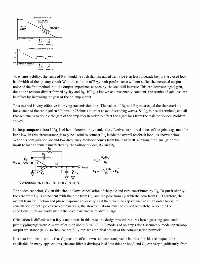
To ensure stability, the value of RX should be such that the added zero (fZ) is at least a decade below the closed loopbandwidth of the op amp circuit.With the addition of RX,circuit performance will not suffer the increased outputnoise of the first method, but the output impedance as seen by the load will increase.This can decrease signal gain,due to the resistor divider formed by RX and RL. If RL is known and reasonably constant, the results of gain loss canbe offset by increasing the gain of the op amp circuit.
This method is very effective in driving transmission lines.The values of RL and RX must equal the characteristicimpedance of the cable (often 50ohms or 75ohms) in order to avoid standing waves. So RX is pre-determined, and allthat remains is to double the gain of the amplifier in order to offset the signal loss from the resistor divider. Problemsolved.
In-loop compensation: If RL is either unknown or dynamic, the effective output resistance of the gain stage must bekept low. In this circumstance, it may be useful to connect RX inside the overall feedback loop, as shown below.With this configuration, dc and low-frequency feedback comes from the load itself, allowing the signal gain frominput to load to remain unaffected by the voltage divider, RX and RL.
The added capacitor, CF, in this circuit allows cancellation of the pole and zero contributed by CL.To put it simply,the zero from CF is coincident with the pole from CL, and the pole from CF with the zero from CL.Therefore, theoverall transfer function and phase response are exactly as if there were no capacitance at all. In order to assurecancellation of both pole/ zero combinations, the above equations must be solved accurately. Also note theconditions; they are easily met if the load resistance is relatively large.
Calculation is difficult when RO is unknown. In this case, the design procedure turns into a guessing game-and aprototyping nightmare.A word of caution about SPICE:SPICE models of op amps don't accurately model open-loopoutput resistance (RO); so they cannot fully replace empirical design of the compensation network.
It is also important to note that CL must be of a known (and constant) value in order for this technique to beapplicable. In many applications, the amplifier is driving a load "outside the box," and CL can vary significantly from

one load to the next. It is best to use the above circuit only when CL is part of a closed system.
One such application involves the buffering or inverting of a reference voltage, driving a large decoupling capacitor.Here, CL is a fixed value, allowing accurate cancellation of pole/zero combinations. The low dc output impedance andlow noise of this method (compared to the previous two) can be very beneficial. Furthermore, the large amount ofcapacitance likely to decouple a reference voltage (often many microfarads) is impractical to compensate by anyother method.
All three of the above compensation techniques have advantages and disadvantages. You should know enough bynow to decide which is best for your application. All three are intended to be applied to "standard", unity gainstable, voltage feedback op amps. Read on to find out about some techniques using special purpose amplifiers.
Q. My op amp has a "compensation" pin. Can I overcompensate the op amp so that it will remain stable whendriving a capacitive load?
A. Yes. This is the easiest way of all to compensate for load capacitance. Most op amps today are internallycompensated for unity-gain stability and therefore do not offer the option to "overcompensate". But many devicesstill exist with inherent stability only at very high noise gains. These op amps have a pin to which an externalcapacitor can be connected in order to reduce the frequency of the dominant pole. To operate stably at lower gains,increased capacitance must be tied to this pin to reduce the gain-bandwidth product. When a capacitive load must bedriven, a further increase (overcompensation) can increase stabilityÑbut at the expense of bandwidth.
Q. So far you've only discussed voltage feedback op amps exclusively, right? Do current feedback (CF) op ampsbehave similarly with capacitive loading? Can I use any of the compensation techniques discussed here?
A. Some characteristics of current feedback architectures require special attention when driving capacitive loads, butthe overall effect on the circuit is the same. The added pole, in conjunction with op-amp output resistance, increasesphase shift and reduces phase margin, potentially causing peaking, ringing, or even oscillation. However, since a CFop amp can't be said to have a "gain-bandwidth product" (bandwidth is much less dependent on gain), stability can'tbe substantially increased simply by increasing the noise gain. This makes the first method impractical. Also, acapacitor (CF) should NEVER be put in the feedback loop of a CF op amp, nullifying the third method. The mostdirect way to compensate a current feedback op amp to drive a capacitive load is the addition of an "out of loop"series resistor at the amplifier output as in method 2.
PartNumber Ch
BWMHz
SRV/ms
vnnV/
Hz
infA/
HzVOSmV
IbnA
SupplyVoltageRange[V]
IQmA
ROohms
CapLoadDrive[pF] Notes
AD817 1 50 350 15 1500 0.5 3000 5-36 7 8 unlim
AD826 2 50 350 15 1500 0.5 3000 5-36 6.8 8 unlim
AD827 2 50 300 15 1500 0.5 3000 9-36 5.25 15 unlim
AD847 1 50 300 15 1500 0.5 3000 9-36 4.8 15 unlim
AD848 1 35 200 5 1500 0.5 3000 9-36 5.1 15 unlim GMIN=5
AD849 1 29 200 3 1500 0.3 3000 9-36 5.1 15 unlim GMIN=25
AD704 4 0.8 0.15 15 50 0.03 0.1 4-36 0.375 10000
AD705 1 0.8 0.15 15 50 0.03 0.06 4-36 0.38 10000
AD706 2 0.8 0.15 15 50 0.03 0.05 4-36 0.375 10000
OP97 1 0.9 0.2 14 20 0.03 0.03 4-40 0.38 10000
OP279 2 5 3 22 1000 4 300 4.5-12 2 22 10000
OP400 4 0.5 0.15 11 600 0.08 0.75 6-40 0.6 10000
AD549 1 1 3 35 0.22 0.5 0.00015 10-36 0.6 4000
OP200 2 0.5 0.15 11 400 0.08 0.1 6-40 0.57 2000
OP467 4 28 170 6 8000 0.2 150 9-36 2 1600
AD744 1 13 75 16 10 0.3 0.03 9-36 3.5 1000 comp.term
AD8013 3 140 1000 3.5 12000 2 3000 4.5-13 3.4 1000 current fb
AD8532 2 3 5 30 50 25 0.005 3-6 1.4 1000
AD8534 4 3 5 30 50 25 0.005 3-6 1.4 1000
OP27 1 8 2.8 3.2 1700 0.03 15 8-44 6.7 70 1000
OP37 1 12 17 3.2 1700 0.03 15 8-44 6.7 70 1000 GMIN=5
OP270 2 5 2.4 3.2 1100 0.05 15 9-36 2 1000
OP470 4 6 2 3.2 1700 0.4 25 9-36 2.25 1000
OP275 2 9 22 6 1500 1 100 9-44 2 1000
OP184 1 4.25 4 3.9 400 0.18 80 4-36 2 1000
OP284 2 4.25 4 3.9 400 0.18 80 4-36 2 1000
OP484 4 4.25 4 3.9 400 0.25 80 4-36 2 1000
OP193 1 0.04 15 65 50 0.15 20 3-36 0.03 1000
OP293 2 0.04 15 65 50 0.25 20 3-36 0.03 1000
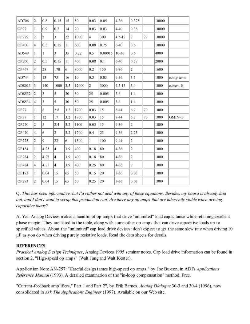
Q. This has been informative, but I'd rather not deal with any of these equations. Besides, my board is already laidout, and I don't want to scrap this production run. Are there any op amps that are inherently stable when drivingcapacitive loads?
A. Yes. Analog Devices makes a handful of op amps that drive "unlimited" load capacitance while retaining excellentphase margin. They are listed in the table, along with some other op amps that can drive capacitive loads up tospecified values. About the "unlimited" cap load drive devices: don't expect to get the same slew rate when driving 10µF as you do when driving purely resistive loads. Read the data sheets for details.
REFERENCESPractical Analog Design Techniques, Analog Devices 1995 seminar notes. Cap load drive information can be found insection 2, "High-speed op amps" (Walt Jung and Walt Kester).
Application Note AN-257: "Careful design tames high-speed op amps," by Joe Buxton, in ADI's ApplicationsReference Manual (1993). A detailed examination of the "in-loop compensation" method. Free.
"Current-feedback amplifiers," Part 1 and Part 2", by Erik Barnes, Analog Dialogue 30-3 and 30-4 (1996), nowconsolidated in Ask The Applications Engineer (1997). Available on our Web site.
Error processing SSI file
Return to Previous PageReturn to Contents PageGo to Next Page
Ask The Applications Engineer—26
by Mary McCarthy & Anthony Collins
SWITCHES AND MULTIPLEXERSQ. Analog Devices doesn’t specify the bandwidth of its ADG series switches and multiplexers. Is there a reason?
A. The ADG series switches and multiplexers have very high input bandwidths, in the hundreds of megahertz.However, the bandwidth specification by itself is not very meaningful, because at these high frequencies, theoff-isolation and crosstalk will be significantly degraded. For example, at 1 MHz, a switch typically has off-isolationof 70 dB and crosstalk of –85 dB. Both off-isolation and crosstalk degrade by 20 dB per decade. This means that at10 MHz, the off-isolation is reduced to 50 dB and the crosstalk increases to –65 dB. At 100 MHz, the off-isolationwill be down to 30 dB while the crosstalk will have increased to –45 dB. So it is not sufficient to consider bandwidthalone—the off-isolation and crosstalk must be considered to determine if the application can tolerate the degradationof these specifications at the required high frequency.
Q. Which switches and multiplexers can be operated with power supplies less than those specified in the data sheet?
A. All of the ADG series switches and multiplexers operate with power supplies down to +5 V or ±5 V. Thespecifications affected by power-supply voltage are timing, on resistance, supply current and leakage current.Lowering power supply voltage reduces power supply current and leakage current. For example, the ADG411’sIS(OFF) and ID(OFF) are ±20 nA, and ID(ON) is ±40 nA, at +125°C with a ±15-V power supply.When the supplyvoltage is reduced to ±5 V, IS(OFF) and ID(OFF) drop to ±2.5 nA, while ID(ON) is reduced to ±5 nA at +125°C.Thesupply currents, IDD, ISS and IL, are 5 mA maximum at +125°C with a ±15-V power supply.When a ±5-V powersupply is used, the supply currents are reduced to 1 µA maximum. The on-resistance and timing increase as thepower supply is reduced. The Figures below show how the timing and on-resistance of the ADG408 vary as afunction of power supply voltage.

Q. Some of the ADG series switches are fabricated on the DI process. What is it?
A. DI is short for dielectric isolation. On the DI process, an insulation layer (trench) is placed between the NMOSand PMOS transistors of each CMOS switch. Parasitic junctions, which occur between the transistors in standardswitches, are eliminated, resulting in a completely latchup-proof switch. In junction isolation (no trench used), the Nand P wells of the PMOS and NMOS transistors form a diode which is reverse-Collins biased in normal operation.However, during overvoltage or power-off conditions,when the analog input exceeds the power supplies, the diode isforward biased, forming a silicon controlled rectifier (SCR)-like circuit with the two transistors, causing the current tobe amplified significantly, leading eventually to latch up.This diode doesn’t exist in dielectrically isolated switches,making the part latchup proof.
Q. How do the fault-protected multiplexers and channel protectors work?
A. A channel of a fault-protected multiplexer or channel protector consists of two NMOS and two PMOStransistors. One of the PMOS transistors does not lie in the direct signal path but, is used to connect the source ofthe second PMOS to its backgate. This has the effect of lowering the threshold voltage, which increases the inputsignal range for normal operation. The source and backgate of the NMOS devices are connected for the same reason.During normal operation, the fault-protected parts operate as a standard multiplexer.When a fault condition occurson the input to a channel, this means that the input has exceeded some threshold voltage which is set by the supplyrail voltages. The threshold voltages are related to the supply rails as follows: for a positive overvoltage, thethreshold voltage is given by VDD – VTN where VTN is the threshold voltage of the NMOS transistor (typically 1.5V).For a negative overvoltage, the threshold voltage is given by VSS – VTP, where VTP is the threshold voltage of thePMOS device (typically 2 V). When the input voltage exceeds these threshold voltages, with no load on the channel,the output of the channel is clamped at the threshold voltage.
Q. How do the parts operate when an overvoltage exists?
A. The next two figures show the operating conditions of the signal path transistors during overvoltage conditions.

This one demonstrates how the series N, P and N transistors operate when a positive overvoltage is applied to thechannel.The first NMOS transistor goes into saturation mode as the voltage on its drain exceeds (VDD – VTN). Thepotential at the source of the NMOS device is equal to (VDD – VTN). The other MOS devices are in a non-saturatedmode of operation.
When a negative overvoltage is applied to a channel,the PMOS transistor enters a saturated mode of operation as thedrain voltage exceeds (VSS – VTP).As with a positive overvoltage, the other MOS devices are non-saturated.
Q. How does loading affect the clamping voltage?
A. When the channel is loaded, the channel output will clamp at a value of voltage between the thresholds. Forexample, with a load of 1 kW,VDD = 15 V, and a positive overvoltage, the output will clamp at VDD–VTN –DV,where DV is due to the IR voltage drop across the channels of the non-saturated MOS devices. In the exampleshown below the voltage at the output of the clamped NMOS is 13.5 V. The on-resistance of the two remainingMOS devices is typically 100 W. Therefore, the current is 13.5 V/(1 kW + 100 W) = 12.27 mA.This produces avoltage drop of 1.2 V across the NMOS and PMOS resulting in a clamp voltage of 12.3 V. The current during a faultcondition is determined by the load on the output, i.e., VCLAMP/RL.
Q.Do the fault-protected multiplexers and channel protectors function when the power supply is absent.
A. Yes.These devices remain functional when the supply rails are down or momentarily disconnected.When VDDand VSS equal 0 V, all the transistors are off, as shown, and the current is limited to sub nanoampere levels.

Q. What is "charge injection"?
A. Charge injection in analog switches and multiplexers is a level change caused by stray capacitance associated withthe NMOS and PMOS transistors that make up the analog switch. The Figure below models the structure of ananalog switch and the stray capacitance associated with such an implementation.The structure basically consists ofan NMOS and PMOS device in parallel. This arrangement produces the familiar "bathtub" resistance profile forbipolar input signals.The equivalent circuit shows the main parasitic capacitances that contribute to the chargeinjection effect, CGDN (NMOS gate to drain) and CGDP (PMOS gate to drain).The gate-drain capacitance associatedwith the PMOS device is about twice that of the NMOS device, because for both devices to have the sameon-resistance, the PMOS device has about twice the area of the NMOS. Hence the associated stray capacitance isapproximately twice that of the NMOS device for typical switches found in the marketplace.
When the switch is turned on, a positive voltage is applied to the gate of the NMOS and a negative voltage is appliedto the gate of the PMOS. Because the stray gate-to-drain capacitances are mismatched, unequal amounts of positiveand negative charge are injected onto the drain.The result is a removal of charge from the output of the switch,manifested as a negative- going voltage spike. Because the analog switch is now turned on this negative charge isquickly discharged through the on resistance of the switch (100 W). This can be seen in the simulation plot at 5ms.Then when the switch is turned off, a negative voltage is applied to the gate of the NMOS and a positive voltageis applied to the gate of the PMOS.The result is charge added to the output of the switch. Because the analog switchis now off, the discharge path for this injected positive charge is a high impedance (100 MW). The result is that theload capacitance stores this charge until the switch is turned on again.The simulation plot clearly shows this with thevoltage on CL (as a result of charge injection) remaining constant at 170 mV until the switch is again turned on at 25ms. At this point an equivalent amount of negative charge is injected onto the output, reducing the voltage on CL to 0V. At 35 ms the switch is turned on again and the process continues in this cyclic fashion.

At lower switching frequencies and load resistance, the switch output would contain both positive and negativeglitches as the injected charge leaks away before the next switch transition.
Q. What can be done to improve the charge injection performance of an analog switch?
A. As noted above, the charge injection effect is caused by a mismatch in the parasitic gate-to-drain capacitance ofthe NMOS and PMOS devices. So if these parasitics can be matched there will be little if any charge injectioneffect.This is precisely what is done in Analog Devices CMOS switches and multiplexers.The matching isaccomplished by introducing a dummy capacitor between the gate and drain of the NMOS device.
Unfortunately the matching is only accomplished under a specific set of conditions, i.e., when the voltage on the

Source of both devices is 0 V.The reason for this is that the parasitic capacitances, CGDN and CGDP, are not constant;they vary with the Source voltage. When the Source voltage of the NMOS and PMOS is varied, their channel depthsvary, and with them, CGDN and CGDP . As a consequence of this matching at VSOURCE= 0 V the charge injectioneffect will be noticeable for other values of VSOURCE.
NOTE: Charge injection is usually specified on the data sheet under these matched conditions, i.e., VSOURCE = 0 V.Under these conditions,the charge injection of most switches is usually quite good in the order of 2 to 3 pC max.However the charge injection will increase for other values ofVSOURCE, to an extent depending on the individualswitch. Many data sheets will show a graph of charge injection as a function of Source voltage.
Q. How do I minimize these effects in my application?
A. The effect of charge injection is a voltage glitch on the output of the switch due to the injection of a fixed amountof charge. The glitch amplitude is a function of the load capacitance on the switch output and also the turn on andturn off times of the switch.The larger the load capacitance, the smaller will be the voltage glitch on the output, i.e.,Q=CxV, or V=Q/C, and Q is fixed. Naturally, it may not always be possible to increase the load capacitance, becauseit would reduce the bandwidth of the channel. However, for audio applications, increasing the load capacitance is aneffective means of reducing those unwanted "pops" and "clicks".
Choosing a switch with a slow turn on and turn off time is also an effective means of reducing the glitch amplitude onthe switch output. The same fixed amount of charge is injected over a longer time period and hence has a longer timeperiod in which to leak away. The result is a wider glitch but much reduced in amplitude.This technique is used quiteeffectively in some of the audio switch products, such as the SSM-2402/ SSM-2412, where the turn on time isdesigned to be of the order of 10 ms.
Another point worth mentioning is that the charge injection performance is directly related to the on-resistance of theswitch. In general the lower the RON, the poorer the charge injection performance.The reason for this is purely due tothe associated geometry, because RON is decreased by increasing the area of the NMOS and PMOS devices, thusincreasing CGDN and CGDP . So trading off RON for reduced charge injection may also be an option in manyapplications.
Q. How can I evaluate the charge injection performance of an analog switch or multiplexer?
A. The most efficient way to evaluate a switch’s charge injection performance is to use a setup similar to the oneshown below. By turning the switch on and off at a relatively high frequency (<10 kHz) and observing the switchoutput on an oscilloscope (using a high impedance probe), a trace similar to that shown in Figure 11 will beobserved.The amount of charge injected into the load is given by DVOUTxCL.Where DVOUT is the output pulseamplitude.

Analog Dialogue 33-2 (1999) 1
Ask the Applications Engineer—27By Bill Englemann
SIGNAL CORRUPTION IN INDUSTRIAL MEASUREMENTQ. What problems am I most likely to run into when instrumenting an
industrial system?
A. The five kinds of problems most frequently reported bycustomers of our I/O Subsystems (IOS) Division are:
1. GROUND LOOPSGround loops are the bane of instrumentation engineers andtechnicians. They cause many lost hours troubleshootingobscure and hard-to-diagnose measurement problems. Dothese symptoms sound familiar?
• Readings slowly drift even though you know the sensor isnot changing.
• Readings shift when another piece of equipment is turned on.
• Measurements differ when a calibration device is connectedat the end of an instrument cable instead of directly at the input.
• A 60-Hz sine wave is superimposed upon your dcmeasurement input.
• There are unexplained measurement equipment failures.
Any of these problems can be caused by ground loops—inadvertent flows of current through “ground,” “common” and“reference” paths connected to points at nominally the samepotential. And all of these problems can be eliminated byisolation, the key signal-conditioning attribute we offer in allour signal conditioning series.
Sometimes separate grounding of two pieces of equipmentintroduces a potential difference and causes current to flowthrough signal lines. Why would this happen if they were bothgrounded? Because the earth and metal structures are actuallyrelatively poor conductors of electricity when compared withthe copper wires that carry power and signals. This inherentresistance to current flow varies with the weather and time ofyear and causes current to flow through any wires that areconnecting the two devices. Many factory and plant buildingsexperience potentials of several tens or hundreds of volts.Appropriate signal conditioning eliminates the possibility ofground loops by electrically isolating the equipment. Signalconditioning will also protect equipment, rejecting potentiallydamaging voltage levels before entering the sensitivemeasurement system.
Isolation provides a completely floating input and output port,where there is no electrical path from field input to output andto power. Hence, there is no path for current to flow, and nopossibility of ground loops.
Q. How is this possible? How can we provide a path for the signal frominput to output, without any path for current to flow?
A. It’s done by magnetic isolation. A representation of the signalis passed through a transformer, which creates a magnetic—not a galvanic—connection. We have perfected the use oftransformers for accurate, reliable low-level signal isolation.This approach employs a modulator and demodulator totransmit the signal across the transformer barrier, and canachieve isolation levels of 2500 volts ac.
One of the most frequently encountered application problemsinvolves measuring a low-level sensor such as a thermocouplein the presence of as much as hundreds of volts of groundpotential. This potential is known as common-mode voltage. Theability of a high-quality signal conditioner to reject errorscaused by common-mode voltage, while still accuratelyamplifying low-level signals is known as common mode rejection(CMR). Our 5B, 6B and 7B Series signal conditioningsubsystems provide sufficient common-mode rejection toreduce the impact of these errors by a factor of 100 million to 1!
2. MISWIRING AND OVERVOLTAGEYou know what happens when a cable from a sensitive dataacquisition board is routed into another cabinet, or anotherpart of the building—the input and output wiring terminalsare grouped among hundreds of other terminals carryingdiverse signals and levels: dc signals, ac signals, milli-voltage,thermocouples, dc power, ac power, proximity switches, relaycircuits, etc. It’s not difficult to imagine even a well trainedtechnician or electrician connecting a wire to the wrongterminal. Wiring diagrams are often updated in real time witha red pen, as system needs change. Equipment gets replacedwith “equivalents.” Sometimes power supplies fail and excessvoltages are applied inadvertently. What can you do to protectyour measurement system?
The answer lies in using rugged signal conditioning onevery analog signal lead. This inexpensive insurance policyprovides protection against miswiring and overvoltage on eachinput and output signal line. For example, the use of a5B Series signal conditioner will provide 240 -V ac of protection,even on input lines used to measure sensitive thermocouplesignals, with levels in the millivolt range. You can literallyconnect a 240-V ac line across the same input lines usedto measure the thermocouple, without any damage. The useof signal conditioning to interface with field I/O will protectall measurement and data acquisition equipment on thesystem side.
3. LOSS OF RESOLUTIONResolution is the smallest change in the measurement that theanalog-digital converter (ADC) system can detect and respondto. For example, if a temperature reading steps from 100.00°to 100.29° to 100.58°, as the actual temperature graduallyincreases through this range, the resolution (least-significant-bit value) is 0.29°. This would occur if you had a signalconditioner measuring a thermocouple with a range of 0° to+1200° and a 12-bit ADC. There are two ways to improve this(make the resolution smaller) and detect smaller changes - usea higher resolution ADC or use a smaller measurement range.
For example, a 15-bit plus sign ADC of the type used in our6B Series would offer resolution of 0.037° on the 0 to 1200°range example, 8 times smaller! On the other hand, if you knewthat most of the time the temperature would be in the vicinityof 100°, you could order from Analog Devices a thermocouplesignal conditioner with a custom range, calibrated for the exactthermocouple type and temperature measurement range. Forexample, a custom-ranged signal conditioner with a span of+50° to +150° would offer resolution of 0.024° with a 12-bitADC, a big improvement over the 0 to 1200° range.

2 Analog Dialogue 33-2 (1999)
4. MULTIPLE SIGNALS DON’T ALL HAVE THESAME PROPERTIESThis can pose quite a challenge to traditional industrialmeasurement approaches where 4, 8 or even 16 channels arededicated to interfacing to the same signal type. For example,let’s say you need to measure two J thermocouples, one 0 to+10 V signal, four 4-20 mA signals and two platinum RTDs(resistance temperature detector). You can either buy individualtransmitters for each channel and then wire them all into acommon 4-20 mA input board, or use a signal conditioningsolution from Analog Devices that is configured channel-by-channel, but is also integrated into a simple backplanesubsystem.
These subsystems incorporate all connections for input, outputand field wiring, as well as simple connections for a dc powersupply. They offer a choice of output options: 0 to +5 V, 0 to+10 V, 4-20 mA and RS-232/485, and more! Input and outputmodules are mix-and-match compatible on a per-channel basisand hot-swappable for the ultimate flexibility.
5. ELECTRICAL INTERFERENCEToday’s industrial factories and plants contain all kinds ofinterference sources: engines and motors, fluorescent lights,two-way radios, generators, etc. Each of these can radiateelectro-magnetic noise that can be picked up by wiring, circuitboards and measurement modules. Even with the best shieldingand grounding practices, this interference can show up as noiseon the signal measurement. How can this be eliminated? Byproviding high noise rejection in the signal conditioningsubsystem.
Lower-frequency noise can be eliminated by choosing signal-conditioning subsystems with excellent common mode andnormal mode rejection. Common mode noise present on boththe plus and minus inputs can be seen when measuring eitherthe plus or minus input with respect to a common point likeground. Normal-mode noise is measured in the differencebetween the plus and minus inputs. A typical common moderejection specification on our signal conditioning subsystemsis 160 dB. This log scale measurement means that the effect of
any common mode voltage noise is reduced relative to signalby a factor of 108, or 100 million to 1!
Very high frequency noise in the radio frequency bands cancause dc offsets due to rectification. It requires otherapproaches, including careful circuit layout and the use of RFIfilters such as ferrite beads. The performance measures areindicated by our compliance with the EN certifications forelectromagnetic susceptibility popularized by the CE markrequirements of the European community. A typical applicationwhere this is important would be where a two-way radio isused within a few feet of the input wiring and signalconditioning subsystem. It is necessary to reject measurementerrors whenever the radios are transmitting. Good panel layoutpractice and the use of signal conditioning will ensure the bestaccuracy in these noisy environments.
CONCLUSIONQ. What are some good installation and wiring practices
A. Here are a few suggestions. You may also want to take a look at“Design Tools” and the Analog Devices book, Practical AnalogDesign Techniques, available for sale in hard copy and free onthe Web.
• Avoid installing sensitive measuring equipment, or wirecarrying low level signals, near sources of electrical andmagnetic noise, such as breakers, transformers, motors, SCRdrives, welders, fluorescent lamp controllers, or relays.
• Use twisted pair wiring to reduce magnetic noise pickup.Look for 10 to 12 twists per foot.
• Use shielded cable with the shield connected to circuitcommon at the input end only.
• Never run signal-carrying wires in the same conduit thatcarries power lines, relay contact leads or other high-levelvoltages or currents.
• In extremely high interference environments, mount signalconditioning and measurement equipment inside groundedand closed metal cabinets.

Analog Dialogue 33-3 (1999) 1
Ask the Applications Engineer—28By Eamon Nash
LOGARITHMIC AMPLIFIERS EXPLAINEDQ. I’ve just been reading data sheets of some recently released Analog
Devices log amps and I’m still a little confused about what exactly alog amp does.
A. You’re not alone. Over the years, I have had to deal with lots ofinquiries about the changing emphasis on functions that logamps perform and radically different design concepts. Let mestart by asking you, what do you expect to see at the output ofa log amp?
Q. Well, I suppose that I would expect to see an output proportional tothe logarithm of the input voltage or current, as you describe in theNonlinear Circuits Handbook| <http://www.analog.com/publications/magazines/Dialogue/Anniversary/books.html> and theLinear Design Seminar Notes| <http://www.analog.com/publications/press/misc/press_123094.html>.
A. Well, that’s a good start but we need to be more specific. Theterm log amp, as it is generally understood in communicationstechnology, refers to a device which calculates the log of aninput signal’s envelope. What does that mean in practice? Takea look a the scope photo below. This shows a 10-MHz sinewave modulated by a 100-kHz triangular wave and the grosslogarithmic response of the AD8307, a 500-MHz 90-dB logamp. Note that the input signal on the scope photo consists ofmany cycles of the 10-MHz signal, compressed together, usingthe time/div knob of the oscilloscope. We do this to show theenvelope of the signal, with its much slower repetition frequencyof 100 kHz. As the envelope of the signal increases linearly, wecan see the characteristic “log (x)” form in the output responseof the log amp. In contrast, if our measurement device were alinear envelope detector (a filtered rectified output), the outputwould simply be a tri-wave.
TIME
VO
LTA
GE
INPUT
OUTPUT
Q. So I don’t see the log of the instantaneous signal?
A. That’s correct, and it’s the source of much of the confusion.The log amp gives an indication of the instant-by-instant low-frequency changes in the envelope, or amplitude, of the signalin the log domain in the same way that a digital voltmeter, setto “ac volts,” gives a steady (linear) reading when the input isconnected to a constant amplitude sine wave and follows any
adjustments to the amplitude. A device that calculates theinstantaneous log of the input signal is quite different, especiallyfor bipolar signals.
On that point, let’s digress for a moment to consider such adevice. Think about what would happen when an ac input signalcrosses zero and goes negative. Remember, the mathematicalfunction, log x, is undefined for x real and less than or equal tozero, or –x greater than or equal to zero (see figure).
SINH–1 (X)
LOG (2X)
–LOG (–2X)
Y
X
However, as the figure shows, the inverse hyperbolic sine,sinh–1 x, which passes symmetrically through zero, is a goodapproximation to the combination of log 2x and minus log(–2x), especially for large values of |x|. And yes, it is possibleto build such a log amp; in fact, Analog Devices many yearsago manufactured and sold Model 752 N & P temperature-compensated log diode modules, which—in complementaryfeedback pairs—performed that function. Such devices, whichcalculate the instantaneous log of the input signal are calledbaseband log amps (the term “true log amp” is also used). Thefocus of this discussion, however, is on envelope-detectinglog amps, also referred to as demodulating log amps, whichhave interesting applications in RF and IF circuitry forcommunications.
Q. But, from what you have just said, I would imagine that a log ampis generally not used to demodulate signals?
A. Yes, that is correct. The term demodulating came to be appliedto this type of device because a log amp recovers the log of theenvelope of a signal in a process somewhat like that ofdemodulating AM signals.
In general, the principal application of log amps is to measuresignal strength, as opposed to detecting signal content. The logamp’s output signal, which can represent a many-decadedynamic range of high-frequency input signal amplitudes by arelatively narrow range, is typically used to regulate gain. Theclassic example of this is using a log amp in an automatic gaincontrol loop, to regulate the gain of a variable-gain amplifier.The receiver of a cellular base station, for example, might usethe signal from a log amp to regulate the receiver gain. Intransmitters, log amps are also used to measure and regulatetransmitted power.
However, there are some applications where a log amp is usedto demodulate a signal. The figure shows a received signal thathas been modulated using amplitude shift keying (ASK). Thissimple modulation scheme, similar to early transmissions ofradar pulses, conveys digital information by transmitting a seriesof RF bursts (logic 1 = burst, logic 0 = no burst). When this
2 Analog Dialogue 33-3 (1999)
signal is applied to a log amp, the output is a pulse train whichcan be applied to a comparator to give a digital output. Noticethat the actual amplitude of the burst is of little importance;we only want to detect its presence or absence. Indeed, it isthe log amp’s ability to convert a signal which varies over alarge dynamic range (10 mV to 1 V in this case) into one thatvaries over a much smaller range (1 V to 3 V) that makes theuse of a log amp so appealing in this application.
LOGAMP
1V2V
3V
10mV100mV
1V
Q. Can you explain briefly how a log amp works?
A. The figure shows a simplified block diagram of a log amp. Thecore of the device is a cascaded chain of amplifiers. Theseamplifiers have linear gain, usually somewhere between 10 dBand 20 dB. For simplicity of explanation, in this example, wehave chosen a chain of 5 amplifiers, each with a gain of 20 dB,or 10×. Now imagine a small sine wave being fed into the firstamplifier in the chain. The first amplifier will amplify the signalby a factor of 10 before it is applied to the second amplifier. Soas the signal passes through each subsequent stage, it isamplified by an additional 20 dB.
Now, as the signal progresses down the gain chain, it will atsome stage get so big that it will begin to clip (the term limit isalso used) as shown. In the simplified example, this clippinglevel (a desired effect) has been set at 1 V peak. The amplifiersin the gain chain would be designed to limit at this same preciselevel.
20dB
DET
20dB
DET
20dB
DET
20dB
DET
20dB
DET
1V1V 1V 1V
VINLIMITEROUTPUT
1V1V1V1V
S
4V
LOWPASS
FILTER
VLOG
After the signal has gone into limiting in one of the stages (thishappens at the output of the third stage in the figure), thelimited signal continues down the signal chain, clipping at eachstage and maintaining its 1 V peak amplitude as it goes.
The signal at the output of each amplifier is also fed into a fullwave rectifier. The outputs of these rectifiers are summedtogether as shown and applied to a low-pass filter, whichremoves the ripple of the full-wave rectified signal. Note thatthe contributions of the earliest stages are so small as to benegligible. This yields an output (often referred to as the “video”output), which will be a steady-state quasi-logarithmic dcoutput for a steady-state ac input signal. The actual devicescontain innovations in circuit design that shape the gain andlimiting functions to produce smooth and accurate logarithmicbehavior between the decade breaks, with the limiter outputsum comparable to the characteristic, and the contribution ofthe less-than-limited terms to the mantissa.
To understand how this signal transformation yields the log ofthe input signal’s envelope, consider what happens if the inputsignal is reduced by 20 dB. As it stands in the figure, theunfiltered output of the summer is about 4 V peak (from 3stages that are limiting and a fourth that is just about to limit).If the input signal is reduced by a factor of 10, the output ofone stage at the input end of the chain will become negligible,and there will be one less stage in limiting. Because of thevoltage lost from this stage, the summed output will drop toapproximately 3 V. If the input signal is reduced by a further20 dB, the summed output will drop to about 2 V.
So the output is changing by 1 V for each factor-of-10 (20-dB)amplitude change at the input. We can describe the log ampthen as having a slope of 50 mV/dB.
Q. O.K. I understand the logarithmic transformation. Now can youexplain what the Intercept is?
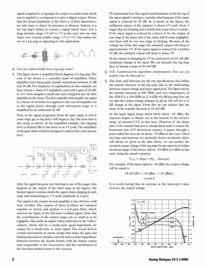
A. The slope and intercept are the two specifications that definethe transfer function of the log amp, that is, the relationshipbetween output voltage and input signal level. The figure showsthe transfer function at 900 MHz, and over temperature, ofthe AD8313, a 100-MHz-to-2.5-GHz 65-dB log amp. You cansee that the output voltage changes by about 180 mV for a 10dB change at the input. From this we can deduce that theslope of the transfer function is 18 mV/dB.
As the input signal drops down below about –65 dBm, theresponse begins to flatten out at the bottom of the device’srange (at around 0.5 V, in this case). However, if the linearpart of the transfer function is extrapolated until it crosses thehorizontal axis (0 V theoretical output), it passes through apoint called the intercept (at about –93 dBm in this case). Oncethe slope and intercept of a particular device are known (thesewill always be given in the data sheet), we can predict thenominal output voltage of the log amp for any input level withinthe linear range of the device (about –65 dBm to 0 dBm in thiscase) using the simple equation:
VOUT = Slope × (PIN – Intercept)
For example, if the input signal is –40 dBm the output voltagewill be equal to
18 mV/dB × (–40 dBm – (–93 dBm))
= 0.95 V
It is worth noting that an increase in the intercept’s valuedecreases the output voltage.
INPUT AMPLITUDE – dBm
2.0
–70
VO
UT –
Vol
ts
1.8
1.6
1.4
1.2
1.0
0.8
0.6
0.4
0.2
0
–60 –50 –40 –30 –20 –10 0 10
VS = +5V5
4
3
2
1
0
–1
–2
–3
–4
–5
ER
RO
R –
dB
+258C
+858C
–408C
ERROR CURVES
–80–90–100
INTERCEPT
Analog Dialogue 33-3 (1999) 3
The figure also shows plots of deviations from the ideal, i.e.,log conformance, at –40°C, +25°C, and +85°C. For example, at+25°C, the log conformance is to within at least ±1 dB for aninput in the range –2 dBm to –67 dBm (over a smaller range,the log conformance is even better). For this reason, we callthe AD8313 a 65-dB log amp. We could just as easily say thatthe AD8313 has a dynamic range of 73 dB for log conformancewithin 3 dB.
Q. In doing some measurements, I’ve found that the output level atwhich the output voltage flattens out is higher than specified in thedata sheet. This is costing me dynamic range at the low end. What iscausing this?
A. I come across this quite a bit. This is usually caused by theinput picking up and measuring an external noise. Rememberthat our log amps can have an input bandwidth of as much as2.5 GHz! The log amp does not know the difference betweenthe wanted signal and the noise. This happens quite a lot inlaboratory environments, where multiple signal sources maybe present. Remember, in the case of a wide-range log amp, a–60-dBm noise signal, coming from your colleague who istesting his new cellular phone at the next lab bench, can wipeout the bottom 20-dB of your dynamic range.
A good test is to ground both differential inputs of the logamp. Because log amps are generally ac-coupled, you shoulddo this by connecting the inputs to ground through couplingcapacitors.
Solving the problem of noise pickup generally requires somekind of filtering. This is also achieved indirectly by using amatching network at the input. A narrow-band matching
network will have a filter characteristic and will also providesome gain for the wanted signal. Matching networks arediscussed in more detail in data sheets for the AD8307,AD8309, and AD8313.
Q. What corner frequency is typically chosen for the output stage’s low-pass filter?
A. There is a design trade-off here. The corner frequency of theon-chip low-pass filter must be set low enough to adequatelyremove the ripple of the full-wave rectified signal at the outputof the summer. This ripple will be at a frequency 2 times theinput signal frequency. However the RC time constant of thelow-pass filter determines the maximum rise time of the output.Setting the corner frequency too low will result in the log amphaving a sluggish response to a fast-changing input envelope.
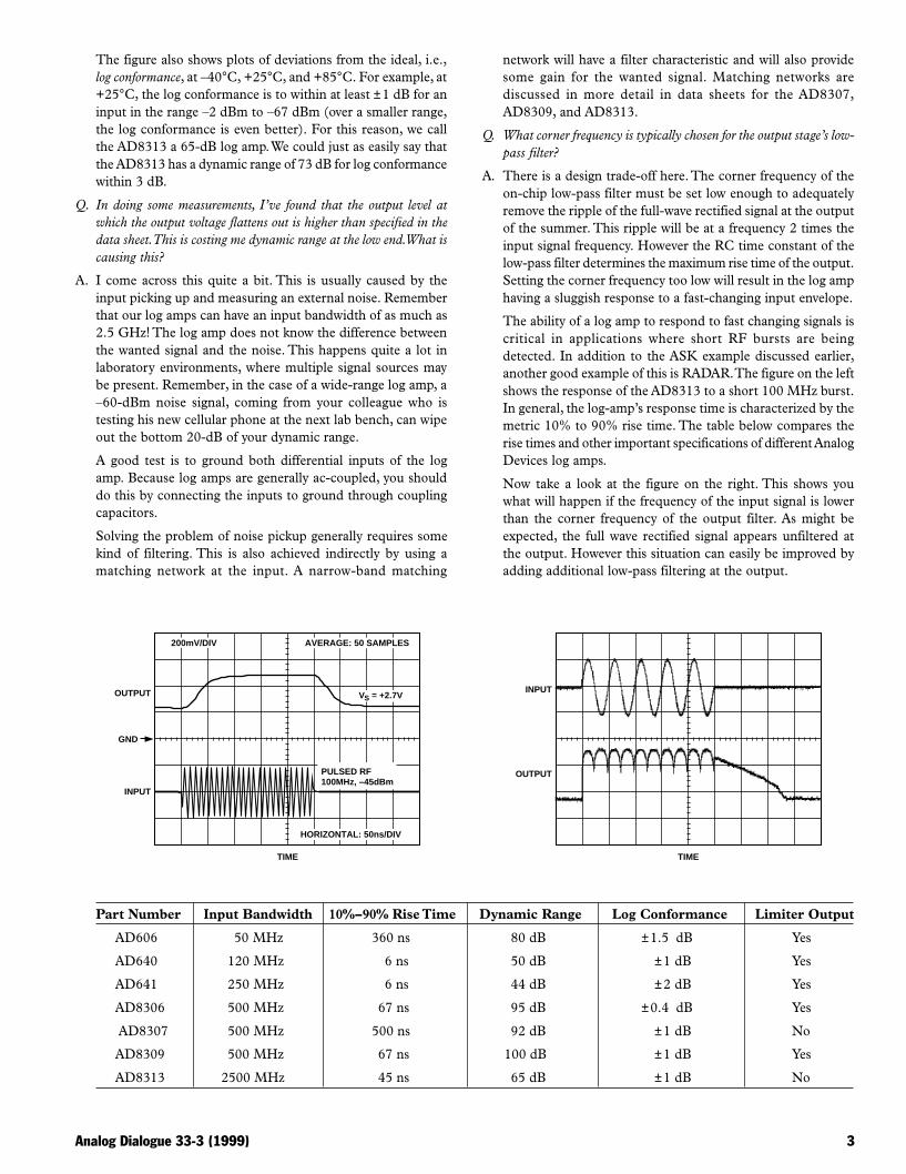
The ability of a log amp to respond to fast changing signals iscritical in applications where short RF bursts are beingdetected. In addition to the ASK example discussed earlier,another good example of this is RADAR. The figure on the leftshows the response of the AD8313 to a short 100 MHz burst.In general, the log-amp’s response time is characterized by themetric 10% to 90% rise time. The table below compares therise times and other important specifications of different AnalogDevices log amps.
Now take a look at the figure on the right. This shows youwhat will happen if the frequency of the input signal is lowerthan the corner frequency of the output filter. As might beexpected, the full wave rectified signal appears unfiltered atthe output. However this situation can easily be improved byadding additional low-pass filtering at the output.
Part Number Input Bandwidth 10%–90% Rise Time Dynamic Range Log Conformance Limiter Output
AD606 50 MHz 360 ns 80 dB ±1.5 dB Yes
AD640 120 MHz 6 ns 50 dB ±1 dB Yes
AD641 250 MHz 6 ns 44 dB ±2 dB Yes
AD8306 500 MHz 67 ns 95 dB ±0.4 dB Yes
AD8307 500 MHz 500 ns 92 dB ±1 dB No
AD8309 500 MHz 67 ns 100 dB ±1 dB Yes
AD8313 2500 MHz 45 ns 65 dB ±1 dB No
GND
HORIZONTAL: 50ns/DIV
VS = +2.7V
PULSED RF100MHz, –45dBm
200mV/DIV AVERAGE: 50 SAMPLES
OUTPUT
INPUT
TIME
INPUT
TIME
OUTPUT

4 Analog Dialogue 33-3 (1999)
Q. I notice that there is an unusual tail on the output signal at theright. What is causing that?
A. That is an interesting effect that results from the nature of thelog transformation that is taking place. Looking again at transferfunction plot (i.e. voltage out vs. input level), we can see thatat low input levels, small changes in the input signal have asignificant effect on the output voltage. For example a changein the input level from 7 mV to 700 µV (or about –30 dBm to–50 dBm) has the same effect as a change in input level from70 mV to 7 mV. That is what is expected from a logarithmicamplifier. However, looking at the input signal (i.e., the RFburst) with the naked eye, we do not see small changes in themV range. What’s happening in the figure is that the burstdoes not turn off instantly but drops to some level and thendecays exponentially to zero. And the log of a decayingexponential signal is a straight line similar to the tail in theplot.
Q. Is there a way to speed up the rise time of the log amp’s output?
A. This is not possible if the internal low-pass filter is buffered,which is the case in most devices. However the figure showsone exception: the un-buffered output stage of the AD8307 ishere represented by a current source of 2 µA/dB, which islooking at an internal load of 12.5 kΩ. The current source andthe resistance combine to give a nominal slope of 25 mV/dB.The 5-pF capacitance in parallel with the 12.5-kΩ resistancecombines to yield a low-pass corner frequency of 2.5 MHz.The associated 10%-90% rise time is about 500 ns.
In the figure, an external 1.37-kΩ shunt resistor has been added.Now, the overall load resistance is reduced to around 1.25 kΩ.This will decrease the rise time ten-fold. However the overalllogarithmic slope has also decreased ten-fold. As a result,external gain is required to get back to a slope of 25 mV/dB.
You may also want to take a look at the Application Note AN-405. This shows how to improve the response time of theAD606.
AD8031
AD8307
12.5kV5pF2mA/dB
1.37kV
23.7kV2.67kV
VOUT
Q. Returning to the architecture of a typical log amp, is the heavilyclipped signal at the end of the gain chain in any way useful?
A. The signal at the end of the linear gain chain has the propertythat its amplitude is constant for all signal levels within thedynamic range of the log amp. This type of signal is very usefulin phase- or frequency demodulation applications. Rememberthat in a phase-modulation scheme (e.g. QPSK or broadcastFM), there is no useful information contained in the signal’samplitude; all the information is contained in the phase. Indeed,amplitude variations in the signal can make the demodulationprocess quite a bit more difficult. So the signal at the output ofthe linear gain chain is often made available to give a limiteroutput. This signal can then be applied to a phase or frequencydemodulator.
The degree to which the phase of the output signal changes asthe input level changes is called phase skew. Remember, thephase between input and output is generally not important. Itis more important to know that the phase from input to outputstays constant as the input signal is swept over its dynamicrange. The figure shows the phase skew of the AD8309’s limiteroutput, measured at 100 MHz. As you can see, the phase variesby about 6° over the device’s dynamic range and overtemperature.
INPUT LEVEL – dBm Re 50 V
10
–60
NO
RM
ALI
ZE
D P
HA
SE
SH
IFT
– D
egre
es
8
6
4
2
0
–10–50 –30 –20 –10 10
–2
–4
–6
–8
–40 0
TA = +858C
TA = +258C
TA = –408C
Q. I noticed that something strange happens when I drive the log ampwith a square wave.
A. Log amps are generally specified for a sine wave input. Theeffect of differing signal waveforms is to shift the effective valueof the log amp’s intercept upwards or downwards. Graphically,this looks like a vertical shift in the log amp’s transfer function(see figure), without affecting the logarithmic slope. The figureshows the transfer function of the AD8307 when alternatelyfed by an unmodulated sine wave and by a CDMA channel (9channels on) of the same rms power. The output voltage willdiffer by the equivalent of 3.55 dB (88.7 mV) over the completedynamic range of the device.
INPUT POWER – dBm
3
–60
OU
TP
UT
VO
LTA
GE
– V
olts
2.5
2
1.5
0–50 –30 –20 –10 10
1
0.5
–40 0–70–80 20
3.55dB (88.7mV)
SINEWAVE
CDMA

Analog Dialogue 33-3 (1999) 5
The table shows the correction factors that should be appliedto measure the rms signal strength of various signal types witha logarithmic amplifier which has been characterized using asine wave input. So, to measure the rms power of a squarewave,for example, the mV equivalent of the dB value given in thetable (–3.01 dB, which corresponds to 75.25 mV in the case ofthe AD8307) should be subtracted from the output voltage ofthe log amp.
Correction FactorSignal Type (Add to Output Reading)
Sine Wave 0 dB
Square Wave or DC –3.01 dB
Triangular Wave +0.9 dB
GSM Channel(All Time Slots On) +0.55 dB
CDMA Forward Link(Nine Channels On) +3.55 dB
Reverse CDMA Channel 0.5 dB
PDC Channel(All Time Slots On) +0.58 dB
Gaussian Noise +2.51 dB
Q. In your data sheets you sometimes give input levels in dBm andsometimes in dBV. Can you explain why?
A. Signal levels in communications applications are usuallyspecified in dBm. The dBm unit is defined as the power in dBrelative to 1 mW i.e.,
Power (dBm) = 10 log10 (Power/1 mW)
Since power in watts is equal to the rms voltage squared, dividedby the load impedance, we can also write this as
Power (dBm) = 10 log10 ((Vrms2/R)/1 mW)
It follows that 0 dBm occurs at 1 mW, 10 dBm corresponds to10 mW, +30 dBm corresponds to to 1 W, etc. Becauseimpedance is a component of this equation, it is alwaysnecessary to specify load impedance when talking about dBmlevels.
50VRIN(HIGH)
Log amps, however fundamentally respond to voltage, not topower. The input to a log amp is usually terminated with anexternal 50-Ω resistor to give an overall input impedance ofapproximately 50 Ω, as shown in the figure (the log amp has arelatively high input impedance, typically in the 300 Ω to1000 Ω range). If the log amp is driven with a 200-Ω signaland the input is terminated in 200 Ω, the output voltage of thelog amp will be higher compared to the same amount of powerfrom a 50-Ω input signal. As a result, it is more useful to workwith the voltage at the log amp’s input. An appropriate unit,therefore, would be dBV, defined as the voltage level in dBrelative to 1 V, i.e.,
Voltage (dBV) = 20 log10 (Vrms/1 V)
However, there is disagreement in the industry as to whetherthe 1-V reference is 1 V peak (i.e., amplitude) or 1 V rms.Most lab instruments (e.g., signal generators, spectrumanalyzers) use 1 V rms as their reference. Based upon this,dBV readings are converted to dBm by adding 13 dB. So–13 dBV is equal to 0 dBm.
As a practical matter, the industry will continue to talk aboutinput levels to log amps in terms of dBm power levels, with theimplicit assumption that it is based on a 50 Ω impedance, evenif it is not completely correct to do so. As a result it is prudentto provide specifications in both dBm and dBV in data sheets.
The figure shows how mV, dBV, dBm and mW relate to eachother for a load impedance of 50 Ω. If the load impedancewere 20 Ω, for example, the V (rms), V (p-p) and dBV scaleswill be shifted downward relative to the dBm and mW scales.Also, the V (p-p) scale will shift relative to the V (rms) scale ifthe peak to rms ratio (also called crest factor) is somethingother than √2 (the peak to rms ratio of a sine wave). b
V (p-p) V (rms) dBV dBm mW
+10
+1
0.1
0.01
10
1
0.1
0.01
0.001 –60
–50
–40
–30
–20
–10
0
+10
+20
–50
–40
–30
–20
–10
0
+10
+20
+30
0.00001
0.0001
0.001
0.01
0.1
1
10
100
1000

Accelerometers—Fantasy & Reality By Harvey Weinberg [[email protected]]
As applications engineers supporting ADI’s compact, low-cost, gravity-sensitive iMEMs® accelerometers, we get to hear lots of creative ideas about how to employ accelerometers in useful ways, but sometimes the suggestions violate physical laws! We’ve rated some of these ideas on an informal scale, from real to dream land:
• Real – A real application that actually works today and is currently in production. • Fantasy – An application that could be possible if we had much better technology. • Dream Land – Any practical implementation we can think of would violate physical laws.
Washing machine load balancing. Unbalanced loads during the high-speed spin-cycle cause washing machines to shake and, if unrestrained, they can even “walk” across the floor. An accelerometer senses acceleration during the spin cycle. If an imbalance is present, the washing machine redistributes the load by jogging the drum back and forth until the load is balanced.
Real. With better load balance, faster spin rates can be used to wring more water out of clothing, making the drying process more energy efficient—a good thing these days! As an added benefit, fewer mechanical components are required for damping the drum motion, making the overall system lighter and less expensive. Correctly implemented, transmission and bearing service life is extended because of lower peak loads present on the motor. This application is in production.
Machine Health Monitors. Many industries change or overhaul mechanical equipment using a calendar-based preventive maintenance schedule. This is especially true in applications where one cannot tolerate unscheduled down-time. So, machinery with plenty of service life left is often prematurely rebuilt at a cost of millions of dollars across many industries. By embedding accelerometers in bearings or other rotating equipment, service life can be extended without risking sudden failure. The accelerometer senses the vibration of bearings or other rotating equipment to determine their condition.
Real. Using the vibration “signature” of bearings to determine their condition is a well proven and industry-accepted method of equipment maintenance, but wide measurement bandwidth is needed for accurate results. Before the release of the ADXL001, the cost of accelerometers and associated signal conditioning equipment had been too high. Now, its wide bandwidth (22 kHz) and internal signal conditioning make the ADXL001 ideal for low-cost bearing maintenance.
Automatic Leveling. Accelerometers measure the absolute inclination of an object, such as a large machine or a mobile home. A microcontroller uses the tilt information to automatically level the object.
Real to Fantasy (depending on the application). Self-leveling is a very demanding application, as absolute precision is required. Surface micromachined accelerometers have impressive resolution, but absolute tilt measurement with high accuracy (better than 1° of inclination) requires temperature stability and hysteresis performance that today’s surface-micromachined accelerometers cannot achieve. In applications where the temperature range is modest, high stability accelerometers like the ADXL203 are up to the task. Applications needing absolute accuracy to within ±5° over a wide temperature range can be handled as well. However more

precise leveling over a wide temperature range requires external temperature compensation. Even with external temperature compensation absolute accuracy of better than ±0.5° of inclination is difficult to achieve. Some applications are currently in production.
Human Interface for Mobile Phones. The accelerometer allows the microcontroller to recognize user gestures, enabling one-handed control of mobile devices.
Real. Mobile phone screens eat up most of the available real estate for controls. Using an accelerometer for user interface functions allows mobile phone makers to add “buttonless” features such as Tap/Double Tap (emulating a mouse click/double click), screen rotation, tilt controlled scrolling, and ringer control based on orientation—to name just a few. In addition, mobile phone makers can use the accelerometer to improve accuracy and usability of navigation functions, and for other new applications. This application is currently in production.
Car Alarm. The accelerometer senses if a car is being jacked up or being picked up by a tow truck, and sets off the alarm.
Real. One of the most popular methods of auto theft is to steal the car by simply towing it away. Conventional car alarms do not protect against this. Shock sensors cannot measure changes in inclination, and ignition-disabling systems are ineffectual. This application takes advantage of the high-resolution capabilities of the ADXL213. If the accelerometer measures an inclination change of more than 0.5° per minute, the alarm is sounded—hopefully scaring off the would-be thief. Good temperature stability is needed as no one wants their car alarm to go off because of changes in the weather, making the highly stable ADXL213 an ideal choice. This application is currently in production in OEM and after-market automotive anti-theft systems.
Ski Bindings. The accelerometer measures the total shock energy and signature to determine if the binding should release.
Fantasy. Mechanical ski bindings are highly evolved, but limited in performance. Measuring the actual shock experienced by the skier would accurately determine if a binding should release. Intelligent systems could take each individual’s capability and physiology into account. This is a practical accelerometer application, but current battery technology makes it impractical. Small, lightweight batteries that perform well at low temperature will eventually enable this application.
Personal Navigation. In this application, position is determined by dead reckoning (double integration of acceleration over time to determine actual position).
Dream Land. Long term integration results in a large error due to the accumulation of small errors in measured acceleration. Double integration compounds the errors (t2). Without some way of resetting the actual position from time to time, huge errors result. This is analogous to building an integrator by simply putting a capacitor across an op amp. Even if an accelerometer’s accuracy could be improved by ten or one hundred times over what is currently available, huge errors would still eventually result. They would just take longer to happen.
Accelerometers can be used with a GPS navigation system when the GPS signals are briefly unavailable. Short integration periods (a minute or so) can give satisfactory results, and clever algorithms can offer good accuracy using alternative approaches. When walking, for example, the body moves up and down with each step. Accelerometers can be used to make very accurate pedometers that can measure walking distance to within ±1%.

Subwoofer Servo Control. An accelerometer mounted on the cone of the subwoofer provides positional feedback to servo out distortion.
Real. Several active subwoofers with servo control are on the market today. Servo control can greatly reduce harmonic distortion and power compression. Servo control can also electronically lower the Q of the speaker/enclosure system, enabling the use of smaller enclosures, as described in Loudspeaker Distortion Reduction, by Richard A. Greiner and Travis M. Sims, Jr., JAES Vol. 32, No. 12. The ADXL193 is small and light; its mass, added to that of the loudspeaker cone, does not change the overall acoustic characteristics significantly.
Neuromuscular Stimulator. This application helps people who have lost control of their lower leg muscles to walk by stimulating muscles at the appropriate time.
Real. When walking, the forefoot is normally raised when moving the leg forward, and then lowered when pushing the leg backward. The accelerometer is worn somewhere on the lower leg or foot, where it senses the position of the leg. The appropriate muscles are then electronically stimulated to flex the foot as required.
This is a classic example of how micromachined accelerometers have made a product feasible. Earlier models used a liquid tilt sensor or a moving ball bearing (acting as a switch) to determine the leg position. Liquid tilt sensors had problems because of sloshing of the liquid, so only slow walking was possible. Ball-bearing switches were easily confused when walking on hills. An accelerometer measures the differential between leg back and leg forward, so hills do not fool the system and no liquid slosh problem exists. The low power consumption of the accelerometer allows the system to work with a small lithium battery, making the overall package unobtrusive. This application is in production.
Car-Noise Cancellation. The accelerometer senses low-frequency vibration in the passenger compartment; the noise-cancellation system nulls it out using the speakers in the stereo system.
Dream Land. While the accelerometer has no trouble picking up the vibration in the passenger compartment, noise cancellation is highly phase dependent. While we can cancel the noise at one location (around the head of the driver, for example), it will probably increase at other locations.
Conclusion Because of their high sensitivity, small size, low cost, rugged packaging, and ability to measure both static and dynamic acceleration forces, surface micromachined accelerometers have made numerous new applications possible. Many of them were not anticipated because they were not thought of as classic accelerometer applications. The imagination of designers now seems to be the limiting factor in the scope of potential applications—but sometimes designers can become too imaginative! While performance improvements continue to enable more applications, it’s wise to try to stay away from “solutions” that violate the laws of physics.
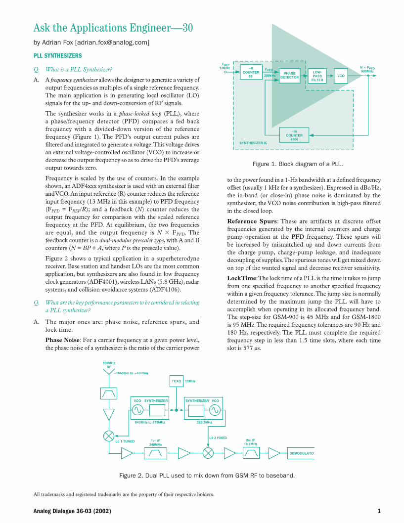
Analog Dialogue 36-03 (2002) 1
Ask the Applications Engineer—30by Adrian Fox [[email protected]]
PLL SYNTHESIZERS
Q. What is a PLL Synthesizer?
A. A frequency synthesizer allows the designer to generate a variety of output frequencies as multiples of a single reference frequency. The main application is in generating local oscillator (LO) signals for the up- and down-conversion of RF signals.
The synthesizer works in a phase-locked loop (PLL), wherea phase/frequency detector (PFD) compares a fed back frequency with a divided-down version of the reference frequency (Figure 1). The PFD’s output current pulses are fi ltered and integrated to generate a voltage. This voltage drives an external voltage-controlled oscillator (VCO) to increase or decrease the output frequency so as to drive the PFD’s average output towards zero.
Frequency is scaled by the use of counters. In the example shown, an ADF4xxx synthesizer is used with an external fi lter and VCO. An input reference (R) counter reduces the reference input frequency (13 MHz in this example) to PFD frequency (FPFD = FREF/R); and a feedback (N) counter reduces the output frequency for comparison with the scaled reference frequency at the PFD. At equilibrium, the two frequenciesare equal, and the output frequency is N FPFD. Thefeedback counter is a dual-modulus prescaler type, with A and B counters (N = BP + A, where P is the prescale value).
Figure 2 shows a typical application in a superheterodyne receiver. Base station and handset LOs are the most common application, but synthesizers are also found in low frequency clock generators (ADF4001), wireless LANs (5.8 GHz), radar systems, and collision-avoidance systems (ADF4106).
Q. What are the key performance parameters to be considered in selecting a PLL synthesizer?
A. The major ones are: phase noise, reference spurs, and lock time.
Phase Noise: For a carrier frequency at a given power level, the phase noise of a synthesizer is the ratio of the carrier power
to the power found in a 1-Hz bandwidth at a defi ned frequency offset (usually 1 kHz for a synthesizer). Expressed in dBc/Hz, the in-band (or close-in) phase noise is dominated by the synthesizer; the VCO noise contribution is high-pass fi ltered in the closed loop.
Reference Spurs: These are artifacts at discrete offset frequencies generated by the internal counters and charge pump operation at the PFD frequency. These spurs will be increased by mismatched up and down currents from the charge pump, charge-pump leakage, and inadequate decoupling of supplies. The spurious tones will get mixed down on top of the wanted signal and decrease receiver sensitivity.
Lock Time: The lock time of a PLL is the time it takes to jump from one specifi ed frequency to another specifi ed frequency within a given frequency tolerance. The jump size is normally determined by the maximum jump the PLL will have to accomplish when operating in its allocated frequency band. The step-size for GSM-900 is 45 MHz and for GSM-1800 is 95 MHz. The required frequency tolerances are 90 Hz and 180 Hz, respectively. The PLL must complete the required frequency step in less than 1.5 time slots, where each time slot is 577 µs.
All trademarks and registered trademarks are the property of their respective holders.
Figure 2. Dual PLL used to mix down from GSM RF to baseband.
Figure 1. Block diagram of a PLL.
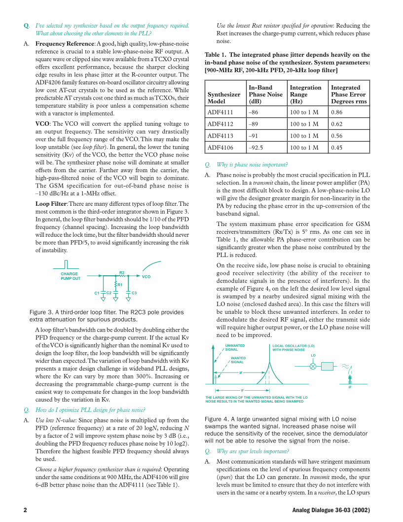
2 Analog Dialogue 36-03 (2002)
Q. I’ve selected my synthesizer based on the output frequency required. What about choosing the other elements in the PLL?
A. Frequency Reference: A good, high quality, low-phase-noise reference is crucial to a stable low-phase-noise RF output. A square wave or clipped sine wave available from a TCXO crystal offers excellent performance, because the sharper clocking edge results in less phase jitter at the R-counter output. The ADF4206 family features on-board oscillator circuitry allowing low cost AT-cut crystals to be used as the reference. While predictable AT crystals cost one third as much as TCXOs, their temperature stability is poor unless a compensation scheme with a varactor is implemented.
VCO: The VCO will convert the applied tuning voltage to an output frequency. The sensitivity can vary drastically over the full frequency range of the VCO. This may make the loop unstable (see loop filter). In general, the lower the tuning sensitivity (Kv) of the VCO, the better the VCO phase noise will be. The synthesizer phase noise will dominate at smaller offsets from the carrier. Farther away from the carrier, the high-pass-filtered noise of the VCO will begin to dominate. The GSM specification for out-of-band phase noise is–130 dBc/Hz at a 1-MHz offset.
Loop Filter: There are many different types of loop filter. The most common is the third-order integrator shown in Figure 3. In general, the loop filter bandwidth should be 1/10 of the PFD frequency (channel spacing). Increasing the loop bandwidth will reduce the lock time, but the filter bandwidth should never be more than PFD/5, to avoid significantly increasing the risk of instability.
Figure 3. A third-order loop filter. The R2C3 pole provides extra attenuation for spurious products.
A loop filter’s bandwidth can be doubled by doubling either the PFD frequency or the charge-pump current. If the actual Kv of the VCO is significantly higher than the nominal Kv used to design the loop filter, the loop bandwidth will be significantly wider than expected. The variation of loop bandwidth with Kv presents a major design challenge in wideband PLL designs, where the Kv can vary by more than 300%. Increasing or decreasing the programmable charge-pump current is the easiest way to compensate for changes in the loop bandwidth caused by the variation in Kv.
Q. How do I optimize PLL design for phase noise?
A. Use low N-value: Since phase noise is multiplied up from the PFD (reference frequency) at a rate of 20 logN, reducing N by a factor of 2 will improve system phase noise by 3 dB (i.e., doubling the PFD frequency reduces phase noise by 10 log2). Therefore the highest feasible PFD frequency should always be used.
Choose a higher frequency synthesizer than is required: Operating under the same conditions at 900 MHz, the ADF4106 will give 6-dB better phase noise than the ADF4111 (see Table 1).
Use the lowest Rset resistor specified for operation: Reducing the Rset increases the charge-pump current, which reduces phase noise.
Table 1. The integrated phase jitter depends heavily on the in-band phase noise of the synthesizer. System parameters: [900-MHz RF, 200-kHz PFD, 20-kHz loop filter]
Synthesizer Model
In-Band Phase Noise(dB)
Integration Range(Hz)
Integrated Phase ErrorDegrees rms
ADF4111 –86 100 to 1 M 0.86
ADF4112 –89 100 to 1 M 0.62
ADF4113 –91 100 to 1 M 0.56
ADF4106 –92.5 100 to 1 M 0.45
Q. Why is phase noise important?
A. Phase noise is probably the most crucial specification in PLL selection. In a transmit chain, the linear power amplifier (PA) is the most difficult block to design. A low-phase-noise LO will give the designer greater margin for non-linearity in the PA by reducing the phase error in the up-conversion of the baseband signal.
The system maximum phase error specification for GSM receivers/transmitters (Rx/Tx) is 5° rms. As one can see in Table 1, the allowable PA phase-error contribution can be significantly greater when the phase noise contributed by the PLL is reduced.
On the receive side, low phase noise is crucial to obtaining good receiver selectivity (the ability of the receiver to demodulate signals in the presence of interferers). In the example of Figure 4, on the left the desired low level signal is swamped by a nearby undesired signal mixing with the LO noise (enclosed dashed area). In this case the filters will be unable to block these unwanted interferers. In order to demodulate the desired RF signal, either the transmit side will require higher output power, or the LO phase noise will need to be improved.
Figure 4. A large unwanted signal mixing with LO noise swamps the wanted signal. Increased phase noise will reduce the sensitivity of the receiver, since the demodulator will not be able to resolve the signal from the noise.
Q. Why are spur levels important?
A. Most communication standards will have stringent maximum specifications on the level of spurious frequency components (spurs) that the LO can generate. In transmit mode, the spur levels must be limited to ensure that they do not interfere with users in the same or a nearby system. In a receiver, the LO spurs

Analog Dialogue 36-03 (2002) 3
can significantly reduce the ability to demodulate the mixed-down signal. Figure 4 shows the effect of reciprocal mixing where the desired signal is swamped with noise due to a large undesired signal mixing with noise on the oscillator. The same effect will occur for spurious noise components.
A high level of spurs can indirectly affect lock time by forcing the designer to narrow the loop bandwidth—slowing response—in order to provide sufficient attenuation of these unwanted components. The key synthesizer specifications to ensure low reference spurs are low charge-pump leakage and matching of the charge pump currents.
Q. Why is lock time important?
A. Many systems use frequency hopping as a means to protect data security, avoid muti-path fading, and avoid interference. The time spent by the PLL in achieving frequency lock is valuable time that cannot be used for transmitting or receiving data; this reduces the effective data rate achievable. Currently there is no PLL available than can frequency-hop quickly enough to meet the timing requirements of the GSM protocol. In base-station applications, two separate PLL devices are used in parallel to reduce the number of wasted slots. While the first is generating the LO for the transmitter, the second PLL is moving to the next allocated channel. In this case a super-fast (<10-µs) settling PLL would significantly reduce the bill of materials (BOM) and layout complexity.
Q. How do I minimize lock time?
A. By increasing the PFD frequency. The PFD frequencydetermines the rate at which a comparison is made between the VCO/N and the reference signal. Increasing the PFD frequency increases the update of the charge pump and reduces lock time. It also allows the loop bandwidth to be widened.
Figure 5. Loop bandwidth has a significant effect on the lock time. The wider the loop bandwidth, the faster the lock time, but also the greater the level of spurious components. Lock time to 1 kHz is 142 µs with a 35-kHz LBW—and 248 µs with a 10-kHz LBW.
Loop Bandwidth. The wider the loop bandwidth, the faster the lock time. The trade-off is that a wider loop bandwidth will reduce attenuation of spurious products and increase the integrated phase noise. Increasing the loop bandwidth significantly (>PFD/5) may cause the loop to become unstable and permanently lose lock. A phase margin of 45 degrees produces the optimum settling transient.
Avoid tuning voltages nearing ground or Vp. When the tuning voltage is within a volt of the rails of the charge pump supply (Vp), the charge pump begins to operate in a saturation region.
Operation in this region will degrade settling time significantly; it may also result in mismatch between jumping-up in frequency and jumping down. Operation in this saturation region can be avoided by using the maximum Vp available or using an active loop filter. Using a VCO with a higher Kv will allow Vtune to remain closer to Vp/2 while still tuning over the required frequency range.
Choose plastic capacitors. Some capacitors exhibit a dielectric memory effect, which can impede lock time. For fast phase locking applications ‘plastic-film’ Panasonic ECHU capacitors are recommended.
Q. What factors determine the maximum PFD frequencyI can use?
A. In order to obtain contiguous output frequencies in steps of the PFD frequency
FPFD <
VCO Output Frequency(P2 − P)
where P is the prescaler value.
The ADF4xxx offers prescaler selections as low as 8/9. This permits a higher PFD frequency than many competitive parts, without violating the above rule—enabling lower phase noise PLL design. Even if this condition is not met, the PLL will lock if B > A and B > 2 in the programming registers.
Q. Fractional-N has been around since 1970. What are its advantages to PLL designers?
A. The resolution at the output of an integer-N PLL is limited to steps of the PFD frequency. Fractional-N allows the resolution at the PLL output to be reduced to small fractions of the PFD frequency. It is possible to generate output frequencies with resolutions of 100s of Hz, while maintaining a high PFD frequency. As a result the N-value is significantly less than for integer-N. Since noise at the charge pump is multiplied up to the output at a rate of 20 logN, significant improvements in phase noise are possible. For a GSM900 system, the fractional-N ADF4252 offers phase noise performance of –103 dBc/Hz, compared with –93 dBc/Hz for the ADF4106 integer-N PLL.
Also offering a significant advantage is the lock-time improvement made possible by fractional-N. The PFD frequency set to 20 MHz and loop bandwidth of 150 kHz will allow the synthesizer jump 30 MHz in <30 µs. Current base stations require 2 PLL blocks to ensure that LOs can meet the timing requirements for transmissions. With the super-fast lock times of fractional-N, future synthesizers will have lock time specs that allow the 2 “ping-pong” PLLs to be replaced with a single fractional-N PLL block.
Q. If fractional-N offers all these advantages, why are integer-N PLLs still so popular?
A. Spurious levels! A fractional-N divide by 19.1 consists of the N-divider dividing by nineteen 90% of the time, and by twenty 10% of the time. The average division is correct, but the instantaneous division is incorrect. Because of this, the PFD and charge pump are constantly trying to correct for instantaneous phase errors. The heavy digital activity of the sigma-delta modulator, which provides the averaging function, creates spurious components at the output. The

4 Analog Dialogue 36-03 (2002)
digital noise, combined with inaccuracies in matching the hard-working charge pump, results in spurious levels greater than those allowable by most communications standards. Only recently have fractional-N parts, such as the ADF4252, made the necessary improvements in spurious performance to allow designers to consider their use in traditional integer-N markets.
Q. What PLL devices have you released recently, how do they differ, and where would I use them?
A. ADF4001 is a <200-MHz PLL, pin-compatible with the popular ADF4110 series, but with the prescaler removed. Applications are stable reference clock generators, in cases where all clocks must be synchronized with a single reference source. They are generally used with VCXOs (voltage-controlled crystal oscillators), which have lower gain (Kv) and better phase noise than VCOs.
ADF4252 is a dual fractional-N device with <70 dBc spurious. It offers <20-µs lock times vs. 250 µs for integer-N, with<100 dBc/Hz phase noise due to the high PFD frequency—a ground-breaking product with a software-programmabletrade-off between phase noise and spurs.
ADF4217L/ADF4218L/ADF4219L are low-phase-noiseupgrades for the LMX2331L/LMX2330L/LMX2370. They consume only 7.1 mA, with a 4-dB improvement in phase noise over competitive devices. Great news for handset designers!
ADF4106 is a 6-GHz PLL synthesizer. Ideal for WLAN equipment in the 5.4-to-5.8-GHz frequency band, it is the lowest-noise integer-N PLL on the market.
Q. What tools are available to simulate loop behavior?
A. ADIsimPLL is a simulation tool developed with Applied Radio Labs. It consists of extensive models for the ADI synthesizers as well as popular VCOs and TCXOs. It allows the user to design passive and active loop filters in many configurations, simulate VCO, PLL, and reference noise, and model spurious and settling behavior. Once a design is completed, a custom evaluation board may be ordered based on the design using an internal weblink to Avnet.
(a) (b)
Figure 6. Lock time and phase noise are just two parame-ters that can be modeled by ADIsimPLL. While phase noise is reduced by >8 dB, the wider loop bandwidths and high PFD frequency allowed by fractional-N reduce the lock time to <30 µs for 30-MHz jumps (as shown).
The tool is free and may be downloaded from www.analog.com/pll. Also widely used are the commercially available Eagleware and MATLAB tools.
Q. Do ADI proprietary parts have specific advantages over comparable competitive parts?
A. Phase noise is the critical specification for many system designers. Phase-noise performance in the ADF4113 family is typically 6 dB better than the National equivalent and>10 dB better than Fujitsu or Philips equivalents. The extended choice of prescaler settings protects the designer from being compromised in selecting a higher PFD frequency by the‘P2 – P’ rule. Another major advantage is the choice of eight programmable charge-pump currents; in wideband designs where the gain of the VCO changes dramatically, the programmable currents can be adjusted to ensure loop stability and bandwidth consistency across the entire band.
Q. What is the future direction of the PLL industry?
A. While chipset solutions are prominent in the headlines, particularly for GSM, the new generation of cellular phone and base stations are still likely to initially favor discrete solutions. Discrete PLL and VCO modules offer improved noise performance and isolation, and are already in high volume production at the start of the design cycle.
The demand for reduced size and current consumption in handsets has driven the development of the ADI L-series of dual synthesizers on 0.35-µm Bi-CMOS in miniature CSP packages. Integrated VCO and PLL modules will be a major growth in newer system designs, where board area and cost reduction of an initial design is crucial.
However the most exciting developments are likely to be in fractional-N technology. Recent improvements in spur performance have allowed the release of the ADF4252 and created unprecedented interest. The phase-noise improvement, super-fast lock times, and versatility inherent in the architecture are likely to dominate LO blocks of future multi-standard high-data-rate wireless systems.
AcknowledgementsThe author would like to thank Mike Curtin, Brendan Daly, and Ian Collins for their valuable contributions.
REFERENCES
(1) “Fractional-N Synthesizers,” (Design Feature), Microwaves and RF, August 1999.
(2) Microwave and RF Wireless Systems, by David M. Pozar.Wiley (2000).
(3) “Phase locked loops for high frequency receivers and transmitters,” by Mike Curtin and Paul O’Brien. Analog Dialogue Volume 33, 1999.
(4) Phase-locked Loops, by Roland E. Best. McGraw-Hill (1993).
(5) “Phase Noise Reference” (Application Note), Applied Radio Labs. b

Analog Dialogue 37-April (2003) 1
Ask The Applications Engineer—31 By Reza Moghimi [[email protected]]
AMPLIFIERS AS COMPARATORS?
Q. What is a comparator? How does it differ from an op amp?
A. The basic function of a high-gain comparator is to determine whether an input voltage is higher or lower than a reference voltage—and to present that decision as one of two voltage levels, established by the output’s limiting values. Comparators have a variety of uses, including: polarity identification, 1-bit analog-to-digital conversion, switch driving, square/triangular-wave generation, and pulse-edge generation.
In principle, any high-gain amplifier can be used to perform this simple decision. But “the devil is in the details.” So there are some basic differences between devices designed as op amps and devices designed to be comparators. For example, for use with digital circuitry, many comparators have latched outputs, and all are designed to have output levels compatible with digital voltage-level specifications. There are some more differences of importance to designers—they will be discussed here.
Q. What are some circumstances where one can go either way?
A. Amplifiers should be considered for use as comparators in applications where low offset and drift, and low bias current, are needed—combined with low cost. On the other hand, there are many designs where an amplifier could not be considered as a comparator because of its lengthy recovery time from output saturation, its long propagation delay, and the inconvenience of making its output compatible with digital logic. Additionally, dynamic stability is a concern.
However, there are cost and performance benefits in using amplifiers as comparators—if their similarities and differences are clearly understood, and the application can tolerate the generally slower speed of amplifiers. No one can claim that an amplifier will serve as a drop-in replacement for a comparator in all cases—but for slow-speed situations requiring highly precise comparison, the performance of some newer amplifiers cannot be matched by that of comparators having greater noise and offset. In some applications with slowly changing inputs, noise will cause comparator outputs to slew rapidly back and forth (see “Curing comparator instability with hysteresis,” Analog Dialogue, Volume 34, 2000). In addition, there can be savings in cost or valuable printed-circuit-board (PCB) area in applications where a dual op amp could be used instead of an op amp and a comparator—or in a design where three of the four amplifiers in a quad package are already committed, and two dc or slowly varying signals must be compared.
Q. Can that fourth amplifier be used as a comparator?
A. This is a question that many system designers are asking us these days. It would pointless to buy a quad op amp, use only three channels, and then buy a separate comparator—if indeed that amplifier could be used in a simple way for the comparison function. Be clear, though, that an amplifier can’t be used as a comparator interchangeably in all cases. For example, if the application requires comparison of signals in less than a microsecond, adding a comparator is probably the only way to go. But if you understand the internal architectural differences between an amplifier and a comparator, and how these differences affect the performance of these ICs in applications, you may be able to obtain the inherent efficiency of using a single chip.
In these pages, we will describe the parametric differences between these two branches of IC amplifier technology and provide useful hints for using an amplifier as a comparator.
Q. So how do amplifiers and comparators differ?
A. Overall, the operational amplifier (op amp) is optimized to provide accuracy and stability (both dc and dynamic) for a specified linear range of output values in precision closed-loop (feedback) circuits. However, when an open-loop amplifier is used as a comparator, with its outputs swinging between their limits, its internal compensation capacitance—used to provide dynamic stability—causes the output to be slow to come out of saturation and slew through its output range. Comparators, on the other hand, are generally designed to operate open loop, with outputs slewing between specified upper and lower voltage limits in response to the sign of the net difference between the two inputs. Since they do not require the op amp’s compensation capacitors, they can be quite fast.
If the input voltage to a comparator is more positive than the reference voltage plus the offset—VOS (with zero reference, it’s just the offset) plus the required overdrive (due to limited gain and output nonlinearity), a voltage corresponding to logic “1” appears at the output. The output will be at logic “0” when the input is less than VOS and the required overdrive. In effect, a comparator can be thought of as a one-bit analog-to-digital converter.
There are different ways of specifying a comparator and an amplifier. As an example, in an amplifier, the offset voltage is the voltage that must be applied to the input to drive the output to a specified mid-range value corresponding to ideal zero input. In a comparator this definition is modified to center in the specified voltage range between 1 and 0 at the output. The comparator’s “low” output value (logic 0) is specified at less than 0.4 V max in comparators with TTL-compatible outputs, while for a low-voltage amplifier, the low output value is very close to its negative rail (e.g., 0 V in a single-supply system). Figure 1 compares the low output values of typical amplifier and comparator models, with a –1-mV differential input applied to each.
2
V391.001V
+
U18AMPLIFIER
V+
V–
3
V381V
+ 1 62.82pV
R1110k
VCC
4
31
7
2
V+
V–
OUT
U20A
VCC VCC
+
–
R1210k
284.12mV
COMPARATORV401.001V
+
V411V
+
Figure 1. Responses of single-supply amplifier (63 pV) and comparator (280 mV) models to a –1-mV input-voltage difference.
Built to compare two levels as quickly as possible, comparators do not have the internal compensation capacitor (“Miller” capacitor) usually found in op amps, and their output circuit is capable of more flexible excitation than that of op amps. This absence of compensation circuitry gives comparators very wide bandwidth. At the output, ordinary op amps use push-pull output circuitry for essentially symmetrical swings between the specified power supply voltages, while comparators usually have an “open-collector” output with grounded emitter. This means that the output of a comparator can be returned through a low-value collector load resistor (“pullup” resistor) to a voltage different from the main positive supply. This feature allows the comparator to interface with a variety

2 Analog Dialogue 37-April (2003)
of logic families. Using a low value of pull-up resistance yields improved switching speed and noise immunity—but at the expense of increased power dissipation.
Because comparators are rarely configured with negative feedback, their (differential) input impedance is not multiplied by loop gain, as is characteristic of op amp circuits. As a result, the input signal sees a changing load and changing (small) input current as the comparator switches. Therefore, under certain conditions, the driving-point impedance must be considered. While negative feedback keeps amplifiers within their linear output region, thus maintaining little variation of most internal operating points, positive feedback is often used to force comparators into saturation (and provide hysteresis to reduce noise sensitivity). A comparator’s input usually accommodates large signal swings, while its output has a limited range due to interfacing requirements, so a lot of rapid level shifting is required within the comparator.
Each of the above differences between an amplifier and a comparator is there for a reason, with the major goal of comparing rapidly varying signals as quickly as possible. But, for comparing slow-speed signals—especially where sub-mV resolution is required—some new rail-to-rail amplifiers from Analog Devices could be better buys than comparators.
Q. OK. I can see that there are overall differences. How do they look to the designer who wants to use an op amp to replace a comparator?
A. Here are six major points:
1. Consider VOS and IB non-linearity vs. input common-mode voltage When using voltage comparators, it is common practice to
ground one input terminal and use a single ended input. The primary reason has been the poor common-mode rejection of the input stage. In contrast, many amplifiers have very high common mode rejection and are capable of detecting microvolt-level differences in the presence of large common-mode signals. Figure 2 shows the response of an AD8605 op amp to a 100-mV differential step riding on a 3-V common-mode voltage.
2
V63V
+
AD8605
V+
V–
3+
–
1 VOUT
V
R1100k
VCC
0
6
4
2
VO
LTS
0
–21 2 3 4 5
TIME (s)
AD8605 WITH 3VCOMMON MODE
Figure 2. Response of open-loop AD8605 to a 100-mV differential step with 3-V common-mode voltage. Note the essentially linear slewing between the 0- and 5-V rails, and the clean saturation.
But, for many rail-to-rail-input amplifiers, input offset voltage (VOS) and input bias current (IB) are non-linear over the input common-mode voltage range. With these amplifiers, the user needs to take this variation into account in the design. If the threshold is set at zero common-mode, but the part is used at some other common-mode level, then the logic level that results may not be as anticipated. For example, a part with offset of 2 mV at zero common mode, and 5-to-6 mV over the entire common mode range may give an erroneous output when comparing a difference of 3 mV at some levels in that range.
2. Watch out for input protection diodes Many amplifiers have protection circuitry at their inputs.
When the two inputs experience a differential voltage greater than a nominal diode drop (say, 0.7 V), the protection diodes start conducting and the input breaks down. Therefore, it is critical to look at the input structure of an amplifier and make sure that it can accommodate the expected range of input signals. Some amplifiers, such as the OP777/OP727/OP747, do not have protection diodes; their inputs can accommodate differential signals up to the supply voltage levels. Figure 3 shows the response to a large differential signal at the input of an OP777. Many amplifiers’ inputs break down under this condition, while the OP777 responds correctly. CMOS-input amplifiers do not have protection diodes at their input, and their input differential voltage can swing rail-to-rail. But remember that, in some cases, applying a large differential signal at the input causes significant shifts of amplifier parameters.
0
6
4
2
VO
LTS
0
–21 2 3 4 5
TIME (s)
VOUT
VIN
2
0.5V+
U37OP777
V+
V–
3
1
V
R27100k
VCC2
V
+VIN
–
Figure 3. Response of an OP777 amplifier to a ±2-V, 1-kHz signal, biased by +2V, and compared with a +0.5-V dc level. Note that there is no phase inversion for this large swing. However, the gain is quite low at a common-mode level of +0.5 V from the negative rail, as can be seen by the approxi-mately 0.3-V overdrive that is needed.
3. Watch out for input voltage range specs and phase-reversal tendencies
Unlike operational amplifiers that usually operate with the input voltages at the same level, comparators typically see large differential voltage swings at their inputs. But some comparators without rail-to-rail inputs are specified to have a limited common-mode input voltage range. If the inputs

Analog Dialogue 37-April (2003) 3
exceed a device’s specified common-mode range (even though within the specified signal range), the comparator may respond erroneously. This may also be true for some of the older types of amplifiers designed with junction-FET (JFET) and bipolar technologies. As the input common-mode voltage exceeds a certain limit (IVR), the output goes through phase inversion. This phenomenon can be detrimental (see in Chapter 6 of Ask the Applications Engineer,* the figure that follows the table). Therefore, it is absolutely critical to pick an amplifier that does not exhibit phase reversal when overdriven. This is one type of problem that can be overcome by using amplifiers with rail-to-rail-inputs.
4. Consider saturation recovery Typical op amps are not designed to be used as fast comparators,
so individual gain stages will go into saturation when the amplifier output is driven to one of its extremes, charging the compensation capacitor and parasitic capacitances. A design difference between amplifiers and comparators is the addition of clamp circuitry in comparators to prevent internal saturation. When an amplifier is pushed into saturation, it takes time for it to recover and then slew to its new final output value—depending on the output structure and the compensation circuitry. Because of the time it takes to come out of saturation, an amplifier is slower when used as comparator than when it is used under control in a closed-loop conf iguration. One can f ind saturation-recovery information in many amplifier data sheets. Figure 4 shows saturation recovery plots for two popular amplifiers (AD8061 and AD8605). The output structures of these amplifiers are standard push-pull rail-to-rail common-emitter.
2.5V
1.0V
0V
200180160140120100806040200TIME (ns)
VOUT
VIN
VS = 2.5VG = 5RL = 1k
500mV/DIV
AD8061. OUTPUT OVERLOAD RECOVERY, INPUT STEP = 0V TO 1V
0V
0V
+2.5V
–50mV
TIME (400ns/DIV)
AD8605. NEGATIVE OVERLOAD RECOVERYVS = 2.5VRL = 10kAV = 100VIN = 50mV
Figure 4. Recovery of two popular amplifiers in closed-loop configuration.
5. Pay attention to factors affecting transition time Speed is one of the distinguishing differences between amplifier
and comparator families. Propagation delay is the time it takes for a comparator to compare two signals at its input, and for its output to reach the midpoint between the two output logic levels. Propagation delay is usually specified with an overdrive, which is the voltage difference between the applied input voltage and the reference that is required for switching within a given time. In the following graphs, the responses of several rail-to-rail CMOS amplifiers are compared with a popular comparator. All amplifiers are configured as shown in Figure 5(a-e) with applied voltage, VIN, = ±0.2 V, centered around 0 V. In the case of the comparator, a 10-k pullup is used instead of a load to ground. The amplifier speeds differ widely, but because of saturation and their lower slew rate, all are much slower than the comparator.
V
4
V11U12
V+
V–
3+
–
1
R6100k
VCC
Figure 5a. Amplifier circuit.
0 5 10 15 20 25
8
4
VO
LTS
0
–430
TIME (s)
LM139
AD8515
AD8541
VIN
AD8601
SLEWING
SATURATIONREGION
Figure 5b. Positive step.
0 5 10 15 20 25
6
4
VO
LTS
2
0
–230
TIME (s)
AD8515
AD8541
VIN
AD8601
LM139
Figure 5c. Negative step.
*www.analog.com/library/analogDialogue/Anniversary/6.html

4 Analog Dialogue 37-April (2003)
0 10 20 30 40
8
VO
LTS
4
0
–450
TIME (s)
LM139
AD8541
VIN
AD8601
AD8515
Figure 5d. Positive step.
0 10 20 30 40
6
4
VO
LTS
2
0
–250
TIME (s)
AD8541
VIN
AD8515
LM139
AD8601
Figure 5e. Negative step.
Figure 5. Responses of comparator and three open-loop amplifier models compared, 0.2-V drive. a. Amplifier circuit configuration. b. Positive step. c. Negative step. Then, with 50-mV signal applied and overdrive of 20 mV. Period = 10 s. d. Positive step. e. Negative step.
Part Supply Offset Supply SlewNumber Current (A) Voltage (mV) Range (V) Rate (V/s)AD8515 350 5.00 1.8–5.0 5AD8601 1,000 0.05 2.7–5.0 4AD8541 55 6.00 2.7–5.0 3AD8061 8,000 6.00 2.7–8.0 300LM139 3,200 6.00 5.0–3.6 ---
While most comparators are specified with 2-mV to 5-mV overdrive, most high precision, low input offset amplifiers can reliably operate with as little as 0.05-mV overdrive. The amount of overdrive applied at the input has a significant effect on propagation delay. Figure 6 shows the response of the AD8605 to several values of overdrive voltage.
OVERDRIVE = 10mV
OVERDRIVE = 100mV
OVERDRIVE = 1mV
V
2V1 AD8605
V+
V–
3+
–
1
R1100k
VCC
VOUT
0 50 100 150 200 250 300
6
2
4
VO
LTS
0
–2350
TIME (s)
Figure 6. Response of the AD8605 as a comparator to step inputs with overdrive of 1, 10, and 100 mV.
As amplifiers are allowed to consume more power, their speed improves substantially, so that they can compete with comparators in terms of rise and fall times. Figure 7 includes an example of this—for an AD8061, with a 300 V/s slew rate, in an open loop configuration responding to a sinusoidal zero crossing input, the output recovery time is 19 ns. However, one of the biggest drawbacks to using an amplifier as a comparator is often its power consumption, since one can generally find comparators that draw less supply current (ISY), but still function well. Of course, for instruments using line power, power consumption is usually not a big driving factor. Besides, many amplifiers have a shutdown pin—a feature rarely available in comparators; it can be used to conserve power.
AD8061OUTPUT
VIN
0 100 200 300 400
6
2
4
VO
LTS
0
–2500
TIME (ns)PROBE CURSORA1 = 201.409n, 45.511mA2 = 220.423n, 4.7376DIF = –19.014n, –4.6921
Figure 7. Response of AD8061 as a zero-crossing comparator.

Analog Dialogue 37-April (2003) 5
In Figure 8, the AD8061’s step response is compared with that of the popular LM139, and two other open-loop amplifiers, connected in the same circuit configuration as in Figure 6. As can be seen, the AD8061 responds within 300 ns, which is faster than LM139. This is achieved at the expense of higher current consumption.
AD8061
LM139
0 5 10 15
7
4
VO
LTS
0
–120
TIME (ns)
AD8601AD8515
VIN
Figure 8. Step response of three amplifiers and a popular comparator. Note the especially fast response of the AD8061.
6. Consider the way to interface with different logic families Many of today’s rail-to-rail-output amplifiers operate with single
supply of 5 V to 15 V, which can easily provide TTL- or CMOS-compatible output without the need for additional interfacing circuitry. If the logic circuit and op amp share the same supply, then a rail-to-rail op amp will drive CMOS and TTL logic families quite successfully, but if the op amp and logic circuitry need different supply levels, additional interface circuitry will be required. For example, consider an op amp with 5 V supplies that must drive logic with +5 V supply: Since the logic is liable to be damaged if –5 V is applied to it, careful attention must be paid to the design of interface circuitry.
Figure 9 shows an OP1177 (dual-supply amplifier), interfaced to logic circuitry, and Figure 10 shows its response to 100 mV of overdrive. With 5-V supplies, quiescent power dissipation is lowered and thermal feedback—due to output stage dissipation—is minimized, compared to 15-V operation. The lower supply voltage also reduces the OP1177 rise and fall times as the output slews over a reduced voltage range—which in turn reduces the output response time.
Without the protective circuitry on the output of OP1177, the output would swing to +VCC2 and –VEE2; these levels might be detrimental to downstream logic circuitry. Adding Q2 and D2 prevents the output from going negative and translates the limits to TTL-compatible output levels. D2 clamps the
output, so that it will not go below 0.7 V, as can be seen from waveform V(D2,2). The value of VCC of Q2 can be selected (5 V was selected for this analysis) such that a correct logic level results, as shown by waveform VOUT.
2
U36OP1177
V+
V–
3
V47+
–
1
V
V
D21N4148
R2010k
R2110k
Q22N3716
VCC2
VCC
VEE2
V
Figure 9. OP1177 connected for comparator operation, with translation and protective circuitry for TTL output.
0 10 20 30 40
6
2
4
VO
LTS
0
–250
TIME (s)
VOUT
VINVDIODE
Figure 10. Response waveforms for the OP1177 comparator circuit.
To conserve power, an N-channel MOSFET may be used instead of the NPN transistor shown in Figure 9.
Q. So the bottom line is...
A. An amplifier can be used as a comparator with excellent precision at low frequencies. In fact, for comparing signals with microvolt-level resolution, precision amplifiers are the only practical choice. They can also be an economical choice for multiple-channel op amp users when employment of free amplifier channels to satisfy comparator requirements is feasible. Savvy designers can save money while optimizing their designs if they take the trouble to: understand the similarities and differences between amplifiers and comparators; read the amplifier’s data sheet for the right features; understand about trade-offs in recovery time, speed, and power consumption; and are willing to verify designs with amplifiers configured as comparators. b

Analog Dialogue 38-06, June (2004) 1
Ask The Application Engineer—32Practical Techniques to Avoid Instability Due to Capacitive LoadingBy Soufiane Bendaoud [[email protected]]Giampaolo Marino [[email protected]]
Q : ADI has published a lot of information on dealing with capacitive loading and other stability issues in books, such as the amplifier seminar series, in earlier issues of Analog Dialogue, and in some design tools. But, I need a refresher—NOW.
A : OK. Here goes!
Capacitive loads often give rise to problems, in part because they can reduce the output bandwidth and slew rate, but mainly because the phase lag they produce in the op amp’s feedback loop can cause instability. Although some capacitive loading is inevitable, amplifiers are often subjected to sufficient capacitive loading to cause overshoots, ringing, and even oscillation. The problem is especially severe when large capacitive loads, such as LCD panels or poorly terminated coaxial cables, must be driven—but unpleasant surprises in precision low-frequency and dc applications can result as well.
As will be seen, the op amp is most prone to instability when it is configured as a unity-gain follower, either because (a) there is no attenuation in the loop, or (b) large common-mode swings, though not substantially affecting accuracy of the signal gain, can modulate the loop gain into unstable regions.
The ability of an op amp to drive capacitive loads is affected by several factors:
1. the amplif ier’s internal architecture (for example, output impedance, gain and phase margin, internal compensation circuitry)
2. the nature of the load impedance
3. attenuation and phase shift of the feedback circuit, including the effects of output loads, input impedances, and stray capacitances.
Among the parameters cited above, the amplif ier output impedance, represented by the output resistance, RO, is the one factor that most affects performance with capacitive loads. Ideally, an otherwise stable op amp with RO = 0 will drive any capacitive load without phase degradation.
To avoid sacrificing performance with light loads, most amplifiers are not heavily compensated internally for substantial capacitive loads, so external compensation techniques must be used to optimize those applications in which a large capacitive load at the output of the op amp must be handled. Typical applications include sample-and-hold amplifiers, peak detectors, and driving unterminated coaxial cables.
Capacitive loading, as shown in Figures 1 and 2, affects the open-loop gain in the same way, regardless of whether the active input is at the noninverting or the inverting terminal: the load capacitance, CL , forms a pole with the open-loop output resistance, RO. The loaded gain can be expressed as follows:
A Aj
ff
where fR Cloaded
p
pO L
=+
=1
1
1
2,
π
and A is the unloaded open-loop gain of the amplifier.
The –20 dB/decade slope and 90 lag contributed by the pole, added to the –20 dB slope and 90 contributed by the amplifier (plus any other existing lags), results in an increase in the rate of closure (ROC) to a value of at least 40 dB per decade, which, in turn, causes instability.
This note discusses typical questions about the effects of capacitive loads on the performance of some amplifier circuits, and suggests techniques to solve the instability problems they raise.
ROUT
R1 R2
+ CL
Figure 1. A simple op amp circuit with capacitive load.
AO
|A|
|ALOADED|
fP fT
f (LOG SCALE)
dB
0
1 + R2/R1
Figure 2. Bodé plot for the circuit of Figure 1.
Q : So, different circuits call for different techniques?
A : Yes, absolutely! You’ll choose the compensation technique that best suits your design. Some examples are detailed below. For example, here’s a compensation technique that has the added benefit of filtering the op amp’s noise via an RC feedback circuit.
ROUT
VA+
VIN
VOUT
RIN
B
RX
CF
RF
RLCL
Figure 3. In-the-loop compensation circuit.
Figure 3 shows a commonly used compensation technique, often dubbed in-the-loop compensation. A small series resistor, Rx, is used to decouple the amplifier output from CL ; and a small capacitor, Cf, inserted in the feedback loop, provides a high frequency bypass around CL.
To better understand this technique, consider the redrawn feedback portion of the circuit shown in Figure 4. VB is connected to the amplifier’s minus input.
VB
VA
CL
RX
ROUT
RF
CF
RIN
Figure 4. Feedback portion of the circuit.
http://www.analog.com/analogdialogue

2 Analog Dialogue 38-06, June (2004)
Think of the capacitors, Cf and CL , as open circuits at dc, and shorts at high frequencies. With this in mind, and referring to the circuit in Figure 4, let’s apply this principle to one capacitor at a time.
Case 1 (Figure 5a): With Cf shorted, Rx<<Rf , and Ro<<Rin, the pole and zero are functions of CL , Ro, and Rx.
VA
CL
VB
RX
ROUT
Figure 5a. Cf short-circuited.
Thus,
Pole Frequency
R R CO X L
=+( )1
2π
and
Zero Frequency
R CX L
= 1
2π
Case 2. (Figure 5b)With CL open, the pole and zero are a function of Cf.
VA
CF
CL VBRIN
RF
RX
ROUT
Figure 5b. CL open-circuited.
Thus,
Pole FrequencyR R R R C
Zero FrequencyR R C
X f O in f
X f f
=+( ) +( )[ ]
=+( )
1
2
1
2
π
π
||
By equating the pole in Case 1 to the zero in Case 2, and the pole in Case 2 to the zero in Case 1, we derive the following two equations:
RR R
R
CA
R R
RC R
XO in
f
fcl
f in
fL O
=
= +
+
and
11
2
The formula for Cf includes the term, Acl (amplifier closed-loop gain, 1+Rf/Rin). By experimenting, it was found that the 1/Acl term needed to be included in the formula for Cf. For the above circuit, these two equations alone will allow compensation for any op amp with any applied capacitive load.
Although this method helps prevents oscillation when heavy capacitive loads are used, it reduces the closed-loop circuit bandwidth drastically. The bandwidth is no longer determined by the op amp, but rather by the external components, Cf and Rf, producing a closed-loop bandwidth of: f–3 dB = 1/(2CfRf).
A good, practical example of this compensation technique can be seen with the AD8510, an amplifier that can safely drive up to 200 pF while still preserving a 45 phase margin at unity-gain crossover. With the AD8510 in the circuit of Figure 3, configured for a gain of 10, with a 1-nF load capacitance at the output and a typical output impedance of 15 ohms, the values of Rx and Cf, computed using the above formulas, are 2 ohms and 2 pF. The square wave responses of Figures 6 and 7 show the fast response with uncompensated ringing, and the slower, but monotonic corrected response.
RL = 10kCL = 1nF
CH2 1.00V M 10.0s
Figure 6. AD8510 output response without compensation.
RL = 10kCL = 1nF
CH2 1.00V M 10.0s
Figure 7. AD8510 output response with compensation.
In Figure 7, note that, because Rx is inside the feedback loop, its presence does not degrade the dc accuracy. However, Rx should always be kept suitably small to avoid excessive output swing reduction and slew-rate degradation.
Caution: The behaviors discussed here are typically experienced with the commonly used voltage-feedback amplifiers. Amplifiers that use current feedback require different treatment—beyond the scope of this discussion. If these techniques are used with a current feedback amplifier, the integration inherent in Cf will cause instability.

Analog Dialogue 38-06, June (2004) 3
Out-of-the-Loop CompensationQ : Is there a simpler compensation scheme that uses fewer components?
A : Yes, the easiest way is to use a single external resistor in series with the output. This method is effective but costly in terms of performance (Figure 8).
V+
V–
VEE
11
1
42
3
VCC
VOUT
VIN
RSERIES
RL CL+
–
Figure 8. External Rseries isolates the amplifier’s feedbackloop from the capacitive load.
Here a resistor, Rseries, is placed between the output and the load. The primary function of this resistor is to isolate the op-amp output and feedback network from the capacitive load. Functionally, it introduces a zero in the transfer function of the feedback network, which reduces the loop phase shift at higher frequencies. To ensure a good level of stability, the value of Rseries should be such that the zero added is at least a decade below the unity-gain crossover bandwidth of the amplifier circuit. The required amount of series resistance depends primarily on the output impedance of the amplifier used; values ranging from 5 ohms to 50 ohms are usually sufficient to prevent instability. Figure 9 shows the output response of the OP1177 with a 2-nF load and a 200-mV peak-peak signal at its positive input. Figure 10 shows the output response under the same conditions, but with a 50-ohm resistor in the signal path.
RL = 10kCL = 2nF
CH1 200mV M 10.0s
Figure 9. Output response of follower-connected OP1177 with capacitive load. Note high frequency ringing.
RL = 10kCL = 2nF
CH1 200mV M 10.0s
Figure 10. OP1177 output response with 50-ohm series resistance. Note reduced ringing.
The output signal will be attenuated by the ratio of the series resistance to the total resistance. This will require a wider amplifier output swing to attain full-scale load voltage. Nonlinear or variable loads will affect the shape and amplitude of the output signal.
Snubber NetworkQ : If I’m using a rail-to-rail amplifier, can you suggest a stabilizing method
that will preserve my output swing and maintain gain accuracy?
A : Yes, with an R-C series circuit from output to ground, the snubber method is recommended for lower voltage applications, where the full output swing is needed (Figure 11).
V+
V–
VEE
VCC
VOUT
VIN
CS
RL CL
+
–
RS
Figure 11. The RS-CS load forms a snubber circuit to reduce the phase shift caused by CL.
Depending on the capacitive load, application engineers usually adopt empirical methods to determine the correct values for Rs and Cs. The principle here is to resistively load down the output of the amplifier for frequencies in the vicinity at which peaking occurs—thus snubbing down the amplifier’s gain, then use series capacitance to decrease the loading at lower frequencies. So, the procedure is to: check the amplifier’s frequency response to determine the peaking frequency; then, experimentally apply values of resistive loading (Rs) to reduce peaking to a satisfactory value; then, compute the value of Cs for a break frequency at about 1/3 the peak frequency. Thus, Cs = 3/(2fpRs), where fp is the frequency at which peaking occurs.
These values can also be determined by trial and error while looking at the transient response (with capacitive loading) on an oscilloscope. The ideal values for Rs and Cs will yield minimum overshoot and undershoot. Figure 12 shows the output response of the AD8698 with a 68-nF load in response to a 400-mV signal at its positive input. The overshoot here is less than 25% without any external compensation. A simple snubber network reduces the overshoot to less than 10%, as seen in Figure 13. In this case, Rs and Cs are 30 ohms and 5 nF, respectively.
CL = 60nF A = +1
CH1 100mV M 10.0s
Figure 12. AD8698 output response without compensation.

4 Analog Dialogue 38-06, June (2004)
CL = 60nF A = +1
CH1 100mV M 10.0s
Figure 13. AD8698 output response with snubber network.
Q : OK. I understand these examples about dealing with capacitive loading on the amplifier output. Now, is capacitance at the input terminals also of concern?
A : Yes, capacitive loading at the inputs of an op amp can cause stability problems. We’ll go through a few examples.
A very common and typical application is in current-to-voltage conversion when the op amp is used as a buffer/amplifier for a current-output DAC. The total capacitance at the input consists of the DAC output capacitance, the op amp input capacitance, and the stray wiring capacitance.
Another popular application in which significant capacitance may appear at the inputs of the op amp is in filter design. Some engineers may put a large capacitor across the inputs (often in series with a resistor) to prevent RF noise from propagating through the amplifier—overlooking the fact that this method can lead to severe ringing or even oscillation.
To better understand what is going on in a representative case, we analyze the circuit of Figure 14, unfolding the equivalent of its feedback circuit (input, Vin, grounded) to derive the feedback transfer function:
V
V
R
R R sR C RB
A O
=( ) =+( ) +( ) +
β 1
2 1 1 11
which gives a pole located at
f
R R R
R C R RpO
O
= + ++( )
1 2
1 1 22π
VB
VA
C112pF
R110k
R210k
ROUT
ROUT
VA+
VIN
VOUT
R110k R2
10k
CF
C112pF
VB
Figure 14. Capacitive loading at the input—inverting configuration.
This function indicates that the noise gain (1/) curve rises at 20 dB/decade above the break frequency, fp. If fp is well below the open-loop unity-gain frequency, the system becomes unstable. This corresponds to a rate of closure of about 40 dB/decade. The rate of closure is defined as the magnitude of the difference between slopes of the open-loop gain (dB) plot (–20 dB/decade at most frequencies of interest) and that of 1/, in the neighborhood of the frequency at which they cross (loop gain = 0 dB).
To cure the instability induced by C1, a capacitor, Cf, can be connected in parallel with R2, providing a zero which can be matched with the pole, fp, to lower the rate of closure, and thus increase the phase margin. For a phase margin of 90°, pick Cf =(R1/R2)C1.
Figure 15 shows the frequency response of the AD8605 in the configuration of Figure 14.
FREQUENCY
GA
IN (
dB
)
30
20
10
0
–10
–20
–3010kHz 10MHz3MHz1MHz300kHz100kHz30kHz
1/ WITHOUT CF
1/ WITH CF
CLOSED LOOP GAINWITHOUT CF
CLOSED LOOP GAINWITH CF
Figure 15. Frequency response of Figure 14.
Q : Can I predict what the phase margin would be, or how much peaking I should expect?
A : Yes, here’s how:
You can determine the amount of uncompensated peaking using the following equation:
Qf
ff
R R Cu
zz= = ( ), where
1
2 1 2 1π
where fu is the unity gain bandwidth, fz is the breakpoint of the 1/ curve, and C1 is the total capacitance—internal and external—including any parasitic capacitance.
The phase margin (m) can be determined with the following equation:
Φm Q Q
= + −
−cos 1
4 211
4
1
2
The AD8605 has a total input capacitance of approximately 7 pF. Assuming the parasitic capacitance is about 5 pF, the closed-loop gain will have a severe peaking of 5.5 dB, using the above equation. In the same manner, the phase margin is about 29 , a severe degradation from the op amp’s natural phase response of 64 .
Q : How can I make sure the op amp circuit is stable if I want to use an RC filter directly at the input?
A : You can use a similar technique to that described above. Here’s an example:
It is often desirable to use capacitance to ground from an amplifier’s active input terminals to reduce high-frequency interference, RFI and EMI. This filter capacitor has a similar effect on op amp dynamics as increased stray capacitance. Since not all op amps behave in the same way, some will tolerate less capacitance at the input than others. So, it is useful in any event, to introduce a feedback capacitor, Cf, as compensation. For further RFI reduction, a small series resistor at the amplifier terminal will combine with the amplifier’s input capacitance for filtering at radio frequencies. Figure 16 shows an approach (at left), that will have difficulty maintaining stability, compared with a considerably

Analog Dialogue 38-06, June (2004) 5
improved circuit (at right). Figure 17 shows their superimposed square wave responses.
V–
1
2
3
V+
VEE
VCC
VIN
+
–
R110k
C112pF
U17AD8605
R210k
V–
1
2
3
V+
A
B
VIN
+
–
R55k
R25k
C124pF
U18AD8605
R35k
CF12pF
Figure 16. Input filter without (at left), and with (at right) compensation and lower impedance levels.
TIME (s)
(mV
)
120
80
40
0
–40
–80
–1200 30252015105
Figure 17. Comparison of output responses of the circuits in Figure 16. The circuit at left resulted in the oscillatory response.
Q : You mentioned earlier that stray capacitance is added to the total input capacitance. How important is stray capacitance?
A : Unsuspected stray capacitance can have a detrimental impact on the stability of the op amp. It is very important to anticipate and minimize it.
The board layout can be a major source of stray input capacitance. This capacitance occurs at the input traces to the summing junction of the op amp. For example, one square centimeter of a PC board, with a ground plane surrounding it, will produce about 2.8 pF of capacitance (depending on the thickness of the board).
To reduce this capacitance: Always keep the input traces as short as possible. Place the feedback resistor and the input source as close as possible to the op amp input. Keep the ground plane away from the op amp, especially the inputs, except where it is needed for the circuit and the noninverting pin is grounded. When ground is really needed, use a wide trace to ensure a low resistance path to ground.
Q : Can op amps that aren’t unity-gain stable be used at unity-gain? The OP37 is a great amplifier, but it must be used in a gain of at least 5 to be stable.
A : You can use such op amps for lower gains by tricking them. Figure 18 shows a useful approach.
C1
RB
VOUT
VIN
OP37RA
Figure 18. Unity-gain follower using an input series R-C to stabilize an amplifier that is not stable at unity-gain.
In Figure 18, RB and RA provide enough closed-loop gain at high frequencies to stabilize the amplifier, and C1 brings it back to unity at low frequencies and dc. Calculating the values of RB and RA is fairly straightforward, based on the amplifier’s minimum stable gain. In the case of the OP37, the amplifier needs a closed-loop gain of at least 5 to be stable, so RB = 4RA for = 1/5. For high frequencies, where C1 behaves like a direct connection, the op amp thinks it’s operating at a closed-loop gain of 5, and is therefore stable. At dc and low frequencies, where C1 behaves like an open circuit, there is no attenuation of negative feedback, and the circuit behaves like a unity-gain follower.
The next step is to calculate the value of capacitance, C1. A good value for C1 should be picked such that it will provide a break frequency at least a decade below the circuit’s corner frequency (f–3 dB).
CR
fA
c1
1
210
=
π
Figure 19 shows the output of the OP37 in response to a 2-V p-p input step. The values of the compensation components are chosen using the equations above, with fc = 16 MHz
R k
R R k
C
B
A B
== =
= × ×( ) =
10
4 2
1 2 2 5 3 16 6 10 391
ΩΩ.
.π E E pF
VIN
UNCOMPENSATED
COMPENSATED
CH1 5.00V CH2 5.00V M 20.0s A CH1 100mV
1
R2
R3
Figure 19. Unity-gain response of the OP37 with and without compensation.
Q : Can this approach also be used for the inverting configuration? Can I still use the same equations?
A : For the inverting configuration, the analysis is similar, but the equations for the closed-loop gain are slightly different. Remember that the input resistor to the inverting terminal of the op amp is now in parallel with RA at high frequencies. This parallel combination is used to calculate the value of RA for minimum stable gain. The capacitance value, C1, is calculated in the same way as for the noninverting case.
Q : Are there drawbacks to using this technique?
A : Indeed, there are. Increasing the noise gain will increase the output noise level at higher frequencies, which may not be tolerable in some applications. Care should be used in wiring, especially with high source impedance, in the follower configuration. The reason is that positive feedback via capacitance to the amplifier’s noninverting input at frequencies where the gain is greater than unity, can invite instability, as well as increased noise. b

Analog Dialogue 38-08, August (2004) 1
Ask The Application Engineer—33All About Direct Digital SynthesisBy Eva Murphy [[email protected]]Colm Slattery [[email protected]]
What is Direct Digital Synthesis?Direct digital synthesis (DDS) is a method of producing an analog waveform—usually a sine wave—by generating a time-varying signal in digital form and then performing a digital-to-analog conversion. Because operations within a DDS device are primarily digital, it can offer fast switching between output frequencies, fine frequency resolution, and operation over a broad spectrum of frequencies. With advances in design and process technology, today’s DDS devices are very compact and draw little power.
Why would one use a direct digital synthesizer (DDS)? Aren’t there other methods for easily generating frequencies? The ability to accurately produce and control waveforms of various frequencies and profiles has become a key requirement common to a number of industries. Whether providing agile sources of low-phase-noise variable-frequencies with good spurious performance for communications, or simply generating a frequency stimulus in industrial or biomedical test equipment applications, convenience, compactness, and low cost are important design considerations.
Many possibilities for frequency generation are open to a designer, ranging from phase-locked-loop (PLL)-based techniques for very high-frequency synthesis, to dynamic programming of digital-to-analog converter (DAC) outputs to generate arbitrary waveforms at lower frequencies. But the DDS technique is rapidly gaining acceptance for solving frequency- (or waveform) generation requirements in both communications and industrial applications because single-chip IC devices can generate programmable analog output waveforms simply and with high resolution and accuracy.
Furthermore, the continual improvements in both process technology and design have resulted in cost and power consumption levels that were previously unthinkably low. For example, the AD9833, a DDS-based programmable waveform generator (Figure 1), operating at 5.5 V with a 25-MHz clock, consumes a maximum power of 30 milliwatts.
SPIINTERFACE
AD983310 PINSOIC
1
COMP 2
CAP/2.5V 3
DGND 4
5
VOUT
AGND
FSYNC
SCLK
SDATA
10
9
8
7
6
VDD
MCLK
Figure 1. The AD9833—a one-chip waveform generator.
What are the main benefits of using a DDS?DDS devices like the AD9833 are programmed through a high speed serial peripheral-interface (SPI), and need only an external clock to generate simple sine waves. DDS devices are now available that can generate frequencies from less than 1 Hz up to 400 MHz (based on a 1-GHz clock). The benefits of their low power, low cost, and single small package, combined with their inherent excellent performance and the ability to digitally program (and re-program) the output waveform, make DDS devices an extremely attractive solution—preferable to less-flexible solutions comprising aggregations of discrete elements.
What kind of outputs can I generate with a typical DDS device?DDS devices are not limited to purely sinusoidal outputs. Figure 2 shows the square-, triangular-, and sinusoidal outputs available from an AD9833.
Figure 2. Square-, triangular-, and sinusoidal outputs from a DDS.
How does a DDS device create a sine wave? Here’s a breakdown of the internal circuitry of a DDS device: its main components are a phase accumulator, a means of phase-to-amplitude conversion (often a sine look-up table), and a DAC. These blocks are represented in Figure 3.
TUNINGWORD M
SYSTEMCLOCK
PHASEACCUMULATOR
24 TO48 BITS
14 TO16 BITS
PHASEREGISTER
fOUTPHASE-TO-AMPLITUDECONVERTER
D/ACONVERTER
Figure 3. Components of a direct digital synthesizer.
A DDS produces a sine wave at a given frequency. The frequency depends on two variables, the reference-clock frequency and the binary number programmed into the frequency register (tuning word).
The binary number in the frequency register provides the main input to the phase accumulator. If a sine look-up table is used, the phase accumulator computes a phase (angle) address for the look-up table, which outputs the digital value of amplitude—corresponding to the sine of that phase angle—to the DAC. The DAC, in turn, converts that number to a corresponding value of analog voltage or current. To generate a fixed-frequency sine wave, a constant value (the phase increment—which is determined by the binary number) is added to the phase accumulator with each clock cycle. If the phase increment is large, the phase accumulator will step quickly through the sine look-up table and thus generate a high frequency sine wave. If the phase increment is small, the phase accumulator will take many more steps, accordingly generating a slower waveform.
http://www.analog.com/analogdialogue

2 Analog Dialogue 38-08, August (2004)
What do you mean by a complete DDS? The integration of a D/A converter and a DDS onto a single chip is commonly known as a complete DDS solution, a property common to all DDS devices from ADI.
Let’s talk some more about the phase accumulator. How does it work? Continuous-time sinusoidal signals have a repetitive angular phase range of 0 to 2. The digital implementation is no different. The counter’s carry function allows the phase accumulator to act as a phase wheel in the DDS implementation.
To understand this basic function, visualize the sine-wave oscillation as a vector rotating around a phase circle (see Figure 4). Each designated point on the phase wheel corresponds to the equivalent point on a cycle of a sine wave. As the vector rotates around the wheel, visualize that the sine of the angle generates a corresponding output sine wave. One revolution of the vector around the phase wheel, at a constant speed, results in one complete cycle of the output sine wave. The phase accumulator provides the equally spaced angular values accompanying the vector’s linear rotation around the phase wheel. The contents of the phase accumulator correspond to the points on the cycle of the output sine wave.
n
812162024283248
NUMBER OF POINTS
256409665535
104857616777216
2684354564294967296
281474976710656
M
0000...0
1111...1
fO =M fC
2N
JUMP SIZE
Figure 4. Digital phase wheel.
The phase accumulator is actually a modulo- M counter that increments its stored number each time it receives a clock pulse. The magnitude of the increment is determined by the binary-coded input word (M). This word forms the phase step size between reference-clock updates; it effectively sets how many points to skip around the phase wheel. The larger the jump size, the faster the phase accumulator overflows and completes its equivalent of a sine-wave cycle. The number of discrete phase points contained in the wheel is determined by the resolution of the phase accumulator (n), which determines the tuning resolution of the DDS. For an n = 28-bit phase accumulator, an M value of 0000...0001 would result in the phase accumulator overflowing after 228 reference-clock cycles (increments). If the M value is changed to 0111...1111, the phase accumulator will overflow after only 2 reference-clock cycles (the minimum required by Nyquist). This relationship is found in the basic tuning equation for DDS architecture:
fM f
OUTC
n= ×2
where:
fOUT = output frequency of the DDS
M = binary tuning word
fC = internal reference clock frequency (system clock)
n = length of the phase accumulator, in bits
Changes to the value of M result in immediate and phase-continuous changes in the output frequency. No loop settling time is incurred as in the case of a phase-locked loop.
As the output frequency is increased, the number of samples per cycle decreases. Since sampling theory dictates that at least two samples per cycle are required to reconstruct the output waveform, the maximum fundamental output frequency of a DDS is fC/2. However, for practical applications, the output frequency is limited to somewhat less than that, improving the quality of the reconstructed waveform and permitting filtering on the output.
When generating a constant frequency, the output of the phase accumulator increases linearly, so the analog waveform it generates is inherently a ramp.
Then how is that linear output translated into a sine wave?A phase-to -amplitude lookup table is used to convert the phase-accumulator’s instantaneous output value (28 bits for AD9833)—with unneeded less-significant bits eliminated by truncation—into the sine-wave amplitude information that is presented to the (10-bit) D/A converter. The DDS architecture exploits the symmetrical nature of a sine wave and utilizes mapping logic to synthesize a complete sine wave from one-quarter-cycle of data from the phase accumulator. The phase-to- amplitude lookup table generates the remaining data by reading forward then back through the lookup table. This is shown pictorially in Figure 5.
DDS CIRCUITRY
REFCLOCK
N
TUNING WORDSPECIFIES OUTPUTFREQUENCY AS AFRACTION OF REFCLOCK FREQUENCY IN DIGITAL
DOMAINSIN (x)/x
PHASEACCUMULATOR
AMPLITUDE/SINECONV. ALGORITHM
D/ACONVERTER
Figure 5. Signal flow through the DDS architecture.
What are popular uses for DDS? Applications currently using DDS-based waveform generation fall into two principal categories: Designers of communications systems requiring agile (i.e., immediately responding) frequency sources with excellent phase noise and low spurious performance often choose DDS for its combination of spectral performance and frequency-tuning resolution. Such applications include using a DDS for modulation, as a reference for a PLL to enhance overall frequency tunability, as a local oscillator (LO), or even for direct RF transmission.
Alternatively, many industrial and biomedical applications use a DDS as a programmable waveform generator. Because a DDS is digitally programmable, the phase and frequency of a waveform can be easily adjusted without the need to change the external components that would normally need to be changed when using traditional analog-programmed waveform generators. DDS permits simple adjustments of frequency in real time to locate resonant frequencies or compensate for temperature drift. Such

Analog Dialogue 38-08, August (2004) 3
applications include using a DDS in adjustable frequency sources to measure impedance (for example in an impedance-based sensor), to generate pulse-wave modulated signals for micro-actuation, or to examine attenuation in LANs or telephone cables.
What do you consider to be the key advantages of DDS to design-ers of real-world equipment and systems? Today’s cost- competitive, high-performance, functionally integrated DDS ICs are becoming common in both communication systems and sensor applications. The advantages that make them attractive to design engineers include:
• digitally controlled micro-hertz frequency-tuning and sub-degree phase-tuning capability,
• extremely fast hopping speed in tuning output frequency (or phase); phase-continuous frequency hops with no overshoot/undershoot or analog-related loop settling-time anomalies,
• the digital architecture of DDS eliminates the need for the manual tuning and tweaking related to component aging and temperature drift in analog synthesizer solutions, and
• the digital control interface of the DDS architecture facilitates an environment where systems can be remotely controlled and optimized with high resolution under processor control.
How would I use a DDS device for FSK encoding? Binary frequency-shift keying (usually referred to simply as FSK) is one of the simplest forms of data encoding. The data is transmitted by shifting the frequency of a continuous carrier to one of two discrete frequencies (hence binary). One frequency, f1, (perhaps the higher) is designated as the mark frequency (binary one) and the other, f0, as the space frequency (binary zero). Figure 6 shows an example of the relationship between the mark-space data and the transmitted signal.
MARK
1
0
SPACE
TIME
t
DA
TA
SIG
NA
LA
MP
LIT
UD
E
f0 f1
Figure 6. FSK modulation.
This encoding scheme is easily implemented using a DDS. The DDS frequency tuning word, representing the output frequencies, is set to the appropriate values to generate f0 and f1 as they occur in the pattern of 0s and 1s to be transmitted. The user programs the two required tuning words into the device before transmission. In the case of the AD9834, two frequency registers are available to facilitate convenient FSK encoding. A dedicated pin on the device (FSELECT) accepts the modulating signal and selects the appropriate tuning word (or frequency register). The block diagram in Figure 7 demonstrates a simple implementation of FSK encoding.
TUNINGWORD #1
TUNINGWORD #2
FSK
DATA1
0
CLOCK
MU
X
DACDDS
Figure 7. A DDS-based FSK encoder.
And how about PSK coding?Phase-shift keying (PSK) is another simple form of data encoding. In PSK, the frequency of the carrier remains constant and the phase of the transmitted signal is varied to convey the information.
Of the schemes to accomplish PSK, the simplest-known as binary PSK (BPSK)—uses just two signal phases, 0 degrees and 180 degrees. BPSK encodes 0 phase shift for a logic 1 input and 180 phase shift for a logic 0 input. The state of each bit is determined according to the state of the preceding bit. If the phase of the wave does not change, the signal state stays the same (low or high). If the phase of the wave reverses (changes by 180 degrees), then the signal state changes (from low to high, or from high to low).
PSK encoding is easily implemented with DDS ICs. Most of the devices have a separate input register (a phase register) that can be loaded with a phase value. This value is directly added to the phase of the carrier without changing its frequency. Changing the contents of this register modulates the phase of the carrier, thus generating a PSK output signal. For applications that require high speed modulation, the AD9834 allows the preloaded phase registers to be selected using a dedicated toggling input pin (PSELECT), which alternates between the registers and modulates the carrier as required.
More sophisticated forms of PSK employ four- or eight- wave phases. This allows binary data to be transmitted at a faster rate per phase change than is possible with BPSK modulation. In four-phase modulation (quadrature PSK or QPSK), the possible phase angles are 0, +90, –90, and 180 degrees; each phase shift can represent two signal elements. The AD9830, AD9831, AD9832, and AD9835 provide four phase registers to allow complex phase modulation schemes to be implemented by continuously updating different phase offsets to the registers.
Can multiple DDS devices be synchronized for, say, I-Q capability?It is possible to use two single DDS devices that operate on the same master clock to output two signals whose phase relationship can then be directly controlled. In Figure 8, two AD9834s are programmed using one reference clock, with the same reset pin being used to update both parts. Using this setup, it is possible to do I-Q modulation.
MCLK
RESET
AD9834
AD9834
PHASESHIFT
Figure 8. Multiple DDS ICs in synchronous mode.

4 Analog Dialogue 38-08, August (2004)
A reset must be asserted after power-up and prior to transferring any data to the DDS. This sets the DDS output to a known phase, which serves as the common reference point that allows synchronization of multiple DDS devices. When new data is sent simultaneously to multiple DDS units, a coherent phase relationship can be maintained, and their relative phase offset can be predictably shifted by means of the phase-offset register. The AD9833 and AD9834 have 12 bits of phase resolution, with an effective resolution of 0.1 degree. [For further details on synchronizing multiple DDS units please see Application Note AN-605.]
What are the key performance specs of a DDS based system?Phase noise, jitter, and spurious-free dynamic range (SFDR).
Phase noise is a measure (dBc/Hz) of the short-term frequency instability of the oscillator. It is measured as the single-sideband noise resulting from changes in frequency (in decibels below the amplitude at the operating frequency of the oscillator using a 1-Hz bandwidth) at two or more frequency displacements from the operating frequency of the oscillator. This measurement has particular application to performance in the analog communications industry.
Do DDS devices have good phase noise?Noise in a sampled system depends on many factors. Reference-clock jitter can be seen as phase noise on the fundamental signal in a DDS system; and phase truncation may introduce an error level into the system, depending on the code word chosen. For a ratio that can be exactly expressed by a truncated binary-coded word, there is no truncation error. For ratios requiring more bits than are available, the resulting phase noise truncation error results in spurs in a spectral plot. Their magnitudes and distribution depends on the code word chosen. The DAC also contributes to noise in the system. DAC quantization or linearity errors will result in both noise and harmonics. Figure 9 shows a phase noise plot for a typical DDS device—in this case an AD9834.
FREQUENCY (Hz)
dB
c/H
z
–100
–110
–120
–130
–140
–150
–160100 1k 10k 100k 200k
AVDD = DVDD = 3VTA = 25C
Figure 9. Typical output phase noise plot for the AD9834. Output frequency is 2 MHz and M clock is 50 MHz.
What about jitter?Jitter is the dynamic displacement of digital signal edges from their long-term average positions, measured in degrees rms. A perfect oscillator would have rising and falling edges occurring at precisely regular moments in time and would never vary. This, of course, is impossible, as even the best oscillators are constructed from real components with sources of noise and other imperfections. A high-quality, low-phase-noise crystal oscillator will have jitter of less than 35 picoseconds (ps) of period jitter, accumulated over many millions of clock edges
Jitter in oscillators is caused by thermal noise, instabilities in the oscillator electronics, external interference through the power rails, ground, and even the output connections. Other influences include external magnetic or electric fields, such as RF interference from nearby transmitters, which can contribute jitter affecting the oscillator’s output. Even a simple amplifier, inverter, or buffer will contribute jitter to a signal.
Thus the output of a DDS device will add a certain amount of jitter. Since every clock will already have an intrinsic level of jitter, choosing an oscillator with low jitter is critical to begin with. Dividing down the frequency of a high-frequency clock is one way to reduce jitter. With frequency division, the same amount of jitter occurs within a longer period, reducing its percentage of system time.
In general, to reduce essential sources of jitter and avoid introducing additional sources, one should use a stable reference clock, avoid using signals and circuits that slew slowly, and use the highest feasible reference frequency to allow increased oversampling.
Spurious-Free Dynamic Range (SFDR) refers to the ratio (measured in decibels) between the highest level of the fundamental signal and the highest level of any spurious, signal—including aliases and harmonically related frequency components—in the spectrum. For the very best SFDR, it is essential to begin with a high-quality oscillator.
SFDR is an important specification in an application where the frequency spectrum is being shared with other communication channels and applications. If a transmitter’s output sends spurious signals into other frequency bands, they can corrupt, or interrupt neighboring signals.
Typical output plots taken from an AD9834 (10-bit DDS) with a 50-MHz master clock are shown in Figure 10. In (a), the output frequency is exactly 1/3 of the master clock frequency (MCLK). Because of the judicious choice of frequencies, there are no harmonic frequencies in the 25-MHz window, aliases are minimized, and the spurious behavior appears excellent, with all spurs at least 80 dB below the signal (SFDR = 80 dB). The lower frequency setting in (b) has more points to shape the waveform (but not enough for a really clean waveform), and gives a more realistic picture; the largest spur, at the second-harmonic frequency, is about 50 dB below the signal (SFDR = 50 dB).

Analog Dialogue 38-08, August (2004) 5
Do you have tools that make it easier to program and predict the performance of the DDS?The on-line interactive design tool is an assistant for selecting tuning words, given a reference clock and desired output frequencies and/or phases. The required frequency is chosen, and idealized output harmonics are shown after an external reconstruction filter has been applied. An example is shown in Figure 11. Tabular data is also provided for the major images and harmonics.
Figure 11. Screen presentation provided by an interactive design tool. A sinx/x presentation of a typical device output.
How will these tools help me program the DDS?All that’s needed is the required frequency output and the system’s reference clock frequency. The design tool will output the full programming sequence required to program the part. In the example in Figure 12, the MCLK is set to 25 MHz and the desired output frequency is set to 10 MHz. Once the update button is pressed, the full programming sequence to program the part is contained in the Init Sequence register.
dB
0
–10
–20
–30
–40
–50
–60
–70
–80
–90
–1600 25MRWB 1K ST200 SECVWB 300
FREQUENCY (Hz)
dB
0
–10
–20
–30
–40
–50
–60
–70
–80
–90
–1600 25MRWB 1K ST200 SECVWB 300
FREQUENCY (Hz)
(a) (b)
Figure 10. Output of an AD9834 with a 50-MHz master clock and (a) fOUT = 16.667 MHz (i.e., MCLK/3); (b) fOUT = 4.8 MHz.
Figure 12. Typical display of programming sequence.
How can I evaluate your DDS devices?All DDS devices have an evaluation board available for purchase. They come with dedicated software, allowing the user to test/evaluate the part easily within minutes of receiving the board. A technical note accompanying each evaluation board contains schematic information and shows best recommended board-design and layout practice.
Where can I find more information on DDS devices?The main DDS homepage is located at www.analog.com/dds
Links to design tools are provided at http://www.analog.com/Analog_Root/static/techSupport/interactiveTools/#dds
An in - depth tutorial on DDS technology can be found at ht t p : / /w w w.a na log.com / Uploaded Fi le s / Tutor ia l s /450968421DDS_Tutorial_rev12-2-99.pdf
A N - 605 can be found at ht tp : / /w w w.ana log.com /UploadedFiles/Application_Notes/3710928535190444148168447035AN605_0.pdf
The latest DDS selection guide can be found at http: //www.analog.com/IST/SelectionTable/?selection_table_id=27 b
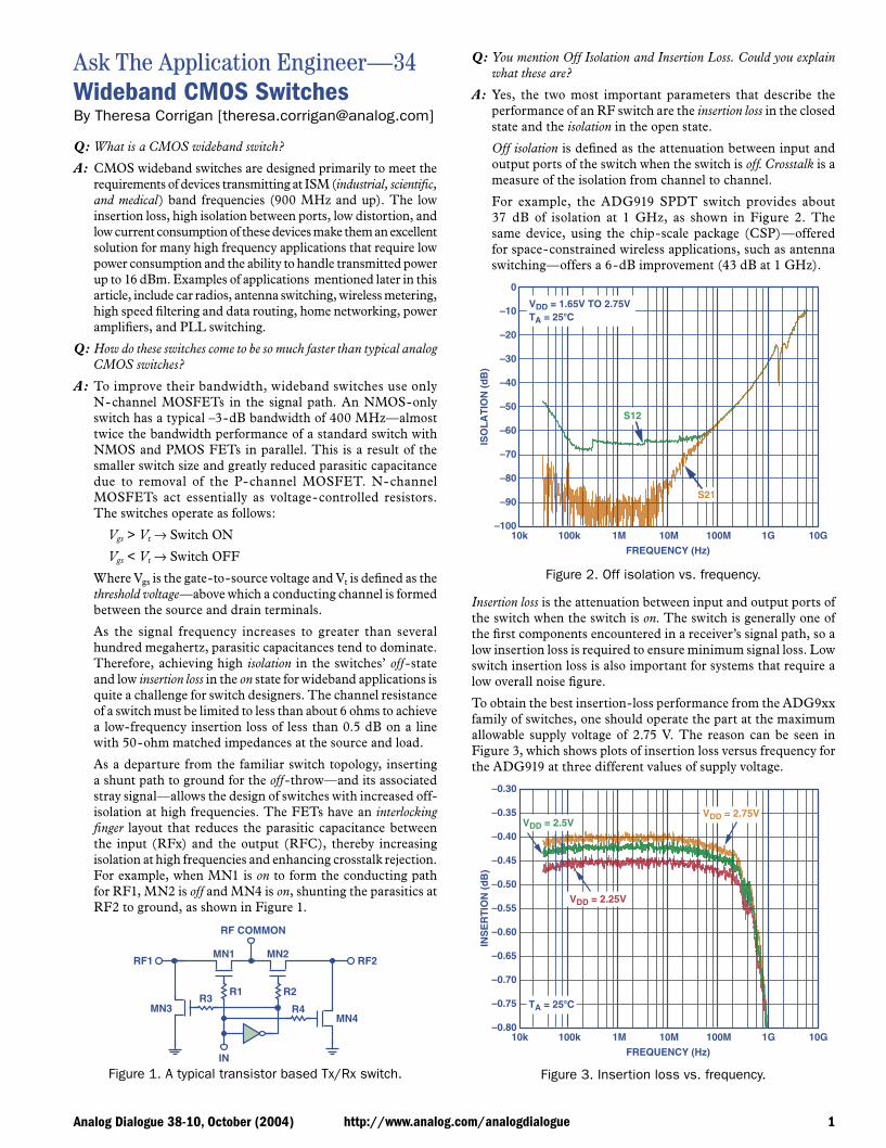
Analog Dialogue 38-10, October (2004) 1
Ask The Application Engineer—34Wideband CMOS SwitchesBy Theresa Corrigan [[email protected]]
Q: What is a CMOS wideband switch?
A: CMOS wideband switches are designed primarily to meet the requirements of devices transmitting at ISM (industrial, scientific, and medical) band frequencies (900 MHz and up). The low insertion loss, high isolation between ports, low distortion, and low current consumption of these devices make them an excellent solution for many high frequency applications that require low power consumption and the ability to handle transmitted power up to 16 dBm. Examples of applications mentioned later in this article, include car radios, antenna switching, wireless metering, high speed filtering and data routing, home networking, power amplifiers, and PLL switching.
Q: How do these switches come to be so much faster than typical analog CMOS switches?
A: To improve their bandwidth, wideband switches use only N-channel MOSFETs in the signal path. An NMOS-only switch has a typical –3-dB bandwidth of 400 MHz—almost twice the bandwidth performance of a standard switch with NMOS and PMOS FETs in parallel. This is a result of the smaller switch size and greatly reduced parasitic capacitance due to removal of the P-channel MOSFET. N-channel MOSFETs act essentially as voltage-controlled resistors. The switches operate as follows:
Vgs > Vt Æ Switch ON
Vgs < Vt Æ Switch OFF
Where Vgs is the gate-to-source voltage and Vt is defined as the threshold voltage—above which a conducting channel is formed between the source and drain terminals.
As the signal frequency increases to greater than several hundred megahertz, parasitic capacitances tend to dominate. Therefore, achieving high isolation in the switches’ off -state and low insertion loss in the on state for wideband applications is quite a challenge for switch designers. The channel resistance of a switch must be limited to less than about 6 ohms to achieve a low-frequency insertion loss of less than 0.5 dB on a line with 50-ohm matched impedances at the source and load.
As a departure from the familiar switch topology, inserting a shunt path to ground for the off -throw—and its associated stray signal—allows the design of switches with increased off-isolation at high frequencies. The FETs have an interlocking finger layout that reduces the parasitic capacitance between the input (RFx) and the output (RFC), thereby increasing isolation at high frequencies and enhancing crosstalk rejection. For example, when MN1 is on to form the conducting path for RF1, MN2 is off and MN4 is on, shunting the parasitics at RF2 to ground, as shown in Figure 1.
MN3MN4
R4R3
RF2RF1
RF COMMON
MN1
R1
MN2
R2
IN
Figure 1. A typical transistor based Tx/Rx switch.
Q: You mention Off Isolation and Insertion Loss. Could you explain what these are?
A: Yes, the two most important parameters that describe the performance of an RF switch are the insertion loss in the closed state and the isolation in the open state.
Off isolation is defined as the attenuation between input and output ports of the switch when the switch is off. Crosstalk is a measure of the isolation from channel to channel.
For example, the ADG919 SPDT switch provides about 37 dB of isolation at 1 GHz, as shown in Figure 2. The same device, using the chip-scale package (CSP)—offered for space-constrained wireless applications, such as antenna switching—offers a 6-dB improvement (43 dB at 1 GHz).
S12
S21
VDD = 1.65V TO 2.75V TA = 25C
–90
–70
–60
–50
–40
–30
–80
–20
–10
0
–10010k 100k 1M 10M 100M 1G 10G
ISO
LA
TIO
N (
dB
)
FREQUENCY (Hz)
Figure 2. Off isolation vs. frequency.
Insertion loss is the attenuation between input and output ports of the switch when the switch is on. The switch is generally one of the first components encountered in a receiver’s signal path, so a low insertion loss is required to ensure minimum signal loss. Low switch insertion loss is also important for systems that require a low overall noise figure.
To obtain the best insertion-loss performance from the ADG9xx family of switches, one should operate the part at the maximum allowable supply voltage of 2.75 V. The reason can be seen in Figure 3, which shows plots of insertion loss versus frequency for the ADG919 at three different values of supply voltage.
TA = 25C
VDD = 2.75VVDD = 2.5V
VDD = 2.25V
–0.30
–0.35
–0.40
–0.45
–0.50
–0.55
–0.60
–0.65
–0.70
–0.75
–0.8010k 100k 1M 10M 100M 1G 10G
INS
ER
TIO
N (
dB
)
FREQUENCY (Hz)
Figure 3. Insertion loss vs. frequency.
http://www.analog.com/analogdialogue

2 Analog Dialogue 38-10, October (2004)
Q: How does insertion loss relate to the On-resistance spec of a standard analog switch?
A: Signal loss is essentially determined by the attenuation introduced by switch resistance in the on condition, Ron, in series with the source-plus-load resistance—measured at the lower frequencies of operation. Figure 4 shows a typical profile of on -resistance as a function of source voltage for an N-channel MOSFET device.
28
24
20
16
12
8
40 0.4 0.8 1.2 1.6 2.0 2.4
RO
N (
)
VS (V)
Figure 4. On resistance vs. source voltage.
Q: What technologies have been commonly used in the design of high-frequency switches?
A: Traditionally, only a few processes were available for developing good wideband/RF switches. Gallium arsenide (GaAs) FETs, PIN diodes, and electromechanical relays have dominated the market, but standard CMOS is now a strong entry.
PIN diodes are highly linear devices with good distortion characteristics, but they have many drawbacks given today’s high performance demands. They have very slow switching times (microseconds, compared to nanoseconds for CMOS switches); they are power-hungry, making them unsuitable for many battery-operated devices; and—unlike CMOS switches with their response from RF to dc—there is a practical lower frequency limit to the use of PIN diodes as linear switches.
GaAs has been popular because of its low on resistance, low off capacitance, and high linearity at high frequencies. As CMOS process geometries continue to shrink, however, the performance of CMOS switches has increased to the extent that they can achieve –3-dB frequencies of up to 4 GHz and are able to compete with GaAs switches. Designed to maximize bandwidth while maintaining high linearity and low power consumption, CMOS switches now offer a practical alternative to GaAs switches in many low-power applications.
Q: So what are the main benefits of CMOS wideband switch solutions over gallium arsenide?
A: Switches, such as the ADG9xx family of parts, have an integrated TTL driver that allows easy interfacing with other CMOS devices, since CMOS is compatible with LVTTL logic levels. The small size of devices with integrated drivers is a solution for many space-constrained applications.
GaAs switches, as such, need dc-blocking capacitors in series with the RF ports, effectively floating the die relative to dc ground, so that the switches can be controlled with positive control voltages. Wideband switches, such as the ADG9xx family, do not have this requirement, eliminating concerns of reduced bandwidth, the impact of the capacitors on overall system performance, and the extra space and cost of GaAs solutions. Eliminating the blocking capacitors allows the ADG9xx parts to maintain their
low insertion loss (0.5 dB) all the way down to dc. In addition to providing a smaller, more efficient design solution, the ADG9xx family is less power-demanding, consuming less than 1 A over all voltage and temperature conditions.
Q: How about the ESD (electrostatic discharge) performance as compared to GaAs?
A: The ADG9xx family of parts passes the 1-kV ESD HBM (human body model) requirement. ESD protection circuitry is easily integrated on these CMOS devices to protect the RF and digital pins. This makes the switches ideal for any applications that are ESD sensitive, and they offer a reliable alternative to GaAs devices having ESD ratings as low as 200 V.
Q: What are the other important specifications of these switches?
A: Video Feedthrough (Figure 5) is the spurious dc transient present at the RF ports of the switch when the control voltage is switched from high- to- low-, or low- to- high, without an RF signal present. This is analogous to charge injection of a typical analog switch. It is measured in a 50-ohm test setup, with 1-ns (rise-time) pulses and a 500-MHz bandwidth.
CH1 500mV CH2 1mV M10.0ns
1
2
CH2 p-p2.002mV
T
CTRL
RFC
Figure 5. Video feedthrough.
P1dB (1-dB compression point) is the RF input power level at which the switch insertion loss increases by 1 dB over its low-level value. It is a measure of the RF power-handling capability of the switch. As shown in Figure 6, the ADG918 has a P1dB of 17 dBm at 1 GHz, with VDD = 2.5 V.
Q: What does this mean?
A: It means that if the insertion loss at 1 GHz was 0.8 dB with a low-level input, it would be 1.8 dB with a 17-dBm input signal [Note: dBm is the dB (logarithmic) measure of the ratio of power to 1 mW, or voltage to 224 mV in 50 ohms. 17 dBm corresponds to 50 mW, or 1.6 V rms or 4.5 V p-p].
20
0
2
4
6
8
10
12
14
16
18
0 250 500 750 1000 1250 1500
P–1
dB
(d
Bm
)
FREQUENCY (MHz)
VDD = 2.5V TA = 25C
Figure 6. 1-dB compression point vs. frequency.

Analog Dialogue 38-10, October (2004) 3
Q: Power-handling capability seems to decrease substantially at the lowest frequencies in Figure 6. Why?
A: In normal operation, the switches can handle a 7-dBm (5-mW) input signal. For a 50-ohm load, this corresponds to a 0.5-V rms signal, or 1.4 V peak-to-peak for sine waves. [V p-p = Vrms 2 ÷2].
The power handling capability is reduced at lower frequencies for two reasons:
VG
P TYPESUBSTRATE
50
VDVS50
N+N+
Figure 7. Physical NMOS structure.
As shown in Figure 7, the inherent NMOS structure consists of two regions of N-type material in a P-type substrate. Parasitic diodes are thus formed between the N and P regions. When an ac signal, biased at 0 V dc, is applied to the source of the transistor, and Vgs is large enough to turn the transistor on (Vgs > Vt), the parasitic diodes can be forward-biased for some portion of the negative half-cycle of the input waveform. This happens if the input sine wave goes below approximately –0.6 V, and the diode begins to turn on, thereby causing the input signal to be clipped (compressed), as shown in Figure 8. The plot shows a 100-MHz, 10-dBm input signal and the corresponding 100-MHz output signal. It is readily seen that the output signal has been truncated.
T
CH1 500mV M2.00ns
REF1 FREQ99.98MHzREF1 AMPL1.85V
C1 FREQ100.05MHzC1 AMPL1.51V
CH1 0V
Figure 8. 100-MHz, 10-dBm input/output signals with 0-V dc bias.
At low frequencies, the input signal is below the –0.6 V level for longer periods of time, and this has a greater impact on the 1-dB compression point (P1dB).
The second reason why parts can handle less power at lower frequencies is the partial turn-on of the shunt NMOS device when it is supposed to be off. This is very similar to the mechanism described above where there was partial turn-on of the parasitic diode. In this case, the NMOS transistor is in the off state, with Vgs < Vt. With an ac signal on the source of the shunt device, there will be a time in the negative half-cycle of the waveform where Vgs > Vt, thereby partially turning on the shunt device. This will compress the input waveform by shunting some of its energy to ground.
Both of the above mechanisms can be overcome by applying a small dc bias (about 0.5 V) to the RF input signal when the switch is being used at low frequencies (<30 MHz) and high power—greater than 7 dBm (or 5 mW, 1.4 V p-p in 50 ohms). This will raise the minimum level of the sine-wave input signal and thus ensure that the parasitic diodes are continually reverse-biased and that the shunt transistor, never seeing Vgs > Vt, remains in the off state for the whole period of the input signal. Figure 9 again shows a plot of input- and output signals at 100 MHz and 10 dBm input power (about 2 V p-p in 50 ohms), but this time with a 0.5-V dc bias. It is clearly visible that clipping or compression no longer occurs at 100 MHz.
T
CH1 500mV M2.00ns
REF1 FREQ99.98MHzREF1 AMPL1.85V
C1 FREQ100.00MHzC1 AMPL1.75V
CH1 0V
Figure 9. 100-MHz, 10-dBm input/output signals with 0.5-V dc bias.
Q: How do I apply a dc bias to RF inputs?
A: To minimize any current drain through the termination resistance on the input side, it is best to add the bias on the output (RFC) side. This is the best practice, especially for low-power portable applications, but it may be necessary to apply dc-blocking capacitors on the RF outputs if downstream circuitry cannot handle the dc bias.
Q: Can these switches operate with a negative supply?
A: They can operate with a negative signal on the GND (ground) pin as long as it adheres to the –0.5 V to +4 V Absolute Maximum Rating for VDD to GND. Note that operating the part in this manner places the internal terminations at this new GND potential—an undesirable effect in some applications.
Q: What about the distortion performance of these switches?
A: When tones at closely spaced frequencies are passed through a switch, the nonlinearity of the switch causes false tones to be generated, causing undesired outputs at other frequencies. In communications systems, where channels are becoming more tightly spaced, it is essential to minimize this intermodulation distortion (IMD) to ensure minimum interference. Applying two closely spaced equal-power signals with a set frequency spacing (e.g., 900 MHz and 901 MHz) to the input of a device under test (DUT), results in the output spectrum shown in Figure 10. The 3rd-order harmonic, usually expressed in dBc, is the log of the ratio of the power in the 3rd order harmonic to the power of the fundamental. The larger the (negative) value, the lower the distortion. Sending these tones through the ADG918, using a combiner with an input power of 4 dBm, resulted in an IP3 of 35 dBm as shown in Figure 11. [Note: an excellent discussion of various types of distortion can be found in “Ask The Applications Engineer—13”]1
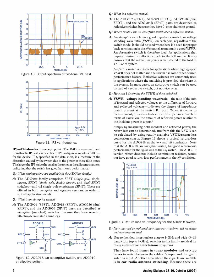
4 Analog Dialogue 38-10, October (2004)
0
–50
–45
–40
–35
–30
–25
–20
–15
–10
–5
f12f1 f2 2f2 f1f2
INT
ER
MO
DU
LA
TIO
N D
IST
OR
TIO
N (
dB
)
FREQUENCY
IMDPRODUCT
FUNDAMENTAL
Figure 10. Output spectrum of two-tone IMD test.
40
35
30
25
20
15
10
5
0250 350 450 550 650 750 850
IP3
(dB
m)
FREQUENCY (MHz)
VDD = 2.5V TA = 25C
Figure 11. IP3 vs. frequency.
IP3—Third-order intercept point. The IMD is measured, and from this the IP3 value is calculated. IP3 is a figure of merit—in dBm—for the device. IP3, specified in the data sheet, is a measure of the distortion caused by the switch due to the power in these false tones. The larger the IP3 value the smaller the tones in the adjacent channels, indicating that the switch has good harmonic performance.
Q: What configurations are available in the ADG9xx family?
A: The ADG9xx family comprises SPST (single-pole, single-throw), SPDT (single-pole, double-throw), and dual -SPDT switches—and 4:1 single-pole multiplexers (SP4T). These are offered in both absorptive and reflective versions, in order to suit all application needs.
Q: What is an absorptive switch?
A: The ADG901 (SPST), ADG918 (SPDT), ADG936 (dual SPDT), and the ADG904 (SP4T) parts are described as absorptive (matched) switches, because they have on-chip 50-ohm-terminated shunt legs.
RF2
RF1
CTRL
ADG918
RFC 50
50
ADG919
RF2
RF1
CTRL
RFC
Figure 12. ADG918, an absorptive switch, and ADG919, a reflective switch.
Q: What is a reflective switch?
A: The ADG902 (SPST), ADG919 (SPDT), ADG936R (dual SPDT), and the ADG904R (SP4T) parts are described as reflective switches because they have 0-ohm shunts to ground.
Q: Where would I use an absorptive switch over a reflective switch?
A: An absorptive switch has a good impedance-match, or voltage standing-wave ratio (VSWR), on each port, regardless of the switch mode. It should be used when there is a need for proper back-termination in the off channel, to maintain a good VSWR. An absorptive switch is therefore ideal for applications that require minimum reflections back to the RF source. It also ensures that the maximum power is transferred to the load in a 50-ohm system.
A reflective switch is suitable for applications where high off -port VSWR does not matter and the switch has some other desired performance feature. Reflective switches are commonly used in applications where the matching is provided elsewhere in the system. In most cases, an absorptive switch can be used instead of a reflective switch, but not vice versa.
Q: How can I determine the VSWR of these switches?
A: VSWR—voltage standing-wave ratio—the ratio of the sum of forward and reflected voltages to the difference of forward and reflected voltages—indicates the degree of impedance match present at the switch RF port. When it comes to measurement, it is easier to describe the impedance match in terms of return loss, the amount of reflected power relative to the incident power at a port.2
Simply by measuring both incident and reflected power, the return loss can be determined, and from this the VSWR can be calculated by using readily available VSWR/return-loss conversion charts. Figure 13 shows a typical return-loss curve for the ADG918 in the on - and off conditions. Note that the ADG918, an absorptive switch, has good return-loss performance for the off, as well as the on, switch. The ADG919 version, which does not include termination resistors, would not have good return-loss performance in the off condition.
0
–5
–10
–15
–20
–25
–30
–35
–4010k 100k 1M 10M 100M 1G 10G
RE
TU
RN
LO
SS
(d
B)
FREQUENCY (Hz)
OFF SWITCH (ADG918)
ON SWITCH
TA = 25CVDD = 2.5V
Figure 13. Return loss vs. frequency for the ADG918 switch.
Q: Now that you’ve explained how these parts perform, tell me where and how they are used.
A: Due to their low insertion loss at up to 1-GHz and wide –3-dB bandwidth (up to 4 GHz), switches in this family are ideal for many automotive entertainment systems.
They have found homes in tuner modules and set-top boxes to switch between the cable-TV input and the off-air antenna input. Another area where these parts are suitable is in car-radio antenna switching. Because these are

Analog Dialogue 38-10, October (2004) 5
generally 50-ohm-impedance systems, the 50-ohm internal terminations offered by the absorptive version of these switches—the ADG901, ADG918, and ADG904—ensure excellent impedance-matching and minimum reflections.
The variety of topologies available makes these parts very easy to design into antenna-diversity-switch applications, allowing the user to switch between several antennas and a single tuner in multiband radios.
These parts are also suitable for wireless metering systems, providing the required isolation between transmit and receive signals (Figure 14).
LNAANTENNA
Tx/Rx SWITCH PA
ADG918
Figure 14. Tx/Rx Switching.
These parts are perfect for high-speed filter selection and data routing: the ADG904 can be used as a 4:1 demultiplexer to switch high-frequency signals between different filters—and also to multiplex the signal to the output. For differential filter selection and data routing, the ADG936 dual SPDT (single-pole, double- throw) switch is an ideal solution. Data switching in modem cards for point-to-point wireless systems, such as microwave radio links for military and avionic applications, requires the high-frequency performance offered by the ADG9xx family of parts.
They are also suitable for home-networking applications—systems allowing the wireless remote control of many different functions, such as opening and closing roller blinds, control of lighting (on, off or dimming)—in which the information is transmitted through a wireless link. The excellent isolation performance at high frequency and low power-consumption preserve a system’s current budget—thus constituting an ideal application.
Due to their high frequency range—up to 4 GHz—this family of parts are also suitable for many Bluetooth technologies—enabling wireless communication in the 2.5 -GHz ISM frequency band.
Wideband switches can be used in the design of power amplif iers (PAs) with 800 -, 900 -, 1900 -, 2100 -MHz frequencies—for cellular CDMA and GSM applications. The switch is used in the feed forward correction loop around the main amplif ier, allowing the active - and passive feedback- and feed-forward paths to be switched out, permitting the amplif ier’s distortion levels to be tested. The switch allows for gain- and phase correction in the system. The high isolation, low insertion loss, and the low distortion at 900 MHz make the ADG9xx family ideal for PA design in this frequency range.
The ADG918 can be used to implement PLL switching for frequency-hopping in GSM applications.
Q: What is PLL Switching, and why use the ADG918?
A: Switching between two phase-locked loops (PLLs)—commonly described as the ping-pong technique—allows a designer to achieve faster system settling times. The low power-consumption and simple single-pin control of the ADG918 make it an easy solution to integrate.
In switching between two oscillators, the desired isolation performance can be achieved by cascading—i.e., connecting a number of switches in cascade. This is a very simple way to provide a high-isolation specification for a system, preventing any interference at the higher frequencies. Cascading five ADG918s provides 130-dB isolation at 1 GHz, with an insertion loss of 3 dB. In this application, such an increase in insertion loss is not material, since the principal concern is about the signal levels relative to one another.
A nice feature of the ADG918 in this application is that it acts as an integrated low-pass filter, eliminating the unwanted harmonics created by the two PLLs. Achieved by the natural increase in insertion loss at high frequencies, it easily prevents the unwanted harmonics from propagating through the switches, as shown in Figures 15 and 16.
PLL 1
PLL 2
SWITCHO/P
Figure 15. PLL switching application.
ADG9xx
f 2f 3f
GaAs SWITCH
Figure 16. ADG918 switch cascade acting as integrated low-pass filter, compared with naked GaAs switching.
Q: So...to summarize?
A: In summary, CMOS wideband switches, especially those in the ADG9xx family, are excellent choices for all applications in the ISM band that require high isolation and low insertion-loss for battery-operated devices with space constraints. Evaluation kits are available from Analog Devices to make the design-in of these parts fast and hassle free—every designer’s dream! b
NOTES1http://www.analog.com/library/analogDialogue/Anniversary/13.html2https://ewhdbks.mugu.navy.mil/VSWR.htm

Analog Dialogue 40-10, October (2006) 1
Ask The Application Engineer—35Capacitance Sensors for Human Interfaces to Electronic EquipmentBy Susan Pratt [[email protected]]Q:What is a capacitance sensor?
A: Capacitance sensors detect a change in capacitance when something or someone approaches or touches the sensor. The technique has been used in industrial applications for many years to measure liquid levels, humidity, and material composition. A newer application, coming into widespread use, is in human-to-machine interfaces. Mechanical buttons, switches, and jog wheels have long been used as the interface between the user and the machine. Because of their many drawbacks, however, interface designers have been increasingly looking for more reliable solutions. Capacitive sensors can be used in the same manner as buttons, but they also can function with greater versatility, for example, when implementing a 128-position scroll bar.
Integrated circuits specifically designed to implement capacitance sensing in human-machine interface applications are now available from Analog Devices. The AD71421 and the AD7143, for example, can stimulate and respond to up to 14 and eight capacitance sensors, respectively. They provide excitation to the capacitance sensor, sense the changes in capacitance caused by the user’s proximity, and provide a digital output.
Q:How does capacitance sensing work?
A: A basic sensor includes a receiver and a transmitter, each of which consists of metal traces formed on layers of a printed-circuit board (PCB). As shown in Figure 1, the AD714x has an on-chip excitation source, which is connected to the transmitter trace of the sensor. Between the receiver and the transmitter trace, an electric field is formed. Most of the field is concentrated between the two layers of the sensor PCB. However, a fringe electric field extends from the transmitter, out of the PCB, and terminates back at the receiver. The field strength at the receiver is measured by the on-chip sigma-delta capacitance-to-digital converter. The electrical environment changes when a human hand invades the fringe field, with a portion of the electric field being shunted to ground instead of terminating at the receiver. The resultant decrease in capacitance—on the order of femtofarads as compared to picofarads for the bulk of the electric field—is detected by the converter.
EXCITATIONSIGNAL250kHz
-ADC
16-BITDATA
CAPACITANCE-TO-DIGITAL CONVERTER
Tx
Rx
PLASTIC COVER
USER INTERFERESWITH FRINGE FIELD
BULK OF FIELDCONFINEDBETWEENTx AND Rx
Figure 1. Sensing capacitance.
http://www.analog.com/analogdialogue
In general, there are three parts to the capacitance-sensing solution, all of which can be supplied by Analog Devices.
• The driver IC, which provides the excitation, the capacitance-to-digital converter, and compensation circuitry to ensure accurate results in all environments.
• The sensor—a PCB with a pattern of traces, such as buttons, scroll bars, scroll wheels, or some combination. The traces can be copper, carbon, or silver, while the PCB can be FR4, flex, PET, or ITO.
• Software on the host microcontroller to implement the serial interface and the device setup, as well as the interrupt service routine. For high-resolution sensors such as scroll bars and wheels, the host runs a software algorithm to achieve high resolution output. No software is required for buttons.
AD7142/AD7143
SENSORS
EXCITATION SOURCE
SERIAL INTERFACE4-WIRE SPI® (AD7142 ONLY)
2-WIRE I2C® (AD7142 AND AD7143)
14 OR 8
INTERRUPTCIN
HOST SOFTWARE:- SERIAL INTERFACE- CODE TO SUPPORT POSITIONING
HOSTP
CIRCUIT BOARD
Figure 2. Three-part capacitance-sensing solution.
Q:What are the advantages of capacitive sensing?
A: Capacitance sensors are more reliable than mechanical sensors—for a number of reasons. There are no moving parts, so there is no wear and tear on the sensor, which is protected by covering material, for example, the plastic cover of an MP3 player. Humans are never in direct contact with the sensor, so it can be sealed away from dirt or spillages. This makes capacitance sensors especially suitable for devices that need to be cleaned regularly—as the sensor will not be damaged by harsh abrasive cleaning agents—and for hand-held devices, where the likelihood of accidental spillages (e.g., coffee) is not negligible.
Q:Tell me more about how the AD714x ICs work.
A: These capacitance-to-digital converters are designed specif ically for capacitance sensing in human-interface applications. The core of the devices is a 16-bit sigma-delta capacitance-to-digital converter (CDC), which converts the capacitive input signals (routed by a switch matrix) into digital values. The result of the conversion is stored in on-chip registers. The on-chip excitation source is a 250-kHz square wave.
The host reads the results over the serial interface. The AD7142, available with either SPI®- or I2C®-compatible interfaces, has 14 capacitance-input pins. The AD7143, with its I2C interface, has eight capacitance-input pins. The serial interface, along with an interrupt output, allows the devices to connect easily to the host microcontroller in any system.

2 Analog Dialogue 40-10, October (2006)
TESTVREF+VREF–
INT
CSHIELD
SRC
SRC
SW
ITC
HM
AT
RIX
CONTROLAND DATA
REGISTERS
CALIBRATIONRAM
250kHzEXCITATION
SOURCE
INTERRUPTAND GPIO
LOGIC
POWER-ONRESETLOGIC
AVCC
AGND
DGND1
DGND2
DVCC
GPIO
19
18
17
14
13
272829
CIN0 30
CIN1 31
CIN2 32
CIN3 1
CIN4 2
CIN5 3
CIN6 4
CIN7 5
CIN8 6
CIN9 7
CIN10 8
CIN11 9
CIN12 10
CIN13 11
12
15
16
25
26VDRIVE 20
SDO/SDA
SDI/ADD0
SCLK CS/ADD1
SERIAL INTERFACEAND CONTROL LOGIC
21 22 23 24
16-BIT-
CDC
CALIBRATIONENGINE
Figure 3. AD7142 block diagram.
These devices interface with up to 14 external capacitance sensors, arranged as buttons, bars, wheels, or a combination of sensor types. The external sensors consist of electrodes on a 2- or 4-layer PCB that interfaces directly with the IC.
The devices can be set up to interface with any set of input sensors by programming the on-chip registers. The registers can also be programmed to control features such as averaging and offset adjustment for each of the external sensors. An on-chip sequencer controls how each of the capacitance inputs is polled.
The AD714x also include on-chip digital logic and 528 words of RAM that are used for environmental compensation. Humidity, temperature, and other environmental factors can af fect the operation of capacitance sensors ; so, transparently to the user, the devices perform continuous calibration to compensate for these effects, giving error-free results at all times.
One of the key features of the AD714x is sensitivity control, which imparts a different sensitivity setting to each sensor, controlling how soft or hard the user’s touch must be to activate the sensor. These independent settings for activation thresholds, which determine when a sensor is active, are vital when considering the operation of different-size sensors. Take, for example, an application that has a large, 10-mm-diameter button, and a small, 5-mm-diameter button. The user expects both to activate with same touch pressure, but capacitance is related to sensor area, so a smaller sensor needs a harder touch to activate it. The end user should not have to press one button harder than another for the same effect, so having independent sensitivity settings for each sensor solves this problem.
Q:How is the environment taken into account?
A: The AD714x measures the capacitance level from the sensor continuously. When the sensor is not active, the capacitance value measured is stored as the ambient value. When a user comes close to or touches the capacitance sensor, the measured capacitance decreases or increases. Threshold capacitance levels are stored in on-chip registers. When the measured capacitance value exceeds either upper or lower threshold limits, the sensor is considered to be active—as shown in Figure 4—and an interrupt output is asserted.
THRESHOLD
THRESHOLD
SENSORTOUCH
AMBIENT CAPACITANCE VALUE
CD
C O
UT
PU
T C
OD
E
65536
0SENSORTOUCH
Figure 4. Sensor activation.
Figure 4 shows an ideal situation, where the ambient capacitance value does not change. In reality, the ambient capacitance changes constantly and unpredictably due to changes in temperature and humidity. If the ambient capacitance value changes sufficiently, it can affect the sensor activation. In Figure 5, the ambient capacitance value increases; Sensor 1 activates correctly, but when the user tries to activate Sensor 2, an error occurs. The ambient value has increased, so the change in capacitance measured from Sensor 2 is not large enough to bring the value below the lower threshold. Sensor 2 cannot now be activated, no matter what the user does, as its capacitance cannot decrease below the lower threshold in these circumstances. A worse possibility is that the ambient capacitance level continues to increase until it is above the upper threshold. In this case, Sensor 1 will become active, even though the user has not activated it, and it will remain active—the sensor will be “stuck” on—until the ambient capacitance falls.
CD
C O
UT
PU
T C
OD
ES
t
SENSOR 1 INTASSERTED
CHANGING ENVIRONMENTAL CONDITIONS
SENSOR 2 INTNOT ASSERTED
Figure 5. Sensor activation with changing ambient capacitance.
On-chip logic circuits deal with the effects of changing ambient capacitance levels. As Figure 6 shows, the threshold levels are not constant; they track any changes in the ambient capacitance level, maintaining a fixed distance away from the ambient level to ensure that the change in capacitance due to user activation is always sufficient to exceed the threshold levels. The threshold levels are adapted automatically by the on-chip logic and are stored in the on-chip RAM. No input from the user or host processor is required.
CD
C O
UT
PU
T C
OD
ES
t
SENSOR 1 INTASSERTED
1
4
2
5
3
6
CHANGING ENVIRONMENTAL CONDITIONS
SENSOR 2 INTNOT ASSERTED
Figure 6. Sensor activation with auto-adapting thresholds.

Analog Dialogue 40-10, October (2006)
Q:How is capacitance sensing applied?
A: As noted earlier, the sensor traces can be any number of different shapes and sizes. Buttons, wheels, scroll-bar, joypad, and touchpad shapes can be laid out as traces on the sensor PCB. Figure 7 shows a selection of capacitance sensor layouts.
Sensor
But
ton
SRC
CIN SRC CIN
8-W
ay S
wit
ch
CINCIN
CIN
CIN
SRC
Sli
der
Whe
elK
eypa
dT
ouch
pad
Figure 7. Selection of capacitance sensors.
Many options for implementing the user interface are available to the designer, ranging from simply replacing mechanical buttons with capacitive button sensors to eliminating buttons by using a joypad with eight output positions, or a scroll wheel that gives 128 output positions.
The number of sensors that can be implemented using a single device depends on the type of sensors required. The AD7142 has 14 capacitance input pins and 12 conversion channels. The AD7143 has eight capacitance inputs and eight conversion channels. The table below shows the number of input pins and conversion stages required for each sensor type. Any number of sensors can be combined, up to the limit established by the number of available inputs and channels.
Sensor TypeNumber of CIN inputs required
Number of conversion channels required
Button 1 1 (0.5 for differential operation)
8-Way Switch
4—top, bottom, left, and right 3
Slider 8—1 per segment 8—1 per segment
Wheel 8—1 per segment 8—1 per segment
Keypad Touchpad
1 per row, 1 per column
1 per row, 1 per column
Measurements are taken on all connected sensors sequentially—in a “round-robin” fashion. All sensors can be measured within 36 ms, though, allowing essentially simultaneous detection of each sensor’s status—as it would take a very fast user to activate or deactivate a sensor within 40 ms.
Q:What design help can you offer first-time users?
A: Analog Devices has a number of resources available to designers of capacitance sensors. The first step in the design process is to decide what types of sensors are needed in the application. Will the user need to scan quickly through long lists, such as contacts on a handset or songs on an MP3 player? If so, then consider using a scroll bar or scroll wheel to allow the user to scan through those lists quickly and efficiently. Will the user need to control a cursor moving around a screen? An X-Y joypad would be a good fit for this application. Once the type, number, and dimensions of the required sensors have been fixed, the sensor PCB design can begin.
As part of the design resources available for capacitance sensing, a Mentor Graphics PADs layout library is available online. Many different types and sizes of sensors are available in this library as components, which can be dragged and dropped directly into a PCB layout. The library is available as an interactive part of the Touch Controller System Block Diagram.2 Also available is AN-854,3 an application note that provides details, tips, and tricks on how to use the sensor library to lay out the desired sensors quickly.
When designing the PCB, place the AD7142 or AD7143 on the same board as the sensors to minimize the chances of system errors due to moving connectors and changing capacitance. Other components, LEDs, connectors, and other ICs, for example, can go on the same PCB as the capacitance sensors, but the sensor PCB must be glued or taped to the covering material to prevent air gaps above the sensors, so the placement of any other components on the PCB must take this into account.
For applications where RF noise is a concern, then an RC filter can be used to minimize any interference with the sensors. Using a ground plane around the sensors will also minimize any interference.
The PCB can have either two- or four layers. A 4-layer design must be used when there is no room, outside of the sensor active areas, to route between the IC and the sensors, but a 2-layer design can be used if there is enough routing room.
4 Analog Dialogue 40-10, October (2006)
The maximum distance allowed between the sensor traces and capacitance input pin is 10 cm, but one sensor can be 10 cm from the pins in one direction, while another can be 10 cm from the pins in the opposite direction, allowing 20 cm between sensors.
Q:My sensor PCB is ready, now what?
A: Capacitance is notoriously difficult to simulate, so the sensor response in each application must be characterized to ensure that the AD7142/AD7143 is set up optimally for the application. This characterization process need only take place once per application, with the same setup values then being used for each individual product.
The sensors are characterized in the application. This means that any covering material must be in place on top of the sensor, and any other PCBs or components that may have an effect on the sensor’s performance must be in place around the sensor.
For each conversion channel, we need to configure:
• Internal connection from the device’s CIN input pin to the converter. This ensures that each sensor is connected to the converter using one conversion channel.
• Sensor offset value, to offset for CBULK. This is the capacitance associated with the electric field that is confined within the PCB, between the transmitter and receiver electrodes. This value does not change when the sensor is active, but instead provides a constant offset for the measurement fringe capacitance value.
• Initial values for upper and lower offset registers. These values are used by the on-chip logic to determine the activation threshold for each sensor.
The easiest way to perform the characterization is to connect the sensor PCB to the AD7142/AD7143 evaluation board—available from Analog Devices. The microcontroller and software that are included on the evaluation board can be used to characterize the sensor response and save the setup values.
Q:What kind of response can I expect?
A: The practical response from the sensor is defined by the converter’s output change when the sensor goes from inactive to active. This change will depend on the area of the sensor—the larger the sensor area, the greater the change when the sensor is active. The sensor response will also depend on the thickness of the covering material—if it is very thick (4 mm or more), the sensor response will be minimal. The reason is that the electric field will not penetrate through very thick covering material, so the user will not be able to shunt enough of the field to ground to generate a large response. Figure 8 is a typical sensor response from a button sensor. It shows a change of about 250 LSBs between the sensor active and sensor inactive in this case.
35100
35000
34900
34800
34700
SENSOR NOT ACTIVE
SENSOR ACTIVE
UPPERACTIVATIONTHRESHOLD
LOWERACTIVATIONTHRESHOLDMEASURED RESPONSE
FROM SENSOR
Figure 8. Typical response from a button sensor.
Q:You mentioned software?
A: The interaction between the host processor and the AD7142/AD7143 is interrupt-driven. The host implements the serial interface, either SPI or I2C. The AD7142/AD7143 will interrupt the host when a sensor is touched. The host can then read back data from the on-chip registers. If the sensors are buttons, or other simple on/off type sensors, the host simply reads back from the on-chip status registers; an active button causes a bit to be set in the status register. However, if the sensors have a high-resolution output, a software algorithm must run in the host interrupt routine to process the AD7142/AD7143 data.
The code is provided free of charge or royalties to customers who sign a license agreement with Analog Devices. For a scroll bar, the code typically occupies 500 bytes of data memory and 8k bytes of code memory. For a scroll wheel, the code typically occupies 600 bytes of data memory and 10k bytes of code memory.
Analog Devices provides sample drivers,4 written in C-code, for basic configuration, button sensors, and 8-way switches using SPI- and I2C-compatible interfaces. Sample drivers for scroll wheels and scroll bars are available after signing a software license.
Q:Ideas on assembling my finished product?
A: No air gap is allowed between the sensor PCB and the covering material or product case because having one would cause less of the electric field to extend above plastic, decreasing the sensor response. Also, the plastic or other covering material might bend on contact, causing the user to interact with a variable electric field, and resulting in a nonlinear sensor response. Thus, the sensor PCB should be glued to the covering material to prevent any air gaps from forming.
Also, there can be no floating metal around the sensors. A “Keep Out” distance of 5 cm is required. Metal closer to the sensors than 5 cm should be grounded, but there can be no metal closer to the sensors than 0.2 mm.
Finally, the plastic covering the sensor’s active areas should be about 2 mm thick. Larger sensor areas should be used with thicker plastic; and plastic thickness of up to 4 mm can be supported.
CONCLUSIONCapacitance sensors are an emerging technology for human-machine interfaces and are rapidly becoming the preferred technology over a range of different products and devices. Capacitance sensors enable innovative yet easy-to-use interfaces for a wide range of portable and consumer products. Easy to design, they use standard PCB manufacturing techniques and are more reliable than mechanical switches. They give the industrial designer freedom to focus on styling, knowing that capacitance sensors can be relied upon to give a high-performance interface that will fit the design. The designer can benefit from the Analog Devices portfolio of IC technology and products, plus the expertise and the hardware and software tools available to make it as easy and as quick as possible to design-in capacitance sensors. b
REFERENCES—VALID AS OF OCTOBER 20061 ADI website: www.analog.com (Search) AD7142 (Go)2ADI website: www.analog.com (Search) Touch Controller System Block Diagram (Go)
3 ADI website: www.analog.com (Search) AN-854 (Go)4 http:/ /www.analog.com/en/content/0,2886,760_1077_F107310,00.html#software

Analog Dialogue 41-02, February (2007) 1
Ask The Application Engineer—36Wideband A/D Converter Front-End Design Considerations II: Amplifier- or Transformer Drive for the ADC?
By Rob Reeder [[email protected]] Jim Caserta [[email protected]]
Design of the input configuration, or “front end,” ahead of a high-performance analog-to-digital converter (ADC) is critical to achieving desired system performance. Optimizing the overall design depends on many factors, including the nature of the application, system partition, and ADC architecture. The following questions and answers highlight the important practical considerations affecting the design of an ADC front end using amplifier- and transformer circuitry.
Q. What is the fundamental difference between amplifiers and transformers?
A. An amplifier is an active element, while a transformer is passive. Amplifiers, like all active elements, consume power and add noise; transformers consume no power and add negligible noise. Both have dynamic effects to be dealt with.
Q. Why would you use an amplifier?
A. Amplifier performance has fewer limitations than those of transformers. If dc levels must be preserved, an amplifier must be used, because transformers are inherently ac-coupled devices. On the other hand, transformers provide galvanic isolation if needed. Amplifiers provide gain more easily because their output impedance is essentially independent of gain. On the other hand, a transformer’s output impedance increases with the square of the voltage gain—which depends on the turns ratio. Amplifiers provide flatter response in the pass band, free of the ripple due to the parasitic interactions in transformers.
Q. How much noise does an amplifier typically add, and what can I do to reduce this?
A. A typical amplifier that might be considered, the ADA4937,1 for example, when configured for G = 1, has an output noise spectral density of 6 nV/√Hz at high frequencies, compared to the 10-nV/√Hz input noise spectral density of the 80-MSPS AD9446-802 ADC. The problem here is that the amplifier has a noise bandwidth equivalent to the full bandwidth of the ADC, around 500 MHz, while the ADC noise is folded to one Nyquist zone (40 MHz). Without a filter, the integrated noise then becomes 155 mV rms for the amplifier and 90 mV rms for the ADC. Theoretically, this degrades the overall system SNR (signal-to-noise ratio) by 6 dB. To confirm this experimentally, the measured SNR, with the ADA4937 driving the AD9446-80, is 76 dBFS, and the noise floor is –118 dB (Figure 1). With a transformer drive, the SNR is 82 dBFS. The driver amplifier has thus degraded the SNR by 6 dB.
http://www.analog.com/analogdialogue
0
–150
–140
–130
–120
–110
–100
–90
–80
–70
–60
–50
–40
–30
–20
–10
0 4 8 12 16 20 24 28 32 36 40
AM
PL
ITU
DE
(d
BF
S)
FREQUENCY (MHz)
4
+ 5
1
6
2
ENCODE: 80MHzSAMPLES: 32768ANALOG: 19.0991MHz
FUND: –0.997dBFS2ND: –86.5dBc3RD: –83.03dBc4TH: –103.38dBc5TH: –100.03dBc6TH: –95.59dBc
SNR: 74.81dBcSNRFS: 75.8dBFSTHD: –81.17dBcSINAD: 73.9dBcSFDR: 82.64dBcWO SPUR: –98.31dBcNOISE FLOOR: –117.9dB
FUND LEAD: 100HARM LEAK: 3DC LEAK: 6
3
Figure 1. ADA4937 amplifier driving an AD9446-80 ADC at 80 MSPS without a noise filter.
To make better use of the ADC’s SNR, a filter is inserted between the amplifier and ADC. With a 100-MHz 2-pole filter, the amplifier’s integrated noise becomes 71 mV rms, degrading the ADC’s SNR by only 3 dB. Use of the 2-pole filter improves the SNR performance of the Figure 1 circuit to 79 dBFS, with a noise floor of –121 dB, as shown in Figure 2a. The 2-pole filter is built with 24-V resistors and 30-nH inductors in series with each of the amplifier’s outputs, and a 47-pF differentially connected capacitor (Figure 2b).
0
–150
–140
–130
–120
–110
–100
–90
–80
–70
–60
–50
–40
–30
–20
–10
0 4 8 12 16 20 24 28 32 36 40
AM
PL
ITU
DE
(d
BF
S)
FREQUENCY (MHz)
5
1
6
ENCODE: 80MHzSAMPLES: 32768ANALOG: 19.0991MHz
FUND: –1.036dBFS2ND: –82.97dBc3RD: –82.94dBc4TH: –102.95dBc5TH: –98.1dBc6TH: –96.3dBc
SNR: 78.11dBcSNRFS: 79.14dBFSTHD: –79.76dBcSINAD: 75.85dBcSFDR: 82.56dBcWO SPUR: –100.61dBcNOISE FLOOR: –121.3dB
FUND LEAD: 100HARM LEAK: 3DC LEAK: 6
3
4
2
+
Figure 2a. Driving an AD9446-80 with a 100-MHz noise filter.
30nH
30nH
47pF
24
AVDD
3pF2k
24
ADA4937AV = UNITY
ADC INPUTIMPEDANCE
AD9446
VOCM
200
18k
10k
200
200
228
0.1 F
50
SIGNALGENERATOR
Figure 2b. Schematic diagram of ADA4937 amplifier driving an AD9446-80 ADC at 80 MSPS with a 2-pole noise filter.

2 Analog Dialogue 41-02, February (2007)
Q. How do high-speed amplifiers and ADCs compare in power consumption?
A. This depends on the amplifier and ADC used. Two typical amplifiers, with similar power consumption, are the AD8352,3 which draws 37 mA @ 5 V (185 mW), and the ADA4937, which draws 40 mA @ 5 V (200 mW). Overall power consumption can be reduced by about one-third, with slightly degraded performance, by using a 3.3-V supply. ADCs feature more diversity in power consumption, depending on resolution and speed. The 16-bit, 80-MSPS AD9446-80 draws 2.4 W, the 14-bit, 125-MSPS AD9246-1254 draws 415 mW, and the 12-bit, 20-MSPS AD9235-205 draws only 95 mW.
Q. When do you need to use a transformer?
A. Transformers offer the biggest performance advantage compared to amplifiers at very high signal frequencies and when significant additional noise cannot be tolerated at the ADC input.
Q. How do transformers and amplifiers differ when providing gain?
A. The main difference is in the impedance they present to the ADC input, which directly affects system bandwidth. A transformer’s input- and output impedance are related by the square of the turns ratio, while an amplifier’s input and output impedance are essentially independent of gain.
For example, when a G = 2 transformer is used from a 50-V source impedance, the impedance seen at the secondary side of the transformer is 200 V. The AD9246 ADC has a differential input capacitance of 4 pF which, coupled with the 200-V transformer impedance, reduces the ADC’s –3-dB bandwidth from 650 MHz to 200 MHz. Extra series resistance and differential capacitance are often needed to improve performance and reduce kickback from the converter, which can limit –3-dB bandwidth further, possibly to 100 MHz.
When a low-output-impedance amplif ier—such as the ADA4937—is used, the result is a very low source impedance, usually less than 5 V. 25-V transient-limiting resistors can be used in series with each ADC input; in the case of the AD9246, the ADC’s full 650-MHz analog input bandwidth would be usable.
So far the discussion has been about –3-dB bandwidths. When tighter flatness is needed, say 0.5 dB in a 1-pole system, the −3-dB bandwidth needs to be about 33 wider. For 0.1-dB flatness with one pole, the ratio increases to 6.53. If 0.5-dB flatness is required at up to 150 MHz, a –3-dB bandwidth greater than 450 MHz is required, which is difficult to attain with a G = 2 transformer but is straightforward with a low-output-impedance amplifier.
Q. What are the factors to consider in choosing a transformer or an amplifier to drive an ADC?
A. They can be boiled down to a half-dozen parameters—outlined in this table:
Parameter Usualpreference Bandwidth Transformer Gain Amplifier Pass band flatness Amplifier Power requirement Transformer Noise Transformer DC vs. ac coupling Amplifier (dc level preservation)
Transformer (dc isolation)
Applications in which key parameters are in conflict require additional analysis and trade-offs.
Q. What are some considerations in this analysis?
A. One must start by understanding the level of difficulty in designing a front end for a given ADC. First, is the ADC internally buffered, or is it unbuffered (for example, a switched-capacitor type)? Naturally, the level of difficulty increases as the frequency increases in either case. But switched-capacitor types are more difficult for the designer to deal with.
If gain is needed to make full use of the ADC’s input range, an application that might otherwise favor a transformer becomes more difficult as the required gain (turns ratio) increases.
Of course, the difficulty increases with frequency. Design of an IF system below 100 MHz with a buffered ADC would be relatively simple compared to a high-IF design with low signal levels using an unbuffered ADC, as Figure 3 illustrates. With so many parameters pulling in different directions, trade-offs are sometimes difficult and often puzzling to keep track of as components are changed and evaluated.
BASEBAND
UNBUFFEREDADCs
BUFFEREDADCs
WITHGAIN
WITHGAIN
VERY HIGH IFIF
RE
LA
TIV
E D
IFF
ICU
LT
YV
ER
YD
IFF
ICU
LT
DIF
FIC
UL
TE
AS
Y
FREQUENCY
Figure 3. Frequency vs. relative difficulty.
It may be useful to employ a spreadsheet or table to keep all of the parameters straight as the design moves forward. There is no optimum design to satisfy all cases; it will be subject to the available components and the application specifications.
Q. OK, design can be difficult. Now how about some details regarding system parameters ?
A. First, it is paramount that everything be taken into account when designing an ADC front end! Each component should be viewed as part of the load on the previous stage; and maximum power transfer occurs when ZSOURCE = conjugate ZLOAD (Figure 4).
VIN+
VIN–R
CR
R
ADCINTERNAL
INPUT Z
L
ZLOADZ = 50
RC
C R
XFMR
MAX POWER TRANSFEROCCURS WHEN ZSOURCE = ZLOAD (CONJUGATE)
SIGNALSOURCE
ZSOURCE
SIGNALSOURCE
ZSOURCE
ZLOAD Z = R + jX Z = R – jX
Figure 4. Maximum power transfer.

Analog Dialogue 41-02, February (2007)
Now to the design parameters:
Inputimpedance is the characteristic impedance of the design. In most cases it is 50 V, but different values may be called for. The transformer makes a good transimpedance device. It allows the user to couple between different characteristic impedances when needed and fully balance the overall load of the system. In an amplifier circuit, the impedance is specified as an input- and output characteristic that can be designed to not change over frequency as a transformer might.
Voltage standing-wave ratio (VSWR) is a dimensionless parameter that can be used to understand how much power is being reflected into the load over the bandwidth of interest. An important measure, it determines the input drive level required to achieve the ADC’s full-scale input.
Bandwidths are ranges of frequencies used in the system. They can be narrow or wide, at baseband, or covering multiple Nyquist zones. Their frequency limits are typically the –3-dB points.
Pass-bandflatness (also gain flatness) specifies the amount of (positive and negative) variation of response with frequency within a specified bandwidth. It may be a ripple or simply a monotonic rolloff, like a Butterworth filter characteristic. Whatever the case, pass-band flatness is usually required to be less than or equal to 1 dB and is critical for setting the overall system gain.
Inputdrivelevel is determined by the system gain needed for the particular application. It is closely related to the bandwidth specification and depends on the front-end components chosen, such as the filter and amplifier/transformer; their characteristics can cause the drive level requirement to be one of the most difficult parameters to maintain.
0
–1
–2
–3
–4
–5
–7
–9
–11
–6
–8
–10
0 50 100 150 200 250 300 350 400 450 500
FU
LL
-SC
AL
E A
MP
LIT
UD
E (
dB
FS
)
FREQUENCY (MHz)
INP
UT
DR
IVE
LE
VE
L (
dB
m)
–3dB BANDWIDTH = 325MHz
PASS-BANDFLATNESS
Figure 5. Bandwidth, pass-band flatness, and input drive level defined.
Signal-to-noise ratio (SNR) is the log-ratio of the rms value of the full-scale signal to the root-sum-square of all noise components within a given bandwidth, but not including distortion components. In terms of the front end, SNR degrades with increased bandwidth, jitter, and gain (at high gains, amplifier noise components that may have been negligible at low gain can become significant).
Spurious-freedynamicrange(SFDR) is the ratio of the rms full-scale value to the rms value of the largest spurious spectral component. Two major contributors of spurs at the front end are the nonlinearity of the amplifier (or the transformer’s lack of perfect balance), which produces mostly second-harmonic distortion—and the input mismatch and its amplif ication by the gain (at higher gain, matching is more difficult and parasitic nonlinearities are amplified), generally seen as a third-harmonic distortion.
Q. What is important to know about transformers?
A. Transformers have many different characteristics—such as voltage gain and impedance ratio, bandwidth and insertion loss, magnitude- and phase imbalance, and return loss. Other requirements may include power rating, type of configuration (such as balun or transformer), and center-tap options.
Designing with transformers is not always straightforward. For example, transformer characteristics change over frequency, thus complicating the model. An example of a starting point for modeling a transformer for ADC applications can be seen in Figure 6. Each of the parameters will depend on the transformer chosen. It is suggested that you contact the transformer manufacturer to obtain a model if available.
PRIMARY SECONDARY
C3
C2
RCORE
L1
L2
L3
L4
C4
C5
C1 C6
R1
R2
R3
R42
1
4
3
1:1Z RATIO
LP
RIM
AR
Y
LS
EC
ON
DA
RY
Figure 6. Transformer model.
Among the characteristics of a transformer:
Turnsratio is the ratio of the secondary- to the primary voltage.
Currentratio is inversely related to the turns ratio.
Impedanceratio is the square of the turns ratio.
Signalgain is ideally equal to the turns ratio. Although voltage gains are inherently noise-free, there are other considerations—to be discussed below.
A transformer can be viewed simplistically as a pass-band filter with nominal gain. Insertion loss, the filter’s loss over the specified frequency range, is the most common measurement specification found in a data sheet, but there are additional considerations.
Return loss is a measure of the mismatch of the effective impedance of the secondary’s termination as seen by the primary of a transformer. For example, if the square of the ratio of secondary to primary turns is 2:1, one would expect a 50-V impedance to be reflected onto the primary when the secondary is terminated with 100 V. However, this relationship is not exact; for example, the reflected impedance on the primary changes with frequency. In general, as the impedance ratio goes up, so does the variability of the return loss.
Amplitude- and phase imbalance are critical performance characteristics when considering a transformer. These two specifications give the designer a perspective on how much nonlinearity to expect when a design calls for very high (above 100-MHz) IF frequencies. As the frequency increases, the nonlinearities of the transformer also increase, usually dominated by phase imbalance, which translates to even-order distortions (mainly 2nd-harmonic).

4 Analog Dialogue 41-02, February (2007)
Figure 7 shows typical phase imbalance as a function of frequency for single- and double-transformer configurations.
16
12
8
4
00.1 1 10 100 1000 10000
PH
AS
E IM
BA
LA
NC
E (
Deg
rees
)
FREQUENCY (MHz)
DOUBLE XFMRCONFIGURATIONSINGLE XFMRCONFIGURATION
PERFORMANCEDIFFERENCE AT 100MHz
Figure 7. Transformer phase imbalance for single- and double-transformer configurations.
Remember, not all transformers are specified the same way by all manufacturers, and transformers with apparently similar specs may perform differently in the same situation. The best way to select a transformer for your design is to collect and understand the specs of all transformers being considered, and request any key data items not stated on manufacturers’ data sheets. Alternatively, or in addition, it may be useful to measure their performance yourself using a network analyzer.
Q. Which parameters are important in choosing an amplifier?
A. The principal reason for using an amplif ier instead of a transformer is to get better pass-band f latness. If this specification is critical to your design, an amplifier should produce less variability, typically 60.1 dB over the frequency range. Transformers have lumpy response and require “fine tuning” when they must be used and flatness is an issue.
Drive capability is another advantage of amplifiers. Transformers are not made for driving long traces on PC boards. They are intended for direct connection to the ADC. If the system requirements dictate that the “driver/coupler” needs to be located far away from the ADC, or on a different board, an amplifier is strongly recommended.
DC coupling can also be a reason for using an amplifier, since transformers are inherently ac-coupled. Some high-frequency amplif iers can couple at frequencies all the way down to dc, if that part of the spectrum is important in the application. Typical amplif iers to consider include the AD8138 and ADA4937.
Amplifiers can also provide dynamic isolation, roughly 30 dB to 40 dB of reverse isolation, to squelch kickback glitches from current transients in an unbuffered ADC’s input.
If the design calls for wideband gain, an amplifier provides a better match than a transformer to the ADC’s analog inputs.
Another trade-off is bandwidth vs. noise. For designs involving frequencies greater than 150 MHz, transformers will do a better job of maintaining SNR and SFDR. However, within the first or second Nyquist zone, either a transformer or an amplifier can be used.
Q. What are the preferred ADI amplifiers for driving high-performance ADCs?
A. A handful of amplifiers are best for high-speed ADC front ends. These include the AD81386 and AD8139;7 the AD8350,8 AD8351,9 and AD8352;10 and the ADA4937 and ADA4938.
The AD8139 is commonly used for baseband designs, i.e., where input frequencies of interest are less than 50 MHz. For higher-IF designs the AD8352 is commonly used. This amplifier shows good noise- and spur rejection over a much wider band of frequencies, up to the 200-MHz region. The ADA4937 can be used for frequencies up to 150 MHz; its main advantage is in dc-coupled applications with ADCs, because it can handle a wide range of common-mode output voltages.
Q. What are important characteristics of the ADCs that I might use?
A. The popular CMOS switched-capacitor ADC does not have an internal input buffer, so it has much lower power dissipation than buffered types. The external source connects directly to the ADC’s internal switched-capacitor sample-and-hold (SHA) circuit (Figure 8). This presents two problems. First, the input impedance varies with time and as the mode is switched between sample and hold. Second, the charge injected into the sampling capacitors reflects back onto the signal source; this may cause settling delays for passive filters in the drive circuit.
SHA
VCMIN
VCMIN
SAMPLINGSWITCHES
INPUTSWITCH
INTERNALINPUT CLOCK
INPUTSWITCH
INTERNALINPUT CLOCK
SAMPLINGCAP
SAMPLINGCAP
INTERNALSAMPLE
CLOCK
FLIP-AROUNDSWITCH
FLIP-AROUNDSWITCH
AVCC
AVCC
ESDGND
ESD
VIN–
VIN+
n
Figure 8. Block diagram of switched-capacitor ADC input stage.
It is important to match the external network to the ADC track-mode impedance, displayed in Figure 9. As you can see, the real (resistive) part of the input impedance (blue line) is very high (in the several kilohm range) at lower frequencies (baseband) and rolls off to less than 2 kV above 100 MHz.
The imaginary, or capacitive, part of the input impedance, the red line, starts out as a fairly high capacitive load and tapers off to about 3 pF (right-hand scale) at high frequencies.
To match to this input structure is a pretty challenging design problem, especially at frequencies greater than 100 MHz.
10
9
8
7
6
5
4
3
2
1
0
0
–0.5
–1.0
–1.5
–2.0
–2.5
–3.0
–3.5
–4.0
–4.5
–5.00 50045040035030025020015010050
PA
RA
LL
EL
RE
SIS
TA
NC
E (
k)
PA
RA
LL
EL
CA
PA
CIT
AN
CE
(p
F)
FREQUENCY (MHz)
RPAR (k ) TRACK MODE
CPAR (pF) TRACK MODE
VIN–
VIN+
jXR
ADC INTERNALINPUT ZR || jX
PARALLELCONFIGURATION
Figure 9. Typical input impedance graph of a switched-capacitor ADC in track mode.

Analog Dialogue 41-02, February (2007)
The waveforms in Figures 10 and 11 illustrate the advantage of differential signaling. At first glance, the individual single-ended ADC input waveforms in Figure 10 look pretty bad. However, Figure 11 demonstrates that the corruption of the single-ended traces is almost purely a common-mode effect.
CH1 200mVCH3 2.00V
CH2 200mV M50.0ns CH2 1.69V
3
T
Figure 10. Single-ended measurement of a switched-capacitor ADC input relative to the clock edges.
CH3 2.00V CH4 500mVM50.0ns CH4 160mV
3
4
T
Figure 11. Differential measurement of a switched-capacitor ADC input relative to the clock edges.
Looking at the ADC inputs differentially (Figure 11), one can see that the input signal is much cleaner. The “corrupt” clock-related glitches are gone. The common-mode rejection inherent in differential signaling cancels out common-mode noise, whether from the supply, digital sources, or charge injection.
Buffered-input ADCs are easier to understand and use. The input source is terminated in a fixed impedance. This is buffered by a transistor stage that drives the conversion process at low impedance, so charge-injection spikes and switching transients are signif icantly reduced. Unlike switched-capacitor ADCs, the input termination has little variation over the ADC’s analog input frequency range, so selection of the proper drive circuit is much easier. The buffer is specifically designed to be very linear and have low noise; its only downside is that its power consumption causes the ADC to dissipate more power overall.
Q. Can you show me some examples of transformer and amplifier drive circuits?
A. Figure 12 shows four examples of ADC input configurations using a transformer.
In baseband applications (a), the input impedance is much higher so the match is more straightforward than, and not as critical as, the match at higher frequencies. Usually, small-value series resistors will suffice to damp out the charge injection with a differentially connected capacitor. This simple filter attenuates the broadband noise, achieving optimal performance.
In order to get a well-matched input in broadband applications (b), try to make the input’s real (resistive) component predominate. Minimize the capacitive terms with inductors or ferrite beads in shunt or series with the analog front end. This can yield good bandwidth, improve gain flatness, and provide better performance (SFDR) as seen using the AD92xx switched-capacitor ADC family.
For buffered high-IF applications (c), a double-balun configuration is shown, with a filter similar to the baseband configuration. This allows inputs of up to 300 MHz and provides good balancing to minimize even-order distortions.
For narrow-band (resonant) applications (d), the topology is similar to broadband. However, the match is in shunt instead of series, to narrow the bandwidth to the frequency specified.
BASEBAND APPLICATIONS (a)
*OPTIONAL
*FERRITE BEAD
VIN+
VIN–
XFMR1:1 Z
2pF TO20pF
33
10nH*
AVDD
1k
62 CR
33
ADCINTERNAL
INPUT Z
BUFFERED ORUNBUFFERED
ADC
ANALOGINPUT
INPUTZ = 50
1k
0.1 F
IF APPLICATIONS—BROADBAND (b)
VIN+
VIN–
XFMR1:1 Z
2pF TO5pF
33
1k
FB* 10
FB* 10
FB*10
AVDD
1k
62 CR
33
ADCINTERNAL
INPUT Z
BUFFERED ORUNBUFFERED
ADC
ANALOGINPUT
INPUTZ = 50
1k
0.1 F
499
IF APPLICATIONS—NARROW BAND (d)
VIN+
VIN–CML
L***
33
CR
33
ADCINTERNAL
INPUT Z
BUFFERED ORUNBUFFERED
ADC
ANALOGINPUT
INPUTZ = 50
R**
R**R*
0.1 F 0.1 F
0.1 F*
0.1 F*
XFMR OR BALUN1:1 TO 1:4 Z
*OPTIONAL**DEPENDS ON THE TRANSFORMER***DEPENDS ON THE IF MATCH
0.1 F
IF APPLICATIONS—BROADBAND (c)
*OPTIONAL
VIN+
VIN–
C*
33
CR
33
ADCINTERNAL
INPUT Z
BUFFERED ORUNBUFFERED
ADC
ANALOGINPUT
INPUTZ = 50
36
36R*
0.1 F
0.1 F
BALUN1:1 Z
BALUN1:1 Z10nH*
0.1 F
Figure 12. ADC front-end designs with transformer drive.
Analog Dialogue 41-02, February (2007)
When using an amplifier with a buffered or unbuffered ADC in baseband applications, the design is fairly straightforward (Figure 13). Just make sure that the common-mode voltage of the amplifier is shared with the ADC, and use a simple low-pass filter to get rid of the unwanted broadband noise (a). For IF applications (b and c), the matching network is essentially similar to that in baseband, but usually has shallower roll-off. Inductors or ferrite beads can be used on
the outputs of the amplifier to help extend the bandwidth if needed. This is not always necessary, however, because the amplifier’s characteristics are less prone to changing over the band of interest than those of transformers. For narrow-band or resonant applications (d), the filter is matched to the output impedance of the amplifier to cancel the input capacitance of the ADC. Usually a multipole filter is used to get rid of broadband noise outside the frequency region of interest.
BASEBAND APPLICATIONS (a)
10pF TO20pF
33
AVDD
CR
33
AD8138AV = UNITY
ADC INPUTIMPEDANCE
BUFFERED ORUNBUFFERED
ADCVOCM
499
18k /10k
10k
499
499
523
0.1 F
50
SIGNALGENERATOR
INDUCTOR ORFERRITE
BEAD
INDUCTOR ORFERRITE
BEAD
IF APPLICATIONS—BROADBAND (b)
C*
33
AVDD
CR
33ADA4937AV = UNITY
ADC INPUTIMPEDANCE
BUFFERED ORUNBUFFERED
ADCVOCM
200
18k /10k
10k
200
200
288
0.1 F
50 65
SIGNALGENERATOR
*OPTIONAL
IF APPLICATIONS—BROADBAND (c)
33
CR
33
AD8352
ADC INPUTIMPEDANCE
BUFFERED ORUNBUFFERED
ADCRGP
RGN
RG*RD*CD*
0.1 F
0.1 F
0.1 F
0.1 F
50 25
25
SIGNALGENERATOR
*AV = DEPENDS ON THE VALUEOF CD, RD, AND RG.
XFMR1:1 Z
*DEPENDS ON IF MATCH
IF APPLICATIONS—NARROW BAND (RESONANT) (d)
CR
ADC INPUTIMPEDANCE
BUFFERED ORUNBUFFERED
ADCC*L*C* C*
1nF
1nF
65
25
50
SIGNALGENERATOR
100
100
100CML
100
0L*L*
L*L*
CMLAD8352AV = 10dB
RGP
RGN
RGRDCD
0.1 F
0.1 F
RN = 200CD = 0.3pFRD = 4.3kRG = 120
33
33
Figure 13. ADC front-end designs with amplifier drive.

Analog Dialogue 41-02, February (2007) 7
Q. Would you summarize the important points?
A. When facing a new design, remember to: • Understand the level of design difficulty. • Rank the important parameters in your design. • Include the ADC input impedance and the external
components in the input circuit when determining the total load on the transformer or amplifier.
When choosing a transformer, always remember: • Not all transformers are created equal. • Understand transformer specifications. • Ask the manufacturer for parameters that are not given,
and/or do modeling. • High-IF designs are sensitive to transformer phase
imbalance. • Two transformers or baluns may be needed for very
high-IF designs to suppress the even-order distortions.
When choosing an amplifier, always remember: • Note the noise specification. • Understand amplifier specifications. • For low-IF or baseband frequencies, use the AD8138/
AD8139. • For mid-IF, use the ADA4937. • For high-IF designs, use the AD8352. • Amplifiers are less sensitive to imbalance and
automatically suppress even-order distortions. • Some amplifiers can dc-couple to the ADC’s input, e.g.,
the AD8138/AD8139 and ADA4937/ADA4938. • Amplifiers inherently isolate the input source from output
loading effects and can therefore be more useful than a transformer for dealing with sensitive input sources.
• Amplifiers can drive long distances and are especially useful when system partition dictates two or more boards in a design.
• Amplifiers may require another supply domain and will always add to system power requirements.
When choosing an ADC, always remember: • Is the ADC internally buffered? • Switched-capacitor ADCs have a time-varying input
impedance and are more difficult to design with at high-IFs.
• If using an unbuffered ADC, always input-match in the track mode.
• Buffered ADCs are easier to design with, even at high IFs. • Buffered ADCs tend to burn more power.
Finally: • Baseband designs are the easiest with either ADC type. • Use ferrite beads or low-Q inductors to tune out the
input capacitance on switched-capacitor ADCs. This maximizes input bandwidth, creates a better input match, and maintains SFDR.
• Two transformers may be needed to deal with high IFs.
Q. How about some references for further reading?
A. ApplicationNotes AN-742, Frequency-Domain Response of Switched-Capacitor
ADCs.
AN-827, A Resonant Approach to Interfacing Amplifiers to Switched-Capacitor ADCs.
B.Papers Reeder, Rob. “Transformer-Coupled Front-End for Wideband
A/D Converters.” Analog Dialogue 39-2. 2005. pp. 3-6.
Reeder, Rob, Mark Looney, and Jim Hand. “Pushing the State of the Art with Multichannel A/D Converters.” Analog Dialogue 39-2. 2005. pp. 7-10.
Kester, Walt. “Which ADC Architecture Is Right for Your Application?” Analog Dialogue 39-2. 2005. pp. 11-18.
Reeder, Rob and Ramya Ramachandran. “Wideband A/D Converter Front-End Design Considerations—When to Use a Double Transformer Configuration.” Analog Dialogue 40-3. 2006. pp. 19-22.
C.TechnicalData AD9246, 80-/105-/125-MSPS 14-Bit, 1.8-V, Switched-
Capacitor ADC
AD9445 105-/125-MSPS 14-Bit, 5-/3.3-V, Buffered ADC
AD9446 16-Bit, 80-/100-MSPS Buffered ADC
AD8138 Low-Distortion Differential ADC Driver
AD8139 Ultralow Noise Fully Differential ADC Driver
AD8350 1.0-GHz Differential Amplifier
AD8351 Low-Distortion Fully Differential RF/IF Amplifier
AD8352 2-GHz Ultralow Distortion Differential RF/IF Amplifier
ADA4937 Ultralow Distortion Differential ADC Driver
ADA4938 Ultralow Distortion Differential ADC Driver
ADC Switched-Capacitor Input Impedance Data (S-parameters) for AD9215, AD9226, AD9235, AD9236, AD9237, AD9244, AD9245. Go to their web pages, click on Evaluation Boards, upload Microsoft Excel spreadsheet.
REFERENCES—VALID AS OF FEBRUARY 20071ADI website: www.analog.com (Search) ADA4937 (Go)2ADI website: www.analog.com (Search) AD9446-80 (Go)3ADI website: www.analog.com (Search) AD8352 (Go)4ADI website: www.analog.com (Search) AD9246-125 (Go)5ADI website: www.analog.com (Search) AD9235-20 (Go)6ADI website: www.analog.com (Search) AD8138 (Go)7ADI website: www.analog.com (Search) AD8139 (Go)8ADI website: www.analog.com (Search) AD8350 (Go)9ADI website: www.analog.com (Search) AD8351 (Go)10ADI website: www.analog.com (Search) AD8352 (Go)

Analog Dialogue 41-05, May (2007) 1
Ask The Applications Engineer—37Low-Dropout RegulatorsBy Jerome Patoux [[email protected]]
This article introduces the basic topologies and suggests good practical usage for ensuring stable operation of low-dropout voltage regulators (LDOs). We will also discuss design characteristics of Analog Devices families of LDOs, which offer a flexible approach to maintaining dynamic- and dc stability.
Q:What are LDOs and how are they used?
A: Voltage regulators are used to provide a stable power supply voltage independent of load impedance, input-voltage variations, temperature, and time. Low-dropout regulators are distinguished by their ability to maintain regulation with small differences between supply voltage and load voltage. For example, as a lithium-ion battery drops from 4.2 V (fully charged) to 2.7 V (almost discharged), an LDO can maintain a constant 2.5 V at the load.
The increasing number of portable applications has thus led designers to consider LDOs to maintain the required system voltage independently of the state of battery charge. But portable systems are not the only kind of application that might benefit from LDOs. Any equipment that needs constant and stable voltage, while minimizing the upstream supply (or working with wide fluctuations in upstream supply), is a candidate for LDOs. Typical examples include circuitry with digital and RF loads.
A “linear” series voltage regulator (Figure 1) typically consists of a reference voltage, a means of scaling the output voltage and comparing it to the reference, a feedback amplifier, and a series pass transistor (bipolar or FET), whose voltage drop is controlled by the amplifier to maintain the output at the required value. If, for example, the load current decreases, causing the output to rise incrementally, the error voltage will increase, the amplifier output will rise, the voltage across the pass transistor will increase, and the output will return to its original value.
VIN
ERRORAMPLIFIER
VERR
VREF
R1
RLR2
VOUT
Figure 1. Basic enhancement-mode PMOS LDO.
In Figure 1, the error amplifier and PMOS transistor form a voltage-controlled current source. The output voltage, VOUT, is scaled down by the voltage divider (R1, R2) and compared to the reference voltage (VREF). The error amplifier's output controls an enhancement-mode PMOS transistor.
The dropout voltage is the difference between the output voltage and the input voltage at which the circuit quits regulation with further reductions in input voltage. It is usually considered to be reached when the output voltage has dropped to 100 mV below the nominal value. This key factor, which characterizes the regulator, depends on load current and junction temperature of the pass transistor.
http://www.analog.com/analogdialogue
Q:How are regulators distinguished by dropout voltage?
A: We can suggest three classes: standard regulators, quasi-LDOs, and low-dropout regulators (LDOs).
Standard regulators, which typically employ NPN pass transistors, usually drop out at about 2 V.
Quasi-LDO regulators usually use a Darlington structure (Figure 2) to implement a pass device made up of an NPN transistor and a PNP. The dropout voltage, VSAT (PNP) + VBE (NPN), is typically about 1 V—more than an LDO but less than a standard regulator.
VIN
ERRORAMPLIFIER
VERR
VREF
R1
RLR2
VOUT
Figure 2. Quasi-LDO circuit.
LDO regulators are usually the optimal choice based on dropout voltage, typically 100 mV to 200 mV. The disadvantage, however, is that the ground-pin current of a LDO is usually higher than that of a quasi-LDO or a standard regulator.
Standard regulators have a higher dropout voltage and dissipation, and lower efficiency, than the other types. They can be replaced by LDO regulators much of the time, but the maximum input voltage specification—which can be lower than that for standard regulators—should be considered. In addition, some LDOs will need specially chosen external capacitors to maintain stability. The three types differ somewhat in both bandwidth and dynamic stability considerations.
Q:How can I select the best regulator for my application?
A: To choose the right regulator for a specific application, the type and range of input voltage (e.g., the output voltage of the dc-to-dc converter or switching power supply ahead of the regulator), needs to be considered. Also important are: the required output voltage, maximum load current, minimum dropout voltage, quiescent current, and power dissipation. Often, additional features may be useful, such as a shutdown pin or an error flag to indicate loss of regulation.
The source of the input voltage needs to be considered in order to choose a suitable category of LDO. In battery-powered applications, LDOs must maintain the required system voltage as the battery discharges. If the dc input voltage is provided from a rectified ac source, the dropout voltage may not be critical, so a standard regulator—which may be cheaper and can provide more load current—could be a better choice. But an LDO could be the right choice if lower power dissipation or a more precise output voltage is necessary.
The regulator should, of course, be able to provide enough current to the load with specified accuracy under worst-case conditions.
LDO TopologiesIn Figure 1, the pass device is a PMOS transistor. However, a variety of pass devices are available, and LDOs can be classified depending on which type of pass device is used. Their differing structures and characteristics offer various advantages and drawbacks.

2 Analog Dialogue 41-05, May (2007)
Examples of four types of pass devices are shown in Figure 3, including NPN and PNP bipolar transistors, Darlington circuits, and PMOS transistors.
VIN VOUT
SINGLE NPN DARLINGTON NPN
VIN VOUT
SINGLE PNP
VIN VOUTQ1
Q2
PMOS
VIN VOUT
Figure 3. Examples of pass devices.
For a given supply voltage, the bipolar pass devices can deliver the highest output current. A PNP is preferred to an NPN, because the base of the PNP can be pulled to ground, fully saturating the transistor if necessary. The base of the NPN can only be pulled as high as the supply voltage, limiting the minimum voltage drop to one VBE. Therefore, NPN and Darlington pass devices can’t provide dropout voltages below 1 V. They can be valuable, however, where wide bandwidth and immunity to capacitive loading are necessary (thanks to their characteristically low ZOUT).
PMOS and PNP transistors can be effectively saturated, minimizing the voltage loss and the power dissipated by the pass device, thus allowing low dropout, high-efficiency voltage regulators. PMOS pass devices can provide the lowest possible dropout voltage drop, approximately RDS(ON) 3 IL. They also allow the quiescent current flow to be minimized. The main drawback is that the MOS transistor is often an external component—especially for controlling high currents—thus making the IC a controller, rather than a complete self-contained regulator.
The power loss in a complete regulator is
PD = (VIN – VOUT) IL + VINIGND
The first part of this relationship is the dissipation of the pass device; the second part is the power consumption of the controller portion of the circuit. The ground current in some regulators, especially those using saturable bipolar transistors as pass devices, can peak during power-up.
Q:How can LDO dynamic stability be ensured?
A: Classical LDO circuit designs for general-purpose applications have problems with stability. The difficulties stem from the nature of their feedback circuits, the wide range of possible loads, the variability of elements within the loop, and the difficulty of obtaining precision compensation devices with consistent parameters. These considerations will be discussed below, followed by a description of the anyCAP® circuit topology, which has improved stability.
LDOs generally use a feedback loop to provide a constant voltage, independent of load, at the output. As is true for any high-gain feedback loop, the location of the poles and zeros in the loop-gain transfer function will determine the stability.
NPN-based regulators, with their low-impedance emitter-loaded output, tend to be relatively insensitive to output capacitive loading. PNP and PMOS regulators, however, have higher output impedance (collector loaded in the case of the PNP). In addition, the loop’s gain and phase characteristics
strongly depend on the load impedance, thus requiring special consideration for stability.
The transfer function of PNP- and PMOS-based LDOs has several poles that impact stability:
• The dominant pole (P0 in Figure 4) is set by the error amplifier; it is controlled and fixed, in conjunction with the gm of the amplifier, through an internal compensation capacitance CCOMP. This pole is common to all of the LDO topologies described above.
• The second pole (P1) is set by the output elements (the combination of the output capacitance and the load capacitance and resistance). This makes the application problem more difficult to handle, as these elements affect both the loop gain and bandwidth.
• A third pole (P2) is due to parasitic capacitance around the pass elements. PNP power transistors have a unity-gain frequency ( fT) much lower than that of comparable NPN transistors, under the same conditions.
GA
IN (
dB
)
P0
P1
ZESR
P2
Figure 4. LDO frequency amplitude response.
As Figure 4 shows, each pole contributes 20 dB/decade of roll-off in gain, with up to 908 of phase shift. As the LDOs discussed here have multiple poles, the linear regulator will be unstable if the phase shift at the unity-gain frequency approaches –1808. Figure 4 also shows the effect of loading the regulator with a capacitor, whose effective series resistance (ESR) will add a zero (ZESR) into the transfer function. This zero will help to compensate for one of the poles and can help to stabilize the loop if it occurs below the unity-gain frequency and keeps the phase shift well below –1808 at that frequency.
ESR can be critical for stability, especially for LDOs with vertical-PNP pass devices. As a parasitic property of a capacitor, however, the ESR is not always well-controlled. A circuit may require the ESR to fall within a certain window to ensure that the LDO operates in the stable region for all output currents (Figure 5).
CA
PA
CIT
OR
ES
R (
)
IOUT (mA)
UNSTABLE
STABLE
UNSTABLE
Figure 5. Stability as a function of output current and load-capacitor ESR.

Analog Dialogue 41-05, May (2007)
Even in principle, choosing the right capacitor with the right ESR (high enough to reduce the slope before the frequency response crosses through 0 dB, yet low enough to bring the gain below 0 dB before the associated pole, P2) can be challenging. Yet the practical considerations add further challenges: ESR varies, depending on the brand; and the minimum capacitance value to use in production will require bench tests, including extreme cases with minimum ambient temperature and maximum load. The choice of the type of capacitor is also important. Perhaps the most suitable are tantalum capacitors, despite their large size in the higher-capacitance ranges. Aluminum electrolytics are compact, but their ESR tends to deteriorate at low temperatures, and they don't work well below –308C. Multilayer ceramic types do not have sufficient capacitance for conventional LDOs (but they are suitable for anyCAP designs, read on).
Analog Devices anyCAP family of LDOsLDO implementation is considerably easier now, thanks to improvements in both dc and ac performance associated with regulators employing the Analog Devices anyCAP LDO architecture. As the term implies, regulators embodying it are relatively insensitive to both the size of the capacitor and its ESR, thus allowing for a wider possible range of output capacitance. The approach has spread and is now more widely available in the marketplace, but it may be helpful to understand how this architecture (Figure 6) simplifies the stability issue.
gM
PTATVOS
VIN
NONINVERTINGWIDEBAND
DRIVER
CCOMP
R4
R3 D1
IPTAT
R1
R2 RL
CL
VOUT
Figure 6. Simplified schematic of anyCAP LDO.
The anyCAP fami ly of LDOs, including the 100 -mA ADP33071 and the 200-mA low-quiescent-current ADP3331,2 can remain stable with output capacitance as low as 0.47 mF, using good-quality capacitors of any type, including compact multilayer ceramic. ESR is essentially a nonissue.
The simplified schematic of Figure 6 shows how a single loop provides both regulation and reference functions. The output is sensed by the external R1-R2 voltage divider, and fed back to the input of a high-gain amplifier through diode D1 and the R3-R4 divider. At equilibrium, the amplifier produces a large, repeatable, well-controlled offset voltage that is proportional to absolute temperature (PTAT). This voltage combines with the complementary temperature-sensitive diode voltage drop to form the implicit reference, a temperature-independent virtual band-gap voltage.
The amplifier output connects to an unusual noninverting driver that controls the pass transistor, allowing the frequency compensation to include the load capacitor in a pole-splitting arrangement based on Miller compensation. This provides reduced sensitivity to value, type, and ESR of the load capacitor. Additional advantages of the pole-splitting scheme include superior line-noise rejection and very high regulator gain, thereby providing exceptional accuracy and excellent line and load regulation.
Q:Would you discuss the Analog Devices families of LDOs?
A: The choice of LDO depends, of course, on the supply voltage range, load voltage, and required maximum dropout voltage. The main differences between devices focus on power
consumption, efficiency, price, ease of use, and the various specifications and packages available.
The popular ADP33xx anyCAP family of ADI LDOs has been on the market for several years. Based on a BiCMOS process and a PNP pass transistor, it allows good regulation and many of the advantages mentioned above, but tends to be somewhat more expensive than CMOS parts.
Some recent designs, such as the ADP17xx family, are entirely CMOS-based, with a PMOS pass transistor, which allows the fabrication of LDOs at lower cost, but with a trade-off on line-regulation performance. Devices in this family can handle a large range of output capacitance, but they still require at least 1 mF and 500-mV ESR. For example, the 150-mA ADP17103 and ADP17114 are optimized for stable operation with small 1-mF ceramic output capacitors, allowing for good transient performance while occupying minimal board space, and the 300-mA ADP1712,5 ADP1713,6 and ADP17147 can use 2.2-mF capacitors.
Both of these families have 16 fixed-output-voltage options, from 0.75 V to 3.3 V, as well as an adjustable-output option in the 0.8-V to 5-V range. Accuracy is to within 62% over line, load, and temperature. The ADP1711 and ADP1713 fixed-voltage versions allow for a reference-bypass capacitor to be connected; this reduces output voltage noise and improves power-supply rejection. The ADP1714 includes a tracking feature, which allows the output to follow an external voltage rail or reference. Dropout voltages at rated load are 150 mV for the ADP1710 and ADP1711; and 170 mV for the ADP1712, ADP1713, and ADP1714. Power-supply rejection (PSR) is high (69 dB and 72 dB at 1 kHz), and power consumption is low, with ground current of 40 mA and 75 mA with 100-mA load.
Typical transient responses of the ADP1710 and ADP1711 are compared in Figure 7 for a nearly full-load step, with 1-mF and 22-mF input- and output capacitors.
TIME (4 s/DIV)
1
10m
V/D
IV
VOUT RESPONSE TO LOAD STEPFROM 7.5mA TO 142.5mA
VIN = 5VVOUT = 3.3V
ADP1710CIN = 1 FCOUT = 1 F
ADP1711CIN = 22 FCOUT = 22 F
Figure 7. Transient response of ADP1710/ADP1711.
The operating junction temperature range is –408C to +1258C. Both families are available in tiny 5-lead TSOT packages, a small-footprint solution to the variety of power needs. b
REFERENCES—VALID AS OF MAY 20071ADI website: www.analog.com (Search) ADP3307 (Go)2ADI website: www.analog.com (Search) ADP3331 (Go)3ADI website: www.analog.com (Search) ADP1710 (Go)4ADI website: www.analog.com (Search) ADP1711 (Go)5ADI website: www.analog.com (Search) ADP1712 (Go)6ADI website: www.analog.com (Search) ADP1713 (Go)7ADI website: www.analog.com (Search) ADP1714 (Go)

8 Analog Dialogue Volume 41 Number 4
Ask The Applications Engineer—38better, Faster Open-loop Gain measurement
By David Hunter [[email protected]]
In systems that utilize feedback, the feedback network is a circuit configured for a particular gain and phase relationship—for example, an adjustable proportional-integral-differential (PID) controller to manipulate the loop gain and/or phase to ensure stability (see Figure 1). It is often desirable to measure the performance of this feedback network in a particular configuration so as to model the open-loop behavior. But this type of measurement is often challenging. For example, the low-frequency gain of an integrator can be very high, generally exceeding the measurement range of conventional test and measurement equipment. The goal of such measurements is to characterize the frequency response of the network rapidly and with minimal effort, using available tools and a small amount of special circuitry.
INPUT V(s) OUTPUT Y(s)ERRORAMPLIFIER
PLANTH(s)
FEEDBACKNETWORK
G(s)
+–
Figure 1. A basic system implementing feedback.
Q. That makes sense. I have an example of a project that I would welcome suggestions for.
A. Tell me about it.
Q. To qualify a recent design, I had been working on a programmable feedback network and needed to collect hard data to verify the expected behavior. To collect the data, I evaluated the available test equipment and pieced together a crude open-loop measurement system using a general-purpose interface-bus (GPIB) IEEE-488 interfacing card, a simple digital oscilloscope, and an arbitrary function generator (see Figure 2).
HOST PC
USB
GPIB
DEVICEUNDER TEST
DIGITALOSCILLOSCOPE
SIGNALSOURCE
Figure 2. Functional model of the test system.
Using the available developer libraries for the GPIB interface, I wrote software to perform data-point collection for Bode plots. In much the same way that we learned in engineering school to draw a Bode plot by hand, the function generator was set to output a sine wave at a set of frequencies, point by point, as the system’s “input.” The oscilloscope then measured both the system input and system output to calculate the gain at a given frequency.
A. How did that turn out?
Q. After performing numerous iterations with the devices-under-test, the faults of performing open-loop measurements on a budget, using standard lab equipment, became apparent. High precision required many data points, and each data point consumed significant amounts of time simply to exchange messages between the software
and test equipment. The resolution of the oscilloscope also became a factor: at low input amplitudes, noise dominated the system and made triggering difficult. I also observed intermittent rogue samples of data (see Figure 3). Upon investigating, I found that these erroneous samples occurred before the test equipment had finished updating its settings—in effect a system settling-time issue. In the end, each test consumed an incredible 35 minutes. Analyzing the time usage for the test, I found that, for each sample, most of the time was spent in communication between the host and the test equipment, rather than actually performing the measurement.
FREQUENCY (Hz)
GA
IN (d
B)
70
60
50
40
30
20
10
0100 1M1k 10k 100k
Figure 3. Samples collected in three different tests of the same configuration.
A. Execution time would improve if you were to implement hardware functions to replace software routines. For example, utilizing the available I2C serial bus on your programmable device, less time would be spent sending ASCII characters to form text-based command messages. By making this change, you’re removing several layers of abstraction and interpretation from your test loop, resulting in precise and direct control of the system’s operation.
Q. What hardware devices would it take to implement such a scheme?
A. Use a wideband direct digital synthesizer (DDS) IC, such as the AD5932,1 to replace the function generator. This DDS provides your design with excellent frequency range and a high-quality sinusoidal output. Gain measurement becomes a simple task with the application of a pair of logarithmic amplif ier ICs, such as the AD8307,2 and a difference amplifier. And the final critical piece of the acquisition system is an analog-to-digital converter IC to replace the digital oscilloscope. Using a multi-input ADC, such as the AD79923 or AD7994,4 will lower the total cost of the system by using two available channels to capture the logarithmic amplifiers’ result and perform the difference operation in software. The revised arrangement will look like Figure 4.
PC
USB
I2C I2CDEVICE
UNDER TEST
LOG-AMPSTAGE
ADCSIGNALSOURCE
Figure 4. Block diagram of new test system.

Analog Dialogue Volume 41 Number 4 9
www.analog.com/analogdialogue
Q. How does gain measurement with a log amp work?
A. In response to ac inputs, the AD8307 low-cost, easy-to-use logarithmic amplifier produces a dc output—equivalent to 25 mV/dB of input power (0.5 V per decade of voltage) into a 50-Ω load. With a wide dynamic range of 92 dB, the device allows the user to measure even the small input signals experienced in high-gain, open-loop circuits. While you will not actually be driving 50-Ω loads, this standard allows calculating gain (in dB) as the difference of two AD8307 device outputs, which measure the signal input and output.
Q. Can you explain this in more detail?
A. We start with a brief review of logarithm rules:
(1)
(2)
(3)
Electrical power gain or attenuation is typically expressed as a log ratio: Since the world of dB deals with ac voltages, VA and VB are rms voltages, and, consequently, PA and PB are average power levels.
(4)
For unity impedance-ratios, log 1 = 0. Thus, for equal-resistance loads,
(5)
In high-impedance voltage-amplif ier circuits the focus is on signal gain, rather than power gain. So dB is a logarithmic expression of the ratio of output amplitude to input amplitude.
At zero dB, the voltage ratio is unity. To express a given power level measurement in dB, it must be referred to a reference power level. In standard practice, if the measured power is equal to 1 mW, the absolute power level is 0 dBm (or dB above a milliwatt). For a 50-Ω load,
(6)
Using a low-distortion sine wave, V rms and average power—for a 50-Ω system—is calculated using Equations 7 and 8:
(7)
(8)
Thus, for 0 dBm, or 1 mW, the input voltage amplitude is 316.2 mV (or 223.6 mV rms). If that is the input level, and the output amplitude of the device under test is 3.162 V (a gain of 10 with an rms amplitude of 2.236 V), then from Equation 6 the output power is +20 dBm, the same as one would obtain from the voltage gain expressed by the ratio in Equation 5. The values are consistent so long as the references are consistent. We can therefore find the system gain easily.
Combining Equation 8 and Equation 6,
(9)
Apply the log amplifier’s conversion gain of 25mV/dB:
(10)
Applying Equation 1, using two AD8307 log amplifiers to measure output and input, their difference results in an easy measurement of gain.
(11)
The AD8307’s inherent output at 0 dB is about 2.0 V. However, the constants (when calibrated) drop out of the equation when the output is calculated as the difference of the log amp outputs.
Q. How do you find the difference?
A. There are many options to obtain the difference, ranging from an easy-to-apply instrumentation amplifier, such as the AD6225 or AD627,6 to a discrete multi-op-amp solution, or even in software after conversion to digital, perhaps using a multichannel ADC like the AD7994. For best accuracy, the designer must, of course, calibrate to eliminate gain- and offset errors between devices. Data sheets available on the Analog Devices website provide this information—as well as excellent tips on frequency-specific issues.
Q. You mentioned the AD5932 direct digital synthesizer. What is that?
A. The AD5932 DDS is a simple, programmable, digitally controlled waveform generator. Using a few simple instructions, the user can configure sine waves, for example, with a complete frequency and phase profile. While this device does not possess an I2C interface, a GPIO device on the I2C bus can perform bit-banging operations to imitate the expected interface. After configuration is completed, a single write to the GPIO device can increment the output frequency.
The output of the AD5932 is 580 mV peak-to-peak, a value that is, in most cases, too large an input for open-loop gain

10 Analog Dialogue Volume 41 Number 4
measurement. The attenuation needed depends on the input level appropriate for gain measurement of the device under test at its specified output level. If the input signal is too large, the output will be distorted, or even clipped, giving false measurements. If the signal is too small, offset errors and noise will dominate the waveform’s output and cause problems. A typical signal starts at 10 mV in amplitude, then increases to produce the specified device output value—or the largest value possible without clipping or distortion, as distortion will cause measurement errors.
Q. Can you give me an example of how it works?
A. After assembling the circuit building blocks as shown in Figure 4, you can verify (or calibrate) the performance using, first, a unity-gain amplifier, then a gain-of-10 amplifier in place of the device under test.
Figure 5 is an example of measurements showing unity gain and a gain of 10, actually about 1 dB high, with variation held to well within ±1 dB.
FREQUENCY (Hz)
GA
IN (d
B)
30
20
10
0
–10100 1M1k 10k 100k
Figure 5. Example of calibration gain data to qualify performance. Note the uncalibrated excess gain of +1 dB for the 20-dB setting.
As another example, once confidence in the technique is gained, a sample device with a known behavior can then be tested. Figure 6 shows a typical result, superimposed on the previously collected data to verify the accuracy of this method vs. that of the method you described. The result of the test revealed an error of about ±0.5 dB, indicating that the new system measurement had the same measurement characteristics, but with far lower noise and faster settling times.
FREQUENCY (Hz)
GA
IN (d
B)
80
70
60
50
40
30
20
10
0100 1M1k 10k 100k
LOG AMP SYSTEMTRADITIONAL SYSTEM
Figure 6. Bode-plot data combining both new (blue) and old (green) data. Note the “sampling noise” of the traditional system.
Equipment: 1. National Instruments Cardbus GPIB adapter 2. Tektronix TDS3032B with GPIB 3. Tektronix AFG320 with GPIB
Q. The correlation looks good, and there seem to be none of the outliers plotted in the earlier method. How long did it take to scan through this set of measurements?
A. Each test run was completed in under 35 seconds.
Q. Wow! That’s an improvement of about 6000%.
A. Yes, and, in addition, the simplicity of the design lends itself easily to use in embedded systems, as the majority of the math operations are managed by the log amplifiers. A clever designer could also integrate a phase-measurement device and turn this system into a true Bode plotter. And you could obtain an all-in-one solution, with high-frequency applications, using the single-chip AD83027 gain- and phase-measuring log amp.
ReFeReNCeS—VAlID AS OF NOVembeR 20071ADI website: www.analog.com (Search) AD5932 (Go)2ADI website: www.analog.com (Search) AD8307 (Go)3ADI website: www.analog.com (Search) AD7992 (Go)4ADI website: www.analog.com (Search) AD7994 (Go)5ADI website: www.analog.com (Search) AD622 (Go)6ADI website: www.analog.com (Search) AD627 (Go)7ADI website: www.analog.com (Search) AD8302 (Go)
BAND GAP REFERENCEAND BIASING
SIX 14.3dB 900MHzAMPLIFIER STAGES
MIRROR
INPUT-OFFSETCOMPENSATION LOOP
COM
INM
INP
ENBVPS
INT
OUT
OFS
AD8307
7.5mA
1.1k
3
2
2 A/dB
12.5k
COM
NINE DETECTOR CELLSSPACED 14.3dB
–INP
+INP8
1
2
7
5
6
4
3
AD5932
DVDD CAP/2.5V DGND INTERRUPT STANDBY AGND AVDD
VCC2.5V SYNC
MCLK
CTRL
SYNCOUT
MSBOUT
VOUT
COMP
FSYNC SCLK SDATA
DATA AND CONTROL
FREQUENCYCONTROLLER
INCREMENTCONTROLLER
CONTROLREGISTER
ON-BOARDREFERENCE
FULL-SCALECONTROL
24-BITPIPELINEDDDS CORE
10-BITDAC
SERIAL INTERFACE
REGULATOR
DATA INCR
BUFFER
BUFFER
24
This article is available in HTml and PDF at http://www.analog.com/analogdialogue. Click on archives, then select volume, number, and title.

Analog Dialogue 44-03 Back Burner, March (2010) 1
Ask The Applications Engineer—39Zero-Drift Operational AmplifiersBy Reza Moghimi
What Are Zero-Drift Amplifiers?Zero-drift amplifiers dynamically correct their offset voltage and reshape their noise density. Two commonly used types—auto-zero amplifiers and choppers—achieve nanovolt-level offsets and extremely low offset drifts due to time and temperature. The amplifier’s 1/f noise is also seen as a dc error, so it is removed as well. Zero-drift amplifiers provide many benefits to designers, as temperature drift and 1/f noise, always nuisances in the system, are otherwise very difficult to eliminate. In addition, zero-drift amplifiers have higher open-loop gain, power-supply rejection, and common-mode rejection as compared to standard amplifiers; and their overall output error is less than that obtained by a standard precision amplifier in the same configuration.
What Are Good Applications for Zero-Drift Amplifiers?Zero-drift amplifiers are used in systems with an expected design life of greater than 10 years and in signal chains that use high closed-loop gains (>100) with low-frequency (<100 Hz), low-amplitude level signals. Examples can be found in precision weigh scales, medical instrumentation, precision metrology equipment, and infrared-, bridge-, and thermopile sensor interfaces.
How Does Auto-Zeroing Work?Auto-zero amplifiers, such as the AD8538, AD8638, AD8551, and AD8571 families, usually correct for input offset in two clock phases. During Clock Phase A, switches labeled 𝛗A are closed, while switches labeled 𝛗B are open, as shown in Figure 1. The offset voltage of the nulling amplifier is measured and stored on capacitor CM1.
A
VOS+ MAIN
VOUT
CM2
CM1
A
VOS+
NULLING
VOA VNBB
VNA
BB
A
A
VIN
VIN
Figure 1. Phase A of auto-zero amplifier: nulling phase.
During Clock Phase B, switches labeled 𝛗B are closed, while switches labeled 𝛗A are open, as shown in Figure 2. The offset voltage of the main amplifier is measured and stored on capacitor CM2, while the stored voltage on capacitor CM1 adjusts for the offset of the nulling amplifier. The overall offset is then applied to the main amplifier while processing the input signal.
A
VOSB+ MAIN
VOUT
CM
CM
A
VOSA+
NULLING
VO VNB
VN
BB
A
A
VIN+
VIN
Figure 2. Phase B of auto-zero amplifier: auto-zero phase.
The sample-and-hold function turns auto-zero amplifiers into sampled-data systems, making them prone to aliasing and fold-back effects. At low frequencies, noise changes slowly, so the subtraction
www.analog.com/analogdialogue
of two consecutive noise samples results in true cancellation. At higher frequencies this correlation diminishes, with subtraction errors causing wideband components to fold back into the baseband. Thus, auto-zero amplifiers have more in-band noise than standard op amps. To reduce low-frequency noise, the sampling frequency has to be increased, but this introduces additional charge injection. The signal path includes only the main amplifier, so relatively large unity-gain bandwidth can be obtained.
How Does a Chopper Work?
CHOP1 CHOP2
CHOP3
VNULL
AUTOCORRECTION FEEDBACK LOOP CANCELS THE INITIAL OFFSET OF Gm1’s OUTPUT; LESS RIPPLE
AUTOCORRECTION FEEDBACK
Gm4 Gm3
Gm2Gm1VOS1 VOS2
VOS3VOS4 SC NF
Figure 3. Chopping scheme used in the ADA4051.
Figure 3 shows the block diagram design of the ADA4051 chopper amplifier, which uses a local autocorrection feedback (ACFB) loop. The main signal path includes input chopping network CHOP1, transconductance amplifier Gm1, output chopping network CHOP2, and transconductance amplifier Gm2. CHOP1 and CHOP2 modulate the initial offset and 1/f noise from Gm1 up to the chopping frequency. Transconductance amplifier Gm3 senses the modulated ripple at the output of CHOP2. Chopping network CHOP3 demodulates the ripple back to dc. All three chopping networks switch at 40 kHz. Finally, transconductance amplifier Gm4 nulls the dc component at the output of Gm1—which would otherwise appear as ripple in the overall output. The switched capacitor notch filter (SCNF) selectively suppresses the undesired offset-related ripple without disturbing the desired input signal from the overall output. It is synchronized with the chopping clock to perfectly filter out the modulated components.
Can the Two Techniques Be Combined?This is exactly what is done in a new series of amplifiers from Analog Devices. The AD8628 zero-drift amplifier, shown in Figure 4, uses both auto-zeroing and chopping to reduce the energy at the chopping frequency, while keeping the noise very low at lower frequencies. This combined technique allows wider bandwidth than was possible with conventional zero-drift amplifiers.
OUTA0
CC
A3
4
3
1
1
3
422
2
4
44
C2C1
A4
2
1
3
3
1
2
C4
C6
C5
C3
A1
A2
A5VCMR
1
1
2, 3
4
4
2, 3
3
3
4, 1
2
2
4, 1
INPL
INML
Figure 4. The AD8628 combines auto-zeroing with chopping to achieve wider bandwidth.
2 Analog Dialogue 44-03 Back Burner, March (2010)
What Applications Issues Are Encountered When Using Zero-Drift Amplifiers?Zero-drift amplifiers are composite amplifiers that use digital circuitry to dynamically correct for analog offset errors. The charge injection, clock feedthrough, intermodulation distortion, and increased overload recovery time that result from the digital switching action can cause problems within poorly designed analog circuits. The magnitude of the clock feedthrough increases with an increase in closed-loop gain or source resistance; adding a filter at the output or using a lower resistance on the noninverting input will reduce the effect. Also, the output ripple of a zero-drift amplifier increases as the input frequency gets closer to the chopping frequency.
What Happens to Signals at Frequencies Higher Than That of the Internal Clock?Signals with frequencies greater than the auto-zero frequency can be amplified. The speed of an auto-zeroed amplifier depends on the gain-bandwidth product, which is dependent on the main amplifier, not the nulling amplifier; the auto-zero frequency gives an indication of when switching artifacts will start to occur.
What Are Some Differences Between Auto-Zeroing and Chopping?Auto-zeroing uses sampling to correct offset, while chopping uses modulation and demodulation. Sampling causes noise to fold back into baseband, so auto-zero amplifiers have more in-band noise. To suppress noise, more current is used, so the devices typically dissipate more power. Choppers have low-frequency noise consistent with their flat-band noise but produce a large amount of energy at the chopping frequency and its harmonics. Output filtering may be required, so these amplifiers are most suitable in low-frequency applications. Typical noise characteristics of auto-zero and chopping techniques are shown in Figure 5.
STD OP AMP AUTO-ZERO
CHOPPERSTABILIZED
+AUTO-ZERO
FREQUENCY (kHz)
NO
ISE
DEN
SITY
(nV/
Hz)
CHOPPERSTABILIZED
Figure 5. Typical noise of various amplifier topologies vs. frequency.
When Should I Use Auto-Zero Amplifiers? When Should I Use Choppers?Choppers are a good choice for low-power, low-frequency applications (<100 Hz), while auto-zero amplifiers are better for wideband applications. The AD8628, which combines auto-zero and chopping techniques, is ideal for applications that require low noise, no switching glitch, and wide bandwidth. Table 1 shows some of the design trade-offs.
Table 1.
Auto-ZeroChopper Stabilized
Chopper Stabilized + Auto-Zero
Very low offset, TCVOS
Very low offset, TCVOS
Very low offset, TCVOS
Sample-and-hold Modulation/demodulation
Sample-and-hold, modulation/demodulation
Higher low-frequency noise due to aliasing
Similar noise to flat band (no aliasing)
Combined noise shaped over frequency
Higher power consumption
Lower power consumption
Higher power consumption
Wide bandwidth Narrow bandwidth Widest bandwidth
Lowest ripple Higher ripple Lower ripple level than chopping
Little energy at auto-zero frequency
Lots of energy at chopping frequency
Little energy at auto-zero frequency
What Are Some of ADI’s Popular Zero-Drift Amplifiers?Table 2 shows a sample of zero-drift amplifiers offered by ADI.
References1. “Bridge-Type Sensor Measurements Are Enhanced by Auto-
Zeroed Instrumentation Amplifiers.” www.analog.com/library/analogdialogue/cd/vol38n2.pdf#page=6.
2. “Demystifying Auto-Zero Amplifiers—Part 1.” www.analog.com/library/analogdialogue/cd/vol34n1.pdf#page=27.
3. “Demystifying Auto-Zero Amplifiers—Part 2.” www.analog.com/library/analogdialogue/cd/vol34n1.pdf#page=30.
4. MT-055 Tutorial, Chopper Stabilized (Auto-Zero) Precision Op Amps. www.analog.com/static/imported-files/tutorials/MT-055.pdf.
AuthorReza Moghimi [[email protected]] is an applications engineer in San Jose, CA. He received a BSEE from San Jose State University in 1984 and an MBA in 1990—and has also received a number of on-the-job certificates. He has worked for Raytheon Corporation, Siliconix, Inc., and Precision Monolithics, Inc. (PMI)—which was integrated with Analog Devices in 1990. At ADI, he has served in test-, product-, and project-engineering assignments. He has written many articles and design ideas—and has given presentations at technical seminars. His hobbies include travel, music, and soccer.
Table 2.
Part NumberSupply Voltage
Rail-to-Rail
BW @ ACL Min
(MHz)
Slew Rate
(V/𝛍s)
VOS Max (𝛍V)
TCVOS Typ
(𝛍V/∙C)
CMRRMin (dB)
PSRRMin (dB)
AVOLMin (dB)
Noise @ 1 kHz (nV/√Hz)
IS/AmpMax (mA) TopologySingle Dual Quad Min Max In Out
AD8628 AD8629 AD8630 2.7 5.5 • • 2.5 1 5 0.002 120 115 125 22 1.1 AZ, C
AD8538 AD8539 2.7 5.5 • • 0.43 0.4 13 0.03 115 105 115 50 0.18 AZ
AD8638 AD8639 4.5 16 • 1.35 2.5 9 0.01 118 127 120 60 1.3 AZ
AD8551 AD8552 AD8554 2.7 5.5 • • 1.5 0.4 5 0.005 120 120 125 42 0.975 AZ
AD8571 AD8572 AD8574 2.7 5.5 • • 1.5 0.4 5 0.005 120 120 125 51 0.975 AZ
ADA4051-1 ADA4051-2 1.8 5.5 • • 0.115 0.04 15 0.02 105 110 106 95 0.017 C

Analog Dialogue 45-05, May (2011) 1
Ask The Applications Engineer—40Switch and Multiplexer Design Considerations for Hostile EnvironmentsBy Michael Manning
IntroductionHostile environments found in automotive, military, and avionic applications push integrated circuits to their technological limits, requiring them to withstand high voltage and current, extreme temperature and humidity, vibration, radiation, and a variety of other stresses. Systems engineers are rapidly adopting high-performance electronics to provide features and functions in application areas such as safety, entertainment, telematics, control, and human-machine interfaces. The increased use of precision electronics comes at the price of higher system complexity and greater vulnerability to electrical disturbances including overvoltages, latch-up conditions, and electrostatic discharge (ESD) events. Because electronic circuits used in these applications require high reliability and high tolerance to system faults, designers must consider both the environment and the limitations of the components that they choose.
In addition, manufacturers specify absolute maximum ratings for every integrated circuit; these ratings must be observed in order to maintain reliable operation and meet published specifications. When absolute maximum ratings are exceeded, operational parameters cannot be guaranteed; and even internal protections against ESD, overvoltage, or latch-up can fail, resulting in device (and potentially further) damage or failure.
This article describes challenges engineers face when designing analog switches and multiplexers into modules used in hostile environments and provides suggestions for general solutions that circuit designers can use to protect vulnerable parts. It also introduces some new integrated switches and multiplexers that provide increased overvoltage protection, latch-up immunity, and fault protection to deal with common stress conditions.
Standard Analog Switch ArchitectureTo fully understand the effects of fault conditions on an analog switch, we must first look at its internal structure and operational limits.
A standard CMOS switch (Figure 1) uses both N- and P-channel MOSFETs for the switch element, digital control logic, and driver circuitry. Connecting N- and P-channel MOSFETs in parallel permits bidirectional operation, allowing the analog input voltage to extend to the supply rails, while maintaining fairly constant on resistance over the signal range.
SOURCE DRAIN I/O
VSS
VDD
VSS
VDD
DIGITALINPUT
GND
VDDINPUTBUFFER
DRIVER
INVERTER
PMOS
NMOS
Figure 1. Standard analog switch circuitry.
www.analog.com/analogdialogue
The source, drain, and logic terminals include clamping diodes to the suppl ies to prov ide ESD protect ion, as illustrated in Figure 1. Reverse-biased in normal operation, the diodes do not pass current unless the signal exceeds the supply voltage. The diodes vary in size, depending on the process, but they are generally kept small to minimize leakage current in normal operation.
The analog switch is controlled as follows: the N-channel device is on for positive gate-to-source voltages and off for negative gate-to-source voltages; the P-channel device is switched by the complementary signal, so it is on at the same time as the N-channel device. The switch is turned on and off by driving the gates to opposite supply rails.
With a fixed voltage on the gate, the effective drive voltage for either transistor varies in proportion to the polarity and magnitude of the analog signal passing through the switch. The dashed lines in Figure 2 show that when the input signal approaches the supplies, the channel of one device or the other will begin to saturate, causing the on resistance of that device to increase sharply. The parallel devices compensate for one another in the vicinity of the rail voltages, however, so the result is a fully rail-to-rail switch, with relatively constant on resistance over the signal range.
RO
N (
)
VSOURCE (V)
COMBINEDRESISTANCE OF PMOS ANDNMOS FETs.
P-CHANNEL RON N-CHANNEL RON
Figure 2. Standard analog switch RON graph.
Absolute Maximum RatingsSwitch power requirements, specif ied in the device data sheet, should be followed in order to guarantee optimal performance, operation, and lifetime. Unfortunately, power supply failures, voltage transients in harsh environments, and system or user faults that occur in the course of real-world operation may make it impossible to meet data sheet recommendations consistently.
Whenever an analog switch input voltage exceeds the supplies, the internal ESD protection diodes become forward-biased, allowing large currents to flow, even if the supplies are turned off, causing ratings to be exceeded. When forward-biased, the diodes are not rated to pass currents greater than a few tens of milliamperes; they can be damaged if this current is not limited. Furthermore, the damage caused by a fault is not limited to the switch but can also affect downstream circuitry.
The Absolute Maximum Ratings section of a data sheet (Figure 3) describes the maximum stress conditions a device can tolerate; it is important to note that these are stress ratings only. Exposure to absolute maximum ratings conditions for extended periods may affect device reliability. The designer should always follow good engineering practice by building margin into the design. The example here is from a standard switch/multiplexer data sheet.

2 Analog Dialogue 45-05, May (2011)
Figure 3. Absolute Maximum Ratings section of a data sheet.
In this example, the VDD to VSS parameter is rated at 18 V. The rating is determined by the switch’s manufacturing process and design architecture. Any voltage higher than 18 V must be completely isolated from the switch, or the intrinsic breakdown voltages of elements associated with the process will be exceeded, which may damage the device and lead to unreliable operation.
Voltage limitations that apply to the analog switch inputs—with and without power supplies—are often due to the ESD protection circuitry, which may fail as a result of fault conditions.
SOURCE I/O DRAIN I/O
VSS
VDD
VSS
VDD
Figure 4. Analog switch—ESD protection diodes.
Analog and digital input voltage specifications are limited to 0.3 V beyond VDD and VSS, while digital input voltages are limited to 0.3 V beyond VDD and ground. When the analog inputs exceed the supplies, the internal ESD protection diodes become forward-biased and begin to conduct. As stated in the Absolute Maximum Ratings section, overvoltages at IN, S, or D are clamped by internal diodes. While currents exceeding 30 mA can be passed through the internal diodes without any obvious effects, device reliability and lifetime may be reduced, and the effects of electromigration, the gradual displacement of metal atoms in a conductor, may be seen over time. As heavy current f lows through a metal path, the moving electrons interact with metal ions in the conductor, forcing atoms to move with the f low of electrons. Over time this can lead to open- or short circuits.
When designing a switch into a system, it is important to consider potential faults that may occur in the system due to component failure, user error, or environmental effects. The next section will discuss how fault conditions that exceed the absolute maximum ratings of a standard analog switch can damage the switch or cause it to malfunction.
Common Fault Conditions, System Stresses, and Protection MethodsFault conditions can occur for many different reasons; some of the most common system stresses and their real-world sources are shown in Table 1:
Table 1.
Fault Type Fault Causes
Overvoltage: • Loss of power• System malfunction• Hot-swap connects and disconnects• Power-supply sequencing issues• Miswiring• User error
Latch-Up: • Overvoltage conditions (as listed above)• Exceeding process ratings• SEU (single-event upsets)
ESD • Storage/assembly• PCB assembly• User operation
Some stress may not be preventable. Regardless of the source of the stress, the more important issue is how to deal with its effects. The questions and answers below cover these fault conditions: overvoltages, latch-up, and ESD events—and some common methods of protection.
OVERVOLTAGE What Is an Overvoltage Condition?Overvoltage conditions occur when analog or digital input conditions exceed the absolute maximum ratings. The following three examples highlight some common issues designers need to consider when using analog switches.
1. Loss of power with signals present on analog inputs (Figure 5).
In some applications, the power supply to a module is lost, while input signals from remote locations may still be present. When power is lost, the power supply rails may go to ground—or one or more may float. If the supplies go to ground, the input signals can forward-bias the internal diode, and current from the switch input will flow to ground—damaging the diode if the current is not limited.
VS
VSS
VDD
RS RL
S
GND
FORWARDCURRENT
VS > VDDFORWARDCURRENT
FLOWS
LOADCURRENT
D
Figure 5. Fault paths.
If loss of power causes the supplies to float, the input signals can power the part through the internal diodes. As a result, the switch—and possibly any other components running from its VDD
supply—may be powered up.
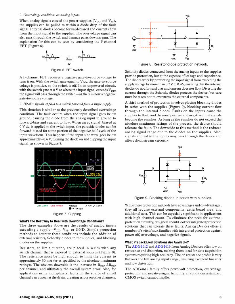
Analog Dialogue 45-05, May (2011) 3
2. Overvoltage conditions on analog inputs.
When analog signals exceed the power supplies (VDD and VSS), the supplies can be pulled to within a diode drop of the fault signal. Internal diodes become forward-biased and currents flow from the input signal to the supplies. The overvoltage signal can also pass through the switch and damage parts downstream. The explanation for this can be seen by considering the P-channel FET (Figure 6).
0V
0V 0V
Figure 6. FET switch.
A P-channel FET requires a negative gate-to-source voltage to turn it on. With the switch gate equal to VDD, the gate-to-source voltage is positive, so the switch is off. In an unpowered circuit, with the switch gate at 0 V or where the input signal exceeds VDD, the signal will pass through the switch—as there is now a negative gate-to-source voltage.
3. Bipolar signals applied to a switch powered from a single supply.
This situation is similar to the previously described overvoltage condition. The fault occurs when the input signal goes below ground, causing the diode from the analog input to ground to forward-bias and current to flow. When an ac signal, biased at 0 V dc, is applied to the switch input, the parasitic diodes can be forward-biased for some portion of the negative half-cycle of the input waveform. This happens if the input sine wave goes below approximately –0.6 V, turning the diode on and clipping the input signal, as shown in Figure 7.
CH1 2.00V CH2 100mV M200𝛍𝛍s A CH1 3.00V
1
T –36.0𝛍𝛍s
T
CLIPPINGSWITCHSIGNALRANGE
SOURCE INPUT:∙5V SINE WAVE
VDD = 0V
GND = 0V
DRAIN OUTPUT:CLIPPED SIGNAL
∙5V INPUT
Figure 7. Clipping.
What’s the Best Way to Deal with Overvoltage Conditions?The three examples above are the results of analog inputs exceeding a supply—VDD, VSS, or GND. Simple protection methods to counter these conditions include the addition of external resistors, Schottky diodes to the supplies, and blocking diodes on the supplies.
Resistors, to limit current, are placed in series with any switch channel that is exposed to external sources (Figure 8). The resistance must be high enough to limit the current to approximately 30 mA (or as specified by the absolute maximum ratings). The obvious downside is the increase in RON, ∆RON, per channel, and ultimately the overall system error. Also, for applications using multiplexers, faults on the source of an off channel can appear at the drain, creating errors on other channels.
VSS
RL
VDD
GND
GND
DS
Figure 8. Resistor-diode protection network.
Schottky diodes connected from the analog inputs to the supplies provide protection, but at the expense of leakage and capacitance. The diodes work by preventing the input signal from exceeding the supply voltage by more than 0.3 V to 0.4 V, ensuring that the internal diodes do not forward bias and current does not flow. Diverting the current through the Schottky diodes protects the device, but care must be taken not to overstress the external components.
A third method of protection involves placing blocking diodes in series with the supplies (Figure 9), blocking current flow through the internal diodes. Faults on the inputs cause the supplies to float, and the most positive and negative input signals become the supplies. As long as the supplies do not exceed the absolute maximum ratings of the process, the device should tolerate the fault. The downside to this method is the reduced analog signal range due to the diodes on the supplies. Also, signals applied to the inputs may pass through the device and affect downstream circuitry.
VSS
VSRL
VDD
GND
DS
Figure 9. Blocking diodes in series with supplies.
While these protection methods have advantages and disadvantages, they all require external components, extra board area, and additional cost. This can be especially significant in applications with high channel count. To eliminate the need for external protection circuitry, designers should look for integrated protection solutions that can tolerate these faults. Analog Devices offers a number of switch/mux families with integrated protection against power off, overvoltage, and negative signals.
What Prepackaged Solutions Are Available?The ADG4612 and ADG4613 from Analog Devices offer low on resistance and distortion, making them ideal for data acquisition systems requiring high accuracy. The on resistance profile is very flat over the full analog input range, ensuring excellent linearity and low distortion.
The ADG4612 family offers power-off protection, overvoltage protection, and negative-signal handling, all conditions a standard CMOS switch cannot handle.

4 Analog Dialogue 45-05, May (2011)
When no power supplies are present, the switch remains in the off condition. The switch inputs present a high impedance, limiting current flow that could damage the switch or downstream circuitry. This is very useful in applications where analog signals may be present at the switch inputs before the power is turned on, or where the user has no control over the power supply sequence. In the off condition, signal levels up to 16 V are blocked. Also, the switch turns off if the analog input signal level exceeds VDD by VT.
SX
SX DX INX VDD
DX
OVMONITOR
DIGITALINPUT
PSMONITOR
Figure 10. ADG4612/ADG4613 switch architecture.
Figure 10 shows a block diagram of the family’s power-off protection architecture. Switch source- and drain inputs are constantly monitored and compared to the supply voltages, VDD and VSS. In normal operation the switch behaves as a standard CMOS switch with full rail-to-rail operation. However, during a fault condition where the source or drain input exceeds a supply by a threshold voltage, internal fault circuitry senses the overvoltage condition and puts the switch in isolation mode.
Analog Devices also offers multiplexers and channel protectors that can tolerate overvoltage conditions of +40 V/–25 V beyond the supplies with power (±15 V) applied to the device, and +55 V/–40 V unpowered. These devices are specifically designed to handle faults caused by power-off conditions.
VSS
VSS
VDD VDD
NMOS NMOS
PMOS
PMOS
Figure 11. High-voltage fault-protected switch architecture.
These devices comprise N-channel, P-channel, and N-channel MOSFETs in series, as illustrated in Figure 11. When one of the analog inputs or outputs exceeds the power supplies, one of the MOSFETs switches off, the multiplexer input (or output) appears as an open circuit, and the output is clamped to within the supply rail, thereby preventing the overvoltage from damaging any circuitry following the multiplexer. This protects the multiplexer, the circuitry it drives, and the sensors or signal sources that drive the multiplexer. When the power supplies are lost (through, for example, battery disconnection or power failure) or momentarily disconnected (rack system, for example), all transistors are off and the current is limited to subnanoampere levels. The ADG508F, ADG509F, and ADG528F include 8:1 and dif ferential 4:1 multiplexers with such functionality.
The ADG465 single- and ADG467 octal channel protectors have the same protective architecture as these fault-protected multiplexers, without the switch function. When powered, the channel is always in the on condition, but in the event of a fault, the output is clamped to within the supply voltages.
LATCH-UP What Is a Latch-Up Condition?Latch-up may be defined as the creation of a low-impedance path between power supply rails as a result of triggering a parasitic device. Latch-up occurs in CMOS devices: intrinsic parasitic devices form a PNPN SCR structure when one of the two parasitic base-emitter junctions is momentarily forward-biased (Figure 12). The SCR turns on, causing a continuing short between the supplies. Triggering a latch-up condition is serious: in the “best” case, it leads to device malfunction, with power cycling required to restore the device to normal operation; in the worst case, the device (and possibly power supply) can be destroyed if current flow is not limited.
RS
Q2Q1
N-WELL
P– SUBSTRATE
RW
P+N+P+N+ N+P+
VSS/GNDI/O I/O I/OI/OVDD
Q1
Q2
I/O VDD
I/OVSS/GND
RW
RS
(a)
(b)
Figure 12. Parasitic SCR structure: a) device b) equivalent circuit.
The fault and overvoltage conditions described earlier are among the common causes of triggering a latch-up condition. If signals on the analog or digital inputs exceed the supplies, a parasitic transistor is turned on. The collector current of this transistor causes a voltage drop across the base emitter of a second parasitic transistor, which turns the transistor on, and results in a self-sustaining path between the supplies. Figure 12(b) clearly shows the SCR circuit structure formed between Q1 and Q2.
Events need not last long to trigger latch-up. Short-lived transients, spikes, or ESD events may be enough to cause a device to enter a latch-up state.
Latch-up can also occur when the supply voltages are stressed beyond the absolute maximum ratings of the device, causing internal junctions to break down and the SCR to trigger.
The second triggering mechanism occurs if a supply voltage is raised enough to break down an internal junction, injecting current into the SCR.
What’s the Best Way to Deal with Latch-Up Conditions?Protection methods against latch-up include the same protection methods recommended to address overvoltage conditions. Adding current-limiting resistors in the signal path, Schottky
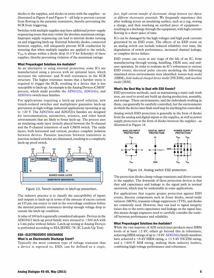
Analog Dialogue 45-05, May (2011) 5
diodes to the supplies, and diodes in series with the supplies—as illustrated in Figure 8 and Figure 9—all help to prevent current from flowing in the parasitic transistors, thereby preventing the SCR from triggering.
Switches with multiple supplies may have additional power-supply sequencing issues that may violate the absolute maximum ratings. Improper supply sequencing can lead to internal diodes turning on and triggering latch-up. External Schottky diodes, connected between supplies, will adequately prevent SCR conduction by ensuring that when multiple supplies are applied to the switch, VDD is always within a diode drop (0.3 V for Schottky) of these supplies, thereby preventing violation of the maximum ratings.
What Prepackaged Solutions Are Available?As an alternative to using external protection, some ICs are manufactured using a process with an epitaxial layer, which increases the substrate- and N-well resistances in the SCR structure. The higher resistance means that a harsher stress is required to trigger the SCR, resulting in a device that is less susceptible to latch-up. An example is the Analog Devices iCMOS® process, which made possible the ADG121x, ADG141x, and ADG161x switch/mux families.
For applications requiring a latch-up proof solution, new trench-isolated switches and multiplexers guarantee latch-up prevention in high-voltage industrial applications operating at up to ±20 V. The ADG541x and ADG521x families are designed for instrumentation, automotive, avionics, and other harsh environments that are likely to foster latch-up. The process uses an insulating oxide layer (trench) placed between the N-channel and the P-channel transistors of each CMOS switch. The oxide layers, both horizontal and vertical, produce complete isolation between devices. Parasitic junctions between transistors in junction-isolated switches are eliminated, resulting in a completely latch-up proof switch.
VG
N– P–
P-CHANNEL
BURIED OXIDE LAYER
VG
N-CHANNEL
SUBSTRATE (BACKGATE)
I/O I/O I/O I/O
P+ P+ N+ N+TRENCH
TRENCH
TRENCH
Figure 13. Trench isolation in latch-up prevention.
The industry practice is to classify the susceptibility of inputs and outputs to latch-up in terms of the amount of excess current an I/O pin can source or sink in the overvoltage condition before the internal parasitic resistances develop enough voltage drop to sustain the latch-up condition.
A value of 100 mA is generally considered adequate. Devices in the ADG5412 latch-up proof family were stressed to ±500 mA with a 1-ms pulse without failure. Latch-up testing at Analog Devices is performed according to EIA/JEDEC-78 (IC Latch-Up Test).
ESD—ELECTROSTATIC DISCHARGE What Is an Electrostatic Discharge Event?Typically the most common type of voltage transient that a device is exposed to, ESD, can be def ined as a single,
fast, high-current transfer of electrostatic charge between two objects at different electrostatic potentials. We frequently experience this after walking across an insulating surface, such as a rug, storing a charge, and then touching an earthed piece of equipment—resulting in a discharge through the equipment, with high currents flowing in a short space of time.
ICs can be damaged by the high voltages and high peak currents generated by an ESD event. The effects of an ESD event on an analog switch can include reduced reliability over time, the degradation of switch performance, increased channel leakage, or complete device failure.
ESD events can occur at any stage of the life of an IC, from manufacturing through testing, handling, OEM user, and end-user operation. In order to evaluate an IC’s robustness to various ESD events, electrical pulse circuits modeling the following simulated stress environments were identified: human body model (HBM), field-induced charged device model (FICDM), and machine model (MM).
What’s the Best Way to Deal with ESD Events?ESD prevention methods, such as maintaining a static-safe work area, are used to avoid any build up during production, assembly, and storage. These environments, and the individuals working in them, can generally be carefully controlled, but the environments in which the device later finds itself may be anything but controlled.
Analog switch ESD protection is generally in the form of diodes from the analog and digital inputs to the supplies, as well as power supply protection in the form of diodes between the supplies—as illustrated in Figure 14.
S D IN GND
ANALOG INPUTPROTECTION
DIGITAL INPUTPROTECTION
POWER SUPPLYPROTECTION
GND
VLVDD VDD VDD
VSS VSS VSS
Figure 14. Analog switch ESD protection.
The protection diodes clamp voltage transients and divert current to the supplies. The downside of these protection devices is that they add capacitance and leakage to the signal path in normal operation, which may be undesirable in some applications.
For applications that require greater protection against ESD events, discrete components such as Zener diodes, metal-oxide varistors (MOVs), transient voltage suppressors (TVS), and diodes are commonly used. However, they can lead to signal integrity issues due to the extra capacitance and leakage on the signal line; this means design engineers need to carefully consider the trade-off between performance and reliability.
What Prepackaged Solutions Are Available?While the vast majority of ADI switch/mux products meet HBM levels of at least ±2 kV, others go beyond this in robustness, achieving HBM ratings of up to ±8 kV. ADG541x family members have achieved a ±8-kV HBM rating, a ±1.5-kV FICDM rating, and a ±400-V MM rating, making them industry leaders, combining high-voltage performance and robustness.

6 Analog Dialogue 45-05, May (2011)
Switch/mux products, like devices mentioned here, are available with integrated protection, allowing designers to eliminate external protection circuitry, reducing the number and cost of components in board designs. Savings are even more significant in applications with high channel count.
Ultimately, using switches with fault protection, overvoltage protection, immunity to latch-up, and a high ESD rating yields a robust product that meets industry regulations and enhances customer and end-user satisfaction.
AuthorMichael Manning [[email protected]]graduated from National University of Ireland, Galway, with a BSc in appl ied physics and electronics. In 2006, he joined Analog Devices as an applications engineer in the switch/multiplexer group in Limerick, Ireland. Previously, Michael spent five years as a design and applications engineer in the automotive division at ALPS Electric in Japan and Sweden.
ConclusionWhen switch or multiplexer inputs come from remotely located sources, there is an increased likelihood that faults can occur. Overvoltage conditions may occur due to systems with poorly designed power-supply sequencing or where hot-plug insertion is a requirement. In harsh electrical environments, transient voltages due to poor connections or inductive coupling may damage components if not protected. Faults can also occur due to power-supply failures where power connections are lost while switch inputs remain exposed to analog signals. Significant damage may result from these fault conditions, possibly causing damage and requiring expensive repairs. While a number of protective design techniques are used to deal with faults, they add extra cost and board area and often require a trade-off in switch performance; and even with external protection implemented, downstream circuitry is not always protected. Since analog switches and multiplexers are often a module’s most likely electronic components to be subjected to a fault, it is important to understand how they behave when exposed to conditions that exceed the absolute maximum ratings.
APPENDIX ANALOG DEVICES SWITCH/MULTIPLEXER PROTECTION PRODUCTS:
High-Voltage Latch-Up Proof Switches
Part Number Configuration
Number of Switch Functions
RON (𝛀)
Max Analog Signal Range
Charge Injection
(pC)
On Leakage @ 85°C
(nA) Supply Voltages PackagesPrice @ 1k
($U.S.)
ADG5212 SPST/NO 4 160 VSS to VDD
0.07 0.25 Dual (±15 V), Dual (±20 V),Single (+12 V), Single (+36 V)
CSP, SOP 2.18
ADG5213 SPST/NO-NC 4 160 VSS to
VDD0.07 0.25 Dual (±15 V), Dual (±20 V),
Single (+12 V), Single (+36 V)CSP, SOP 2.18
ADG5236 SPST/NO-NC 2 160 VSS to
VDD0.6 0.4 Dual (±15 V), Dual (±20 V),
Single (+12 V), Single (+36 V)CSP, SOP 2.26
ADG5412 SPST/NO 4 9 VSS to VDD
240 2 Dual (±15 V), Dual (±20 V),Single (+12 V), Single (+36 V)
CSP, SOP 2.18
ADG5413 SPST/NO-NC 4 9 VSS to VDD
240 2 Dual (±15 V), Dual (±20 V),Single (+12 V), Single (+36 V)
CSP, SOP 2.18
ADG5433 SPST/NO-NC 3 12.5 VSS to VDD
130 4 Dual (±15 V), Dual (±20 V),Single (+12 V), Single (+36 V)
CSP, SOP 2.15
ADG5434 SPST/NO-NC 4 12.5 VSS to VDD
130 4 Dual (±15 V), Dual (±20 V),Single (+12 V), Single (+36 V)
SOP 3.04
ADG5436 SPST/NO-NC 2 9 VSS to VDD
0.6 2 Dual (±15 V), Dual (±20 V),Single (+12 V), Single (+36 V)
CSP, SOP 2.26
High-Voltage Latch-Up Proof Multiplexers
Part Number Configuration
RON (𝛀)
Max Analog Signal Range
Charge Injection
(pC)
On Capacitance
(pF)
On Leakage @ 85°C
(nA) Supply Voltages Packages
Price @ 1000 to
4999 ($U.S.)
ADG5204 (4:1) × 2 160 VSS to VDD
0.6 30 0.5 Dual (±15 V), Dual (±20 V),Single (+12 V), Single (+36 V)
CSP, SOP 2.26
ADG5408 (8:1) × 1 14.5 VSS to VDD
115 133 4 Dual (±15 V), Dual (±20 V),Single (+12 V), Single (+36 V)
CSP, SOP 2.41
ADG5409 (4:1) × 2 12.5 VSS to VDD
115 81 4 Dual (±15 V), Dual (±20 V),Single (+12 V), Single (+36 V)
CSP, SOP 2.41
ADG5404 (4:1) × 1 9 VSS to VDD
220 132 2 Dual (±15 V), Dual (±20 V),Single (+12 V), Single (+36 V)
CSP, SOP 2.26

Analog Dialogue 45-05, May (2011) 7
Low-Voltage Fault-Protected Multiplexers
Part Number Configuration
Number of Switch Functions
Max Analog Signal Range
Fault Response Time (ns)
Fault Recovery Time (𝛍s)
–3 dB Bandwidth
(MHz) PackagesPrice @ 1k
($U.S.)
ADG4612 SPST/NO 4 –5.5 V to VDD
295 1.2 293 SOP 1.84
ADG4613 SPT/NO-NC 4 –5.5 V to VDD
295 1.2 294 CSP, SOP 1.84
High-Voltage Fault-Protected Multiplexers
Part Number
Switch/Mux
Function x #
RON (𝛀)
Max Analog Signal Range
tTRANSITION(ns)
Supply Voltages (V) Power Dissipation (mW) Packages
Price @ 1000 to
4999 ($U.S.)
ADG438F (8:1) × 1 400 VSS + 1.2 V to VDD – 0.8 V 170 Dual (±15 V) 2.6 DIP, SOIC 3.68
ADG439F (4:1) × 2 400 VSS + 1.2 V to VDD – 0.8 V 170 Dual (±15 V) 2.6 DIP, SOIC 3.68
ADG508F (8:1) × 1 300 VSS + 3 V to VDD – 1.5 V 200 Dual (±12 V),
Dual (±15 V)3 DIP, SOIC 3.31
ADG509F (4:1) × 2 300 VSS + 3 V to VDD – 1.5 V 200 Dual (±12 V),
Dual (±15 V)3 DIP, SOIC 3.31
ADG528F (8:1) × 1 300 VSS + 3 V to VDD – 1.5 V 200 Dual (±12 V),
Dual (±15 V)3 DIP, LCC 3.91
High-Voltage Channel Protectors
Part Number Configuration
Number of Switch Functions
RON(𝛀)
Max Positive Supply (V)
Max Negative Supply (V) Packages
Price @ 1k ($U.S.)
ADG465 Channel Protector 1 80 20 20 SOIC, SOT 0.84ADG467 Channel Protector 8 62 20 20 SOIC, SOP 2.40