real-world applications of analog and digital evolvable
TRANSCRIPT
220 IEEE TRANSACTIONS ON EVOLUTIONARY COMPUTATION, VOL. 3, NO. 3, SEPTEMBER 1999
Real-World Applications of Analogand Digital Evolvable Hardware
Tetsuya Higuchi, Masaya Iwata, Didier Keymeulen, Hidenori Sakanashi, Masahiro Murakawa, Isamu Kajitani,Eiichi Takahashi,Member, IEEE,Kenji Toda, Mehrad Salami, Nobuki Kajihara, and Nobuyuki Otsu
Abstract—In contrast to conventional hardware where thestructure is irreversibly fixed in the design process, evolvablehardware (EHW) is designed to adapt to changes in task re-quirements or changes in the environment, through its abilityto reconfigure its own hardware structure dynamically and au-tonomously. This capacity for adaptation, achieved by employingefficient search algorithms based on the metaphor of evolution,has great potential for the development of innovative industrialapplications. This paper introduces EHW chips and six applica-tions currently being developed as part of MITI’s Real-WorldComputing Project; an analog EHW chip for cellular phones,a clock-timing architecture for Giga hertz systems, a neuralnetwork EHW chip capable of autonomous reconfiguration, adata compression EHW chip for electrophotographic printers,and a gate-level EHW chip for use in prosthetic hands and robotnavigation.
Index Terms—Evolutionary computation, evolvable hardware,prosthetics, robot navigation.
I. INTRODUCTION
ONE OF the most remarkable features of the human brainis its plasticity. It is the plasticity of this natural neural
network that makes it capable of flexible and robust infor-mation processing. This is in sharp contrast to conventionalcomputer hardware where all the circuits and interconnec-tions are fixed, making adaptive change impossible. Researchinto the development of adaptive machines is essentiallyseeking to reduce this contrast by incorporating plasticitywithin machines. The motivation behind this approach isto develop machines that can change their own hardwarestructure to adapt to new environments, and thus provide betterperformance.
There has been significant research progress in hardware-based adaptive machines, such as perceptrons, WISARD [11],and ALN (adaptive logic network) [14]. Hardware adaptation,however, has been limited in the sense that adaptation isoffline. This means that, in practice, such systems are only usedafter the adaptation or the learning phase is complete. Ideally,however, adaptive machines should be capable of changing
Manuscript received January 22, 1999; revised May 28, 1999. This workwas supported by the MITI Real World Computing Project (RWCP).
T. Higuchi, M. Iwata, D. Keymeulen, H. Sakanashi, M. Murakawa, I.Kajitani, E. Takahashi, K. Toda, and N. Otsu are with the ElectrotechnicalLaboratory, Ibaraki, 305-8568 Japan.
N. Kajihara is with NEC Laboratory, Kawasaki, 216-0033 Japan.M. Salami is with Swinburne University of Technology, Hawthorn 3122,
Australia.Publisher Item Identifier S 1089-778X(99)07198-2.
the structure of their hardware while they are operating inreal-time (i.e., online adaptation).
Evolvable hardware (EHW) is a new concept in the develop-ment of online adaptive machines. In contrast to conventionalhardware where the structure is irreversibly fixed in thedesign process, EHW is designed to adapt to changes in taskrequirements or changes in the environment through its abilityto reconfigure its own hardware structure online (dynamically)and autonomously. This capacity for adaptation, achieved byevolutionary algorithms (such as genetic algorithms (GA’s)[2], [16]), has great potential for the development of innovativeindustrial applications.
Although the concept of EHW is relatively new, some EHWapplications are already being evaluated for their commercialvalue. In this paper, we introduce five EHW chips and theirpractical applications. These are currently being developed aspart of Ministry of International Trade and Industry’s (MITI’s)Real-World Computing Project: a general-purpose EHW chip(to be used in prosthetic hands and robot navigation), a datacompression EHW chip for electrophotographic printers, aneural network EHW chip capable of autonomous reconfig-uration, an analog EHW chip for cellular phones, and anEHW-based clock-timing architecture.
Although important classifications of evolvable hardwareand bio-inspired machines have already been proposed [4],[10], in this paper a basic distinction is made between digital-hardware evolution and analog-hardware evolution. Digitalhardware evolutions may be further classified into gate-levelevolution and function-level evolution.
Much of the research on EHW has focused on gate-levelevolution: the evolution of digital-hardware involving primi-tive hardware gates, such asAND-gates andOR-gates. As twoexamples of what is possible with gate-level digital hardwareevolution, we shall introduce 1) a logic circuit that canadaptively synthesize for noise-insensitive pattern recognition,such as in a neural network and 2) a fault-tolerant controlcircuit capable of adapting to environmental changes.
These are demonstrated in the following applications. Ina prosthetic hand control application, evolvable hardware isused to implement a pattern recognition circuit tailored to theindividual user. The hand is operated using electromyograph(EMG) signals from the skin surface. The mapping of EMGpatterns to desired hand actions is done with the EHW-based pattern recognition circuit, which is capable of noise-insensitive recognition. Because EMG patterns have strongindividual differences and may change due to physical body
1089–778X/99$10.00 1999 IEEE

HIGUCHI et al.: ANALOG AND DIGITAL EVOLVABLE HARDWARE 221
conditions, hardware designers cannot design such circuitsin advance using the conventional approach to hardwaredesign, where design specifications must be identified earlyin the design process. This is a typical example of where thehardware is required to be adaptive.
As a second application of gate-level evolution, mobilerobot navigation is described. In the robot, the EHW worksas a Boolean controller that accepts sensory inputs and gen-erates wheel motor commands. The task is to track a movingtarget represented by a colored ball, while avoiding obstaclesduring its motion in a nondeterministic and nonstationaryenvironment. For example, even if some of the sensors of therobot are intentionally broken, the controller on the EHW isreconfigured to continue tracking the ball with the remainingfunctional sensors. This demonstrates how EHW can adapt toenvironmental changes effectively. After discussing these twoapplications, we shall describe the digital EHW chip, whichincludes GA hardware, reconfigurable logic gates, and a CPUcore.
A data compression chip for electrophotographic printers isalso described as a further example of more dedicated gate-level EHW chips. The data compression algorithm used in thischip is based on predictions made for image data to be sent tothe printer. The accuracy of the predictions is a major factor indetermining data compression ratios, since higher ratios can beobtained when the prediction is more precise. Prediction accu-racy varies according to the data content, however, and thusthis needs to be tailored to the specific data to be compressed.In this application, EHW is used as adaptive prediction hard-ware for efficient data compression, making it possible to attaincompression ratios that are double those obtainable with theexisting international standards in lossless data compression.Furthermore, because decompression is also performed quicklywith the EHW, it is possible to satisfy the fast-printing-speedrequirements of electrophotopgraphic printers.
In function-level evolution, hardware synthesis involveshigher-level hardware functions than the primitive gates (e.g.,AND-gates) of gate-level evolution. With function-level evo-lution, it is possible 1) to synthesize more useful hardwarefunctions and 2) to design larger hardware circuits than ispossible with gate-level evolution.
An autonomously reconfigurable neural network chip isdescribed as an example of function-level EHW. In neuralnetwork processing, the tasks of determining the topology ofthe network and assigning appropriate functions to the nodesheavily influence learning times and learning performance. Asyet, however, there is no solid theoretical basis for determiningboth topology and node functions. The GA in the chip candetermine both of the topology and node functions that aremost suitable to a given problem.
In contrast to digital-hardware evolution, analog-hardwareevolution is a relatively new concept. This new paradigmwithin EHW is growing rapidly and is very close to indus-trialization. As an example of this, an analog EHW chip forcellular phones is described. Although the chip works in offlineevolution mode, this approach has two advantages: 1) highyield rates and 2) smaller circuit size, leading to lower powerconsumption and lower manufacturing costs.
A second example of analog hardware evolution is a clock-timing architecture for very high-speed digital systems, whichare close to gigahertz speeds. In such high-speed large scale in-tegrations (LSI’s), precision in clock distribution is extremelydifficult to maintain, leading to poor yield rates. The EHW-based clock architecture, which has been implemented in atest chip, enables genetic adjustments in timing to be madethroughout the chip.
This paper is organized as follows. Section II describes thebasic concepts of EHW. Section III details two applicationsof gate-level evolution and a general-purpose digital EHWchip. In Section IV, a special-purpose EHW chip for datacompression is discussed as an example of the industrial use ofEHW. As an example of function-level evolution, Section Vdescribes an EHW-based neural network chip. Section VIprovides details of the analog EHW chip for cellular phones.Section VII describes the EHW-based clock timing architec-ture, followed by the conclusion.
II. EVOLVABLE HARDWARE: BASIC CONCEPTS
Evolvable hardware is based on the idea of combiningreconfigurable hardware devices with evolutionary algorithms,such as GA’s [4], [6]. There are a variety of ways in whichreconfigurable hardware and evolutionary algorithms can becombined, depending on the purposes of the evolved hardware.
When innovative solutions to difficult hardware designproblems are required [26], genetic programming may be usedto create hardware design in terms of hardware descriptionlanguages (HDL’s) [25], [30]. As this kind of genetic pro-gramming requires a great deal of time, however, it is bestsuited to offline evolution.
On the other hand, when online evolution is required,then evolution speed becomes a critical factor. In such cases,direct manipulation of the hardwire structure by GA’s is moresuitable. In line with our emphasis on online evolution, thiswill be the focus of our discussions below.
The structure of a reconfigurable hardware device canbe changed any number of times by downloading into thedevice a software bit string called configuration bits. (fFieldprogrammable gate arrays (FPGA’s) and programmable logicdevices (PLD’s) are typical examples of reconfigurable hard-ware devices.
Fig. 1 shows the simplified structure of a commercial PLDcalled GAL [5]. GAL consists of a fuse array and a logic cell.GAL also has a configuration bit register that determines thelink settings to implement a particular hardware structure in theGAL. The fuse array is used to determine the interconnectionsbetween the device inputs (e.g., P2 in Fig. 1) and a logic cell,as well as to specify theAND-term inputs to the logic cell.If a link on a particular row of a fuse array is connected(shown as a dot in Fig. 1), then the corresponding inputsignal is connected to the row. When a link is connected, thecorresponding bit in the configuration bit register is set to one.The input signal then becomes one of theAND-term members.For example, the input signals P3 and P5 are connected to thefirst row, because the corresponding fuse links are connected.These inputs generate theAND-term, P3 P5. The logic cellcan select a predetermined function, such as anAND gate,

222 IEEE TRANSACTIONS ON EVOLUTIONARY COMPUTATION, VOL. 3, NO. 3, SEPTEMBER 1999
Fig. 1. The structure of PLD.
an OR gate, or a flip-flop, by specifying some bits in theconfiguration bit register. Thus, according to the content ofthe configuration bit register, arbitrary hardware functions canbe implemented in the GAL.
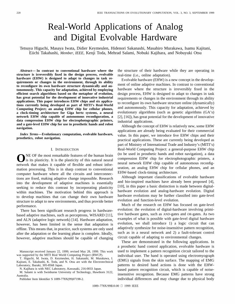
A GA is a robust search algorithm loosely based on popula-tion genetics. It effectively seeks solutions from a vast searchspace at reasonable computation costs. The basic conceptbehind the combination of these two elements in EHW isto regard the configuration bits for reconfigurable hardwaredevices as chromosomes for GA’s (see Fig. 2). If a fitnessfunction is properly designed for a task, then the GA’s canautonomously find the best hardware configuration in terms ofthe chromosomes (i.e., configuration bits).
To give a basic idea of how the hardware evolution pro-ceeds, let us take the example of image data compression.For image data compression using EHW, we use a predictionfunction. Optimal prediction functions vary greatly accordingto the characteristics of data to be compressed. Some data mayinclude many different shapes and colors, but some may bemore plain. It is, therefore, not possible to design in advance aprediction hardware function. Instead of specifying a detailedhardware design, we define a fitness function to allow theEHW to autonomously and adaptively reconfigure itself for themost suitable prediction hardware. For this purpose, the datacompression ratio is used as a fitness function. Accordingly,a prediction function circuit with a higher data compressionratio is likely to remain in a population. When a goodchromosome is obtained, it is immediately downloaded intothe reconfigurable device.
If the prediction performance of a given EHW is reduceddue to changes in the nature of the data to be compressed, thenthe GA process is invoked and the search for a better hardwarestructure of prediction is initiated. In this way, EHW is capableof both autonomous and dynamic hardware reconfigurations.Below we show how this characteristic of EHW is utilized infive EHW chips and their applications.
III. GATE-LEVEL EHW APPLICATIONS
AND CHIP ARCHITECTURE
This section describes two applications using gate-levelevolution and the architecture of a general purpose EHW chipbased on gate-level evolution.
A. Myoelectric Prosthetic Hand Controller with EHW
1) Background: Although limited to a simple recognitiontask, Iwata’s work in character recognition has demonstratedthat EHW is capable of performing the noise-insensitivepattern recognition task as well as in neural networks [9].This work was inspired by Armstrong’s ALN which demon-strated that Boolean logic can be employed to deal withnoise-insensitive pattern recognition [14]. Using EHW, morecompact implementations and faster processing speeds arepossible than with neural networks.
The myoelectric prosthetic hand control is our secondapplication in this direction (our first being the characterrecognition). The myoelectric hand is operated by the sig-nals generated with muscular movements (electromyography,EMG) [20]. It takes a long time, however, usually almostone month, before a disabled person is able to control amultifunction prosthetic hand freely. During this period, thedisabled person has to undertake training to adapt to themyoelectric hand. We have reversed this situation by havingthe myoelectric hand adapt itself to the disabled person andthus drastically reduce this training period.
Although work is being carried out on applying neural net-works for adaptable prosthetic hand controllers, this approachis not very promising due to implementation problems becausesystems using neural networks are large and thus difficult toimplement within a prosthetic hand.
In contrast, the system using the EHW is suitable for thisapplication, because of its compactness and high-speed adapt-ability. The adaptation speed with EHW is usually less than10 min, which is a significant improvement as compared withother systems (e.g., one month). It has, therefore, been decidedthat the EHW-based prosthetic hand will be commercialized.
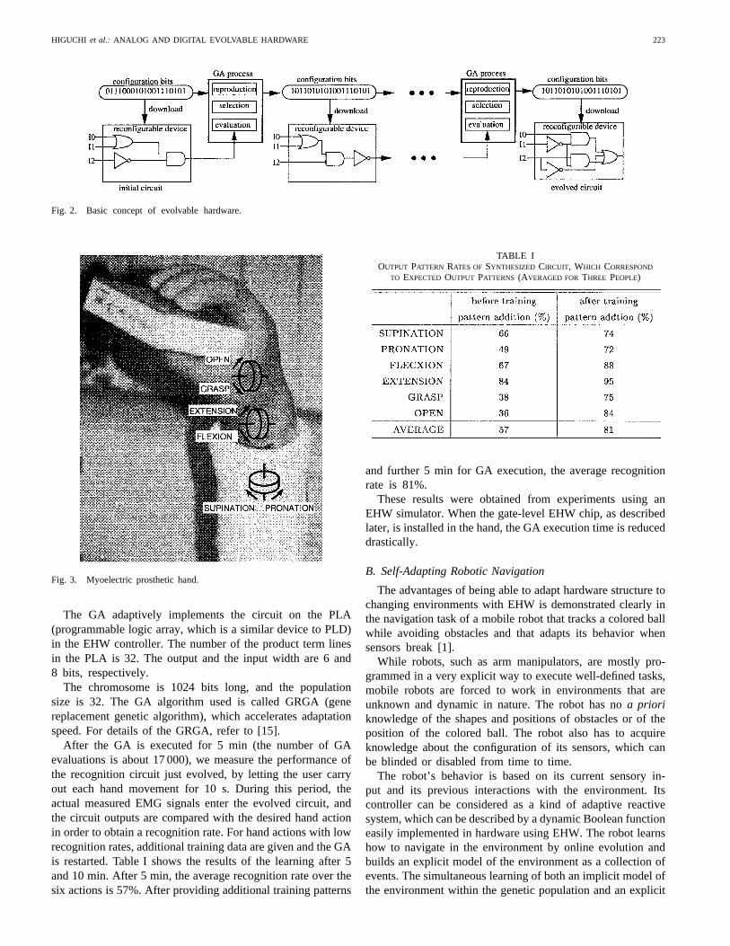
2) The EHW Learning Method and Its Performance:Themyoelectric hand used in this work is able to perform thesix actions (Fig. 3), which are paired (open-grasp, supination-pronation, and flexion-extension), with a separate motor con-trol for each pair. The task for the EHW controller is tosynthesize pattern recognition hardware to map input patterns(i.e., feature vectors for two-channel EMG signals), to thedesired actions of the hand (i.e., one of the six actions).
Because EMG signals vary greatly between individuals,however, it is impossible to design such a recognition circuit inadvance. Furthermore, even for a particular person, the featurevectors of the EMG signals sometimes may change even overshort periods. Therefore, the control hardware circuit must besynthesized adaptively.
Circuit synthesis is carried out as follows. First, trainingpattern data is obtained in an online fashion, where the handuser makes one of the six actions from which we measure tenEMG signal patterns. For all six actions, therefore, we obtain aset of 60 signals as training data. Then, based on this obtainedtraining data, circuit synthesis is started using a GA.
HIGUCHI et al.: ANALOG AND DIGITAL EVOLVABLE HARDWARE 223
Fig. 2. Basic concept of evolvable hardware.
Fig. 3. Myoelectric prosthetic hand.
The GA adaptively implements the circuit on the PLA(programmable logic array, which is a similar device to PLD)in the EHW controller. The number of the product term linesin the PLA is 32. The output and the input width are 6 and8 bits, respectively.
The chromosome is 1024 bits long, and the populationsize is 32. The GA algorithm used is called GRGA (genereplacement genetic algorithm), which accelerates adaptationspeed. For details of the GRGA, refer to [15].
After the GA is executed for 5 min (the number of GAevaluations is about 17 000), we measure the performance ofthe recognition circuit just evolved, by letting the user carryout each hand movement for 10 s. During this period, theactual measured EMG signals enter the evolved circuit, andthe circuit outputs are compared with the desired hand actionin order to obtain a recognition rate. For hand actions with lowrecognition rates, additional training data are given and the GAis restarted. Table I shows the results of the learning after 5and 10 min. After 5 min, the average recognition rate over thesix actions is 57%. After providing additional training patterns
TABLE IOUTPUT PATTERN RATES OF SYNTHESIZED CIRCUIT, WHICH CORRESPOND
TO EXPECTED OUTPUT PATTERNS (AVERAGED FOR THREE PEOPLE)
and further 5 min for GA execution, the average recognitionrate is 81%.
These results were obtained from experiments using anEHW simulator. When the gate-level EHW chip, as describedlater, is installed in the hand, the GA execution time is reduceddrastically.
B. Self-Adapting Robotic Navigation
The advantages of being able to adapt hardware structure tochanging environments with EHW is demonstrated clearly inthe navigation task of a mobile robot that tracks a colored ballwhile avoiding obstacles and that adapts its behavior whensensors break [1].
While robots, such as arm manipulators, are mostly pro-grammed in a very explicit way to execute well-defined tasks,mobile robots are forced to work in environments that areunknown and dynamic in nature. The robot has noa prioriknowledge of the shapes and positions of obstacles or of theposition of the colored ball. The robot also has to acquireknowledge about the configuration of its sensors, which canbe blinded or disabled from time to time.
The robot’s behavior is based on its current sensory in-put and its previous interactions with the environment. Itscontroller can be considered as a kind of adaptive reactivesystem, which can be described by a dynamic Boolean functioneasily implemented in hardware using EHW. The robot learnshow to navigate in the environment by online evolution andbuilds an explicit model of the environment as a collection ofevents. The simultaneous learning of both an implicit model ofthe environment within the genetic population and an explicit

224 IEEE TRANSACTIONS ON EVOLUTIONARY COMPUTATION, VOL. 3, NO. 3, SEPTEMBER 1999
Fig. 4. Autonomous mobile robot.
model can reduce the number of fitness evaluations required inthe real physical environment because the fitness evaluationscan be carried out using the explicit model. The reduction inthe number of required interactions together with the fact thatthe fitness evaluations are executed using evolvable hardwarehas the advantage of speeding up the adaptive process.
1) The Robot and Its Environment:The robot shape is cir-cular with a diameter of 25 cm (Fig. 4). It has ten proximityinfrared sensors of 1-bit resolution equally distributed aroundits periphery (Fig. 5). These sensors indicate the presence ofobjects at distances of less than 30 cm, yielding 10 bits ofsensory input to the reactive robot controller. Two camerasare mounted on the top of the robot in order to locate thetarget within the four 90 sectors around the robot. The sectornumber locating the target is represented with 2 bits of sensoryinput. Thus, 12 bits of sensory input (proximity: 10 bits, targetdirection: 2 bits) are provided to the reactive robot controllerwhich is implemented by one EHW circuit.
The output of the reactive controller is a 3-bit motor com-mand to determine the motion of the robot. The robot movesusing two independent motor wheels, which are controlledin terms of speed. This allows the robot to perform eightpreprogrammed motions: two translations, two rotations, andfour combinations of rotation and translation.
The robot is controlled by a TMS 320 C44 board connectedto one transputer for the infrared sensors, the vision sensor,and the motor wheels, and two evolvable-hardware circuitsthat execute the robot controller and simulate the evolutionaryprocess, respectively.
The robot also has four bumping sensors to detect when ithits an obstacle at either the front or the back. The numberof bumps during a navigation run is counted and used inthe fitness calculation to evolve the reactive robot controller,where a good navigation controller is one that yields fewerbumps.
2) EHW and Its Performance:The EHW circuit on boardthe robot implements a dynamic reactive robot controllerthat accepts 12 bits of sensory inputs and yields 3-bit wheel
motor commands. When the robot does not detect obstaclesin its neighborhood (its ten proximity sensors are allOFF), itsbehavior is preprogrammed on the EHW to go toward the ball.When the robot detects obstacles (at least one of the proximitysensors isON), the EHW implements a dynamic Booleanfunction with three FPGA Altera Flex 8000’s. The Booleanfunction is implemented in terms of a 50-term disjunctivenormal form (DNF) with an AND-array and anOR-array(Fig. 5). In our experimental setup with 12 Boolean inputsensors and three Boolean outputs, theAND–OR array has27 columns and needs a maximum number of 4096 rowsto represent any three-output Boolean function of the 12Boolean variables. To force the Boolean function to generalize,however, the number of rows can be reduced by merging rowswith the same output. Our experiments were able to reduce thenumber of rows and thus the number of terms of the DNF to50.
The configuration bit string of the 50-term DNF is 1350 bitslong while 12 144 bits are needed to represent any functionwith 12 Boolean inputs and three outputs. The 1350 bits ofthe EHW are regarded as a chromosome for the GA.
To learn with fewer interactions with the physical environ-ment and still maintain good online performance, the robot hasto do some experimentation in an approximate explicit worldmodel of the environment. Our approach consists of having therobot learn a model continually throughout its lifetime and, ateach motion, the current model is used to compute an optimalcontroller that controls the robot until it hits an obstacle orbecomes stuck. This method, first, avoids an arbitrary divisionbetween the learning phase and motion phase. Second, withthis approach the robot is able to gather data about theenvironment progressively depending on the efficiency of thecontroller. Third, the robot is able to deal with changes inthe environment or in its structure. Because this approachis extremely demanding computationally and to acceleratethe entire evolutionary process, the evolutionary process wasimplemented with evolvable hardware situated next to theevolvable hardware controlling the robot. The evolvable hard-ware evaluated a population of controllers by computingtheir Boolean functions. Each controller was evaluated in theexplicit world model using an experience replay strategy [13].The fitness function is a combination of three factors: 1) thenumber of times the robot hits an obstacle, 2) the numberof times the robot became stuck near an obstacle, and 3) thedistance covered by the robot in a fixed period of time. In ourapproach, evolution is used as an adaptive strategy searchingcontinuously for controllers to avoid bumping into the obsta-cles and becoming stuck near an obstacle, and to cover thegreatest distance in an explicit world model that is graduallychanging. The population size of the GA was 500 individuals.For the selection algorithm, we used tournament selection withtournament size 20 and an elitist algorithm. Using these threefactors and the preprogrammed behavior, the real robot wasable to reach the target by searching and switching controllersin the population every time the world model changed.
The performance of this robot navigation system is remark-able, in comparison with other autonomous robots, both interms of its adaptation speed and the degree of self-adaptation.

HIGUCHI et al.: ANALOG AND DIGITAL EVOLVABLE HARDWARE 225
Fig. 5. Reactive navigation system.
In general, within 10 min on average, the robot is able to finda set of suitable hardware configurations for the reactive robotcontroller and is able to switch dynamically, and in real-timebetween these hardware configurations to track the ball whileavoiding obstacles. This is two orders of magnitude faster thanprevious work [12].
When some of the proximity sensors are intentionallyblinded, the robot will autonomously start to search foranother set of hardware configurations for the reactive robotcontroller and within a few minutes of navigation can succeedin finding a new set of reactive controllers that allow the robotto continue tracking the ball with the remaining functionalsensors.
The EHW implementation is almost six times faster thana digital signal processor (DSP) simulation with a TI C44processor, but the speed can be improved further by employingthe EHW chip described in the next section.
C. General-Purpose EHW Chip forGate-Level Hardware Evolution
This chip was developed in April 1998 to serve as an off-the-shelf device for gate-level hardware evolution (Fig. 6). It wasdeveloped for an autonomous mobile robot and a myoelectricartificial hand.
In most research on EHW, GA’s are executed with softwareon personal computers or workstations. This makes it difficultto use EHW in situations that need circuits to be as smalland light as possible. For example, a prosthetic hand shouldbe of the same size as a human hand and weigh less than700 grams. Similar restrictions exist for autonomous mobilerobots with EHW controllers. One answer to these problemsis to integrate both the GA hardware and the reconfigurablelogic on to a single LSI chip.
Fig. 6. Gate-level EHW chip.
This has been done with the digital EHW chip, whichconsists of three components: 1) a PLA, 2) the GA hardwarewith a 2K word chromosome memory and a 2K word trainingpattern memory, and 3) a 16-bit 33 MHz CPU core (NECV30; 8086 compatible). Arbitrary logic circuits can be recon-figured dynamically on the PLA component according to thechromosomes obtained by the GA hardware. The CPU coreinterfaces with the chip’s environment and supports fitnesscalculations when necessary. The size of the GA hardware,excluding memories, is about 16K gates. In terms of gate size,this is almost one-tenth of a 32-bit CPU core (e.g., NEC V830).However, genetic operations carried out by this chip are 62times faster than on a Sun Ultra2 (200 MHz).

226 IEEE TRANSACTIONS ON EVOLUTIONARY COMPUTATION, VOL. 3, NO. 3, SEPTEMBER 1999
Fig. 7. Template for pixel prediction.
We are currently developing the next version of this chipwith lower power consumption and a smaller chip size.
IV. DATA COMPRESSIONCHIP FOR
ELECTROPHOTOGRAPHICPRINTING
Electrophotographic (EP) printing is the latest generationtechnology in the printing and publishing industry, makingit possible to print books with high-precision photo quality.An EHW-based data compression chip has been developed,and it has outperformed current international standards oflossless data compression for bilevel image data. This chip isa gate-level digital EHW dedicated to a particular application.
A. Data Compression of Electrophotographic Images
Data compression devices are essential for the design of EPprinters, which handle large amounts of data very quickly. Forexample, one A4-size EP image of 1200 dpi requires 70 MBfor storage, and EP printers process hundreds of different pagesat a speed of 100 page/min. (Note that normal color copierscan print less than 10 pages/min.) This means that to print abook with 100 pages, 7 GB of image data must be transferredto the printer at a speed of 1800 MB/min. Unfortunately,the data transfer speed of normal hard disk drives is only300 MB/min. EP printers, therefore, have to employ datacompression techniques 1) to compress image data efficientlyand 2) to reconstruct the compressed data very quickly.Moreover, the reconstructed image must be identical to theoriginal to avoid deterioration of quality, such as blurred lettersand distortions in images (lossless compression). Traditionallossless data compression techniques, however, are insufficientboth in terms of compression ratios and decompression speeds.
The EHW data compression chip can solve these two prob-lems by a precise prediction mechanism using reconfigurablehardware [3]. Image data consists of the values for manypixels. Because the value of each pixel tends to be closelyrelated to the values for neighboring pixels, it is possible topredict the value of a given pixel based on the values for itsneighboring pixels. If the value can be predicted correctly, it isnot necessary to store it separately, which represents a savingin the size of the image data. This means that compressionratios depend greatly on the precision of the predictions. Toincrease the compression ratio, it is necessary to continuallyreselect the most suitable prediction mechanism for the varyingpatterns within an image.
TABLE IICOMPARISON OF DATA COMPRESSIONRATIO
B. Prediction of Pixel Values by EHW
GA’s within the EHW can be used to determine whichpixels to refer to at prediction. The pattern of locations forsuch reference pixels is called a “template” [23]. With theoriginal image divided into a number of subimages, GA’ssearch for a set of optimal templates for the subimages. Oncea set of optimal templates has been discovered, the hardwareprediction mechanism is reconfigured accordingly. This leadsnot only to improved compression ratios but also to higherdecompression speeds, because decompression is also carriedout by the EHW hardware.
A template consists of ten pixel locations, and each locationis selected from a 32 8 area (Fig. 7). Each location isrepresented by 8 bits ( ), with 80 bits neededto indicate all ten locations for the template. The chromosomepopulation for the GA’s represents templates that are used indata compression, where the size of data after compression isassigned back to the chromosome.
Table II shows a comparison with two major internationalstandards for data compression: Lempel–Ziv (“compress”command of UNIX) and JBIG (joint bilevel image codingexperts group) [21], [22], both available on LSI chips. TheEHW chip attained compression ratios for printer imagesalmost twice those obtained by the international standards.Arrangements have already been made for this compressionmechanism to be used in a commercial EP printer.
C. Architecture of Data Compression EHW Chip
The data compression EHW chip mainly consists of twoparts: NEC V830 RISC processor (32-bit, 100 MHz) and thedata compressor (Fig. 8). The V830 controls the proceduresin data compression, runs the GA calculations, and interfaceswith the host computer. The data compressor hardware re-ceives the optimal template identified by the GA, compressesthe input image (Fig. 9), and returns the size of compresseddata to the V830 for the GA evaluation.

HIGUCHI et al.: ANALOG AND DIGITAL EVOLVABLE HARDWARE 227
Fig. 8. The organization of the data compression EHW chip.
Fig. 9. A block diagram of the data compressor.
The data compressor hardware works at 33 MHz, so theEHW chip can compress and decompress a large EP imagewithin a few minutes. Therefore, this compression chip cansatisfy the severe requirements for processing speed of EPprinters.
V. THE GRD NEURAL NETWORK CHIP
A. Overview
The GRD (genetic reconfiguration of DSP’s) chip is afunction-level evolvable hardware device designed for neuralnetwork applications [7]. The goal of the development isto liberate neural network users from the difficult designtask of identifying an optimal neural network. Using GA’s,
both the topology and the hidden-layer node functions of aneural network mapped on the GRD chips can be dynamicallyreconfigured. This online learning capability allows neuralnetworks to adapt dynamically to changing problems.
In neural network applications, optimal performance for agiven problem is obtained by creating a neural network withthe most suitable topology and the most appropriate nodefunctions (e.g., sigmoid function or Gaussian function [19]).Furthermore, to meet the time constraints imposed by real-time applications, neural network hardware systems need to be“tailored” to an ideal network size for a problem. In general,it is very difficult to design an optimal neural network andprocess it with scalable parallel hardware [17], [18].
With the GRD chip, however, the GA program on theRISC processor can continuously reconfigure the neural net-work topology and node functions to maintain an optimalperformance.
The GRD chip consists of a 32-bit RISC processor and abinary-tree network of 15 DSP’s. Each DSP can execute onenode function. Using a binary-tree network, multiple GRDchips can be easily connected to configure scalable neuralnetwork hardware.
In addition, because the RISC processor is incorporatedwithin the GRD chip, it does not need a host machine tocontrol these tasks. This is desirable for embedded systems inpractical industrial applications, together with its fast onlinelearning capability.
Manufacture of the GRD chip began in April 1998. Theresults of a simulation with an adaptive equalizer in digitalmobile communication have shown that execution with asingle GRD chip took 2.51 s, whereas execution on a SunUltra2 200 MHz takes 36.87 s. Planned uses for the GRD chipinclude applications that vary over time and have real-timeconstraints, such as CATV modems.
B. Genetic Learning
The neural network considered here is aimed at industrialapplications that need neural networks for the approximationof nonlinear functions.
Genetic learning determines the network topology (e.g., thenumber of nodes) and the choice of node functions (e.g.,Gaussian or sigmoid function) adaptively for a given appli-cation. The initial values of the weights and the parameters ofthe node functions are also determined by the GA and thentuned by local learning with the steepest descent method.
Fig. 10 illustrates this genetic learning. A chromosome forthe GA represents one network. The network is evolved byapplying genetic operators to the chromosomes. For example,Fig. 10 shows how a network with (a) two hidden layer nodesis evolved to have (b) 15 nodes.
Here, we show how the network obtained by the GA ismapped onto the GRD chips and how they are reconfigureddynamically using the example in Fig. 10. The network struc-ture obtained by the GA is immediately mapped onto theGRD chips. For example, a neural network having a Gaussianfunction and a sigmoid function, as in Fig. 10(a), can bemapped onto the GRD chip, as in Fig. 10(c).

228 IEEE TRANSACTIONS ON EVOLUTIONARY COMPUTATION, VOL. 3, NO. 3, SEPTEMBER 1999
Fig. 10. Genetic learning with the GRD chip.
The functions and tree height in the GRD chips are dynam-ically controlled by rewriting the chromosomes on the chips.For example, in Fig. 10(c), the output of the GRD chip isconnected to the output of DSP no. 2. After evolution, inFig. 10(d), the output of the GRD chip is reconfigured to beconnected to the output of DSP no. 4. Also, in Fig. 10(c),DSP no. 5 calculates a sigmoid function. After evolution, inFig. 10(d), this DSP is reconfigured to calculate a Gaussianfunction.
Binary tree connections are very useful when a summationof node outputs is to be calculated. All the DSP’s in Fig. 10(d)are configured to conduct the summation in parallel. Forexample, DSP no. 2 calculates a Gaussian function first andthen adds the result to the output from DSP’s Nos. 1 and 5.
The above implementation is for the fastest computation.For slower applications, one GRD chip suffices to process
more than 15 nodes. A DSP in the GRD chip can process upto 84 neurons in time multiplexing.
C. The GRD Architecture and the Performance
The GRD chip consists of a 100 MHz 32-bit RISC processorand 15 DSP’s. Fig. 11 gives the overall structure of theGRD chip. The RISC processor is a NEC V830 which isdesigned for multimedia applications. The DSP, a 33 MHz16-bit fixed-point processor, is called a programmable functionunit (PFU). Fifteen PFU’s are connected in a reconfigurablenetwork with a binary tree shape. The GRD chip acceptseight 16-bit inputs and generates a 16-bit output with theMIMD parallel processing of the 15 PFU’s. The tree shapeinterconnections are powerful, especially when the summationof neuron outputs is calculated.

HIGUCHI et al.: ANALOG AND DIGITAL EVOLVABLE HARDWARE 229
Fig. 11. Overview of the GRD chip.
The GRD chip includes the V830 RISC processor to per-form the genetic reconfiguration of the PFU’s. This means thatthe GRD chip can reconfigure itself. In the PFU, a contentaddressable memory (CAM) is employed to accelerate thecomputation of nonlinear functions (e.g., sigmoid function andGaussian). Consequently the GRD chip attains a 319 MCPS(mega connection per second) performance in a multilayerperceptron (MLP).
The GRD chip can process up to 1260 neurons (84 neuronsper PFU). To configure a scalable hardware system easily,GRD chips can be connected directly to each other viaFIFO buffers inside the PFU. For example, a 19-in rackimplementation of 16 VME triple-height boards (nine GRDchips on a board) can achieve the performance of 46 GCPS(giga connection per second) in a MLP.
Simulation results of two applications (chaotic time seriesprediction and adaptive equalization in digital mobile commu-nication) show that the performance of the GRD chip is almostten times faster than a Pentium II processor of 400 MHz.
VI. A NALOG EHW CHIP FOR CELLULAR PHONE
A. Overview
Due to the remarkable advances in recent CPU’s and DSP’s,applications with analog circuits are rapidly being replacedwith digital computing. There are still many applications thatrequire high-speed analog circuits. Communication is one suchapplication.
An inherent problem in implementing analog circuits is thatthe values of the manufactured analog circuit components,such as resistors and capacitors, will often differ from theprecise design specifications. Such discrepancies cause seri-ous problems for high-end analog circuit applications. For
example, in intermediate frequency (IF) filters [24], which arewidely used in cellular phones, even a 1% discrepancy fromthe center frequency is unacceptable. It is therefore necessaryto carefully examine the analog circuit and to discard thosewhich do not meet the specifications.
The analog EHW chip for IF filters can correct thesevariations in analog-circuit values by GA’s [8]. Using this chipprovides us with two advantages. The first is an improvedyield rate. If an analog EHW chip is found not to satisfythe specifications, it can be corrected before shipping. Thisis done by executing the GA in the LSI tester at the factoryto alter the defective analog circuit components in line withthe specifications.
The second advantage is smaller circuits. One way toincrease the precision of component values in analog LSI’shas been to use large-valued analog components. This involveslarger circuits and accordingly higher manufacturing costs andgreater power consumption. With the EHW chip, however,the size of the analog circuits can be made smaller. Obvi-ously, smaller IF filters are particularly welcome in cellularphones, but similar considerations exist in a wide variety ofapplications where analog circuits are used.
B. The Chip Architecture and Yield Rate
Fig. 12 illustrates the analog EHW chip, which is an inte-grated -C IF filter. The filter chip is fabricated in a 0.8
m CMOS process. The active area of the filter is 17 mm.The specifications are shown in Fig. 14. The filter has a passbandwidth of 21.0 kHz centered at 455 kHz, and stop bandsspecified at attenuations of 48 and 65 dB. Filter gain shouldbe within the dotted lines in the figures. The3 dB pointsshould be within kHz and kHz.These specifications are very hard to satisfy, because the3

230 IEEE TRANSACTIONS ON EVOLUTIONARY COMPUTATION, VOL. 3, NO. 3, SEPTEMBER 1999
Fig. 12. Adjustment using GA’s.
Fig. 13. Schema ofGm amplifier.
(a) (b)
Fig. 14. (a) Frequency responses and (b) magnification of (a).
dB points will be outside these limits if the center frequencyis shifted even by 1%.
This IF filter has 39 parameters in total: 16 of these arerelated to the center frequency, 16 for bandwidth, and threefor filter gain. In the integrated circuit of the filter, theseparameters correspond to the transconductance of theamplifiers. The schema of a amplifier is shown in Fig. 13.
Each transconductance may differ greatly from the targetvalues, however, by up to as much as 20%.
To correct these variations, the value of the amplifiercan be set genetically. The values, which actually control thebias currents to the amplifiers, are coded as configurationbits. The GA, which is executed on an external PC, determinesthe optimal configuration bits.

HIGUCHI et al.: ANALOG AND DIGITAL EVOLVABLE HARDWARE 231
Fig. 15. EHW-based clock-timing adjusting architecture.
A chromosome for the GA consists of 39 genes thatcorrespond to the filter parameters. Each gene hasbits thatdetermine the transconductance. For example, if , thereare four transconductance values for selection by the GA’s.The genes 00, 01, 10, and 11 mean that the parameter ismultiplied by , , , and ,respectively, where is a constant value. Fitness is theweighted sum of deviations between the ideal gain and thegain obtained by the EHW chip.
In simulations, each transconductance value in the circuitwas assumed to vary from the target value by a Gaussiandistribution of %. The parameters were setto 2 and 0.025, respectively. We used a population of 50individuals, each represented by a chromosome of length 78bits. A run terminated after the fortieth generation.
Fig. 14 shows the frequency responses for the best chromo-some in a run. After iteration, the best chromosome couldsatisfy the specifications, which the initial population wasunable to meet. Out of 100 runs, 95% of the chips conformedto specifications. We have also tested 20 real chips, outof which 18 chips were successfully evolved to meet thespecifications. We are currently developing a second versionof the chip in which major circuit components are designed tobe smaller than in the present chip.
VII. A N EHW-BASED CLOCK TIMING ADJUSTING CHIP
A. Overview
The demand for high-speed LSI’s, such as Pentium III (500MHz) and DEC Alpha (600 MHz), is increasing. Unfortu-nately, the yield rates for such fast digital systems are rather
Fig. 16. Clock-timing adjuster.
poor. Typically, in the early stages of mass production, yieldrates are less than 10%. One of the reasons for the poor yieldrates is that the timing delays between digital components

232 IEEE TRANSACTIONS ON EVOLUTIONARY COMPUTATION, VOL. 3, NO. 3, SEPTEMBER 1999
Fig. 17. Evaluation function.
often do not conform to the design specifications [28]. Suchdiscrepancies arise from variations in the values of parasiticcapacitances and resistors along the data lines between digitalcomponents, which can differ significantly depending on theLSI. Variations in clock timing are referred to as “clockskew.” LSI’s that fail to satisfy design specifications becauseof clock skew are simply discarded, leading to poor yieldrates.
To solve this problem, we propose an EHW-based clock-timing adjusting architecture for high-speed digital systems[27]. Instead of simply discarding chips that do not meet thespecifications, we can genetically adjust the clock timings inthe LSI to conform to the specifications.
We have developed a LSI, which is used in the high-speedmemory tester, to show the advantages of this architecture.Simulation results show that the number of LSI’s that canoperate at 800 MHz increases from 2.9 to 51.1% after theclock-timing circuits have been evolved by the GA. This clock-timing adjusting architecture is, therefore, expected to becomea basic LSI technology for gigahertz digital systems.
B. The Chip Architecture
The proposed architecture is depicted in Fig. 15. The salientfeature of this architecture is the introduction of a delay device,to genetically adjust the clock timing, which can easily beinserted within traditional architectures.
Fig. 16 describes this clock-timing adjuster. It has quite asimple structure, consisting of a chromosome register and adelay generator. The bit-width of the chromosome registerdepends on the degree of variation in delay time.
The delay generator includes a number of smaller delaydevices, with set delays, such as one unit, two units, four units,etc., and these delay devices are connected serially. Each bitof the chromosome register corresponds to one of the smalldelay devices, and the value of the bit determines whether thedelay device is turned on or not. Taking the example depictedin Fig. 16, when the delay has a value of 10 ps, the adjusterwould generate a timing delay of 60 ps (10 ps4 + 10 ps
2) in total.
C. Genetic Learning
The traditional method for clock-timing adjustment is tocorrect clock skew. Our architecture is more precise, however,in that it seeks to correct the system to conform to thedesigner’s specifications. Adjustment proceeds as follows.
1) Load a tentative chromosome set into a chip.2) Conduct an ordinary LSI chip test and supply a se-
ries of test data with the system clock running at thespecification speed.
3) After the chip test, stop the system clock and extract allFF values.
4) Compare extracted FF values with expected values gen-erated by logical simulation.
5) Calculate the evaluation function from the comparison.6) Generate a new generation of chromosomes according
to the evaluation function.
Note here that the clock timing is not measured directly atall. This is a major advantage because the timing measurementis very costly.

HIGUCHI et al.: ANALOG AND DIGITAL EVOLVABLE HARDWARE 233
Fig. 18. Evolvable memory test pattern generator.
Fig. 19. Simulation result (distribution function).
Fig. 17 shows how to evaluate the fitness. In the figure, twoFF’s out of eight have failed to work, and the evaluation valueis 80%. Chips that do not have a fitness value of 100% areregarded as defective.
D. Simulation Study
The simulation experiments conducted to adjust clock-timing for a circuit are described next.
For the evaluation, a memory test pattern generator, shownin Fig. 18, was selected and converted to a simulation modelfor evaluation. This is a simple, but quite important, logicblock for memory testing devices. It is used to generate accesspatterns to test memory at speeds used when accessing realmemory chips. For example, in testing memory modules forthe direct rambus systems, the testing hardware should supplyrather long test patterns at a speed of 800 MHz [29].
In the simulation, the number of sample chips was 1000, thepopulation size was 50, and the number of generations was 20.Device parameters were assumed to vary according to a normaldistribution. The results are depicted in Fig. 19. The-axisrepresents clock speed, with the percentage of chips that could
operate at a given speed, being plotted along the-axis. Themost significant result from these simulations was the findingthat 50% of the chips designed with 500 MHz clocks could beadjusted to operate at improved speeds of 800 MHz, whereasonly 2.9% could operate at such speeds before adjustment.
The LSI has been developed with bipolar technology, in-cluding 2000 gates. A testing environment is now beingdeveloped.
VIII. C ONCLUSION
Digital EHW is a key technology for the developmentof new applications, which previously could not be fullyrealized due to the lack of autonoumously reconfigurabledigital hardware. In general, applications that tend to be time-variant in nature and to have real-time constraints are suitablefor EHW, because EHW enables adaptation at the hardwarelevel, and fast execution, being accomplished by the hardwareitself.
Although reconfigurable hardware devices, such as FPGAand PLD, are spreading rapidly and the usefulness of re-configurable hardware is being more widely recognized, re-configuration in FPGA’s is not autonomous and requireshuman intervention. Thus, EHW indicates a new direction inreconfigurable hardware beyond FPGA’s.
After introducing the basic concepts of digital EHW, LSIarchitectures and their applications, we have described in thispaper two analog EHW chip applications.
The analog EHW chip for cellular phones has two advan-tages: high yield rate and smaller circuit size. These advantagescan be applied not only to IF filters but also to a wide varietyof analog LSI’s. Certainly, we envisage a number of analogLSI’s being redesigned according to EHW principles to satisfysevere requirements, especially in high-end analog systems,such as communications and sensoring.
The clock-timing adjusting architecture will be very im-portant for gigahertz digital systems, where although dis-crepancies from the design specifications are inevitable, theyare detrimental to performance. Rather than discarding chipsthat do not meet the specifications, minute adjustments can,however, be made with EHW architectures and evolutionarycomputation.
We have discussed the clock architecture within the domainof analog EHW. This is because even digital systems are heav-ily influenced by the behavior of analog circuits, particularlyin the high-frequency range. Without careful consideration ofthe analog aspects of digital systems, it will be impossible torealize high-end digital systems. In such systems, analog EHWcan play an extremely important role.
ACKNOWLEDGMENT
The authors would like to thank Dr. Ohmaki at Electrotech-nical Laboratory and Dr. Shimada at RWCP for their support.
REFERENCES
[1] D. Keymeulen, M. Iwata, Y. Kuniyoshi, and T. Higuchi, “Onlineevolution for a self-adapting robotics navigation system using evolvablehardware,”Artif. Life, vol. 4, pp. 359–393, 1999.

234 IEEE TRANSACTIONS ON EVOLUTIONARY COMPUTATION, VOL. 3, NO. 3, SEPTEMBER 1999
[2] D. E. Goldberg,Genetic Algorithms in Search, Optimization, and Ma-chine Learning. Reading, MA: Addison-Wesley, 1989.
[3] H. Sakanashi, M. Salami, M. Iwata, S. Nakaya, T. Yamauchi, T.Inuo, N. Kajihara, and T. Higuchi, “Evolvable hardware chip for highprecision printer image compression,” inProc. 15th Nat. Conf. ArtificialIntelligence (AAAI-98),Madison, WI, July 1998, pp. 486–491.
[4] X. Yao and T. Higuchi, “Promises and challenges of evolvable hard-ware,” IEEE Trans. Syst., Man, Cybern.t, C,vol. 29, Feb. 1999.
[5] Lattice Semiconductor Corporation,GAL Data Book, 1990.[6] T. Higuchi, M. Iwata, and W. Liu, Eds.,Proc. 1st Int. Conf. Evolvable
Systems(Lecture Notes in Computer Science, vol. 1259). Berlin,Germany: Springer-Verlag, 1996.
[7] M. Murakawa, S. Yoshizawa, I. Kajitani, X. Yao, N. Kajihara M. Iwata,and T. Higuchi, “The GRD chip: Genetic reconfiguration of DSP’s forneural network processing,”IEEE Trans. Comput.,pp. 628–639, June1999.
[8] M. Murakawa, T. Yoshizawa, T. Adachi, S. Suzuki, K. Takasuka, D.Keymeulen, and T. Higuchi, “Analogue EHW chip for intermediatefrequency filter,” inProc. Int. Conf. Evolvable Systems,Sept. 1998, pp.134–143.
[9] M. Iwata, I. Kajitani, H. Yamada, H. Iba, and T. Higuchi, “A patternrecognition system using evolvable hardware,” inParallel ProblemSolving from Nature. Berlin, Germany: Springer, 1996, pp. 761–770.
[10] M. Sipper, E. Sanchez, D. Mange, M. Tomassini, A. Perez-Uribe, and A.Stauffer, “Phylogenetic, ontogenetic, and epigenetic view of bio-inspiredhardware systems,”IEEE Trans. Evol. Comput.,vol. 1, pp. 83–97, Apr.1997.
[11] I. Aleksander, W. V. Thomas, and P. A. Bowden, “WISARD: A radicalstep forward in image recognition,”Sensor Rev.,pp. 120–124, July 1984.
[12] D. Floreano and F. Mondada, “Evolution of homing navigation in areal mobile robot,”IEEE Trans. Syst., Man, Cybern., Bvol. 26, pp.396–407, 1996.
[13] L.-J. Lin, “Self-improving reactive agents based on reinforcement learn-ing, planning and teaching,”Mach. Learn.,vol. 8, no. 3/4, pp. 297–321,1992.
[14] W. Armstrong and J. Gecsei, “Adaptation algorithms for binary treenetwork,” IEEE Trans. Syst., Man, Cybern.,vol. SMC-9, no. 5, pp.276–285, 1979.
[15] I. Kajitani, M. Iwata, H. Yokoi, D. Nishikawa, and T. Higuchi, “Anevolvable hardware chip and its application as a multi-function pros-thetic hand controller,”AAAI-99, pp. 182–187, 1999.
[16] J. Holland,Adaptation in Natural and Artificial Systems.Ann Arbor,MI: Univ. of Michigan Press, 1975.
[17] E. Fiesler, “Comparative bibliography of ontogenic neural networks,”in Proc. Int. Conf. Artificial Neural Networks.New York: Springer-Verlag, 1994, pp. 793–796.
[18] Adaptive Solutions Inc., “CNAPs server, preliminary data sheet,”Beaverton, OR, 1992.
[19] M. J. D. Powell, “Radial basis functions for multivariable interpolation:A review,” in Algorithms for Approximation,M. G. Cox, Ed. Oxford,U.K.: Clarendon, 1987, pp. 143–167.
[20] M. Uchida, H. Ide, and S. P. Ninomiya, “Control of a robot arm bymyoelectric potential,”J. Robot. Mechatron.,vol. 5, no. 3, pp. 259–265,1993.
[21] International Telegraph and Telephone Consultative Committee(CCITT), “Progressive bilevel image compression,” RecommendationT.82, 1993.
[22] W. B. Pennebaker, J. L. Mitchell, G. G. Langdon, Jr., and R. B. Arps,“An overview of the basic principles of the Q-coder,”IBM J. Res.Develop.,vol. 32, no. 6, pp. 717–726, 1988.
[23] S. Forchhammer and K. Jansen, “Data compression of scanned halftoneimages,”IEEE Trans. Commun.,vol. 42, pp. 1881–1893, Feb. 1994.
[24] T. Adachi, A. Ishikawa, K. Tomioka, S. Hara, K. Takasuka, H. Hisajima,and A. Barlow, “A low noise integrated AMPS IF filter,” inProc. IEEE1994 Custom Integrated Circuits Conference,1994, pp. 159–162.
[25] J. R. Koza, F. H. Bennett, D. Andre, M. A. Keane, and F. Dunlap,“Automated synthesis of analog electrical circuits by means of geneticprogramming,”IEEE Trans. Evol. Comput.,vol. 1, pp. 109–128, July1997.
[26] A. Thompson, P. Layzell, and R. S. Zebulum, “Explorations in designspace: Unconventional electronics design through artificial evolution,”this issue, pp. 167–196.
[27] E. Takahashi, M. Murakawa, K. Toda, and T. Higuchi, “An evolvable-hardware-based clock timing architecture toward giga Hz digital sys-tems,” in Proc. Genetic and Evolutionary Computation Conf.SanFrancisco, CA: Morgan Kaufmann, 1999, pp. 1204–1210.
[28] J. Rabeay,Digital Integrated Circuits. Englewood Cliffs, NJ: Prentice-Hall, 1996.
[29] Rambus Inc., “Direct rambus technology overview,” 1997. [Online.]Available: http://www.rambus.com/docs/drtechov.pdf
[30] T. Hikage, H. Hemmi, and K. Shimohara, “Evolutionary methods forsmoother evolution,” inProc. ICES98,(Lecture Notes in ComputerScience, vol. 1478) 1998, pp. 115–124.
Tetsuya Higuchi received the B.E., M.E., and Ph.D.degrees in electrical engineering from Keio Univer-sity, Japan.
He heads the Evolvable Systems Laboratory inElectrotechnical Laboratory, AIST, MITI, Tsukuba,Japan. His current interests include evolvable hard-ware systems, parallel processing architecture inartificial intelligence, and adaptive systems. He isalso in charge of the adaptive devices group inthe MITI National Project, Real World ComputingProject.
Dr. Higuchi received the Ichimura Award in 1994 and the ICES BestPaper Award in 1998. He is a member of the Japanese Society for ArtificialIntelligence (JSAI) and of the Institute of Electronics, Information andCommunication Engineers (IEICE).
Masaya Iwata received the B.E., M.E., and Ph.D.degrees in applied physics from Osaka University,Japan, in 1988, 1990, and 1993, respectively.
He was a postdoctoral fellow at ONERA-CERT,Toulouse, France in 1993. He is currently a Se-nior Researcher at the Electrotechnical Laboratory,AIST, MITI, Tsukuba, Japan. His research interestsare in genetic algorithms.
Dr. Iwata is a member of the Institute of Elec-tronics, Information and Communication Engineers(IEICE) and the Information Processing Society of
Japan (IPSJ).
Didier Keymeulen received the M.Sc. and Ph.D.degrees in computer science from the AI-Lab of theVrije Universiteit Brussel, Belgium.
He is a Senior Researcher at the National Elec-trotechnical Laboratory at Tsukuba, Japan, and alsomember of the Jet Propulsion Laboratory of theCalifornia Institute of Technology, Pasadena. Hisinterests are in bio-inspired complex dynamical sys-tems applied to the design of adaptive embeddedsystems. In 1996, he joined the ElectrotechnicalLaboratory as Senior Researcher and started his
work on the applications of evolvable hardware for adaptive robotics. Hecurrently develops and infuses the evolvable hardware technology for theNASA future flexible space crafts at the Jet Propulsion Laboratory of theCalifornia Institute of Technology.
Dr. Keymeulen was the Belgium laureate of the Japanese JSPS PostdoctoralFellowship for Foreign Researchers in 1995.
Hidenori Sakanashi received the B.Eng. degree in1992, the M.Eng. degree in 1994, and the Ph.D.degree for his research on evolutionary computationin 1996, all from Hokkaido University, Japan.
From 1996 to 1998, he was a Fellow Researcherof Japanese Society for the Promotion of Science(JSPS). In 1998, he joined Evolvable SystemsLaboratory at Electrotechnical Laboratory, MITI,Tsukuba, Japan. His research interest covers theareas of evolutionary computation, EHW, datacompression, autonomous systems.
Dr. Sakanashi is a member of the Information Processing Society of Japan.

HIGUCHI et al.: ANALOG AND DIGITAL EVOLVABLE HARDWARE 235
Masahiro Murakawa received the B.E., M.E., andPh.D. degrees in mechano-informatics engineeringfrom University of Tokyo, Tokyo, Japan, in 1994,1996, and 1999, respectively.
He is currently a Researcher at the Electrotech-nical Laboratory, Tsukuba, Japan. His research in-terests include evolutionary algorithms, reconfig-urable computing, neural networks, and reinforce-ment learning.
Dr. Murakawa received the Best Paper Award atthe Second International Conference on Evolvable
Systems. He is a member of the Information Processing Society of Japan(IPSJ) and Japanese Neural Network Society (JNNS).
Isamu Kajitani received the B.E., M.E., andPh.D. degrees in engineering from the Universityof Tsukuba, Japan, in 1994, 1996, and 1999,respectively.
He is currently working at the ElectrotechnicalLaboratory, Tsukuba, Japan, as the proposal basedResearcher of the new energy and industrialtechnology development organization. His researchinterests are engineering applications of geneticalgorithms and biomedical engineering.
Dr. Kajitani received the Best Student PaperAward at the Second International Conference on Evolvable Systems. He isa member of the Japanese Society for Artificial Intelligence (JSAI).
Eiichi Takahashi (M’96) received the B.E. degreein electronic engineering, and the M.E. and Ph.D.degrees in information engineering in 1987, 1989and 1993, respectively, all from the University ofTokyo, Japan.
He joined the Electrotechnical Laboratory,Tsukuba, Japan, in 1993, where he is currentlya Chief Researcher. His research interests lie incomputer architecture. In particular, he is interestedin evolvable hardware approaches for improvingcomputer architecture and in real-time parallel
machines.Dr. Takahashi is a member the Information Processing Society of Japan,
and the Institute of Electronics, Information and Communication Engineers.
Kenji Toda received the B.S. and M.S. degrees incomputer science from Keio University, Japan, in1980 and 1982, respectively.
Since 1982, he has been on the research staffof the Computer Science Division at the Elec-trotechnical Laboratory, Tsukuba, Japan, where he iscurrently Leader of the Real-Time Systems Labora-tory. His research interests are in the area of parallelprocessor architectures, interconnection networks,and programming on multiprocessor environment,in particular, on real-time systems.
Mehrdad Salami was born in 1966 in Iran. Hereceived the B.S. degree in electrical engineeringfrom Tehran University, Tehran, Iran, and the M.S.degree in electrical engineering from Sharif Univer-sity, Iran.
From 1993–1995, he worked on hardware im-plementation of genetic algorithm at Victoria Uni-versity, Melbourne, Australia. From 1996 to 1998,he worked as an Industrial Researcher at the Elec-trotechnical Lab, Tsukuba, Japan, researching onthe application of evolvable hardware in image
compression. He is currently working on the fast strategies for evolvablehardware in the center for intelligent systems in Swinburne University ofTechnology, Melbourne. His interests include hardware genetic algorithms,application of evolvable hardware, and fast strategies for evolvable hardware.
Nobuki Kajihara received the B.E. degree inelectronics engineering from Yamaguchi University,Japan, in 1981 and the M.E. degree in controlengineering from Osaka University, Japan, in1983.
He is a Principal Researcher at NEC C and CMedia Research Laboratories. He joined NEC Corp.in 1986 and has been engaged in the research anddevelopment of Parallel Circuit simulation machine,parallel neural network simulation machine, andreconfigurable architecture. His research interests
include reconfigurable computing, parallel architectures, and neural networks.Dr. Kajihara is a member of the Information Processing Society of Japan,
the Institute of Electronics, Information, and Communication Engineers,the Japan Society for Artificial Intelligence, and the Japan Neural NetworkSociety.
Nobuyuki Otsu received the B.S., M.Eng., andDr.Eng. degrees in mathematical engineering fromthe University of Tokyo, Tokyo, Japan, in 1969,1971, and 1981, respectively.
Since he joined Electrotechnical Laboratory(ETL), Tsukuba, Japan, in 1971, he has beenengaged in theoretical research on pattern recogni-tion, multivariable data analysis, and applicationsto image recognition in particular. From 1982to 1983, he was invited to NRC Canada as aResearch Scientist. After taking positions of Head
of Mathematical Informatics Section since 1985 and of ETL Chief SeniorScientist since 1990, he is currently Director of Machine UnderstandingDivision in ETL since 1991, and concurrently a Professor of the post graduateschool of Tsukuba University. He has been involved in the planning of theMITI’s ten-year national project, “Real World Computing program” whichstarted in 1992, and is directing the R&D of the project as Head of RealWorld Intelligence Research Center at ETL.
Dr. Otsu is a member of the Behaviormetric Society of Japan and theInstitute of Electronics, Information, and Communication Engineers.