an efficient design of reversible binary and bcd adder ...€¦ · an efficient design of...
TRANSCRIPT
Page 1584
An Efficient Design of Reversible Binary and BCD Adder Using
VERILOG HDL
M.Susmitha Reddy
M.Tech (VLSI),
Department of ECE
Bharat Institute of Engineering and Technology.
Tahseen Fatma
Assistant Professor,
Department of ECE
Bharat Institute of Engineering and Technology.
Abstract
Reversible logic has emerged as a possible low cost
alternative to conventional logic in terms of speed,
power consumption and computing capability. An
adder block is a very basic and essential component
for any processor and optimized design of these
adders' results in efficient processors. In this work we
propose optimized Binary adders and BCD adders.
The adders designed in this work are optimized for
Quantum cost, Delay and Area. A modified BCD
adder is also proposed which removes redundancy in
the circuit and acts as most efficient BCD adder.
Here we explore the use of Negative control lines for
detecting overflow logic of BCD adder which
considerably reduces Quantum cost, delay and gate
count which result in high speed BCD adder with
optimized area which give way to lot of scope in the
field of reversible computing in near future.
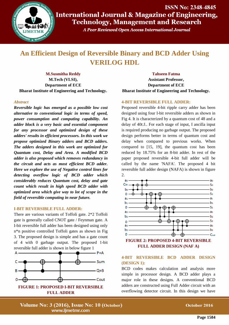
I-BIT REVERSIBLE FULL ADDER:
There are various variants of Toffoli gate. 2*2 Toffoli
gate is generally called CNOT gate / Feynman gate. A
I-bit reversible full adder has been designed using only
n*n positive controlled Toffoli gates as shown in Fig
3. The proposed design is simple and has a gate count
of 4 with 0 garbage output. The proposed 1-bit
reversible full adder is shown in below figure 1
FIGURE 1: PROPOSED I-BIT REVERSIBLE
FULL ADDER
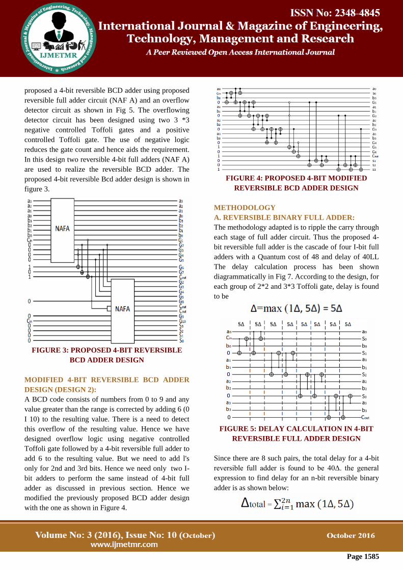
4-BIT REVERSIBLE FULL ADDER:
Proposed reversible 4-bit ripple carry adder has been
designed using four I-bit reversible adders as shown in
Fig 4. It is characterized by a quantum cost of 48 and a
delay of 40t:J.. For each stage of input, I ancilla input
is required producing no garbage output. The proposed
design performs better in terms of quantum cost and
delay when compared to previous works. When
compared to [15, 19], the quantum cost has been
reduced by 18.75% for an 8-bit adder. In rest of the
paper proposed reversible 4-bit full adder will be
called by the name 'NAFA'. The proposed 4 bit
reversible full adder design (NAFA) is shown in figure
2.
FIGURE 2: PROPOSED 4-BIT REVERSIBLE
FULL ADDER DESIGN (NAF A)
4-BIT REVERSIBLE BCD ADDER DESIGN
(DESIGN 1):
BCD codes makes calculation and analysis more
simple in processor design. A BCD adder plays a
major role in these designs. A conventional BCD
adders are constructed using Full Adder circuit with an
overflowing detector circuit. In this design we have
Page 1585
proposed a 4-bit reversible BCD adder using proposed
reversible full adder circuit (NAF A) and an overflow
detector circuit as shown in Fig 5. The overflowing
detector circuit has been designed using two 3 *3
negative controlled Toffoli gates and a positive
controlled Toffoli gate. The use of negative logic
reduces the gate count and hence aids the requirement.
In this design two reversible 4-bit full adders (NAF A)
are used to realize the reversible BCD adder. The
proposed 4-bit reversible Bcd adder design is shown in
figure 3.
FIGURE 3: PROPOSED 4-BIT REVERSIBLE
BCD ADDER DESIGN
MODIFIED 4-BIT REVERSIBLE BCD ADDER
DESIGN (DESIGN 2):
A BCD code consists of numbers from 0 to 9 and any
value greater than the range is corrected by adding 6 (0
I 10) to the resulting value. There is a need to detect
this overflow of the resulting value. Hence we have
designed overflow logic using negative controlled
Toffoli gate followed by a 4-bit reversible full adder to
add 6 to the resulting value. But we need to add l's
only for 2nd and 3rd bits. Hence we need only two I-
bit adders to perform the same instead of 4-bit full
adder as discussed in previous section. Hence we
modified the previously proposed BCD adder design
with the one as shown in Figure 4.
FIGURE 4: PROPOSED 4-BIT MODIFIED
REVERSIBLE BCD ADDER DESIGN
METHODOLOGY
A. REVERSIBLE BINARY FULL ADDER:
The methodology adapted is to ripple the carry through
each stage of full adder circuit. Thus the proposed 4-
bit reversible full adder is the cascade of four I-bit full
adders with a Quantum cost of 48 and delay of 40LL
The delay calculation process has been shown
diagrammatically in Fig 7. According to the design, for
each group of 2*2 and 3*3 Toffoli gate, delay is found
to be
FIGURE 5: DELAY CALCULATION IN 4-BIT
REVERSIBLE FULL ADDER DESIGN
Since there are 8 such pairs, the total delay for a 4-bit
reversible full adder is found to be 40Δ. the general
expression to find delay for an n-bit reversible binary
adder is as shown below:

Page 1586
Reversible BCD Adder:
A binary coded decimal is a form of number system in
which every four bits of a number is represented by its
equivalent value. For example, a decimal number 45 is
represented as 0100 0101 in BCD system. This makes
things simple and facilitates the logic designer to
understand the logic. While designing a combinational
circuit using BCD logic, we may need to perform
different operations on it such as addition, subtraction,
etc. While performing any operation, there may be
chances of overflowing the range of the number
system. In such a case, a detector and corrector circuit
needs to be present. During BCD addition if there is
any overflow, the logic to correct is to add 6 (0 I I 0) to
the resulting data.
The design methodology involves detecting overflow
of the resulting sum from 4-bit reversible full adder
and then adding 6 to it using another 4-bit reversible
full adder. In this proposed design, we have used
cascade of two negative controlled Toffoli and a
positive controlled Toffoli gate to detect the overflow
and have used nother 4-bit reversible binary adder to
correct it by adding 6 (0110) to the output of first full
adder. By this the quantum cost has been found to be
113 with gate count of 35 and delay of 97LL In case of
modified full adder (Design 2), we have removed the
redundancy present in the reversible BCD adder
proposed (Design I) as we need only two I-bit full
adder instead of 4-bit full adder. This will reduce the
delay as well as area.
COMPARISION
Reversible Binary Full Adder:
n-bit reversible binary full adder proposed is
characterized by the quantum cost of 12n, delay of
IOn, 4n ancilla inputs and 0 garbage outputs. When
compared to [15, 19], the quantum cost of the
proposed design has been reduced by 18.75% for an 8-
bit adder. The delay has been improved by 7.5% when
compared to [18]. Table I gives the comparison of n-
bit full reversible binary full adder. Table II gives the
percentage improvement in quantum cost for different
bits.
TABLE 1. COMPARISON OF N-BIT
REVERSIBLE FULL ADDER
TABLE 2: QUANTUM COST COMPARISON OF
N-BIT REVERSIBLE FULL ADDER
REVERSIBLE BCD ADDER:
TABLE 3. COMPARISON OF 4-BIT
REVERSIBLE BCD ADDER
In [14] 6 designs and in [15],4 works on BCD adders
are proposed based on varying parameters such as
Ancilla inputs, garbage outputs, quantum cost and the
delay. Among them, the design with minimum Ancilla
inputs and garbage outputs are compared here.
Page 1587
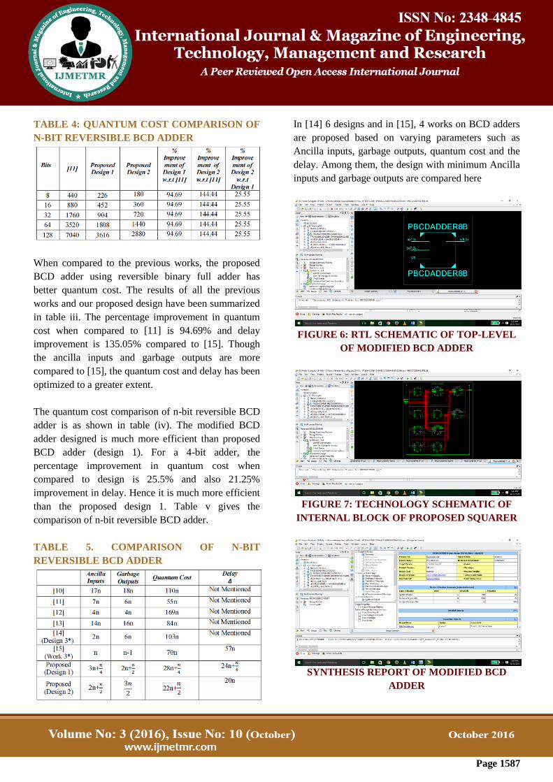
TABLE 4: QUANTUM COST COMPARISON OF
N-BIT REVERSIBLE BCD ADDER
When compared to the previous works, the proposed
BCD adder using reversible binary full adder has
better quantum cost. The results of all the previous
works and our proposed design have been summarized
in table iii. The percentage improvement in quantum
cost when compared to [11] is 94.69% and delay
improvement is 135.05% compared to [15]. Though
the ancilla inputs and garbage outputs are more
compared to [15], the quantum cost and delay has been
optimized to a greater extent.
The quantum cost comparison of n-bit reversible BCD
adder is as shown in table (iv). The modified BCD
adder designed is much more efficient than proposed
BCD adder (design 1). For a 4-bit adder, the
percentage improvement in quantum cost when
compared to design is 25.5% and also 21.25%
improvement in delay. Hence it is much more efficient
than the proposed design 1. Table v gives the
comparison of n-bit reversible BCD adder.
TABLE 5. COMPARISON OF N-BIT
REVERSIBLE BCD ADDER
In [14] 6 designs and in [15], 4 works on BCD adders
are proposed based on varying parameters such as
Ancilla inputs, garbage outputs, quantum cost and the
delay. Among them, the design with minimum Ancilla
inputs and garbage outputs are compared here
FIGURE 6: RTL SCHEMATIC OF TOP-LEVEL
OF MODIFIED BCD ADDER
FIGURE 7: TECHNOLOGY SCHEMATIC OF
INTERNAL BLOCK OF PROPOSED SQUARER
SYNTHESIS REPORT OF MODIFIED BCD
ADDER
Page 1588
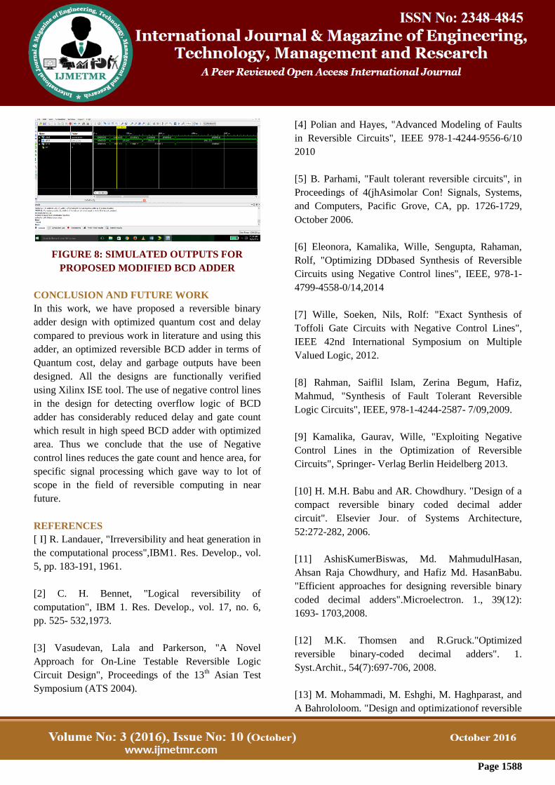
FIGURE 8: SIMULATED OUTPUTS FOR
PROPOSED MODIFIED BCD ADDER
CONCLUSION AND FUTURE WORK
In this work, we have proposed a reversible binary
adder design with optimized quantum cost and delay
compared to previous work in literature and using this
adder, an optimized reversible BCD adder in terms of
Quantum cost, delay and garbage outputs have been
designed. All the designs are functionally verified
using Xilinx ISE tool. The use of negative control lines
in the design for detecting overflow logic of BCD
adder has considerably reduced delay and gate count
which result in high speed BCD adder with optimized
area. Thus we conclude that the use of Negative
control lines reduces the gate count and hence area, for
specific signal processing which gave way to lot of
scope in the field of reversible computing in near
future.
REFERENCES
[ I] R. Landauer, "Irreversibility and heat generation in
the computational process",IBM1. Res. Develop., vol.
5, pp. 183-191, 1961.
[2] C. H. Bennet, "Logical reversibility of
computation", IBM 1. Res. Develop., vol. 17, no. 6,
pp. 525- 532,1973.
[3] Vasudevan, Lala and Parkerson, "A Novel
Approach for On-Line Testable Reversible Logic
Circuit Design", Proceedings of the 13th Asian Test
Symposium (ATS 2004).
[4] Polian and Hayes, "Advanced Modeling of Faults
in Reversible Circuits", IEEE 978-1-4244-9556-6/10
2010
[5] B. Parhami, "Fault tolerant reversible circuits", in
Proceedings of 4(jhAsimolar Con! Signals, Systems,
and Computers, Pacific Grove, CA, pp. 1726-1729,
October 2006.
[6] Eleonora, Kamalika, Wille, Sengupta, Rahaman,
Rolf, "Optimizing DDbased Synthesis of Reversible
Circuits using Negative Control lines", IEEE, 978-1-
4799-4558-0/14,2014
[7] Wille, Soeken, Nils, Rolf: "Exact Synthesis of
Toffoli Gate Circuits with Negative Control Lines",
IEEE 42nd International Symposium on Multiple
Valued Logic, 2012.
[8] Rahman, Saiflil Islam, Zerina Begum, Hafiz,
Mahmud, "Synthesis of Fault Tolerant Reversible
Logic Circuits", IEEE, 978-1-4244-2587- 7/09,2009.
[9] Kamalika, Gaurav, Wille, "Exploiting Negative
Control Lines in the Optimization of Reversible
Circuits", Springer- Verlag Berlin Heidelberg 2013.
[10] H. M.H. Babu and AR. Chowdhury. "Design of a
compact reversible binary coded decimal adder
circuit". Elsevier Jour. of Systems Architecture,
52:272-282, 2006.
[11] AshisKumerBiswas, Md. MahmudulHasan,
Ahsan Raja Chowdhury, and Hafiz Md. HasanBabu.
"Efficient approaches for designing reversible binary
coded decimal adders".Microelectron. 1., 39(12):
1693- 1703,2008.
[12] M.K. Thomsen and R.Gruck."Optimized
reversible binary-coded decimal adders". 1.
Syst.Archit., 54(7):697-706, 2008.
[13] M. Mohammadi, M. Eshghi, M. Haghparast, and
A Bahrololoom. "Design and optimizationof reversible
Page 1589
bcdadderlsubtractor circuit for quantum and
nanotechnology based systems".World Applied
Sciences Journal, 4(6):787-792, 2008.
[14] M. Mohammadi, M. Haghparast, M. Eshghi, and
K. Navi. "Minimization optimization of reversible bcd-
full adderlsubtractor using genetic algorithm and don't
care concept". InternationalJ. Quantum Information,
7(5):969-989, 2009.
[15] HimanshuThapliyal and NagarajanRanganathan,
"Design of Efficient Reversible Logic based Binary
and BCD adder circuits", ACM Journal on Emerging
Technologies in Computing Systems, Vol. 9, Issue 3,
September 2013.
[16] H.R. Bhagyalakshmi and M.K. Venkatesha,
"Optimized reversible BCD adder using new reversible
logic gates", Journal of Computing, Volume 2, Issue 2,
February 2010, ISSN 2151-9617.
[17] Hafiz Md. HasanBabu and Ahsan Raja
Chowdhury, "Design of a Reversible Binary Coded
Decimal Adder by using Reversible 4-bit Parallel
Adder ", Proceedings of the 181h International
Conference on VLSI Design and 4th International
Conference on Embedded Systems Design, 1063-
9667/05, IEEE 2005.
[18] K. V. R. M. Murali, N. Sinha, T. S. Mahesh, M.
H. Levitt, K. V. Ramanathan, and A Kumar."Quantum
information processing by nuclear magnetic resonance:
experimental implementation of half-adder and
subtractor operations using an oriented spin"-7/2
system. Physical Review A, 66(2):022313, 2002.
[19] Kai-Wen Cheng and Chien-Cheng Tseng.
"Quantum full adder and
subtractor".ElectronicsLetters, 38(22): 1343- 1344,
Oct 2002.