design and implementation of a unified bcd/binary adder/subtractor
TRANSCRIPT
Chapter 5 Design and Implementation of a Unified
BCD/Binary Adder/Subtractor
Contents Chapter 5 ............................................................................................................................... 74
5.1 Introduction ............................................................................................................... 74
5.2 Review of Existing Techniques for BCD Addition/Subtraction ............................... 76
5.2.1 One-Digit BCD Full Adder ..............................................................................76
5.2.2 Higher Bit BCD/Binary Adders/Subtractors ....................................................77
5.3 A Unified BCD/Binary Adder/Subtractor Architecture ............................................ 79
5.3.1 Conventional Binary Adder /Subtractor ...........................................................80
5.3.2 A Modified Binary Adder/Subtractor ...............................................................82
5.3.3 Modified BCD Adder/Subtractor .....................................................................84
5.3.4 A Modified Unified BCD/Binary Adder/Subtractor Architecture ...................88
5.4 Simulations and Results ............................................................................................ 89
5.5 Conclusions ............................................................................................................... 92
5.1 Introduction
There is a growing importance of decimal arithmetic in commercial, financial and internet-
based applications. These applications cannot tolerate errors that result from the conversion of
binary format to decimal format. Thus, hardware support for decimal arithmetic is receiving
considerable attention. Recently, specifications for decimal floating point arithmetic have been
added to the draft revision of IEEE-754 standard for floating point arithmetic [43]. Despite the
widespread use of binary arithmetic, decimal computation remains essential for many
applications. Not only is it required whenever numbers are presented for human inspection, but is
also often a necessity when fractions are involved. Decimal fractions are pervasive in human
endeavors, yet most cannot be represented by binary fractions. The value 0.1 for example,
5.1 Introduction
75
requires an infinitely recurring binary number. If a binary approximation is used instead of an
exact decimal fraction, results can be incorrect even if subsequent arithmetic is correct.
As the IEEE standard for decimal floating point is approved, hardware support for decimal
floating point arithmetic will be incorporated in processors for various applications. Still, a major
consideration while implementing Binary Coded Decimal (BCD) arithmetic is to enhance its
speed as much as possible.
BCD is a decimal representation of a number directly coded in binary, digit by digit. For
example, the number (9527)10 is represented as (1001 0101 0010 0111)BCD . It can be seen that
each digit of the decimal number is coded in binary and then concatenated to form BCD
representation of the decimal number.
To use this representation all the arithmetic and logical operations need to be defined. As
the decimal number system contains 10 digits, at least 4 bits are needed to represent a BCD digit.
The BCD representation of digit A is A4A3A2A1 where all ( )1,0∈kA . The only point to note is
that the maximum value that can be represented by a BCD digit is ‘9’. The representation of
(10)10 in BCD is (0001 0000).
Addition in BCD can be explained by considering two decimal digits A and B with BCD
representations as A4A3A2A1 and B4B3B2B1 respectively. In the conventional approach , these
two numbers are added using a 4-bit binary adder during which it is possible that the resultant
Sum can exceed 9 resulting in an overflow. If the Sum is greater than 9, the binary equivalent of
6 is added to the resultant Sum to obtain the exact BCD representation. This can be illustrated
with the following example
)00010001()11(00011
)6(0110)11(1011
)5(0101)6(0110
=AnswerBCDinBCD
AddSumBA
5.2 Review of Existing Techniques for BCD Addition/Subtraction
76
5.2 Review of Existing Techniques for BCD Addition/Subtraction
5.2.1 One-Digit BCD Full Adder
A BCD 1-digit adder is a circuit that adds two BCD digits in parallel and also produces the
Sum digit in BCD along with the necessary correction logic. The conventional implementation of
addition as mentioned above is shown in Fig 5.1[44]. It can be seen that a 4-bit binary adder is
used initially to add two BCD digits (each digit expressed using 4 bits) with a carry-input. An
overflow detection circuit is used (to check if the ‘Sum’ of the BCD digit has exceeded 9) which
is designed using two 2-input AND gates and a 3-input OR gate. Finally, another 4-bit binary
adder is used as a correction stage, which comes in the path of final Sum computation. Thus, the
critical path in this circuit consists of a 4-bit binary adder, overflow logic and one more 4-bit
binary adder. Assuming, in the best case, that the 4-bit binary adder is a carry look-ahead adder,
a gate level analysis would indicate that it consists of 4-gates in the critical path. It can be
observed from Fig 5.1 that the overflow detection circuit comes into picture only after the top-
most 4-bit binary adder performs its operation and it consists of 2 gates in the critical path. Thus,
a minimum of a 10-gate delay can be expected in conventional implementation [44]. The above
design can however be optimized by removing those gates that are completely redundant in their
operation. Such a modification is shown in Fig 5.2 which results in a smaller critical path. A
faster carry prediction for this implementation is proposed in [45], which uses carry look-ahead
logic to predict the carry in advance. These 1-digit full adders can be cascaded to realize higher
digit BCD adders.
Figure 5.1 Block Diagram of Conventional 1-digit BCD Full Adder
5.2 Review of Existing Techniques for BCD Addition/Subtraction
77
Figure 5.2 Block Diagram of Modified Conventional 1-digit BCD FA
5.2.2 Higher Bit BCD/Binary Adders/Subtractors
A unified BCD/Binary module is the one, which can perform both BCD as well as binary
operation. There have been many contributions on decimal arithmetic especially on
adders/subtractors [43-56]. Some of the initial contributions came from Schoomklar et al. [46]
and Adiletta et al. [47]. The first BCD sign-magnitude adder/subtractor was designed by Grupe
[48]. An area efficient sign-magnitude adder was later developed by Hwang [49]. In this
approach two additional conversions were introduced before and after the binary addition.
A BCD adder similar to the carry select adder was presented in [50]. This design
concurrently calculates two results, one assuming the presence of the input carry and the other its
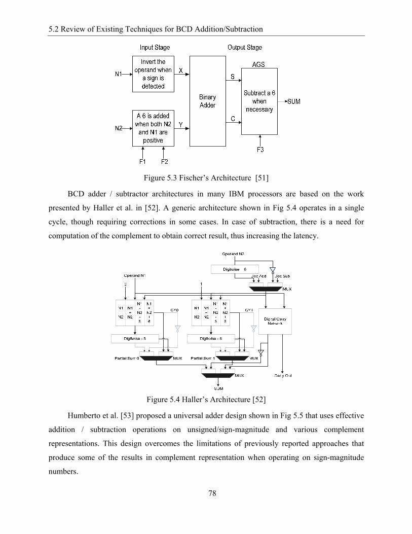
absence. It then selects the appropriate result as the carry is computed. Fischer et al. [51] later
came up with an improved version of this design shown in Fig 5.3 where only a single adder was
used to reduce the area overhead.
F A F A F A F A
F A F A
Cin
A 3 A 2 A 1 A 0 B 3 B 2 B 1 B 0
Cout S 3 S 2 S 1 S 0
0
CO CI
S
CO CI
S
CO CI
S
CO CI
S
CO CI
S
CO CI
S
1 1XX A1
A2 1X1X
5.2 Review of Existing Techniques for BCD Addition/Subtraction
78
Figure 5.3 Fischer’s Architecture [51]
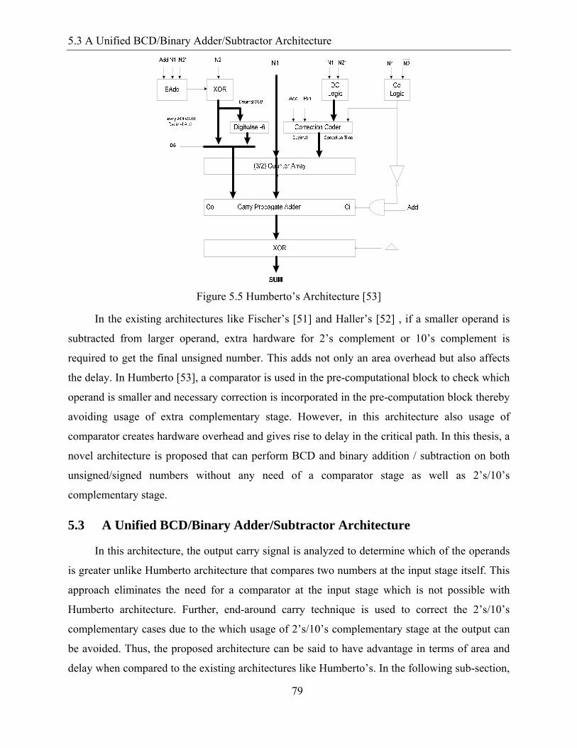
BCD adder / subtractor architectures in many IBM processors are based on the work
presented by Haller et al. in [52]. A generic architecture shown in Fig 5.4 operates in a single
cycle, though requiring corrections in some cases. In case of subtraction, there is a need for
computation of the complement to obtain correct result, thus increasing the latency.
Figure 5.4 Haller’s Architecture [52]
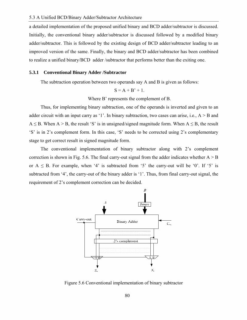
Humberto et al. [53] proposed a universal adder design shown in Fig 5.5 that uses effective
addition / subtraction operations on unsigned/sign-magnitude and various complement
representations. This design overcomes the limitations of previously reported approaches that
produce some of the results in complement representation when operating on sign-magnitude
numbers.
5.3 A Unified BCD/Binary Adder/Subtractor Architecture
79
Figure 5.5 Humberto’s Architecture [53]
In the existing architectures like Fischer’s [51] and Haller’s [52] , if a smaller operand is
subtracted from larger operand, extra hardware for 2’s complement or 10’s complement is
required to get the final unsigned number. This adds not only an area overhead but also affects
the delay. In Humberto [53], a comparator is used in the pre-computational block to check which
operand is smaller and necessary correction is incorporated in the pre-computation block thereby
avoiding usage of extra complementary stage. However, in this architecture also usage of
comparator creates hardware overhead and gives rise to delay in the critical path. In this thesis, a
novel architecture is proposed that can perform BCD and binary addition / subtraction on both
unsigned/signed numbers without any need of a comparator stage as well as 2’s/10’s
complementary stage.
5.3 A Unified BCD/Binary Adder/Subtractor Architecture
In this architecture, the output carry signal is analyzed to determine which of the operands
is greater unlike Humberto architecture that compares two numbers at the input stage itself. This
approach eliminates the need for a comparator at the input stage which is not possible with
Humberto architecture. Further, end-around carry technique is used to correct the 2’s/10’s
complementary cases due to the which usage of 2’s/10’s complementary stage at the output can
be avoided. Thus, the proposed architecture can be said to have advantage in terms of area and
delay when compared to the existing architectures like Humberto’s. In the following sub-section,
5.3 A Unified BCD/Binary Adder/Subtractor Architecture
80
a detailed implementation of the proposed unified binary and BCD adder/subtractor is discussed.
Initially, the conventional binary adder/subtractor is discussed followed by a modified binary
adder/subtractor. This is followed by the existing design of BCD adder/subtractor leading to an
improved version of the same. Finally, the binary and BCD adder/subtractor has been combined
to realize a unified binary/BCD adder /subtractor that performs better than the exiting one.
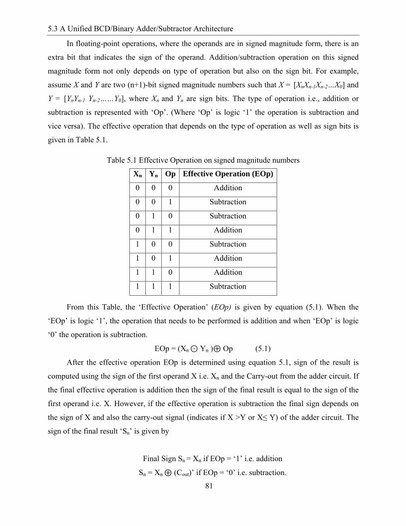
5.3.1 Conventional Binary Adder /Subtractor
The subtraction operation between two operands say A and B is given as follows:
S = A + B’ + 1.
Where B’ represents the complement of B.
Thus, for implementing binary subtraction, one of the operands is inverted and given to an
adder circuit with an input carry as ‘1’. In binary subtraction, two cases can arise, i.e., A > B and
A ≤ B. When A > B, the result ‘S’ is in unsigned/signed magnitude form. When A ≤ B, the result
‘S’ is in 2’s complement form. In this case, ‘S’ needs to be corrected using 2’s complementary
stage to get correct result in signed magnitude form.
The conventional implementation of binary subtractor along with 2’s complement
correction is shown in Fig. 5.6. The final carry-out signal from the adder indicates whether A > B
or A ≤ B. For example, when ‘4’ is subtracted from ‘5’ the carry-out will be ‘0’. If ‘5’ is
subtracted from ‘4’, the carry-out of the binary adder is ‘1’. Thus, from final carry-out signal, the
requirement of 2’s complement correction can be decided.
Figure 5.6 Conventional implementation of binary subtractor
5.3 A Unified BCD/Binary Adder/Subtractor Architecture
81
In floating-point operations, where the operands are in signed magnitude form, there is an
extra bit that indicates the sign of the operand. Addition/subtraction operation on this signed
magnitude form not only depends on type of operation but also on the sign bit. For example,
assume X and Y are two (n+1)-bit signed magnitude numbers such that X = [XnXn-1Xn-2…X0] and
Y = [YnYn-1 Yn-2……Y0], where Xn and Yn are sign bits. The type of operation i.e., addition or
subtraction is represented with ‘Op’. (Where ‘Op’ is logic ‘1’ the operation is subtraction and
vice versa). The effective operation that depends on the type of operation as well as sign bits is
given in Table 5.1.
Table 5.1 Effective Operation on signed magnitude numbers
Xn Yn Op Effective Operation (EOp)
0 0 0 Addition
0 0 1 Subtraction
0 1 0 Subtraction
0 1 1 Addition
1 0 0 Subtraction
1 0 1 Addition
1 1 0 Addition
1 1 1 Subtraction
From this Table, the ‘Effective Operation’ (EOp) is given by equation (5.1). When the
‘EOp’ is logic ‘1’, the operation that needs to be performed is addition and when ‘EOp’ is logic
‘0’ the operation is subtraction.
EOp = (Xn Yn ) Op (5.1)
After the effective operation EOp is determined using equation 5.1, sign of the result is
computed using the sign of the first operand X i.e. Xn and the Carry-out from the adder circuit. If
the final effective operation is addition then the sign of the final result is equal to the sign of the
first operand i.e. X. However, if the effective operation is subtraction the final sign depends on
the sign of X and also the carry-out signal (indicates if X >Y or X≤ Y) of the adder circuit. The
sign of the final result ‘Sn’ is given by
Final Sign Sn = Xn if EOp = ‘1’ i.e. addition
Sn = Xn (Cout)’ if EOp = ‘0’ i.e. subtraction.

5.3 A Unified BCD/Binary Adder/Subtractor Architecture
82
The sign of final result from the above equation can be obtained using the implementation
shown in the Fig 5.7
Figure 5.7 Final Sign ‘Sn’ computation logic
The design of binary adder/subtractor with conventional subtractor explained earlier and
which supports the signed magnitude form is shown in Fig 5.8. From the figure, it can be
observed that the extra 2’s complementary stage increases delay and area when compared to the
same used for addition operation.
Figure 5.8 Conventional implementation of binary adder/subtractor with signed magnitude
5.3.2 A Modified Binary Adder/Subtractor
In this section, a binary adder/subtractor is proposed which uses end-around carry method
to eliminate the complementary correction stage. For using end-around carry method, the adder
5.3 A Unified BCD/Binary Adder/Subtractor Architecture
83
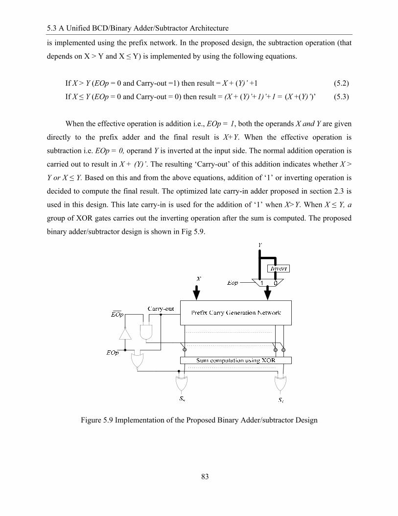
is implemented using the prefix network. In the proposed design, the subtraction operation (that
depends on X > Y and X ≤ Y) is implemented by using the following equations.
If X > Y (EOp = 0 and Carry-out =1) then result = X + (Y)’ +1 (5.2)
If X ≤ Y (EOp = 0 and Carry-out = 0) then result = (X + (Y)’+1)’+1 = (X +(Y)’)’ (5.3)
When the effective operation is addition i.e., EOp = 1, both the operands X and Y are given
directly to the prefix adder and the final result is X+Y. When the effective operation is
subtraction i.e. EOp = 0, operand Y is inverted at the input side. The normal addition operation is
carried out to result in X + (Y)’. The resulting ‘Carry-out’ of this addition indicates whether X >
Y or X ≤ Y. Based on this and from the above equations, addition of ‘1’ or inverting operation is
decided to compute the final result. The optimized late carry-in adder proposed in section 2.3 is
used in this design. This late carry-in is used for the addition of ‘1’ when X>Y. When X ≤ Y, a
group of XOR gates carries out the inverting operation after the sum is computed. The proposed
binary adder/subtractor design is shown in Fig 5.9.
Figure 5.9 Implementation of the Proposed Binary Adder/subtractor Design
5.3 A Unified BCD/Binary Adder/Subtractor Architecture
84
5.3.3 Modified BCD Adder/Subtractor
The existing BCD Adder/Subtractor architectures and the limitations of the same have
been explained in section 5.2. In this section, a modified BCD adder/subtractor architecture is
presented which overcomes these limitations. The proposed design is inspired from Fischer
approach but eliminates the usage of complementary stage as well as supports unsigned and
signed magnitude form.
In Fischer’s approach, the BCD addition operation is performed by pre-correction block
where digit-wise addition of ‘6’ is carried out for one of the operands. After pre-correction the
result is added to other operand by a binary adder. The post-correction block includes conditional
subtraction of ‘6’ depending up on the ‘Carry-out’ at each digit stage. This signal at each digit
stage indicates whether the digit is greater than ‘9’ or not. For example, if the ‘Carry-out’ is ‘1’
the digit is less than or equal to ‘9’ and hence no correction is required. If the ‘Carry-out’ is ‘0’
the digit is greater than ‘9’ and a correction by subtraction of ‘6’ is needed. Since 2’s
complement of ‘6’ is ‘10’, subtraction of ‘6’ i.e. (0110)2 is accomplished by addition of ‘10’ i.e.,
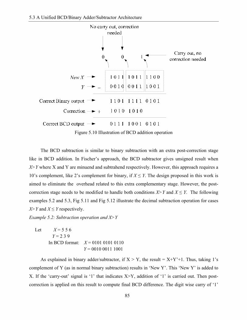
(1010)2. The following example 5.1 and Fig 5.10 illustrate the above decimal addition operation.
Example 5.1:
Let X = 5 5 6
Y = 2 3 9
In BCD format: X = 0101 0101 0110
Y = 0010 0011 1001
Addition of digit-wise 6 i.e. (0110)2 to X results in new X,
X = 0101 0101 0110
+6 0110 0110 0110
Hence, new X = 1011 1011 1100
Now the ‘new X’ is added to Y and correction is applied.
5.3 A Unified BCD/Binary Adder/Subtractor Architecture
85
Figure 5.10 Illustration of BCD addition operation
The BCD subtraction is similar to binary subtraction with an extra post-correction stage
like in BCD addition. In Fischer’s approach, the BCD subtractor gives unsigned result when
X>Y where X and Y are minuend and subtrahend respectively. However, this approach requires a
10’s complement, like 2’s complement for binary, if X ≤ Y. The design proposed in this work is
aimed to eliminate the overhead related to this extra complementary stage. However, the post-
correction stage needs to be modified to handle both conditions X>Y and X ≤ Y. The following
examples 5.2 and 5.3, Fig 5.11 and Fig 5.12 illustrate the decimal subtraction operation for cases
X>Y and X ≤ Y respectively.
Example 5.2: Subtraction operation and X>Y
Let X = 5 5 6 Y = 2 3 9 In BCD format: X = 0101 0101 0110 Y = 0010 0011 1001
As explained in binary adder/subtractor, if X > Y, the result = X+Y’+1. Thus, taking 1’s
complement of Y (as in normal binary subtraction) results in ‘New Y’. This ‘New Y’ is added to
X. If the ‘carry-out’ signal is ‘1’ that indicates X>Y, addition of ‘1’ is carried out. Then post-
correction is applied on this result to compute final BCD difference. The digit wise carry of ‘1’
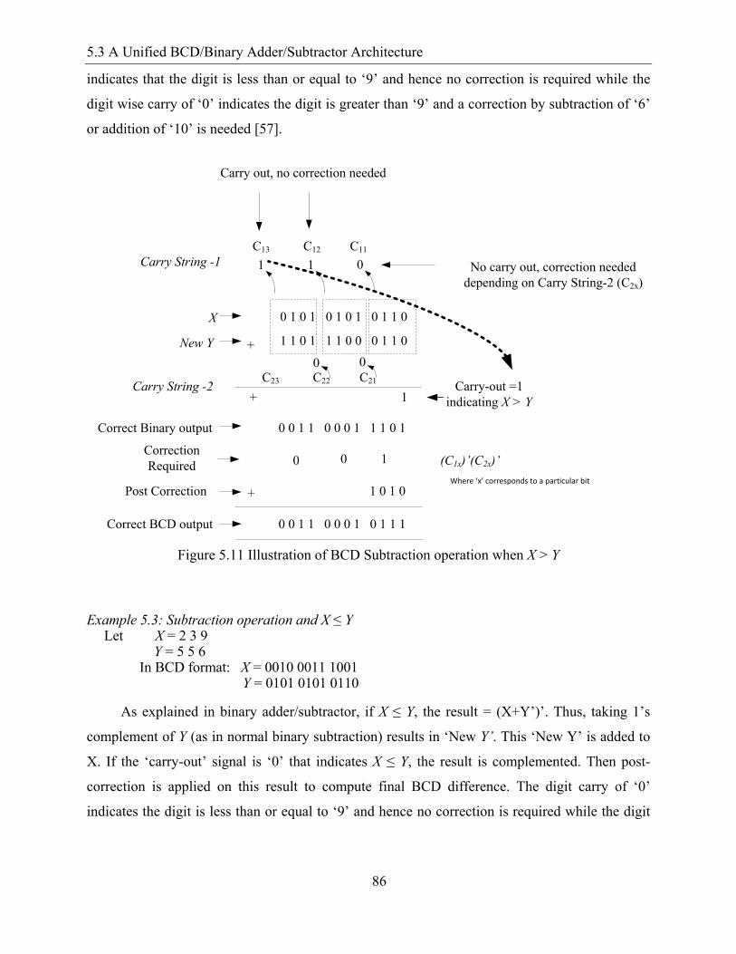
5.3 A Unified BCD/Binary Adder/Subtractor Architecture
86
indicates that the digit is less than or equal to ‘9’ and hence no correction is required while the
digit wise carry of ‘0’ indicates the digit is greater than ‘9’ and a correction by subtraction of ‘6’
or addition of ‘10’ is needed [57].
Correct Binary output
0 1 0 1 0 1 0 1 0 1 1 0
1 1 0 1 1 1 0 0 0 1 1 0+
X
New Y
0 0 1 1 0 0 0 1 1 1 0 1
011 No carry out, correction needed depending on Carry String-2 (C2x)
1 0 1 0
0 0 1 1 0 0 0 1 0 1 1 1
+
Correct BCD output
Post Correction
Carry-out =1 indicating X > Y1
Carry String -1
Carry String -2
00
CorrectionRequired (C1x)’(C2x)’0 10
+
C13 C12 C11
C23 C22 C21
Where ‘x’ corresponds to a particular bit
Carry out, no correction needed
Figure 5.11 Illustration of BCD Subtraction operation when X > Y
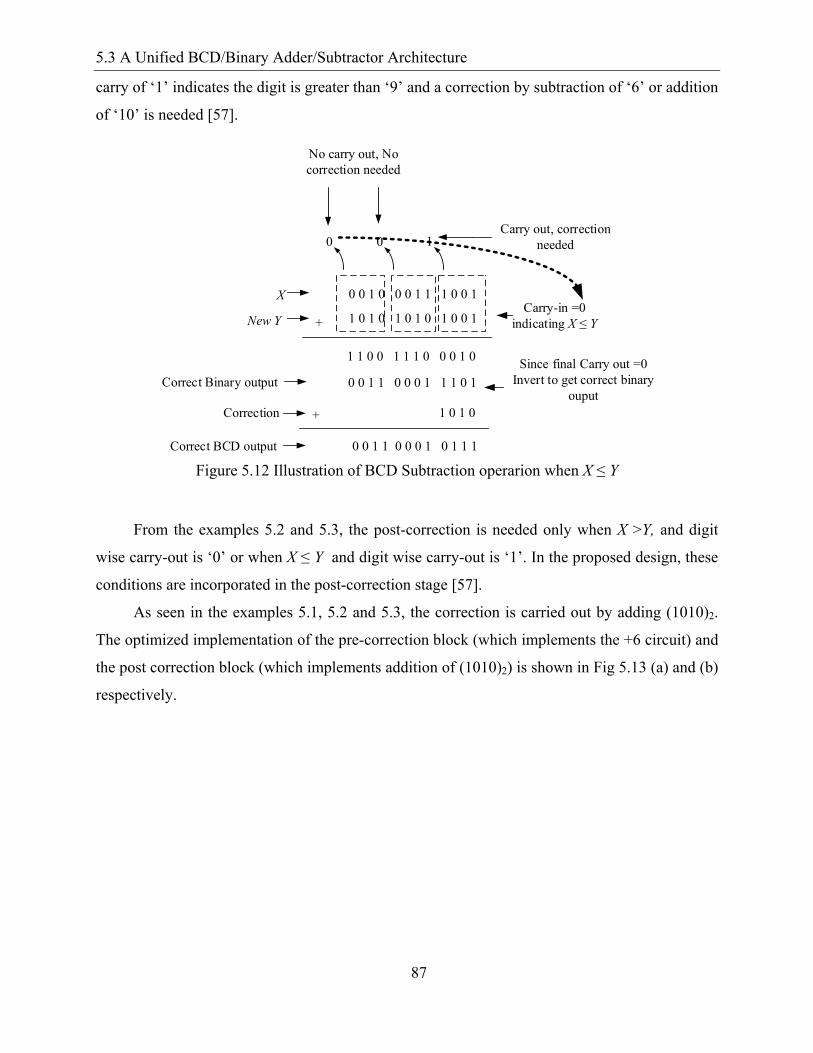
Example 5.3: Subtraction operation and X ≤ Y Let X = 2 3 9 Y = 5 5 6 In BCD format: X = 0010 0011 1001 Y = 0101 0101 0110
As explained in binary adder/subtractor, if X ≤ Y, the result = (X+Y’)’. Thus, taking 1’s
complement of Y (as in normal binary subtraction) results in ‘New Y’. This ‘New Y’ is added to
X. If the ‘carry-out’ signal is ‘0’ that indicates X ≤ Y, the result is complemented. Then post-
correction is applied on this result to compute final BCD difference. The digit carry of ‘0’
indicates the digit is less than or equal to ‘9’ and hence no correction is required while the digit
5.3 A Unified BCD/Binary Adder/Subtractor Architecture
87
carry of ‘1’ indicates the digit is greater than ‘9’ and a correction by subtraction of ‘6’ or addition
of ‘10’ is needed [57].
0 0 1 0 0 0 1 1 1 0 0 1
1 0 1 0 1 0 1 0 1 0 0 1+
X
New Y
1 1 0 0 1 1 1 0 0 0 1 0
100
No carry out, No correction needed
Carry out, correction needed
1 0 1 0
0 0 1 1 0 0 0 1 0 1 1 1
+
Correct Binary output
Correct BCD output
Correction
Carry-in =0 indicating X ≤ Y
0 0 1 1 0 0 0 1 1 1 0 1Since final Carry out =0
Invert to get correct binary ouput
Figure 5.12 Illustration of BCD Subtraction operarion when X ≤ Y
From the examples 5.2 and 5.3, the post-correction is needed only when X >Y, and digit
wise carry-out is ‘0’ or when X ≤ Y and digit wise carry-out is ‘1’. In the proposed design, these
conditions are incorporated in the post-correction stage [57].
As seen in the examples 5.1, 5.2 and 5.3, the correction is carried out by adding (1010)2.
The optimized implementation of the pre-correction block (which implements the +6 circuit) and
the post correction block (which implements addition of (1010)2) is shown in Fig 5.13 (a) and (b)
respectively.
5.3 A Unified BCD/Binary Adder/Subtractor Architecture
88
(a) (b)
Figure 5.13 (a) Pre-correction block (b) Post Correction block for BCD
The control signal for the pre-correction circuit is given as
Cnt1 = EOp. (Bin)’
which indicates that the addition of (0110)2 is activated only for BCD addition operation.
Similarly, the control signal for post correction block is given as
Cnt2 = ((Carry-out + EOp) C4 . Bin ’ Where C4 (C1x)’(C2x)’as shown in the figure 5.11
which indicates the operation as BCD subtraction. It also takes into consideration both the
cases of X >Y and X ≤ Y and also carry out at each digit stage [57].
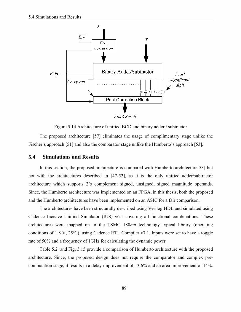
5.3.4 A Modified Unified BCD/Binary Adder/Subtractor Architecture
The proposed unified BCD/Binary adder/subtractor architecture including pre-correction
and post-correction stage is shown in Fig. 5.14. The ‘Bin’ signal indicates whether the operation
is binary or BCD. If Bin =1 indicates binary operation and Bin = 0 indicates BCD operation [57].
5.4 Simulations and Results
89
Figure 5.14 Architecture of unified BCD and binary adder / subtractor
The proposed architecture [57] eliminates the usage of complimentary stage unlike the
Fischer’s approach [51] and also the comparator stage unlike the Humberto’s approach [53].
5.4 Simulations and Results
In this section, the proposed architecture is compared with Humberto architecture[53] but
not with the architectures described in [47-52], as it is the only unified adder/subtractor
architecture which supports 2’s complement signed, unsigned, signed magnitude operands.
Since, the Humberto architecture was implemented on an FPGA, in this thesis, both the proposed
and the Humberto architectures have been implemented on an ASIC for a fair comparison.
The architectures have been structurally described using Verilog HDL and simulated using
Cadence Incisive Unified Simulator (IUS) v6.1 covering all functional combinations. These
architectures were mapped on to the TSMC 180nm technology typical library (operating
conditions of 1.8 V, 25ºC), using Cadence RTL Compiler v7.1. Inputs were set to have a toggle
rate of 50% and a frequency of 1GHz for calculating the dynamic power.
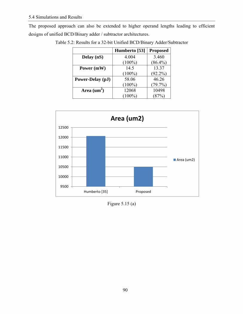
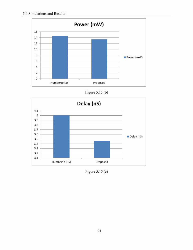
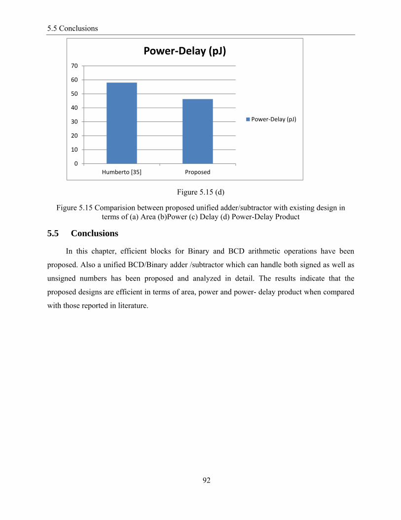
Table 5.2 and Fig. 5.15 provide a comparison of Humberto architecture with the proposed
architecture. Since, the proposed design does not require the comparator and complex pre-
computation stage, it results in a delay improvement of 13.6% and an area improvement of 14%.
5.4 Simulations and Results
90
The proposed approach can also be extended to higher operand lengths leading to efficient
designs of unified BCD/Binary adder / subtractor architectures.
Table 5.2: Results for a 32-bit Unified BCD/Binary Adder/Subtractor
Humberto [53] ProposedDelay (nS) 4.004
(100%) 3.460
(86.4%) Power (mW) 14.5
(100%) 13.37
(92.2%) Power-Delay (pJ) 58.06
(100%) 46.26
(79.7%) Area (um2) 12068
(100%) 10498 (87%)
Figure 5.15 (a)
9500
10000
10500
11000
11500
12000
12500
Humberto [35] Proposed
Area (um2)
Area (um2)
5.4 Simulations and Results
91
Figure 5.15 (b)
Figure 5.15 (c)
0
2
4
6
8
10
12
14
16
Humberto [35] Proposed
Power (mW)
Power (mW)
3.1
3.2
3.3
3.4
3.5
3.6
3.7
3.8
3.9
4
4.1
Humberto [35] Proposed
Delay (nS)
Delay (nS)
5.5 Conclusions
92
Figure 5.15 (d)
Figure 5.15 Comparision between proposed unified adder/subtractor with existing design in terms of (a) Area (b)Power (c) Delay (d) Power-Delay Product
5.5 Conclusions
In this chapter, efficient blocks for Binary and BCD arithmetic operations have been
proposed. Also a unified BCD/Binary adder /subtractor which can handle both signed as well as
unsigned numbers has been proposed and analyzed in detail. The results indicate that the
proposed designs are efficient in terms of area, power and power- delay product when compared
with those reported in literature.
0
10
20
30
40
50
60
70
Humberto [35] Proposed
Power‐Delay (pJ)
Power‐Delay (pJ)