a 15 gsa/s, 1.5 ghz bandwidth waveform digitizing asic · a 15 gsa/s, 1.5 ghz bandwidth waveform...
TRANSCRIPT
A 15 GSa/s, 1.5 GHz Bandwidth Waveform Digitizing ASIC
Eric Oberlaa,∗, Jean-Francois Genata,1, Herve Grabasa,2, Henry Frischa, Kurtis Nishimurab,3, Gary Varnerb
aEnrico Fermi Institute, University of Chicago; 5640 S. Ellis Ave., Chicago IL, 60637bUniversity of Hawai’i at Manoa; Watanabe Hall, 2505 Correa Rd., Honolulu HA
Abstract
The PSEC4 custom integrated circuit was designed for the recording of fast waveforms for use in large-
area time-of-flight detector systems. The ASIC has been fabricated using the IBM-8RF 0.13 µm CMOS
process. On each of 6 analog channels, PSEC4 employs a switched capacitor array (SCA) 256 samples deep,
a ramp-compare ADC with 10.5 bits of DC dynamic range, and a serial data readout with the capability
of region-of-interest windowing to reduce dead time. The sampling rate can be adjusted between 4 and
15 Gigasamples/second [GSa/s] on all channels and is servo-controlled on-chip with a low-jitter delay-locked
loop (DLL). The input signals are passively coupled on-chip with a -3 dB analog bandwidth of 1.5 GHz.
The power consumption in quiescent sampling mode is less than 50 mW/chip; at a sustained trigger and
readout rate of 50 kHz the chip draws 100 mW. After fixed-pattern pedestal subtraction, the uncorrected
integral non-linearity is 0.15% over an 750 mV dynamic range. With a linearity correction, a full 1 V signal
voltage range is available. The sampling timebase has a fixed-pattern non-linearity with an RMS of 13%,
which can be corrected for precision waveform feature extraction and timing.
Keywords:
Waveform sampling, ASIC, Integrated Circuit, Analog-to-Digital, Switched Capacitor Array,
Time-of-Flight
1. Introduction
We describe the design and performance of PSEC4, a ≥10 Gigasample/second [GSa/s] waveform sam-
pling and digitizing Application Specific Integrated Circuit (ASIC) fabricated in the IBM-8RF 0.13 µm
complementary metal-oxide-semiconductor (CMOS) technology. This compact ‘oscilloscope-on-a-chip’ is
designed for the recording of radio-frequency (RF) transient waveforms with signal bandwidths between
100 MHz and 1.5 GHz.
1.1. Background
The detection of discrete photons and high-energy particles is the basis of a wide range of commercial
and scientific applications. In many of these applications, the relative arrival time of an incident photon
∗Corresponding authorEmail address: [email protected] (Eric Oberla)
1Present address, LPNHE, CNRS/IN2P3, Universites Pierre et Marie Curie and Denis Diderot, T12 RC, 4 Place Jussieu75252 Paris CEDEX 05, France
2Present address, CEA/IRFU/SEDI; CEN Saclay-Bat141 F-91191 Gif-sur-Yvette CEDEX, France3Present address, SLAC National Accelerator Laboratory, 2575 Sand Hill Road, Menlo Park, CA 94025
Preprint submitted to elsevier September 18, 2013
arX
iv:1
309.
4397
v1 [
phys
ics.
ins-
det]
17
Sep
2013
or particle is best measured by extracting features from the full waveform at the detector output [1, 2].
Additional benefits of front-end waveform sampling include the detection of pile-up events and the ability
to filter noise or poorly formed pulses.
For recording ‘snapshots’ of transient waveforms, switched capacitor array (SCA) analog memories can
be used to sample a limited time-window at a relatively high rate, but with a latency-cost of a slower readout
speed [3, 4]. These devices are well suited for triggered-event applications, as in many high energy physics
experiments, in which some dead-time on each channel is acceptable. With modern CMOS integrated circuit
design, these SCA sampling chips can be compact, low power, and have a relatively low cost per channel [4].
Over the last decade, sampling rates in SCA waveform sampling ASICs have been pushed to several
GSa/s with analog bandwidths of several hundred MHz up to ∼1 GHz [5, 6]. As a scalable front-end
readout option coupled with the advantages of waveform sampling, these ASICs have been used in a wide
range of experiments; such as high-energy physics colliders [6], gamma-ray astronomy [7, 8], high-energy
neutrino detection [9, 10], and rare decay searches [11, 12].
1.2. Motivation
A natural extension to the existing waveform sampling ASICs is to push design parameters that are
inherently fabrication-technology limited. Parameters such as sampling rate and analog bandwidth are of
particular interest considering the fast risetimes (τ r ∼ 60 - 500 ps) and pulse widths (FWHM ∼ 200 ps - 1 ns)
of commercially available and novel technologies of micro-channel plate (MCP) and silicon photomultipli-
ers [13, 14, 15]. These and other fast photo-optical or RF devices require electronics matched to the speed
of the signals.
The timing resolution of discrete waveform sampling is intuitively dependent on three primary factors
as described by Ritt4 [16]:
σt ∝τr
(SNR)√Nsamples
(1)
where SNR is the signal-to-noise ratio of the pulse, τ r is the 10-90% rise-time of the pulse, and Nsamples
is the number of independent samples on the rising edge within time τ r. The motivation for oversampling
above the Nyquist limit is that errors due to uncorrelated noise, caused both by random time jitter and
charge fluctuations, are reduced by increasing the rising-edge sample size. Accordingly, in order to preserve
the timing properties of analog signals from a fast detector, the waveform recording electronics should 1) be
low-noise, 2) match the signal bandwidth, and 3) have a fast sampling rate relative to the signal rise-time.
1.3. Towards 0.13 µm CMOS
The well-known advantages of reduced transistor feature size include higher clock speeds, greater circuit
density, lower parasitic capacitances, and lower power dissipation per circuit [17]. The sampling rate and
analog bandwidth of waveform sampling ASICs, which depend on clock speeds, parasitic capacitances, and
interconnect lengths, are directly enhanced by moving to a smaller CMOS technology. Designing in a smaller
technology also allows clocking of an on-chip analog-to-digital converter (ADC) at a faster rate, reducing
the chip dead-time.
With the advantages of reduced transistor feature sizes also comes increasingly challenging analog design
issues. One issue is the increase of leakage current. Leakage is enhanced by decreased source-drain channel
4Assuming Shannon-Nyquist is fulfilled
2
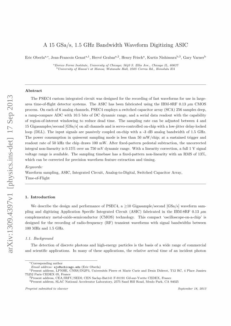
Figure 1: The fabricated PSEC4 chip. The die dimensions are 4×4.2 mm2.
lengths, causing subthreshold leakage (VGS < VTH), and decreased gate-oxide thickness, which promotes
gate-oxide tunneling [18]. Effects of leakage include increased quiescent power dissipation and potential
non-linear effects when storing analog voltages.
Another design issue of deeper sub-micron technologies is the reduced dynamic range [18]. The available
voltage range is given by (VDD-VTH), where VDD is the supply voltage and VTH is the threshold, or ‘turn-
on’, voltage for a given transistor. For technologies above 0.1 µm, the (VDD-VTH) range is decreased with
downscaled feature sizes to reduce high-field effects in the gate-oxide [18]. In the 0.13 µm CMOS process,
the supply voltage VDD is 1.2 V and the values of VTH range from 0.42 V for a minimum-size transistor
(gate length 120 nm) to roughly 0.2 V for a large transistor (5 µm) [19, 20].
The potential of waveform sampling design in 0.13 µm CMOS was shown with two previous ASICs. A
waveform sampling prototype, PSEC3, achieved a sampling rate of 15 GSa/s and showed the possibility of
analog bandwidths above 1 GHz [21]. Leakage and dynamic range studies were also performed with this
chip. In a separate 0.13 µm ASIC, fabricated as a test-structure chip called CHAMP, a 25 GSa/s sampling
rate rate was achieved using low VTH transistors [22]. The performance and limitations of these chips led
to the optimized design of the PSEC4 waveform digitizing ASIC. The fabricated PSEC4 die is shown in
Figure 1.
In this paper, we describe the PSEC4 architecture (§2), and experimental performance (§3).
2. Architecture
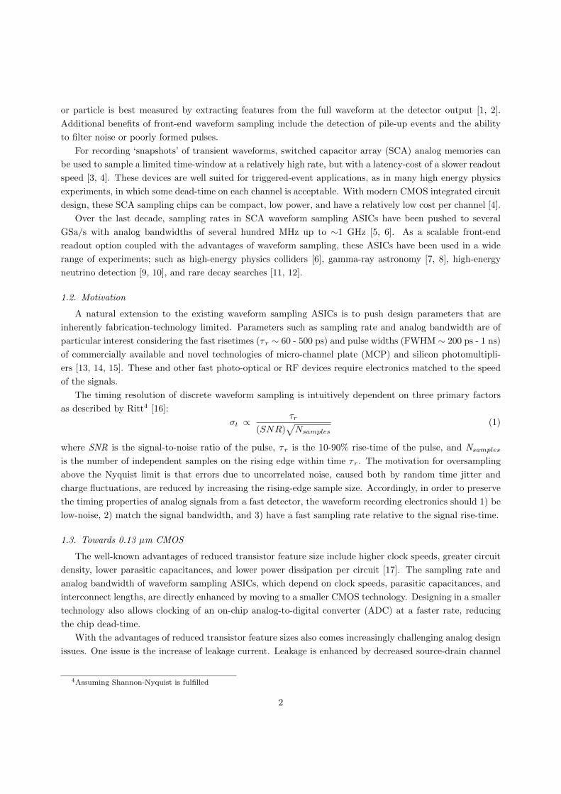
An overview of the PSEC4 architecture and functionality is shown in Figure 2. A PSEC4 channel is a
linear array of 256 sample points and a threshold-level trigger discriminator. Each sample point in the array
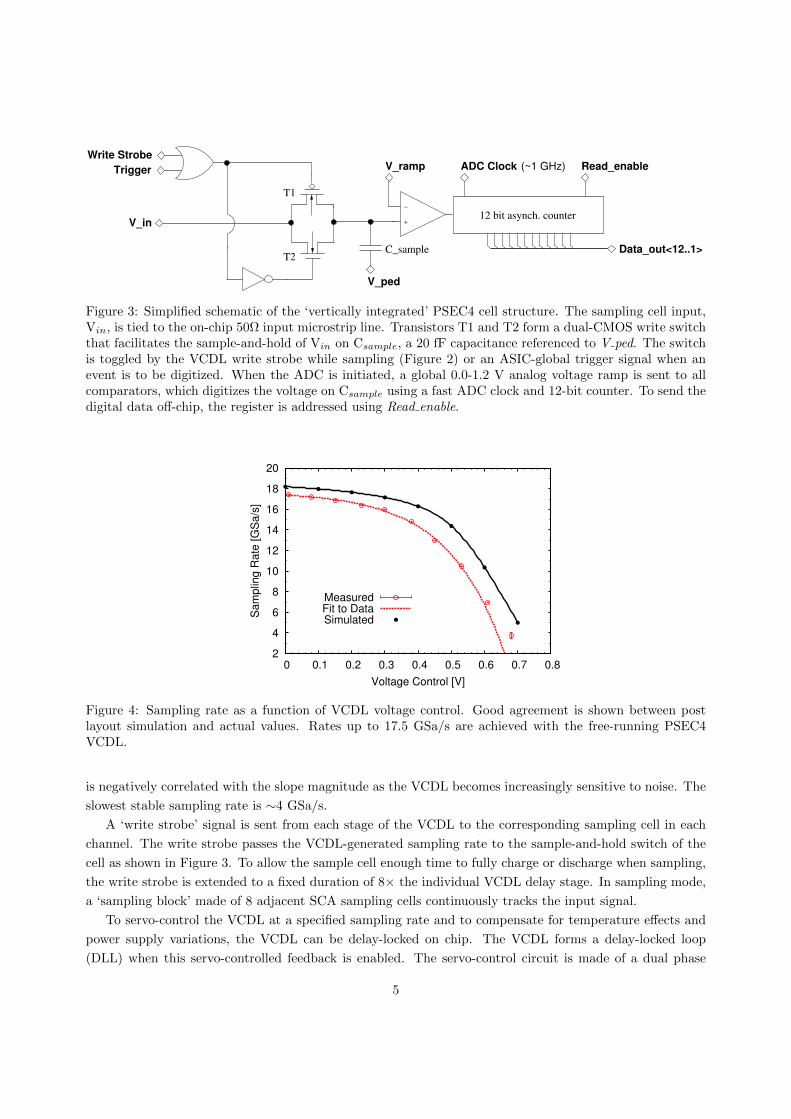
is made from a switched capacitor sampling cell and an integrated ADC circuit as shown in Figure 3.
To operate the chip, a field-programmable gate array (FPGA) is used to provide timing control, clock
generation, readout addressing, data management, and general configurations to the ASIC. Several analog
3
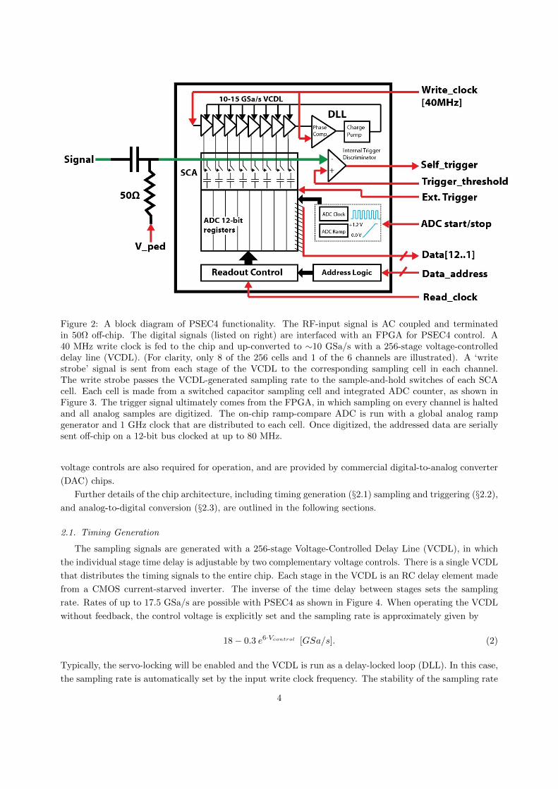
Figure 2: A block diagram of PSEC4 functionality. The RF-input signal is AC coupled and terminatedin 50Ω off-chip. The digital signals (listed on right) are interfaced with an FPGA for PSEC4 control. A40 MHz write clock is fed to the chip and up-converted to ∼10 GSa/s with a 256-stage voltage-controlleddelay line (VCDL). (For clarity, only 8 of the 256 cells and 1 of the 6 channels are illustrated). A ‘writestrobe’ signal is sent from each stage of the VCDL to the corresponding sampling cell in each channel.The write strobe passes the VCDL-generated sampling rate to the sample-and-hold switches of each SCAcell. Each cell is made from a switched capacitor sampling cell and integrated ADC counter, as shown inFigure 3. The trigger signal ultimately comes from the FPGA, in which sampling on every channel is haltedand all analog samples are digitized. The on-chip ramp-compare ADC is run with a global analog rampgenerator and 1 GHz clock that are distributed to each cell. Once digitized, the addressed data are seriallysent off-chip on a 12-bit bus clocked at up to 80 MHz.
voltage controls are also required for operation, and are provided by commercial digital-to-analog converter
(DAC) chips.
Further details of the chip architecture, including timing generation (§2.1) sampling and triggering (§2.2),
and analog-to-digital conversion (§2.3), are outlined in the following sections.
2.1. Timing Generation
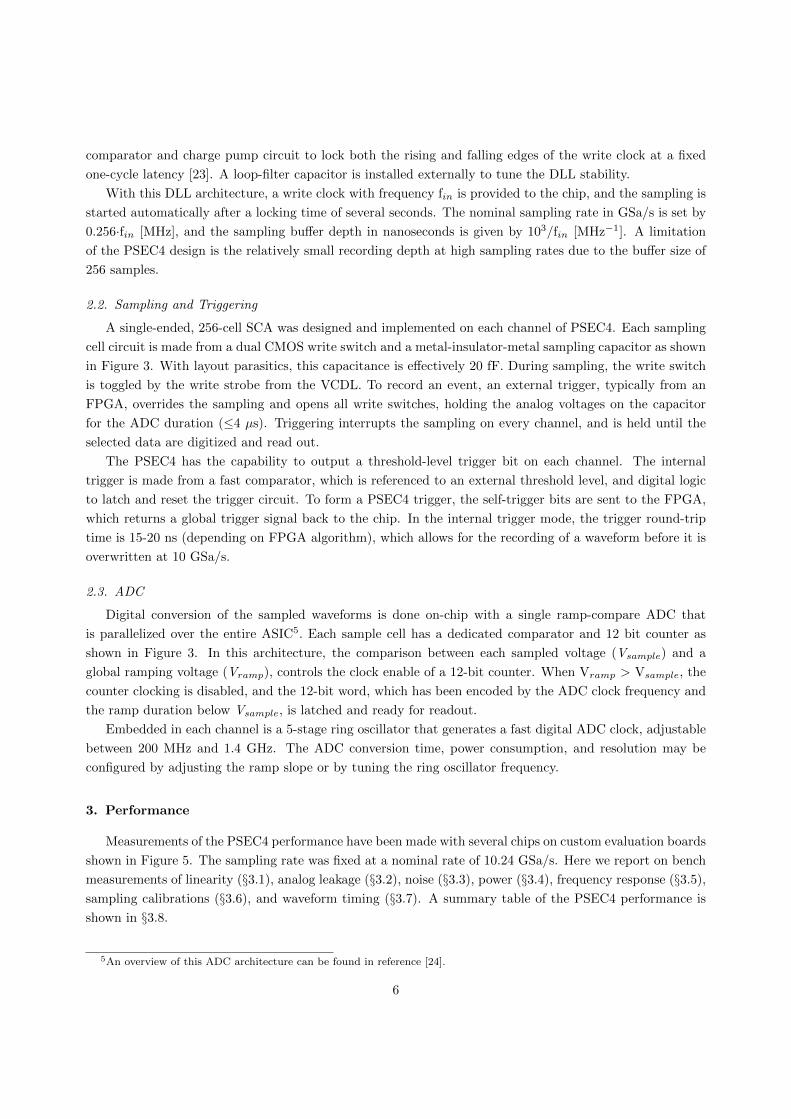
The sampling signals are generated with a 256-stage Voltage-Controlled Delay Line (VCDL), in which
the individual stage time delay is adjustable by two complementary voltage controls. There is a single VCDL
that distributes the timing signals to the entire chip. Each stage in the VCDL is an RC delay element made
from a CMOS current-starved inverter. The inverse of the time delay between stages sets the sampling
rate. Rates of up to 17.5 GSa/s are possible with PSEC4 as shown in Figure 4. When operating the VCDL
without feedback, the control voltage is explicitly set and the sampling rate is approximately given by
18− 0.3 e6·Vcontrol [GSa/s]. (2)
Typically, the servo-locking will be enabled and the VCDL is run as a delay-locked loop (DLL). In this case,
the sampling rate is automatically set by the input write clock frequency. The stability of the sampling rate
4
ADC Clock Read_enableV_ramp
C_sample
T1
T2
(~1 GHz)Write Strobe
Trigger
V_in
Data_out<12..1>
V_ped
12 bit asynch. counter+
−
Figure 3: Simplified schematic of the ‘vertically integrated’ PSEC4 cell structure. The sampling cell input,Vin, is tied to the on-chip 50Ω input microstrip line. Transistors T1 and T2 form a dual-CMOS write switchthat facilitates the sample-and-hold of Vin on Csample, a 20 fF capacitance referenced to V ped. The switchis toggled by the VCDL write strobe while sampling (Figure 2) or an ASIC-global trigger signal when anevent is to be digitized. When the ADC is initiated, a global 0.0-1.2 V analog voltage ramp is sent to allcomparators, which digitizes the voltage on Csample using a fast ADC clock and 12-bit counter. To send thedigital data off-chip, the register is addressed using Read enable.
2
4
6
8
10
12
14
16
18
20
0 0.1 0.2 0.3 0.4 0.5 0.6 0.7 0.8
Sa
mp
ling
Ra
te [
GS
a/s
]
Voltage Control [V]
MeasuredFit to DataSimulated
Figure 4: Sampling rate as a function of VCDL voltage control. Good agreement is shown between postlayout simulation and actual values. Rates up to 17.5 GSa/s are achieved with the free-running PSEC4VCDL.
is negatively correlated with the slope magnitude as the VCDL becomes increasingly sensitive to noise. The
slowest stable sampling rate is ∼4 GSa/s.
A ‘write strobe’ signal is sent from each stage of the VCDL to the corresponding sampling cell in each
channel. The write strobe passes the VCDL-generated sampling rate to the sample-and-hold switch of the
cell as shown in Figure 3. To allow the sample cell enough time to fully charge or discharge when sampling,
the write strobe is extended to a fixed duration of 8× the individual VCDL delay stage. In sampling mode,
a ‘sampling block’ made of 8 adjacent SCA sampling cells continuously tracks the input signal.
To servo-control the VCDL at a specified sampling rate and to compensate for temperature effects and
power supply variations, the VCDL can be delay-locked on chip. The VCDL forms a delay-locked loop
(DLL) when this servo-controlled feedback is enabled. The servo-control circuit is made of a dual phase
5
comparator and charge pump circuit to lock both the rising and falling edges of the write clock at a fixed
one-cycle latency [23]. A loop-filter capacitor is installed externally to tune the DLL stability.
With this DLL architecture, a write clock with frequency fin is provided to the chip, and the sampling is
started automatically after a locking time of several seconds. The nominal sampling rate in GSa/s is set by
0.256·fin [MHz], and the sampling buffer depth in nanoseconds is given by 103/fin [MHz−1]. A limitation
of the PSEC4 design is the relatively small recording depth at high sampling rates due to the buffer size of
256 samples.
2.2. Sampling and Triggering
A single-ended, 256-cell SCA was designed and implemented on each channel of PSEC4. Each sampling
cell circuit is made from a dual CMOS write switch and a metal-insulator-metal sampling capacitor as shown
in Figure 3. With layout parasitics, this capacitance is effectively 20 fF. During sampling, the write switch
is toggled by the write strobe from the VCDL. To record an event, an external trigger, typically from an
FPGA, overrides the sampling and opens all write switches, holding the analog voltages on the capacitor
for the ADC duration (≤4 µs). Triggering interrupts the sampling on every channel, and is held until the
selected data are digitized and read out.
The PSEC4 has the capability to output a threshold-level trigger bit on each channel. The internal
trigger is made from a fast comparator, which is referenced to an external threshold level, and digital logic
to latch and reset the trigger circuit. To form a PSEC4 trigger, the self-trigger bits are sent to the FPGA,
which returns a global trigger signal back to the chip. In the internal trigger mode, the trigger round-trip
time is 15-20 ns (depending on FPGA algorithm), which allows for the recording of a waveform before it is
overwritten at 10 GSa/s.
2.3. ADC
Digital conversion of the sampled waveforms is done on-chip with a single ramp-compare ADC that
is parallelized over the entire ASIC5. Each sample cell has a dedicated comparator and 12 bit counter as
shown in Figure 3. In this architecture, the comparison between each sampled voltage (Vsample) and a
global ramping voltage (Vramp), controls the clock enable of a 12-bit counter. When Vramp > Vsample, the
counter clocking is disabled, and the 12-bit word, which has been encoded by the ADC clock frequency and
the ramp duration below Vsample, is latched and ready for readout.
Embedded in each channel is a 5-stage ring oscillator that generates a fast digital ADC clock, adjustable
between 200 MHz and 1.4 GHz. The ADC conversion time, power consumption, and resolution may be
configured by adjusting the ramp slope or by tuning the ring oscillator frequency.
3. Performance
Measurements of the PSEC4 performance have been made with several chips on custom evaluation boards
shown in Figure 5. The sampling rate was fixed at a nominal rate of 10.24 GSa/s. Here we report on bench
measurements of linearity (§3.1), analog leakage (§3.2), noise (§3.3), power (§3.4), frequency response (§3.5),
sampling calibrations (§3.6), and waveform timing (§3.7). A summary table of the PSEC4 performance is
shown in §3.8.
5An overview of this ADC architecture can be found in reference [24].
6
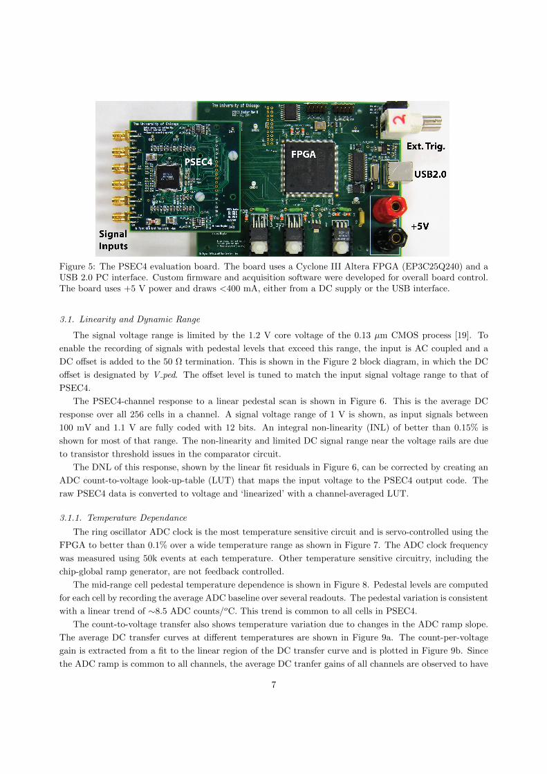
Figure 5: The PSEC4 evaluation board. The board uses a Cyclone III Altera FPGA (EP3C25Q240) and aUSB 2.0 PC interface. Custom firmware and acquisition software were developed for overall board control.The board uses +5 V power and draws <400 mA, either from a DC supply or the USB interface.
3.1. Linearity and Dynamic Range
The signal voltage range is limited by the 1.2 V core voltage of the 0.13 µm CMOS process [19]. To
enable the recording of signals with pedestal levels that exceed this range, the input is AC coupled and a
DC offset is added to the 50 Ω termination. This is shown in the Figure 2 block diagram, in which the DC
offset is designated by V ped. The offset level is tuned to match the input signal voltage range to that of
PSEC4.
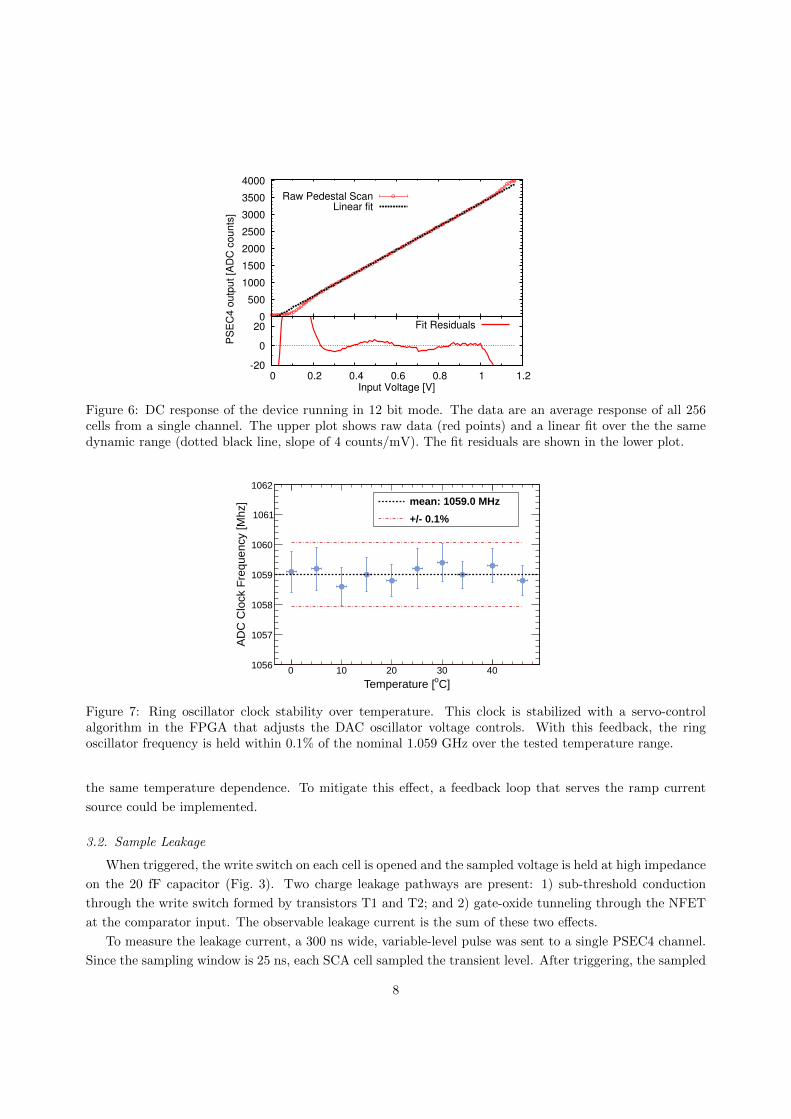
The PSEC4-channel response to a linear pedestal scan is shown in Figure 6. This is the average DC
response over all 256 cells in a channel. A signal voltage range of 1 V is shown, as input signals between
100 mV and 1.1 V are fully coded with 12 bits. An integral non-linearity (INL) of better than 0.15% is
shown for most of that range. The non-linearity and limited DC signal range near the voltage rails are due
to transistor threshold issues in the comparator circuit.
The DNL of this response, shown by the linear fit residuals in Figure 6, can be corrected by creating an
ADC count-to-voltage look-up-table (LUT) that maps the input voltage to the PSEC4 output code. The
raw PSEC4 data is converted to voltage and ‘linearized’ with a channel-averaged LUT.
3.1.1. Temperature Dependance
The ring oscillator ADC clock is the most temperature sensitive circuit and is servo-controlled using the
FPGA to better than 0.1% over a wide temperature range as shown in Figure 7. The ADC clock frequency
was measured using 50k events at each temperature. Other temperature sensitive circuitry, including the
chip-global ramp generator, are not feedback controlled.
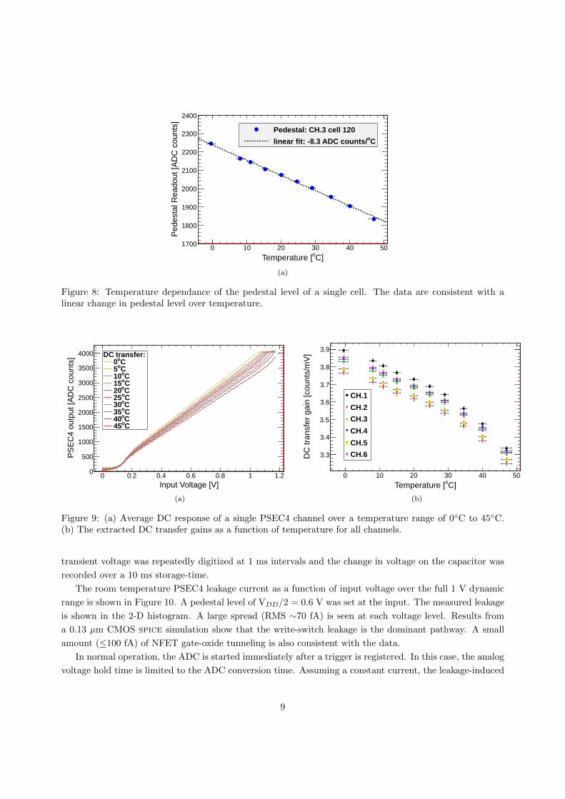
The mid-range cell pedestal temperature dependence is shown in Figure 8. Pedestal levels are computed
for each cell by recording the average ADC baseline over several readouts. The pedestal variation is consistent
with a linear trend of ∼8.5 ADC counts/oC. This trend is common to all cells in PSEC4.
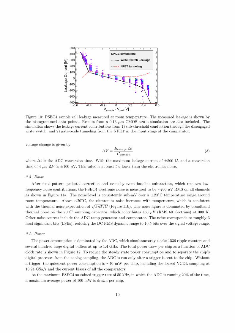
The count-to-voltage transfer also shows temperature variation due to changes in the ADC ramp slope.
The average DC transfer curves at different temperatures are shown in Figure 9a. The count-per-voltage
gain is extracted from a fit to the linear region of the DC transfer curve and is plotted in Figure 9b. Since
the ADC ramp is common to all channels, the average DC tranfer gains of all channels are observed to have
7
-20
0
20
0 0.2 0.4 0.6 0.8 1 1.2Input Voltage [V]
Fit Residuals 0
500
1000
1500
2000
2500
3000
3500
4000
PS
EC
4 o
utp
ut [A
DC
counts
]
Raw Pedestal ScanLinear fit
Figure 6: DC response of the device running in 12 bit mode. The data are an average response of all 256cells from a single channel. The upper plot shows raw data (red points) and a linear fit over the the samedynamic range (dotted black line, slope of 4 counts/mV). The fit residuals are shown in the lower plot.
C]oTemperature [0 10 20 30 40
AD
C C
lock
Fre
quen
cy [M
hz]
1056
1057
1058
1059
1060
1061
1062
mean: 1059.0 MHz
+/- 0.1%
Figure 7: Ring oscillator clock stability over temperature. This clock is stabilized with a servo-controlalgorithm in the FPGA that adjusts the DAC oscillator voltage controls. With this feedback, the ringoscillator frequency is held within 0.1% of the nominal 1.059 GHz over the tested temperature range.
the same temperature dependence. To mitigate this effect, a feedback loop that serves the ramp current
source could be implemented.
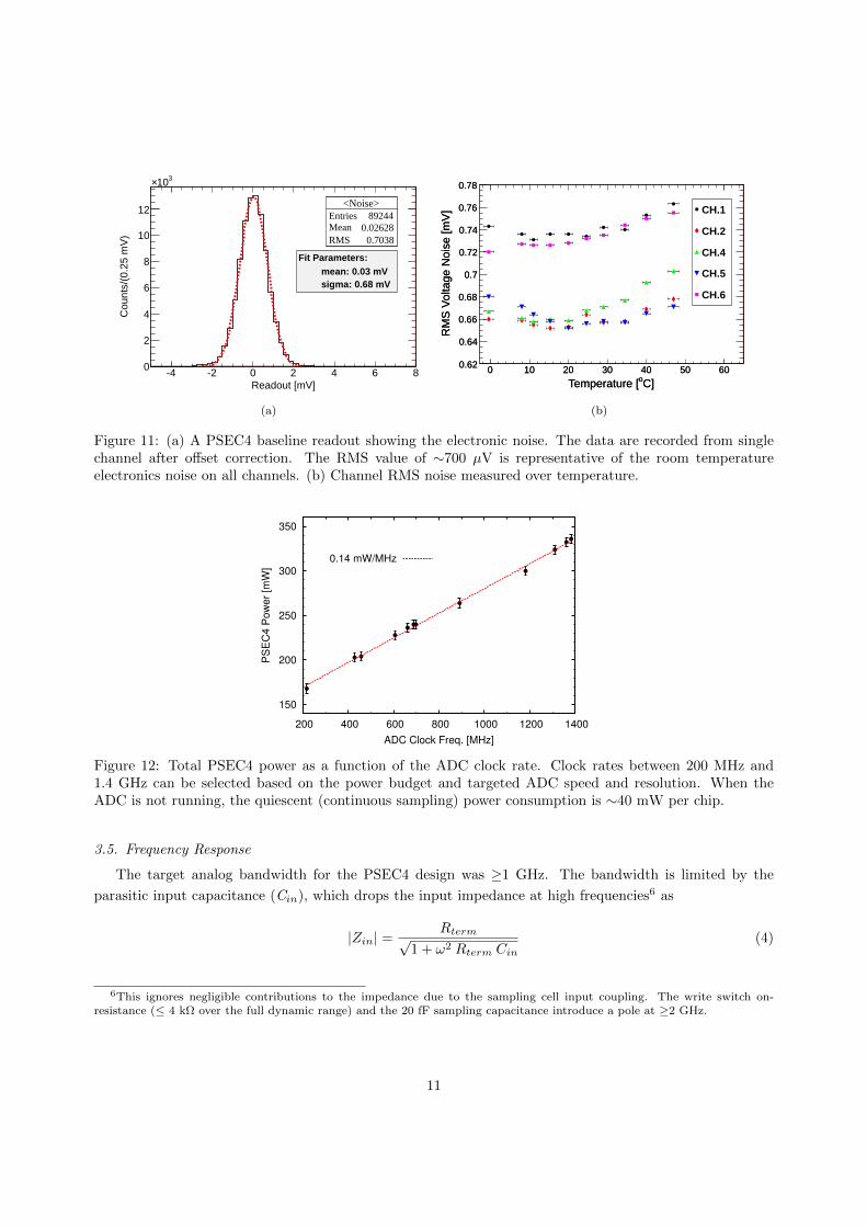
3.2. Sample Leakage
When triggered, the write switch on each cell is opened and the sampled voltage is held at high impedance
on the 20 fF capacitor (Fig. 3). Two charge leakage pathways are present: 1) sub-threshold conduction
through the write switch formed by transistors T1 and T2; and 2) gate-oxide tunneling through the NFET
at the comparator input. The observable leakage current is the sum of these two effects.
To measure the leakage current, a 300 ns wide, variable-level pulse was sent to a single PSEC4 channel.
Since the sampling window is 25 ns, each SCA cell sampled the transient level. After triggering, the sampled
8
C]oTemperature [0 10 20 30 40 50
Ped
esta
l Rea
dout
[AD
C c
ount
s]
1700
1800
1900
2000
2100
2200
2300
2400
Pedestal: CH.3 cell 120
Colinear fit: -8.3 ADC counts/
(a)
Figure 8: Temperature dependance of the pedestal level of a single cell. The data are consistent with alinear change in pedestal level over temperature.
Input Voltage [V]0 0.2 0.4 0.6 0.8 1 1.2
PS
EC
4 ou
tput
[AD
C c
ount
s]
0
500
1000
1500
2000
2500
3000
3500
4000 DC transfer:Co0Co5Co10Co15Co20Co25Co30Co35Co40Co45
(a)
C]oTemperature [0 10 20 30 40 50
DC
tran
sfer
gai
n [c
ount
s/m
V]
3.3
3.4
3.5
3.6
3.7
3.8
3.9
CH.1
CH.2
CH.3
CH.4
CH.5
CH.6
(b)
Figure 9: (a) Average DC response of a single PSEC4 channel over a temperature range of 0C to 45C.(b) The extracted DC transfer gains as a function of temperature for all channels.
transient voltage was repeatedly digitized at 1 ms intervals and the change in voltage on the capacitor was
recorded over a 10 ms storage-time.
The room temperature PSEC4 leakage current as a function of input voltage over the full 1 V dynamic
range is shown in Figure 10. A pedestal level of VDD/2 = 0.6 V was set at the input. The measured leakage
is shown in the 2-D histogram. A large spread (RMS ∼70 fA) is seen at each voltage level. Results from
a 0.13 µm CMOS spice simulation show that the write-switch leakage is the dominant pathway. A small
amount (≤100 fA) of NFET gate-oxide tunneling is also consistent with the data.
In normal operation, the ADC is started immediately after a trigger is registered. In this case, the analog
voltage hold time is limited to the ADC conversion time. Assuming a constant current, the leakage-induced
9
[V]ped - VsampleV-0.6 -0.4 -0.2 0 0.2 0.4 0.6
Leak
age
Cur
rent
[fA
]
-400
-300
-200
-100
0
100
200
300
400
500
SPICE simulation:
Write Switch Leakage
NFET tunneling
Figure 10: PSEC4 sample cell leakage measured at room temperature. The measured leakage is shown bythe histogrammed data points. Results from a 0.13 µm CMOS spice simulation are also included. Thesimulation shows the leakage current contributions from 1) sub-threshold conduction through the disengagedwrite switch; and 2) gate-oxide tunneling from the NFET in the input stage of the comparator.
voltage change is given by
∆V =Ileakage ∆t
Csample(3)
where ∆t is the ADC conversion time. With the maximum leakage current of ±500 fA and a conversion
time of 4 µs, ∆V is ±100 µV. This value is at least 5× lower than the electronics noise.
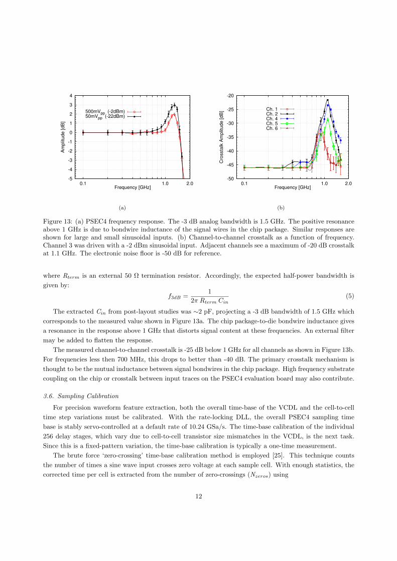
3.3. Noise
After fixed-pattern pedestal correction and event-by-event baseline subtraction, which removes low-
frequency noise contributions, the PSEC4 electronic noise is measured to be ∼700 µV RMS on all channels
as shown in Figure 11a. The noise level is consistently sub-mV over a ±20C temperature range around
room temperature. Above ∼20C, the electronics noise increases with temperature, which is consistent
with the thermal noise expectation of√kBT/C (Figure 11b). The noise figure is dominated by broadband
thermal noise on the 20 fF sampling capacitor, which contributes 450 µV (RMS 60 electrons) at 300 K.
Other noise sources include the ADC ramp generator and comparator. The noise corresponds to roughly 3
least significant bits (LSBs), reducing the DC RMS dynamic range to 10.5 bits over the signal voltage range.
3.4. Power
The power consumption is dominated by the ADC, which simultaneously clocks 1536 ripple counters and
several hundred large digital buffers at up to 1.4 GHz. The total power draw per chip as a function of ADC
clock rate is shown in Figure 12. To reduce the steady state power consumption and to separate the chip’s
digital processes from the analog sampling, the ADC is run only after a trigger is sent to the chip. Without
a trigger, the quiescent power consumption is ∼40 mW per chip, including the locked VCDL sampling at
10.24 GSa/s and the current biases of all the comparators.
At the maximum PSEC4 sustained trigger rate of 50 kHz, in which the ADC is running 20% of the time,
a maximum average power of 100 mW is drawn per chip.
10
<Noise>Entries 89244Mean 0.02628RMS 0.7038
Readout [mV]-4 -2 0 2 4 6 8
Cou
nts/
(0.2
5 m
V)
0
2
4
6
8
10
12
310×
<Noise>Entries 89244Mean 0.02628RMS 0.7038
Fit Parameters:mean: 0.03 mVsigma: 0.68 mV
(a)
C]oTemperature [0 10 20 30 40 50 60
RM
S V
olta
ge N
oise
[mV
]
0.62
0.64
0.66
0.68
0.7
0.72
0.74
0.76
0.78
CH.1
CH.2
CH.4
CH.5
CH.6
C]oTemperature [0 10 20 30 40 50 60
RM
S V
olta
ge N
oise
[mV
]
0.62
0.64
0.66
0.68
0.7
0.72
0.74
0.76
0.78
CH.1
CH.2
CH.4
CH.5
CH.6
(b)
Figure 11: (a) A PSEC4 baseline readout showing the electronic noise. The data are recorded from singlechannel after offset correction. The RMS value of ∼700 µV is representative of the room temperatureelectronics noise on all channels. (b) Channel RMS noise measured over temperature.
150
200
250
300
350
200 400 600 800 1000 1200 1400
PS
EC
4 P
ow
er
[mW
]
ADC Clock Freq. [MHz]
0.14 mW/MHz
Figure 12: Total PSEC4 power as a function of the ADC clock rate. Clock rates between 200 MHz and1.4 GHz can be selected based on the power budget and targeted ADC speed and resolution. When theADC is not running, the quiescent (continuous sampling) power consumption is ∼40 mW per chip.
3.5. Frequency Response
The target analog bandwidth for the PSEC4 design was ≥1 GHz. The bandwidth is limited by the
parasitic input capacitance (Cin), which drops the input impedance at high frequencies6 as
|Zin| =Rterm√
1 + ω2 Rterm Cin
(4)
6This ignores negligible contributions to the impedance due to the sampling cell input coupling. The write switch on-resistance (≤ 4 kΩ over the full dynamic range) and the 20 fF sampling capacitance introduce a pole at ≥2 GHz.
11
-5
-4
-3
-2
-1
0
1
2
3
4
0.1 1.0 2.0
Am
plit
ud
e [
dB
]
Frequency [GHz]
500mVpp (-2dBm)50mVpp (-22dBm)
(a)
-50
-45
-40
-35
-30
-25
-20
0.1 1.0 2.0
Cro
ssta
lk A
mp
litu
de
[d
B]
Frequency [GHz]
Ch. 1Ch. 2Ch. 4Ch. 5Ch. 6
(b)
Figure 13: (a) PSEC4 frequency response. The -3 dB analog bandwidth is 1.5 GHz. The positive resonanceabove 1 GHz is due to bondwire inductance of the signal wires in the chip package. Similar responses areshown for large and small sinusoidal inputs. (b) Channel-to-channel crosstalk as a function of frequency.Channel 3 was driven with a -2 dBm sinusoidal input. Adjacent channels see a maximum of -20 dB crosstalkat 1.1 GHz. The electronic noise floor is -50 dB for reference.
where Rterm is an external 50 Ω termination resistor. Accordingly, the expected half-power bandwidth is
given by:
f3dB =1
2π Rterm Cin(5)
The extracted Cin from post-layout studies was ∼2 pF, projecting a -3 dB bandwidth of 1.5 GHz which
corresponds to the measured value shown in Figure 13a. The chip package-to-die bondwire inductance gives
a resonance in the response above 1 GHz that distorts signal content at these frequencies. An external filter
may be added to flatten the response.
The measured channel-to-channel crosstalk is -25 dB below 1 GHz for all channels as shown in Figure 13b.
For frequencies less then 700 MHz, this drops to better than -40 dB. The primary crosstalk mechanism is
thought to be the mutual inductance between signal bondwires in the chip package. High frequency substrate
coupling on the chip or crosstalk between input traces on the PSEC4 evaluation board may also contribute.
3.6. Sampling Calibration
For precision waveform feature extraction, both the overall time-base of the VCDL and the cell-to-cell
time step variations must be calibrated. With the rate-locking DLL, the overall PSEC4 sampling time
base is stably servo-controlled at a default rate of 10.24 GSa/s. The time-base calibration of the individual
256 delay stages, which vary due to cell-to-cell transistor size mismatches in the VCDL, is the next task.
Since this is a fixed-pattern variation, the time-base calibration is typically a one-time measurement.
The brute force ‘zero-crossing’ time-base calibration method is employed [25]. This technique counts
the number of times a sine wave input crosses zero voltage at each sample cell. With enough statistics, the
corrected time per cell is extracted from the number of zero-crossings (Nzeros) using
12
Time calibrationEntries 256Mean 0.09601RMS 0.01202
Time-base calibration constants [ns]0.04 0.06 0.08 0.1 0.12 0.14 0.16 0.18 0.2
Ent
ries/
(6.5
ps)
0
10
20
30
40
50
Time calibrationEntries 256Mean 0.09601RMS 0.01202
Fit Parameters:
mean: 95.9 ps
sigma: 12.1 ps
(a)
PSEC4 sampling cell no.0 50 100 150 200 250
Tim
e [n
s]
-0.05
0
0.05
0.1
0.15
0.2
0.25
0.3
0.35
0.4Time-base:
DNLINL
DLL wrap-around offset
(b)
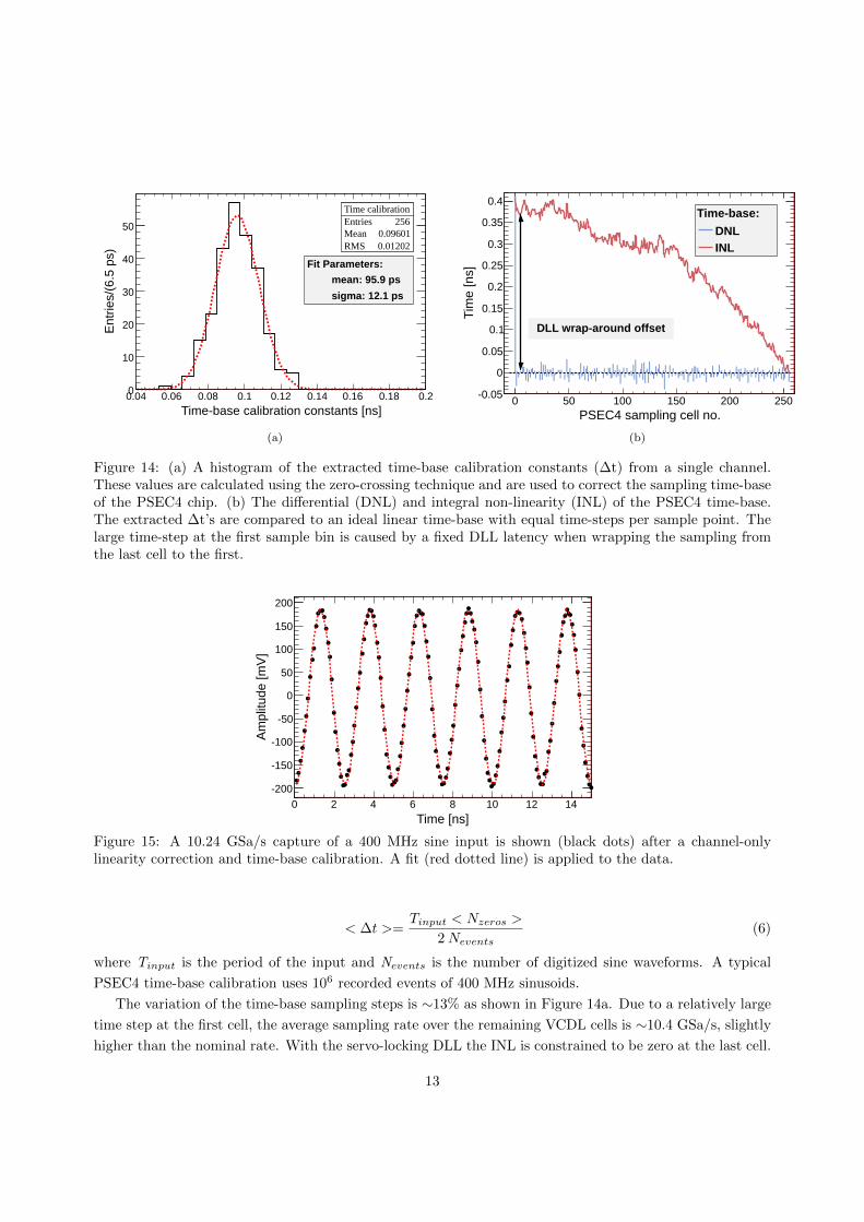
Figure 14: (a) A histogram of the extracted time-base calibration constants (∆t) from a single channel.These values are calculated using the zero-crossing technique and are used to correct the sampling time-baseof the PSEC4 chip. (b) The differential (DNL) and integral non-linearity (INL) of the PSEC4 time-base.The extracted ∆t’s are compared to an ideal linear time-base with equal time-steps per sample point. Thelarge time-step at the first sample bin is caused by a fixed DLL latency when wrapping the sampling fromthe last cell to the first.
Time [ns]0 2 4 6 8 10 12 14
Am
plitu
de [m
V]
-200
-150
-100
-50
0
50
100
150
200
Figure 15: A 10.24 GSa/s capture of a 400 MHz sine input is shown (black dots) after a channel-onlylinearity correction and time-base calibration. A fit (red dotted line) is applied to the data.
< ∆t >=Tinput < Nzeros >
2Nevents(6)
where Tinput is the period of the input and Nevents is the number of digitized sine waveforms. A typical
PSEC4 time-base calibration uses 106 recorded events of 400 MHz sinusoids.
The variation of the time-base sampling steps is ∼13% as shown in Figure 14a. Due to a relatively large
time step at the first cell, the average sampling rate over the remaining VCDL cells is ∼10.4 GSa/s, slightly
higher than the nominal rate. With the servo-locking DLL the INL is constrained to be zero at the last cell.
13
C]oTemperature [0 10 20 30 40 50
Mea
n S
ampl
ing
Tim
e-st
ep [p
s]
95
95.5
96
96.5
97
97.5
98
Sampling Rate: 10.37 GSa/s
C]oTemperature [0 10 20 30 40 50
Mea
n S
ampl
ing
Tim
e-st
ep [p
s]
95
95.5
96
96.5
97
97.5
98
Sampling Rate: 10.37 GSa/s
C]oTemperature [0 10 20 30 40 50
Mea
n S
ampl
ing
Tim
e-st
ep [p
s]
95
95.5
96
96.5
97
97.5
98
Sampling Rate: 10.37 GSa/s
C]oTemperature [0 10 20 30 40 50
Mea
n S
ampl
ing
Tim
e-st
ep [p
s]
95
95.5
96
96.5
97
97.5
98
Sampling Rate: 10.37 GSa/s
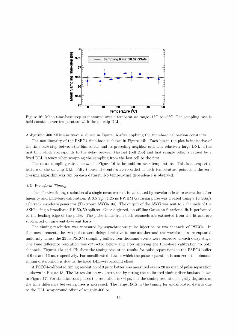
Figure 16: Mean time-base step as measured over a temperature range -1C to 46C. The sampling rate isheld constant over temperature with the on-chip DLL.
A digitized 400 MHz sine wave is shown in Figure 15 after applying the time-base calibration constants.
The non-linearity of the PSEC4 time-base is shown in Figure 14b. Each bin in the plot is indicative of
the time-base step between the binned cell and its preceding neighbor cell. The relatively large DNL in the
first bin, which corresponds to the delay between the last (cell 256) and first sample cells, is caused by a
fixed DLL latency when wrapping the sampling from the last cell to the first.
The mean sampling rate is shown in Figure 16 to be uniform over temperature. This is an expected
feature of the on-chip DLL. Fifty-thousand events were recorded at each temperature point and the zero
crossing algorithm was run on each dataset. No temperature dependence is observed.
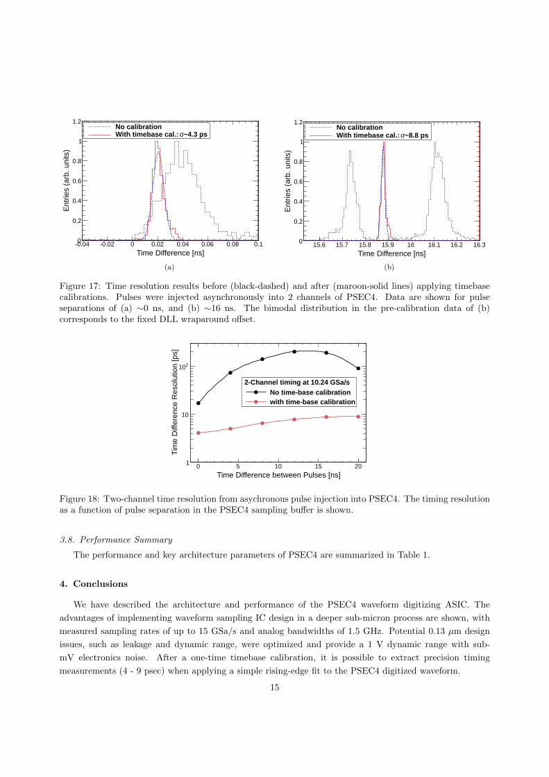
3.7. Waveform Timing
The effective timing resolution of a single measurement is calculated by waveform feature extraction after
linearity and time-base calibration. A 0.5 Vpp, 1.25 ns FWHM Gaussian pulse was created using a 10 GSa/s
arbitrary waveform generator (Tektronix AWG5104). The output of the AWG was sent to 2 channels of the
ASIC using a broadband-RF 50/50 splitter. Once digitized, an off-line Gaussian functional fit is performed
to the leading edge of the pulse. The pulse times from both channels are extracted from the fit and are
subtracted on an event-by-event basis.
The timing resolution was measured by asynchronous pulse injection to two channels of PSEC4. In
this measurement, the two pulses were delayed relative to one-another and the waveforms were captured
uniformly across the 25 ns PSEC4 sampling buffer. Ten-thousand events were recorded at each delay stage.
The time difference resolution was extracted before and after applying the time-base calibration to both
channels. Figures 17a and 17b show the timing resolution results for pulse separations in the PSEC4 buffer
of 0 ns and 16 ns, respectively. For uncalibrated data in which the pulse separation is non-zero, the bimodal
timing distribution is due to the fixed DLL-wraparound offset.
A PSEC4-calibrated timing resolution of 9 ps or better was measured over a 20 ns span of pulse separation
as shown in Figure 18. The 1σ resolution was extracted by fitting the calibrated timing distributions shown
in Figure 17. For simultaneous pulses the resolution is ∼4 ps, but the timing resolution slightly degrades as
the time difference between pulses is increased. The large RMS in the timing for uncalibrated data is due
to the DLL wraparound offset of roughly 400 ps.
14
Time Difference [ns]-0.04 -0.02 0 0.02 0.04 0.06 0.08 0.1
Ent
ries
(arb
. uni
ts)
0
0.2
0.4
0.6
0.8
1
1.2No calibration
~4.3 ps σWith timebase cal.:
(a)
Time Difference [ns]15.6 15.7 15.8 15.9 16 16.1 16.2 16.3
Ent
ries
(arb
. uni
ts)
0
0.2
0.4
0.6
0.8
1
1.2No calibration
~8.8 psσWith timebase cal.:
(b)
Figure 17: Time resolution results before (black-dashed) and after (maroon-solid lines) applying timebasecalibrations. Pulses were injected asynchronously into 2 channels of PSEC4. Data are shown for pulseseparations of (a) ∼0 ns, and (b) ∼16 ns. The bimodal distribution in the pre-calibration data of (b)corresponds to the fixed DLL wraparound offset.
Time Difference between Pulses [ns]0 5 10 15 20
Tim
e D
iffer
ence
Res
olut
ion
[ps]
1
10
210
2-Channel timing at 10.24 GSa/sNo time-base calibrationwith time-base calibration
Figure 18: Two-channel time resolution from asychronous pulse injection into PSEC4. The timing resolutionas a function of pulse separation in the PSEC4 sampling buffer is shown.
3.8. Performance Summary
The performance and key architecture parameters of PSEC4 are summarized in Table 1.
4. Conclusions
We have described the architecture and performance of the PSEC4 waveform digitizing ASIC. The
advantages of implementing waveform sampling IC design in a deeper sub-micron process are shown, with
measured sampling rates of up to 15 GSa/s and analog bandwidths of 1.5 GHz. Potential 0.13 µm design
issues, such as leakage and dynamic range, were optimized and provide a 1 V dynamic range with sub-
mV electronics noise. After a one-time timebase calibration, it is possible to extract precision timing
measurements (4 - 9 psec) when applying a simple rising-edge fit to the PSEC4 digitized waveform.
15
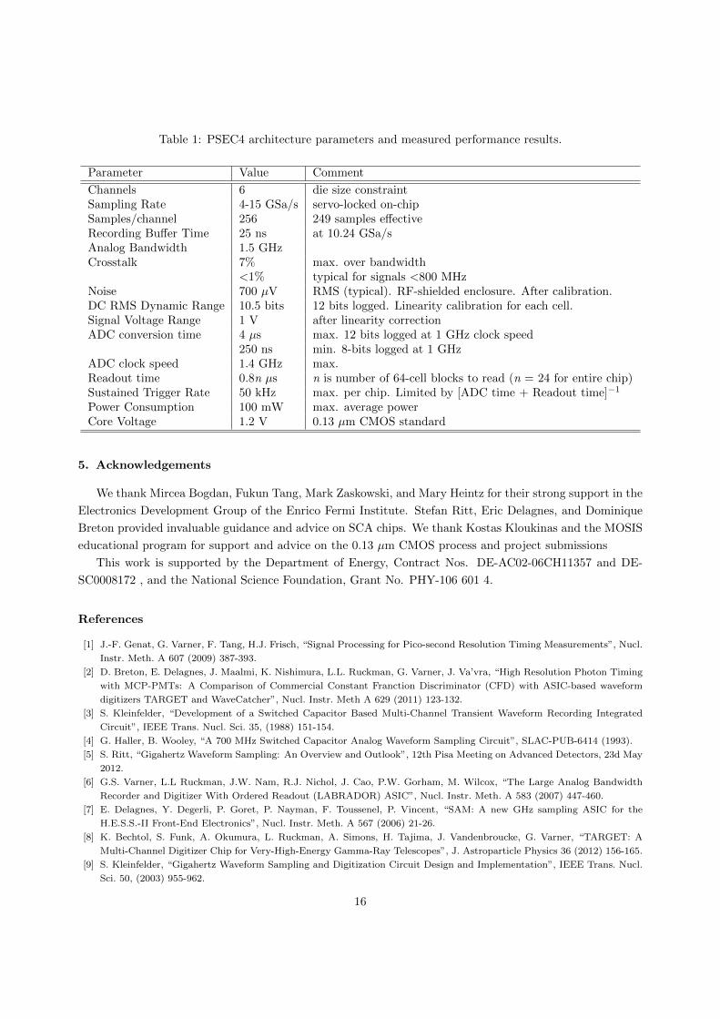
Table 1: PSEC4 architecture parameters and measured performance results.
Parameter Value Comment
Channels 6 die size constraintSampling Rate 4-15 GSa/s servo-locked on-chipSamples/channel 256 249 samples effectiveRecording Buffer Time 25 ns at 10.24 GSa/sAnalog Bandwidth 1.5 GHzCrosstalk 7% max. over bandwidth
<1% typical for signals <800 MHzNoise 700 µV RMS (typical). RF-shielded enclosure. After calibration.DC RMS Dynamic Range 10.5 bits 12 bits logged. Linearity calibration for each cell.Signal Voltage Range 1 V after linearity correctionADC conversion time 4 µs max. 12 bits logged at 1 GHz clock speed
250 ns min. 8-bits logged at 1 GHzADC clock speed 1.4 GHz max.Readout time 0.8n µs n is number of 64-cell blocks to read (n = 24 for entire chip)Sustained Trigger Rate 50 kHz max. per chip. Limited by [ADC time + Readout time]−1
Power Consumption 100 mW max. average powerCore Voltage 1.2 V 0.13 µm CMOS standard
5. Acknowledgements
We thank Mircea Bogdan, Fukun Tang, Mark Zaskowski, and Mary Heintz for their strong support in the
Electronics Development Group of the Enrico Fermi Institute. Stefan Ritt, Eric Delagnes, and Dominique
Breton provided invaluable guidance and advice on SCA chips. We thank Kostas Kloukinas and the MOSIS
educational program for support and advice on the 0.13 µm CMOS process and project submissions
This work is supported by the Department of Energy, Contract Nos. DE-AC02-06CH11357 and DE-
SC0008172 , and the National Science Foundation, Grant No. PHY-106 601 4.
References
[1] J.-F. Genat, G. Varner, F. Tang, H.J. Frisch, “Signal Processing for Pico-second Resolution Timing Measurements”, Nucl.
Instr. Meth. A 607 (2009) 387-393.
[2] D. Breton, E. Delagnes, J. Maalmi, K. Nishimura, L.L. Ruckman, G. Varner, J. Va’vra, “High Resolution Photon Timing
with MCP-PMTs: A Comparison of Commercial Constant Franction Discriminator (CFD) with ASIC-based waveform
digitizers TARGET and WaveCatcher”, Nucl. Instr. Meth A 629 (2011) 123-132.
[3] S. Kleinfelder, “Development of a Switched Capacitor Based Multi-Channel Transient Waveform Recording Integrated
Circuit”, IEEE Trans. Nucl. Sci. 35, (1988) 151-154.
[4] G. Haller, B. Wooley, “A 700 MHz Switched Capacitor Analog Waveform Sampling Circuit”, SLAC-PUB-6414 (1993).
[5] S. Ritt, “Gigahertz Waveform Sampling: An Overview and Outlook”, 12th Pisa Meeting on Advanced Detectors, 23d May
2012.
[6] G.S. Varner, L.L Ruckman, J.W. Nam, R.J. Nichol, J. Cao, P.W. Gorham, M. Wilcox, “The Large Analog Bandwidth
Recorder and Digitizer With Ordered Readout (LABRADOR) ASIC”, Nucl. Instr. Meth. A 583 (2007) 447-460.
[7] E. Delagnes, Y. Degerli, P. Goret, P. Nayman, F. Toussenel, P. Vincent, “SAM: A new GHz sampling ASIC for the
H.E.S.S.-II Front-End Electronics”, Nucl. Instr. Meth. A 567 (2006) 21-26.
[8] K. Bechtol, S. Funk, A. Okumura, L. Ruckman, A. Simons, H. Tajima, J. Vandenbroucke, G. Varner, “TARGET: A
Multi-Channel Digitizer Chip for Very-High-Energy Gamma-Ray Telescopes”, J. Astroparticle Physics 36 (2012) 156-165.
[9] S. Kleinfelder, “Gigahertz Waveform Sampling and Digitization Circuit Design and Implementation”, IEEE Trans. Nucl.
Sci. 50, (2003) 955-962.
16
[10] G.S. Varner, P. Gorham, J. Cao, “Monolithic Multi-Channel GSa/s Transient Waveform Recorder for Measuring Radio
Emissions from High Energy Particle Cascades”, Proc. SPIE Int. Soc. Opt. Eng 4858 (2003) 31.
[11] C. Broennimann, R. Horisberger, R. Schnyder, “The Domino Sampling Chip: A 1.2 GHz Waveform Sampling CMOS
Chip”, Nucl. Instr. Meth. A 420 (1999) 264-269.
[12] S. Ritt, “The DRS Chip: Cheap Waveform Digitization in the GHz Range”, Nucl. Instr. Meth. A 518 (2004) 470-471.
[13] J. Milnes, J. Howorth, “Picosecond Time Response Characteristics of Micro-channel Plate PMT Detectors”, SPIE USE,
V. 8 5580 (2004) 89-100.
[14] B. Adams, A. Elagin, H. Frisch, R. Obaid, E. Oberla, A. Vostrikov, R. Wagner, M. Wetstein, “Measurements of the Gain,
Time Resolution, and Spatial Resolution of a 20x20 cm2 MCP-based Picosecond Photo-Detector”, Nucl. Instr. Meth. A
(2013), http://dx.doi.org/10.1016/j.nima.2013.07.091.
[15] P. Eraerds, M. Legre, A. Rochas, H. Zbinden, N. Gisin, “SiPM for fast Photon-Counting and Multiphoton Detection”,
Optics Express, Vol. 15 (2007) 14539-14549.
[16] S. Ritt, “The Role of Analog Bandwidth and S/N in Timing”, talk at The Factors that Limit Timing Resolution in
Photodetectors, <http://psec.uchicago.edu/workshops/fast timing conf 2011/>, University of Chicago, Apr 2011.
[17] R.H. Dennard, F. H. Gaennsslen, H. N. Yu, V.L Rideout, E. Bassous, A.R. LeBlanc, “Design of Ion-Implemented MOS-
FETs with Very Small Physical Dimensions,” IEEE J. Solid-State Circuits SC-9 (1974) 256-268.
[18] Y. Taur et. al., “CMOS Scaling into the Nanometer Regime”, Proc. IEEE. Vol. 85, No. 4, (1997) 486-504.
[19] IBM Corporation, “CMRF8SF Model Reference Guide”, V.1.4.0.10 (2008).
[20] The MOSIS Service. Wafer Electrical Test Data and SPICE Model Parameters. Run: V18B. Available on-line (accessed
4 Feb. 2013): <http:://www.mosis.com/pages/Technical/ Testdata/ibm-013-prm>
[21] E. Oberla, H. Grabas, M. Bogdan, H. Frisch, J.-F. Genat, K. Nishimura, G. Varner, A. Wong, “A 4-Channel Waveform
Sampling ASIC in 0.13 µm CMOS for Front-End Readout of Large-Area Micro-Channel Plate Detectors”, Physics Procedia
37 (2012) 1690-1698.
[22] M. Cooney, M. Andrew, K. Nishimura, L. Ruckman, G. Varner, H. Grabas, E. Oberla, J.-F. Genat, “Multipurpose
Test Structures and Process Characterization using 0.13 µm CMOS: The CHAMP ASIC”, Physics Procedia 37 (2012)
1699-1706.
[23] H. Chang et al., “A Wide-Range Delay-Locked Loop With a Fixed Latency of One Clock Cycle”, IEEE J. Solid-State
Circuits 37 (2002) 1021-1027.
[24] O. Milgrome, S. Kleinfelder, M. Levi, “A 12 Bit Analog to Digital Converter for VLSI Applications in Nuclear Science”,
IEEE Trans. Nucl. Sci. 39, (1992) 771-775.
[25] K. Nishimura, A. Romero-Wolf, “A Correlation-Based Timing Calibration & Diagnostic Technique for Fast Digitization
ASICs”, Physics Procedia 37 (2012) 1707-1714.
17