a 15 gsa/s, 1.5 ghz bandwidth waveform digitizing...
TRANSCRIPT
A 15 GSa/s, 1.5 GHz Bandwidth Waveform Digitizing ASIC
Eric Oberlaa, Herve Grabasa,1, Jean-Francois Genata,2, Henry Frischa, Kurtis Nishimurab, Gary Varnerb
aEnrico Fermi Institute, University of Chicago; 5640 S. Ellis Ave., Chicago IL, 60637bUniversity of Hawai’i at Manoa; Watanabe Hall, 2505 Correa Rd., Honolulu HA
Abstract
The PSEC4 custom integrated circuit was designed for the recording of fast waveforms for use in large-area time-of-flight detector systems. The ASIC has been fabricated using the IBM-8RF 0.13 µm CMOSprocess. On each of 6 analog channels, PSEC4 employs a switched capacitor array (SCA) 256 samples deep,a ramp-compare ADC with 10.5 bits of effective resolution, and a serial data readout with the capabilityof region-of-interest windowing to reduce dead time. The sampling rate can be adjusted between 4 and15 Gigasamples/second [GSa/s] on all channels and is servo-controlled on-chip with a low-jitter delay-lockedloop (DLL). The input signals are passively coupled on-chip with a -3dB analog bandwidth of 1.5 GHz.The power consumption in quiescent sampling mode is less than 50 mW/chip; at a sustained trigger andreadout rate of 50 kHz the chip draws 100 mW. After fixed-pattern pedestal subtraction, the uncorrecteddifferential non-linearity is 0.15% over an 800 mV dynamic range. With a linearity correction, a full 1 Vdynamic range is available. The sampling timebase has a fixed-pattern non-linearity of 13%, which canbe calibrated for precision waveform feature extraction and picosecond-level timing resolution. The firstexperimental application to the front-end readout of large-area Micro-Channel Plate (MCP) photodetectorsis presented.
Keywords:Waveform sampling, ASIC, Integrated Circuit, Analog-to-Digital, Switched Capacitor Array
1. Introduction1
We describe the design and performance of2
PSEC4, a ≥10 Gigasample/second [GSa/s] wave-3
form sampling and digitizing Application Spe-4
cific Integrated Circuit (ASIC) fabricated in the5
IBM-8RF 0.13 µm complementary metal-oxide-6
semiconductor (CMOS) technology. This compact7
‘oscilloscope-on-a-chip’ is designed for the recording8
of radio-frequency (RF) transient waveforms with9
signal bandwidths between 100 MHz and 1.5 GHz.10
1Present address, Laboratoire LDEF, CEA/SEDI; CENSaclay-BAT141 F-91191 Gif-sur-Yvette CEDEX, France
2Present address, LPNHE, CNRS/IN2P3, UniversitesPierre et Marie Curie and Denis Diderot, T33 RC, 4 PlaceJussieu 75252 Paris CEDEX 05, France
1.1. Background11
The detection of discrete photons and high-12
energy particles is the basis of a wide range of com-13
mercial and scientific applications. In many of these14
applications, the relative arrival time of an inci-15
dent photon or particle is best measured by extract-16
ing features from the full waveform at the detec-17
tor output [1, 2]. Additional benefits of front-end18
waveform sampling include the detection of pile-19
up events and the ability to filter noise or poorly20
formed pulses.21
For recording ‘snapshots’ of transient waveforms,22
switched capacitor array (SCA) analog memories23
can be used to sample a limited time-window at a24
relatively high rate, but with a latency-cost of a25
Preprint submitted to elsevier February 11, 2013
slower readout speed [3, 4]. These devices are well26
suited for triggered-event applications, as in many27
high energy physics experiments, in which some28
dead-time can be afforded on each channel. With29
modern CMOS integrated circuit design, these SCA30
sampling chips may be compact, low power, and31
relatively low cost per channel [4].32
Over the last decade, sampling rates in SCA33
waveform sampling ASICs have been pushed to sev-34
eral GSa/s with analog bandwidths of several hun-35
dred MHz [5]. As a scalable front-end readout36
option coupled with the advantages of waveform37
sampling, these ASICs have been used in a wide38
range of experiments; such as high-energy physics39
colliders [6], gamma-ray astronomy [7, 8], high-40
energy neutrino detection [9, 10], and rare decay41
searches [11, 12].42
1.2. Motivation43
A natural extension to the existing waveform44
sampling ASICs is to push design parameters that45
are inherently fabrication technology limited. Pa-46
rameters such as sampling rate and analog band-47
width are of particular interest considering the48
fast risetimes (τ r ∼ 60-500 ps) and pulse widths49
(FWHM ∼ 200 ps - 1 ns) of commercially available50
micro-channel plate (MCP) and silicon photomul-51
tipliers [13, 14]. These and other fast photo-optical52
or RF devices require electronics matched to speed53
of the signals.54
The timing resolution of discrete waveform sam-55
pling is intuitively dependent on three primary fac-56
tors as described by Ritt3 [15]:57
σt ∝τr
(SNR)√Nsamples
(1)58
where SNR is the signal-to-noise ratio of the pulse,59
τ r is the 10-90% rise-time of the pulse, and Nsamples60
is the number of independent samples on the rising61
edge within time τ r. The motivation for oversam-62
pling above the Nyquist limit is that errors due to63
uncorrelated noise, caused both by random time64
3Assuming Shannon-Nyquist is fulfilled
jitter and charge fluctuations, are reduced by in-65
creasing the rising-edge sample size. Accordingly,66
in order to preserve the timing properties of analog67
signals from a fast detector, the waveform record-68
ing electronics should 1) be low-noise, 2) match the69
signal bandwidth, and 3) have a reasonably fast70
sampling rate.71
1.3. Towards 0.13 µm CMOS72
The well-known advantages downscaling of tran-73
sistor dimensions include higher clock speeds,74
greater circuit density, lower parasitic capacitances,75
and lower power dissipation per circuit [16]. The76
sampling rate (increased clock speeds) and analog77
bandwidth (reduced parasitic capicitance & inter-78
connect length) of waveform sampling ASICs are79
directly enhanced by moving to a smaller CMOS80
technology. Moving to a smaller CMOS technology81
also allows clocking of an on-chip analog-to-digital82
converter (ADC) at a faster rate, reducing chip la-83
tency.84
With the advantages of downscaling transistor85
feature sizes also comes increasingly challenging86
analog design issues. One issue is the increase of87
leakage current. Leakage is enhanced by decreased88
source-drain channel lengths, causing subthresh-89
old leakage (VGS < VTH), and decreased gate-90
oxide thickness, which promotes gate-oxide tunnel-91
ing [17]. Effects of leakage include increased qui-92
escent power dissipation and potential non-linear93
effects when storing analog voltages.94
Another design issue of deeper sub-micron tech-95
nologies is the reduced dynamic range [17]. The96
available voltage range is given by (VDD-VTH),97
where VDD is the supply voltage and VTH is the98
threshold, or ‘turn-on’, voltage for a given tran-99
sistor. The (VDD-VTH) range is decreased with100
downscaled feature sizes [17]. The supply voltage101
VDD is 1.2 V in 0.13 µm and the values of VTH102
range from 0.42 V for a minimum-size transistor103
(gate length 120 nm) to ∼0.2 V for a large transis-104
tor (5 µm) [18, 19].105
The potential of waveform sampling design in106
2

Figure 1: A photograph of the fabricated PSEC4 die. Thechip dimensions are 4x4.2 mm2.
0.13 µm CMOS was shown with two previous107
ASICs. A waveform sampling prototype achieved a108
sampling rate of 15 GSa/s and showed the possibil-109
ity of analog bandwidths above 1 GHz [20]. Leak-110
age and dynamic range studies were also performed111
with this chip. In a separate 0.13 µm ASIC, fab-112
ricated as a test-structure chip, a 25 GSa/s sam-113
pling rate rate was achieved using low VTH transis-114
tors [21]. The performance and limitations of these115
chips led to the optimized design of the PSEC4116
waveform digitizing ASIC. The fabricated PSEC4117
die is shown in Figure 1.118
In this paper, we describe the PSEC4 architec-119
ture (§2), experimental performance (§3), and a120
first application to the front-end readout of large-121
area, picosecond resolution photodetectors (§4).122
2. Architecture123
An overview of the PSEC4 architecture and func-124
tionality is shown in Figure 2. For clarity, this block125
diagram shows one of six identical signal channels.126
A PSEC4 channel is a linear array of 256 sample127
points and a threshold-level trigger discriminator.128
Each sample point in the array is made from a129
switched capacitor sampling cell and an integrated130
ADC circuit as shown in Figure 3.131
To operate the chip, a field-programmable gate132
array (FPGA) is used to provide timing control,133
clock generation, readout addressing, data manage-134
ment, and general configurations to the ASIC. Sev-135
eral analog voltage controls are also required for136
operation, and are provided by commercial digital-137
to-analog converter (DAC) chips.138
Further details of the chip architecture, includ-139
ing timing generation (§2.1) sampling and trigger-140
ing (§2.2), analog-to-digital conversion (§2.3) , and141
data readout (§2.4), are outlined in the following142
sections.143
2.1. Timing Generation144
The sampling signals are generated with a145
256 stage Voltage-Controlled Delay Line (VCDL),146
in which the individual stage time delay is ad-147
justable by two complementary voltage controls.148
Each stage in the VCDL is an RC delay element149
made from a CMOS current-starved inverter. The150
inverse of the time delay between stages sets the151
sampling rate. Rates of up to 17 GSa/s are possible152
with PSEC4 as shown in Figure 4. The stability of153
the sampling rate is negatively correlated with the154
slope magnitude as the VCDL becomes increasingly155
sensitive to noise. The slowest stable sampling rate156
is ∼4 GSa/s.157
A ‘write strobe’ signal is sent from each stage158
of the VCDL to the corresponding sampling cell in159
each channel. The write strobe passes the VCDL-160
generated sampling rate to the sample-and-hold161
switch of the cell as shown in Figure 3. To allow162
the sample cell enough time to fully charge or dis-163
charge when sampling, the write strobe is extended164
to a fixed duration of 8× the individual VCDL de-165
lay stage. In sampling mode, a block of 8 adjacent166
SCA sampling cells are continuously tracking the167
input signal.168
A custom delay-locked loop (DLL) was designed169
to servo-control the VCDL at a specified sampling170
rate and compensate for temperature effects and171
3
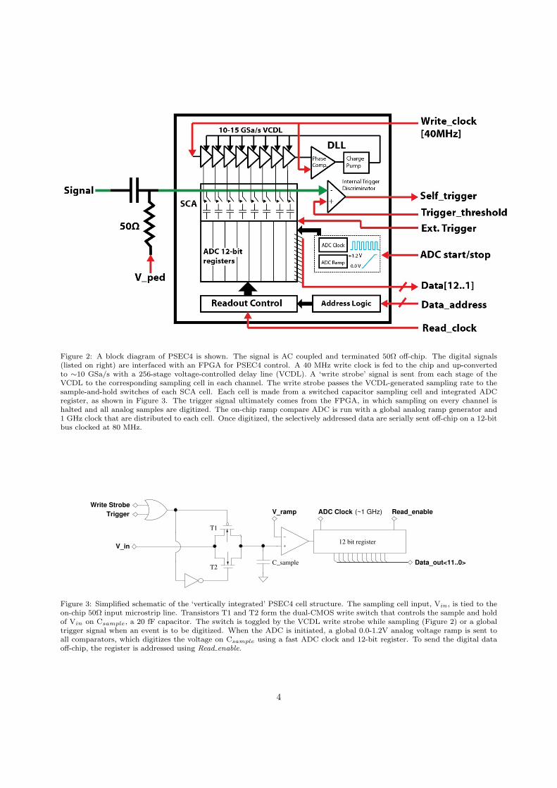
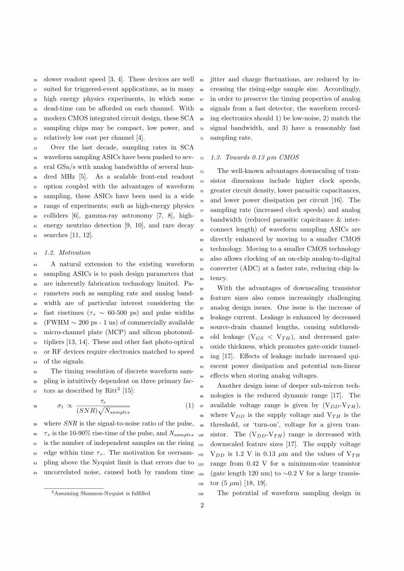
Figure 2: A block diagram of PSEC4 is shown. The signal is AC coupled and terminated 50Ω off-chip. The digital signals(listed on right) are interfaced with an FPGA for PSEC4 control. A 40 MHz write clock is fed to the chip and up-convertedto ∼10 GSa/s with a 256-stage voltage-controlled delay line (VCDL). A ‘write strobe’ signal is sent from each stage of theVCDL to the corresponding sampling cell in each channel. The write strobe passes the VCDL-generated sampling rate to thesample-and-hold switches of each SCA cell. Each cell is made from a switched capacitor sampling cell and integrated ADCregister, as shown in Figure 3. The trigger signal ultimately comes from the FPGA, in which sampling on every channel ishalted and all analog samples are digitized. The on-chip ramp compare ADC is run with a global analog ramp generator and1 GHz clock that are distributed to each cell. Once digitized, the selectively addressed data are serially sent off-chip on a 12-bitbus clocked at 80 MHz.
ADC Clock Read_enable
Data_out<11..0>
V_ramp
12 bit register
C_sample
T1
T2
(~1 GHz)Write Strobe
Trigger
V_in +
−
Figure 3: Simplified schematic of the ‘vertically integrated’ PSEC4 cell structure. The sampling cell input, Vin, is tied to theon-chip 50Ω input microstrip line. Transistors T1 and T2 form the dual-CMOS write switch that controls the sample and holdof Vin on Csample, a 20 fF capacitor. The switch is toggled by the VCDL write strobe while sampling (Figure 2) or a globaltrigger signal when an event is to be digitized. When the ADC is initiated, a global 0.0-1.2V analog voltage ramp is sent toall comparators, which digitizes the voltage on Csample using a fast ADC clock and 12-bit register. To send the digital dataoff-chip, the register is addressed using Read enable.
4

2
4
6
8
10
12
14
16
18
20
0 0.1 0.2 0.3 0.4 0.5 0.6 0.7 0.8
Sam
plin
g R
ate
[G
Sa/s
]
Voltage Control [V]
MeasuredFit to DataSimulated
Figure 4: Sampling rate as a function of VCDL voltage control. Good agreement is shown between post layout simulationand actual values. Rates up to 17 GSa/s are achieved with the free-running PSEC4 VCDL. An exponential fit describes theobserved performance [insert fit parameters].
power supply variations. The DLL is composed of172
a dual phase comparator and charge pump circuit173
to lock both the rising and falling edges of the write174
clock at a fixed one-cycle latency [22]. A loop-filter175
capacitor is installed externally to tune the DLL176
stability.177
With this architecture, a write clock with fre-178
quency fin is provided to the chip, and the sampling179
is started automatically after a locking time of sev-180
eral seconds. The nominal sampling rate [GSa/s],181
is set by 0.256·fin [MHz], and the sampling buffer182
depth [ns] is given by 103/fin [MHz−1]. A limitation183
of the PSEC4 design is the relatively small record-184
ing depth at high sampling rates due to the buffer185
size of 256 samples.186
2.2. Sampling and Triggering187
A single-ended, 256-cell SCA was designed and188
implemented on each channel of PSEC4. Each sam-189
pling cell circuit is made from a dual CMOS write190
switch and a 20 fF sampling capacitor as shown191
in Figure 3. During sampling, the write switch192
is toggled by the write strobe from the VCDL. To193
record an event, an external trigger, typically from194
an FPGA, overrides the sampling and opens all195
write switches, holding the analog voltages on the196
capacitor for the ADC duration (≤4 µs).197
PSEC4 has the capability for self-triggering. An198
internal trigger circuit, made from a fast compara-199
tor and digital logic, was included on each chan-200
nel. The trigger output bits are sent to the FPGA,201
which returns a global trigger signal back to the202
chip. Triggering interrupts the sampling on every203
channel, and is held until the selected data is digi-204
tized and read out.205
2.3. ADC206
Digital conversion of the sampled waveforms is207
done on-chip with a ramp-compare ADC that is208
parallelized over the entire ASIC. Each sample209
cell has a dedicated comparator and 12 bit reg-210
ister as shown in Figure 3. In this architec-211
ture, the comparison between each sampled voltage212
(Vsample) and a global ramping voltage (Vramp),213
controls the clocking of a 12-bit register. When214
Vramp > Vsample, the register clocking is disabled,215
and the 12-bit word, which has been encoded by the216
ADC clock frequency and the ramp duration below217
Vsample, is latched and ready for readout.218
5
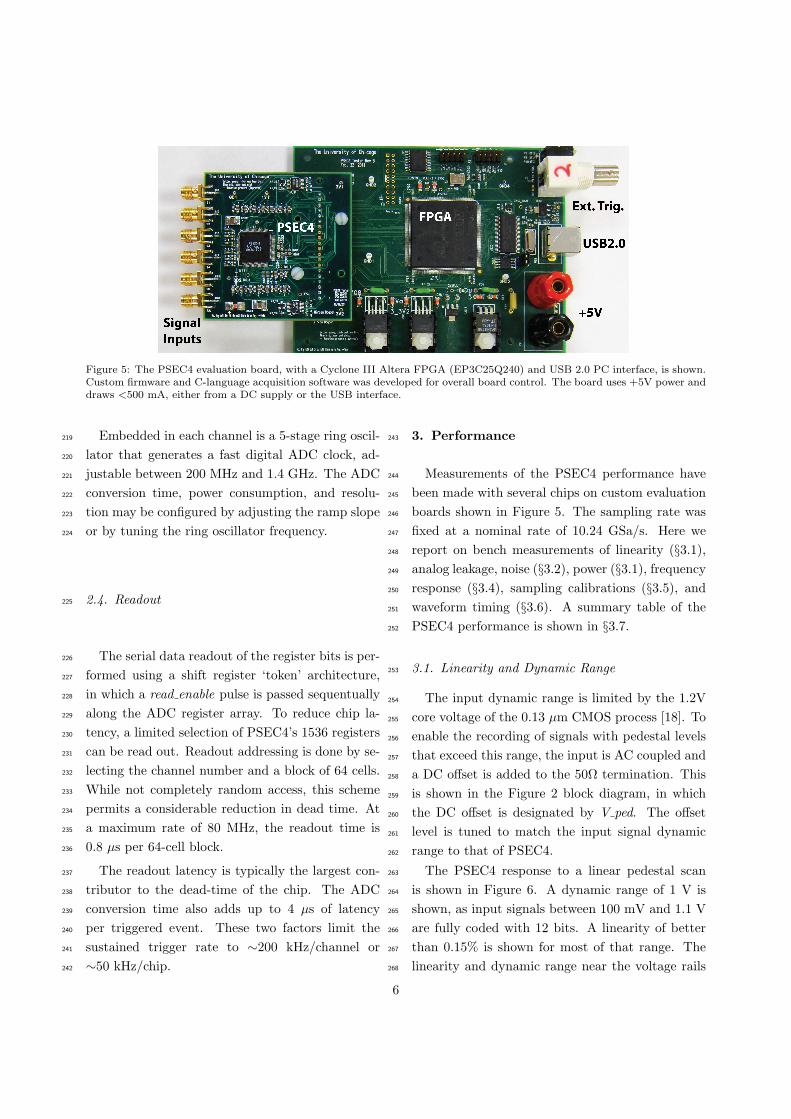
Figure 5: The PSEC4 evaluation board, with a Cyclone III Altera FPGA (EP3C25Q240) and USB 2.0 PC interface, is shown.Custom firmware and C-language acquisition software was developed for overall board control. The board uses +5V power anddraws <500 mA, either from a DC supply or the USB interface.
Embedded in each channel is a 5-stage ring oscil-219
lator that generates a fast digital ADC clock, ad-220
justable between 200 MHz and 1.4 GHz. The ADC221
conversion time, power consumption, and resolu-222
tion may be configured by adjusting the ramp slope223
or by tuning the ring oscillator frequency.224
2.4. Readout225
The serial data readout of the register bits is per-226
formed using a shift register ‘token’ architecture,227
in which a read enable pulse is passed sequentually228
along the ADC register array. To reduce chip la-229
tency, a limited selection of PSEC4’s 1536 registers230
can be read out. Readout addressing is done by se-231
lecting the channel number and a block of 64 cells.232
While not completely random access, this scheme233
permits a considerable reduction in dead time. At234
a maximum rate of 80 MHz, the readout time is235
0.8 µs per 64-cell block.236
The readout latency is typically the largest con-237
tributor to the dead-time of the chip. The ADC238
conversion time also adds up to 4 µs of latency239
per triggered event. These two factors limit the240
sustained trigger rate to ∼200 kHz/channel or241
∼50 kHz/chip.242
3. Performance243
Measurements of the PSEC4 performance have244
been made with several chips on custom evaluation245
boards shown in Figure 5. The sampling rate was246
fixed at a nominal rate of 10.24 GSa/s. Here we247
report on bench measurements of linearity (§3.1),248
analog leakage, noise (§3.2), power (§3.1), frequency249
response (§3.4), sampling calibrations (§3.5), and250
waveform timing (§3.6). A summary table of the251
PSEC4 performance is shown in §3.7.252
3.1. Linearity and Dynamic Range253
The input dynamic range is limited by the 1.2V254
core voltage of the 0.13 µm CMOS process [18]. To255
enable the recording of signals with pedestal levels256
that exceed this range, the input is AC coupled and257
a DC offset is added to the 50Ω termination. This258
is shown in the Figure 2 block diagram, in which259
the DC offset is designated by V ped. The offset260
level is tuned to match the input signal dynamic261
range to that of PSEC4.262
The PSEC4 response to a linear pedestal scan263
is shown in Figure 6. A dynamic range of 1 V is264
shown, as input signals between 100 mV and 1.1 V265
are fully coded with 12 bits. A linearity of better266
than 0.15% is shown for most of that range. The267
linearity and dynamic range near the voltage rails268
6
-20
0
20
0 0.2 0.4 0.6 0.8 1 1.2Input Voltage [V]
Fit Residuals 0
500
1000
1500
2000
2500
3000
3500
4000
PS
EC
4 o
utp
ut [A
DC
counts
]
Raw Pedestal ScanLinear fit
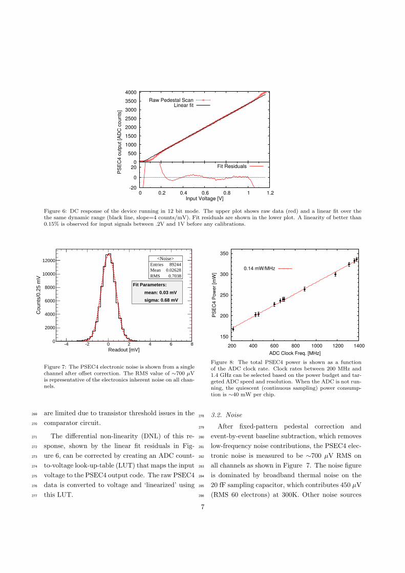
Figure 6: DC response of the device running in 12 bit mode. The upper plot shows raw data (red) and a linear fit over thethe same dynamic range (black line, slope=4 counts/mV). Fit residuals are shown in the lower plot. A linearity of better than0.15% is observed for input signals between .2V and 1V before any calibrations.
<Noise>Entries 89244Mean 0.02628RMS 0.7038
Readout [mV]-4 -2 0 2 4 6 8
Cou
nts/
0.25
mV
0
2000
4000
6000
8000
10000
12000 <Noise>Entries 89244Mean 0.02628RMS 0.7038
Fit Parameters:
mean: 0.03 mV
sigma: 0.68 mV
Figure 7: The PSEC4 electronic noise is shown from a singlechannel after offset correction. The RMS value of ∼700 µVis representative of the electronics inherent noise on all chan-nels.
are limited due to transistor threshold issues in the269
comparator circuit.270
The differential non-linearity (DNL) of this re-271
sponse, shown by the linear fit residuals in Fig-272
ure 6, can be corrected by creating an ADC count-273
to-voltage look-up-table (LUT) that maps the input274
voltage to the PSEC4 output code. The raw PSEC4275
data is converted to voltage and ‘linearized’ using276
this LUT.277
150
200
250
300
350
200 400 600 800 1000 1200 1400
PS
EC
4 P
ow
er
[mW
]
ADC Clock Freq. [MHz]
0.14 mW/MHz
Figure 8: The total PSEC4 power is shown as a functionof the ADC clock rate. Clock rates between 200 MHz and1.4 GHz can be selected based on the power budget and tar-geted ADC speed and resolution. When the ADC is not run-ning, the quiescent (continuous sampling) power consump-tion is ∼40 mW per chip.
3.2. Noise278
After fixed-pattern pedestal correction and279
event-by-event baseline subtraction, which removes280
low-frequency noise contributions, the PSEC4 elec-281
tronic noise is measured to be ∼700 µV RMS on282
all channels as shown in Figure 7. The noise figure283
is dominated by broadband thermal noise on the284
20 fF sampling capacitor, which contributes 450 µV285
(RMS 60 electrons) at 300K. Other noise sources286
7
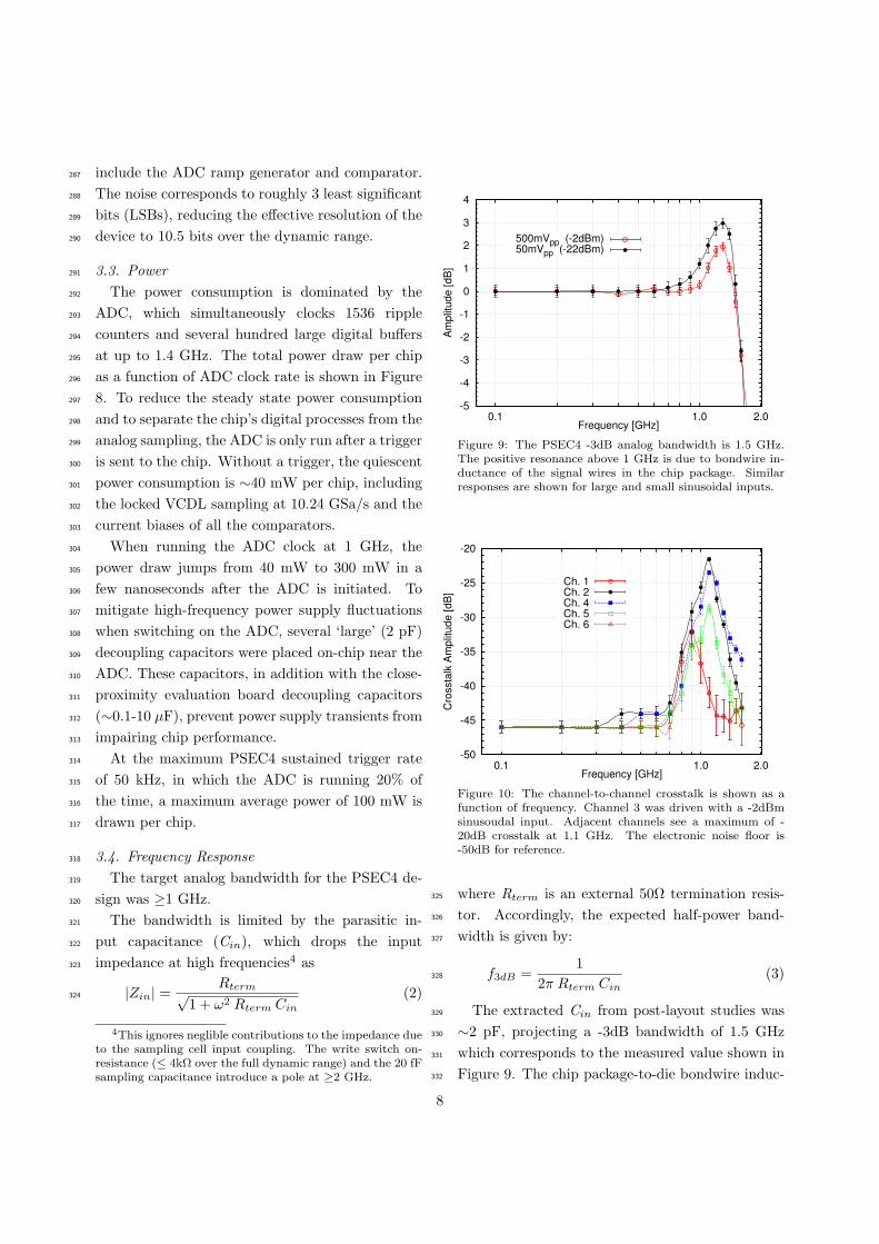
include the ADC ramp generator and comparator.287
The noise corresponds to roughly 3 least significant288
bits (LSBs), reducing the effective resolution of the289
device to 10.5 bits over the dynamic range.290
3.3. Power291
The power consumption is dominated by the292
ADC, which simultaneously clocks 1536 ripple293
counters and several hundred large digital buffers294
at up to 1.4 GHz. The total power draw per chip295
as a function of ADC clock rate is shown in Figure296
8. To reduce the steady state power consumption297
and to separate the chip’s digital processes from the298
analog sampling, the ADC is only run after a trigger299
is sent to the chip. Without a trigger, the quiescent300
power consumption is ∼40 mW per chip, including301
the locked VCDL sampling at 10.24 GSa/s and the302
current biases of all the comparators.303
When running the ADC clock at 1 GHz, the304
power draw jumps from 40 mW to 300 mW in a305
few nanoseconds after the ADC is initiated. To306
mitigate high-frequency power supply fluctuations307
when switching on the ADC, several ‘large’ (2 pF)308
decoupling capacitors were placed on-chip near the309
ADC. These capacitors, in addition with the close-310
proximity evaluation board decoupling capacitors311
(∼0.1-10 µF), prevent power supply transients from312
impairing chip performance.313
At the maximum PSEC4 sustained trigger rate314
of 50 kHz, in which the ADC is running 20% of315
the time, a maximum average power of 100 mW is316
drawn per chip.317
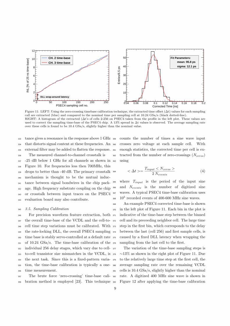
3.4. Frequency Response318
The target analog bandwidth for the PSEC4 de-319
sign was ≥1 GHz.320
The bandwidth is limited by the parasitic in-321
put capacitance (Cin), which drops the input322
impedance at high frequencies4 as323
|Zin| =Rterm√
1 + ω2 Rterm Cin
(2)324
4This ignores neglible contributions to the impedance dueto the sampling cell input coupling. The write switch on-resistance (≤ 4kΩ over the full dynamic range) and the 20 fFsampling capacitance introduce a pole at ≥2 GHz.
-5
-4
-3
-2
-1
0
1
2
3
4
0.1 1.0 2.0
Am
plit
ude [dB
]
Frequency [GHz]
500mVpp (-2dBm)50mVpp (-22dBm)
Figure 9: The PSEC4 -3dB analog bandwidth is 1.5 GHz.The positive resonance above 1 GHz is due to bondwire in-ductance of the signal wires in the chip package. Similarresponses are shown for large and small sinusoidal inputs.
-50
-45
-40
-35
-30
-25
-20
0.1 1.0 2.0
Cro
ssta
lk A
mplit
ude [dB
]
Frequency [GHz]
Ch. 1Ch. 2Ch. 4Ch. 5Ch. 6
Figure 10: The channel-to-channel crosstalk is shown as afunction of frequency. Channel 3 was driven with a -2dBmsinusoudal input. Adjacent channels see a maximum of -20dB crosstalk at 1.1 GHz. The electronic noise floor is-50dB for reference.
where Rterm is an external 50Ω termination resis-325
tor. Accordingly, the expected half-power band-326
width is given by:327
f3dB =1
2π Rterm Cin(3)328
The extracted Cin from post-layout studies was329
∼2 pF, projecting a -3dB bandwidth of 1.5 GHz330
which corresponds to the measured value shown in331
Figure 9. The chip package-to-die bondwire induc-332
8
PSEC4 sampling cell no.0 50 100 150 200 250
INL
[% o
f 25
ns ti
me-
base
]
0
2
4
6
8
10
12
CH. 2 time-base
CH. 3 time-base
DLL wrap-around latency
Corrected Time [ns]0.04 0.06 0.08 0.1 0.12 0.14 0.16 0.18 0.2
Ent
ries/
6.5
ps
0
10
20
30
40
50 Fit Parameters:mean: 95.8 ps
sigma: 12.1 ps
Figure 11: LEFT: Using the zero-crossing timebase calibration technique, the extracted time offset (∆t) values for each samplingcall are extracted (blue) and compared to the nominal time per sampling cell at 10.24 GSa/s (black dotted-line).RIGHT: A histogram of the extracted (∆t’s of cells 2-256 on PSEC4 taken from the profile in the left plot. These values areused to correct the sampling time-base of the PSEC4 chip. A 13% spread in ∆t values is observed. The average sampling rateover these cells is found to be 10.4 GSa/s, slightly higher than the nominal value.
tance gives a resonance in the response above 1 GHz333
that distorts signal content at these frequencies. An334
external filter may be added to flatten the response.335
The measured channel-to-channel crosstalk is336
-25 dB below 1 GHz for all channels as shown in337
Figure 10. For frequencies less then 700MHz, this338
drops to better than -40 dB. The primary crosstalk339
mechanism is thought to be the mutual induc-340
tance between signal bondwires in the chip pack-341
age. High frequency substrate coupling on the chip342
or crosstalk between input traces on the PSEC4343
evaluation board may also contribute.344
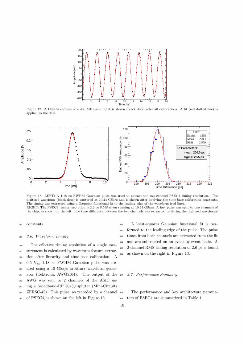
3.5. Sampling Calibration345
For precision waveform feature extraction, both346
the overall time-base of the VCDL and the cell-to-347
cell time step variations must be calibrated. With348
the rate-locking DLL, the overall PSEC4 sampling349
time base is stably servo-controlled at a default rate350
of 10.24 GSa/s. The time-base calibration of the351
individual 256 delay stages, which vary due to cell-352
to-cell transistor size mismatches in the VCDL, is353
the next task. Since this is a fixed-pattern varia-354
tion, the time-base calibration is typically a one-355
time measurement.356
The brute force ‘zero-crossing’ time-base cali-357
bration method is employed [23]. This technique358
counts the number of times a sine wave input359
crosses zero voltage at each sample cell. With360
enough statistics, the corrected time per cell is ex-361
tracted from the number of zero-crossings (Nzeros)362
using363
< ∆t >=Tinput < Nzeros >
2Nevents(4)364
where Tinput is the period of the input sine365
and Nevents is the number of digitized sine366
waves. A typical PSEC4 time-base calibration uses367
105 recorded events of 400-600 MHz sine waves.368
An example PSEC4 corrected time-base is shown369
in the left plot of Figure 11. Each bin in the plot is370
indicative of the time-base step between the binned371
cell and its preceeding neighbor cell. The large time372
step in the first bin, which corresponds to the delay373
between the last (cell 256) and first sample cells, is374
caused by a fixed DLL latency when wrapping the375
sampling from the last cell to the first.376
The variation of the time-base sampling steps is377
∼13% as shown in the right plot of Figure 11. Due378
to the relatively large time step at the first cell, the379
average sampling rate over the remaining VCDL380
cells is 10.4 GSa/s, slightly higher than the nominal381
rate. A digitized 400 MHz sine wave is shown in382
Figure 12 after applying the time-base calibration383
9
Time [ns]0 2 4 6 8 10 12 14 16 18 20
Am
plitu
de [m
V]
-200
-150
-100
-50
0
50
100
150
200
Figure 12: A PSEC4 capture of a 400 MHz sine input is shown (black dots) after all calibrations. A fit (red dotted line) isapplied to the data.
Time [ns]0 2 4 6 8 10
Am
plitu
de [V
]
0
0.05
0.1
0.15
0.2
0.25 t_diffEntries 1595Mean 200.1RMS 2.579
Time Difference [ps]190 195 200 205 210 215 220 225
Ent
ries/
750
fem
tose
cond
s
0
20
40
60
80
100
120t_diff
Entries 1595Mean 200.1RMS 2.579
Fit Parameters:
mean: 200.0 ps
sigma: 2.55 ps
Figure 13: LEFT: A 1.18 ns FWHM Gaussian pulse was used to extract the two-channel PSEC4 timing resolution. Thedigitized waveform (black dots) is captured at 10.24 GSa/s and is shown after applying the time-base calibration constants.The timing was extracted using a Gaussian-functional fit to the leading edge of the waveform (red line).RIGHT: The PSEC4 timing resolution is 2.6 ps RMS when running at 10.24 GSa/s. A fast pulse was split to two channels ofthe chip, as shown on the left. The time difference between the two channels was extracted by fitting the digitized waveforms
constants.384
3.6. Waveform Timing385
The effective timing resolution of a single mea-386
surement is calculated by waveform feature extrac-387
tion after linearity and time-base calibration. A388
0.5 Vpp 1.18 ns FWHM Gaussian pulse was cre-389
ated using a 10 GSa/s arbitrary waveform gener-390
ator (Tektronix AWG5104). The output of the391
AWG was sent to 2 channels of the ASIC us-392
ing a broadband-RF 50/50 splitter (Mini-Circuits393
ZFRSC-42). This pulse, as recorded by a channel394
of PSEC4, is shown on the left in Figure 13.395
A least-squares Gaussian functional fit is per-396
formed to the leading edge of the pulse. The pulse397
times from both channels are extracted from the fit398
and are subtracted on an event-by-event basis. A399
2-channel RMS timing resolution of 2.6 ps is found400
as shown on the right in Figure 13.401
3.7. Performance Summary402
The performance and key architecture parame-403
ters of PSEC4 are summarized in Table 1.404
10
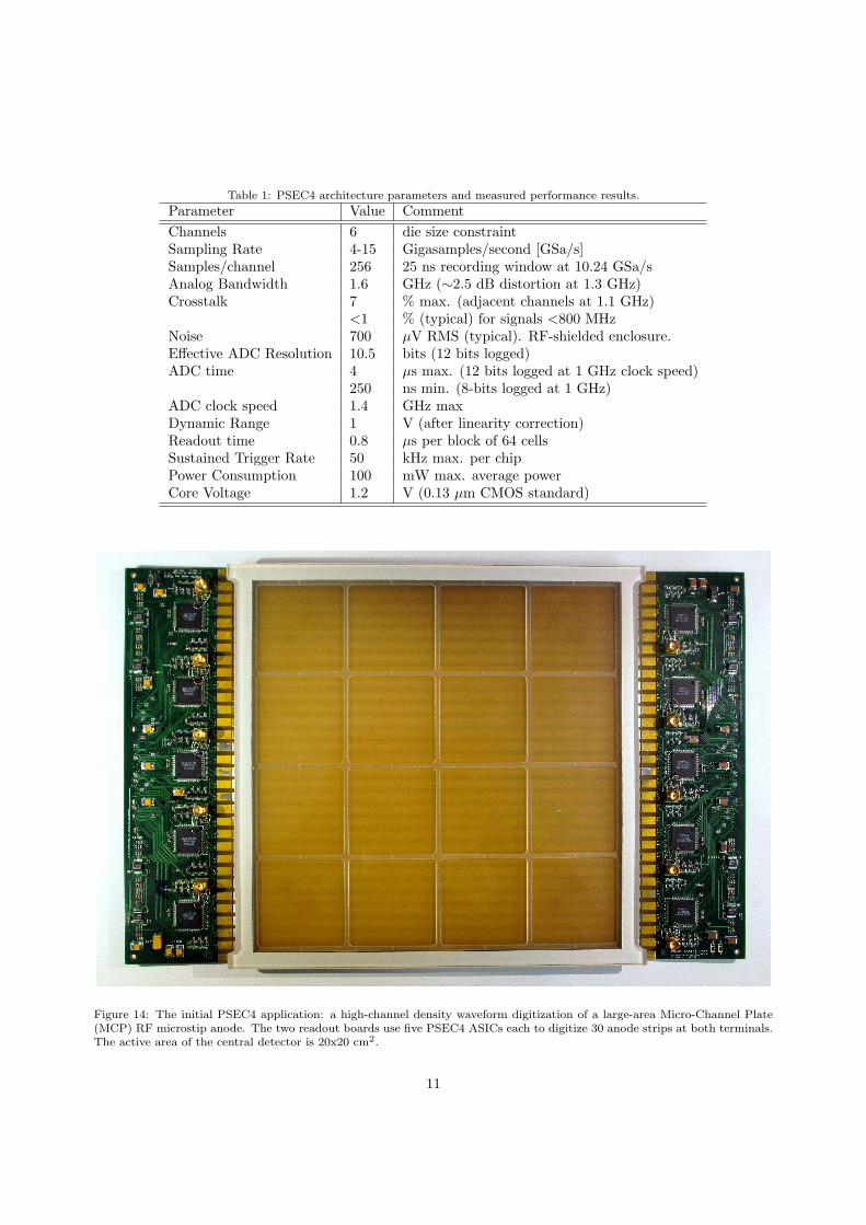
Table 1: PSEC4 architecture parameters and measured performance results.
Parameter Value CommentChannels 6 die size constraintSampling Rate 4-15 Gigasamples/second [GSa/s]Samples/channel 256 25 ns recording window at 10.24 GSa/sAnalog Bandwidth 1.6 GHz (∼2.5 dB distortion at 1.3 GHz)Crosstalk 7 % max. (adjacent channels at 1.1 GHz)
<1 % (typical) for signals <800 MHzNoise 700 µV RMS (typical). RF-shielded enclosure.Effective ADC Resolution 10.5 bits (12 bits logged)ADC time 4 µs max. (12 bits logged at 1 GHz clock speed)
250 ns min. (8-bits logged at 1 GHz)ADC clock speed 1.4 GHz maxDynamic Range 1 V (after linearity correction)Readout time 0.8 µs per block of 64 cellsSustained Trigger Rate 50 kHz max. per chipPower Consumption 100 mW max. average powerCore Voltage 1.2 V (0.13 µm CMOS standard)
Figure 14: The initial PSEC4 application: a high-channel density waveform digitization of a large-area Micro-Channel Plate(MCP) RF microstip anode. The two readout boards use five PSEC4 ASICs each to digitize 30 anode strips at both terminals.The active area of the central detector is 20x20 cm2.
11
4. Application to Large-Area Photodetec-405
tors406
The first application of PSEC4 is the front-end407
waveform digitization of large-area photodetectors408
with picosecond-level time resolution [24, 25]. The409
LAPPD MCP-PMT is a 20 x 20 cm2 (8 x 8 in2) her-410
metically packaged photodetector with a 30 chan-411
nel RF microstrip anode signal pick-off [26]. The412
1-dimensional trasmission line anode design is opti-413
mized for precise spatial resolution with an effecient414
use of electronics channels. The (x,y) position of415
the incident particle or photon is extracted by us-416
ing the differential times of waveforms at the two417
microstrip terminals (x), and the relative charge418
captured on neighboring strips (y) [26]. Waveform419
sampling, matched to the MCP bandwidth, allows420
for both the time and charge extraction to deter-421
mine the (x,y) position, in addition to the time-of-422
arrival and energy of the incident particle or pho-423
ton.424
A compact, detector integrated data acquisition425
(DAQ) system was designed for the LAPPD MCP-426
PMTs. The front-end microstrip anode waveform427
digitization board shown in Figure 14, in which five428
PSEC4 ASICS are used on each end to capture429
waveforms from all 30 strips. The board maintains430
a 50Ω impedance between the anode output and431
the chip input. The back-end FPGA and clock-432
distribution boards (not shown) can be mechani-433
cally mounted behind the LAPPD MCP-PMT.434
The ‘single-tile’ readout configuration is shown435
in Figure 14 . Depending on the application event436
rate, the detector active area may be increased by437
serially connecting the microstrip anodes of adja-438
cent LAPPD MCP tiles using a common front-end439
PSEC4 digitizer board and DAQ system [26].440
5. Conclusion441
We have described the architecture and perfor-442
mance of the PSEC4 waveform digitzing ASIC. The443
advantages of implementing waveform sampling IC444
design in a deeper sub-micron process were shown,445
with sampling rates of 15 GSa/s and analog band-446
widths of 1.5 GHz achieved. Potential 0.13 µm447
design issues, such as leakage and dynamic range,448
were optimized and provide a 1 V dynamic range449
with sub-mV electronics noise. A one-time time-450
base calibration is required to get precise waveform451
timing with 2-3 picosecond resolution. The first452
application of the PSEC4 ASIC is the compact,453
low power front-end waveform sampling of LAPPD454
MCP-PMTs.455
6. Acknowledgements456
We thank Mircea Bogdan, Fukun Tang, Mark Za-457
skowski, and Mary Heintz for their strong support458
in the Electronics Development Group of the En-459
rico Fermi Institute. Stefan Ritt, Eric Delagnes,460
and Dominique Breton provided invaluable guid-461
ance and advice on SCA chips.462
This work is supported by the Department of En-463
ergy, Contract No. DE-AC02-06CH11357, and the464
National Science Foundation, Grant No. PHY-106465
601 4.466
References467
[1] J.-F. Genat, G. Varner, F. Tang, H.J. Frisch, Nucl. In-468
str. Meth. A 607 (2009) 387-393.469
[2] D. Breton, E. Delagnes, J. Maalmi, K. Nishimura, L.L.470
Ruckman, G. Varner, J. Va’vra, Nucl. Instr. Meth A471
629 (2011) 123.472
[3] S. Kleinfelder, IEEE Trans. Nucl. Sci. 35, (1988) 151.473
[4] G. Haller, B. Wooley, “A 700 MHz Switched Capacitor474
Analog Waveform Sampling Circuit”, SLAC-PUB-6414475
(1993).476
[5] S. Ritt, “Gigahertz Waveform Sampling: An Overview477
and Outlook”, 12th Pisa Meeting on Advanced Detec-478
tors, 23 May 2012.479
[6] G.S. Varner, L.L Ruckman, J.W. Nam, R.J. Nichol, J.480
Cao, P.W. Gorham, M. Wilcox, Nucl. Instr. Meth. A481
583 (2007) 447-460.482
[7] E. Delagnes, Y. Degerli, P. Goret, P. Nayman, F. Tou-483
ssenel, P. Vincent, Nucl. Instr. Meth. A 567 (2006) 21.484
[8] K. Bechtol, S. Funk, A. Okumra, L. Ruckman, A. si-485
mons, H. Tajima, J. Vandenbroucke, G. Varner, J. As-486
troparticle Physics 36 (2012) 156.487
[9] S. Kleinfelder, IEEE Trans. Nucl. Sci. 50, (2003) 955.488
[10] G.S. Varner, P. Gorham, J. Cao, Proc. SPIE Int. Soc.489
Opt. Eng 4858 (2003) 31.490
12
[11] C. Broennimann, R. Horisberger, R. Schnyder, Nucl.491
Instr. Meth. A 420 (1999) 264-269.492
[12] S. Ritt, Nucl. Instr. Meth. A 518 (2004) 470-471.493
[13] J. Milnes, J. Howorth, “Picosecond Time Response494
Characteristics of Micro-channel Plate PMT Detec-495
tors”, SPIE USE, V. 8 5580 (2004) 89.496
[14] P. Eraerds, M. Legre, A. Rochas, H. Zbinden, N. Gisin,497
“SiPM for fast Photon-Counting and Multiphoton De-498
tection”, Optics Express, Vol. 15 (2007) 14539.499
[15] S. Ritt, “The Role of Analog Bandwidth and500
S/N in Timing”, talk at The Factors that501
Limit Timing Resolution in Photodetectors,502
<http://psec.uchicago.edu/workshops/503
fast timing conf 2011/>, University of Chicago, Apr504
2011.505
[16] R.H. Dennard, F. H. Gaennsslen, H. N. Yu, V.L506
Rideout, E. Bassous, A.R. LeBlanc, “Design of Ion-507
Implemented MOSFETs with Very Small Physical Di-508
mensions,” IEEE J. Solid-State Circuits SC-9 (1974)509
256.510
[17] Y. Taur et. al., “CMOS Scaling into the Nanometer511
Regime”, Proc. IEEE. Vol. 85, No. 4, (1997).512
[18] IBM Corporation, “CMRF8SF Model Reference513
Guide”, V.1.4.0.10 (2008).514
[19] The MOSIS Service. Wafer Electrical Test Data and515
SPICE Model Parameters. Run: V18B. Available516
on-line (accessed 4 Feb. 2013):517
<http:://www.mosis.com/pages/Technical/518
Testdata/ibm-013-prm>519
[20] E. Oberla, H. Grabas, M. Bogdan, H. Frisch, J.-F.520
Genat, K. Nishimura, G. Varner, A. Wong, “A 4-521
Channel Waveform Sampling ASIC in 0.13 µm CMOS522
for Front-End Readout of Large-Area Micro-Channel523
Plate Detectors”, Physics Procedia 37 (2012) 1690-524
1698.525
[21] M. Cooney, M. Andrew, K. Nishimura, L. Ruckman,526
G. Varner, H. Grabas, E. Oberla, J.-F. Genat, “Multi-527
purpose Test Structures and Process Characterization528
using 0.13 µm CMOS: The CHAMP ASIC”, Physics529
Procedia 37 (2012) 1707-1714.530
[22] H. Chang et al., “A Wide-Range Delay-Locked Loop531
With a Fixed Latency of One Clock Cycle”, IEEE J.532
Solid-State Circuits 37 (2002) 1021.533
[23] K. Nishimura, A. Romero-Wolf, “A Correlation-Based534
Timing Calibration & Diagnostic Technique for Fast535
Digitization ASICs”, Physics Procedia 37 (2012) 1707-536
1714.537
[24] The Large-Area Picosecond Photo-Detectors Project538
web page: <http://psec.uchicago.edu>539
[25] M. Wetstein, B. Adams, A. Elagin, J. Elam, H. Frisch,540
Z. Insepov, V. Ivanov, S. Jokela, A. Mane, R. Obaid, I.541
Veryovkin, A. Vostrikov, R. Wagner, A. Zinovev et al.,542
to be submitted to Nucl. Instr. Meth. A (2013).543
[26] H. Grabas, R. Obaid, E. Oberla, H. Frisch, et. al., “RF544
Strip-Line Anodes for Psec Large-Area MCP-based545
Photodetectors”, to be published Nucl. Instr. Meth. A546
(2013).547
13