wp6: graphene spintronicsgraphene.sciencesconf.org/conference/graphene/pages/7_fert.pdf · wp6:...
TRANSCRIPT
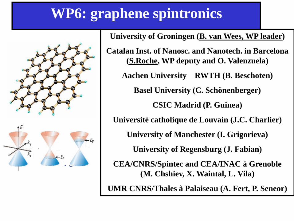
WP6: graphene spintronics
University of Groningen (B. van Wees, WP leader)
Catalan Inst. of Nanosc. and Nanotech. in Barcelona
(S.Roche, WP deputy and O. Valenzuela)
Aachen University – RWTH (B. Beschoten)
Basel University (C. Schönenberger)
CSIC Madrid (P. Guinea)
Université catholique de Louvain (J.C. Charlier)
University of Manchester (I. Grigorieva)
University of Regensburg (J. Fabian)
CEA/CNRS/Spintec and CEA/INAC à Grenoble
(M. Chshiev, X. Waintal, L. Vila)
UMR CNRS/Thales à Palaiseau (A. Fert, P. Seneor)
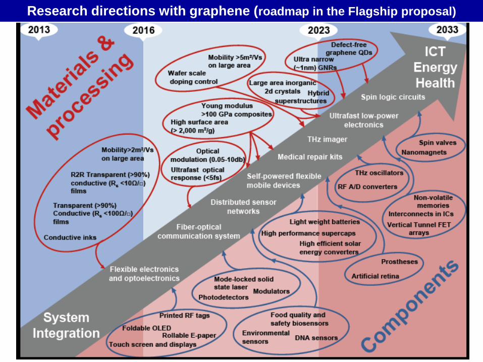
Research directions with graphene (roadmap in the Flagship proposal)
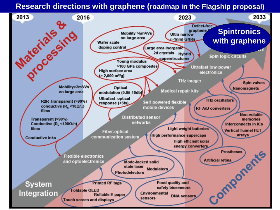
Spintronics
with graphene
Research directions with graphene (roadmap in the Flagship proposal)

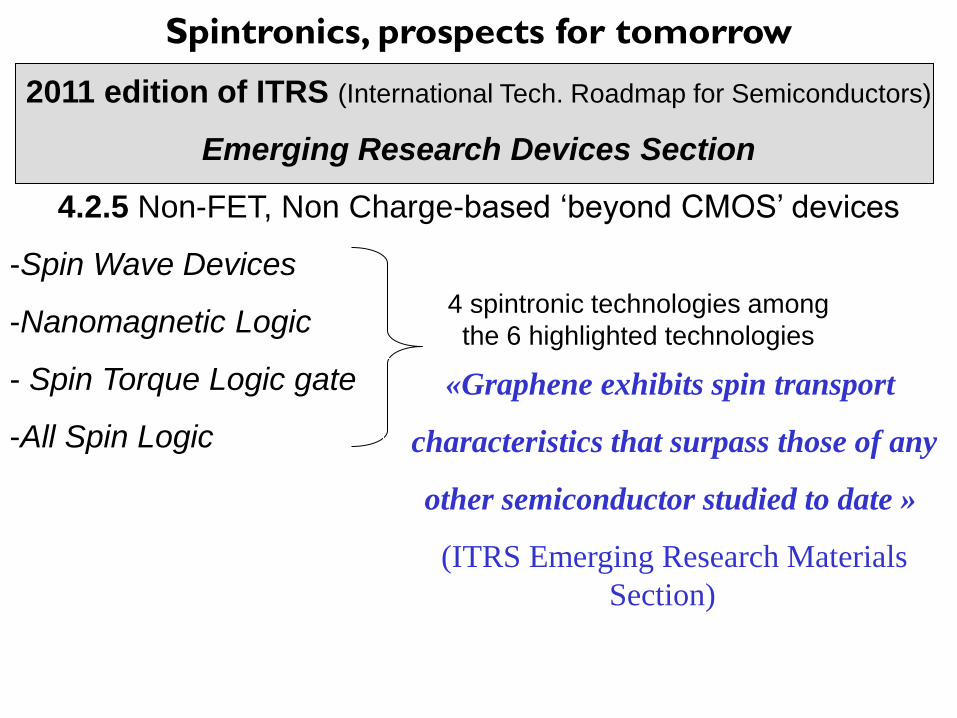
Spintronics, prospects for tomorrow
2011 edition of ITRS (International Tech. Roadmap for Semiconductors)
Emerging Research Devices Section
6.5 Memory and Logic Technologies for Accelerated Development
– STT-RAM is one the 3 technologies to be developed in an
accelerated way (to replace RAM or MRAM with advantages
in terms of bit density,power dissipation, CMOS integration)
4.2.5 Non-FET, Non Charge-based ‘beyond CMOS’ devices
-Spin Wave Devices
-Nanomagnetic Logic
- Spin Torque Logic gate
-All Spin Logic
4 spintronic technologies
among the 6 technologies put
forward for non Charge-based
‘beyond CMOS’ devices
Spintronics, prospects for tomorrow
2011 edition of ITRS (International Tech. Roadmap for Semiconductors)
Emerging Research Devices Section
4.2.5 Non-FET, Non Charge-based ‘beyond CMOS’ devices
-Spin Wave Devices
-Nanomagnetic Logic
- Spin Torque Logic gate
-All Spin Logic
4 spintronic technologies among
the 6 highlighted technologies
«Graphene exhibits spin transport
characteristics that surpass those of any
other semiconductor studied to date »
(ITRS Emerging Research Materials
Section)

Spintronics, prospects for tomorrow
2011 edition of ITRS (International Tech. Roadmap for Semiconductors)
Emerging Research Devices Section
4.2.5 Non-FET, Non Charge-based ‘beyond CMOS’ devices
-Spin Wave Devices
-Nanomagnetic Logic
- Spin Torque Logic gate
-All Spin Logic
4 spintronic technologies among
the 6 highlighted technologies
«Graphene exhibits spin transport
characteristics that surpass those of
anyother semiconductor studied to date »
Spin gates pure spin current (zero charge current)
Pure spin currents
Courtesy C. Chappert
Information coded by pure
spin currents and processed
by logic gates acting on the
spin polarization
Spin “only”
processing unit
array of
spin injectors
array of spin
detectors
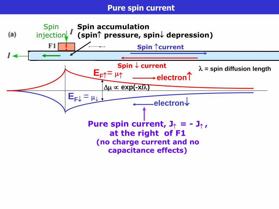
Pure spin current, J = - J , at the right of F1
(no charge current and no capacitance effects)
Spin injection
Spin current
Spin current
Spin accumulation (spin pressure, spin depression)
Pure spin current
EF=
EF =
electron
electron
= spin diffusion length
exp(-x/)

Transport and processing of
information (logic gates, etc) coded by
the polarization of pure spin currents ?
Pure spin current, J = - J , in N at the right of F1
(no charge current and no capacitance effects)
Spin injection
Spin current
Spin current
Spin “only”
processing unit
array of
spin injectors
array of
spin detectors
Courtesy C. Chappert
Pure spin current-based transport and processing of information ?
Large number of spin gates within a
spin propagation length 100 m
Spin accumulation (spin pressure, spin depression)

Quantum computing
with spins in graphene
(Loss et al) Graphene-based universal
logic gate (Dery et al, 2011)
Spintronic logic devices
based on spin transport in
a lateral channel between
spin-polarized electrodes
All spin logic with memory
B. Behin-Aein et al, 2010
Spin “only”
processing unit
array of
spin injectors
array of spin
detectors

Expected advantges of graphene for spintronic devices
1) slow spin relaxation (due to
small spin-orbit coupling, ..)
+ large velocity
long spin diffusion length
10-100 m
2) the sensitivity of the
electronic properties to
adatoms, interfaces,
impurities, edges, defects…..
can be used
for spin gating

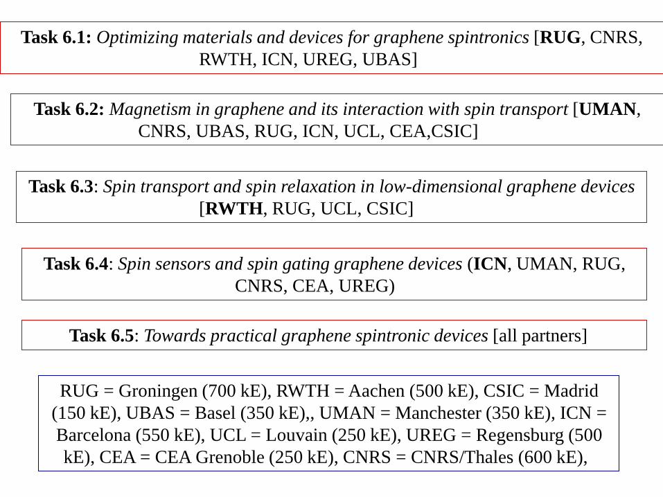
Task 6.1: Optimizing materials and devices for graphene spintronics [RUG, CNRS,
RWTH, ICN, UREG, UBAS]
Task 6.3: Spin transport and spin relaxation in low-dimensional graphene devices
[RWTH, RUG, UCL, CSIC]
Task 6.4: Spin sensors and spin gating graphene devices (ICN, UMAN, RUG,
CNRS, CEA, UREG)
Task 6.5: Towards practical graphene spintronic devices [all partners]
RUG = Groningen, RWTH = Aachen, CSIC = Madrid, UBAS =Basel,
UMAN = Manchester, ICN = Barcelona, UCL = Louvain, UREG =
Regensburg, CEA = CEA Grenoble, CNRS = CNRS/Thales,
Task 6.2: Magnetism in graphene and its interaction with spin transport [UMAN,
CNRS, UBAS, RUG, ICN, UCL, CEA,CSIC]
Task 6.1: Optimizing materials and devices for graphene spintronics [RUG, CNRS,
RWTH, ICN, UREG, UBAS]
The objective of this task is to clarify and understand the physical mechanisms which
determine the spin relaxation time and spin relaxation length in high quality graphene
devices…
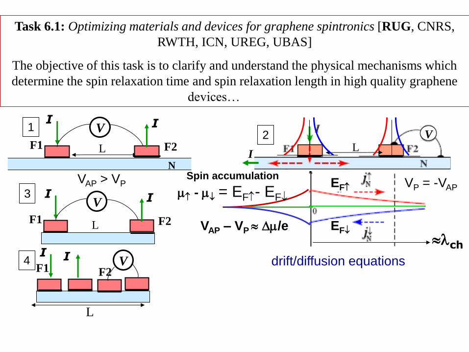
Task 6.1: Optimizing materials and devices for graphene spintronics [RUG, CNRS,
RWTH, ICN, UREG, UBAS]
The objective of this task is to clarify and understand the physical mechanisms which
determine the spin relaxation time and spin relaxation length in high quality graphene
devices…
L I
V I I
F1 F2 L
1 2
N
V
Spin accumulation
- = EF- EF
L
V I I
F1 F2
3 VP = -VAP
VAP > VP
VAP – VP /e
ch
EF
EF
drift/diffusion equations V I I
F1 F2
L
4
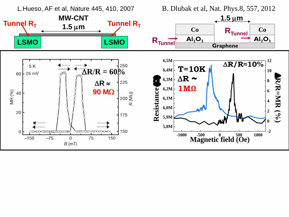
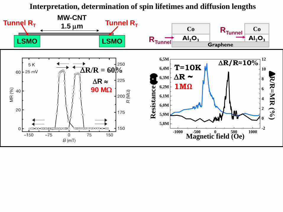
Al2O3
Co
Al2O3
Co
Graphene RTunnel
R/R≈10%
R ~
1MΩ
T=10K
-1000 -500 0 500 1000
5,8M
5,9M
6,0M
6,1M
6,2M
6,3M
6,4M
6,5M
R
/R=
MR
(%)
Resi
sta
nce
Magnetic field (Oe)
-2
0
2
4
6
8
10
12
LSMO LSMO
MW-CNT
1.5 m Tunnel RT Tunnel RT
RTunnel
R/R = 60%
R
90 M
L.Hueso, AF et al, Nature 445, 410, 2007 B. Dlubak et al, Nat. Phys.8, 557, 2012
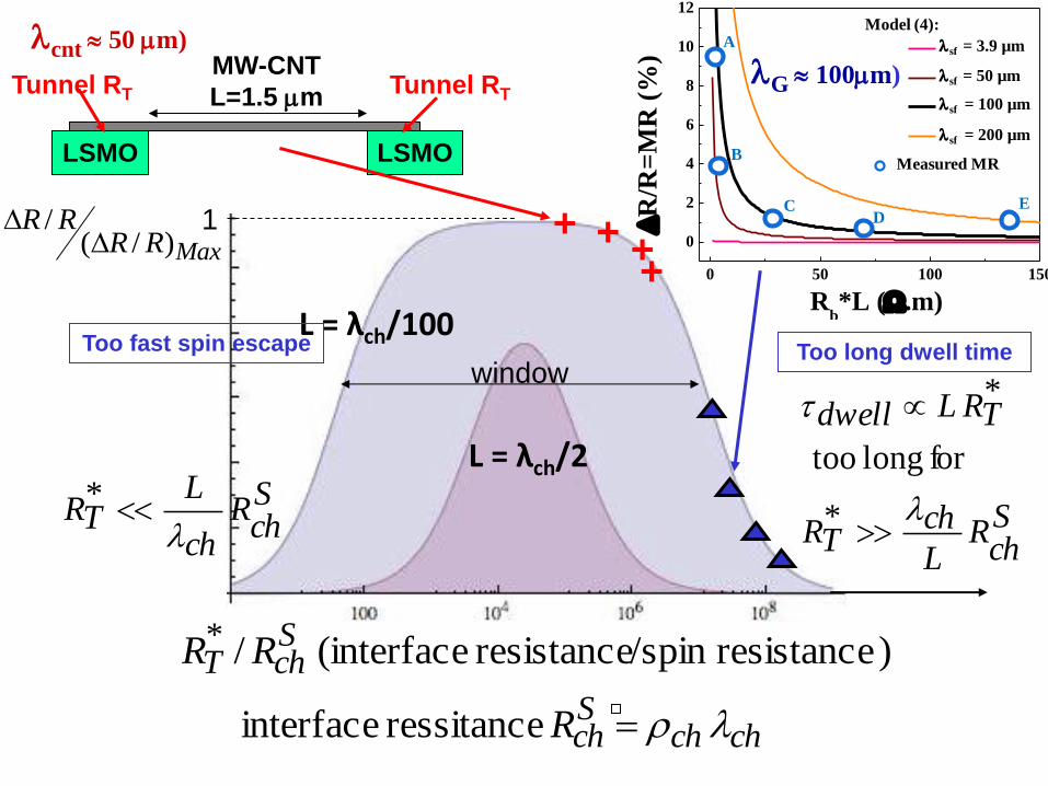
1.5 m

Al2O3
Co
Al2O3
Co
Graphene RTunnel LSMO LSMO
MW-CNT
L=1.5 m Tunnel RT Tunnel RT
RTunnel
+
+ + +
window
L = λch/100
L = λch/2
Too long dwell time Too fast spin escape
Sch
RL
chTR
TRLdwell
*
for long too
*
+
chchSch
SchT
R
RR
ressitance interface
) resistance/spin resistance interface(/*
Sch
Rch
LTR
*
RR /
MaxRRRR
)/(/
1
L.Hueso, AF et al, Nature 445, 410, 2007 B. Dlubak et al, Nat. Phys.8, 557, 2012
LSMO LSMO
MW-CNT
L=1.5 m Tunnel RT Tunnel RT
+
+ + +
window
L = λch/100
L = λch/2
Too long dwell time Too fast spin escape
Sch
RL
chTR
TRLdwell
*
for long too
*
+
chchSch
SchT
R
RR
ressitance interface
) resistance/spin resistance interface(/*
Sch
Rch
LTR
*
0 50 100 150
0
2
4
6
8
10
12
R
/R=
MR
(%
)
Rb*L (.m)
sf = 100 µm
Measured MR
A
B
CD
E
sf = 200 µm
Model (4):
sf = 3.9 µm
sf = 50 µmG 100m)
cnt 50 m)
MaxRRRR
)/(/
1
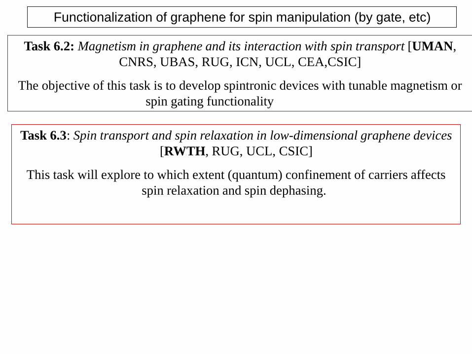
Task 6.2: Magnetism in graphene and its interaction with spin transport [UMAN,
CNRS, UBAS, RUG, ICN, UCL, CEA,CSIC]
The objective of this task is to develop spintronic devices with tunable magnetism or
spin gating functionality
Task 6.3: Spin transport and spin relaxation in low-dimensional graphene devices
[RWTH, RUG, UCL, CSIC]
This task will explore to which extent (quantum) confinement of carriers affects
spin relaxation and spin dephasing.
Functionalization of graphene for spin manipulation (by gate, etc)

Magnetism and
spin splitting
induced by
vacancies
(nanomeshes)
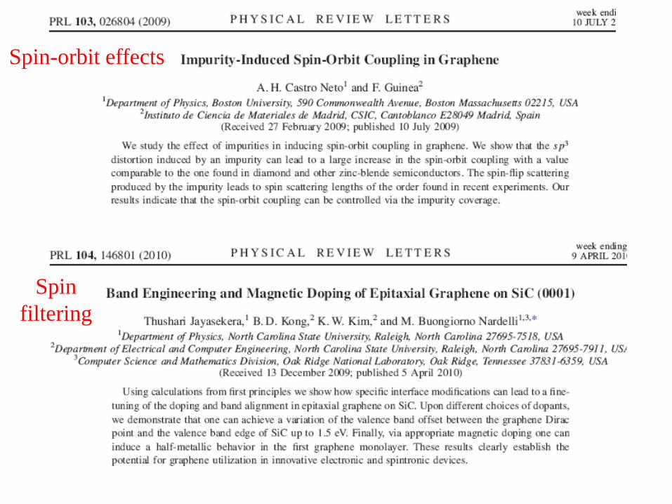
Spin-orbit effects
Spin
filtering

Task 6.4: Spin sensors and spin gating graphene devices (ICN, UMAN, RUG,
CNRS, CEA, UREG)
Task 6.5: Towards practical graphene spintronic devices [all partners]
I I
F1 F2
spin gate
source drain
Task 6.1: Optimizing materials and devices for graphene spintronics [RUG, CNRS,
RWTH, ICN, UREG, UBAS]
Task 6.3: Spin transport and spin relaxation in low-dimensional graphene devices
[RWTH, RUG, UCL, CSIC]
Task 6.4: Spin sensors and spin gating graphene devices (ICN, UMAN, RUG,
CNRS, CEA, UREG)
Task 6.5: Towards practical graphene spintronic devices [all partners]
RUG = Groningen (700 kE), RWTH = Aachen (500 kE), CSIC = Madrid
(150 kE), UBAS = Basel (350 kE),, UMAN = Manchester (350 kE), ICN =
Barcelona (550 kE), UCL = Louvain (250 kE), UREG = Regensburg (500
kE), CEA = CEA Grenoble (250 kE), CNRS = CNRS/Thales (600 kE),
Task 6.2: Magnetism in graphene and its interaction with spin transport [UMAN,
CNRS, UBAS, RUG, ICN, UCL, CEA,CSIC]

Merci pour votre attention
Al2O3
Co
Al2O3
Co
Graphene RTunnel
R/R≈10%
R ~
1MΩ
T=10K
-1000 -500 0 500 1000
5,8M
5,9M
6,0M
6,1M
6,2M
6,3M
6,4M
6,5M
R
/R=
MR
(%)
Resi
sta
nce
Magnetic field (Oe)
-2
0
2
4
6
8
10
12
LSMO LSMO
MW-CNT
1.5 m Tunnel RT Tunnel RT
RTunnel
Interpretation, determination of spin lifetimes and diffusion lengths
R/R = 60%
R
90 M
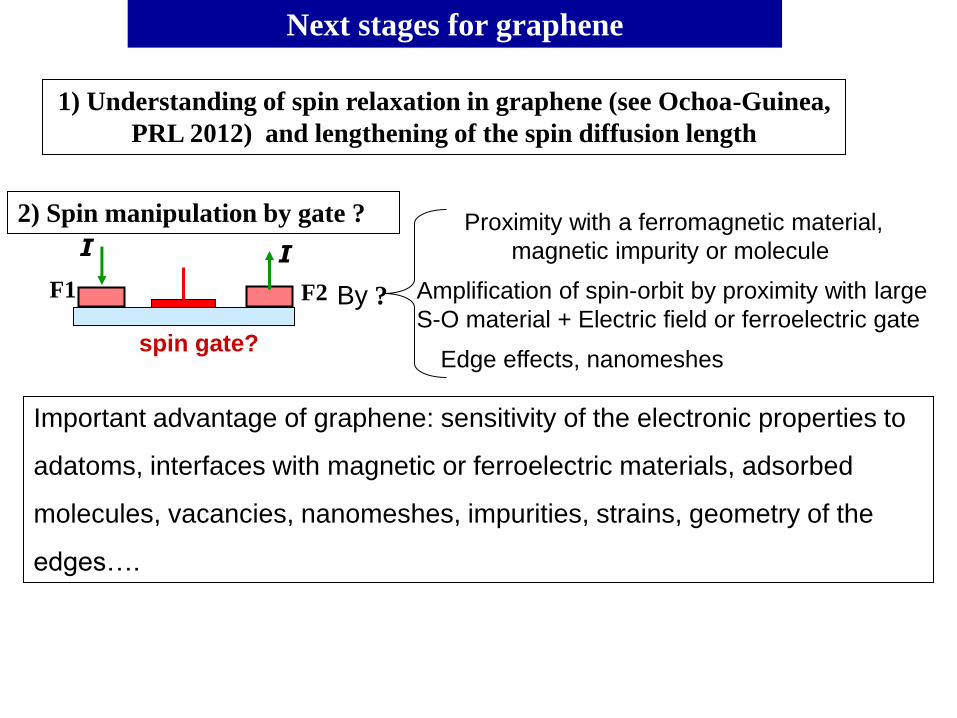
Next stages for graphene
2) Spin manipulation by gate ?
I I
F1 F2
spin gate?
By ?
Proximity with a ferromagnetic material,
magnetic impurity or molecule
Amplification of spin-orbit by proximity with large
S-O material + Electric field or ferroelectric gate
Edge effects, nanomeshes
Important advantage of graphene: sensitivity of the electronic properties to
adatoms, interfaces with magnetic or ferroelectric materials, adsorbed
molecules, vacancies, nanomeshes, impurities, strains, geometry of the
edges….
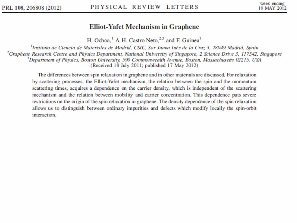
1) Understanding of spin relaxation in graphene (see Ochoa-Guinea,
PRL 2012) and lengthening of the spin diffusion length


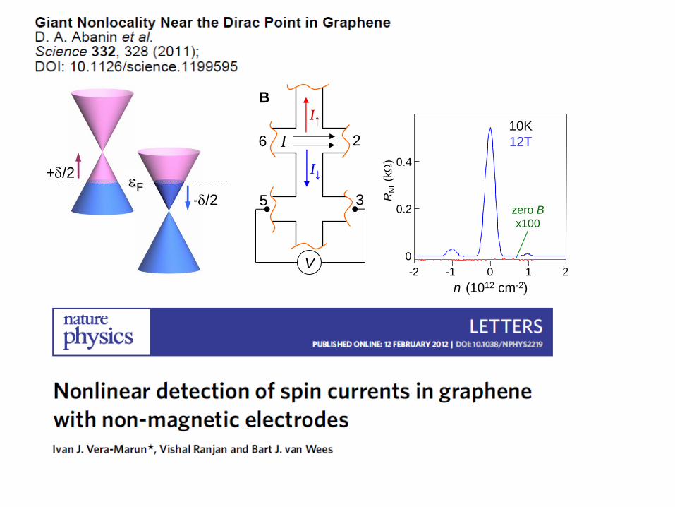
+/2
-/2
F
B
V
2
3
I↓
6
5
I
I↑
-2 -1 0 2 1
n (1012 cm-2)
RN
L (k
)
0
0.2
0.4
zero B
x100
10K
12T

Hill et al, IEEE-TM 2006, Tombros et al, Nature 2007, Cho et al, APL 2007,
Ohishi et al, Jap.J.Appl.Phys.2007, Nishioka et al, APL 2007, Goto et al, APL2008,
Jozsa et al, PR b 2009, Wang et al, PR B 2008, Han et al, PRL 2010, Yang et al, PRL
2011 and further publications from Groningen, Osaka, Riverside, Singapore, Aachen,
etc
Spin transport in graphene, examples of previous results
First experiments: spin diffusion lengths (< 1 m) and spin relaxation times were
found shorter than expected (from small S-O, weak hyperfine interactions)
but, today, begin to increase progressively
Example of recent results: van Wees et al (Groningen), private communication
graphene on BN: spin diffusion length 6 m
( longer than in metals or semiconductors
but still small compared to > 20 m for CNT)
graphene on Si-face SiC: spin relaxation time sf 2.35 ns ( 50 ns for CNT)
I
L
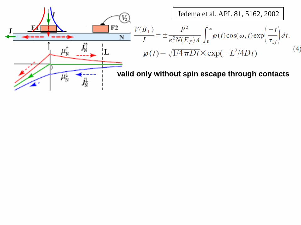
Jedema et al, APL 81, 5162, 2002
valid only without spin escape through contacts
I
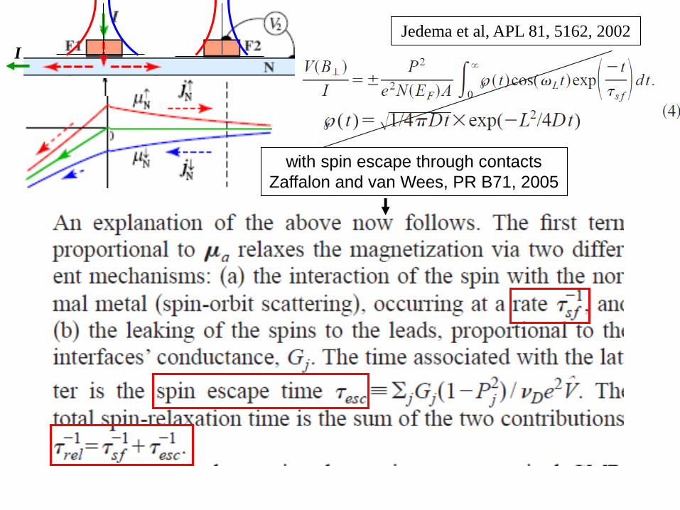
Jedema et al, APL 81, 5162, 2002
with spin escape through contacts
Zaffalon and van Wees, PR B71, 2005
I
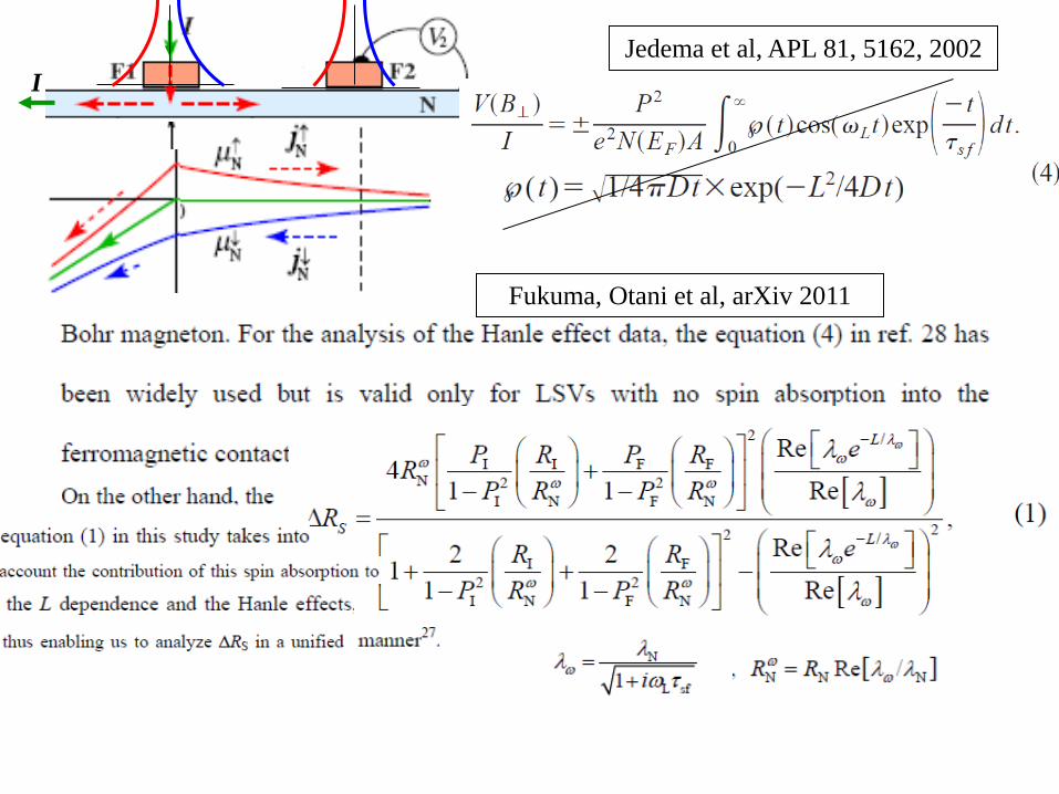
Jedema et al, APL 81, 5162, 2002
Fukuma, Otani et al, arXiv 2011
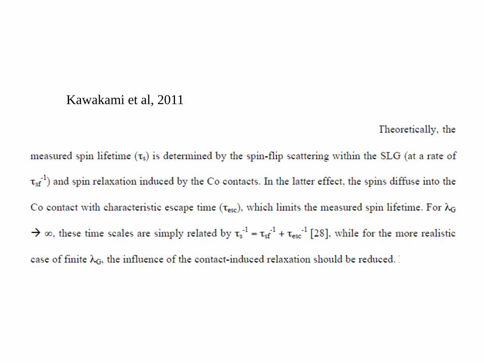
Kawakami et al, 2011
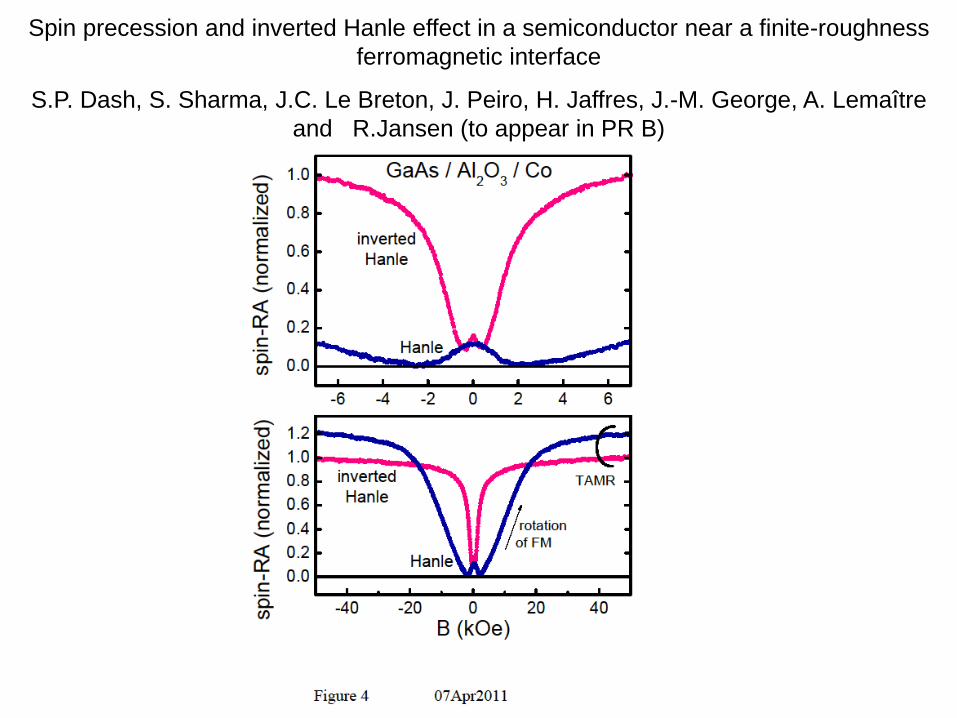
Spin precession and inverted Hanle effect in a semiconductor near a finite-roughness
ferromagnetic interface
S.P. Dash, S. Sharma, J.C. Le Breton, J. Peiro, H. Jaffres, J.-M. George, A. Lemaître
and R.Jansen (to appear in PR B)
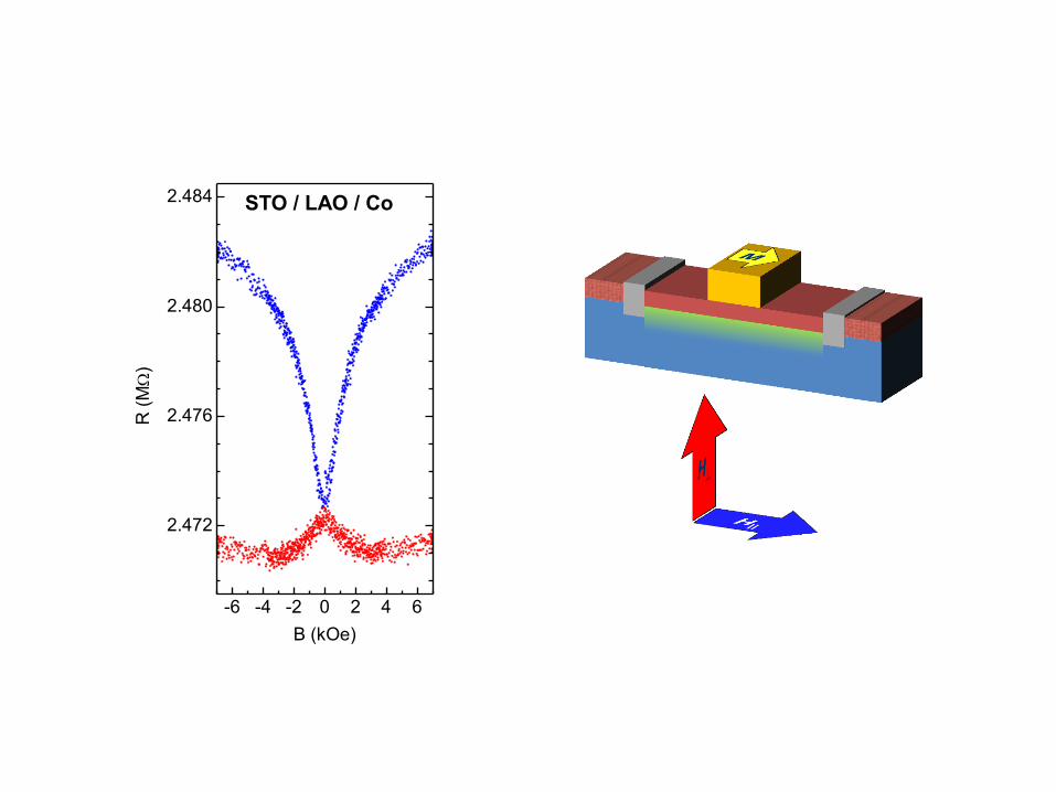
-6 -4 -2 0 2 4 6
2.472
2.476
2.480
2.484
R
(M
)
B (kOe)
STO / LAO / Co

Sprinkle et al, arXiv:1001.3869v1,2010
C-face
10 layers

Sprinkle et al, arXiv:1001.3869v1, 2010.
AB stacked bilayer
Single graphene sheet
(C-face)
C-face
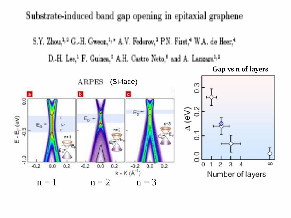
Gap vs n of layers
n = 1 n = 2 n = 3
(Si-face)

Al2O3
Co
Al2O3
Co
Graphene RTunnel LSMO LSMO
MW-CNT
L=1.5 m Tunnel RT Tunnel RT
RTunnel
Interpretation, determination of spin lifetimes and diffusion lengths
R/R +
window
L = λch/100
L = λch/2
Too long dwell time Too fast spin escape
Sch
RL
chTR
TRLdwell
*
for long too
*
wchchSch
R
Sch
RTR
/ressitance interface
ratio) resistance/spin resistance interface(/*
Sch
Rch
LTR
*