towards an all-opticalpseudo-random binary sequence...
TRANSCRIPT

Towards an all-optical pseudo-randombinary sequence generator
by Silvia Wagemans

iii
Eindhoven University of TechnologyFaculty of Electrical EngineeringDivision of Telecommunication Technology and ElectromagneticsElectro-Optical Communications Group
TTETowards an all-optical pseudo-random binary sequence generator
by Silvia Wagemans
Master of Science Thesiscarried out from June 2004 to August 2005
Supervisors:H.J.S. DorrenS. Zhang
Graduation professor:A.MJ. Koonen
The Faculty of Electrical Engineering of Eindhoven University of Technology disclaimsall responsibility for the contents of traineeship and graduation reports.

Summary
The graduation report presented gives a description of the development of an optical pseudo-random binary sequence (PRBS) generator, which is known to be oneof a few optical digital processing systems developed so far. It is described howthe known electric PRBS generators are builded up, from which the design of anoptical PRBS generator is retrieved.The total system of the optical PRBS generator consists of two optical flip-flopmemories ([1]) that combined with a clock signal form an optical shift-register([2]), and a XOR gate. The optical flip-flop memory used ([1]) has two different wavelengths at which it can operate. Therefore, the developed optical PRBSgenerator is not operating at the binary encoding principle, data encoded by twobinary intensity levels ON and OFF, but operates at the wavelength encoding principle, data encoded by two different wavelengths.One of the most important elements that needed to be developed for this systemwas the exclusive OR (XOR) gate. This XOR gate has to operate at low powerand produce a stable output. Further it is important that the output signal of theXOR gate is a wavelength encoded data signal as it is used as the input of one ofthe flip-flops.In this case three types of XOR gates are designed and tested; (1) a XOR gatebased on cross-polarization modulation in a SOA, (2) a XOR gate based on FWMin a SOA and (3) a XOR gate based on the use of three ring lasers. The last XORgate turned out to be the one that could fulfill the features necessary to be ableto be integrated in the total digital system of the PRBS generator. After optimizing the performance of the separate building blocks, the whole is connected andthe output is measured. The output shows good agreement with the theoreticallyexpected output.

Contents
1 Introduction 1
2 Pseudo-random binary sequence generator 52.1 Electronic PRBS generator . . . . 52.2 Optical PRBS generator principles 7
3 The optical XOR gate 113.1 XOR gate based on cross-polarization modulation in a SOA. 12
3.1.1 Operating principle . 133.1.2 Experimental results . . . . . . . . . . 143.1.3 Summary................ 17
3.2 XOR gate based on four-wave mixing in a SOA 183.2.1 FWM in a SOA . . . . . . . . 193.2.2 Setup and operating principle 193.2.3 Experimental results . . . . . 213.2.4 Summary........... 22
3.3 XOR gate based on three coupled lasers 223.3.1 Setup and operating principle 233.3.2 Experimental results 253.3.3 Summary 27
3.4 Discussion........ 27
4 The optical PRBS generator 294.1 Experimental setup and results . . . . . . . . . . 30
4.1.1 Experimental setup of the flip-flops . . . 304.1.2 Experimental setup of the clock generator 324.1.3 Experimental results for the optical shift-register 334.1.4 Experimental results of connecting the flip-flops to the
XOR gate. . . . . . . . . . . . . . . . . . 344.2 Experimental results on the optical PRBS generator 364.3 Summary . . . . . . . . . . . . . . . . . . . . . . 37

viii
5 Conclusions and recommendations
A Operation principle of the optical flip-flop memoryA.I The equations describing the flip-flop memory.A.2 Simulation results . . . . . . . . . . . . . . . . .
CONTENTS
41
474749

Chapter 1
Introduction
This report gives a description of the work I have done during my graduationproject at the Eindhoven University of Technology (TU/e) at the faculty of electrical engineering. This graduation project is the final part of the program in electrical engineering. During this graduation project I have carried out research in thearea of optical communication networks in the Electro-Optical Communications(ECO) group. The goal of the graduation project was to develop a pseudo-randombinary sequence (PRBS) generator for testing of high-speed optical components,making use of the optical flip-flop memory [1], which operating principle andsimulation results is described in Appendix A. In this chapter an introduction isgiven on the research done in the area of developing an optical PRBS generator.
Optical networks become more and more important and are already partly replacing the standard electrical networks. Total optical networks in the future is theoptimum goal. To achieve this goal it is necessary to develop optical componentsthat establish a high switching speed at low switching energies. It is expected thatall-optical signal processing systems are necessary in order to reach these highspeeds. In [1] the development of a small piece of an optical network, a flip-flopmemory is described, both experimentally as well as theoretically. With the helpfrom this optical flip-flop memory an optical shift-register has been realized, [2].This optical shift-register will form the base for the development of the pseudorandom binary sequence (PRBS) generator.
The general content of the report presented will describe the work done and theresults obtained during the graduation project; the design of an optical PRBS generator that makes use of the flip-flops described in [1]. In the literature so faronly a few cases are known where a total optical digital signal processing systemis developed. [3], [4]. Optical signal processing systems are becoming more ofinterest because of the increasing data rates of the optical networks, widely inte-

2 Introduction
grated nowadays, which electrical signal processing systems often cannot reach.By developing all-optical digital signal processing systems that can replace theirelectrical counterparts, the high data rates encountered with the optical networkscan be maintained. Important feature of the optical signal processing system is ahigh switching speed and a low switching energy. By developing an optical PRBSgenerator it will become possible in the future to measure the noise performanceof optical communication systems operating at high data rates, thereby verifyingthe integrity of optical transmission systems.
In chapter 2 the important features of electrical PRBS generators will be explainedand why it is necessary to develop an optical PRBS generator. It is explained whatthe design for an optical PRBS generator will be and how this is developed, making use of the optical flip-flop memory described in [1]. With two of these flip-flopmemories an optical shift-register can be made, [2]. Connecting the shift-registerwith an optical exclusive OR (XOR) gate resolves in a PRBS generator. As itturned out the hard part of developing this optical PRBS generator was the XORgate. The important features that the XOR gate needs to apply to if it used in thelarger system of the PRBS generator is that
1. it produces a stable output, as it is a part of larger system stability is veryimportant,
2. it can operate at low power injected, as it is known that the output power ofthe flip-flop memories used are low,
3. it operates at the wavelength encoding principle (data encoded in two different wavelengths) instead of at the binary encoded principle (data encodedby the binary intensity of the signals).
The last necessary feature is a result of the flip-flop memories used in the totalsetup, as they can operate at two different states, concerning two different wavelengths. The experimental stage of this graduation project was concentrated onthe development of a XOR gate that could fulfill these three features. In chapter 3an overview will be given of the XOR gates tested. Three different types of XORgates will be described, because the first two XOR gates tested could not fulfill thefeatures necessary to be implemented in the system of the PRBS generator. TheXOR gates tested are:
1. XOR gate based on cross-polarization modulation in a SOA,
2. XOR gate based on four-wave mixing (FWM) in a SOA,
3. XOR gate based on three coupled lasers.

3
The setup and operating principle of these XOR gates and the experimental resultsobtained with them is described and discussed. The reasons for not choosing thefirst two XOR gates as the ones used in the setup of the PRBS generator will begiven, as well as the reasons why the third XOR gate can be used in the totalsystem of the PRBS generator.In chapter 4 the optical PRBS generator will be described, as well as its buildingblocks. The issues concerning the setups of the building blocks are described.These building blocks are connected to each other step by step, thereby optimizingthe operating principle of the total PRBS generator step by step. Finally the totalPRBS generator has been tested. The results obtained with this total setup areshown and the power specifications are given.Finally in chapter 5 the conclusions of the research done and recommendationsfor further research in the area of optical PRBS generators are presented.

Chapter 2
Pseudo-random binary sequencegenerator
Pseudo-random binary sequence generators (PRBS generators) are commerciallyapplied in the area of electrical and electronic engineering. Their randomness isone of their most important properties, because they are very useful in producing (repeatable) white noise test patterns when measuring the noise performanceof communications, control and instrumentation systems. PRBS generators aremainly used for eye diagram, BER and jitter measurements.For the development of future optical fiber communication systems and their highspeed components often PRBS generators are used. For this purpose reliabletesting is required at multi-GHz frequencies. The availability of this PRBS testequipment is frequently a limiting factor, because commercially available electronic PRBS test equipment cover data rates up to 15 Gbits/s, [5]. It is thereforeimportant to develop optical PRBS generators than can cover larger data rates thanthese electronic PRBS generators.In this chapter the principle and design of an optical PRBS generator will be described. At first a glance will be taken on electronic PRBS generators. From thisprinciple an optical PRBS generator is developed. This optical generator has tomake use of the optical flip-flop memory described in [1].
2.1 Electronic PRBS generator
Maximal-length shift register sequences, or m-sequences are known as good electronic PRBS generators. To construct an m-sequence of length N = 2m - 1, oneneeds as a basis a primitive polynomial c(x) of degree m, for instance:

6 Pseudo-random binary sequence generator
( ) m + m-I + m-2 + + + ""m iC X = CmX Cm-IX Cm -2X . . . CIX Co = Li=O Ci X ,
where Co = Cm = 1. This polynomial specifies a linear feedback shift register(LFSR), as presented in figure 2.1.
F Foutput
Figure 2.1: Linear feedback shift register (LFSR) corresponding to c(x). F represents the memory element, CI to CN-I represent the feedback equal to 0 or 1 andE9 represents a XOR gate
This LFSR consists of m boxes, representing memory elements or flip-flops, eachcontaining a binary 0 or 1. At each clock pulse the contents of the boxes areshifted one place to the right. The boxes corresponding to the terms in c(x) areadded and fed back to the left-hand box. The sum is calculated modulo 2, so E9in the figure represents a modulo-2 adder or exclusive OR (XOR) gate, defined bythe truth table 2.1:
Ini In2 Out0 0 00 1 11 0 1I 1 0
Table 2.1: Truth table for the XOR gate.
From this it follows that from a given polynomial, a sequence can be generatedby an m-stage binary LFSR which has a feedback tap connected to the output ofthe ith box if Ci = I and no feedback tap if Ci = O. Such an m-stage binary LFSRrepresents an electronic PRBS generator. These PRBS generators are known tohave a certain period after which the same random signal is repeated, thereforethey are called pseudo-random. The length of the period depends on the amountof memory elements used and can be calculated in as follows: period = 2m - I

2.2 Optical PRBS generator principles 7
(an example: if m is 3, the period is equal to 8 bits, meaning that after 8 bitsthe signal will repeat itself). To start up the shift register, the initial values of thememory elements should be specified. If all the memory elements are equal to 0,the output of the PRBS generator will stay 0 as well, so care must be taken thatthis is not the case.All known electronic PRBS generators are developed from the principle of theLFSR presented here. The period and thereby the randomness of the output signalcan be varied by changing the amount of memory elements used.
2.2 Optical PRBS generator principles
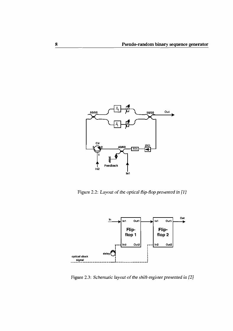
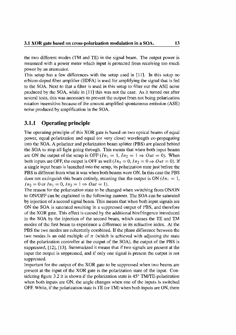
The design of an all-optical PRBS generator can be extracted from the generalprinciple of the electrical PRBS generator. The necessary elements are an opticalshift-register build out of optical memory elements and an optical XOR gate. Themost important condition for the design is that the optical memory element used,is the optical flip-flop memory described in [1].The flip-flop memory ([1]) consist of two coupled ring lasers, made bi-stable bythe presence of a feedback, see figure 2.2. The flip-flop has two inputs and twooutputs. In each stable state one of the lasers lases while the other one is suppressed, making the state of the flip-flop memory dependent of the wavelength ofthe dominant laser. The operating principle and some simulations results gainedwith the equations describing this optical flip-flop memory is described in Appendix A.In [2] an optical shift-register is made with two of these flip-flop memories coupled driven by common clock pulses. The schematic configuration is presentedin figure 2.3. The two cascaded flip-flops are driven by an optical clock pulse tobe able to clear the state of the optical flip-flops. A strong clock signal saturatesthe SOA of the flip-flops after which its state can be set by the signal present atIn] of the input. The power of the external optical clock signal is divided into twoparts. On part is delayed, while the other part is used to clear the state of flip-flop2, by injection via port In2. The output from flip-flop 1 then sets the new state offlip-flop 2. If flip-flop 2 is set to its new state the delayed clock signal is injectedinto port In2 of flip-flop 1 to clear its state subsequently. The signal present atport In] of the flip-flop 1 then sets the new state of this flip-flop. This optical shiftregister forms the base of the optical PRBS-generator.The schematic configuration of the simplest optical PRBS generator possible isshown in figure 2.4. It makes use of two optical flip-flop memories, that combined with a clock signal form an optical shift register and an optical XOR gateThe optical PRBS generator operates in the following fashion. Flip-flop 1 of theshift register is set to its new state after being cleared by the clock signal by the
8 Pseudo-random binary sequence generator
In2
In1
Out
optical clock
Figure 2.2: Layout of the optical flip-flop presented in [1]
In OutIn1 oun In1 oun
Flip- Flip-flop 1 flop 2
,.-- In2 Out2 r-- In2 Out2I II
delay0I___~~~n!! : ~
Figure 2.3: Schematic layout of the shift-register presented in [2]

2.2 Optical PRBS generator principles
In1 Out1
flip-flop
.Clock : L.-_---'input :-------------------------
In1 Out1
flip-flop
PRSSoutput
9
Figure 2.4: General principle of the optical PRBS generator
signal at the output of the XOR gate. The XOR gate is set to a new state by theoutput signals of flip-flop I and flip-flop 2 of the shift register. This means that theXOR gate that has to be used in this setup has to operate at the wavelength encodedprinciple, the principle that optical data is encoded by two different wavelengths.In this case these two different wavelengths have to correspond to two states ofthe optical flip-flop memory used. If it is determined that A1 represents a binary"0" and A2 represents a binary" 1"', the truth table for the XOR gate will be:
Inl In2 Out
Al Al AlAl A2 A2A2 Al A2A2 A2 Al
Table 2.2: Truth table for the wavelength encoding XOR.
The output of the optical PRBS generator shown in figure 2.4 has a length of 3bits (N = 2m - 1), meaning that after 3 bits the output signal repeats itself. Ifthe initial value of the flip-flops is equal to A2 (binary" 1") for both flip-flop 1 andflip-flop 2, the output of the PRBS generator will show a repeating AIA2A2 (binary"all ") at its output. Care has to be taken that the initial states of the flip-flops isnever A1 for both of them at the same time, cause then a never ending sequence ofA1 will be produced by the PRBS generator.The difficulty for the design of this PRBS generator is to develop an optical XORgate that can be used in this experiment. Firstly, the XOR gate has to operate at thewavelength encoded principle. Secondly, the XOR gate that needs to be developedis a stable XOR gate. As it is a part of a larger optical digital signal processing

10 Pseudo-random binary sequence generator
system this is necessary. The XOR gate needs to set the state of flip-flop 1 afterthis is cleared, so if the output would not be stable, this could cause flip-flop 1to be set to the wrong value, which causes the PRBS generator to work wrong.Thirdly, the XOR gate has to operate at low input powers injected as it is knownthat the output power of the flip-flops is equal to -3.5 dBm or even lower. Nextto the low output powers of the flip-flops, the output signals are not continuouswave (CW) signals, but look like the signal shown in figure 2.5.. This means that
Figure 2.5: A representation ofa binary 1 coming from the optical flip-flop memory.
the average power of the output of the flip-flop memory is equal to -3.5 dBm. Sothe power of the signal at the input of the XOR gate canbe even much lower than-3.5 dBm, which means that the XOR gate has to operate at these lower powersinvolved as well. The development of such an XOR gate that can fulfill these threeimportant features mentioned above will be described in the next chapter.

Chapter 3
The optical XOR gate
A XOR gate that can be used in the all-optical digital signal processing systemof the PRES generator was the most difficult part of the experimental side of theproject. The most important features the XOR gate had to fulfill were being ableto operate at low powers involved, produce a stable output and be able to workwith data encoded by two different wavelengths. The most optical XOR gatesknown from the literature, [6], [7], [8], [9] and [10], cannot be used as they workon the binary encoding principle.In total three types of XOR gates have been investigated and tested in search forthe one that could fulfill. all the necessary features for being implemented in thesystem of the optical PRES generator. These three types of XOR gates are:
1. XOR gate based on cross-polarization modulation in a SOA,
2. XOR gate based on four-wave mixing in a SOA,
3. XOR gate based on three coupled lasers.
In this chapter the setup and operating principle of the three types of XOR gatesthat possibly can be used in the system of the optical PRES generator will described. With all three of them measurements are done to find out if it is possiblefor the specific XOR gate to fulfill the desired features. The results of these measurements are presented. From the outcome the decision is made whether thisXOR gate will be useful for implementation in the total setup of the PRES generator. As it turns out the third setup is the only one that can fulfill the desiredfeatures.

12 The optical XOR gate
3.1 XOR gate based on cross-polarization modulation in a SOA.
For developing a XOR gate that can fulfill the desired features, the following approach is taken:
Inl In2 Outcase 1 Al Al Al
Al A2 A2A2 Al A2
case 2 A2 A2 Al
The last case forms the exception, and only when this case can be fulfilled as wella XOR gate is developed.Keeping this approach in mind the XOR gate that makes use of the cross-polarizationmodulation effect in a semiconductor optical amplifier (SOA) [11] is tested. Itssetup is presented in figure 3.1.
Powermeter
11 11 1
Output 1MLaser1
Laser2
Figure 3.1: The experimental setup of the XOR
It consists of two lasers, three polarization controllers (PCs), a coupler, two isolators, a SOA, a filter and a polarization beam splitter (PBS). The two lasers emita continuous wave (CW) probe beam at wavelength A2. These beams are polarization controlled to adjust the polarization state of the input signals with theorientation of the SOA layers. They are coupled together and fed through an isolator to the SOA. The output of the SOA is polarization controlled to adjust thepolarization of the amplified signal with the orientation of the PBS. The filter isused make sure that the amplified spontaneous emission (ASE) of the SOA doesnot influence the polarization state of the signal before entering the PBS. The output of the filter serves as an input for the PBS. This PBS is used to distinguish
3.1 XOR gate based on cross-polarization modulation in a SOA. 13
the two different modes (TM and TE) in the signal beam. The output power ismeasured with a power meter which input is protected from receiving too muchpower by an attenuator.This setup has a few differences with the setup used in [11]. In this setup noerbium-doped fiber amplifier (EDFA) is used for amplifying the signal that is fedto the SOA. Next to that a filter is used in this setup to filter out the ASE noiseproduced by the SOA, while in [11] this was not the case. As it turned out afterseveral tests, this was necessary to prevent the output from not being polarizationrotation insensitive because of the amount amplified spontaneous emission (ASE)noise produced by amplification in the SOA.
3.1.1 Operating principle
The operating principle of this XOR gate is based on two optical beams of equalpower, equal polarization and equal (or very close) wavelength co-propagatinginto the SOA. A polarizer and polarization beam splitter (PBS) are placed behindthe SOA to stop all light going through. This means that when both input beamsare ON the output of the setup is OFF (Inl = 1, In2 = 1 :::} Out = 0). Whenboth inputs are OFF, the output is OFF as well (Inl = 0, In2 = 0 => Out = 0). Ifa single input beam is launched into the setup, its polarization state just before thePBS is different from what it was when both beams were ON. In this case the PBSdoes not extinguish this beam entirely, meaning that the output is ON (Inl = 1,In2 = Oor In! = 0, In2 = 1 => Out = 1).The reason for the polarization state to be changed when switching from ON/ONto ON/OFF can be explained in the following manner. The SOA can be saturatedby injection of a second signal beam. This means that when both input signals areON the SOA is saturated resulting in a suppressed output of PBS, and thereforeof the XOR gate. This effect is caused by the additional birefringence introducedin the SOA by the injection of the second beam, which causes the TE and TMmodes of the first beam to experience a difference in its refractive index. At thePBS the two modes are coherently combined. If the phase difference between thetwo modes is an odd multiple of Jr (which is achieved with adjusting the stateof the polarization controller at the output of the SOA), the output of the PBS issuppressed, [12], [13]. Summarized it means that if two signals are present at theinput the output is suppressed, and if only one signal is present the output is notsuppressed.Important for the output of the XOR gate to be suppressed when two beams arepresent at the input of the XOR gate is the polarization state of the input. Considering figure 3.2 it is shown if the polarization state is 45° TMITE-polarizationwhen both inputs are ON, the angle changes when one of the inputs is switchedOFF. While, if the polarization state is TE (or TM) when both inputs are ON, there

14 The optical XOR gate
is no change in the angle when one of the inputs is switched OFF. Therefore it isexpected that if the inputs are 45° TEffM-polarized, the difference between thesuppressed and not suppressed output is the highest. After testing the setup shown
Asin8
TE
AcosS
AON/ON
ON/OFF
Figure 3.2: Polarization states.
in figure 3.1 with 45° TMffE-polarized inputs and TE-polarized inputs it turns outthat the difference between the suppressed and not suppressed output of the XORgate is the highest when the polarization state of the inputs is TE-polarization.
3.1.2 Experimental results
The performance of the XOR is tested by measuring the contrast ratio. The contrast ratio is equal to the difference in the suppressed and not suppressed outputof the XOR gate. The contrast ratio needs to be at least 10 dB for the XOR gateto be applicable in the system of the optical PRBS generator. The contrast ratiois strongly dependent from current of the SOA and the power level of the inputs.The higher the SOA current, the higher the polarization rotation in the SOA is,which results in a high contrast ratio. Next to that, a higher input powers resultsin a higher contrast ratio. Therefore the contrast ratio is measured for differentcurrents of the SOA and for different input powers injected. The setup for thesemeasurements is equal to the setup shown in figure 3.1.The powers injected are made equal for both inputs, as would be more or less thecase if the signals would be coming form the flip-flops. The measurements aredivided into two sections:
1. for high power operation,
2. for low power operation

3.1 XOR gate based on cross-polarization modulation in a SOA. 15
For one value of the injected power at a certain value of the SOA current, severalcontrast ratios are measured. From these, the mean is taken, to be sure that thecontrast ratio measured is as accurate as possible.
Contrast ratio for high powers operation
The power injected is varied from -0.8 dBm till 2.2 dBm. The SOA current isvaried from 200 rnA till 395 rnA (the maximal current that the SOA can handleis 400 rnA), in diverting steps. As it turned out the performance of the XOR gatewas rather poor at 200 rnA, and therefore the current was enlarged with 50 rnA,while as the performance got much better at 350 rnA it was enlarged with 5 rnA.Eventually, the best performance of the XOR gate was measured at a current of395 rnA. The results at this current turned out to be the most stable one and thecontrast ratio is the highest at a current of 395 rnA, and therefore the results forthis current are presented. The measured contrast ratio is equal to the differencein when both inputs are ON and when one of the inputs is ON (suppressed and notsuppressed).In figure 3.3 the mean measured contrast ratio is plotted against the injected power.
Contrast ratio at 395mA
14,---- ---,
iD:!i!-
to1iia:oc:E
2.51.50.5
P_inj (dBm)
-0.5
2 •••••••••••••••••••••••••••••••••••••••••••••••••••••••••••••••••••••••••••••• -+-CR_ In1, OFF.
__ CR_IN2, OFFo.l----,---,....----,---,....--..:;::==::::::;;:::===~
-1
Figure 3.3: Mean contrast ratio at 395 rnA for high input powers. CR_In 1, 0 F Fshows the measured mean contrast ratio between both inputs on and input 1switched off, and CR_In2, 0 F F shows the measured mean contrast ratio between both inputs on and input 2 switched off.

16 The optical XOR gate
The fluctuations seen in this figure are caused by the fact that the contrast ratioat the output of the setup is not staying stable. Before every measurement thepolarization state of the inputs is set to right polarization state (TE-polarization),because it is known that form a system made out of fiber pigtailed components intime the polarization states change due to temperature changes and environmentalchanges. This results in a different contrast ratio for the same input power, whichresults in the fluctuations in the mean contrast ratio visible in figure 3.3.
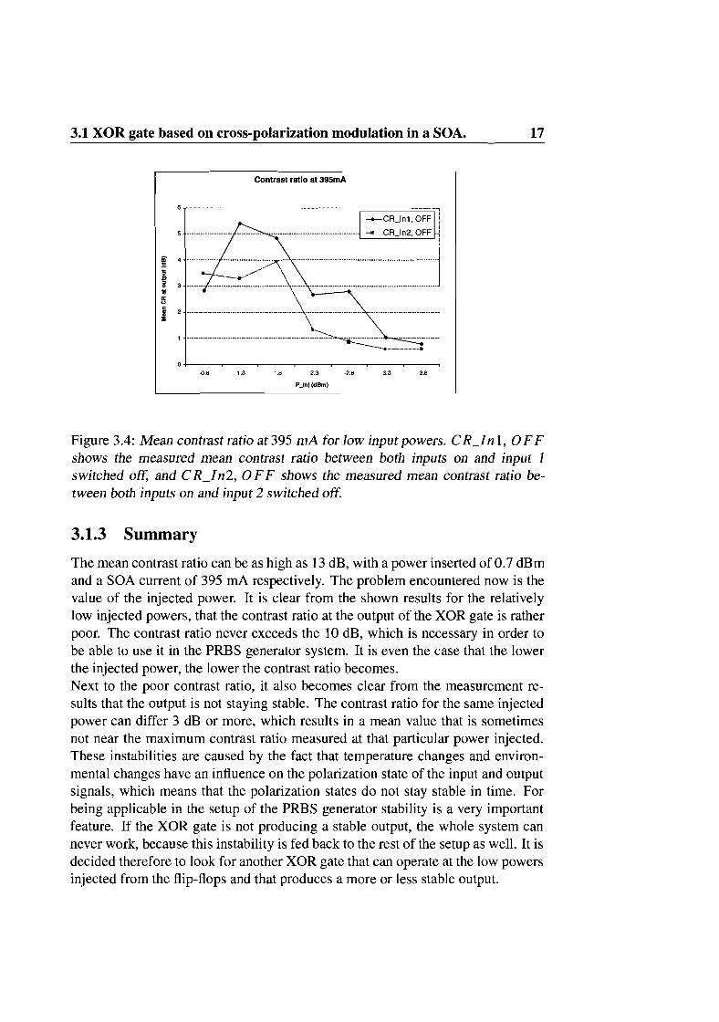
Contrast ratio for low powers operation
It is has been shown that this XOR gate can work at relatively high powers injected (although it is not really stable), but it is necessary to know how the overallperformance is if relatively low powers are injected (as one of the important features of the XOR gate is that it has to operate at low powers involved to be ableto be used in the system of the optical PRBS generator). So far the lowest powerinjected was -0.8 dBm, and it is already clear from figure 3.3, that at this powerthe output is not performing at best. To get a clear overview how this XOR gateis exactly behaving at low powers, more measurements have been done at lowinjected powers.The injected power is varied from -0.8 dBm till -3.8 dBm, in steps of 0.5 dBm.The mean contrast ratio for each injected power is calculated and plotted in figure3.4. The contrast ratio is equal to the difference in when both inputs are ON andwhen one of the inputs is ON.The fluctuations seen in this figure are also caused by the fact that the contrast ratioat the output of the setup is not staying stable, as was the case with the measuredmean contrast ratio in figure 3.3. Before every measurement the polarization stateof the inputs is set to the right polarization state (TE-polarization), because it isknown that from a system made out of fiber pigtailed components in time the polarization states change due to temperature changes and environmental changes.This results in a different measured contrast ratio for the same input power, whichresults in the fluctuations in the mean contrast ratio visible in figure 3.3.
3.1 XOR gate based on cross-polarization modulation in a SOA. 17
Contrast ratio at 395mA
-3.8-3.3-2.8-1.8
-+-CR_lnl, OFF
........................................ --CR_ln2, OFF
-1.3-0.8
Figure 3.4: Mean contrast ratio at 395 rnA for low input powers. C R_In 1, 0 F Fshows the measured mean contrast ratio between both inputs on and input 1switched off, and C R_In2, 0 F F shows the measured mean contrast ratio between both inputs on and input 2 switched off.
3.1.3 Summary
The mean contrast ratio can be as high as 13 dB, with a power inserted of 0.7 dBmand a SOA current of 395 rnA respectively. The problem encountered now is thevalue of the injected power. It is clear from the shown results for the relativelylow injected powers, that the contrast ratio at the output of the XOR gate is ratherpoor. The contrast ratio never exceeds the 10 dB, which is necessary in order tobe able to use it in the PRBS generator system. It is even the case that the lowerthe injected power, the lower the contrast ratio becomes.Next to the poor contrast ratio, it also becomes clear from the measurement results that the output is not staying stable. The contrast ratio for the same injectedpower can differ 3 dB or more, which results in a mean value that is sometimesnot near the maximum contrast ratio measured at that particular power injected.These instabilities are caused by the fact that temperature changes and environmental changes have an influence on the polarization state of the input and outputsignals, which means that the polarization states do not stay stable in time. Forbeing applicable in the setup of the PRBS generator stability is a very importantfeature. If the XOR gate is not producing a stable output, the whole system cannever work, because this instability is fed back to the rest of the setup as well. It isdecided therefore to look for another XOR gate that can operate at the low powersinjected from the flip-flops and that produces a more or less stable output.

18 The optical XOR gate
3.2 XOR gate based on four-wave mixing in a SOA
It is known that the powers coming from the flip-flops are very low (around -3.5dBm or even lower). Therefore there has to be thought of another XOR gate thatis able to work at low input powers involved and which performance is also stable.The stability was the main problem of the previous described XOR gate.There is chosen for a change in approach when developing this new gate. Former the operating principle was divided in the following two cases: The last case
Inl In2 Outcase J Al Al Al
AI 1.2 1.21.2 AI 1.2
case 2 1.2 1.2 Al
formed the exception, and only if this condition also could be met the XOR gatewould be useful.Now the operating principle is divided in the following two cases: There is no
Inl In2 Outcase J Al 1.2 1.2
1.2 Al 1.2
case 2 Al Al Al1.2 1.2 Al
exception that needs to be fulfilled, but is is divided into the case where the twoinputs have the same wavelength and the case that the two inputs have differentwavelengths.Following this new approach developing an XOR gate based on the presence offour-wave mixing (FWM) in a SOA ( [15], [16], [17], [18]" [19], [20], [21] ), islaunched. This FWM in a SOA has already been used to develop optical logicgates, as can be read in [23] and [22]. Problems that will be encountered withthis XOR gate is that the feature of operating at low input powers will be hard toachieve.In this chapter the operating principle and experimental setup of this XOR gatewill be described after it is explained what FWM in a SOA is and how this haslead to the design of a XOR gate.

3.2 XOR gate based on four-wave mixing in a SOA
3.2.1 FWM in a SOA
19
Four-wave mixing in a SOA is a nonlinear process that can occur between twooptical fields entering a SOA. These two signals, having different wavelengths O"sand At) modulate the amplifier gain. Nonlinear gain saturation gives rise to newoptical fields at wavelengths of AFWMj = 2As - At and AFWM2 = 2At - As withfrequencies respectively of W FWMj = 2ws - Wt and W FW M2 = 2wt - Ws' In figure3.5 an example of such an amplifier output spectrum is drawn. It shows an idealsituation, where the power of the two formed FWM-signals is equal. Mostly thepower of the first formed FWM-component is relatively higher than the secondone.
-10
-20
-30
1552 1553 1554 1555 1556
Wavelength (nm)
Figure 3.5: Example of a spectrum with FWM at the output ofa SOA.
3.2.2 Setup and operating principle
The total setup for this XOR gate is presented in figure 3.6.The operating principle of this XOR gate can be described as following. If two
wavelength identical signals (A] and A] or A2 and A2) enter the the SOA, no FWMsignals will be visible at the output of this SOA, because if the wavelengths, andtherefore the frequencies are identical, no gain modulation of the SOA occurs.If two wavelength different signals (A] and A2) enter the SOA, the two FWMsignals will be visible at the output of the SOA. The wavelengths of these twoFWM-signals is equal to 2A] - A2 and 2A2 - A]. The power of the signal at a
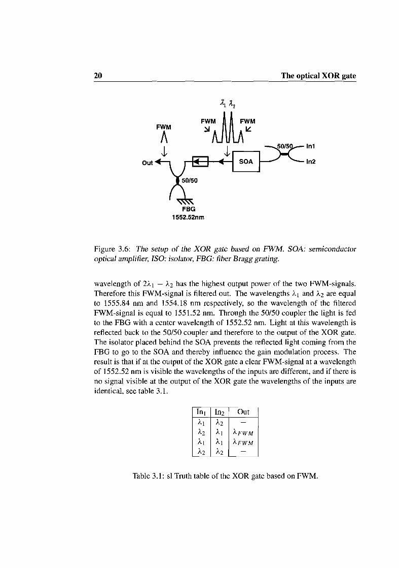
20
Out
~~
FWM ~ ~ FWM
~A1VLA~J,.-----.........
SOA
FBG1552.52nm
The optical XOR gate
In1
In2
Figure 3.6: The setup of the XOR gate based on FWM. SOA: semiconductoroptical amplifier, ISO: isolator, FBG: fiber Bragg grating.
wavelength of 2Al - A2 has the highest output power of the two FWM-signals.Therefore this FWM-signal is filtered out. The wavelengths Al and A2 are equalto 1555.84 nm and 1554.18 nm respectively, so the wavelength of the filteredFWM-signal is equal to 1551.52 nm. Through the 50/50 coupler the light is fedto the FBG with a center wavelength of 1552.52 nm. Light at this wavelength isreflected back to the 50/50 coupler and therefore to the output of the XOR gate.The isolator placed behind the SOA prevents the reflected light coming from theFBG to go to the SOA and thereby influence the gain modulation process. Theresult is that if at the output of the XOR gate a clear FWM-signal at a wavelengthof 1552.52 nm is visible the wavelengths of the inputs are different, and if there isno signal visible at the output of the XOR gate the wavelengths of the inputs areidentical, see table 3.1.
Inl In2 OutAl A2 -
A2 )1.1 AFWM
Al Al AFWM
A2 A2 -
Table 3.1: sl Truth table of the XOR gate based on FWM.

3.2 XOR gate based on four-wave mixing in a SOA
3.2.3 Experimental results
21
At a wavelength spacing of 1.6 nm between the two wavelengths Al and A2 thecontrast ratio is measured at different values of the input powers. The contrastratio is equal to the difference in power when AFW M is present and when it isnot present at the output of the XOR gate. The signals used are CW-signals. Theresults ofthis measurement is shown in figure 3.7.
Contrast ratio at different powers injected
20
18
E 16ED~ 14o!
12
!g 10o
6 ••••
4-l--=------.-------,,----....---------r-=====:;:==...J-4 -2
P_inj (dBm)
Figure 3.7: Results of measuring the contrast ratio at the output of the XOR gateat different powers injected. CR_l, off represents the contrast ratio between aFWM-signal visible at the output of the XOR gate and no FWM-signal present atthe output due to the switching off of input 1. C R_2, off represents the contrastratio between a FWM-signal visible at the output of the XOR gate and no FWMsignal present at the output due to the switching off of input 2.
From figure 3.7 it can be seen that the higher the input power the higher the contrast ratio is. The most important conclusion from this measurement done is thatthe contrast ratio is highly dependent of the input powers. The contrast ratio needsto be 4 dB to be able to use this XOR gate in the system of the optical PRBS generator. Therefore every effort must be taken to make the powers at the XOR gateinputs as high as possible to be able to have a high as possible contrast ratio.The contrast ratio is measured when signals equal to the signals coming from theflip-flops are injected into the XOR gate. As it turns out the contrast ratio between a FWM-signal present and no FWM-signal present is 0 dB, meaning thatthe powers of the input signals is too low, to achieve FWM in the SOA. Therefore

22 The optical XOR gate
a SOA is placed before both inputs of the XOR gate, to make the power of theinputs higher. Then a contrast ratio of 0.15 dB can be measured. This low valueof the contrast ratio can be explained by considering the amplified spontaneousemission (ASE) noise that is present at the output of the SOA, which is, as it turnsout, almost as large in power as the FWM signal is.
3.2.4 Summary
From the results presented in this paragraph it has become clear that a XOR gatebased on FWM in a SOA can be developed and is a stable operating logic gate.The problem with this kind of gate is the power that is injected into it. This needsto be higher than the power at the output of the flip-flops in order to establishFWM in a SOA that is stronger then the noise produced by it. Amplifying theinput signals with two SOAs did not bring the required solution. The powers stillremained too low to observe a clear FWM in the SOA.
It can be concluded that this XOR gate cannot be used in developing a PRBSsystem, although it is stable operating logic gate, because it cannot operate at thelow powers involved. If it was necessary to develop a stable XOR gate that doesnot need to be integrated in a larger system, this design could be considered as anoption, seen its stable operation if the injected powers are high enough.
3.3 XOR gate based on three coupled lasers
In this section, an XOR gate that consists of three coupled lasers is considered.The most important feature that could not be met with the other two XOR gatesis a good operation at low input powers. The approach still stays the same, aswhen developing the XOR gate based on FWM in a SOA; The operating principle
In] In2 Outcase 1 A] A2 A2
A2 A] A2case 2 A] A] A]
A2 A2 A]
is divided into the case that both inputs have the same wavelength and that bothinputs have a different wavelength.It is known that coupled laser configurations are able to operate at relatively lowpowers involved and that lasing can be suppressed by injecting external light into

3.3 XOR gate based on three coupled lasers 23
it. The setup of a ring laser is shown in figure 3.8. The ring laser is not made
(a) (b)
In- In Out-
Ringlaser 1
A
Out
Figure 3.8: (a) The ring laser configuration. (b) The icon of the ring laser. Cir:circulator, ISO: Isolator, FBG: fiber Bragg grating.
out of a filter with a central wavelength of A, but out of a 50/50 coupler and FBGwith a central wavelength of A, because of the limited number of filters available.The operating principle is the same as with a filter involved; the FBG reflects thelight at the center wavelength A, into the right side of the SOA through the 50/50coupler and the isolator. The circulator prevents the reflected light going into theSOA from the left side, cause it acts as an isolator from port 3 to 2. At the outputof the ring laser a signal at a wavelength of A is present. If there is a signal presentat the input of the ring laser, this light is fed to the SOA, thereby saturating theSOA. When the SOA is saturated lasing is suppressed and no light is visible at theoutput of the ring laser.Keeping in mind that lasing of a ring laser can be suppressed by injecting externallight a XOR gate can be developed which makes use of three coupled lasers. Inthe next subparagraphs the setup and operating principle will be explained, as wellas the experimental results obtained with this XOR gate.
3.3.1 Setup and operating principle
The setup of the XOR gate was made out of three ring lasers as presented in figure3.9.
The operating principle can be explained with the help from figure 3.8, and is
24
IN1
IN2
Out
Ringlaser 1
~
Out
Ringlaser2
~
The optical XOR gate
Ringlaser3
~
OUT
Figure 3.9: The setup of the XOR gate made out of coupled lasers. Ring laser 1and 2 are lasing at wavelength )"1, ring laser 3 is lasing at wavelength A2. ISO:isolator.
mainly based on saturating the SOAs of the ring lasers thereby suppressing thelasing of them. The input signals are coupled together by a 50/50 coupler afterwhich the combined signals are filtered by a filter at wavelength AI that is connected to ring laser 1 and a filter at wavelength A2 that is connected to ring laser2. Ring laser 1 and 2 are both lasing at wavelength AI. If there is a signal comingfrom the filter with a center wavelength of AI, so if Al is injected into the XORgate, the SOA of ring laser 1 will be saturated by it. This prevents this laser fromlasing further. If there is a signal coming from the filter with a center wavelengthof A2, so if A2 is injected into the XOR gate, the SOA of ring laser 2 will be saturated by this light. This prevents this ring laser from lasing further. The outputsof ring laser 1 and 2 are coupled together and connected to ring laser 3, whichis lasing at wavelength A2. If there is a signal present at the input of ring laser 3its SOA is saturated, thereby suppressing lasing of this laser. If there is no signalpresent at the input of ring laser 3 this laser is lasing. The output of ring laser 3 iscoupled together with the light coming from ring laser 1 and ring laser 2, and thisforms the output of the XOR gate.If both Al and A2 are injected into the XOR gate, lasing of both ring laser 1 and2 is suppressed, resulting in a signal of wavelength A2 at the output of the XORgate, because ring laser 3 is lasing. If only A1 is injected into the XOR gate, ringlaser 1 is lasing, thereby suppressing lasing of ring laser 3. This results in signal atwavelength Al at the output of the XOR gate. If only A2 is injected into the XOR

3.3 XOR gate based on three coupled lasers 25
gate, ring laser 2 is lasing, thereby suppressing lasing of ring laser 3. This resultsin signal at wavelength A1 at the output of the XOR gate.In this way wavelength encoding XOR logic operation is obtained, keeping inmind what the truth table for a wavelength encoding XOR gate is, as shown intable 2.2.
3.3.2 Experimental results
For the SOAs of the first two ring lasers it is important that they produce a strongenough output signal to saturate the SOA of the third ring laser when lasing, butthat it is also possible to saturate them by the signals coming from filters. For theSOA of ring laser 3 it is important that it can be saturated by a signal coming fromring laser 1 or ring laser 2. Therefore it is important that the currents of the SOAsof the ring lasers are set to the right value. The higher the current of the SOA,the higher the output power of the ring laser will be, but the lower the current ofthe SOA the easier the SOA can be saturated and thus prevent the ring laser fromlasing. A compromise has to be found between these two situation when settingthe currents to the right values.It is possible to retrieve a nice XOR logic operation from the setup shown in figure3.9. The currents that drive the SOAs are set to 150.6 rnA, 149.8 rnA and 159.04rnA for the SOA of ring laser 1, the SOA of ring laser 2 and the SOA of ring laser3 respectively. The wavelengths A1 and A2 are equal to 1552.52 nm and 1558.91nm respectively. At the output of the XOR gate the spectrum is measured withan optical spectrum analyzer. The results of measuring the output spectrum areshown in figure 3.10.
The spectrum shows that if the signals injected into the XOR are different ofwavelength, which is equal to A1A2, the output is equal to A2. When the signalsinjected are equal of wavelength, which is equal to A1A1 or A2A2 , the output isequal to A1. This means that at output is correct for al the four situations possibleas presented in the truth table 2.2. The contrast ratio between the lasing wavelength and the suppressed wavelength is equal to 30 dB or more.The results shown are measured with signals inserted that are comparable to theones coming from the flip-flops in shape and power. This means that output spectrum shown in figure 3.10 is measured with signals inserted at a power of -3.5dBm and a shape equal to the one as shown in figure 2.5. (Of course the XORgate was first tested with CW signals injected into the XOR gate, but as it can bedone with signals that are equal to the signals coming from the flip-flops the resultof this measurement is shown.)

-20 ". i '
26
-10F~===::::r::====;r---~~-'l
II F-F1 =wavelength 1 I-20 H F-F2=wavelength 2 1-,,-
-30
-40
The optical XOR gate
-10 I--,----~~------;:========c::;"']
IF-F1=wavelength 1 I
" F-F2=wavelength 1
-30
-40
-60~~--~--~--~-~----'
-50 "---.r\.~ -,--__.....-- ',,-- -50~ \.--_-,---_........,.---J~
-60~~--~--~--~-~----'
1552 1554 1556 1558 1560 1552 1554 1556 1558 1560
-20
-10 ir=='==========:;r-------:--'11 F-F1 =wavelength 2 1
-20 -I F-F2=wavelength 1 I: ' ,
-30
-40
-50 '-.J\'-------'--_----:-_______ ''i.-....
-101--,----------,----;::r=====~
[F1=wavelength 2/' _" , '" F-F2=wavelength 2
/-30
-40
-50 \. (\ ,i-----'" ---_--1) L-
-60~~--~--~--~-~----J _60L_~--~--~--~-~----J
1552 1554 1556 1558Wavelength (nm)
1560 1552 1554 1556 1558Wavelength (nm)
1560
Figure 3.10: Output spectrum of the XOR gate based on three coupled lasers.F-Fl: output signal flip-flop 1, F-F2: output signal flip-flop 2.

3.4 Discussion
3.3.3 Summary
27
It can be concluded that with the setup shown in figure 3.9 it is possible to buildan XOR gate that can operate at the necessary features when implemented in thelarger optical system of the PRBS generator. Not only is proven that it can operateat low powers injected, but that is also a stable logic gate. When it is receivingsignals comparable to that of the flip-flops a wavelength encoded XOR gate logicoperation can be seen at its output and not only when CW signals are injected.There must be considered that a few adjustments need to be done concerning thecurrents that drive the SOAs, which has to do with the exact power coming fromthe flip-flops, when using this XOR gate in the system of the PRBS generator.
3.4 Discussion
Three types of XOR gates are investigated and tested. There are three necessaryfeatures the XOR gate hase to apply to in order to be used in the PRBS generatorsystem:
1. operate at low powers involved,
2. the XOR gate has to be a stable system,
3. operate at the wavelength encoding principle.
The XOR gate based on cross-polarization modulation can not operate at lowpowers injected, the desired contrast ratio of 10 dB can never be obtained. ThisXOR gate has been proven not to be a stable XOR gate. The polarization statesof the inputs is not staying stable, because of the fact that the setup made out offiber pigtailed components is too sensitive for temperature changes and all kindof environmental changes. Therefore it cannot be used in the system of the PRBSgenerator.The XOR gate based on FWM in a SOA is a stable operating logic gate. Drawbackof this setup is that it cannot operate at low powers involved and therefore it cannotbe used in the total setup of the PRBS generator. If the features of operating atlow powers was not involved choosing this XOR gate a the one to be used wouldbe an option. Photonic integration of this setup would lead to an switching speedof several Thz. The XOR gate that is based on coupled ring lasers can be usedin the system of the total PRBS generator. It can operate at low powers involved,it is a stable logic gate and it operates at the wavelength encoding principle, thethree necessary features this XOR gate needs to fulfill. The XOR gate mentionedin the next chapter will be this XOR gate that is based on coupled ring lasers.

28 The optical XOR gate

Chapter 4
The optical PRBS generator
In this chapter it is explained what the setup is of the separate building blockswhich combined like in figure 4.1 can form a PRBS generator.
PRBSout ~ ~
Out1 In1
~Out1 In1
~Out In1
Flip-flop 2 Flip-flop 1 XOR gate
r--- Oul2 In2 I- -, r- Out2 In2 I- In2 I+-I
I I-ffi- - Out1II ISO
ClockI generator
IL 1---8------ Out2
ISO~
~L....::....I
ISO
Figure 4.1: Schematic of the total PRBS generator. ISO: isolator.
As can been seen from figure 4.1 only two flip-flops are used. This is caused bythe fact that there is a limited number of components available. Throughout thischapter it will become clear that already a lot of components have to be used ifonly two flip-flops are used (for instance 7 SOAs).The period before the PRBS generator output starts repeating itself is equal to22 - 1 = 3 bits when two flip-flops are used. The repeating pattern is equal toA2A2A 1, A2A 1A2 or Al A2A2 (binary 110, 101 or 011), depending what the initial

30 The optical PRBS generator
outputflip-flop 1 1 0 1 1 0 1flip-flop 2 1 1 0 1 1 0XOR gate 0 1 1 0 1 1
Table 4.1: Output of flip-flop 1, flip-flop 2 and the XOR gate in the following timesteps if the initial value of the flip-flops are equal to 1.
values of the flip-flops will be. In table 4.1 an overview is given what the outputof flip-flip 1, flip-flop 2 and the XOR gate will be the next time steps if the initialvalue of both flip-flop 1 and flip-flop 2 is equal to 1. The output of flip-flop 2 isalso the output of the PRBS generator as can be seen in figure 4.1. A binary 0represents AI, a binary 1 represents A2. From table 4.1 it can be concluded that atthe output of the PRBS generator 110 repeating is visible if the initial value of theflip-flops is made equal to 1 for both of them.As the setup of the XOR gate based on three coupled lasers that will be used is already explained and discussed in the previous chapter, this will not be done again.The wavelengths Al and A2 are chosen to be at 1552.52 nm and 1558.90 nm respectively, so that the bandwidth of the filters of the XOR gate, see figure 3.9 issmall enough to filter out only one of the wavelengths and not also a part of theother wavelength. After building up all the separate blocks they are connected toeach other one by one, forming the PRBS generator at last. The results of the measurements at the PRBS generator will be given, together with the specifications ofthe total setup.
4.1 Experimental setup and results
The optical PRBS generator shown in figure 4.1 is implemented using fiber pigtailed components. The setups for the different building blocks will be shown andthere operating principle will be described one by one.
4.1.1 Experimental setup of the flip-flops
The experimental setups of flip-flop 1 and flip-flop 2 are shown in figure 4.2 andfigure 4.3 respectively.
The flip-flops are not made by two Fabry-Perot filters (FPFs), but by demultiplexers, because of the limited number of components available. Further differences with the setup used in [1] of the optical fl ip-flops is the way the clock signalis inserted. The clock signal is now injected before the SOA in the same direction

4.1 Experimental setup and results 31
input
~-----.... toXOR gate
'.\l-----~~ to flip-flop 2
'-----.. for monitoring
to XOR gat Out1 In1 input
Flip-flop 1to flip-flop Oul2
for monitorin Out3 1n2 clockclock
(a) (b)
Figure 4.2: (a) experimental setup of flip-flop 1. (b) icon for flip-flop 1. ISO:isolator, att: attenuator, demux: demultiplexer.
input
clock
Inl
In2
Flip-flop 2
Outl
Out2
to XOR gat
for monitorinclock
~----l"'~to XOR gate
~---""'formonitoring
input
(a) (b)
Figure 4.3: (a) experimental setup of flip-flop 2. (b) icon for flip-flop 2. ISO:isolator, att: attenuator, demux: demultiplexer.

32 The optical PRBS generator
as the lasing signal is going. It has to be done in the way it is presented, becausethe current of the SOA is somewhat higher than it was in [1] and otherwise theSOA could not be saturated totally by the clock signal, as it has to be. Flip-flop Ihas an extra output for monitoring. In this way it can be controlled if the outputproduced by flip-flop 1 is correct.From figures 4.2 and 4.3 it can be seen that the optical flip-flop memories areformed by two ring lasers that share a SOA and feedback. The demultiplexer actsas the wavelength selective element. An variable attenuator is placed in each cavity to balance the cavity losses. The flip-flop is bi-stable as only one of the twolasers can lase while the other is suppressed. Switching between the two statestakes place by injecting external light at the input port of the flip-flop.The setups are tested for its bistability. This can be obtained by adding attenuatorsto the setups. Then it is possible, without a clock signal present, to set the flip-flopat a certain wavelength (AI or A2 in this case).The currents of the SOAs are set to their maximum values, so that the power ofthe signals going to the XOR gate is maximal. This means that the currents are299 rnA and 399 rnA for flip-flop 1 and flip-flop 2 respectively. The power at theoutput of flip-flop 1 fed to the XOR gate is -3.59 dBm for wavelength AI and 3.96 dBm for wavelength A2. At the output of flip-flop 2 fed to the XOR gate thepower is equal to -3.86 dBm and -4.01 dBm for wavelength Al and wavelength A2respectively.
4.1.2 Experimental setup of the clock generator
For the shift-register consisting of two flip-flops ([2]) to work correctly a clocksignal is necessary. This clock signal needs to saturate the SOA of the flip-flopsdeeply to prevent them from lasing so that they can be set with the new state.This clock makes sure that the output signal of the first flip-flop sets the secondflip-flop to the right wavelength and that the first flip-flop is set to the right wavelength with the signal coming from the XOR gate. Care must be taken that firstthe second flip-flop is set to the right wavelength, before the first flip-flop is set tonext state. A delay has to be introduced therefore (in the total setup called delay1). The setup for this clock generator is shown in figure 4.4.The clock is made by a pattern generator and a tunable laser whose signals aremodulated by an optical amplitude modulator. The tunable lasers lases at a wavelength of 1550.07 nm and a power of 8.2 dBm. The pattern generator produces asignal with a period T of 100 J-LS (which is equal to a frequency of 10 kHz) and aduty cycle of 5%, which is equal to a pulse width of 5 J-LS. A representation of theclock pulse is given in figure 4.5.The power of the tunable laser can be adjusted to change the amplitude of the

4.1 Experimental setup and results
to flip-flop 1
to flip-flop 2
(a)
33
to flip-flop 1 - Out1
Clockgenerator
to flip-flop 2 - Out2L...-__---I
(b)
Figure 4.4: (a) experimental setup for clock generator. (b) icon for the clockgenerator
OIl •
Figure 4.5: Schematic representation of the clock signal.
clock signal in that way, that it is large enough to saturate the SOAs of the flipflops and thereby clearing there memory.The delay is made by an optical fiber with a length of 2548 m. Knowing that afiber introduces a delay of 5 ns per meter, this results in a delay of 12.74 /l-S. Thisdelay line causes a loss of 3 dB. Therefore a 70/30 coupler is inserted that makesit possible to saturate the SOAs of both flip-flops totally. The power of the clocksignal is equal to -1 dBm and 1 dBm fed to flip-flop 1 and flip-flop 2 respectively.
4.1.3 Experimental results for the optical shift-register
With the known setups for the flip-flops and the clock generator the shift-registerfunction can be realized. The output of flip-flop 1 (in figure 4.2 out2) is connectedto the input of flip-flop 2. An attenuator is used to to make the signal enteringflip-flop 2 below the threshold value (otherwise it would influence the state of itwithout a clock signal present). The clock signal is injected to be able to clockthem both. The power at the input of flip-flop 2 is -13.5 dBm, with this the shiftregister operation is achieved as presented in [2]. The clock clears the state offlip-flop 2, which is then set by the output of flip-flop 1. After some delay thestate of flip-flop 1 is cleared, and set to the wavelength present at its input. This

34 The optical PRBS generator
is repeating itself every period, which is 100 J-ts. The results which are monitoredwith an oscilloscope are shown in figure 4.6.
delayl----..-:: (a) clock
~ "
~:WIDJl[I , ,
ii D.2 OA 1jJ,'5"""ii (b) output flip-flop 1
o.l~::~-0.05 ,
:o :.
ii 02 0.4 0.6"::ii (c) output flip-flop 2
~rtiJIMCI : i 0..2 11.4 0.6
Figure 4.6: Experimental results for the optical shift register. Delay 1 is equal to12.74J-ts.
4.1.4 Experimental results of connecting the flip-flops to theXORgate
Next step is to checked whether the XOR gate can operate with the signals coming from the flip-flops. They are not clocked and cascaded, to be able to set themmanually at one of the bi-stable states.In this way it can be checked if the XOR operates correctly at all four states of the input possible. The values of the currentsneed to be optimized to make the XOR gate operate at the four states possible.Two SOAs have to be added to make the XOR gate work at the signals comingfrom the flip-flops. The output power of flip-flop 1 is equal to -3.86 dBm and-4.01 dBm if respectively Al and A2 are present at its output. The output powerof flip-flop 2 is equal to -3.59 dBm and -3.96 dBm if respectively Al and A2 are

4.1 Experimental setup and results 35
present at its output. In figure 4.1 it means that a SOA is added before both In]and In2, to amplify to the right power value.After optimizing the currents of the SOAs, the output spectrum is equal to the onepresented in figure 4.7 for al the four states. The contrast ratio between the powerof the lasing wavelength and the power of the suppressed wavelength is equal toat least 30 dB. The optimal value of the currents of the amplifying SOAs is 122.7
-60 '----c:'------,-~-=,------~_____'_.J
1552 1554 1556 1558 1560
-50 --> '---__..._.-l~
-30
-40
-10~~-~====:"llI I IF-Fl_weYelength 1
-20 F-F2=wawlength 1
1558 15601552 1554 1556
0
~IF-F1 =wavelength 1F-F2=wBvelength 2
'--0-6
-1
-50
-20
-40
-30
-20
-lOr;::'====;--~---,F-Fl=wDvelength 2
-20 F-F2=wavelength 1
-10,-----.----~----r=====;l
IF-Fl =wavelength2]F-F2=wavelengt~
-30 -30
-40 -40
-50~'-_---'-_-' '--
-60 "---:-::':-,--------::-:------c.~---=------,-:':-.J1552 1554 1556 1558 1560
Wavalanglh (nm)
-50~ '----~.-~.---'fL..-60 ~,------~-----'-,------=c-----'--.J
1552 1554 1556 1558 1560Wava'anglh (nm)
Figure 4.7: Experimental results with the XOR gate when connected to the flipflops. F-Fl andF-F2 represent the output ofrespectively flip-flop 1 and flip-flop2
rnA for both of them. The power injected into ring laser 1 is then equal to -2.98dBm if a signal is present behind the filter with a central wavelength of AI and-16.12 dBm if no signal is present behind the filter. The power injected into ringlaser 2 is equal to -3 dBm if a signal is present behind the filter with a centralwavelength of A2 and -16.72 dBm if no signal is present behind it. The currentsof the SOAs of ring laser 1, 2 and 3 are made equal to 147 rnA, 155.1 rnA and149.34 rnA respectively. The power at the output of ring laser 1, 2 and 3 are equalto -1.24 dBm, -0.91 dBm and -1.16 dBm respectively when lasing. At these values of the currents it is possible to set the state of the XOR gate with the signalscoming from the flip-flops.

36 The optical PRBS generator
4.2 Experimental results on the optical PRBS generator
The optical XOR gate based on three coupled laser (described in paragraph 3.3)combined with the two flip-flops and the clock generator forms the optical PRBSgenerator.The last step that needs to be taken is the connecting of the XOR gate to flip-flop 1of the shift-register. Because the shift-register is clocked, care has to be taken thatthe right signal coming from the XOR gate is setting the state of the first flip-flop.It has to be the one that is produced before changing the state of flip-flop 2 andthen flip-flop 1. A delay is inserted to be able to achieve this. This is done witha fiber, in the same manner as it was done with the delaying the clock signal (inthe schematic of the total setup this is called delay 2). The delay has to be muchbigger than 12.74 fJ,S, as flip-flop 1 has to be set to the state present at he output ofthe XOR gate before the clock signal clears flip-flop 2. The fiber used thereforehas a length of 9509 m, which is equal to a delay time of 47.55 fJ,S. It introducesa loss of 4.67 dBm. The eventual power at the input of flip-flop 1 is equal to -14.1dBm (an attenuator is added to the setup to make the input signal of flip-flop 1smaller than the threshold value so it does not influence the state of the flip-flop ifit is not the purpose). The total schematic layout of the optical PRBS generator isshown in figure 4.8. In figure 4.9 the total experimental setup is shown in detail.
PRBSoutOut1 In1 W+:1~oO;ut1;--I;;'n1;l-~+----.JD.----1 Out In11+---,
Flip-flop 2
ISO ISO
Flip-flop 1Out2
XOR gate
Out2 In2 Out3 In2L..-__-' I
I---e - Out1
ISOClock
generator
L. --8:3- - - - - - Out2ISO '---""""IS-::"'"O---'
ISO
In2
Figure 4.8: Schematic layout of the total PRBS generator. ISO: isolator, delay 2is equal to 47.55 fJ,S
4.3 Summary 37
The output of the XOR gate (before entering flip-flop 1, but after the delay),flip-flop 1 and flip-flop 2 are monitored by an oscilloscope. These output signalsare all filtered by a band-pass filter with central wavelength A2, and are shown infigure 4.10. (A "0" state means lasing at AI in this case).In table 4.1 it is shown that if the initial values of flip-flop 1 and flip-flop 2 areequal to A2, equal to a binary 1, the PRBS output is equal to a repeating 110 signal. In figure 4.10 the pseudo-random signal binary 110 repeating is visible at theoutput of flip-flop 2, which is also the output of the PRBS generator. The signalis not very random, but is expected as explained before when a PRBS generatoris made with 2 flip-flops (period = 22 - 1 = 3bits). Care has been taken thatthe initial state of both flip-flops was not wavelength AI (binary 0), because thiswould lead to a repeating A1 (binary 0) at the output of the PRBS-generator.
4.3 Summary
In this chapter the total experimental setup of the optical PRBS generator is explained step by step. It is explained that output of the PRBS generator is repeatingitself after 3 bits caused by the usage of only two flip-flop memory elements.All the separate building blocks have been optimized and connected to each otherone by one, finally resulting in the setup of the total optical PRBS generator.The output of all the building blocks is monitored with an oscilloscope and goodagreement with the theoretically expected output has been achieved.

38 The optical PRBS generator
iiio
olOS.. ..,;sa;g!llll
'"
Figure 4.9: Experimental setup of the total PRBS generator. ISO: isolator, att:attenuator, demux: demultiplexer and cir: circulator

4.3 Summary
delay 2-.. .-~-!-
:: : la)Cl:la. ::IIIIJn:IIl
iL(WIIIIlllIIIllIJ,:: : !b)QultulllJ!D"lalil
.,~~ :! ..... .:. :
:a:: : lC)aul ...... llIJltl"'lIIt1 2
~~~ ....! • .lIZ :. :
1:1 ::: a:z a... 0.1 D.211 I,D 1,2 I'" 1.1 1.1
11(Ir:::1I........1 )lll]Ra:llll•
..~~ "E am ::
- .. ..:: ; f.m Im(I
39
Figure 4.10: Experimental results ofthe PRBS generator, a 110110110110110110signal is visible at the output of the PRBS generator. (a) represents the clock10kHz clock signal; (b), (c) and (d) represent the filtered output of flip-flop 1,flip-flop 2 (and thus the output of the PRBS generator) and the XOR gate. Delay1 and delay 2 are equal to 12.74{ls and 47.55{ls respectively.

40 The optical PRBS generator
Chapter 5
Conclusions and recommendations
An operating optical PRBS generator at a speed of lOkHz based on an opticalshift-register ([2]) and a newly developed XOR gate is demonstrated. Good agreement with the theoretically expected output is obtained. It is known to be one of afew optical digital signal processing systems developed so far.The most important part for this PRBS generator to work was to develop a XORgate that could be used as a component of a larger system. Stability, operating atlow powers and operating at the wavelength encoding principle where the mostimportant features of this XOR gate. The third setup developed was the one thatshowed good agreement with these features. It was build out of coupled lasers,connected to each other in that way that the output shows a stable wavelength encoding XOR gate logic operation when low powers are injected.Synchronization of the whole setup was the next part that was highly important.Care has been taken to make sure that flip-flop 1 and flip-flop 2 where set to theright values, retrieved from the right period. Therefore next to the delay in theshift-register also a delay between the output of the XOR gate and flip-flop 1 hadto be introduced.The randomness of this PRBS generator is only 3 bits. This is dependent of thenumber of flip-flops used. As there were only enough components available fortwo flip-flops to be build up this was the limit. But when able to build moreflip-flops the randomness of this PRBS generator can be extended, as the periodbefore the signal starts repeating itself is dependent of the number of flip-flopsused (period = 2m
- 1, with m equal to the number of flip-flops).The operation speed of this optical PRBS generator is limited by the switchingspeed of the flip-flops and the XOR gate. These are all made out of fiber pigtailcomponents, resulting in large ring laser cavities and therefore in large roundtriptimes. Photonic integration of the total setup would increase the operation speeddrastically in the order of Ghz, thereby increasing the usefulness of this PRBSgenerator as testing equipment for optical components and networks.

42 Conclusions and recommendations
The investigation carried out is a conceptual investigation. At the current momentthe operation speed and the number of flip-flops used limit the usage of this PRBSgenerator. In the future it will become possible that the design of this opticalPRBS generator can replace its electric counterparts if the number of flip-flopsused can be expanded and photonic integration of the setup leads to a higher operation speed in the order of several GHz.

Bibliography
[1] S. Zhang, Y. Liu, D. Lenstra, M.T. Hill, H. Ju, G.D. Khoe and H.J.S.Dorren, Ring-laser optical flip-flop memory with single active element, IEEEJournal of Selected Topics in Quantum Electronics, Vol. la, No.5, 2004, p.1093-1100.
[2] Zhang S. and Li Z., Liu Y., Geldenhuys R., Ju H., Hill M.T., Lenstra D.,Khoe G.D., Dorren H.J.S., Optical shift register based on an optical flip-flopwith a single active element, COBRA Research Institute, 2004.
[3] Poustie A.J. and Blow K.J., Manning R.J., Kelly A.E., All-optical pseudorandom number generator, Optics Communications, vol. 159, 1999, p. 208214.
[4] Poustie A.J. and Blow K.J., Kelly A.E., Manning R.J., All-optical fulladder with bit-differential delay, Optics Communications, vol. 168, 1999, p.89-93.
[5] Bussmann M. and Langmann u., Hillery B., Brown W.W., A 12.5 GBlsSi Bipolair Ie for PRBS generation and Bit Error Detection up to 25 GBls,IEEE International Solid-State Circuits Conference (ISSCC93), session 10,high-speed communication and interfaces, paper TP 10.1., 1993.
[6] Webb R.~ and Manning R.J., Maxwell G.D., Poustie A.J., 40 Gbitls alloptical XOR gate based on hybrid-integrated Mach-Zehnder inteiferometer,Electronic Letters, Vol. 39, No.1, January 2003, p. 79-81.
[7] Fjelde T. and Wolfson D., Kloch A., Dagens B., Coquelin A., Guillemot I., Gaborit F., Poingt F., Renaud M., Demonstration of 20 Gbitls alloptical logic XOR in integrated SOA-based inteiferometric wavelength converter., Electronic Letters, Vol. 36, No. 22, October 2000, p. 1863-1864.
[8] Wang Q. and Zhu G., Chen H., Jaques J., Leuthold J., Piccirilli A.B.,Dutta N.K., Study of All-Optical XOR Using MAch-Zehnder Inteiferometer

44 BIBLIOGRAPHY
and Differential Scheme, IEEE Journal of Quantum Electronics, Vol. 40, No.6, June 2004, p. 703-710.
[9] Bintjas C. and Kalyvas M., Theophilopoulos G., Stathopoulos T.,Avramopoulos H., Occhi L., Schares L., Guekos G., Hansmann S.,DaIl'Ara R., 20 Gb/s All-Optical XOR with UNI Gate, IEEE Photonics Technology Letters, Vol. 12, No.7, July 2000, p. 834-836.
[10] Kim J.H. and Jhon Y.M., Byun Y.T., Lee S., Woo D.H., Kim S.H., AllOptical XOR Gate Using Semiconductor Optical Amplifiers Without AdditionalInput Beam, IEEE Photonics Technology Letters, Vol. 14, No. 10, October2002,p.1436-1438.
[11] Soto H. and Erasme D., Guekos G., 5-Gb/s XOR Optical Gate Basedon Cross-Polarization Modulation in Semiconductor Optical Amplifiers, IEEEPhotonics Technology Letters, Vol. 13, No.4, April 2001.
[12] Soto H. and Erasme D., Guekos G., Cross-Polarization Modulation inSemiconductor Optical Amplifiers, IEEE Photonics Technology Letters, Vol.11, No.8, August 1999.
[13] Dorren H.J.S. and Lenstra D., Liu Y., Hill M.T., Khoe G.D., NonlinearPolarization Rotation in Semiconductor Optical Amplifiers: Theory and Application to All-Optical Flip-Flop Memories, IEEE Journal of Quantum Electronics, Vol. 39, No.1, January 2003, p. 141-148.
[14] Liu Y. and Thrkiewicz J. P., Verdurmen E.J.M., Waardt H. de,Khoe G.D., Dorren H.J.S., All-optical wavelength conversion by utilizing cross-polarization modulation in an electro-absorption modulator,http://tte.e1e.tue.nl/opticallPub1ications/ECO%20pubs%202003/Liu%20alloptica1%20ECOC%2003%20WE4P78.pdf
[15] Connelly M., Semiconductor Optical Amplifiers, Boston: K1uwer AcademicPublishers, 2002.
[16] Diez S. and Schmidt c., Ludwig R., Weber H.G., Obermann K., KindtS., Koltchanov I., Petermann K., Four-Wave Mixing in Semiconductor Optical Amplifiers for Frequency Conversion and Fast Optical Switching, IEEEJournal of Selected Topics in Quantum Electronics, Vol. 3, No.5, October1997, p. 1131-1145.
[17] Summerfield M.A. and Thcker R.S., Noise figure and conversion efficiencyof four-wave mixing in semiconductor optical amplifiers, Electronic Letters,Vol. 31, No. 14, July 1995, p. 1159-1160.

BIBLIOGRAPHY 45
[18] Tiemeijer L.F., Effects ofnonlinear gain onfour-wave mixing and asymmetric gain saturation in a semiconductor laser amplifier, Applied Physics Letters,Vol. 59, No.5, July 1991, p. 499-501.
[19] Mecozzi A., Analytical theory offour-wave mixing in semiconductor amplifiers, Optics Letters, Vol. 19, No. 12, June 1994, p. 892-894.
[20] Agrawal G.P., Population pulsations and nondegenerate four-wave mixingin semiconductor lasers and amplifiers, Journal of the Optical Society of America B, Vol. 5, No.1, January 1988, p 147-159.
[21] Jansen S., Ultrafast optical signal processing applying electroabsorptionmodulators as a pulse source and four-wave mixing in semiconductor opticalamplifiers as a gating device, Eindhoven: Technische Universiteit Eindhoven,Faculteit Electrotechniek, Afstudeerverslagen, Vol. 7761, 2002.
[22] Schnabel R. and Pieper W., Ludwig R., Weber H.G., All-optical ANDgate using Femtosecond Nonlinear Gain Dynamics in Semiconductor LaserAmplifiers, Proceedings ECOC'93, 1993, p. 133-136.
[23] Nesset D. and Tatham M.C., Westbrook L.D., Cotter D., Degeneratewavelength operation of an ultrafast all-optical AND gate using four wavemixing in a semiconductor laser amplifier., Electronic Letters, Vol. 30, No. 23,November 1994, p. 1938-1940.
[24] Shibata N. and Braun R.P., Waarts R.G., Phase-Mismatch Dependence ofEfficiency of Wave Generation Through Four-Wave Mixing in a Single-ModeOptical Fiber, IEEE Journal of Quantum Electronics, Vol. QE-23, No.7, July1987, p. 1205-1210.

46 BIBLIOGRAPHY

Appendix A
Operation principle of the opticalflip-flop memory
In this chapter of the appendix a description will be given of the operating principle of the optical flip-flop memory [l]. This flip-flop memory is used as the memory element is the setup of the optical PRBS generator. The equations describingthis flip-flop memory and the simulation results obtained with these equations willbe given.
A.1 The equations describing the flip-flop memory
The optical flip-flop memory that is investigated is described in [1]. Its operationprinciple is described by so-called roundtrip time equations, because in the experimental implementation of this system, the lasers are composed out of discretecommercially available fiber pigtailed elements and hence each laser has a verylarge ring cavity length (rv 10 meters). The equations describing the operationprinciple are:
+T inl ~~s (l+ia)n(t) E(1)ee e g inj'
E ( ) - ~~s (l+ia)n(t) E ( ) + K i\IJ2 ~~s (1 +ia)n(t) E ( )2 t - e g 2 t - T2 e e g 2 t - Text
+T in2 ~~s (l+ia)n(t) E(2)ee e g inj'
(A.1)
(A,2)

48
dn
dt
Operation principle of the optical flip-flop memory
2:rr c 4:rr c'I1i = C{Jext - -Text - 2C{Ji + -Ti,
Ai Ai
2:rrc 2:rr c'11 fi = C{Jf - -Text - C{Ji + -Ti,
Ai Ai
2:rrcfli = C{Je - -Ti - C{Ji,
Ai
E 1(t) = jSJi)ei¢i,
K= Itextl
Itr 12 '
Kf - Itfl- Itrl'
Ite ITe =-·
Itr I
With
(AA)
(A5)
(A6)
(A7)
(A8)
(A9)
(AIO)
(All)
• EI (t),E2(t) and Ef(t) describing the complex optical field amplitudes incavity I, in cavity2 and for the feedback light respectively,
• SI,2(t) and cP1,2 representing the corresponding photon numbers and phases,
• ~ as the gain coefficient associated with the linearized SOA gain,
• ex as the linewidth enhancement factor,
• n as the carrier number of above treshold,
• L s as the SOA length,
• vg as the group velocity of the light in the SOA,

A.2 Simulation results
• T as the carrier lifetime,
49
• Tl, T2 and Text representing the roundtrip time in cavity 1, in cavity 2 andthrough the extended cavity respectively,
• Ai as the wavelength of the lasing light in each cavity,
• I and Ith as the injection and threshold current respectively,
• q as the elementary charge unit,
• Te representing the fraction of the external optical field Ei~J that is coupledin each cavity,
• K j as the fraction of the lasing light that is fed back into the SOA via theextended cavity,
• K as the fraction of the light that is reflected back in the laser via the extended cavity and the SOA facet,
• \IIIi, \IIi and ITi identifying the optical phases corresponding to the reflections K j, K and Te .
A.2 Simulation results
Insight in the bi-stability of the optical flip-flop memory can be obtained by solving the equations A. I-A. 1I. In table A.I the values of the parameters used in thesimulations are presented.In figure A.I the simulation result of the optical power in each mode as a function
of the externally injected power is presented. The injected light is counterpropagating with the lasing light. It is visible that the system can switch states if theoptical power of the input light is in the order of -8 dBm. In figure A.2 the simulation result of the optical power as a function of the externally injected poweris presented, when the injected light is copropagating with the lasing light. It isvisible that the system can switch states if the optical power of the input injectedlight is in the order of -20 dBm.In case of injection of external light that copropagates with the lasing light, the
injected light is immediately amplified by the SOA. In the case of injection of external light that counterpropagates with the lasing light, the injected light passesone additional time through the SOA before copropagating with the lasing light.Thus, the externally injected light is amplified twice. However, since the reflection on the SOA facet is very small, a very small fraction of the injected light will

50 Operation principle of the optical flip-flop memory
Symbol Description ValueT carrier recombination lifetime 1 ns
~ gain coefficient 3000 s-1vg group velocity in SOA 8 x 10⁷ m/sa linewidth enhancement factor 3K coefficient for the feedback light reflected by the SOA facet 0.01
Kf feedback coefficient 0.7Tl,2 roundtrip time of cavity I and 2 7.5 x 10⁻⁷ s
Text feedback time 10-8 sI injection current 190mA
Ith threshold current 172mA
Table A.I: Values of the symbols used in the equations.
~lO
A ... A T'--'"."-" ,-l1I~/ ;
-50 -_,,~_@J .-.' "A ,A, ....
Eco"C -20...(I)
~ *30c....S--«J...~o
-6
injected power (dBm)
Figure A.I: Simulation result when solving the equations describing the opticalflip-flop memory as the externally injected light is counterpropagating with thelasing light.

A.2 Simulation results
-10
e-rg ·20...C1)
~-30Co..&.-40..::;"o
-3ID -:25 -20injected power (dBm)
51
Figure A.2: Simulation result when solving the equations describing the opticalflip-flop memory as the externally injected light is copropagating with the lasinglight.
copropagate with the lasing light and contribute to switching, therefore resultingin a higher power at which the switching takes place.