technische universiteit eindhoven -...
TRANSCRIPT

Technische UniversiteittÛ)Eindhoven
Faculty ofElectrical EngineeringSection ofDigital Information Systems
Master's Thesis:
Design of an embeddedmicroprocessor for arrayintensive tasks.
ing. A. Wijffels
Coach
Supervisor
Period
: dr. ir. A.C. Verschueren
: ir. L.C. Benschop
: prof. ir. M.P.J. Stevens
: July 1995-April 1996
The Faculty ofElectrical Engineering of Eindhoven University ofTeclmology does notaccept any responsibility regarding !he contenls of Masters Theses

Preface
Preface
In 1985 I got my Bachelor's degree in Electronics and became an employee at theEindhoven University of Technology. Three years later I decided to register as a studentagain and in my spare time started a study at the university to achieve my Master'sdegree. This report is the final part of that study.
During my years of study at the university I had the pleasure to study with my colleagueand roommate Wido Kruijtzer. We have spent a lot of time together. In our sodal live wespent time together playing tennis, biking in the Belgium Ardennes and trying to win thefirst price of the Eindhoven University of Technology car rally. I thank him a lot for hissupport and company during those years.Ilike to thank my boss and coach prof. ir. M.P.J. Stevens, who gave me the opportunityto realise this study. Also I Iike to thank him for this project which I enjoyed a lot. llike tothank my other coaches dr. ir. A.C Verschueren and ir. L.C. Benschop for their supporton this work.I like to thank all of my colleagues who supported me with my study and in particular oursecretary Rian van Gaaien for her cheerfulness. Together with her and Frank Volf wehad good times baking the 'oliebollen' for the 'end of the year celebration'. Also I like tothank Frank for his support of the computer management which gave me more time formy study. I still need his good support during the car rallies.Furthermore, like to thank my wife Tineke for all the support she gave me during mystudy and especially for her care during the last few weeks in which I had to finish thisreport.Last but not least I Iike to thank my parents for their support during all my years ofeducation. I know this achievement makes them very proud.

Abstract
Abstract
For his PhD thesis ir. L.C. Benschop has defined a VLSI circuit that can compress anddecompress data in hardware at a speed of 100 Megabit per second. The functionality ofthe circuit has been analysed and for all functions the optimum implementationtechnique has been selected. The resulting architecture consists of several partsincluding an embedded microprocessor. This report explains the design of thismicroprocessor.The processor to be designed must perform the intermediate rate, high complexity tasksof a lossless data compressor and decompressor. More specifically it must generate theoptimum Huffman code from statistics of the data. Further it must encode and decodedescriptions of these Huffman codes. These descriptions are included with thecompressed data. Finally it must program the code into the Huffman encoding anddecoding hardware. These algorithms use simple operations (like addition) and nomultiplication or division. They do frequently access arrays in a random order. Thereforearray indexing must be very efficient. Speed requirements are high for thisembedded processor (target is 50 MHz).The proposed processor has a Harvard architecture. This means that the programmemory and the data memory are separate. Instructions and data can be accessed atthe same time. The program memory is a ROM and the data memory is a RAM. A smallpart of the data address space will be mapped to 1/0 devices.The step by step design path is shown according to the method as shown by Pattersonand Hennessy in their book 'Computer organisation and design, the hardware/softwareinterface'. First the datapaths are defined necessary to execute the several addressingmodes of the binary operations. A stack pointer and the datapaths for the (conditional)branch instructions are added and finally a datapath is added to implement the interruptfeature.To increase the throughput of the microprocessor pipelines are implemented. As thepipeline became too long the design specification was changed and the microprocessorwas given a load-store architecture.To decrease data hazards data-forwarding has been added.The final design is model led and simulated with IDaSS, an interactive design andsimulation environment for synchronous digital circuits.To know whether the timing requirements are achieved the design can be translated toVHDL. With a silicon compiler the design can then be implemented in silicon and a moreaccurate timing analyses can be done.
iii

Table of contents
Table of contents.
Preface iiAbstract iii
1 Introduction 11.1 Overview of the VLSI design project.. 11.2 Compression methods 21.3 The architecture 2
2 The microprocessor specification 52.1 Introduction 52.2 Overview of the architecture 62.3 Memory and 1/0 interfacing 82.4 The instruction set 92.5 Application-specific instructions 152.6 Interrupts 152.7 Variations 152.8 Modifications and supplements to the original concept 162.8.1 Changing to a load-store architecture 162.8.2 Changing the suggested encoding of the instructions 162.8.3 The displacement in case of a conditional branch instruction 202.8.4 The bidirectional databus changed to two separate busses 20
3 Designing an architecture for the embedded processor 213.1 Constructing a datapath for the program counter 213.2 . Constructing the part of the datapath for the binary operations 213.2.1 Register to register binary operations 223.2.2 Direct addressing binary operations 233.2.3 Indexed addressing binary operations 243.2.4 Immediate addressing binary operations 253.2.5 Putting the parts together for the binary operations 263.3 Adding the part of the datapath for the unary operations 283.4 Adding the part of the datapath for al the jump operations 293.5 Constructing the part of the datapath for the other operations 313.5.1 Constructing a datapath for the till instruction 313.5.2 Constructing a datapath for the rti instruction 33
4 Adding pipelines to the design 374.1 Chopping the datapath into pipe stages 374.2 Data hazards 444.3 Branch hazards 46
5 Modelling and simulation 515.1 The microprocessor environment.. 525.2 .The fetch stage 535.2.1 The logic block namuxc 535.2.2 The logic blocks amux and imux 545.2.3 The finite state machine controller intctrl 55
iv
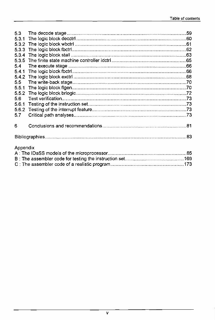
Table of contents
5.3 The decode stage 595.3.1 The logie bloek deeetrl 605.3.2 The logie bloek wbetrl 615.3.3 The logie bloek fbetrl 625.3.4 The logie bloek stall 635.3.5 The finite state machine controller idetrl 655.4 The exeeute stage 665.4.1 The logie bloek fbetrl 665.4.2 The logie bloek exetrl 685.5 The write-baek stage 705.5.1 The logie bloek flgen 705.5.2 The logie bloek brlogie 725.6 Test verifieation 735.6.1 Testing of the instruetion set.. 735.6.2 Testing of the interrupt feature 735.7 Critieal path analyses 73
6 Conelusions and reeommendations 81
Bibliographies 83
AppendixA: The IDaSS models of the mieroproeessor 85B : The assembler code for testing the instruetion set. 169C : The assembler code of a realistic program 173
v
chapter 1
1 Introduction.
Introduction
Modern software for personal computers asks for a lot of disk space. Three years agoone would buy a new PC with a harddisk of 100 MegaByte. That was sufficient at thetime but nowadays 10 times that amount is needed. The explosive growth of softwareand information data makes it necessary to store data more efficiently. Software toolslike 'DoubleSpace' have been introduced to compress data when written to hard diskand decompress when read from the disk.Because of the growth of information data, the transport of this data increases also. Theuser of a communication line is charged for the amount of bits which he sends over theline. To decrease the amount of data to be transmitted and to gain speed the data canbest be compressed before it will be transmitted and decompressed at the receivingside.
These techniques are not new and are already used on a large scale. But most of thetime it is done by software, which makes it relatively slow.For his PhD thesis ir. L.C. Benschop has defined a VLSI circuit that can compress anddecompress data in hardware at a speed of 100 Megabit per second.
The VLSI circuit that must be designed has the following features:• Optimised for lossless data compression of typical computer files, like English text
and computer programs.• A speed potentialof 100 Megabit per second or more (rate of uncompressed data).• A compression ratio comparable to that of widely used software methods (2.9
bits/byte).
Apart from these features there is a requirement that the design is sufficiently generic, sothat it can be adapted to specific requirements.
The functionality of the circuit has been analysed and for all functions the optimumimplementation technique has been selected. The resulting architecture consists ofseveral parts including an embedded microprocessor. All functions have been mappedto the architecture.
1.1 Overview of the VLSI design project.
The VLSI circuit operates as a peripheral within a normal computer system. It is usabiewith a wide variety of computer bus architectures, employing a data bus of 8, 16 or 32bits wide. It employs two DMA channels, one to receive the input data and one to writethe output data. The device is programmabie by the host system through 1/0 ports. Itsends interrupts to the CPU in the host system whenever CPU attention is needed. CPUattention is needed for the allocation of new memory buffers for the DMA process, butnot for steps of the compression process itself. The device can either be used forcompression or for decompression, but it can only perform one of the tasks at a time.
1

chapter 1
1.2 Compression methods.
Introduction
The device uses the LZH (Lempel Ziv+Huffman) method, which is a combination of twomethods, sliding window coding (a variation of LZ77) and Huffman coding. The popularPC programs PKZIP, LHA and ARJ are known to use this method. lts compression ratiois considerably worse than that of the most advanced software methods (arithmeticcoding and a method of context modelling), but better than either Huffman coding orLempel-Ziv coding perform alone. At the moment, very high speed implementation ofmethods that perform better than LZH seems infeasible.The format of the compressed data is compatible with that of the data produced by theLHA program.True dynamic Huffman coding has been considered, but its algorithmic complexity wasfound too high for the required speed. Static Huffman coding is used. This means thatblocks of data are collected and for each block the Huffman code is computed from thefrequency statistics.
host epu DMAcontrol host RAM Host System
.....---ext bu_-----
Compression Processor
figure 1.1. The main madules af the VLSI circuit far data campressian and decampressian.
1.3 The architecture.
The device contains the following main modules as can be seen in figure 1.1:
2

chapter 1 Introduction
• Bus interfaceIt reads the input data and writes the output data through two DMA channels ofthe host computer. Further it communicates with the host computer through 1/0registers and interrupts.
• Sliding window coderIt performs compression or decompression using sliding window coding.
• Buffering and statistics moduleIt stores blocks of lengths, literals and addresses into a separate external RAMand retrieves them later. When storing the data, it compiles frequency statistics.When the device is decompressing, the modules pass the data, using the externalmemory as a FIFO (first in/first out).
• Huffman coderIt performs Huffman coding or decoding of lengths, literals and addresses, usingcode descriptions stored in a RAM. It also enables the internal processor to sendand receive bit fields in the compressed data stream.
• Internal processorIt contrals all other main modules, it performs the Huffman tree computation and itsends and receives Huffman tree descriptions in the compressed data. Note thatHuffman tree computation can be performed efficiently in software.
Sliding window coding, Huffman tree computation and Huffman coding are the stages ofa high-level pipeline. They are performed concurrentlyon different data blocks.
There is an internal processor bus to which all main modules are connected. The othermain modules have 110 ports through which they are controlled and give status. Themodules can also generate internal interrupts. The internal processor is the only busmaster on the internal processor bus. Only the bus interface module is connected to thehost system bus.
This report contains the design of the embedded microprocessor. Chapter 2 describesthe specifications of the microprocessor and the main parts it must contain. It will have aRISC architecture (reduced instruction set computing) and the instruction set andencoding is given. Chapter 3 describes the design of the datapaths that conneet themain parts of the microprocessor, necessary to execute the instructions. To gain speedthe microprocessor is given a pipelined architecture. The modifications to the datapathnecessary to implement these pipelines are shown in chapter 4. A high-level design tooiis used to implement the design. This is shown in chapter 5. It also contains an analysesof the critical paths. The final chapter gives the conclusions and recommendations.
3

chapter 2 The microprocessor specifications
2 The microprocessor specifications.
This chapter contains the specification of the embedded microprocessor as proposed byir. L.C. Benschop. Section 2.8 contains some modifications on the original specifications.
2.1 Introduction.
Many ASICs perform tasks whose functionality is best implemented in software. Theytherefore contain a programmed embedded processor. This processor is integrated intothe ASIC and it is not accessible from outside.
In a complex system we can distinguish several types of tasks.
• High rate tasks that cannot be performed at the required speed by a programmabiecomputer. Dedicated hardware is needed to perform these tasks. The dedicatedhardware performs a single or very few different operations at high speed. Sometimesmany operations are performed in parallel.
• Intermediate rate tasks. These tasks can be performed by a programmed computer. Ifthey are repetitions of a single operation they are usually not implemented that way asa complex device is tied up nearly all the time by a simple operation. If these tasks arevery complex, they are implemented by a computer. The computer often has to havespecial capabilities, for example with digital signal processing.
• Low rate tasks. Any embedded processor has enough computing power to handlethese. These tasks would usually require certain 110 facilities and an interruptcapability of the processor.
The processor to be designed must perform the intermediate rate, high complexity tasksof a lossless data compressor and decompressor. More specifically it must generate theoptimum Huffman code from statistics of the data. Further it must encode and decodedescriptions of these Huffman codes. These descriptions are included with thecompressed data. Finally it must program the code into the Huffman encoding anddecoding hardware. These algorithms use simple operations (like addition) and nomultiplication or division. They do frequently access arrays in a random order. Thereforearray indexing must be very efficient. Speed requirements are high for anembedded processor.
As the designed processor is the only processor in the device, it will also handle the lowrate tasks. We decided not to use a second processor for the low rate tasks for thefollowing reasons.
• The task performed by the device is not real-time. It is therefore acceptable that theintermediate rate tasks are interrupted for a short time to perform low rate tasks.
• The processor already needs a fairly extensive 110 capability to perform theintermediate rate tasks.
5
chapter 2 The microprocessor specifications
This section is a specification for a processor that meets the following requirements.
• The word size and the size of the addressable memory are adapted to the tasks thatmust be performed.
• The instruction set is adapted to the tasks that must be performed. Multiplication anddivision are left out whereas some unusual instructions are included.
• The processor must run at a very high speed.
• Addressing modes are optimised for random access of arrays.
• The instruction set is general enough to be used for typical low-rate control tasks.
• The processor interfaces to the rest of the system.
• It must be implemented in IDaSS and/or VHDL so it can be integrated into the rest ofthe design.
2.2 Overview of the architecture.
The proposed processor has a Harvard architecture. This means that the programmemory and the data memory are separate. Instructions and data can be accessed atthe same time. The program memory is a ROM and the data memory is a RAM. A smallpart of the data address space will be mapped to 1/0 devices.
Operations of up to 16 bit quantities are required, hence the data registers and memorylocations are 16 bits wide. The proposed instruction encoding requires an instructionwidth of 16 bits as weil. Program addresses are Iimited to 12 bits, but the only basis forthis limitation is the encoding of the jump and jsr instructions. Extension to 13 or even 16bits should be possible, if necessary. Data addresses are 16 bits, but they could bereduced, e.g. to 12 bits if that is sufficient. In the proposed application 12 bits would besufficient. As a consequence the base registers and stack pointer could all be reduced to12 bits.
The processor would have the following registers.
• index base registersThere are up to 16 index base registers. They are added to an index register toobtain the address in indexed addressing mode. These registers are typically set tothe start address of an array and remain constant during the execution of analgorithm. The index registers are used as the array index and vary far morefrequently.
• direct base registersThere are up to 2 direct base registers. They are added to a 6-bit direct address toobtain the address in direct addressing mode. These registers are typically set to amemory area for various variables and the 1/0 address area respectively.
6

chapter 2 The microprocessor specifications
The direct addressing mode is then used to address either one of 64 variables orone of 64 I/a ports.
• general purpose registersThere are up to 8 general purpose registers. Arithmetic and logic operations alwayshave a general purpose register as the destination. One of the source operands isthe same register as the destination and the other source operand is either ageneral purpose register, a memory operand, or an immediate value. Generalpurpose registers also serve as index registers in indexed addressing mode. If theword 'register' is used in this paper, its default meaning is one of the generalpurpose registers.
• program counterThe program counter addresses an address in ROM where the next instruction willbe loaded from.
• stack pointerThe stack pointer addresses the top of stack in RAM. The stack will grow downwardas registers or return addresses are pushed on it. The stack is used by thepush/pop instructions, the jsr/rts instructions and by interrupts.
• status flagsThe status flags indicate the result of the last compare instruction, whether theresult of the last instruction was zero or whether the result of the last instructionwas all bits set.
The execution of an instruction takes the following steps.
• Fetch the instruction from ROM at the program counter address.• Decode the instruction.• Get the values of the register operand(s).• Compute the address of the memory operand and address the memory.• Get the value of the memory operand.• Compute the result.• Increment the program counter or assign a new value to it Uump).• Store the result in a register if appropriate.• Store the appropriate flag values.• Check for interrupt, if it occurs save program counter and status flags, reload program
counter with start address interrupt routine.
Many of these steps can be combined into one cycle by using combinatoriallogic and pipelining.
The following operations will each take a clock cycle.
• Accessing the RAM for either reading or writing.• Actually storing values in registers.• Accessing the ROM for reading an instruction.
7

chapter 2 The microprocessor specifications
Each instruction accesses only one RAM location (either reading or writing), reads onlyone ROM location and modifies at most one register, not counting stack pointer, programcounter or status bits.By careful design it should be theoretically possible to finish each instruction in exactlyone cycle. A practical pipelined processor will have certain inter-instructiondependencies that require at least one cycle between them.
2.3 Memory and 1/0 interfacing.
The processor has the following connections to the rest of the system.
• dataThis is a 16 bit wide bi-directional bus. It carries all data from and to the RAM andthe 110 devices.
• addressThis is a 12 bit wide bus driven by the processor. It carries the address of the RAMlocation or the 1/0 device that is accessed.
• readThis is one line driven by the processor. If set high, the RAM (or the addressed 1/0port) must place a value on the bus at the next clock edge.
• writeThis is one line driven by the processor. If set high, the RAM (or the addressed 1/0port) must accept the value on the data bus at the next clock edge.
• interruptThis is an input \ine for the processor. If it is high at the active clock edge, theprocessor interrupts its normal program flow.
The ROM is part of the processor itself and the connections to it are notdescribed here.
The external interface is similar to a traditional processor bus, except that it is asynchronous design in which all bus cycles take exactly one clock cycle. If an address isplaced on the address bus along with the read and write signais, the addressed data(either read from RAM or written to RAM) appears on the data bus during the next clockcycle and by that time the next address may already appear.
An address decoding circuit will decode the address into the signals necessary to selectthe various pieces of RAM and 110 devices. This decoder is primarily a combinatorialcircuit. In the designed system a 4 kiloword address range is expected, divided into thefollowing regions.
• 2 kilowords of RAM that is only accessible by this processor.
• About 1 kiloword of RAM that is swappable between the processor and the Huffmanencoder/decoder. There are two 'banks' of this RAM, one being exclusively accessibleby the Huffman coder and the other being exclusively accessible by the processor.While the Huffman coder uses one of the memory banks, the processor prepares theother bank for the next set of codes. The banks are swapped by setting one input tothe address decoding circuit.
8

chapter 2 The microprocessor specifications
• About 0.5 kilowords of RAM that is swappable between the processor and thestatistics collecting module.
• A 16 byte 'parameter RAM', which is shared between the processor and the businterface of the device.
• Various control, status and other ports of the other modules. These are the 110addresses, preferably mapped to one consecutive range. It is expected that less than64 addresses are needed.
2.4 The instruction set.
The proposed processor must have the following instructions. The mnemonics of similarinstructions on widely used processors are used.
add Add, binary operation.
and Logical bitwise and, binary operation.
emp Compare, destination is not changed, only flags indicate whether destinationwas above, below or equal to the source operand, using unsigned binaryarithmetic.
epi Complement register (unary operation).
djnz (optional) Decrement a register and jump if it was not zero.
ja Jump if flags indicate Above.
jae Jump if flags indicate Above or Equal.
jb Jump if flags indicate Below.
jbe Jump if flags indicate Below or Equal.
je Jump if flags indicate Equal.
jmp Jump to ROM address.
jne Jump if flags indicate Not Equal.
jns Jump if All-set flag is not set.
jnz Jump if Zero flag is not set.
js Jump if All-set flag is set.
jsr Jump to subroutine at ROM address, push old program counter on stack.
9

chapter 2
jz Jump if Zero flag is set.
The microprocessor specifications
mhi Move immediate data to high 8 bits of destination register.
mov Move source operand to destination operand. Both can be registers, the sourcecan be a memory or immediate operand, in which case the destination is aregister. The destination can be a memory operand, in which case the sourcemust be a register. If either of the operands is a non-general purpose register(base register, stack pointer), the other operand must be a general purposeregister. As opposed to other instructions, mov occurs in many differentinstruction formats.
or Logical bitwise or (binary operation).
pop Pop a register from the stack (unary operation).
push Push a register onto the stack (unary operation).
rti Return from interrupt.
rts Return from subroutine.
set Set register to all ones (unary operation).
shl8 Shift a general purpose register left 8 places (unary operation).
shr Shift a general purpose register right (unary operation). There is no shl, becausean add of the register to itself already does this.
shr8 Shift a general purpose register right 8 places (unary operation).
sub Subtract source from destination (binary operand).
xor Logical bitwise xor (binary operation).
Next to these instructions there are three more application specific instructions: sel2,sel3 and the till operation. They will be discussed in section 2.5.
The instructions fall into several categories.
• Binary operationsThese are add, sub, and, or, xor, cmp, mov and mhi. There are 8 binary operations.mhi only occurs with immediate addressing. With the other addressing modes thereare two different forms of mov, one to move the source operand to the destinationregister (Ioad) and one to move the destination register to memory at the addressof the source operand (store). With register to register operations, only sevenbinary operations are possible.
10

chapter 2 The microprocessor specifications
• Unary operationsThese are epi, pop, push, set, shl, shr and shr8. These operations have oneregister as an operand. Up to 16 different unary operations can be specified. pushand pop access memory and modify the stack pointer.
• Jump operationsThese are djnz, ja, jae, jb, jbe, je, jmp, jne, jns, jnz, js, jsr and jz. jmp and jsr have a12 bit address that can be any ROM /ocation. The other jump operations specify an8-bit signed displacement with respect to the current program counter. At thisstage of the specification it is not important whether or not the program counter wasalready incremented before the displacement is added to i1.
• Other operationsThese are rti, rts and other application specific instructions.
The binary operations have the following possible addressing modes.
• register to registerThe souree operand and the destination operand are both registers.
• direct addressingThe destination operand is a register and the souree operand is in memory at anaddress that is the sum of a direct base register and a 6-bit address specified in theinstruction. There are two directly addressable areas of 64 locations each. One ofthe areas will be used to store certain variables and the other one will be the 1/0area.
• indexed addressingThe destination operand is a register and the souree operand is in memory at anaddress that is the sum of an index base register and a general purpose register(used as index register). This is the primary mode to access arrays.
• immediate addressingThe destination operand is a register and the souree operand is an 8-bit value. Thehigh bits of this value are O. mov with an immediate operand sets the high bits ofthe destination to zero. mhi sets the high bits of the destination register to theimmediate value and leaves the low bits unchanged.The proper way to set r1 to the value 1234h is therefore
mov r1,34hmhi r1,12h
The logical operations with immediate addressing are often needed to selectcertain flag bits in 110 operations. Therefore we willlimit the width of 1/0 ports withflag bits to 8 bits.
11

chapter 2 The microprocessor specifications
A possible encoding for the instruction set with each instruction fitting in 16 bits is shownin table 2.1. The fields have the following meaning.
addr12
bd
basei
bop
cond
direct6
disp
imm8
jop
regd
regi
regs
uop
12-bit address in jmp or jsr instruction.
1-bit direct base register specifier.
4-bit index base register specifier.
3-bit specifier for binary operation.
4-bit specifier for jump condition.
6-bit direct address.
a-bit signed displacement in jump conditions.
a-bit immediate value.
1-bit specifier to select jmp to jsr.
3-bit specifier for destination register.
3-bit specifier for index register.
3-bit specifier for source register.
4-bit specifier for unary operation.
It is not required (maybe not desirabie) to use the exact same encoding, butthis one shows that it is possible to encode all instructions in 16 bits.
Table 2.2 contains the encoding of the several fields of the instructions.
12

chapter 2 The microprocessor specifications
--...;.;;....;-------disp8-...;-~-- x --regd--
1 1 0 0 x x x x x ----uop---- --regd-- Unary operation
1 1 0 1 x x x --regs-- --bop--- --regd-- Binary operation, register
1 1 1 ---basei--- --regi-- 0 0 0 --regs-- FILL
1 1 1 ---basei--- 0 0 0 0 0 1 --regs-- Movto base register. . ........
1 1 1 x x x x 0 bd 1 0 0 1 --regs-- Movio direct base reg
1 1 1 x x x x 1 0 0 0 0 1 --regs-- Mov to SP
1 1 1 x x x x x x x 1 1 0 x x x RTS
1 1 1 x x x x x x x 1 1 1 x x x RTl
table 2.1. One way to encode the instructions.
13
chapter 2 The microprocessor specifications
.. ".. . .
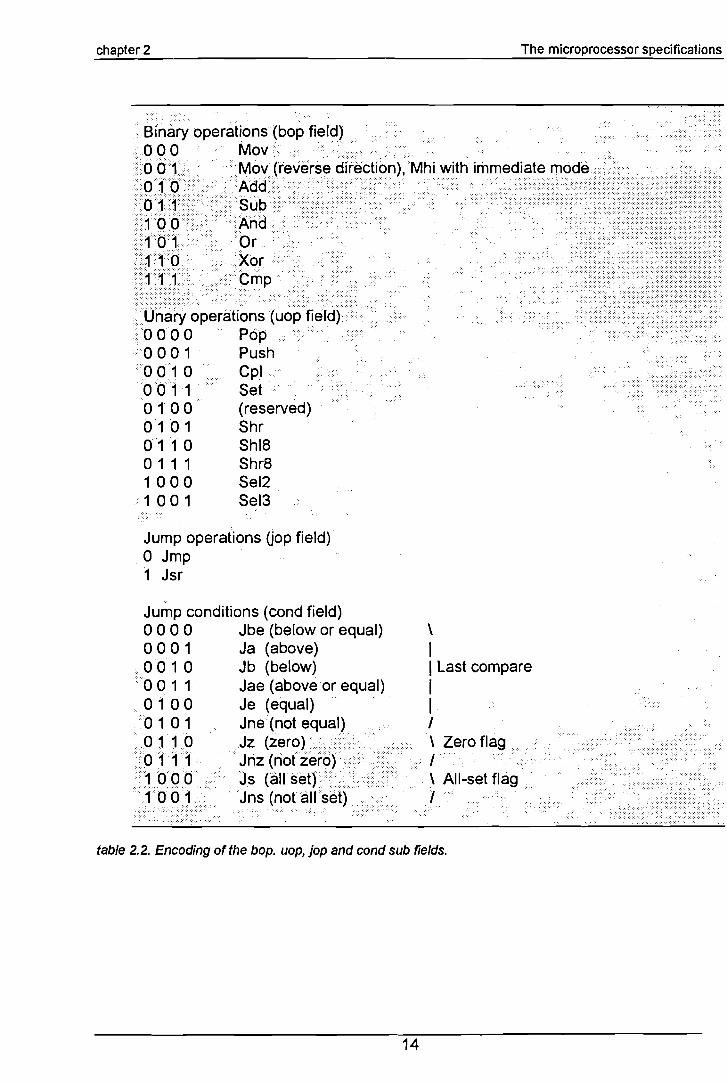
. Binaryoperalions(bop field) ....'.. 0 0 0 Mov '.,. ..' ,.....".'.'.'./' .....
bêf1, ... ... Mov(r'everse cfiiéetion),Mhi with immediate
Il:IIlliiii;;~~!~::::tt > Ct ti iii >< >< >
111 .. <Cmp
lJn~~~p:rati~ns(uop tleIICll·/·'·
,<0 00 0 Pöp/0 0 0 1 Push001 0 C I... ..... P0011 Seto1 0 0 (reserved)010 1 Shr01 1 0 Shl8o1 1 1 Shr81 0 0 0 Sel21 0 01 Sel3
Jump operations GoP field)o Jmp1 Jsr
Jump eonditions (eond field)o0 0 0 Jbe (below or equal)o0 0 1 Ja (above)
." .. 0 0 1 0 Jb (below)00 1 1· Jae (aboveor equal)01 0 0 Je (equal)
.0 10 1 Jne (not equal)o 1·1,0 Jz (zero).,,> />
Io1·1·1 ,.,. Jnz (riofzef6) .. » ,,•••••••••••••• ,.1ÓO0 .. Js (all set) >
'·'ro or Jns(notallset)/ ...
\II Last eompareIII\ Zero flagI
. \ All-set flagI /'
tab/e 2.2. Eneoding of the bop. uop, jop and eond sub fie/ds.
14

chapter 2
2.5 Application-specific instructions.
The microprocessor specifications
For the specific application of Huffman tree computation the following specialinstructions are desired.
fill Fill a memory region with a certain value. The value is in the source register.The memory region is specified by an index base and an index register. Thesource register is stored in memory at the address that is the sum of the indexbase register and the index register. Then the index register is decremented byone. If the index register is decremented below zero (it then contains all 1 bits),the instruction terminates, else the instruction does not increment the programcounter and repeats itself.This way a region could be filled one location per clock cycle.
sel2 Select second field (unary operation). Shift the destination register right fourplaces and 'and' with 15.
sel3 Select third field (unary operation). Shift the destination register right eightplaces and 'and' with 31.
2.6 Interrupts.
When the microprocessor is reset it starts execution at ROM address O. When aninterrupt occurs, the program counter and status bits are saved and execution proceedsat ROM address 1. The rti instruction restores the program counter and status bits thatwere saved by the interrupt. Only one interrupt is planned. The interrupt handier wouldpoll the various possible interrupt sources to see which event caused it. 8etween aninterrupt and an rti, the interrupt is disabled.
As program addresses are 12 bit and there are four status bits (two for compare result,an all-set flag and a zero flag), it would be possible to combine them in one 16-bit wordand push that onto the stack.
Alternatively one can use a special-purpose register to save the program counter andstatus bits.
2.7 Variations.
It would be possible to simplify the processor considerably if the following modificationscould be carried out.Whether these variations are acceptable is highly dependent on the program that is runon the processor. It is probably only known after the software is written.
15

chapter 2
The following variations are proposed.
The microprocessor specifications
• Leave out the stack pointer, the push and pop instructions and the jsr/rts instructions.For the interrupt facility use a special-purpose register to save the program counterand the status.
• Hardwire all or some base registers to fixed locations. These registers can than bereplaced by ROM cells, or even a combinatorial circuit. For the direct base registers,this is almost certainly possible.
2.8 Modifications and supplements to the original concept.
This section describes the modifications made to the original concept during the courseof the design.
2.8.1 Changing to a load-store architecture.
All binary operations can also be pertormed on data which comes directly from the DataMemory. When implementing pipelines in the design it became clear that there were twoextra pipeline stages necessary to make this possible. These extra pipeline stageswould cause some extra stalling of the throughput of the pipeline. Therefore the decisionwas made to change the concept and to give the processor a load-store architecture.This means that no operations can directly be done on data coming from or going to theData Memory.If an operation must be pertormed on data from the Data Memory, this data must first betransferred to one of the General Purpose Registers. Then the operation can bepertormed on the data after which it will be written back to one of the General PurposeRegisters. Then this result can be written back to the Data Memory.
2.8.2 Changing the suggested encoding of the instructions.
In the assignment suggestions were made for the instruction encoding. After a closerstudy some changes have been made.
The suggested encoding of the instructions for "direct binary operations" and for "moveto direct base register" were:
15 14],3 12 11 10 9 8· 7 6 5 4 3 2 1 0 ...< ..
(»01l:>ef--..;--ctlrect6----- -..;bop~~- --regd-- Binary operatiml,dirê2t
1 11) x x x x 0 bd 10 0 1 "'--regs-- Mov to direct base règ .....
As bit 12 of the "mov to direct base reg" is a don't care it would be more logical to usethat same bit for assigning which direct base register is to be used.
16
chapter 2
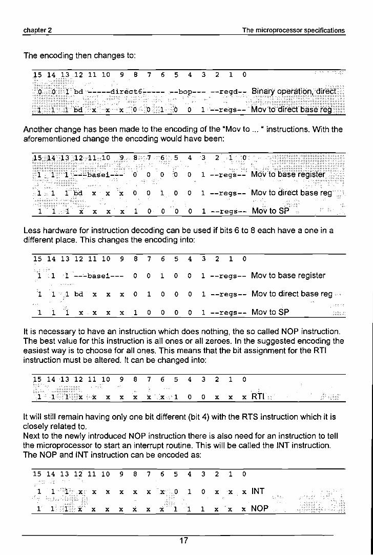
The encoding then changes to:
The microprocessor specifications
15 1413 12 11 10 9 8 7 6 5 4 3 2 1 o
f)ië» 1 bd -----direct6...----,..-bop--,.. --regd~~ Biriary op~rátiÓl'1igir~çf
Another change has been made to the encoding of the "Mov to ... 11 instructions. With theaforementioned change the encoding would have been:
151413121L109
ii1t----B~s~~-iS1 1bd x x x
8 >7 6 5 4 3 2 1 0
0 0 0 <0 0 1 --regs--:
1
::::.:».:::<>11 x x x x
o
1
01
o 0
o
o
o
o
·M'··""··"·':"'·;t>ibIC~t·························••••••••••••••.. ".ov 0 ase reglser«
1 --regs--MOv to direct base reg••• • •• 0.
1 --regs-- Mov to SP
Less hardware for instruction decoding can be used if bits 6 to 8 each have a one in adifferent place. This changes the encoding into:
15 14 13 12 11 10 9 8 7 6 5 4 3 2 1 0
11 1 ---basei--- 0 0 1 0 0 1 --regs-- Mov to base register
1 1 ·'··1· bd· x x x 0 1 0 0 0 1 --regs-- Mov to direct base reg
1 11 x x x x 1 0 0 0 0 1 --regs-- Mov to SP
It is necessary to have an instruction which does nothing, the so called NOP instruction.The best value for this instruction is all ones or all zeroes. In the suggested encoding theeasiest way is to choose for all ones. This means that the bit assignment for the RTlinstruction must be altered. It can be changed into:
1 5 1 4 1 3 1 2 1 1 1 0 9 8 7 6 5 4 3 2 1 0,, ,,, ,
Ril1 1 i< x /"·'·x x X X X x 1 0 0 x x x ,, ,
It will still remain having only one bit different (bit 4) with the RTS instruction which it isc10sely related to.Next to the newly introduced NOP instruction there is also need for an instruction to teilthe microprocessor to start an interrupt routine. This will be called the INT instruction.The NOP and INT instruction can be encoded as:
15 14 13 12 11 10 9 8 7 6 5 4 3 2 1 0
1 1 ····"·"1·"',·..,x 0 1 0 INT.. x"· x x x x x x x x
.. : ... ::>.".
1 1 1 x x x x x X x 1 1 1 x x x NOP
17

chapter 2 The microprocessor specifications
The complete encoding as will be implemented is shown in table 2.3.
........ ' .... -..:
151413 1:2 11 10 98 76 54 3 2 1 0
0··· 0 ····.0 ·L~-basei--'- --re9'i-~ ·-~bop--- --regd-- Binaryoperati6r1,igde~èèr·••••••••ö••••••••·.··6·....·.· ••·••i·•••• b&·······~-'-·~:dii~cf.g:L·~î2·· ·.~·îbop--- --iegd~-. ·f3ir1~~···op~f~ii·8R, ••••8if~·gt ••••••••••••••••••••••••••••.
/6<1 ...~2~l_- __·-----f~8--20=L~ ... ~~bbp--- -~regd~~ B. i~~ry··.·.·. ()p<e.i.(~.~ti6ri,. i.m.··.···.·•.·.·.m.··.·.·.·••.· ••.·.~·.di~t~U}/::: ' "
1 <l.·•• l() ~.~----------disp8---------cond---- condition~I]U~6i·.
DJNZL 0 1 1 ------------disp8------ x --regd--
1 1 0 0 x x x x x ----uop---- --regd-- Unary operation
1 1 0 1 x x x --regs-- ~-bop--- --regd-- Binary oper~tion, register
·1··· 1 1 -'--basei--- --regi-- 0 0 0 --regs-- FILL
1 1 1 ---basei--- 0 0 1 0 0 1 --regs-- Mov to base register
1 1 1 bd x x x 0 1 0 0 0 1 --regs-- Mov to direct base reg
1 1 1 x x x x 1 0 0 0 0 1 --regs-- Mov to SP
1 1 1 x x x x x x x 0 1 0 x x x INT
1 ....... 1 1 x x x x x x x 1 0 0 x x x RTl
je x x x x x x 1 1 0 x x x RTS
1 1 1 x x x x x x x 1 1 1 x x x NOP
table 2.3. The encoding of the instructions as they will be implemented.
18

chapter 2 The microprocessor specifications
Next to the encoding of the instructions are some modifications made to the encoding ofthe unary operations. The suggested encoding was:
Unaryoperatiohs (uop field)
ggg~ ·~3~H/i ... /...••...~g .•~ ..•~ ·~~iio1 0 0 . (résèrved)<010 f SHR .0·110 •........•. ( ·$141...80111 .... ·/SRR8
<1ÓÖOSEL2.1Ö01 SEL3
From these instructions only the POP and the PUSH operation are not using the ALU.The binary operations consist of 8 different ALU-operations. The unary operations alsohave 8 different ALU-operations. By changing the first bit of the unary operationsneeding the ALU into a one, it is easier to generate the control signals for the ALU.Binary operations will start with a zero and unary operations will start with a one.The encoding also has one encoding free (reserved). This will be used for the'decrement' operation which is necessary in case of an DJNZ instruction.The new encoding will now be:
Unary operations (uop field)0000 POP0001 PUSH1 01 0 CPL1 01 1 SET1 100 DEC1 1 01 SHR
.... 1 1 10 SHL8· .·1·1 1 1 SHR8
1 000 SEL21001 SEL3
As the dec operation is added for the djnz instruction this unary operation can now alsobe used as an extra instruction.The binary operations have two possible MOV operations: one to transfer data from oneof the General Purpose Registers to the Data Memory and one to transfer data the otherway. To make it more clear which is which:
bop field . .........•.....................000 MOV is used for data transfer from memory to a register (Ioad)001 . MOV is used for data transfer from a register to memory (store) .i
19
chapter 2 The microprocessor specifications
One encoding which was failing from the suggested encodings was the flag assignment.The assignment will be:
flagbit 0 :Jlà9pif 1:f1ágbif2:
/flaghif 3 :.
. all zeroallset .
. 5mallèr .....•.. .greatér··•••...•...•.•
The 'smaller' and 'greater' flags will only be changed by a CMP instruction (compare).No flag will change by the instructions JMP, JSR, RTS, NOP, INT and one of theconditional jump instructions, except for the DJNZ instruction which is able to change thef1ags.In case of an interrupt the return address will be saved on the stack together with theflags. On a 'return from interrupt' all flags will be restored from memory.
2.8.3 The displacement in case of a conditional branch instruction.
In section 2.4 the specification left open whether or not the program counter wasincremented before the displacement is added to it in case of a conditional branchinstruction. In the final design in case of a conditional branch instruction thedisplacement is added to the incremented program counter contents.
2.8.4 The bidirectional databus changed to two separate busses.
In the specification the external databus of the embedded microprocessor is abidirectional databus. The disadvantage is that the bus can not write to the Data Memoryone clock cycle after it has done a read operation from that Data Memory as bothoperations then need the databus at the same time.To prevent these unnecessary stalIs and extra tri-state buffers the databus is separatedinto a data-input-bus and a data-output-bus.
20
chapter 3 Designing an architecture for the embedded processor
3 Designing an architecture for the embeddedprocessor.
This chapter will describe the steps which were taken in designing this microprocessor.During the course of the design the decision was made to give the processor a loadstore architecture. This means that no operations can directly be done on data comingfrom the Data Memory. To show why this decision was made the original idea will first beworked out. When appropriate I will change to the load-store concept.
The processor will contain the following major parts:• an Instruction Memory (4Kx16 ROM)• a Data Memory (4Kx16 RAM)• 8 General Purpose Registers (GPR)• 16 Index Base Registers (IBR)• 2 Direct Base Registers (DBR)• 1 Stack Pointer Register (SPR)
The first step is to construct a datapath to interconnect all these parts. This is doneaccording to the design concept presented by Patterson and Hennessy in [Pat94]. Areasonable way to start a datapath design is to examine the major components requiredto execute each type of instruction. By looking at which datapath elements eachinstruction needs the sections of the datapath will be built up from these elements foreach instruction type. When the datapath elements are shown initially, the controlsignals will be shown. To prevent the figures to be blurred by all the control signals theywill be left out until the final datapath will be presented.
The instructions fall into several categories:• binary operations• unary operations• jump operations• other operations
3.1 Constructing a datapath for the program counter.
A 12 bit register can be used as the Program Counter (PC). The program counteraddresses the instructions, which are stored in the Instruction Memory (Read OnlyMemory). The program counter can be incremented by an adder to be able to addressthe next instruction. The datapath for this part is shown in figure 3.1.
3.2 Constructing the part of the datapath for the binary operations.
The binary operations are add, sub, and, or, xor, emp and mov. These operations,except for mov, can best be performed by an ALU. As can be seen in table 2 the movoperation has two different encodings and wil! be explained for each addressing mode.
21

chapter 3
wn"te
Designing an architecture for the embedded processor
InstructionMemory
4Kx16
12 ProgramCounter
1----.1__12+ __-1 address dàta out 16
instruction
figure 3.1. A part of the datapath used for fetching instructions and incrementing the program counter.
The binary operations can be divided into the following addressing modes:• register to register• direct addressing• indexed addressing• immediate addressing
3.2.1 Register to register binary operations.
The two operands both come from a General Purpose Register. The ALU performs anoperation on the data. The result of the operation is always wriUen back to source one ofthe source registers. This results in a datapath as shown in figure 3.2.In case of the mov operation, the ALU functions as a multiplexor and only passes thedata. The data can only be copied (mov) from source2 to source1 (destination). For thismov operation the encoding 000 will be used. The movencoding 001 will not be usedwith this addressing mode.
write
3 sourcelldestination data1
Generalsource2 Purpose
Registers
data in data2
ALUop
1o-__ f1ag
16
figure 3.2. The datapath for register to register binary operations.
22
chapter 3 Designing an architecture tor the embedded processor
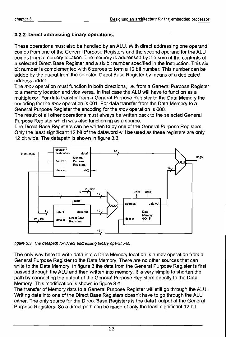
3.2.2 Direct addressing binary operations.
These operations must also be handled by an ALU. With direct addressing one operandcomes from one of the General Purpose Registers and the second operand for the ALUcomes from a memory location. The memory is addressed by the sum of the contents ofa selected Direct Base Register and a six bit number specified in the instruction. This sixbit number is complemented with 6 zeroes to form a 12 bit number. This number can beadded by the output from the selected Direct Base Register by means of a dedicatedaddress adder.The mov operation must function in both directions, Le. from a General Purpose Registerto a memory location and vice versa. In that case the ALU will have to function as amultiplexor. For data transfer from a General Purpose Register to the Data Memory theencoding for the mov operation is 001. For data transfer from the Data Memory to aGeneral Purpose Register the encoding for the mov operation is 000.The result of all other operations must always be written back to the selected GeneralPurpose Register which was also functioning as a source.The Direct Base Registers can be written to by one of the General Purpose Registers.Only the least significant 12 bit of the dataword wil! be used as these registers are only12 bit wide. The datapath is shown in figure 3.3.
source1/ 16instruction destination data1
Generalsource2 Purpose
Registers
data in data2
address data out
write read6
L...--+--I select
....-.;.:12r-1S.;..b_-I data in
data out t-_12-+--IDirect BaseRegisters
16
data in
DataMemory4Kx16
figure 3.3. The datapath for direct addressing binary operations.
The only way here to write data into a Data Memory location is a mov operation from aGeneral Purpose Register to the Data Memory. There are no other sources that canwrite to the Data Memory. In figure 3 the data from the General Purpose Register is firstpassed through the ALU and then written into memory. It is very simple to shorten thepath by connecting the output of the General Purpose Registers directly to the DataMemory. This modification is shown in figure 3.4.The transfer of Memory data to a General Purpose Register wil! still go through the ALU.Writing data into one of the Direct Base Registers doesn't have to go through the ALUeither. The only source for the Direct Base Registers is the data1 output of the GeneralPurpose Registers. So a direct path can be made of only the least significant 12 bit.
23
instruction
chapter 3 Designing an architecture for the embedded processor
source1/ 16r----t destination data1 t---......,I....--r-----------t
Generalsource2 Purpose
Registers
..---+---1 data in data2
12 Isb
60 data in data out
Data
addressMemory4Kx16
12data in data out
select Direct BaseRegisters
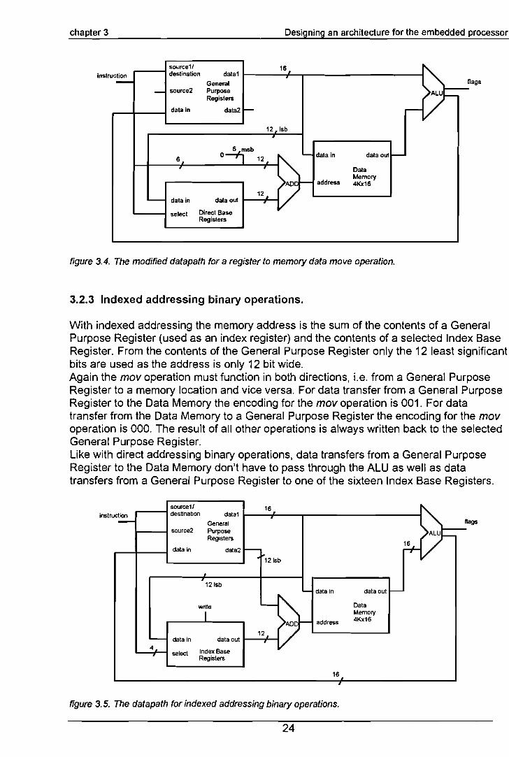
figure 3.4. The modified datapath for a register to memory data move operation.
3.2.3 Indexed addressing binary operations.
With indexed addressing the memory address is the sum of the contents of a GeneralPurpose Register (used as an index register) and the contents of a selected Index BaseRegister. From the contents of the General Purpose Register only the 12 least significantbits are used as the address is only 12 bit wide.Again the mov operation must function in both directions, i.e. from a General PurposeRegister to a memory location and vice versa. For data transfer from a General PurposeRegister to the Data Memory the encoding for the mov operation is 001. For datatransfer from the Data Memory to a General Purpose Register the encoding for the movoperation is 000. The result of all other operations is always written back to the selectedGeneral Purpose Register.Like with direct addressing binary operations, data transfers from a General PurposeRegister to the Data Memory don't have to pass through the ALU as weil as datatransfers from a General Purpose Register to one of the sixteen Index Base Registers.
source1/ 16instruction destination data1
Generalsource2 Purpose
Registers
data in data2
121sb
121sb
write
12data in data out
4Index BaseselectRegisters
data in
address
16
data out
DataMemory4Kx16
figure 3.5. The datapath for indexed addressing binary operations.
24

chapter 3 Designing an architecture for the embedded processor
From the data written to a selected Index Base Register only the least significant 12 bitsare used as the Index Base Registers are only 12 bit wide.The resulting datapath for indexed addressing is shown in figure 3.5.
3.2.4 Immediate addressing binary operations.
With immediate addressing one operand is the contents of a General Purpose Register.The lower a bits of the other operand is part of the instruction and the upper a bits aremade zero. The result of the binary operation is written back to the selected GeneralPurpose Register.In case of a mov operation with encoding 000, the a-bit value from the instruction (bits 6to 13) will be used as the least significant bits of the result. The a most significant bitsare made zero. This result will be written to the destination register. The other movoperation with encoding 001 will here be called an mhi instruction (move high).In case of an mhi instruction the a-bit value from the instruction will replace the upper abits of the source/destination register and leaves the lower bits unchanged.With the register-to-register, indexed and direct addressing modes the mov operationwith encoding 000 pass the data through the lower part of the ALU. The mov operationwith encoding 001 has so far not been going through the ALU. To keep the ALU assimpIe as possible it would be convenient to have all mov and mhi operations passthrough the lower input port of the ALU. A possible implementation for the datapath ofthis addressing mode is given in figure 3.6.
8
source1/instruction destination data1
General tlagssource2 Purpose Isb
Registers
data in data2
figure 3.6. The datapath for immediate addressing binary operations. Both mov and mhi operations passthrough the lower input port of the ALU.
Another possible solution is to have the mov operation pass through the lower input portof the ALU and the mhi operation pass through the higher part of the ALU. Themultiplexor wil I merely move to the other input of the ALU and the same amount ofhardware is needed. This is shown in figure 3.7.It is now quite clear that hardware can be saved. The lower a bits of the dataword for theupper part of the ALU must always pass unchanged. If the 16-bit dataword is split intotwo a-bit parts then only the upper a bit need to be multiplexed.The multiplexor now only needs to be half the size. This is shown in figure 3.8.
25

chapter 3 Designing an architecture tor the embedded processor
8
instructien
seurce1/16destinatien data1
Generalseurce2 Purpese
Registers
data in data2
f1ags
16
figure 3.7. The mhi operation now passes the data through the upper input port of the ALU.
Isb 8
flag
msb 8o
8
data1 t-1_6.J--I----&__m_sb---.,8f----.......-....,.-I
GeneralPurpeseRegisters
d~ain da~2
seurce1/t----I destinatien
.....__-1 seurce2
instructien
16
figure 3.8. The databus for the upper input port of the ALU can be split into two parts of 8 bit.
3.2.5 Putting the parts together tor the binary operations.
AI! the parts of the datapath as we have seen so far can be combined into oneschematic. The direct addressing mode and the indexed addressing mode both sharethe same adder to calculate the effective memory address. A multiplexor for both inputsof the adder wil! make the switching between the two modes possible.Another multiplexor is needed to select the data for the lower ALU input. It must bepossible to select between the immediate number from the immediate addressing mode,the output of the souree 2 register in case of a register-to-register addressing mode andbetween the output of the Data Memory in case of a direct or indexed addressing mode.Each multiplexor wil! have its own control signais. They wil! not be shown here yet.The combined datapaths are shown in figure 3.9.
26

g.Il)
~CD..,W
oCDIn
<5"~,::J
<0Il)::JIl)
g.;::0:CDSlc:alo..,-::rCDCD3C"
~Co
~
ag~o..,
msb
DataMemory4Kx16
8
16
L... -1 data in
..J-_....:.12':./-_--1 address
o
data out
Direct BaseRegisters
data in
select
6
L.. --' 12
Isb
[12)
12 Isb
[11 ..6]
[13..6]
data in data out
[12..9] Index BaseL.;_"';'~ select Registers
[2..0) source1/ 16instruction ~-.;..~ destination data1 I-----------..,.-.....:~--+-.J..-...,,..:;.::..- .....-...;.;r---.....
data out General[8..6)
source2 PurposeRegisters
data in data2
InstructionMemory
4Kx16
1--1.--1 address
ca'§CD
~
!O()030-S'5'
1OSCD~Q)
~0.....
ProgramSCD Counter
~ar~Q)
S0'""'
'"SCD
-.....J 0-S"Q)
~.g
CDii3~:::3~

chapter 3 Designing an architecture tor the embedded processor
3.3 Adding the part of the datapath for the unary operations.
The Unary operations are pop, push, epi, set, shr, shlB, shrB, sel2 and sel3.Except for the pop and push operations all unary operations can be performed by theALU. So there must be a path from the General Purpose Registers through the ALU andback. As this is already implemented for the register-to-register binary operations, nofurther path modifications have to be made.The pop and push operations need a stackpointer. A stackpointer needs to be toaded,incremented and decremented. The contents of the stackpointer addresses a memorylocation of the Data Memory. As the address adder already addresses the Data Memoryanother multiplexor is necessary here. This is shown in figure 3.10.
o
DataMemory4Kx16address
"-----t data in data out
data out
Index BaseRegisters
data out
Direct BaseRegisters
t----I data in
1----1 data in
1---4-_--1 select
'---+-----1 select
6
write incr deer
'----I data in data out 1------------1
Stack PointerRegister
figure 3. 10. Adding the Stack Pointer Register to the datapath.
In this configuration it is quite clear that when the Data Memory is addressed by theStack Pointer Register, the adder is not used. It can be used to increment or decrementthe contents of the Stack Pointer Register. This makes the Stack Pointer Register moresimpte and changes it into an ordinary register.The stack pointer points to the top of stack which is an unused memory location. As thestack pointer points to the next free /ocation, the address pointed to by the stack pointermust be used to address the Data Memory in case of a push instruction. At the sametime the address can be decremented by the address adder and be directed back to theinput of the Stack Pointer Register. At the next clock the decremented data will beclocked into the Stack Pointer Register which will now point again to the next freelocation.In case of a pop instruction the contents plus 1 must be used to address the DataMemory. This value can be extracted from the address adder after it has incrementedthe contents of the Stack Pointer Register. This value will also be written back to theStack Pointer Register.
28
chapter 3 Designing an architecture tor the embedded processor
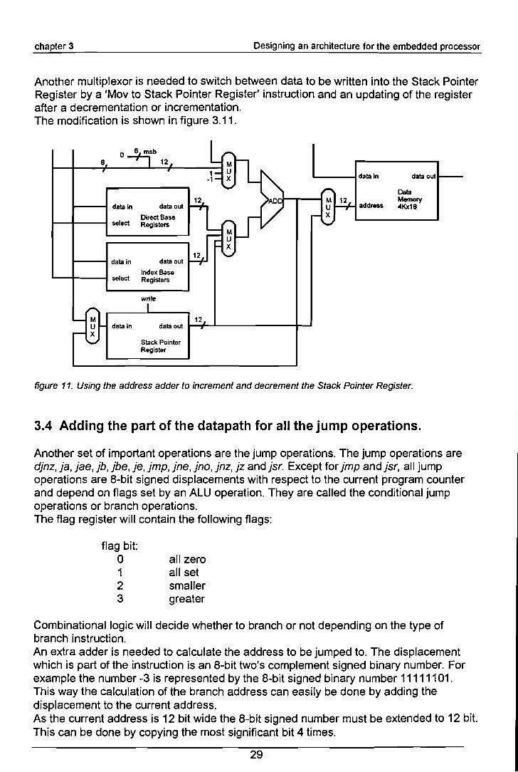
Another multiplexor is needed to switch between data to be written into the Stack PointerRegister by a 'Mov to Stack Pointer Register' instruction and an updating of the registerafter a decrementation or incrementation.The modification is shown in figure 3.11.
0 6 msb
6 12
data in data out
Data12
addressMemory
data in data out 4Kx16
Direct Baseselect Registers
1----1 data in data out
Index Base"'----+----t select Registers
write
12data out ~f--JL....-_------tr----
Stack PointerRegister
figure 11. Using the address adder to increment and decrement the Stack Pointer Register.
3.4 Adding the part of the datapath for all the jump operations.
Another set of important operations are the jump operations. The jump operations aredjnz, ja, jae, jb, jbe, je, jmp, jne, jno, jnz, jz and jsr. Except for jmp and jsr, all jumpoperations are a-bit signed displacements with respect to the current program counterand depend on flags set by an ALU operation. They are called the conditional jumpoperations or branch operations.The flag register will contain the following flags:
flag bit:o123
all zeroall setsmallergreater
Combinational logic will decide whether to branch or not depending on the type ofbranch instruction.An extra adder is needed to calculate the address to be jumped to. The displacementwhich is part of the instruction is an a-bit two's complement signed binary number. Forexample the number -3 is represented by the a-bit signed binary number 11111101.This way the calculation of the branch address can easily be done by adding thedisplacement to the current address.As the current address is 12 bit wide the a-bit signed number must be extended to 12 bit.This can be done by copying the most significant bit 4 times.
29

chapter 3 Designing an architecture for the embedded processor
If for example the current program address is 3E6h and the displacement is 2Bh addressplaces forwards (43 decimal) the new address wil! be:
displacement (8 bit): 0010 1011 2Bh
displacement extended: 0000 0010 1011 2Bh 43current program address: 0011 1110 0110 3E6h 998
------------------------- ~ ------ ~
summation: 0100 0001 0001 411h 1041
If the jump must be 2Bh address places backwards the displacement wil! be the two'scomplement of 2Bh:
the number 2Bh: 0010 1011two's complement of 2Bh (-2Bh): 1101 0101
The new address wil! be:
displacement (8 bit): 1101 0101 - 2Bh
displacement extended: 1111 1101 0101 - 2Bh - 43current program address: 0011 1110 0110 3E6h 998
------------------------- ~ ------- ~summation: 0011 1011 1011 3BBh 955
As the displacement is only 8 bits wide the displacement can only reach from -128 to~127 places from the current program counter. The programmer should be aware of thatlimitation. If any branches must be taken to program locations further away theprogrammer must use the jmp instruction.
The jmp and jsr instructions hold a 12-bit address where to jump to and can be any ROMlocation. The extra modifications necessary for the jsr operation wil! be added later.
12
[11..0] 12
sourcellinstruction 1------4 destination data1
data out General...-_....... source2 Purpose
Registers
data in data2
InstructionMemory
4Kx16
1--""-----1 addressProgramCounter
figure 3. 12. The modifications for the jump operations.
30

chapter 3 Oesigning an architecture tor the embedded processor
To switch between the incremented next address, the branch address and the jumpaddress another multiplexor is needed. Figure 3.12 shows the modification for the jumpoperations.
The jsr instruction Uump subroutine) is a bit more complicated. Together with the rtsinstruction (return from subroutine) it enables the programmer to use a specific part ofthe program more than once. In case of a jump to a subroutine the address following thejsr instruction must be saved on the stack which is part of the Data Memory.To save this address on the stack a path must exist from the 'address incrementingadder' to the Data Memory. To be able to restore the address from the stack to theProgram Counter Register a path must exist from the Data Memory to the ProgramCounter Register.During ajsr instruction the contents of the Stack Pointer Register must be decrementedby 1 just like with a push instruction. During an rts instruction the contents of the StackPointer Register must be incremented by 1 just like with a pop instruction.The additions to the datapath for all the jump and branch instructions are shown in figure3.13.
3.5 Constructing the part of the datapath for the other operations.
There are only two instructions left to be implemented. These instructions are tiJl and rti(return from interrupt).
3.5.1 Constructing a datapath tor the fill instruction.
The fill instruction must fill a specified memory region with a value from one of theGeneral Purpose Registers. This value is stored in memory at the address that is thesum of the contents of an Index Base Register and the contents of another GeneralPurpose Register which functions as an index register. This register is decremented byone and the operation repeats itself until the index register decrements below zero. Theprogram counter will not be incremented until the fill operation terminates.There is already a path from the General Purpose Registers and the Index BaseRegisters for the data to and address for the Data Memory. What needs to be added isthe decrementation of the index register.During the fill operation the adder for calculating the jump address is not used. Thisadder can be used to decrement the contents of the index register. There must be twoextra multiplexors added to the input of the adder to select between the addresscalculation and the decrementation of the index register. There must be an extramultiplexor added to the data input of the General Purpose Registers to select betweenthe write back data from the decremented index register and the output data of the ALU.This is shown in figure 3.14. Mind that the adder is only 12 bits wide. As only the 12least significant bits of the data from the index register are used for calculating the DataMemory address it is not necessary to increase the width of the adder.Figure 3.15 shows the datapaths so faro
31

,;uu
~ I~1
8 s~n 12
12. ,...,8, 8, MAD
.' ~,... ~ ~ msb
sourcell M 16. msb """ writeU 8 Isb 16.
instruction destination data1 XProgram address data out General """ ~.~"Counter Instruction source2 Purpose
ALUMemory Registers o~msb ~ ~8.lsb 164Kx16 data in data2 t- 16, M
---' U12 X
Isb V12,lsb
04lSb ,...6 12 "'"'"---I M
1'" U·H X data in data out
V ,...Data
rL:AD
~~Memory
I-- data in data out address 4Kx16
Direct Base ~ Xselect Registers V
WF~I-- data in data out
Index Baseselect Registers
,...,M 12U data in data out,.....X
V Stack PointerRegister
oCDlil
CCI::J5'
COI\)::JI\)
o:::T;:0:CDSlc:@
ö'~
stCDCD30"CDa.a.CDa.
"0ag~o~

chapter 3 Designing an architecture for the embedded processor
8
0
12
source1/ Isb
instruction destination data1
Generalsource2 Purpose
Registers
data in data2
12
Isb
figure 3. 14. Using the jump address adder 'or the index register decrementation.
3.5.2 Constructing a datapath tor the rti instruction.
Most microprocessors have a control signal via which external logic can demand themicroprocessor's attention. This processor must also be fitted with such a feature whichis cal/ed an interrupt. If the interrupt signaI is activated the processor must postpone itscurrent program and start an interrupt routine. After it has finished this temporary activityit must continue where it left off. To remember where it left off the program counter mustbe saved. Next to saving the program counter the flags also need to be saved. Whenfinishing the interrupt routine the rti (return from interrupt) instruction must restore theprogram counter and the status flags.When the interrupt signaI is activated the processor wil/ have to finish the last instructionit was executing after which it wil/ have to save the next instruction address and the flagson the stack. It wil/ then load the Program Counter Register with value 1 to proceed withthe interrupt routine. To save the Program Counter Register contents there must be apath from this register to the Data Memory. As program addresses are 12 bit and thereare 4 flag bits, they can be combined and saved together on the stack. So there mustalso be a path from the flag register back to the Data Memory. Both paths need to bebuild with multiplexors.When the interrupt routine has finished the return address and flags must be restoredfrom the stack. So there must also be a path from the Data Memory to the ProgramCounter Register. But that is no problem as it has already been implemented for the rtsinstruction. There must also be a path from the Data Memory to the flag register as theflags have to be restored as weil. Another multiplexor can be used to implement thatpath.These adaptations are shown in figure 3.16.
33

InstructionMemory
4Kx16
°41Sb ,...6. 12. - M
l- U·i- X data in data out
U ,....Data
..- data in data out
It~:liD
~~ addressMemory4Kx16
Direct Base - Xselect Registers V
wrUI- X
12 """"10- data in data out
Index Baseselect Registers
,...M 12
...- U data in data outX
U Stack PointerRegister
I
oCDen
CÖ';:,:;'
CCCl);:,Cl)""\C'l::r;::0:CD$1c::Cilö'""\::rCDCD30CDC.C.CDC.'0aC'lCD
~o""\
msb
,....MI--U
r~
8
,....M 16UX
V
16
I
12 Isb
,....
M~U
·1- X
:liD
~~12. r~
data out
ÄD,....-_.....I
1-....--1 addressProgramCounter
cà'~
ëa!-<J.....~
~S'10SCDl:J"QJ::3g.Q)
8:ëaenenQ)
8:CD..,Q)c;;0
0'w
..,,l::o. s
CD;:!'I::::::0
"tJCDQJg:~

~~Cl)
~......~
):-Q.
~IQ
s:Cl)
"'0Q)
s:0'..,s:Cl)
S'ëi)
2"'ö....tb'Q)....~~
W01
I :~1 Iu 1_"'"
-1- X M
~ .~DU I--
~D r~~Mxt UX 4 I-
I12 ~
12. ,....,"T 8 8. M
tf-o8' ~
12 - p~ msb
M msb Vsourcell 16
instruction destinationU 8 Isb 16... address
data1 XProgram data out
,
~:CounterGeneral
12, """ -Instruction source2 Purpose I- ftagMemory ,...., Registers Isb
o4,msbAL U
4Kx16 ... M data2 ...... 8 Isb 16,1~ X~16. ,M VU data in
X ---i~'""'" 12,
Isb U12 Isb
04-iSb ,....,
6. 12. I..- M, ,l- U-l- X data in data out
'""'" - Data
,....- data in data out
~';~
~ f-Er- addressMemory4Kx16
Direct Base - Xselect Registers """
WF~- data in data out
Index Baseselect Registers
,...M 12,
r--I U data in data outX
V Stack PointerRegister
g-O)"0-CD.,W
oCD(Jl
CÖ'::J5"
CO0)::J0)
g.;::0:CDSlc::::@
0-.,-=rCDCD30"CDa.a.CDa."0o~~o.,

chapter 4
4 Adding pipelines te the design.
Adding pipelines to the design
Pipelining is an implementation technique in which multiple instructions are overlappedin execution. Today, pipelining is the key to making processors fast.A pipeline is like an assembly line: in both, one step completes one piece of the wholejob. On a weil balanced assembly line a product exits the line in the time it takes toperform one of the many steps. Note that the assembly line does not reduce the time ittakes to complete an individual product; it increases the number of products being builtsimultaneously and thus the rate at which products are started and completed.
As in an assembly line, the work to be done in a pipeline for an instruction is broken intosmall pieces, each of which takes a fraction of the time needed to complete the entireinstruction. Each of these steps is called a pipe stage or a pipe segment. The stages arejuxtaposed to form a pipe: instructions enter at one end, are processed through thestages, and exit at the other end. Once again, pipelining does not reduce the time ittakes to complete an individual instruction. It increases the number of simultaneouslyexecuting instructions and the rate at which instructions are started and completed.
The time required to move an instruction one step down the pipeline is ideally one clockcycle. The length of a clock cycle is determined by the time required for the slowest pipestage, because all stages must proceed at the same rate. It is important to balance thelength of each stage. Otherwise, there will be idle time during a stage.
4.1 Chopping the datapath into pipe stages.
In a pipeline each pipeline stage is separated by a pipeline register. All clockedelements of the datapath can equally be classified as pipeline registers.Of course the program counter is a clocked register. The register for the flags is also ac10cked register. The General Purpose Register, Direct Base Register, Index BaseRegister and Stack Pointer Register can be asynchronously read and will not beregarded as pipeline registers. Writing to these registers on the other hand, will besynchronous which means that writing to these registers will be c1ocked.The Instruction Memory (ROM) and the Data Memory (RAM) will also be clockedmodules and will form a part of a pipeline register.
Next we want to know what are the slowest parts of the design. The ALU is such a 'slow'part. So a pipeline stage needs to be right in front and right behind the ALU. Other 'slow'parts are the memory modules in spite of the fact that they are clocked. So they alsoneed to have a pipeline stage in front and behind them.
Information which will be necessary in a further stage of the pipeline must be theretogether with the rest of the instruction. So next to shifting of the instruction through thepipeline all other necessary information must be shifted as weil.The ALU is nearly at the end of the pipeline. In case of a jump operation the result of theALU flags determine whether there will be a jump in the program or not. So the jumpaddress must be shifted through the whole pipeline together with the instruction.
37

chapter4 Adding pipelines to the design
In the design without the pipelines, the instruction holds the address of one of theGeneral Purpose Registers. This register functions as a source and as the destinationwhere the ALU result must be written back to. When pipelines are implemented theselected write-back register address must be stored until needed. So this informationmust be piped as weil. This brings another change into the design. When data must bewritten back to one of the General Purpose Registers this stage of the pipeline is alreadyprocessing another instruction and other register addresses may be selected. So theGeneral Purpose Register need to have separate inputs for selecting the registers forreading and for writing. Therefore the source/destination input needs to be split into aseparate source input and a separate destination input. Figure 4.1 shows the design withthe pipeline registers added. There are six pipeline stages.
Each pipeline register holds several parts of the datapath. The width of each pipelineregister depends of the number of lines of each datapath part. In some of the pipelinestages this width can be decreased by moving some parts of the datapath. Themultiplexors, which are situated just before the ALU, can be moved to the stage wherethe General Purpose Registers are situated.As the ALU can only write to one of the General Purpose Registers, which behavesynchronously for writing, it is possible to skip the last pipeline stage for the ALU outputand the destination address.These modifications lead to the design of figure 4.2.
Because this microprocessor is an embedded processor it will run just one specificprogram which will be placed in the ROM. As this program is already known, it is clearthat it will contain a lot of loops. This means that the program wil! be using a lot ofconditional jump operations. In the design layout of this processor so far t all conditionalbranch instructions must ripple through all pipeline stages. At the last stage of thepipeline the decision is made whether the branch has to be taken or not. All instructionswhich come directly behind the conditional branch instruction and are already in thepipeline, must be flushed in case of a branch. This means a lot of waste of time. For thatreason the decision was made to change the concept of the processor and give it a loadstore architecture. This means that there are no other operations than move operationsto and from the Data Memory. The output of the Data Memory must first be written to oneof the General Purpose Registers before it can go to the ALU for any arithmeticprocessing.
With this modification two pipeline stages become obsolete but the pipeline stagebehind the ALU wil! be added again. This is necessary to prevent instructions passingeach other. The output of the Data Memory was first going through the ALU and fromthere on back to the General Purpose Registers. As the memory data is no longer goingthrough the ALU there is now a need for an extra multiplexor to switch between datafrom the ALU and the Data Memory. As the ALU and the Data Memory can never beused at the same time, and as they are in the same pipeline stage, they can not bewriting back to the General Purpose Registers at the same time.No other major changes have to be made. The design changes to that of figure 4.3.Each stage can be given a name. The stage between the Program Counter Register andthe ROM will be called the Pre-fetch stage. The stage right behind the ROM will becalled the Fetch stage. The next stage will be called the Decode stage as all instructiondecoding will be done here. The stage containing the ALU will be called the Executestage. The last stage will be called the Write-back stage.
38

»a.a.5"ee"0ij
~::JCDlil-o-=rCDa.CD!!l.ee::J
-12,..,.
~~U _
.... .... ..
o..!,t,~..t::'lIA
tt========l~
.-ûI.~ 0". : ~_:..I-JL...-~:.,;",;;....--------I....mory :41(;"_Ol'
1-------,,...-1--1----------1-1--------1-
.... l-.!--=:;::==~PwpO••R.,.II.,.
d••2~
I- .....-~vDndB•••...... "egllle,.
IAU
•t- ..... ûIIeOt.l:~
"'xBn•.- ROfIIOI...
~ .2..... .......steek PoIrnr"·1111«
1-+--.., .......I--- lCU'Ce2
~~J:;:..""~ '----_......~~\.:.....:.Jr-------+-......
O~lb1-_-+_.-1-__......_'2+- ,;-::1 ~
., .
-
...... :::t---Inllrud10n : InIINdIon....."'Y4Kx11
note: The Instruction Memory andthe Data Memory both read onthe cloek : they contain pipelineregisters.
W<.0

~
~L...--
'~~ DO
....-- ....-- I ~®1~~ 12 ....-- ....-- ....-- ....--
'f-
""---4,+-0 12
~ -Jillî......1 U Ie
L- ~L....- I--- dala1 X !sbf'rvl"'m
._. dal.N ......2mt_
~General 12
~C....er InSlrudion Pwp... sb Al U
MIlllOIY Rep..ers
.~-~X ""--- 111111datl ft
F&4Kl<1e r-- dlla2 l- Ie M Ie lil>
deltilation I U MX U
Rij X
....""--- Ie
'" o_~·~te 12 M
1 U L...... 4 .,..,-1 X d'I' iI dil.'"
rtlDat.
12 DO 12~
MIlllOIYf- al. iI dal. cu addr"l 4Kl<1e
Direcl Base.elect Registel'l
M ........UX
12I- data iI dat....
Indel( Base.e1ect Registert
F@ 12dlll in dali CU
Stack PoiCerRegister
3
L-..~L..- L-.. L-..
6:c.:rce"0'6'~:rCDlil-o::rCDc.CDlillÖ'::J

~12 !sb 16
~4 ~
'--- msb
'~ ~ 0
r-- - ~ - r--12 f-I-
f-- 1j'-- 4rf-O 12
~m~~ m~
~......cel
~16
'--- Program adltess data out - data1 !sb
~ -,uI--
CCUltar Ins1Iuc1ion Ins1ruC1ion General12'ISb Al. ~
t1agsM""""Y
P,"""seRegIsten;
'-'I,-~4Kx16 - U data In16 ~ 16
=m~~OOda1a2 I--
~
I-IM .....- I--I~
..... 04-lSb- 16
~6 12 ----j M
1-1 U '---- data In data out -·1-1 X.....~
Data
~:0.0 12 M""""Y- data in dato out
~~J~ adltess 4Kx16
selectDirect Base ,...Regsten; .....
M -UX
- data In data out 12 .....
Index Baseselect Registers
ij- ~.. 12data out ,
..... Stack PointerReglstar
3
-1- '--
g.Il)
"E-CD..,•
~c.:;'
10
"g."0~:;-CDUI-o'::TCDC.CDUIlÖ'='
Write-backExecuteDecadeFetchPre-fetch..

chapter 4 Adding pipelines to the design
In the design layout before we added the pipeline registers there was a flag register withits own control signaI to keep the flags in case they shouldn't change. As this flagregister is now part of a pipeline register it will always be written to on each dock. Tofreeze the f1ags on instructions that do not allow the flags to change, there must be apath from the output of the flag register back to the input of the flag register.
Before we switched to a load-store architecture all data that could change the flags wasgoing through the ALU. The ALU could then create all 4 flags. But now that the data fromthe Data Memory is not passing the ALU any more a slight change has to be made.The generating of the 'below' and 'above' flags must still be done by the ALU. But the 'allset' and 'all zero' flags must be generated from the data coming from the ALU output orfrom the memory output, depending on the type of instruction.Therefore the decision is made to move the flag generating to the Write-back stage. Thisflag generator will also restore the flags in case of a 'return from interrupt'.Because the flags are still depending on the Data Memory output the new flags are onlyknown at the end of the Write-back stage.Figure 4.4 shows the changes in the flag generating.
gs
.12'lsb
- ......-
~- -
L nag'above' and 'below' nags - gene- ....
ALU r-- rator na
W r"<M
- U- X
data in data out - V
DataMemory
address 4Kx16
figure 4.4. To assure proper functioning of the flags a feed-back line is needed.
Another problem that occurs is that in case of an interrupt the flags are copied to thestack while there might still be instructions further on in the pipeline that can change theflags. So the copying of the flags must be postponed until the Execute stage. This is yetnot a good solution as this will create a criticaI path. As the flag values can also dependon the output of the Data Memory the flags will only be stabie at the end of the clockcycle. But when those flags will also serve as inputs for the Data Memory the setup timewill be not be made. So the flags which can be saved must first go through a register.That makes it exactly the output of the feed-back line implemented in figure 4.4. In thatcase no instruction that can alter the flags may precede the int instruction. This can beassured by preceding the int instruction by a nop instruction. This change is shown infigure 4.5.
42

5:c.5'
CO
"!2,
~::lCDCl!-o-~CDC.CDUI
eëi"::l
go
4~12 Isb
~O+tmsb
L...--
'~ f"'O 0
- ~
~12 ..-- -
f-
~1-~~,:
-~~ 4,+0"'--- "'" 12, ....
sOU'ce1:X Isbdata 1 nag..... ad<ta.. data out ----I'rolram SOU'Ce2 General 12 '"' f- gene-Cololler lns1Nc1lon lns1ruc1ion
~AlU retor naPl6JlO" IsbMemory Registers
~-.~ ,...4Kx16 - datatnl- 16, ~ 16
~gdata2
f-destinati""
~~4
- J'~ff1msbl....- 16-
04ïb
L...(,;6. 12
1={ U data In data out I-01 X 12 'Isb
"'" r;:'l Data
~AD 12 Memory
I- dataln data out r0 .-. 4Kx16
seledDirect Basa ,....Registers
M .--UX
12 "'"10- data In data out
Index Ba..seIed Registers
,...~t dataln
12data out
"'" SlIck PointerRegister
3
~~L.....- ~
c5'c:àl~
~
:;tCD
2~5'
IQ0....s:CD
~IQCl!
0s:CDCl!Q)
~:3c:Cl!
.to. -W ~CD
"t)0Cl!-S0::::1CDQ.
§:a:sCD
~CD(')
~Cl!Q)IQ~

chapter 4 Adding pipelines to the design
The path from the fetch stage to the Decode stage to pass the 'next instruction address',in case of an jsr instruction, can also be used for passing the address of the nextinstruction in case of an interrupt. This change is also shown in figure 4.5.
4.2 Data Hazards.
Pipelining is an implementation technique in which multiple instructions are overlappingin their execution. But what happens if the instructions in the pipe have dependencies. Ifthe result of one instruction is going to be used by the following instruction, it has to waitfor its execution until that result is available. Such dependencies are called datahazards. T0 resolve the problem of data hazards it is important to know where thedependencies can occur.
The most common data dependency is that of an instruction that must write its ALUresult back to one of the General Purpose Registers and the following instruction(s)using that result. For example the loading of a Direct Base Register with an immediatevalue.First, one of the General Purpose Registers needs to be loaded with the lower 8bits of the data word by means of an immediate move. The execution of moving thehigher 8 bits needs to wait until the result of the first immediate move is written back intothe General Purpose Register. The execution of moving the result of the whole 16 bitword to the selected Direct Base Register must be stalled until the result of the secondimmediate move has been written back to the General Purpose Register.
Another type of data dependency is that of an instruction needing data from the DataMemory. It has to wait until the data from the Data Memory has been written into one ofthe General Purpose Registers. In these cases forwarding may resolve same stalling.
Forwarding can best be done by adding two multiplexars at the inputs of the ALU. Datafrom the Write-back stage can then be directed back as inputs for the ALU.As the General Purpose Registers act as a pipeline stage when they are written to, it canbe convenient to forward the data input of the General Purpose Registers to the outputsif they have the same register number. An exception must be made here in case of thefill operation where this forwarding is an unwanted situation.
A disadvantage of this solution is that the critical path becomes too long. As the outputfrom the Data memory is very slow it can't be directly routed back to the input of the ALUwhich is also a time consuming part. So the data from the Data Memory can only beforwarded to the decode-stage of the pipeline. When data is fetched from the DataMemory and the following instruction is an operation on that data stalling one clock cycleis inevitable. Forwarding the data from the ALU output can still be done to both decodeand execute stages. This is shown in figure 4.6.
In case of a fill instruction the pipeline has to be stalled as long as there are write-backoperations further on in the pipeline, because it wants to write to the General PurposeRegisters itself. Forwarding can not solve this problem.
44
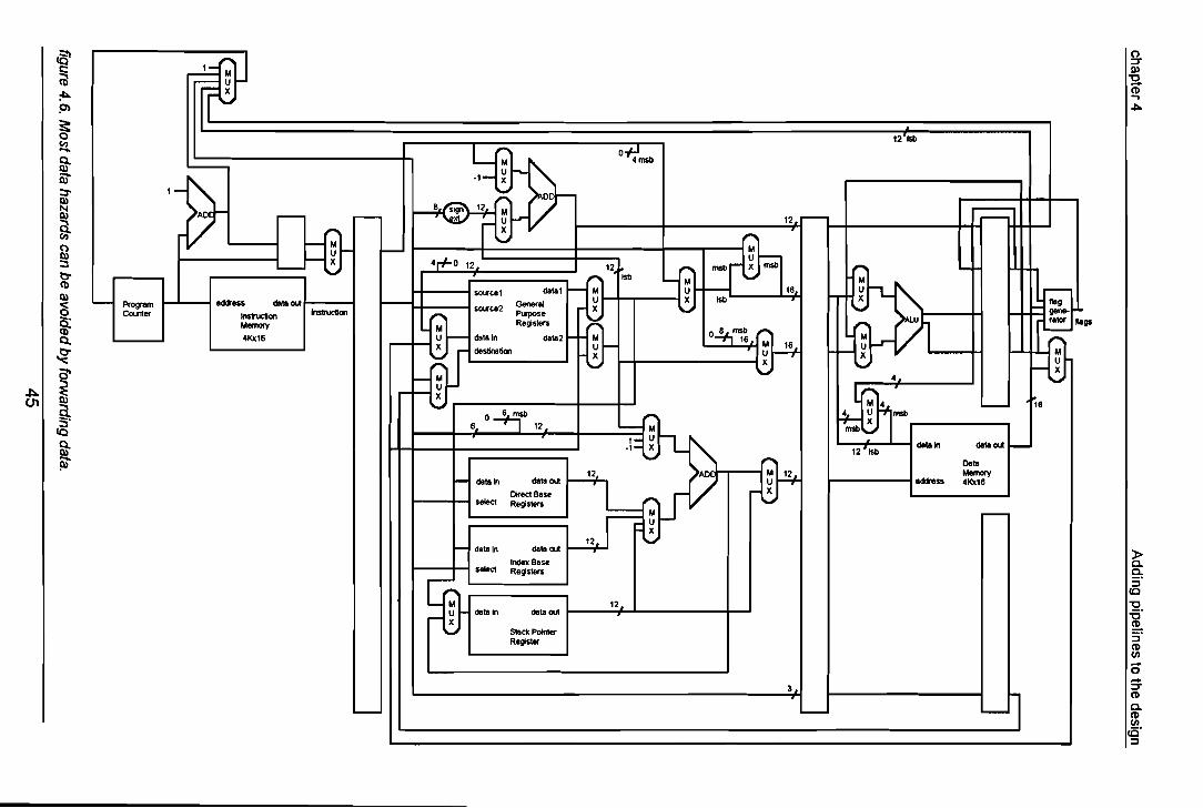
g.ll.l-g,CD...,~
»Co9:::JIC"0
~:;"CDVI-o-;;;rCDCoCDVI
cC'::J
gs
~ .12 Isb
~O+tmsb
'----1 ...... ~
'$- ~ 0
.-- .-- I ~c::> '~ 12 - .--
~1-n
.~u
~
~ .."-- x 4r+-O 12 12 ~
~ij-n ...v I
-'rf!sb M
SCU'ce1 U...... Program ed<tess deto out - Generel UI !sb X
~Cou1Ier lns1rucUon n sOLI'ce2 P~se X "'" V - gene- 10lns1nlctionMIITlOIY Registers ~
~JU
~~-1M O..!f,msb ....4Kx16 .--
~deto In deto2 - iM}- 16 M 16destinetion ~ I U~ ...
~~V IX V....4
-~-
V "'--- 16
o-4lsb r-6. 12. '---I M
I~U-1 X J 12 !sb
detoln deto out -V n Deto
- dete out
~"'0
~~MIITlOIY
detoln ed<tlss 4Kx16
Direct Bese ~X
select Registers V
-
- 12deto In dato out
Index Baseselec1 Registefs
ij- _. 12deto out
V Steek PointerRegister
3
-1- --
ca'§(Ij
~!=J)
~(Ij.....á}äl~OlNOla(Ij
0Ol::3trCIlOl;§g:Q.
~0'
.tl. ~0'1 a:i"IQ
á}!»

chapter 4 Adding pipelines ta the design
In case the Execute stage contains an instruction which alters the data for one of theGeneral Purpose Registers which is also used in the Decode stage for an indexedoperation, the pipeline has to be stalied until that data is available.
Now that the forwarding paths are implemented let's take a closer look at the loading ofan immediate value in one of the General Purpose Registers. If a 16-bit value must beloaded into one of the registers it must be done by two immediate move operations. Inthis example we will only concentrate on the execution of these two instructions.While the first instruction is decoded in the Decode stage the next one is fetched fromthe Read Only Memory. The Decode stage will prepare the data for the lower path of theALU. This data will contain the a-bit immediate value as the lower byte and a zeroes forthe higher byte. On the clock this data will be shifted to the Execute stage. In this stage itwill only pass the ALU without any arithmetic operations and is ready to be shifted to theWrite-back stage. But at the same time the next immediate move operation is a mhiinstruction. This instruction needs the lower a bits of the dataword which is still in theExecute stage. As there is no path back from that stage to the Decode stage astall willbe necessary. When the data from the first immediate move operation is shifted from theExecute stage to the Write-back stage the stall will be cancelled and the second moveoperation can proceed.This stall can be prevented by a simple change of the datapath. In figure 4.2 we movedthe multiplexors which were just in front of the ALU more to the front to save width of thepipeline registers. If we shift the two multiplexors that are responsible for the immediatemove operations back to the Execute stage the stall will be prevented. This is shown infigure 4.7.Now let us take a look again at the loading of a 16-bit immediate value in one of theGeneral Purpose Registers. The first move operation will do nothing in the Decodestage. The a-bit immediate value will be merely passed to the Execute stage. When itarrives in that state the a-bit immediate va/ue will be provided by a zeroes and on thedock shifted to the Write-back stage. In the meanwhile the second move operation wasdecoded in the Decode stage. As this stage doesn't do any data manipulations but onlypasses the immediate value to the Execute stage, no stall will be necessary. When thesecond move operation arrives at the Execute stage, the result of the first moveoperation is needed. As that data is now present in the Write-back stage it can beforwarded to the Execute stage. The complete 16-bit immediate value can now beformed and on the next dock be shifted to the Write-back stage.
4.3 Branch Hazards
Next to the data hazards are the branch hazards. An instruction must be fetched everyclock cyde to sustain the pipeline, yet in this design the decision about whether tobranch doesn't occur until the Write-back pipeline stage. One solution is to stall until thedecision whether to branch or not is taken. The drawback is that many times aconditional branch wil! decide against branching, and the work that would have beenaccomplished fetching and decoding the following instructions is exactly what will needto happen anyway.A common improvement over stalling when a branch instruction is in the pipeline is toassume that the branch will not be taken and so will continue execution down thesequential instruction stream. If the branch is taken, the instructions that are beingfetched and decoded must be discarded. Execution continues at the branch target.
46
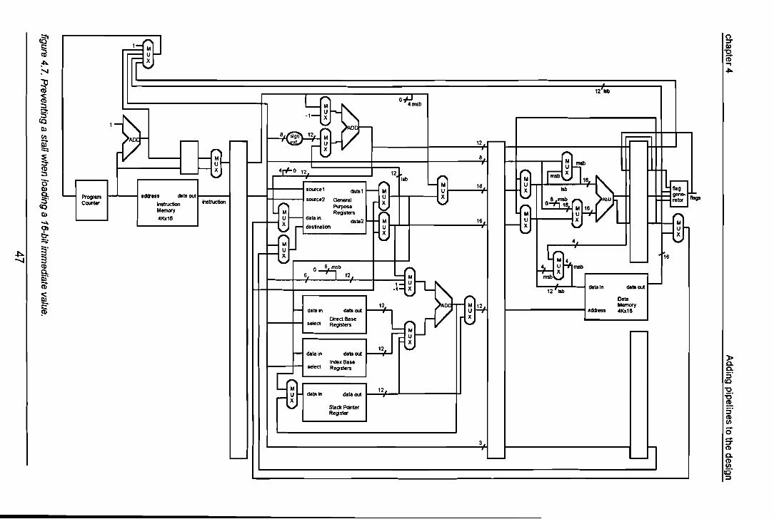
~0S'
10
~,"0~5'CDlil-o-=rCD0CD!a,
10:J
gs
~xJ-....
12 !sb
~~O+:msb-
'$- ~ 0
r-- .--
~ 12 .-- ""='"
~t 8f--
~X 4,+0 12 12 f"'lo'---- V
f"'loIsb
--1~ M16 U
sowee1datal~ M
~- Hx ~- Progllm a<lens. data out ---- SOU"ce2 Gener" U -.....
O!,c,msb ..... ALU - r.':naCOI01Ier lns1ruc1Ion lns1rUction
~P\rpose X
-f16 M 16
Mem<llY Registers ~ • U
~~4Kx16
r-- data In data2 ~ M 16~J
Xdestination U -.... ,..
X ~ ---I XV 4 V
-~-
16V -
o4-lSb -r;6 12
'=r data In _out~-1 X 12 !sb~ f"'lo Data
f- IL1'\0
~~~Mem<llY
data in data out adlt... 4Kx16
Direct Base
0select Registers V
~.--
.- data in data out
Irdex Baseselect Registers
f"'lo
~ ~t datal.12
data out
V Stack PointerRegister
3
--l-- -
e5'§(Ij
~:"l
~(Ij
~::3g:<0DlCl)
El::::::
~CD::3
0-Dl
~<0Dl.....0)
I
t:r:::;:
~§'
....... 3CD
~(j)
~c:~
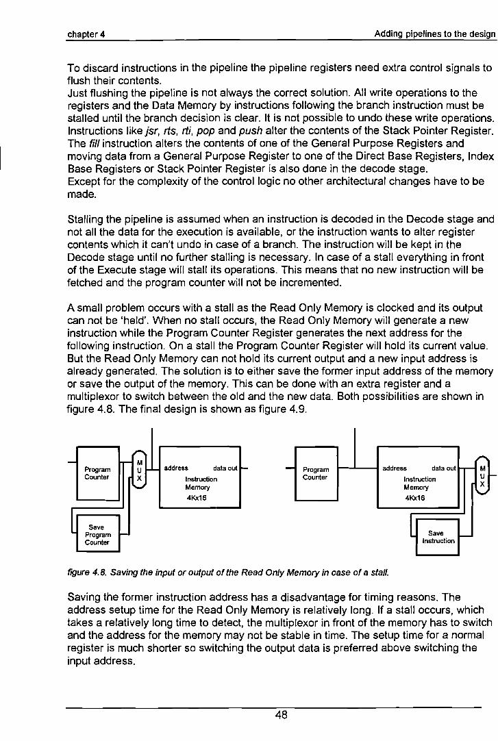
chapter 4 Adding pipelines to the design
To discard instructions in the pipeline the pipeline registers need extra control signals toflush their contents.Just flushing the pipeline is not always the correct solution. All write operations to theregisters and the Data Memory by instructions following the branch instruction must bestalled until the branch decision is clear. It is not possible to undo these write operations.Instructions Iike jsr, rts, rti, pop and push alter the contents of the Stack Pointer Register.The fill instruction alters the contents of one of the General Purpose Registers andmoving data from a General Purpose Register to one of the Direct Base Registers, IndexBase Registers or Stack Pointer Register is also done in the decode stage.Except for the complexity of the control logic no other architectural changes have to bemade.
Stalling the pipeline is assumed when an instruction is decoded in the Decode stage andnot all the data for the execution is available, or the instruction wants to alter registercontents which it can't undo in case of a branch. The instruction will be kept in theDecode stage until no further stalling is necessary. In case of astall everything in frontof the Execute stage will stall its operations. This means that no new instruction will befetched and the program counter will not be incremented.
A small problem occurs with a stall as the Read Only Memory is clocked and its outputcan not be 'held'. When no stall occurs, the Read Only Memory will generate a newinstruction while the Program Counter Register generates the next address for thefollowing instruction. On a sta11 the Program Counter Register will hold its current value.But the Read Only Memory can not hold its current output and a new input address isalready generated. The solution is to either save the former input address of the memoryor save the output of the memory. This can be done with an extra register and amultiplexor to switch between the old and the new data. Both possibilities are shown infigure 4.8. The final design is shown as figure 4.9.
,....- - M
Program U I- address data out ~Counter X Instruction
V Memory
4Kx16
l SaveProgram r-Counter
,....- Program address data out ..... M
Counter Instruction U r-
Memory X
4Kx16V
l Save r--Instruction
figure 4.8. Saving the input or output of the Read Only Memory in case of a stal/.
Saving the former instruction address has a disadvantage for timing reasons. Theaddress setup time for the Read Only Memory is relatively long. If astall occurs, whichtakes a relatively long time to detect, the multiplexor in front of the memory has to switchand the address for the memory may not be stabie in time. The setup time for a normalregister is much shorter so switching the output data is preferred above switching theinput address.
48

~C.:J
CC
"U
~S·(1)lil-o::T(1)
C.(1)lilcö·:J
gs
~12 !sb
~~O+tmsb-
'~>: DO
...-- ....--
~ 1~""'- r;:=-
1-(.')- '148
M msbI--I~
-
~~4r+- 0 12 12
~""'-- """~
Isb~
-<ij-datal I--t M1 16
~J !sb ~sOllce1 U -dabl OU! X .... :':na- ~m ed<tess
SOU"ce2Genere' ~J ~ 8 msb ,... ALU
Counter Instruclion -
~~PI6pose ~
....~
O~16.1 M 16Memory
''- ~ 1• U
~~4Kx16
Vdata in
deta2 M 16-1~J
Xr-- ....destneton
~J....
~ V ,......-t X
L.....-~ ..... 4. .....,....R~
~16
""---""" °41b
L(; ~~ msb""--- 6 12. msbV
.1~ ~ dablln dabl OU! I--12 !sb
V~ Deta
OrÄD rj ~Pt ed<tess
Memoryro- data In debl OU! 4Kx16
DireCl Bese ,.... XJseleCl Registers """M -U
X
t- dota In deblOU! 12 V
Index BeseseIeC1 Registers
"l-12
U data In data OU!r-I X
V Stock PoinlerRegister
3
""---~""--- ""---

chapter 4 Adding pipelines to the design
As mentioned before, stalling will prevent the program counter from being updated.If there is a branch taken the program counter must be updated so it can not be kept in a'hold' position as in case of a stal I. So all pipeline stages must continue their operations.In case a conditional branch instruction decides the branch to be taken it takes two cJockcycles to have the Fetch stage produce the next valid instruction for the Decode stage.As the Fetch stage continues all its operations it will still produce unwanted instructionsduring those two clock cycles. The Decode stage will receive instructions which were notmeant to be processed. This can be solved by filling the instruction register (the inputregister for the Decode stage) with two consecutive nop instructions. The nop instructiontells the processor to just do nothing in that particular stage the instruction is in. Fillingthe instruction register with nop instructions can be done by pre-setting the register.As the number of nop instructions to be inserted can differ for the several instructionswhich can cause a branch hazard, it is necessary to use a finite state machine controllerto control the loading of the nop instructions into the instruction register of the Decodestage. In the next chapter, which will describe the implementation of the microprocessor,this finite state machine will be explained in more detail.
The rts and rti instructions are very alike. The only difference is that the flags arerestored as weil in case of an rti instruction. Can the call for the interrupt routine be assimpIe as the call for a normal subroutine? The answer is yes. The only difference is thatthe call for the interrupt routine must also store the flag bits together with the returnaddress. In case of an interrupt a special instruction can be forced into the instructionregister so each pipe stage will know what to do. This will be called the int instruction.
In case of a jsr instruction it is obvious to save the return address of the next instructionfollowing the jsr instruction. An interrupt can also be considered as a jump to asubroutine (the interrupt routine). But what will the return address be? With 4instructions already in the pipeline it is not trivial what address that will beoIf there are no branch instructions in the pipeline the current program counter contentscan be saved as the return address.But in case there is a branch instruction in the pipeline, the pipeline needs to be drainedto decide if the branch needs to be taken. As soon as there is no branch instruction leftin the pipeline the instruction for the interrupt can be started.Instructions still in the pipeline can be finished normally if no branches are taken. Theaddress of the last instruction in the pipeline, incremented by one, must then be savedon the stack as the return address. If a branch must be taken the branch address mustbe saved on stack and the instructions following the branch instruction must bediscarded.If the pipeline contains an rts instruction when an interrupt occurs, the pipeline has to bedrained to resolve the return address from memory. This address can then be regardedas the return address.In the next chapter this will be explained in more detail.
50

chapter 5
5 Modelling and simulation.
Verification by simulation
Verifying the design can be done by simulation. There are several tools for simulatingdigital circuits. Each tooi has its own particular way of modelling the parts of the design.A hardware description language many people use today is VHDL. But VHDL is only adescription language. One needs a good compiler and an environment to check theresults. If a test is run and an error has been detected in the design, the simulationapplication must be stopped and the editor must be started to edit the design. Then thedesign must be recompiled, the simulator can be started again and another test can berun.This design has been modelled with IDaSS. IDaSS is an interactive design andsimulation environment for synchronous digital circuits. The advantage of IDaSS is thatthe models can be changed during the tests without quitting the simulator. Eachmodification is instantaneous. If a function is changed during a test, the output of thecorresponding function immediately adapts according to the change.This chapter will describe the way the design is implemented in IDaSS. The design isdivided into several smaller parts. These parts are the pipeline stages as have beendefined in chapter 4. They are shown again in figure 5.1. The pipeline stages Pre-fetchand Fetch will be combined into one part named Fetch.
12j~
::I: -"" ~U o.u U
::I: -.... ""',.~UJ U =>
LL. .... U •• UJ UJ UJUJ LL. >< ....0:= UJ~a.
"
figure 5.1. The design op the microprocessor devided into 5 stages.
As the datapaths for the microprocessor have a/ready been explained in chapter 4, thischapter wil! concentrate on the control logic for the parts of that datapath.
51

chapter 5 Verificatien by simulatien
Each pipeline stage is drawn in IDaSS with a layout corresponding to that of thedatapath layout as shown in figure 4.9. Appendix A contains the details of the IDaSSmodeis.
5.1 The microprocessor environment.
The microprocessor will be part of chip for data compression as is explained in chapter1. In our design the Data Memory was part of the datapath but it is actual an externalpart of the microprocessor. The microprocessor will be fiUed with input and outputbusses and signais, which will be called the addressbus and the databus, and thecontrol signals necessary to control these busses. This is shown at the right side offigure 5.2. The left side shows the interrupt input. As the Read Only Memory is also acomplex and large part of the microprocessor it is also drawn as an external part thoughit is part of the microprocessor.
r-ar-o
r-d"Ir-
up ahdi
intdo
figure 5.2. The microprocessor must communicate with the extemal Data Memory.
The read (rd) and write (wr) signals control the external databus. Mind however that theData Memory is not all Random Access Memory (RAM) but also contains memorymapped 110. Further more it contains separate busses for data to and for data from thatmemory.
The microprocessor is split into 4 parts as shown in figure 5.2. These parts represent thepipeline stages as defined in chapter 4.
~~ intad::: ~ad
ha ~ ~ ha Ja~ ~Ja
pa-.:l ""'ra dj. : :: dj. gs ~ ~nit::: ~ it at121 1'0 d2 :: ~d2ar ar~ ,...ar
Ma: ~ ..atetch decode eKecute writeback
idsd: :: sd
IW I-z..iw id: :id ie: ~ie
t~~l.~-Il.~ l[IH ~15L
~ MO
'U5Tr-- ~t -_IE :~ stlll~ r~"Or
::d I
:tl 1:1: :I:~I I I I
- I•r'li
figure 5.3. The microprocessor can be split into smaller parts.
52

chapter 5
5.2 The Fetch stage.
Verification by simulation
This stage actually includes the Pre-fetch stage and the fetch stage. This stage ho/dsthe Program Counter and the datapaths for generating the instructions. The Read OnlyMemory is part of this stage but is placed externally.This stage drawn in IDaSS is shown in figure 5.4.
l;n'Cb11
Figure 5.4. The fetch stage drawn in IDaSS.
The registers nia (next instruction address), pcs (program counter save), and si (saveinstruction) form the pipeline which separates the actual Pre-fetch stage from the actualFetch stage.
This stage needs control signals for the multiplexors. The multiplexor namux (nextaddress) is controlled by namuxc. The multiplexors amux (address) and imux(instruction) are controlled by intctrl which is a finite state machine controller that takescare of starting the interrupt call at the right time. The external interrupt signal will first besynchronised by a register. This register is called ireg. The register sic controls theregister si.
5.2.1 The logic block namuxc.
The multiplexor namux switches between the several busses which can generate the'next instruction address' for the program counter.
53

chapter 5 Verification by simulation
The controller namuxe contrals the multiplexor namux. This multiplexor must switchbetween 5 different inputs. In the IDaSS drawing the multiplexor only has 4 inputs butone of the 5 inputs is a constant value. This value is generated internally.These 5 values are coded with 3 bits as is shown in table 5.1.
sela4.<>·\··56Ià1<··< 56Ia3</·······
.••••••••••••••••••••••••~.~.:.~~ •••••••••••••.•.•..•...
a4··a1········83··
. . ···2....••....> ···a ......••.... ·1················0·0·1hvaue
load incremented program counter/load jump addresS··..<load return address\)load branch addres5\\load interru t startadcl~é5kbö1h
table 5.1. The control signals for namux.
The control signal C is formed by the functions as shown in figure 5.5. The signal id isthe instruction which is active in the Decode stage. The signal iw is the instruction whichis active in the Write-back stage. The signal br is 1 in case a conditional branchinstruction in the Write-back stage decides that a branch must be taken.
-----------------v----------------------"~mp is 1in case id is a jsr or jmp instruction"~mp:= ((id from: 13 to: 15) = %100)."_ret is 1 if iw is a rts or rti instruction"_ret := ((iw trom: 13 to: 15) = %111) /\ (iw at: 5)/\ ((iwat: 3)not)."_int is 1 in case id is an interrupt caU"_int := ((id trom: 13 to: 15) = %111) /\ ((id trom: 3 to: 5)=%010).
". ".-'. .
"note:execution ot rts or rti inserts 4 nops in the decode stage.""So ~mp and _ret can not be active at the same time""_int can not be active together with a branch, ~mp or _rts"
c := _int,(br V_ret),(br V~mp)_________________" _
figure 5.5. The model for namuxc.
5.2.2 The logie bloeks amux and imux.
The Logic block amux is an ordinary multiplexor. It switches between the two inputs niaand pes as is shown in table 5.2. Switching is done by the finite state machine controllerintetrl.
table 5.2. The functions of multiplexor amux.
The logic block imux is also a multiplexor. The control however is somewhat morecomplex. The finite state machine controller intetrl switches between three functions.One of these functions is the generating of the nop instruction. Another is the generatingof the int instruction.
54
chapter 5 Verification by simulation
The third function is named normal and is an ordinary multiplexor function whichswitches between the two inputs rom and si. Switching between these two inputs iscontrolled by the input signal sic. This is shown in table 5.3.
~~:~: .~~~~~ i>frbminput róm< ..frbrninüt si ....
table 5.3. The outputs of logie bloek imux.
5.2.3 The finite state machine controller intctrl.
This part of the microprocessor is probably the most complex part. In case of an interruptit takes care of saving the right return address on the stack and activates the interruptroutine at the proper time.This microprocessor does not allow nested interrupts. If an interrupt routine is started theinterrupt signaI will be masked until the interrupt routine has finished.The interrupt routine would poll the various possible interrupt sources to see which eventcaused i1. Reading the status register of the interrupt source must deactivate theexternal interrupt signa!. After finishing the interrupt routine a new interrupt routine canbe started if the external interrupt signal is active again.
As we have seen in paragraph 4.1 (figure 4.5) the flags must come from the flag registerof the Write-back stage. Between the interrupt instruction and the last instruction of theinterrupted program, a nop instruction must be inserted to assure that the proper flagsare saved on the stack.
The most simple case for starting the interrupt routine is when there are no addressaltering instructions in the pipeline (conditional branch instructions, rii, ris, jmp andjsr)and the stall signal (sf) is not active. As the finite state machine is implemented as aMoore-machine during the first clock cycle when the synchronised interrupt signal isactive, the interrupt signal wil! only prepare the finite state machine to jump to anotherstate. During that clock cycle the microprocessor will continue its uninterruptedoperation. On the next clock the instruction which was prepared by the Fetch stage willbe clocked into the instruction register of the Decode stage. At the same time the pcs(program counter save) register will hold the address of the next instruction that isfetched from the Read Only Memory. So if we hold that address, discard the instructionthat resides at that address (which at that time comes from the instruction memory or thesi register) and present a nop and an int instruction sequentially the interrupt routine callcan be started. Together with the interrupt instruction the return address coming from thepcs register wiJl be passed to be saved on stack.
But what happens if there are address altering instructions in the pipeline or astalloccurs at the time the internal interrupt signaI is activated? Each of these possibilities wilbe examined.
55

chapter 5 Verification by simulation
1. As expJained above when no stalIs occur and/or there are no address alteringinstructions present in the pipeline the pcs register must be held and a nopinstruction must be inserted. Then the int instruction will be inserted together with thecontents of the pcs register which is the return address that has to be saved on thestack.
2. If astall occurs the interrupt has to be stalled as weil until the stall is lifted. If nofurther address altering instructions are present in the pipeline the interrupt call canbe initiated as in situation 1.
3. If the branch signal (br) is active a conditional branch must be taken. All instructionsin the pipeline are discarded and need no further investigation. The address to bebranched to will be present in the pcs register after 2 dock cycles. That addressmust be saved as the return address of the interrupt routine. During those two clockcycles nop instructions can be inserted. This is not really necessary because thecontroller of the Decode stage will reset the instruction register during those clockcycles as we will see later when the function of that controller is explained.
4. In case there are conditional branch instructions present in the Decode stage and/orthe execute stage, the pipeline has to be drained until the last conditional branchinstruction is present at the Write-back stage. During that time the pcs register mustkeep its contents. If the branch must be taken situation 3 occurs again. Jf no branchoccurs situation 1 will arise.
5. If the Write-back stage contains a jmp or jsr instruction the Fetch stage has alreadyfetched the new instruction from the Instruction Memory. The pcs register will holdthe address of the new instruction. The Decode stage and Execute stage will containnop instructions due to the presence of the jmp or jsr instruction in the Write-backstage so it is not necessary to check for the instructions in the rest of the pipeline.Situation 1 can be applied here again.
6. If the Write-Back stage contains an rts instruction the address coming from the DataMemory must be used as the return address for the interrupt routine. Two nops haveto be inserted before the address is present in the pcs register. Then the intinstruction can be inserted. The Decode stage and Execute stage will contain nopinstructions due to the presence of the rts instruction in the Write-back stage.
7. If the Execute stage contains an rts instruction situation 6 occurs again except thatan extra nop must be inserted before the int instruction can be inserted. The Decodestage will contain a nop instruction due to the presence of the rts instruction in theExecute stage.
8. If the Execute stage contains a jmp instruction (and the branch signal is not active)or jsr instruction the Program Counter Register is already holding the address of thenext program instruction. While inserting a nop instruction the pcs register must beJoaded with the contents of the Program Counter Register after which the intinstruction can be inserted in the next dock cycle.
56

chapter 5 Verificatien by simulatien
9. If the Decode stage contains an rts instruction it is possible that the Execute stagecontains a conditional branch instruction. This will however result in astall while theconditional branch instruction moves on to the Write-back stage. If the conditiondecides against branching the rts instruction can proceed its execution. After oneclock cycle the rts instruction has moved on to the Execute stage after whichsituation 7 occurs again.
10. If the Decode stage contains a jsr instruction it is possible that the Execute stagecontains a conditional branch instruction. This will however result in a sta 11 while theconditional branch instruction moves on to the Write-back stage. If the conditiondecides against branching the jsr instruction can proceed its execution. After oneclock cycle the jsr instruction has moved on to the Execute stage after whichsituation 8 occurs again.
11. If the Decode stage contains a jmp instruction it is possible that the Execute stagecontains a conditional branch instruction. This wil! not result in a stal!! The jmpinstruction will proceed its normal behaviour and can be overruled if the conditiondecides to branch when arrived at the Write-back stage. In that case situation 3occurs again. If the condition decides against branching the jump address hasalready arrived at the Program Counter Register. The pcs register must load thejump address on the next clock. This jump address will be saved as the returnaddress.
All these situations must be controlled by the finite state machine controller intctrl. Thestate description diagram is presented as figure 5.6. For each of the states the functionsof the two multiplexors imux and amux and the register pcs are shown in table 5.4. TheIDaSS model is to large to show here. It can be found in Appendix A.
State 11 is entered when the int instruction has been inserted into the pipeline. It will notcontinue to state 1 until the rti instruction has arrived at the Write-back stage. Thisprevents nesting of interrupt routines.
If there are no address altering instructions in the Decode stage, Execute stage and/orWrite-back stage the finite state machine will proceed to state 9 on an interrupt. Whenarrived at that state the Decode stage will have received a new instruction which stillneeds to be processed. This instruction can again be an address altering instruction. Ifnot, the finite state machine will proceed to state 3 where it will insert the instruction intto start the interrupt routine.
57

chapter 5 Verificatien by simulatien
stall-br-iebr-idjmp +
stall-br-idjsr +
stall-br
br
stall-br-(idbr + iebr-idjmp)1------......;...---+17
stall-br-iebr-idjmp
stall
stall-br-idrts5
int-stall-br-idbr +int-stall-br-iebr-idjmp
int-stall-br +
int-staij-br-iwrts +
int-stall-br-idjsr +
int-Staii-br-idjmp-iebr
stall-idbr-idrts-idjmp-idjsr
figure 5.6. The state transition diagram of intetrl.
niapcs ....pcs.·pcspCspcspcspcspCS
pCS
nia
laadIbadlaadhaldlaadlaadhOlçthald ..
hord·IOadlaad
table 5.4. The funetions of amux, imux and pes in eaeh state of intetrl.
58

chapter 5
5.3 The Decode stage.
Verification by simulation
The Decode stage holds all the Data Registers. These are the 8 General PurposeRegisters (GPR), the 16 Index Base Registers (IBR), the 2 Direct Base Registers (DBR)and the Staek Pointer Register (SPR). As the latter 3 type of registers are never used atthe same time they ean be elustered into one big registerfile of 19 registers. They aremodelled as the logie bloek regs. The address selection of these registers is done by alogie bloek named regsel. The pipeline register is formed by the registers adreg andidreg. The instruetion addresses are passed by adreg. The instruetions that aregenerated by the Feteh stage are eloeked into the instruetion register idreg whieh iscontrolled by a finite state machine controller idetrl.The Decode stage drawn in IDaSS is shown in figure 5.7. At the top of the drawing are 4logie bloeks whieh control this stage. The logie bloek deeeirl contrals most parts of thisstage, sueh as the multiplexors. The logie bloek wbetrl generates the write signal for theGeneral Purpose Registers. The logie bloek fbetrl controls the feedback multiplexors ofthis stage. The logie bloek stal/ generates the stall signa!.
Isel
hr " hr sel - ~sel ;S ~.iW ~ lrl iW ;;1-• i. ~~cctZ" ...betrl betrC lel " ld " id
ie stall 0
r-~.d sC --0~: 1!- -
~
I ------,I I iel
-----J I I I
II
lI I I 1 I§B-~i ~ oEI- :5: ad
adreg I aeleler
lI>li'? " i d out ... ba
B f-- I "dZ 'oP
fB ,--,d ~~ od ~ • • [--§]~ e dJ...u>c
~ id slill lil sJ.
~If-- dl rilf--~ cU 01 a :5: elJ. l'I\'l
gprsel elZ mf--I:J dZB-l!Ii ollf- s~'-- In sZ
idregCh..u>c
EJoZ
...!REGCPR ~EJ"o ...
" iel ~eles ..u)(
l!Iao'oP
lil iw de~-I;Ides
{Sdin JRAi
~fl ~ lil• 1.. 0
BdinMux
I1TF~"0I" ao mi
B 'EEI ~2 aeldrlil-EJ" lel
::iel ~aeldrsel
spChlll:rR!JIi. ~ IS - l!I s.l o· .....go
""'" ~regs
~ oril - ~datr- IiJspCh
regMU>CJRAi
ISdJ. r()i
figure 5.7. The IDaSS drawing of the Decade stage.
59

chapter 5
5.3.1 The legie bleek decctrl.
Verification by simulation
This block is actually the instruction decoder. It switches the functions of several logicblocks. Those logic blocks are shown in tables 5.5 to 5.10.
table 5.5. The functions ofmultiplexor d1mux.
select bits 0..2 of iw as inputsèlect bitsS..8 of id as in ut
table 5.6. The functions of multiplexor desmux.
table 5.7. The functions ofmultiplexor regmux.
Multiplexor dinmux is somewhat more complex. It has 3 input busses to be switched towhich means that it needs 2 controllines. One of those control lines comes from thecontroller deeetr/. It switches between the output of the adder (at the top) in case of a ti"instruction and the output of the Write-back stage. The latter however can be the outputof the ALU or the output of the Data Memory. An extra control line is needed to selectbetween those two inputs. This controlline is not fitted as one signal but as theinstruction bus iw. A function internalof dinmux determines which input must beselected. This internal signal will be called am (ALU or memory). If it is zero, data fromthe ALU will be selected. If it is one, data from the Data Memory is selected.
functien contraI value am value·alumem ..
......... ...
SadderS<
o
1
o1
select input aoselect input moselect in ut fl
table 5.8. The functions of multiplexor dinmux.
The logic block named adder at the top of figure 5.10 contains the adder whichcalculates the branch address. The branch address is calculated by adding thedisplacement to the next instruction address. The displacement is formed by bits 4 to 11of the instruction word id extended to 12 bits. This adder is also used to decrement thecontents of one of the General Purpose Registers in case of a ti" instruction. Thecontroller deeetrl will switch between those two functions.
ut d2.
table 5.9. The functions of logic block adder.
60
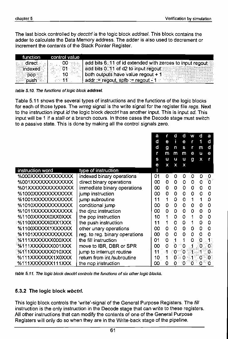
chapter 5 Verification by simulation
The last block controlled by decctrl is the logic block addrsel. This block contains theadder to calculate the Data Memory address. The adder is also used to decrement orincrement the contents of the Stack Pointer Register.
).9ireS.t / ••• ··ihdexéd .•.••••...
<pop··..... üsh<
table 5.10. The funetions of logie bloek addrse/.
Table 5.11 shows the several types of instructions and the functions of the logic blocksfor each of those types. The wrreg signal is the write signal for the register file regs. Nextto the instruction input id the logic block decctrl has another input. This is input sd. Thisinput will be 1 if a stall or a branch occurs. In those cases the Decode stage must switchto a passive state. This is done by making all the control signals zero.
a r d d w d ad e i e r 1 dd g n s r m dr m m m e u es u u u g x re x x x
instruction word t e of instruction I%OOOXXXXXXXXXXXXX indexed binary operations 01 0 0 0 .0 0 0%001 XXXXXXXXXXXXX direct binary operations 00 0 0 0 0 0 0%01 XXXXXXXXXXXXXX immediate binary operations 00 0 0 0 0 0 0%1OOOXXXXXXXXXXXX jump instruction 00 0 0 0 0 0 0%1001 XXXXXXXXXXXX jump subroutine 11 1 0 0 1 1 0%101 OXXXXXXXXXXXX conditional jump 00 0 0 0 0 0 0%1011 XXXXXXXXXXXX the djnz instruction 00 0 0 0 0 0 0%11 OOXXXXXOXXOXXX the pop instruction 10 1 0 0 1 0 0%1100XXX)(XOXX1XXX ..... the push instruction 11 1 0 0 1 0 0%·11 00XXXXX1 XXXXXX other unary operations 00 0 0 0 0 0 0
.. %1101)()()()()()()() reg. to reg. binary operations 00 0 0 0 0 0 0.%111 xx>oo<xxOOOXXX the fill instruction 01 0 .1 1 0 0 ...... 1%1J1XX>OO<XX001XXX move to IBR, DBR or SPR 00 0 0 0 1 .......• 0 0··
%111 XXXXXXX01 OXXX jump to interrupt routine 11 1 ···0······ 0 «1 ····1 ··.....•.. 0.....%111 XXXXXXX1 XOXXX return from il1t.1subroutine 10 1 0 0 >1 ·0 g%111 XXXXXXX111 XXX the no ihstruction 00 0 0 0 0 0
table 5.11. The logie bloek deeetrl controls the funetions of six other logie bloeks.
5.3.2 The logie bloek wbctrl.
This logic block contrals the 'write'-signal of the General Purpose Registers. The fil!instruction is the only instruction in the Decode stage that can write to these registers.All other instructions that can modify the contents of one of the General PurposeRegisters will only do so when they are in the Write-back stage of the pipeline.
61

chapter 5 Verification by simulation
These instructions are:
• The binary operation mov, which moves data from the Data Memory to a GeneralPurpose Register. This can be either an indexed or direct binary operation.
• Any other binary operation except for the emp operation.• All unary operations except for the push operation.• The djnz instruction.
These conditions are modelled with IDaSS and shown in figure 5.8.
---'""''''"--'''"------v--------------------"writebacktoaGPR"
~f.llid:Ç«idirom:13to:15) = 1)10111) 1\ «idfro~:3 to: 5) = %OOO).i'thefill instruction"_binwriw := «(iw from: 14 to: 15) = %00) 1\ «iwat: 3) = %0» V "direct or indexed mov opèration"
««iw from: 14 to: 15) = %01) V«iw from: 12 to: 15) = %1101» 1\ "other binary operations"«iw from: 3 to: 5) -= %111». "except cmp"
_unwriw:= «iw from: 12 to: 15) = %1100) 1\ «(iw from: 3 to: 6) = %0001) not). "all unary except push"_djnziw := «iw from: 12 to: 15) = %1011). ''the djnz instruction"
wr := _fillid V_binwriw V_unwriw V_djnziw__________________A _
figure 5.8. The IDaSS model of wbctrl.
5.3.3 The logie bloek fbetrl.
This logic block controls the two feed-back multiplexors of the Decode stage. The logicblock fbmux contains those multiplexors and table 5.12 shows the coding of the controlsignais. Each of the two multiplexors switches between the output of the GeneralPurpose Register, the output of the ALU or the output of the Data Memory. The outputsare named 01 and 02.
function control value out ut 01 out ut 02normal ...fbd1alu
fbd1mémfbd2àlu .
fbd2merl'l. fbbothalu
/fbbothmem
XOO001101010110 ...011111
data from GPRdata from ALUdata from Data Memorydata from GPRdata from GPRdata from ALUdatafrom Data Memo
data from GPRdata from GPRdata from GPRdata from ALUdata from Data Memory ...•...data from ALUdata from Data Memo
table 5.12. The coding of the control signal C for logic block fbmux.
Of course these feed-backs will only be necessary in case the Write-back stage containsdata to be written in one of the General Purpose Registers and the instruction currentlyin the Decode stage needing that data. In case of a feed-back the data comes fromeither the ALU or from the Data Memory. They can not produce their data at the sametime.The instructions at the Write-back stage that can write data to one of the GeneralPurpose Registers are already discussed at section 5.3.2. Figure 5.9 shows the IDaSSmodel of fbefrl.
62

chapter 5 Verification by simulation
c:= __mêrri./ . / .. . .. .«(iw from:O to: 2) = (id from: 6 to: 8» 1\ _RGWiw) "fb02"
--..----.-~~~~~·-·v----·-··-----····----"feedbàêkcol1trol forthe decode stage""fb01 = (iws1 = ids1) and RGWiw : feedback data of source1" ."fb02= (iws1= ids2) and RGWiw : feedback data of source2"< ....
")~~~is1ig6~~e ofarnemory to register move andincase of a pop"_mem:=«(iw from:14 to: 15) = %00) 1\ ((iwfrom: 3 to: 5) = %000» .
< «(iwfrom: 12 to: 15)= %1100) 1\ ((iw from: 3 to: 6r= %0000».<
";;it~6~gktbthpR"· ......•.. . ... .... /,X\l;~[2{<2{.,,2{,,)1"'birïwriw :=«((iw from: 14 to: 15) = %00) 1\ ((iwat: 3) = %0» V "direct and indl~xel~binar m
i «(iwfrom: 14to:15) = %01) 1\ ((iw from:3 to: 5)-=%111» V "imm) «((iwfrom: 12 to: 15) = %1101) 1\ ((iwfrom: 3 to: 5)~=%111»."reg-reg biniarYop~; e)l:~~)r6Imï
2ûnwriw:=((iwfrom: 12 to: 15) = %1100) 1\ «(iw(rom: 3 to:6) = %0001) not).~djnziw :=((iwfrom: 12 to:15)=%1011)."thedjl1zinstruction" ...••...
"__~~VVi;iSfif the instruction iM i;w~tes b:Ck to on~ ofthe GPRs"_RGWiw := _binwriw V_unwriw V_djnziw..
..:,«(iwfrom: 0 to: 2) = (id from: 0 to: 2» 1\ _RGWiw) "fb01"
• • ...._A ••~~ _
figure 5.9. The IDaSS model of fbetrl.
5.3.4 The logie bloek stalI.
This block is the most complex part of the Decode stage. It will produce the stall signalsfor the microprocessor. In case an instruction arrives at the Decode stage that can notstart its operation because it needs data that will not be available until the next clockcycle, it will have to stall the fetching of the next instruction. The instruction in theDecode stage must stay passive until it can start its operation. The instructions at theExecute and Write-back stages must continue their operations. There are severalreasons why astall can occur:
• As the Data Memory is a relatively slow device, the data from that memory can not befed-back to the Execute stage. This means that any instruction that loads data fromthe Data Memory and that is immediately followed by an instruction needing that datamust be stalied.
• The ti" instruction will write back data to one of the General Purpose Registers oneach clock cycle. It must stall its operation if there are instructions in the Executeand/or Decode stage that want to write back their results to one of the GeneralPurpose Registers even if different registers are used.
• If there is a mov instruction to one of the Index Base Registers, Direct Base Registersor to the Stack Pointer Register and the data to be written to that particular register isgoing to be produced by the preceding instruction the mov instruction has to bestalled until that data is produced by the Write-back stage one clock cycle later.
• An indexed operation needs the contents of one of the General Purpose registers forthe calculation of the memory address. If the contents of that particular register isgoing to be changed by the instruction preceding the indexed operation then a stall isinevitable.
63
chapter 5 Verification by simulation
• If there is a conditional instruction in the Write-back stage and the condition decidesfor branching all other instructions in the pipeline have to be flushed. Therefore noalterations to register contents may be made by the instructions directly following theconditional branch instruction. Instructions that alter register contents in the decodestage are: fil! (General Purpose Register), pop, push, jsr, rts and rti (Stack PointerRegister) and moves to one of the Direct Base Registers, Index Base registers orStack Pointer Registers.
There are different conditions for stalling the Decode stage and for stalling the Fetchstage. Both pipeline stages will have to stall on the conditions mentioned above. But theFetch stage also has to stall when the Decode stage contains the fill instruction until thecontents of the selected General Purpose Register has been decremented to zero.
On a stall all control signals of the Decode and Fetch stage will get a passive valuewhich results in a situation where no modifications are being made. For the Fetch stageit will amongst other things result in not incrementing the program counter. The stallsignal std will force the instruction register of the Execute stage to load a nop instructionduring the next clock cycle.Flushing the Decode stage in case of a branch will have the same effect for the controlsignals as in case of a stal I. So these signals can be combined into one signaI. TheFetch stage on the other hand must continue its operation in case of a branch and maynot respond to the stall signal when the branch signal is active.As the IDaSS model is too long to print here only a summary of the IDaSS model will begiven here as figure 5.10. The complete model can be found in Appendix A.
----------------------v----------------------"stf is the stall signaI for the Fetch stage""std is the stall signal for the Decode stage"
"jd is the instruction in the Decode stage""ie is the instruction in the Execute stage"
. . ..
"~..idmemrd is fwhen data will go from memory to a register""_samereg1 is 1 if the write-back registerof ie is also used in id as register1""_sàrnèreg2 is 1if the write-back register of ie is also used in id as register2""_regop is1in case an instruction uses oneof the General Purpose Registers""_regwrieis1 if ie will write-back to a register""_règwdwis1if iw will write-back to a register""_indid··isfifid Tsànindexed opëration"··" fillidiSfifid is a fill instruction" ."=popidisJlf iëris àpop instructio""II-f5Ûshid Îsfif idlsa pLJsh instruction"./ .."_retLJrJ1Idis1ifidis an·rti or rts instrudióri""jsrid is fif idis a jump subroutine instrudion""_movridis 1 if id is ä move to IBRIDBRISPR instruction""_co"dbfieis 1 ifTéis a conditional bränc:hinstruction""_stdtoreuse thé equälion of std for stf'
64

chapter 5
figure 5. 10. Part of the IDaSS model of stalI.
Verificatien by simulatien
5.3.5 The finite state machine controller idctrl.
The last block of the Decode stage that hasn't got any attention so far is the finite statemachine controller idctrl. This finite state machine contrals the functions of the instructionregister idreg. This register can be hold, preset or loaded. In case of astall it must behold.In case of some instructions nop instructions need to be inserted to guarantee properoperation of the pipeline. For instance in case a jmp instruction is decoded in theDecode stage it takes two clock cycles to select the new program address and fetch thenew instruction from the Instruction Memory. As the Fetch stage can not flush anyinstructions the instruction register id will have to do that. During the two clock cyclesafter the jmp instruction has left the decode stage the instruction register id must bepreset to produce the nop instruction. The two instructions produced by the Fetch stagewill automatically be rejected.The instructions that need this feature are the instructions jmp, jsr, ris, int and rii. Theinstructions ris and rii need four nop instructions inserted. The other three instructionsneed only two nop instructions inserted. Two nop instructions need also be inserted incase a conditional branch is taken.If there is a jmp instruction in the Decode stage and a conditional branch instruction inthe Execute stage the finite state machine controller will start producing two sequentialnop instructions. When the conditional branch instruction arrives at the Write-ba.ck stageone clock cycle later and the condition decides that the branch must be taken thepipeline must be flushed and the jmp instruction must be discarded. The finite statemachine controller has only produced one ,nop instruction at that time. It must bestopped generating the second nop instruction but on the other hand for the branch to betaken it must again start to generate two sequentiaI nop instructions.In case the function of the instruction register must be changed it must be done beforethe next clock. Therefore this finite state machine must be implemented as a Mealymachine.The state transition diagram is shown in figure 5.11. With each transition the function forthe instruction register idreg is given.
65

chapter 5
tir-sf/hold
br/reset +--br·sf-(jmp+jsr+int)/reset
figure 5. 11. The state transition diagram of idctrl.
5.4 The Execute stage.
br-sf-rts-rti·jmp-jsr-intlload
br/reset
Verificatien by simulatier
-/load
The Exeeute stage holds the ALU and it prepares the data for the Data Memory. As theData Memory is a synehronous device it will be part of the pipeline register between theExeeute stage and the Write-baek stage. The parts of the Exeeute stage are controlledby two logie bloeks. The feed-baek multiplexor is controlled by fbetr!. The other parts arecontrolled by exetr!. The latter also generates the read and write signals for the DataMemory. The IDaSS drawing of the Exeeute stage is shown in figure 5.12.
5.4.1 The logic block tbctrI.
The logie bloek fbetr! contrals the two feed-baek multiplexors whieh are modelled as logiebloek fbmux. As the Data Memory is a relatively slow device it will not be fed-baek to theExeeute stage. The only data that ean be fed-baek is the data from the ALU once it haspassed the pipeline register at the output of the ALU. If the instruetion in the Exeeutestage needs the data whieh is going to be written back by the Write-baek stage it simplyswitches the multiplexors to that data.
66
chapter 5 Verificatien by simulatien
I br~ ~br af' - I.r.af' Ird aol t'"'..r~
I i .. ...I Zi .. o~ r- exctrl rd Ii f'bc trI 19 - ctrl:- Bie rnp - C Ie l'iVi: I.r. ..r IOP ï
~ie II I ï'
~~~.;j EJr sdi I I I
lfI lfIlid*- l=Ji~ 0-
_ _ c c• lMM ;E: al uJ. grsM :: I.r. gS Iiereg ... I"'" al uJ. ::
FJRE(
iMMMUX ALUI dJ. *- ~c~l:Ji o~IL-S dJ. Co J. : ~ dJ.dJ. reg
l5E( f'bMUX alu2 :: ;::: alu2 resul t :: ~ar II *- W- S d2 02- ~d2
d2 .i 0 - tOP roPl:Jd2reg I!l -Sf'b lM..IRE< OP
I
I ao ~ ';" dJ. ~...
If'l~f'IMux ... I,., Mi I0
::: f'l - FOP
B-f~._~---------------------iEJ
figure 5.12. The IDaSS drawing ofthe Exeeute stage.
The two multiplexor outputs are 01 and 02. They can be switched between data from theDecode stage and the feed-back data. Table 5.12 shows the control signals for the logicblock fbmux.
function contral value out ut 01 out ut 02normalfbdata1
·fbdáta2fbboth
00011011
data from input d1data from ALU feed-backdata from input d1data from ALU feed-back
data from input d2data from input d2data from ALU feed-bêckdata from ALU feed-báck
table 5. 12. The eoding of the control signal C of the logie bloek fbmux.
The simplest way to detect if a feed-back is necessary is to check whether the instructionin the Write-back stage is going to write back to one of the General Purpose Registersand then check if that specific register is also used by the instruction in the Executestage. The simplest way is to check if the bits with which the registers of the GeneralPurpose Registers are selected (bits 0..2 and bits 6..8) have a match with the write-backselection address of the instruction in the Write-back stage (bits O..2) independent of theinstruction in the Execute stage.There is one exception to this solution. No feed-back may be applied if the instruction inthe Execute stage is a jsr or int instruction. The data from the Decode stage must passoutput 01 the multiplexor as it must be written to the Data Memory. This data is thereturn address which must be written on the stack.
67

chapter 5
The IDaSS model of fbetrl is shown in figure 5.13.
Verification by simulation
--------------v-----------~~--------
"feedback control""fbo1 = (iws1 = ies1) and RGWiw and (ie <> jsr) and (ie <> int)""fbo2 = (iws1 = ies2) and RGWiw" ..
"vIriteb~~lc;toaGPR O~lyjromthe ALU()utput" .....•...... ....•...... .«._binwriw := «(iw from: 14 to: 15) = %01) 1\ «iw from:3 to: 5)"'=%111» V "imm binary<.(Ww from: 12 to: 15) = %1101) 1\ «iw from: 3 to: 5)-=%111». "reg-reg binary ops
_unwriw:= «iw from: 12 to: 15) = %1100) 1\ ((iw from: 3 to: 6):"'= %0001). "all unaryops _..__...:. _djntiw :=((iw from: 12 to: 15)=%1011). ''the djnz instruction"
;~katVi~~~1if the instruction in iw writes its ALU output back to one ofthe GPRs"_RGWiw:= _binwriw V_unwriw V_djnziw........ ..::::-::-.... ::...:.:". .
~trl:~«((i~ ir~m: 0 to: 2) = (ie from: 6 to: 8» 1\ _RGWiw) "fbo2",«(iwfrom: 0 to: 2) = (ie from: 0 to: 2» I\_RGWiw 1\) "fbo1"«ie from: 12 to: 15) -= %1001) 1\) "not in case of a jsr instruction"««ie from: 13 to: 15) = %111) 1\ «ie from: 3 to: 5) = %010» not» "not in case of an int instruction"
------------------,,----------------------figure 5.13. The IDaSS model of logic block tbctrI.
5.4.2 The logie bloek exctrl.
This bloek is aetually the instruetion decoder. It switches the funetions of the logie bloeksflmux, immmux and ALU and generates the control signals for the Data Memory. Thelogie bloeks are shown in tables 5.13 to 5.15.
The logie bloek flmux always passes the lower 12 bits of input d1. The upper 4 bits eaneome from input d1 or from input fI.
table 5.13. The functions of muftiplexor f1mux.
The logie bloek immmux is the multiplexor that switches between normal data feedthrough or data modifieations eoneerning immediate data operations. This logie bloekeontains two multiplexors that are switehed by two control signais. These signals areeoded as shown in table 5.14.
funetion control valueimmlowirnmhigh
..opimrn() nonnal
00011011
alu2 its lower part is imm value extended with zeroesalu1 its upper part is imm value, lower part that Of d1alu1 gets value of d1, alu2 same as immlowalu1 ets value of d1, alu2 ëts value of d2
table 5.14. The coding ofthe control signal C of logic block immmux.
68
chapter 5 Verification by simulation
The logic block ALU can perform 16 different arithmetic operations. These operationsare already discussed in section 2. Some adaptations have been made to the encodingof the unary operations. These are discussed in section 2.8. Table 5.15 shows theencoding of the functions the ALV must be able to perform.
sel2sel3cplsetdecshrshl8shr8
0000··Ö001001000110100 ...
. ..
. 01010110011110001001101010111100110111101111
the output gets the value of input alu2 .•.théoUtpufgètsthe váluéof input àlu1 .alu1+ alü?> ...•••...
älü1 -~.lu2 ..>/.. ... ..•.... ···jtlhlnlodt{> >n» }a bitwiseandópèration on hea bitwise or operation oh botha bitwisèxor operation' on boththe value of alu1 compared to that ofselect the second nibble of alu1 (bits 4..7)select the third nibble of alu1 (bits 8.. 12, note: 5 bits)a bitwise invert of the bits of alu1the output bits all get value 1alu1 - 1shift all bits of alu1 right one bit, a zero is shifted inshift all bits of alu1 left 8 bits, zeroes are shifted inshift all bits of alu1 ri ht 8 bits, zeroes are shifted in
table 5.15. The coding of control signal C of logic block ALU.
To keep the ALU as simple as possible the add and subtract functions are done with thesame adder. Subtraction is done by adding the two's-complement value of the alu2 input.Therefore it is necessary to implement the adder as a 17-bit adder. The result will be the16 most significant bits. Both ALU inputs wil I form the 16 most significant bits of theadder. On addition the least significant bit of both inputs will be zero. On subtraction theleast significant bit of both inputs will be one.
The logic block ALU also generates two flags. They form the output grsm (greaterlsmaller). The input alu1 will always be compared with input alu2. The coding of thesignal grsm is shown in table 5.16.
alu1 =alu2 ..ähJ1 > alu2àlu1 <alu2
table 5. 16. The coding of the signal grsm.
Table 5.17 shows the several types of instructions and the functions of the logic blocksfor each of those types. The readmem and writemem signals are the 'read' and 'write'control signals for the Data Memory. The a/tflag signal is used in the Write-back stageand denotes that the 'all set'-flag and 'zero'-flag may be altered by that instruction.Next to the instruction input ie the logic block exctr! has another input. This is input br.This input will be 1 if a branch occurs.
69

chapter 5 Verification by simulation
In those cases the Exeeute stage must switch to a passive state. This is done by makingall the control signals zero, exeept the read signalof the Data Memory whieh will be one.
f a a a i w1 1 1 1 m rm u u t m iu 0 0 f m tx p P 1 u e
3 2..0 a x m9 e
instruetion word t e of instruetion m%OOOXXXXXXXXXXXXX indexed binary mov operation 0 0 a) ·}",'>,,··1 ·······'·'·11 p) •••' ""'e
<11.,°1Ó001XXXXXXXXXXXXX direct binarymov operation .... 0 0 "a) '·'··1 '·<b)·'•• •• e%01 XXXXXXXXXXXXXX immediate binary operations 0 0 a) 1 d) 0 1%1OOOXXXXXXXXXXXX jump instruetion 0 0 a) 0 11 0 1%1001XXXXXXXXXXXX jump subroutine 0 0 a) 0 11 1 C%101 OXXXXXXXXXXXX eonditional jump 0 0 a) 0 11 0 1%1011 XXXXXXXXXXXX the djnz instruetion 0 1 100 1 11 0 1%1100XXXXXOXXOXXX the pop instruetion 0 1 a) 1 11 0 1%11 OOXXXXXOXX1XXX the push instruetion 0 1 a) 1 11 1 C%11 00XXXXX1 XXXXXX other unary operations 0 1 a) 1 11 0 1%1101 XXXXXXXXXXXX reg. to reg. binary operations 0 0 a) 1 11 0 1%111 XXXXXXXOOOXXX the fill instruetion 0 0 a) 1 11 1 C%111 XXXXXXX001 XXX move to IBR, DBR or SPR 0 0 a) 1 11 0 1%111 XXXXXXX01 OXXX jump to interrupt routine 1 0 a) 0 11 1 C%111 XXXXXXX1 XOXXX return from int.lsubroutine 0 0 a) 0 11 0 1%111XXXXXXX111XXX the no instruetion 0 0 000 0 11 0 1
note a) : bits 5..3 of instruction word ie.note b) : bit 3 of instruction word ie.note c) : inverted bit 3 of instruction word ie.note d) : ((ie from: 4 to: 5)-=%OO),((ie from: 3 to: 5)=%001)
table 5.17. The logic block exctrl contrals the functions of 3 other logic blocks.
5.5 The Write-back stage.
The Write-baek stage is the last stage in the pipeline and eontains only a few logiebloeks. Logie bloek flgen generates the flags. Logie bloek flctrl controls that bloek.At this pipeline stage the deeision for a eonditional branch is made. This is done by logiebloek brJogic. It generates the br signa!. The IDaSS model is shown as figure 5.14.
5.5.1 The legie bleek flgen.
This logie bloek determines the flags from the ALU and memory outputs. There are 4 flagbits: flag bit 0: all zero
flag bit 1: all setflag bit 2: smallerflag bit 3: greater
70

chapter 5 Verification by simulation
Ll:J i o- Ir. ti I- Îtlr.g
...JJrEC
I gs ~ :::i om I - r:J oldgsr.g :i:grs...
JREG :::: alt tlags m,-
;ti om~I at ~tlg.n
::::"'0atr.g
JREG::: ao
- l!Jiw 0
I ...0 ~ Fc1roP
I ar~ -- 0:~I:::iw om-arr.gClotrl
...!RE<roP
LI!J ClI ie rrl .... 0:~ I.j~br IIwreg br ..
I%JRE(..
_ . brlogic.:.IW
I::: ao
OP
I EJIr. ao IÎ
figure 5.14. The IDaSS model ofthe Write-baek stage.
function control valuenormal .
readmemrestore
000110
generate the new flags if necessarythe 'all zero' and 'all set' flags can change on memorydatarestore the fla s from the stack .
table 5. 18. The funetions of the logie bloek flgen.
The most simple function is the restore of data from the stack. If an interrupt occurs theint instruction will be inserted and will save the flags on the stack. On an rii instructionthe flags must be restored back into the flag register flreg.
The 'smaller' and 'greater' flags will only be changed by a compare instruction. The newvalues for these flags will be determined by the ALU in the Execute stage. These flagswill be piped to the Write-back stage by register gsreg (greater,smaller).
None of the flags wil I change by the instructions jmp, jsr, ris, nop, int and one of theconditional branch instructions, except for the djnz instruction. The Execute stagegenerates a control signal that indicates whether the flags may be changed or not.This af signal (alter flags) is piped to the Write-back stage by the register afreg.
71

chapter 5 Verificatien by simulatien
Most flag changes will originate from ALU operations. In case of a load from memoryoperation, the data read from memory can also change the 'all set' and the 'all zero'flags. As there are two data sources that can change these flags for each source there isa separate function.
The function 'readmem' will be used in case data is loaded from the Data Memory. The'greater' and 'smaller' flags will not change in this case as they can only be changed bythe cmp instruction.
The function 'normal' will be used in all other cases. The 'all set' and 'all zero' flags willbe determined by the ALU output which will be piped from the Execute stage to theWrite-back stage by the register arreg (ALU result).If the af signal is active the flags may be changed by the flag generator flgen. Otherwisethe old flags from the flag register flreg must be kept and fed-back to the flag register.
Note: The actual flags are the ones that are already stored in the flag register. Theywere stored there by the preceding instruction. At the time the flags are needed, which isin case of a conditional branch instruction arrives at the Write-back stage, the flags willbe stabie and can be used for the branch conditions.
5.5.2 The legie bleek brlegic.
The logic block brlogic generates the br signal (branch). If this signal is active it indicatesthat all instructions in the pipeline must be flushed and that the branch address must beloaded by the Program Counter Register. The branch signal can only be activated byconditional branch instructions. Table 5.19 shows these instructions and the flagconditions on which the branch signal must be activated. The djnz instruction is also aconditional branch instruction but does not check on the flags. If the ALU result is notzero it will decrement. One could say that it then should check on the 'all zero' flag. Butas the flags first need to be stored in the flag register they are only up to date one clockcycle later than the instruction that caused the flag change. So the djnz instruction cannot check on the flags. It will have to check directlyon the ALU output register.
instruetion encodin flag conditions••.••••.•.•••••.... jbe .
J6>·••••• ·••·]~e··········]ne .
.j:Z:»jnzjs'ns
...0000000100100011010001010110011110001001
(flag 3) notflag 3flag 2(flag 2)not(flag 2)not and (flag 3)notflag 2 or flag 3flag 0(flag O)notflag 1fla 1 not·
below or equalabovebelowabove or equalequalnot equalzeronot zerosetnot set
table 5.19. The conditional branch instructions and the f1ags they check on.
72

chapter 5
5.6 Test verification.
Verification by simulation
To test the microprocessor model a set of instructions must be run to check if each typeof instruction has the proper functioning. This program must be loaded into the ReadOnly Memory as a hex-file. This file contains the binary codes of all the instructions ofthe test program.To generate such a file ir. L.C. Benschop has also created an assembler program. Withthis assembler the instructions can be edited in a text file as mnemonics. The assemblerchecks the syntax of the text file and if correct produces the binary codes of the hex-file.
5.6.1 Testing of the instruction set.
Appendix B contains the text file with the instructions as tested. This program is onlymeant to test all instructions and special sequences of instructions. Appendix C containsa more realistic program. This program looks a lot like the final program to be run by themicroprocessor when embedded into the data compressor chip.At each clock cycle an instruction should be processed. But stalIs and address alteringinstructions can diminish the instruction throughput. To check the throughput of themicroprocessor a counter has been temporarily added that counts the number of nopinstructions that passes through the Write-back stage. Another counter has been addedto count the number of stalIs that occurred running the program.The result is shown in table 5.20.
table 5.20. Some test results of an ordinary program.
The stalIs are caused by data hazards and by the till instruction. Each stall causes a nopinstruction in the Write-back stage. Next to the stalIs the nop instructions are basicallycaused by the jmp, jsr, rts and the conditional branch instructions that actually cause abranch.
5.6.2 Testing of the interrupt feature.
In section 5.2.3 the finite state machine controller that takes care of the interruptmechanism has been explained. The test program of Appendix B has been used to testall possible cases the finite state machine might react to. All those cases are numberedand are shown in table 5.21. The table also contains the instruction addresses where thesituations of the test occur.If the comment line is indented it means that the processor has moved up to the nextdock cycle.
5.7 Critical Path analyses.
The goal of this microprocessor is to make it fast. As long as there hasn't been acomplete 'place and route' of this model on chip level the actual timing is unknown.
73

chapter 5 Verification by simulation
Each logic block modelled has its own particular signal transition delays as proposed bythe simulator. These delays are bases on an inverter delay of 2 nano seconds which issomewhat unrealistic for a 0.8 nano seconds ASIC process. Some of these delays weretoo long and were changed to a somewhat more realistic value. These delays can alsobe found in Appendix A.According to these delays the critical path of the microprocessor has been examined.
- stall- branch taken- iwrts- iejmp (no branch)- iejsr .....- ierts- idjmp and no iebr- idjsr (no branch)- idrts- idjmp and iebr
- branch taken- branch not taken
- no (stalI, br, iwrts, iejmp, iejsr, ierts, iebr, idjmp, idjsr, idrts, idbr)- stall- idjmp- idjsr- idrts- idbr
- branch taken- branch not taken
- no (stalI, idjmp, idjsr, idrts, idbr)- idbr or iebr and no idjmp
- stall- branch taken- idrts- idjsr- idjmp and not iebr- idjmp and iebr
- branch taken- branch not taken
- no (stalI, branch, iebr, idjmp, idjsr, idrts, idbr)- idbr or iebrand noidjmp
- branch taken- no iebr- iebr .. .. ... ....
- branchtakeri- branch not taken <
085h084h
05Bh05Bh008h
088h097h088h08Dh05Fh
OA8hOA8h
088hOABh06Fh06Dh
047h05Ch06Eh060h06Fh06Eh060h06Fh06Eh
OA7hOA7h09Ch
78910111213141516171819202122232425262728
)~~ .
31 .····32······
3334.< •.•.·35·················,·····················
3637 .
table 5.21. The several different situations during the occurrenee of an interrupt.
Figures 5.15, 5.16, 5.17 and 5.19 show the IDaSS models of the four pipeline stages.
74
chapter 5 Verification by simulation
The input names of the logic blocks have been replaced by the transition delays and aregiven in nano seconds. If a logic block has two outputs the transition delay for eachoutput is given separated by a comma. In that case the left delay is for the top outputand the delay behind the comma is for the lower output.On a clock all registers (except for the register files) refresh their output values after 10nano seconds. The signal changes ripple through the rest of each pipeline stage. The'worst case' timing of each signal is also shown in the figures.
31
46
i n te tl:'l
10
1027
figure 5. 15. The critical path analyses of the Fetch stage.
According to these delays and signal changes the critical path can be examined. Thesignals need to be stabie at a specific time before the next clock. This is called the'setup time' for the clocked device. The setup time for the ordinary pipeline registers is12 nano seconds. If a signal changes 30 nano seconds before the next clock it meansthere is 18 nano seconds of 'spare time' before the setup time has been reached. Thesmallest of all these 'spare times' determines how much faster the clock can be made.The setup time for the register files is 16 nano seconds for the data and 12 nanoseconds for the address. The setup time for the finite state machines is 35 nanoseconds.
75

chapter 5 Verificatien by simulatien
For the simulation a clock frequency of 100 nano seconds was used.
For each of the pipeline stages the critical path has been examined. The 'fastest' stageis the Write-back stage. The branch signal appears 26 nano seconds at the latest afterthe clock. The last possible signal change appears 39 nano seconds after the clock. Thisleaves 61 nano seconds of 'spare time'. This is shown in figure 5.19.
sd
I lor ~18
"=" ',8 sd:31
L. 14 ~~~ ~~15 I~~ ~I>ot:~30
r:- 19,22 ~~ootr 10 'wl>otr'i
I iestal I
c 1. ~ • 11 ~ tOP
rrt~'.., -~ --------EJ• 19,22 sr - 1• ..10 lni
I II iel~I I I I
I4~ I
TlI I Iag
~l!J ~ 0:: 10 10;::17
12
I I Iadreg aelder
..1REC 10 "="17 out: 59 EJB ~r:- 17
~
fB 25 45
I 30 1!!~ 6 ~~ 0 Ei:~elJ. Ic LQ dJ. ...ux12 dJ. E::~ l!J 6,6 1t1 ::
42 ....~ !OP
M-liJ oti~gprsel d2l!!~ !:J 1,6
s2 r;;oj 12 ra 12-roP ~ CI>MUX42~idreg 02 :;46 CPR ~8 1,1
I'REC 1100- 6 ~ 0 81,1~ 12...l'Oïde SMUK 57
~l:J 6 ele~""--l:J setup 12OP ~
46 ~. setup16 JRAi
~~ 6~
'20 12 0 Ei: 65
8 30dinMuK
30 I.;- 11
ll.ll.liJ 11 ~45
B'0~ -EJ-1;1 17,17 a.ddr [l
I .:.17,17
10~ 12
ag addrsel12 spCI> [l ~9
r.gse~ I'il ..E.... 312 0":w
::: 17,17..~ roP
regs45
~~ ol'il~ 3 setup 1.
86r.!JMUK
J'RiiiiF86 Iiq>
figure 5.16. The critical path analyses of the Decode stage.
In the Decode stage the latest signal change of signals for the pipeline registers appearsat 59 nano seconds after the clock. The setup time is 12 nano seconds. This leaves 29nano seconds of 'spare time' for those registers.The setup time of the destination input of the register files is 12 nano seconds. Thelatest signal change for those inputs is 57 nano seconds after the clock.
76

chapter 5 Verification by simulation
The setup time for the data inputs of the register files is 16 nano seconds. The latestsignal change for those inputs is 65 nano seconds after the clock. This leaves a 'sparetime' of 19 nano seconds for the register files.The setup time of the finite state machine is 35 nano seconds. The finite state machineidctrl uses the contents of idreg and the signaIs sf and br. The last that possibly changesits value is sf at 52 nano seconds after the clock. This leaves a 'spare time' of 13 nanoseconds. So the overall 'spare time' for the Decode stage is 13 nano seconds.
I 2121 af" P .0 .0 I..... c I~~ .,.
.0 la1 zod •,",zo ~ 411
I Iw..l1o 10:::21 0 III ,.!.' .xctzol .0 zod IÎ C~Dtlt"1 40
~ t:l21 .....!!. g22 ctzolQ\i 'ÖP 40 I.....Wlt" II
10 I.", I II
i' e
~bap.!j"10 b..J II a
r sd Î I40 40
I I
lfJ lfdI id*-t:I ~ .. 10 10
::: 8,8• 0
alul =52;:: 13,23 gzos ... :: 15 I..... Iiezoeg ...
Ig
•JR"E(31
I d~*- t:I oE1f112 i .........ux ALU
~ t:lI,1 01 ::43
~ 1,1d~zoe!l52 nL IJ'RE"G C~...ux alu2 " • 13,25 Z'esul t " AZ'
10t:lI,1 02 :
43~ 6,6
rI d2 *-1iJ 0 ~~ roP roP
d2Z'esr r- liJ 1,8roP
JR"E(40
I
I ao ~43
;::1lfI12
Cl ...ux _ 52 I..... ... 1 IICl~10 ':08 o_ I
!"'" foP
Bf_p.!j....:.1=-0 -----"'-=---10 EJ
figure 5.17. The critical path analyses ofthe Execute stage.
In the Execute stage the latest signal change of signaIs for the pipeline registersappears at 77 nano seconds after the clock. The setup time is 12 nano seconds. Thisleaves 11 nano seconds of 'spare time' for those registers.The path that causes this delay is not realistic. It is marked in figure 5.17 with a thickline. If a branch occurs the ALU will switch to the mov operation which means it will passthe input data without any arithmetic calculations. It takes 9 nano seconds to pass thedata through the ALU and it will be even faster than the output grsm which always has adelay of 13 nano seconds. The output grsm will then produce its output 65 nano secondsafter the dock. This leaves a 'spare time' of 23 nano seconds.If the branch signal is not active the criticaI path changes to that of figure 5.18. This pathis far more realistic. The last signal now changes 74 nano seconds after the clock. Witha setup time of 12 nano seconds this leaves 14 nano seconds of 'spare time'.The data setup time for the external Data Memory has been modelled as 30 nanoseconds. The last signal change appears 52 nano seconds after the clock. This leaves18 nano seconds of 'spare time' for the Data memory.
77

chapter 5 Verificatien by simulatien
As this is also not arealistic path a more realistic path would lead to a last signal changeat 49 nano seconds after the clock. This is mostly caused by the feedback multiplexorsof this stage.The overall 'spare time' of the Execute stage is 14 nano seconds.
I ....1 2•
26::: 14 at" .. 40
40 ~ar I10... .,..el· .0
w.. ...;
I Iw ~ 10tO
Z2t 018 ~' .xct.. l .0ll'el I
f'hot ... l ct..l:.0
!!S 21 ~19 22rop löP 40 ~w ... I
10 ~ Ie II 10E]I ha*-~ 0-
10• ba..eg ..
...JR'E'G
I sel ....I .0 40.. I I I
lfJ lfJI iel rt- lEI LQ -10 10
~.,.• 0 .aluJ. ::
52;:: 13,23 g ..SMo :: '5 Ir. gs Ii~ ..~g ..
I~ 31
I elJ. *-[3 dJ.ll'e~ E12 iMMoMUX ALU
~ [3',6 oJ. 43• 6,6..
JR'E"G alu2 .'.52
..~sul t·T1L ... IrbMoUX o 13,25
10 [36,643
I el2 *-S 0E~02 " • 6,6
'oP 'oPd2ll'~sr r- :iJ -,' rop
t'6EG.0
I
I ao ~~ '="- ~r-
CIMUX .. 52 I,., MI IICl~10 ... 0 ..
o • Fr- 'oP
B-t".~~--"'-10 ----- ':':"'10EJ
figure 5. 18. A more realistic critical path for the Execute stage.
The Fetch stage holds the Program Counter Register. The data for this register will bestabie 46 nano seconds after the clock. This stage also holds the Instruction Memory.The address setup time is modelled as 30 nano seconds. As this address comes directlyfrom the Program Counter Register it has plenty of time to get stabie for the next clock.The output of the memory module is stabie 15 nano seconds after the clock.The finite state machine intctrl is implemented as a Moore-machine. The multiplexorsamux and imux which are controlled by this finite state machine will switch their functions15 nano seconds after the clock.The finite state machine depends on the values of the instructions from the Decodestage (id), the Execute stage (ie) and from the Write back stage (iw). As they all comedirectly from a register they all appear 10 nano seconds after the clock. Next to thoseinstructions the finite state machine also depends on the branch signal br (26 nanoseconds after the clock) and the stall signaI sf (52 nano seconds after the clock).
78
chapter 5 Verificatien by simulatien
As we have seen before with the finite state machine of the Decode stage the finite statemachine has a setup time of 35 nano seconds. This means the 'spare time' here is 13nano seconds.The overall 'spare time' of the Fetch stage would be 13 nano seconds.
B--t J.~j---=":"-10-----EJ
o m--.:..:l0 ....... +-.-~ .. 1.. 1 re go
gos IOI--I!I
ae 121--8
i e IOI----I!I
10
.. lagoseIgen
o
39
figure 5.19. The critical path of the Write-back stage.
'---------8
The overall 'spare time' of all stages would be 13 nano seconds. This is caused by boththe finite state machines of the Fetch stage and the Decode stage. The Execute stagefollows very closely with a 'spare time' of only 14 nano seconds.From these delays can be concluded that the pipeline stages are weil balanced.
79

chapter 6 Conclusions and recommendations
6 Conclusions and recommendations.
It is not easy designing a fast architecture for a microprocessor. The necessary steps tobe taken are not very weil documented. The best book that can be used when one hasn'tgot any experience in designing a microprocessor is [Pat94] though the example given isquite simpie. When a more complex instruction set is used other microprocessorarchitectures need to be studied.What was missing from any book I have seen, that explains the design of amicroprocessor is the way the interrupt mechanism is implemented in the architecture.This was the hardest part to be implemented.The memory modules used in this design are synchronous which means they becomepart of the pipeline registers. This makes the design somewhat more complex. In spite ofbeing clocked the data coming from the memories still have a relatively long delay.Therefore this data can not be fed back into other pipeline stages to have those stagesperform time consuming (arithmetic) operations on them.
The design can now be converted to VHDL and this can then be used by a siliconcompiler to generate a placement and routing on chip level. The results from that 'placeand route' will give more accurate timing information. With th is information anothercritical path analyses can be done and modifications might be necessary.
A modification can probably be made to the finite state machine of the Fetch stage. Ifturned into a Mealy-machine it can probably become a Iittle bit less complex. Or if the'next address incrementer' ine will be provided with an extra function pass it might bepossible to lose the register pes and use the register nia instead.As both finite state machines from the Fetch stage and from the Decode stage influencethe data of the instruction register of the Decode stage it might be possible to combineboth finite state machines into one new one.The feedback controller tbctrI of the Execute stage determines a great deal of the delayof that stage. As the signaI generated by this controller only depends on the instructionsof the Execute stage and the Write-back stage it must be possible to generate this signalearl ier in the Decode stage. Note however that the logic becomes more complex as thebranch signal br and the stall signal sd can change the instructions of the pipelinestages on the next clock.The stall signal sf determines the criticaI path of the Decode stage. This critical path isalso determined by the feedback controller. Here it will be even harder to generate thecontrol signals for the feedback multiplexor in an earl ier stage.
81

Bibliographies
Bibliographies
[FLY95]
[HEU92]
[KOG81]
[PAT90]
[PAT94]
[VER90]
Flynn, Michael J.Computer Architecture: Pipelined and parallel processor design.London: Jones and Bartlett, 1995
Heudin, J.C. and C. PanettoRISC Architectures.London: Chapman & Hall, 1992translated from French: Les Architectures RISC.Paris: Dunod Editeur, 1990Kogge, Peter M.The architecture of pipelined computers.Washington: Hemisphere, 1981
Patterson, David A and John L. HennessyComputer Architecture: A Quantitative Approach (second edition).San Fransisco: Morgan Kaufmann, 1990
Patterson, David A and John L. HennessyComputer Architecture: The Hardware/Software interface.San Mateo: Morgan Kaufmann, 1994
Verschueren, AC.IDaSS for ULSI (IDaSS manual).Section of Digital Information Systems, Faculty of Electrical Engineering,Eindhoven University of Technology, March 1990
83
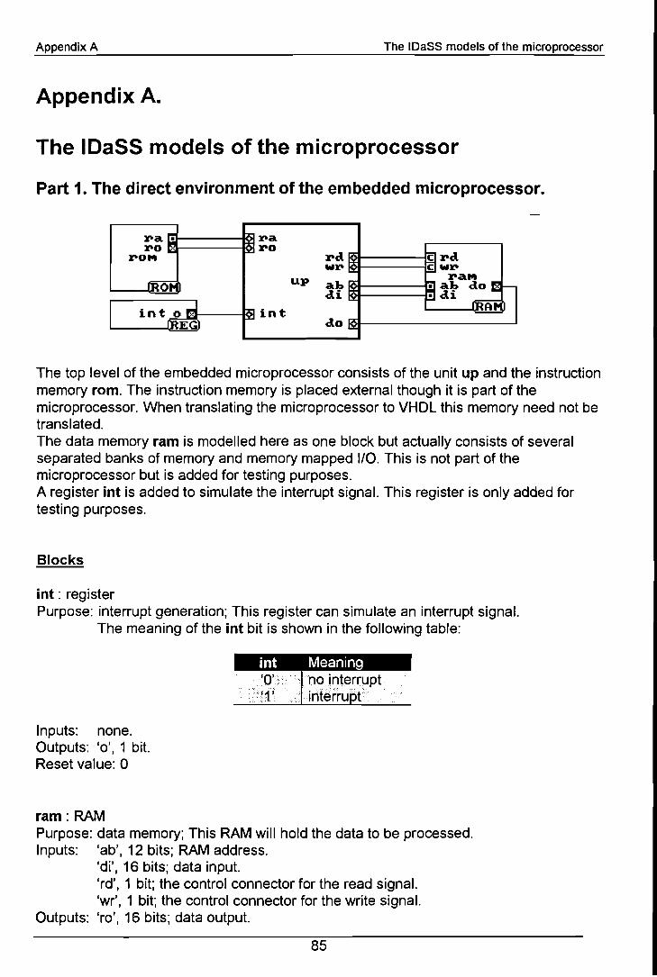
Appendix A
Appendix A.
The IDaSS models of the microprocessor
The IDaSS models of the microprocessor
Part 1. The direct environment of the embedded microprocessor.
:ra:ro
:rd c :rdw:r c w:r
up :raMah • ah dodi • di
int A
do
The top level of the embedded microprocessor consists of the unit up and the instructionmemory rom. The instruction memory is placed external though it is part of themicroprocessor. When translating the microprocessor to VHDL this memory need not betranslated.The data memory ram is modelled here as one block but actually consists of severalseparated banks of memory and memory mapped 110. This is not part of themicroprocessor but is added for testing purposes.A register int is added to simulate the interrupt signa!. This register is only added fortesting purposes.
Slacks
int: registerPurpose: interrupt generation; This register can simulate an interrupt signa!.
The meaning of the int bit is shown in the following tabie:
Inputs: none.Outputs: '0', 1 bit.Reset value: 0
ram: RAMPurpose: data memory; This RAM will hold the data to be processed.Inputs: 'ab', 12 bits; RAM address.
'di', 16 bits; data input.'rd', 1 bit; the control connector for the read signa!.'wr', 1 bit; the control connector for the write signa!.
Outputs: 'ro', 16 bits; data output.
85

Appendix A
Size: 4096 x 16 bitsTechnology: IDaSS default technology.
System-defined timing for control input 'rd':Bus to command delay: 6n sec.
The IDaSS models of the microprocessor
•.••.•••...•.•.•.••••. < .... ······<1
System-defined timing for control input 'wr':Bus to command delay: 6n sec.
Delays:Addr. to output delay (async): 25n sec.Clock to (addr.) output delay: 20n sec.Port address setup time: 20n sec.Port command setup time: 18n sec.Clock to (fixed) output delay: 15n sec.Write data setup time: 30n sec.
rom: ROMPurpose: program ROM; It contains the instructions that must be executed. It's default
function is 'read' .Inputs: 'ra', 12 bits; ROM address.Outputs: 'ro' I 16 bits; ROM output.Size: 4096 x 16 bitsTechnology: ASA synchronous read only memoryDelays:Addr. to output delay (async): 35n sec.Clock to (addr.) output delay: 15n sec.Port address setup time: 30n sec.Port command setup time: 20n sec.
up : schematicPurpose: the actual microprocessor. For a more detailed description see part 2.
86

Appendix A
Part 2. Description of the schematic up.
The IDaSS models of the microprocessor
int ba ba Ja Jaad ad
Ir'A dj. dj. 9S 9SiC ie aC aC
1r'0 d2 d2 air' air'Ma Ma
Cetch decode execute "Ir'i tebacksd sd
idi .. id id ie iet~MObasC
Connectorsname 1/0 bitsab 0 12di 0 16block.do 16RAM.int I 1ra 0 12rd 0 1block.ro 16ROM.
descriptionaddress bus; generated by the execute block.data in; data to be stored in the RAM; generated by the execute
data out; data loaded from the RAM; generated by the external
interrupt signa!.ROM address; generated by the fetch block.the read signal for the external RAM; generated by the execute
ROM output; the instruction read from the ROM; generated by the
wr 0block.
Blocks
1 the write signal for the external RAM; generated by the execute
decade : schematicPurpose : The pipeline stage named decode. This stage receives the instruction from
the fetch stage and decodes the instruction.
execute : schematicPurpose : The pipeline stage named execute. This stage operates on the data
generated by the decode stage. The result is written to the external RAM orpiped to the writeback-stage.
fetch : schematicPurpose : The pipeline stage named fetch. This stage generates the next instruction
address and receives the instruction from the ROM. This instruction is pipedto the decode stage. This pipeline stage also contrals the interruptmechanism.
87

Appendix A The IDaSS models of the microprocessor
writeback : schematicPurpose : The pipeline stage named writeback. This stage writes the result from the
execute stage back to the registers of the decode stage. The flags aremodified and the branch signaI is generated by this stage.
Part 2.1. The description of the schematic fetch.
[.c.]OP
Connectorsname 1/0 bitsad 0 12ba I 12branch.br I 1id I 16ie I 16if 0 16int I 1iw I 16mo I 16ra 0 12ro I 16sf I 1
descriptionthe address of the next instruction.branch address; the address to jump to in case of a conditional
the branch signa!.the instruction present at the decode stage.the instruction present in the execute stage.the instruetion generated by the fetch stage.the interrupt signa!.the instruction present in the writeback stage.memory out; the output of the RAM.ROM addressROM output; this is the instruction fetched from the ROM.the stall signal for the fetch stage.
88

Appendix A
Blacks
The IDaSS models of the microprocessor
amux : operatorPurpose: address multiplexor; This multiplexor switches between the 'next instruction
address register' (nia) and the 'program counter save register' (pcs). Theoutput of this multiplexor will be piped to the decode stage. It can be saved onstack or used to calculate the branch address. The functionality is shown inthe following tabie. Switching between the two functions is controlled by thefinite state machine controller intctrl.
Inputs: 'nia', 12 bits; next instruction address.'pcs', 12 bits; program counter save.
Outputs: '0', 12 bits; output of multiplexor.
IDaSS description:
System-defined timing for output '0':
Data transfer delay: 2n sec
System-defined output multiplexor delays:For output '0': 4n sec
Text for function nia:
Text for function cs:"select pcsave-register"
~:ipcs·•. ··•·····
imux : operatorPurpose: instruction multiplexor; This multiplexor has three functions which are
controlled by the finite state machine controller intctrJ. One of these functionsis the generating of the nop instruction. Another is the generating of the intinstruction. The third function is named normal and is an ordinary multiplexorfunction which switches between the two inputs 'rom' and 'si'. Switchingbetween these two inputs is controlled by the input signal 'sic'. This is shownin the following tabie.
89

Appendix A
function sic si nal out ut value
The IDaSS models of the microprocessor
ipt··.·.·····\\>hdp .•••.••••...•...
. ./ ·1······.··norma
valueFFD7h ..yall.leFFFFh .•..frómihput rOm··fromiriutsT>
Inputs: 'rom', 16 bits; instruction from ROM.'si', 16 bits; saved instruction.'sic', 1 bit; control signal to select between input 'rom' and input 'si'.
Outputs: 'if 1 16 bits; instruction generated by the fetch stage.
IDaSS description:
System-defined timing for output 'if:Data transfer delay: 2n sec
System-defined output multiplexor delays:For output 'if: 4n sec
Text for function 'int':"eall iriterrüpt routine"
Text for function 'nop':"irïsèrt ärïdpinstruction"
it:=%1111111111111111
Text for function 'normal':"no interruptcall"......::.. «::::::-:-:-..
.... ':-:-:- "':-:::................... .."
if := sic ifO: rom.... ift: si
Internal time delays for function 'normal':From 'rom' to 'ir: Sn secFrom 'si' to 'ir: Sn secFrom 'sic' to 'ir: Sn sec
inc : operatorPurpose: incrementor; This operator increments its input value.Inputs: 'i', 12 bits.Outputs: '0', 12 bits.
IDaSS description:
90

Appendix A
System-defined timing for output '0':Data transfer delay: 2n sec
Text for function 'increment':
The IDaSS modeIs of the microprocessor
Internal time delays for function 'increment':From 'j' to '0': 11 n sec
intetrl : state machine controllerPurpose: interrupt controller; In case of an interrupt it takes care of saving the right
return address on the stack and activates the interrupt routine at the propertime.This finite state machine controller controls the logic blocks amux, imux andpeso The controller consists of 11 states. The function of the controlled blocksis shown for each of the states in the following tabie.
123·45678910
.... 11
loadIbadload·
··holdloadloadholdholdholdloadload
In the following figure the state transition diagram is shown. The condition 'idjmp' meansthat there is a jmp instruction in the decode stage (ie: execute stage; iw: writebackstage). The condition 'idbr' means that there is a conditional branch instruction in thedecode stage.
91

Appendix A The IDaSS models of the microprocessor
stall-br-iebr-idjmp +
stall-br-idjsr +
stallobr
br
stall-br-(idbr + iebroidjmp)1-------.;....---..;..-...... 7
stall-br-iebr-idjmp
stall
stall-br-idrts5
int-stallobr +
int-staii-broiwrts +int-stall-br-idjsr +
int-stallobroidjmp-iebr
int-stall-br-idbr +int-stallob'r-iebroidjmp
stall-idbr-idrtsoidjmp-idjsr
A short description of each state:
State 1:This is the initial state where it will remain as long as there is na interrupt signa!. If aninterrupt signaI appears at the time of a stalI, na state change will occur until the stallsignaI is passive again.
State 2:State 2 inserts a nop instruction to enable the right flags to be saved on the stack.
State 3:In this state the int instruction is generated.
92

Appendix A The IDaSS models of the microprocessor
State 4:This stage will be entered if the decode stage contains a conditional branch instructionor the execute stage contains a conditional branch instruction without a jmp instruction inthe decode stage. The pcs register holds the return address in case the branch is nottaken.
State 5:If the decode stage contains an rts instruction the pipe must be drained and nops areinserted to retrieve the return address from the stack. This address will be saved on thestack again as the return address of the interrupt routine.
State 6:If the execute stage contains an rts instruction (the decode stage will always contain anop instruction in this case) the pipe must be drained and nops are inserted to retrievethe return address from the stack. This address will be saved on the stack again as thereturn address of the interrupt routine.
State 7:If a branch occurs the branch address must be saved as the return address and it takesanother 'wait state' (state 2, a nop instruction is inserted) to let the program counter loadthe return address. If no branch occurs and there is no conditional branch instruction inthe execute stage the interrupt instruction can be started (state 3). But if the executestage does hold a conditional branch instruction it must first be evaluated (state 8).
State 8:If a branch occurs the branch address must be saved as the return address and it takesanother 'wait state' (state 2, a nop instruction is inserted) to let the program counter loadthe return address. If no branch occurs and there is no conditional branch instruction inthe execute stage the interrupt instruction can be started (state 3).
State 9:This state is entered if there are no instructions in the decode, execute and writebackstage that can change the program counter contents. At this state the decode stage isloaded with an instruction which was already fetched from the instruction memory. Thisinstruction must be examined to see if it can change the 'normal' program flow (canchange the program counter contents: conditional branches, jumps, etc.).
State 10:This state is entered if the decode stage contains a jmp instruction and the executestage contains a conditional branch instruction. At this state the conditional branchinstruction has moved to the writeback stage and it will be clear if the branch is to betaken (state 2 is next state) or not (state 3 is next state).
State 11:As this microprocessor does not allow for nested interrupts, this state will not be left untilthe rti instruction is executed.
The IDaSS description:
This state machine controller has 11 states.
93
Appendix A The IDaSS models of the microprocessor
No stack is available for 'subroutine' calls.This controller is enabled following system reset.
This state machine controller has no connectors.
System-defined timing for this state machine controller:Clock to state delay: 15n secState/test to command delay: 10n secTest to clock setup time: 25n sec
. ,... . .
·§i~i~·1··:··..·.·.· ·· · ··.········· .iniuxnOrmál;pèSload; ..amuXniá: ...[ sf "is there á stalI"I %1~> state11%0 .
... [ iregi'is there an interrupt"·1 %0 '7>staté1
1%1« .<.> [btllisthefe an active branch".·1%1..;>stafe41%0< .[_idbr:= ((id from: 13 to: 15)=%101)._idbr"is there a branch instructionin id"%1'7> státe4%0[_iêjump:=((ie from: 13 to: 15)=%100)._iejurhp "does ie contain a jsr Or jmp instruction"
1%1 ->.state31%0/ .....••... . .
....idJsr:= ((id frölll: 12 to:15)::::%i Obi) .•....«~i ....idjsr"does id contäina jsrihstructiön" ..
ii~i(:il;~~i'lLI;~i~1,~;.:~31~:;'if~~j!~i!~:liiI7:!;!;••••••••••••••••••••••••••••••••••••••••••••••••••••21~~~ •••,~.~Z~1~~n~~i.;);~W~ ••~~~.trJciio;,I ••••••.•••••••••••••....•.•••..•..
1~6-0s~~te2 </ .... ••••.••..••.•.... •··i .. .... ..... ...• .•... ./ ... . .
.r.....îerts := (((ie from:13 to: 15)=%111) /\ .
••••••••••••••••••••••••••••••••••••••••••••••••••••••••••••••••••••i·~rts ••·,,~~tZ1:~în~~:i;~~o/rt:1·i~~t·ructio.h" ...
7jii:l!ij;i:l"pX~:s:t~I&;i~;:ró~.~~;~;:i!~;~~;~~J{i'"·((id from: 3t6: 5)=%110)):<·
94
Appendix A The IDaSS models of the microprocessor
Internal time delays tor this state:From bloek 'id' to '_idbr' in test #4: 6n secFrom bloek 'ie' to '_iejump' in test #5: 6n secFrom bloek 'id' to '_idjsr' in test #6: 6n secFrom bloek 'iw' to '_iwrts' in test #7: 9n secFrom bloek 'ie' to 'Jerts' in test #8: 9n secFrom bloek 'id' to '_idrts' in test #9: 9n secFrom bloek 'ie' to '_iebr' in test #10: 6n secFrom bloek 'id' to '_idjmp' in test #11: 6n secFrom bloek 'id' to '_idjmp' in test #12: 6n sec
Text tor state number 2:"ThisiSstate2" .
f!rf!~~!«I .•·•.II··~6gî(raO&;/ .•.••..•.. / ..8rilUx pcs;«·•.....•...•.... <·······1>5tate3//········
95
Appendix A The IDaSS models of the microprocessor
Text tor state number 3:"thiSi5 state 3n
·~~!t~~: ••••••••••••••••••• ••••·•••••·.••••••••·••••••••........................................imûXnbp;/ .pcshold; .....al11uxptS;[ sf "is thare astall"1% 1 -> stata4r%Ö ... [ br "is there a branch to be taken"I%1<·>state21%0/> ....
<1Jdb(:::: ((id trom: 13 to: 15)=%101).,-idbr "isthere a branch instructionin id"
I %1 L>state7....• J%0 <:.. .. . .
··f_idjsr:= ((id trom: 12 to: 15)=%1001).>.........·LJdjsr "does id containa jsr instruction"
>1~6->state2 .. ..••.••.. ......•..•••. .
... ..... [ ....idrts := (((id trom: 13 to:15)=%111) 1\/
..........>.. . ((id trom: 3to: 5)=%110)). .i idrts"doesid cohtain anrtsirîstruetióni
,
.<.1%12> state5 ..
lr~ebt:;:. ((ie trom:· 13 to:15)=%1 01 ).<<:>iébf"isthereabrahèhinstrUë:tióriTn ié">·../
.......U\ J·••~1<: · ·.·.................. ............</ >•.••••••.•••..•••••. ·· ••••••••••.•i· · ·.· / <: ••••.•••••.•••••••••••••••••••••••••••••••••••••••.
TJdjrnp:=((i(nróm:12tq:15)~%1000).< ....>y·.·.y ..••..·· .•·•· ..·•·•·•···.....idjlTlp ·"doès···id·.•cóhtäina.Jmp···ihstr'OèHóhîî
·..••••••••••••••..i I %t b staté1 0 •••••...... . ... ... . ..... ... ... ...
<[%9 ~;stàtaT . .
l;l!!!i;tH~):~!i{(i~'tioffi·:.12 tb:;15)~~!~~r:/2.idjl1lp "does idcontaihájl1lpirystfüdión"<:.<J%1;;':>state2. . ..
1············<f%03 statè3.... ········<:·· ·1········ .
96

Appendix A The IDaSS models of the microprocessor
Internal time delays tor this state:From bloek 'id' to '_idbr' in test #3: 6n secFrom bloek 'id' to '_idjsr' in test #4: 6n secFrom bloek 'id' to 'Jdrts' in test #5: 9n secFrom bloek 'ie' to '_iebr' in test #6: 6n secFrom bloek 'id' to '_idjmp' in test #7: 6n secFrom bloek 'id' to '_idjmp' in test #8: 6n sec
Text tor state number 5:"This is state 5"
...... :-:-:-: :-
state5:··imux nop;.p~~I?ad;
arnuxpes;:'>state6
Text tor state number 6:"This is state 6"
state6:>iml.J)(!1op; ..pes load;amux pes;->state2
Text tor state number 7:
· .... :- .-:::: ..:-::.:::::::::::: .
«·1>1
"This is state 7"
st~t~;': •••••••••• ••••••••••••••••••••••••· •••••• •••·•·ImÛ)(hOp;<.pcshOlêJ;~mÛxp(;§: > •••••.••••
[bf"islHêfea branch" ..l%r"~státé2 .
Tr~ebr:=((ietr6m:13t6: 1S)~%101} .. iébf"döesié eontaina eonditiönal branchlnstruetión"
l%f S state8 . .1%Ö ..>sfate3 ....
I]i)I]q·····
97

Appendix A
Internal time delays ter this state:From bleek 'ie' te '_iebr' in test #2: 6n sec
The IDaSS models of the microprocessor
Text ter state number 9:"This is state 9"
............:.-:
stat~9:Îrnux nop;pèShOld;äIllUxpcs;·.·.lSf"is thèreà sfall"T%f s stàtè91°A:0
r2ridjUrTÎW:f:((id trem: 13te: 15)=%100). .. <>j.JdjullIp "does id eentain a jmp er jsrinstruCtien"
I% 1;'> state2
1%0··· ........·~;\L>. .•.. ... /.... , -0
l;;;..ldbL,~ ((Id trem. 13 te, 15)- %101). / ... ....Lidbri'deès idcentain a eenditiOrlálbraneh instruétien"
~>·statê7
Internal time delays ter this state:Frem bleek 'id' te '_idjump' in test #2: 6n secFrem bleek 'id' te 'Jdbr' in test #3: 6n secFrom bleek 'id' te '_idrts' in test #4: 9n sec
98

Appendix A The IDaSS models of the microprocessor
Text for state number 11:"This is state 11,wait until theinterrupt""servicE! routine has ended."
sfate1 :imuxhormal;pcsload;)amuxhia' .,[_iwrtT:=((iw from: 13tó: 15)=%111) A
) ((iwfrom: 3 to: 5)=%100)......iwrti "islheihterrupt routine finished"
I %0 ..::>statel1I %f"'>state1] .
Internal time delays for this state:From block 'iw' to '_iwrti' in test #1: 9n sec
ireg : registerPurpose: interrupt register; This register first synchronises the external interrupt. The
value of the register contents is read by the state machine controller intctrl.
Inputs: ei', 1 bit.Outputs: none.
IDaSS description:
Default function: 'Ioad'Reset value: 0
System-defined timing for this register:Clock to data delay: 8n secClock to status delay: 7n secData setup time: 12n secCommand setup time: 7n sec
99

Appendix A The IDaSS models of the microprocessor
namux : operatorPurpose: next address multiplexor; A5-input multiplexor which is controlled by namuxc.
One of the inputs is generated internally. The following table shows thefunctions of this block.
function control value select in utsela4 ... ·.·000 ..seh:f1··············/ OOf
•.•.•.•...•.•..•.•...•..•...•.•.•.•.•.•..•.•.•..•.•..•.•..•.•..•..•.•.•s~.e.e.••••.• ·~.•.:.••.••.•~.......••.•.•••....•.•••.•.••.••...•.•.•.. >.•.••..( ..•.•.. <. 010>i°1······xx11 .•.·•.•..•..•.·.•.·....•.•...·.•.· .. seliht·
.... load incremented program counterlead JUmpàddress« . ...............>
< ::~;(H<llóad+efurnàddresSi··.
;6~~~~?~~t~r~~~Jd~r~~s~81~+Inputs: Ca1', 16 bits, only 12 bits are used; the jump address.
'a2', 12 bits; the branch address.'a3', 16 bits, only 12 bits are used; the return address.'a4', 12 bits; the incremented program counter.cc', 3 bits; the control input connector.
Outputs '0', 12 bits.
IDaSS description:
System-defined timing for output '0':Data transfer delay: 2n sec
System-defined output multiplexer delays:For output '0': 7n sec
Control s ecification:"select an input of the multiplexor"
-,,: :.: : .
%000séla4.%001séla1.%OfOsela3.%01fsela2./%100·selirif·
System-defined timing for the control input cc':Bus to command delay: 6n sec
Text for function 'sela1':"~êlecfinpl.Jfä1 :thé jump address'\ ....... .. , .. " -, ..
Text for function 'sela2':I"selectinpÛra2:branchaddress"/II>·> . .... . I
I_O_:=_à_2_·~-",---",---",---",---",---",---",---",--=.=.;.-",---",---",---",---",---",--_-",---",---",---",--I
100
Appendix A
Text for function 'sela3':"sélect inputa3: return
·S••• :.@·.•·~·~···f~O~:····O ··t6:·····;··1················
The IDaSS models of the microprocessor
Text for function 'sela4':"selecfinplJt .:llA·n......n'.:lllinr·..6,Yioln+.:ll+inln"· •
•~•••:.I••• ä~............................................. . ,···~·~·ï••·••• ·••••••••••••••••••••••••••••••••••••••••• /. i >< >••••••••••••••••••••••••••
Text for function 'selint':"generàte the interruptroutine start áddress(001h)"
namuxc : operatorPurpose: next address multiplexor controller; This operator controls the multiplexor
namux.
Inputs: 'br' I 1 bit; the branch signa!.'id', 16 bits; the instruction in the decode stage.'iw', 16 bits; the instruction in the writeback stage.
Outputs: '0', 3 bits;
IDaSS description:
System-defined timing for output '0':Data transfer delay: 2n sec
Text for function 'doit':"this operator controls the next program counter"'iàddress multiplexer.""c(OOO)= a4 :normal incrememtatiol1". .."c(001)==a1: loadjump address"} ../<"c(010):: 83 : load retur~ áddréssl.>/ ."<::(911) ==à2:10àd bràrichaddress">···· .';6(100rSloádintérruptstartáddrêss(()Ö15),'·
"~~~•••• I§·••··1·····.i·~····c~s·~ ••••id····i·s·· a· js.r.··6r.j·~p •••igstr~8ti.()g" ••••••••••••••••••••••••••••••••••••••..•....•...:imp:==((idHóm:1310:1S)== %100). .. .... .....'ifêfls1ifiWis a rtsofrti instl"lJction"lr~t::::({iWfrom:13 to:15) = %111) /\(iwat: 5)/\ ((iwat: 3)not)."il1fis firicase id is an interrupt caH" ...... ..•...... ....:inf:::«idfrom: 13 tO:f5)= %111 )]\(idJr(jf1Î:áto:5)=%01 0)."h6fê:executiortOfrts or rti·insèrts4hopsihlhe<decodestagé.ii
"S6..Jmpáhd ret· can notbeactivêáfthesámélirhé" .."/ihrcanriot beàctivetogetherwith at5ránêh,.:impbr __rts"
101

Appendix A
!6i=inf,(bfV ret),(br'V..Jmp)Internal time delays for function 'doit':
From 'id' to '..Jmp': 6n secFrom 'iw' to '_ret': 12n secFrom 'id' to '_int': 9n secFrom '..Jmp' to '0': 3n secFrom '_ret' to '0': 3n secFrom 'br' to '0': 3n sec
The IDaSS models of the microprocessor
nia : registerPurpose: next instruction address; As the instruction memory is a synchronous ROM
the 'next instruction address' that accompanies the instruction must be piped.This is done by this register.
Inputs: 'i', 12 bits;'c', 1 bit; the control connector
Outputs: '0', 12 bits;
IDaSS description:
Default function: 'Ioad'Reset value: 0
Control s ecification:"holdwhehstalled"
.. .,)t... <\::»<\:»:r .:::. :.. -:."%Oload.%1hold
System-defined timing for control input 'c':Bus to command delay: 6n sec
System-defined timing for output '0':Data transfer delay: 2n sec
System-defined timing for this register:Clock to data delay: 8n secClock to status delay: 7n secData setup time: 12n secCommand setup time: 7n sec
pc : registerPurpose: program counter register.
Inputs: 'j', 12 bits.'c', 1 bit; the control connector.
Outputs: '0', 12 bits.
102

Appendix A
IDaSS description:
Default function: 'Ioad'Reset value: 0
Control s ecification:"hold whënstalled" ...
i6···ig·~~ .•••••••••••••• •••••••••·· .........••••••••••••••••••••.•......•....................................%1holä>\.··· .
System-defined timing for control input Cc':Bus to command delay: 6n sec
System-defined timing for output '0':
Data transfer delay: 2n sec
System-defined timing for this register:Clock to data delay: 8n secClock to status delay: 7n secData setup time: 12n secCommand setup time: 7n sec
The IDaSS models of the microprocessor
pcs : registerPurpose: program counter save register; In some cases, when an interrupt occurs, it is
necessary to save the contents of the program counter. It will then be saved inthis register. This register is controlled by the state machine controller intctrl.
Input: 'i', 12 bits.Outputs: '0', 12 bits.
IDaSS description:
Default function: 'Ioad'Reset value: 0
System-defined timing for output '0':Data transfer delay: 2n sec
System-defined timing for this register:Clock to data delay: 8n secClock to status delay: 7n secData setup time: 12n secCommand setup time: 7n sec
103

Appendix A The IDaSS models of the microprocessor
si : registerPurpose: save instruction; In case of a sta 11 the instruction memory can not 'hold' its
current output. To prevent the data to be lost on the next clock the data issaved in this register. After a sta 11 the multiplexor imux selects the output ofthis register to generate the next instruction. This register is controlled by sic.
Inputs: 'I', 16 bits.'c', 1 bit; the control connector.
Outputs: '0', 16 bits.
IDaSS description:
Default function: 'hold'Reset value: 65535 (OFFFFh)
Control s ecification:"this signal contrals the 'save instruction' register"
%Oioàd.%lhold/
System-defined timing for contraI input 'c':Bus to command delay: 6n sec
System-defined timing for output '0':Data transfer delay: 2n sec
System-defined timing for this register:Clock to data delay: 8n secClock to status delay: 7n secData setup time: 12n secCommand setup time: 7n sec
sic: registerPurpose: save instruction controller; In case of astall the output of the instruction
memory must be saved. During the first clockcycle of astall, the 'hold' controlsignal must be postponed one clock cycle to enable the si register to load theoutput of the instruction memory.
Inputs: 'I', 1 bit.Outputs: '0' I 1 bit.
IDaSS description:
Default function: 'Ioad'Reset value: 0
104

Appendix A
System-defined timing for output '0':Data transfer delay: 2n sec
System-defined timing for this register:Clock to data delay: 8n secClock to status delay: 7n secData setup time: 12n secCommand setup time: 7n sec
105
The IDaSS models of the microprocessor

Appendix A The IDaSS models of the microprocessor
Part 2.2. The description of the schematic decode.
EJ1sd
Io"~ 1.:-1.. sd: L. sd ~,!j:- ~+it..j- ~iit~!tr:- i. ~itcct..C Iel
.talli.
fcUî st - - stQ\i
I 1.1
I I ~• I If 0ad ad
ad...g add...I'ii"i'/; • id out Ioa
B • d2
"'"1- I
B ~ ~ ael b 0 r=:rE]~ el1..u>c
~Iaid dlil~~d .11 r=:~l!Jd1 oJ. r.t .IJ. /i\ii
gp.... l d21i~ I:Jd2ir i oll! I-- s2J!~~sZ "h..u>c
Id"~1J OP03 - EJ
l'iiVCPR 9-
:"iel ~ ~aoQ<i!des"uK
I!JI .. d.~l:Jd".OP ~din
~
~fl ~ IiU• 1W 0
a dinMuK
1F~::: /Ni
a I~
t:1.,tZ add.. r=:Br:- Id
ic'id ~aelel.... 1
5prhm"~IJS~~ Ii
~~sd o. • I'ego
Iffi "'""'9'.
~ oll! ,....-!adat- ~ sprlo
regMux...ooii
l~d1 'OP
Connectorsname 110 bitsad I 12ao I 16ba 0 12br I 1d1 0 16d2 0 16id 0 16ie I 16if I 16iw I 16ma 0 12mo I 16sd 0 1sf 0 1
descriptionnext instruction address.ALU output.branch address; used in case of a conditional branch.the branch signa!.data1.data2.instruction in the decode stage.instruction in the execute stage.instruction in the fetch stage.instruction in the writeback stage.memory address of the data memory.memory output of the data memory.the stal! signal for the decode stage and execute stage.the stal! signal for the fetch stage.
106

Appendix A
Slocks
The IDaSS modeIs of the microprocessor
adder: operatorPurpose: This block contains the adder which calculates the branch address. The
branch address is calculated by adding the displacement to the nextinstruction address. The displacement is formed by bits 4 to 11 of theinstruction word id extended to 12 bits. This adder is also used to decrementthe contents of one of the General Purpose Registers in case of a filJinstruction. The operator decctrl controls the switching between these twofunctions. The functions are shown in the following tabie.
Inputs: 'ad', 12 bits; the address of the next instruction.'c', 8 bits, only bit 0 is used; the control connector.'d2', 16 bits; data2.'id', 16 bits; the instruction in the decode stage, containing the displacement.
Outputs: 'out' I 12 bits;
IDaSS description:
System-defined timing for control input IC':Bus to command delay: 6n sec
System-defined timing for output 'out':Data transfer delay: 2n sec
System-defined output multiplexer delays:For output 'out': 4n sec
Text for function 'add':
107

Appendix A
Internal time delays for function 'add':From 'ad' to 'out': 11 n secFrom 'id' to 'out': 11 n sec
The IDaSS models of the microprocessor
Internal time delays for function 'decr':From 'd2' to 'out': 11 n sec
addrsel : operatorPurpose: address selection; This operator contains the adder to calculate the effective
address of the data memory. The adder is also used to decrement orincrement the contents of the Stack Pointer Register. This operator has 4functions which are shown in the following tabie. Switching between the 4functions is controlled by decctrl.
Inputs: 'c', 8 bits, only bits 6 and 7 are used; the control connector.'d2', 16 bits; data2.'id', 16 bits; the instruction in the decode stage.'rego', 12 bits; the output of the registers DBRlIBRISPR.
Outputs: 'addr', 12 bits; the effective address of the data memory.'spfb', 12 bits; the stack pointer feedback value.
IDaSS description:
108

Appendix A
System-defined timing for control input 'c':Bus to command delay: 6n sec
System-defined timing for output 'addr':Data transfer delay: 2n sec
System-defined timing for output 'spfb':Data transfer delay: 2n sec
System-defined output multiplexer delays:For output 'addr': 4n secFor output 'spfb': 4n sec
Text for function 'direct':"dêtéfrhihêdirectaddreSS".. .. . .
ad~·~·•••~·I.· ••~~.~.~ •..•+·..(6··.·z~roesl •••••(id frórn:···.6••••tO:•••••1•.·1••))..spfb:=Q< ..
Internal time delays for function 'direct':From 'id' to 'addr': 11 n secFrom 'rego' to 'addr': 11 n sec
Text for function 'indexed':"dëtêhhfriëindexed address"
äd~r:::rego+ (d2 trom: 0 to:11).spfl:):;§O .
Internal time delays for function 'indexed':From 'd2' to 'addr': 11 n secFrom 'rego' to 'addr': 11 n sec
The IDaSS models of the microprocessor
Internal time delays for function 'pop':From 'rego' to 'addr': 11 n secFrom 'rego' to 'spfb': 11 n sec
109

Appendix A The IDaSS models of the microprocessor
Internal time delays for function 'push':From 'rego' to 'spfb': 11 n sec
adreg : registerPurpose: address register; Part of the pipeline register between the fetch stage and the
decode stage. This register holds the address of the next instruction. Thisregister is controlled by the stall signal for the fetch stage, generated by logicblock stall.
Inputs: 'c', 1 bit; the control connector.'j' I 12 bits.
Outputs: '0', 12 bits.
IDaSS description:
Default function: 'Ioad'Reset value: 4095 (OFFFh)
System-defined timing for control input 'c':Bus to command delay: 6n sec
Control s ecification:
,,9ri~~~~lrbold this register"
••~8.··,§~d •.•••••••••••••••••••·····%1hOlêf
System-defined timing for output '0':Data transfer delay: 2n sec
System-defined timing for this register:Clock to data delay: 8n secClock to status delay: 7n secData setup time: 12n secCommand setup time: 7n sec
d1mux: operatorPurpose: multiplexor for d1 ; A plain multiplexor in datapath d1 that switches between
data from the General Purpose Registers (output d1) and data from theaddress register adreg. Logic block decctrl contrals the switching between thetwo inputs. This is shown in the following tabie.
110
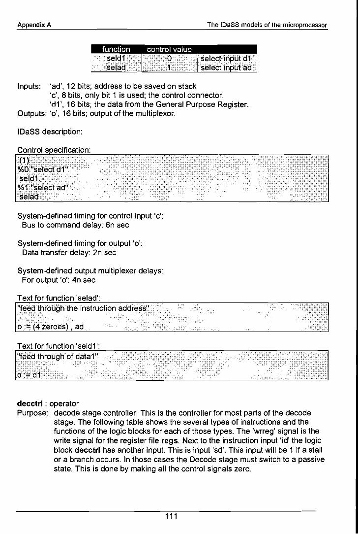
Appendix A The IDaSS models of the microprocessor
seleçfil'lp9tQtselé6fih ·üfád
Inputs: 'ad', 12 bits; address to be saved on stack"c', 8 bits, only bit 1 is used; the control connector.'d1', 16 bits; the data from the General Purpose Register.
Outputs: '0', 16 bits; output of the multiplexor.
IDaSS description:
Contral s ecification:- . .. . .···(·1··) .
:·0··.)[0······· .....·.'.. '.U.·.·····.·I••••••••••••••••t••••••••di1>;,.<· .70 . se ec .sêldi.<.···••X01i'~~I~êfad"·::sélädiii
System-defined timing for control input 'c':Bus to command delay: 6n sec
System-defined timing for output '0':Data transfer delay: 2n sec
System-defined output multiplexer delays:For output '0': 4n sec
Text for function 'selad':'1~~(jthröUghthe·instrucfion a·1ddr·es~s" ••• ·· ••·••·.·.·:·./\
~::::(4zeröes) , ad.. ..<\.:.:.:.......... :•••••...
decctrl : operatorPurpose: decode stage controller; This is the controller for most parts of the decode
stage. The following table shows the several types of instructions and thefunctions of the logic blocks for each of those types. The 'wrreg' signal is thewrite signal for the register file regs. Next to the instruction input "id' the logicblock decctrl has another input. This is input 'sd'. This input will be 1 if astallor a branch occurs. In those cases the Decode stage must switch to a passivestate. This is done by making all the control signals zero.
111
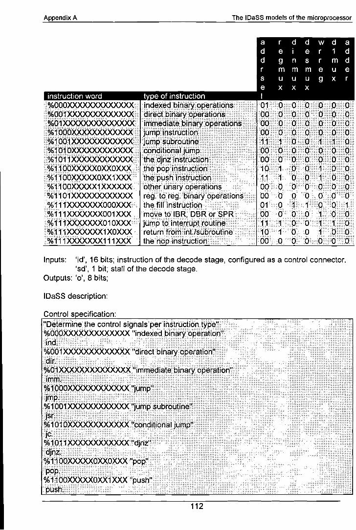
Appendix A The IDaSS models of the microprocessor
Inputs: 'id', 16 bits; instruction of the decode stage, configured as a control connector.'sd', 1 bit; stall of the decode stage.
Outputs: '0', 8 bits;
IDaSS description:
112

Appendix A The IDaSS models of the microprocessor
System-defined timing for control input 'id':Bus to command delay: 6n sec
System-defined timing for output '0':
Data transfer delay: 2n sec
System-defined output multiplexer delays:For output '0': 7n sec
Text for function 'filI':
113

Appendix A The IDaSS models of the microprocessor
Internal time delays for function 'fill':From 'sd' to '0': Sn sec
Text for function 'imm':"No.thingsp~cialfor immediate operätior'ls"/ ..
Text for function 'ind':"Indexed Binaryoperations" ..
114

Appendix A The IDaSS models of the microprocessor
Internal time delays tor tunction 'int':From 'sd' to '0': Sn sec
Text tor tunction "c':"Thêjûmpconditional operation"
Text tor tunction "m ':"Nothingspecialtor the jump operation" ..
115

Appendix A The IDaSS models of the microprocessor
Internal time delays for function 'jsr':From 'sd' to '0': Sn sec
Text for function' 0 ':
"Ihepopoperation"
Internal time delays for function 'pop':From 'sd' to '0': Sn sec
116

Appendix A The IDaSS models of the microprocessor
Internal time delays for function 'push':From 'sd' to '0': Sn sec
Text for function 're ':"Régistêtêinary operations"
Internal time delays for function 'regwr':From 'sd' to '0': Sn sec
117
Appendix A The IDaSS models of the microprocessor
Internal time delays for function 'return':From 'sd' to '0': Sn sec
:~:>-:-::<'.:\/.:.. . . ' ..".";."' ::...:::<:\.:.::.::":>:. <~«:/ .. -: "..
.... ......................tiêroeS,"address addérfuhttrbri"
.•••••••••••••••••••••••••••••••••••••••••••••••••••••1•••••~:~~:·:: ::~:t~i~~~t;·'BRlO·B·RlS.P·R" •. · ...
/«1 zeroès "data t6GPR oneif fill"•••••••••••••••.••••••••.••••... \>1.····zêroes:··"sèlect·..a.. <3PR,••• one••••if••ffll"./ .•
/<1zercès, ·"wHfeIBRl08R1SPR,,·····U·.>l:Z:èrbes, "data1.mux;; ..../> .
1zêroes ·;'ádêfèrSèlect, orie iffill"
desmux : operatorPurpose: destination multiplexor; Writing data to one of the registers of the General
Purpose Register (GPR) is mostly done by the writeback stage. In case of a tillinstruction the addressing is done by the instruction in the decode stage.Selection between these two is controlled by decctrl. The following tableshows the functions of this bloek.
··.?\\\.~~I.iW.·.·····················/sèlid
Inputs: 'c', 8 bits, only bit 3 is used; this is the control connector.'id', 16 bits; the instruction in the decode stage.'iw', 16 bits; the instruction in the writeback stage.
Outputs: 'des' I 3 bits; the destination register.
IOaSS description:
118

Appendix A The IDaSS models of the microprocessor
System-defined timing for control input 'c':Bus to command delay: 6n sec
System-defined timing for this output:Data transfer delay: 2n sec
System-defined output multiplexer delays:For output 'des': 4n sec
Text for function 'new':,irègTster~electionWith·fill operätiorl"<»··
. .. . ",.
............ . ."0":::::::::::::-::,., :. "' "
d~~:~icffrÓfr1:6tö:· 8
Text for function 'old':"(jé3Jäfrorpthe write back stage"
:::::::::::::::::::::::/:::::::::}:-.' : ,-::,', -":-..::: .. :::-:".' .
·d·~.~..•;.#••••ÎW··fr6fr1: .•••~ ··to:····2 ...
dinmux : operatorPurpose: data input multiplexor; It has 3 input busses to be switched to which means
that it needs 2 control lines. One of those control !ines comes from thecontroller decctrl. It switches between the output of the adder (at the top) incase of a till instruction and the output of the Write-back stage. The latterhowever can be the output of the ALU or the output of the Data Memory. Anextra control line is needed to select between those two inputs. This controlline is not fitted as one signal but as the instruction bus 'iw'. A function internalof dinmux determines which input must be selected. This internal signal wil1be called '_am' (ALU or memory). If it is zero, data from the ALU will beselected. If it is one, data from the Data Memory is selected. The functions areshown in the following tabie.
........ , ...
>äaàer
119
sèlèct..•iOPQt··8q···.......... ····1 : t •....'/.....•.•: ·t·.•...........,.<s~eclnpu. ·m.osèlêcfih urfl

Appendix A The IDaSS models of the microprocessor
Inputs: cao', 16 bits; ALU output.'c', 8 bits, only bit 4 is used; this is the control connector.'fl', 12 bits; the output of the adder in case of a fill instruction.'mo' I 16 bits; data memory output.'iw' I 16 bits; the instruction in the writeback stage.
Outputs: '0', 16 bits; the actual dat to be wriUen to one of the GPR registers.
IDaSS description:
System-defined timing for control input IC':
Bus to command delay: 6n sec
System-defined timing for output '0':
Data transfer delay: 2n sec
System-defined output multiplexer delays:For output '0': 4n sec
Text for function 'adder':"feedfhr6ughdata from adder"
0'" •••••• , • ..:::... :::::>..;::../:-..... ::::-.".-:'
B:~12~r()g~, fl
Text for function 'alumem':
aluor mem" . .. . ....memory toregistermove and in case ofapóp"
Internal time delays for function 'alumem':From 'iw' to '_am': 12n secFrom '_am' to '0': Sn secFrom 'ao' to '0': Sn secFrom 'mo' to '0': Sn sec
120

Appendix A The IDaSS models of the microprocessor
fbctrl : operatorPurpose: feedback control; This logic block controls the feedback multiplexor fbrnux.
Inputs: 'id', 16 bits; the instruction in the decode stage.'iw', 16 bits; the instruction in the writeback stage.
Outputs: '0', 3 bits;
IDaSS description:
System-defined timing for output '0':Data transfer delay: 2n sec
Text for function 'doit':t1fe~dbaêkcontr6rföl"thê~ëcod~stagê"<··
·.;;~~~•••~.· ••f:~~.~ •••••:··:~:J.~ •.••~h·~· •.~g~:~::...................... ...
"I~~rri ••••i.~· ...~·.....iR•••cá·;e··.8f··a.·••~.e~·0~ •••t8••·.registêf·••rll·00e····and· ·in···êasè••·8f a...pop,,···········
~~·~.~ ••••:.~ •••((iW· frOm:·····1.·4···to: .•15)••••=····%0()·.X·••«.i;··frQrn·: s···io·;····S). =·..%QOO))···V«(ivifrorii:12 to: 15)=%1 1ÖÖ) A«iWfrom:3tb: 0) =%OÖÖÖ));
u~fit~6~êktoa GPR" .. . .2binWriW:#«(iWfrorii:14 to:15)= %00)1\ «iW at3) = %O))V
< «(iwfröm: 14 to: 15)= %01) f\ «(iwfrom:3 to:5)~=%111»V"e)(cept I"m'...."<·.·.·.········.····<.«(iWfrom: 12to: 15) = %1101 )N((iw from: 3 to: 5)-::%111». "S",cept "mi"'''·.·.·.·.·
ÊlJHwfiw:=«iw from:12 tb: 15) = %1100)/\i < «(iwfrom: 3 to: 6) =0(00001) nqtJ~"allexcept a push"g8jf'lziw(:: «iwfrom: J? to:15)=%1{J1f), ..... .... ....
2~~\rJiÜI:=_binwriw V_unwriwV:ajrizi~.
Internal time delays for function 'doit':From 'iw' to '_mem': 9n sec (user-changed)From 'iw' to '_binwriw': 9n sec (user-changed)From 'iw' to '_unwriw': 7n sec (user-changed)From 'iw' to '_djnziw': 4n sec (user-changed)From '_binwriw' to '_rgwiw': 3n sec (user-changed)From '_djnziw' to '_rgwiw': 3n secFrom '_unwriw' to '_rgwiw': 3n sec (user-changed)From '_rgwiw' to '0': 6n sec (user-changed)From 'id' to '0': Sn sec (user-changed)From 'iw' to '0': Sn sec (user-changed)
121

Appendix A The IDaSS models of the microprocessor
fbmux : operatorPurpose: feedback multiplexors; This block contains two multiplexors. Each of the two
multiplexors switches between the output of the General Purpose Register,the output of the ALU and the output of the Data Memory. This block iscontrolled by fbctrl. The functions of fbmux are shown in the following tabie.
thormal>·······••··r> «'ir]> «>1 datäfrpriiGPR.y········ ·.·.~.at~.tpm~PRc•••••• >fBd1··atü··............. ·d~t~fr(jl1lAÇLJ> •••• >•••••••• <···•••••••••••.••.••••~at~ .••t9Jfl<3e.Ri) ••.•.••••••..f8êl1hiéhi) dátäffÓffiOátäMerftÓ ··········d···ff···············GPR···
......................................................... ··········aàtáff6n'lGPR<ury.•...•..•.•...•.•..••.••..•....•.•..•.•...•.•..•.•.•...••.•.•.•.••...••.•.•.•.•..••..••...••..•••.•.••...•.•.•••.••.•..••.•.dd.•••.•..•.•.••. aa•.
a
.•.•...••..•.tt·.•..•·.•.aaa.••·.•·.•..•.·.••·.•.·.•.•.·.•••f•.f
.•.·.•.·•.r~.•. ·.·.· ••·.·.60•.·.••...·.•.·.••.•.~m•.••.•..•.•.•..•....•.·.·.•.·.•.•..••••••A.D·.••.••.•.·•.·.•..•.·.•.La·.•••.·•·.•.•.·.·.t·.p.···.·a·.···....•··.•·•..•·•.•·•.•·••.•···..••.••·M·.·.··.·•.•·.• •.•··.•.••.• •.• •.··.·e···•.•••.••··.••.••·•..···.·.·.·m.•·• •.·· .••·•.•.••.•.•.•.•· •..•.•·•••.0···.•. •.•···..••.• ··•.••.•••.·.•.rv.·.·.·.•..·.•·.• •.·.··.•.·.·.·...•.•. •.·... ·.·...•...•...•...•.....•....•.•..•.....•.•..f~~~~~~~t~fç8mgpR) ... •.• ~1ftjt>CSm~I.~·...........dáfä.ffÓrft.ALU.· •••• C•••••••••••••••••••••••••.••••••..•.•••.•••.••..• dátà·frórft••·ALU••·••.••·.U
>fbb6thrfterft······· ···datà···itdh,···Oé3là···îVIéhib ···d~t~··frOm6ata···l\ÎlèmÖ············<····
Inputs: 'ao', 16 bits; the output of the ALU.'c', 3 bits; the control connector.'d1', 16 bits; data input 1.'d2', 16 bits; data input 2.'mo', 16 bits; the output of the data memory.
Outputs: '01', 16 bits; data output 1.'02', 16 bits; data output 2.
IDaSS description:
ecification:feedthrough"
System-defined timing for control input 'c':Bus to command delay: 6n sec
System-defined timing for output '01':Data transfer delay: 2n sec
System-defined timing for output '02':Data transfer delay: 2n sec
122

Appendix A
System-defined output multiplexer delays:For output '01': 4n secFor output '02': 4n sec
The IDaSS models of the microprocessor
123

Appendix A The IDaSS models of the microprocessor
GPR:RAMPurpose: General Purpose Registers; Thsi is a register file of 8 registers, each 16 bitswide.
Inputs: 'c', 1 bit; this is actually the write signal for the selected register.'des', 3 bits; the destination selection.'din', 16 bits; the input data for the selected register (des).'s1', 3 bits; address select for output 1.'s2', 3 bits; address select for output 2.
Outputs: 'd1', 16 bits; output 1.'d2', 16 bits; output 2.
IDaSS description:
This RAM uses the 'ASA 6-ported register file' technology.It contains 8 words of 16 bits each.There is no contents file attached.The contents are 0 after system reset.
Control s ecification:"Write.. regist~e'·· .
··O%1·•••·~;if~······.······················· .
System-defined timing for control input 'c':Bus to command delay: 6n sec
System-defined timing for output 'd1':Data transfer delay: 2n sec
System-defined timing for output 'd2':Data transfer delay: 2n sec
The functions of the (non-control) connectors are as follows:
Two Read-only ports:These port's technology is called 'ASA asynchronous read only port'.Cycle and mode settings are as follows:This port reads asynchronously.
System-defined timing for these read port:sAddr. to output delay (async): 12n sec
One Write-only port:This port's technology is called 'ASA synchronous write only port'.Cycle and mode settings are as follows:A write cycle takes 1 clock.The input must be valid when the write cycle is started.The memory cells are updated in clock cycle 1.The default writing command is 'nowrite'.
124

Appendix A
System-defined timing for this write port:Clock to (addr.) output delay: 20n secPort address setup time: 12n secPort command setup time: 12n secClock to (fixed) output delay: 15n secWrite data setup time: 16n sec (user-changed)
The IDaSS models of the microprocessor
gprsel : operatorPurpose: General Purpose Register select; Filter the addresses from the instruction in
the decode stage to select the two registers from GPR. This block is onlynecessary in 10aSS. In the actual circuit the input ports of the GPR can bedirectly connected to the appropriate bits of the instruction in the decodestage.
Inputs: 'id', 16 bits; the instruction in the decode stage.Outputs: 's1', 3 bits; address of the first port of the GPR.
's2', 3 bits; address of the second port of the GPR.
10aSS description:
System-defined timing for output 's1':Data transfer delay: 2n sec
System-defined timing for output 's2':Data transfer delay: 2n sec
Text for function 'select':]l~~I~(#!B~t~gistêrsfrQWJI1E:lln~ttücHgh"
••~.~••··.t~·.I~.·~~g~;· •••·()···t8:·.·2..·•·..•·•··.·· ..$~··i~iafrqm:6 to:S)·······
idctrl : state machine controllerPurpose: In some cases the instruction in the instruction register of the decode stage
must not be loaded with a new instruction on the next clock. In case of a stal!the instruction must be held. In case of some instructions nop instructionsneed to be inserted to guarantee proper operation of the piperine. This isdone by resetting the instruction register. In case the function of theinstruction register idreg (Ioad, hold, reset) must change, it must be donebefore the next clock. Therefor this finite state machine must be implementedas a Mealy Machine. The following figure shows the state transition diagram.The next function of the instruction register idreg is shown for each transition.
125
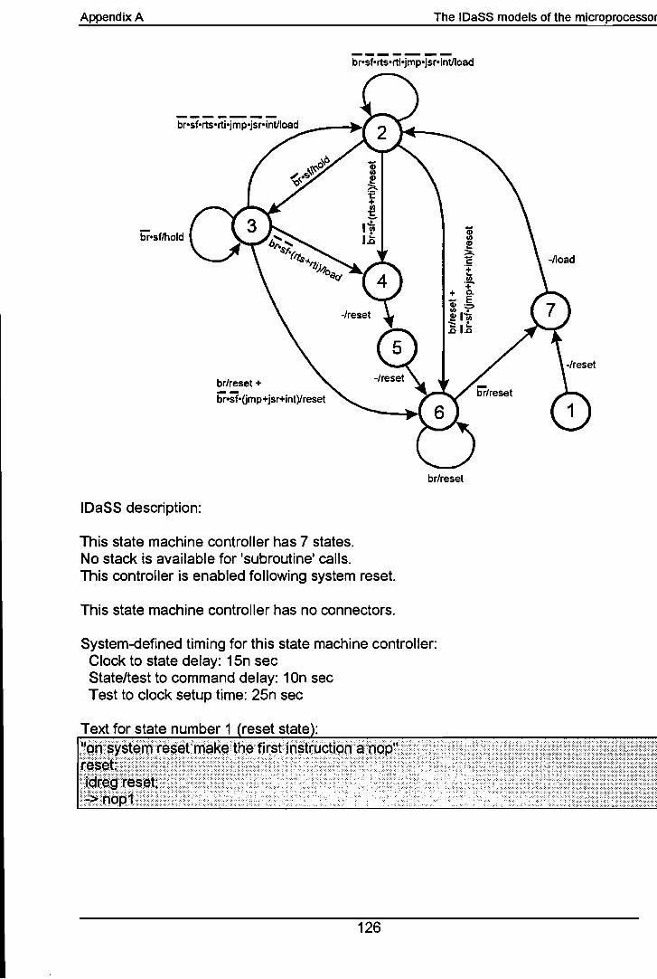
Appendix A
br-st/hold
IDaSS description:
br/reset +
j;-St-(jmp+jsr+int)/reset
The IDaSS models of the microprocessor
brost-rts-rti-jmp-jsr-intlload
br/reset
This state machine controller has 7 states.No stack is available for 'subroutine' calls.This controller is enabled following system reset.
This state machine controller has no connectors.
System-defined timing for this state machine controller:Clock to state delay: 15n secState/test to command delay: 10n secTest to clock setup time: 25n sec
126

Appendix A The IDaSS models of the microprocessor
127

Appendix A The IDaSS models of the microprocessor
128

Appendix A The IDaSS models of the microprocessor
Text for state number 6:
Text for state number 7:"insèrt1nop"popi.: ••••••••••••.•.•.••• ».·····iar~gI8ad;'::>honop/ ....
idreg : registerPurpose: instruction register for the decode stage; This register will hold the instruction
to be processed by the decode stage. It receives its contents from the fetchstage. In some cases it is necessary to hold the contents or to reset theregister. Control is done by the finite state machine controller idctrl.
Inputs: 'j', 16 bits;Outputs: '0' J 16 bits;
IDaSS description:
Default function: 'Ioad'Reset value: 65535 (OFFFFh)Reset command value: 65535 (OFFFFh)
System-defined timing for output '0':Data transfer delay: 2n sec
System-defined timing for this register:Clock to data delay: 8n secClock to status delay: 7n secData setup time: 12n secCommand setup time: 7n sec
129

Appendix A The IDaSS models of the microprocessor
regmux : operatorPurpose: register file data input multiplexor; This multiplexor switches between the data
from the data1 output of the General Purpose Registers and the stack pointerfeed back from addrsel. The following table shows the functions of this bloek.
Inputs: 'c', 8 bits, only bit 5 is used; the control connector.'d1', 16 bits; the data1 output of the General Purpose Registers.'spfb', 12 bits; stack pointer feedback.
Outputs: '0', 12 bits;
IDaSS description:
Control s ecification:~lê~t~SêlèCtion for·theIBR/DBRlSPR'i(5)<········...... .... ..•...•...........•..%phdatafrOrîi GPR"·dátät•.. ····••.................... ".. .
°%1 "dCifáfr-om adder"····fêêc:Jbaêk•••••••. <
System-defined timing for control input 'c':Bus to command delay: 6n sec
System-defined timing for output '0':Data transfer delay: 2n sec
System-defined output multiplexer delays:For output '0': 4n sec
Text for function 'data1':''Wtitédát?from a GPRtOa register"
·6•••:.~ •••d.i·.·.if()nî:.·.·.() to:.···1•• 1·•••••••••• ·•··············
130
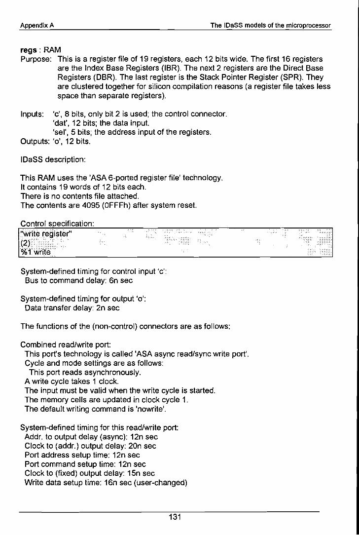
Appendix A The IDaSS models of the microprocessor
regs: RAMPurpose: This is a register file of 19 registers, each 12 bits wide. The first 16 registers
are the Index Base Registers (IBR). The next 2 registers are the Direct BaseRegisters (DBR). The last register is the Stack Pointer Register (SPR). Theyare c1ustered together for silicon compilation reasons (a register file takes lessspace than separate registers).
Inputs: 'c', 8 bits, only bit 2 is used; the control connector.'dat', 12 bits; the data input.'seI', 5 bits; the address input of the registers.
Outputs: '0', 12 bits.
IDaSS description:
This RAM uses the 'ASA 6-ported register file' technology.It contains 19 words of 12 bits each.There is no contents file attached.The contents are 4095 (OFFFh) after system reset.
Control s ecification:"Wfite.régistér"(:2J •...%fWrifê
System-defined timing for control input 'c':Bus to command delay: 6n sec
System-defined timing for output '0':Data transfer delay: 2n sec
The functions of the (non-control) connectors are as follows:
Combined read/write port:This port's technology is called 'ASA async read/sync write port'.Cycle and mode settings are as follows:
This port reads asynchronously.A write cycle takes 1 clock.The input must be valid when the write cycle is started.The memory cells are updated in clock cycle 1.The default writing command is 'nowrite'.
System-defined timing for this read/write port:Addr. to output delay (async): 12n secClock to (addr.) output delay: 20n secPort address setup time: 12n secPort command setup time: 12n secClock to (fixed) output delay: 15n secWrite data setup time: 16n sec (user-changed)
131

Appendix A The IDaSS models of the microprocessor
regsel : operatorPurpose: register selection; This block selects the appropriate register from the register
file regs. The selection depends on the type of instruction.
Inputs: 'id', 16 bits; instruction in the decode stage, configured as a contraI connector.Outputs: '0', 5 bits; the address of the selected register.
IDaSS description:
~·666_·••i·'ηr1di~·~d····6·i·~a·~···8·~.~·~~tigg" •• ··jiiaêxed.. > .....•••.. .•..... . .............< .%Q(1)OQö<XXX)OOÖ<XX"direct biriarydpêràtion" .difêêÜ» . ............••...•.... >.>... . .. .•%bl_"irnrhêdiate biri·Óperation"»lndêxêd.i.·········· .0'1··O·OXXXXXXXXXXXXX·...... .. .. w·· ..... ·d··.,li10 . . .. . Jmp an J~I· ......•·· ••.•••·.. .Stàêk.··/.. . .....•.•..•••.•... ......». ......•.•••.... ...
·%1Ó1)()(){)()()()() "conditiolJä'jwTlP"··················irîdêxed.( ....•••...... . ......••••••...• .
~ti~~~"popandPus~an~()thêrs"
%fi l)OQö<XXXbobXXX··i'filI operatiöri"ihdêxêd.· •..........••• />.> ./.
o)1·····1/1···XXXX···0··.·01·0···0··1···XXX·.". .•• t ·····'··S··R····;'··10 .i.... . ..move 0 >•...liiaèkêd3>.. .. ./.. •......//l>%1115OOö<010()Ó1XXX"m()vEftbbBR"
~~~l~\Ó6ÖÖ1xi)("mov."tcfSê~"st9~.~'/·. .... .... ..... •.•••••••.%111XXXXXXX1XOXXX "rtsand rti"
1~~~01;i~"!s~";ii...i.qrld~~~111~l'ri()p"<
System-defined timing for control input 'id':Sus to command delay: 6n sec
System-defined timing for output '0':Data transfer delay: 2n sec
System-defined output multiplexer delays:For output '0': 4n sec
Text for function 'direct':
132

Appendix A
H»·<> < «§t§(16h~§,~iéfoés,licfät:1 .,.,.,.,..... "....'...'
The IDaSS modeIs of the microprocessor
stal! : operatorPurpose: stall signal generator; This block will produce the stall signals for the
microprocessor. In case an instruction arrives at the Decode stage that cannot start its operation because it needs data that wil! not be available until thenext clock cycle, it will have to stall the fetching of the next instruction. Theinstruction in the Decode stage must stay passive until it can start itsoperation. The instructions at the Execute and Write-back stages mustcontinue their operations. The output signal 'sf' takes care of stalling the fetchstage. The output signal 'sd' takes care of stalling the decode stage.
Inputs: 'br', 1 bit; the branch signaL'd2', 16 bits; the data 2 output of the General Purpose Registers.'id', 16 bits; the instruction in the decode stage.'ie', 16 bits; the instruction in the execute stage.'iw', 16 bits; the instruction in the writeback stage.
Outputs: 'sd', 1 bit; the stall signal for the decode stage.'sf, 1 bit; the stall signal for the fetch stage.
IDaSS description:
System-defined timing for output 'sd':Data transfer delay: 2n sec
System-defined timing for output 'sf:Data transfer delay: 2n sec
Text for function 'stalI':f·'~f •• is·<thèstáll ·signal forthe··.fefC::h··st~g§'J ••••••• / ••••• «··••·•••·· ••••••••••••••••••••••• ,.,',.,.•.,..... '.,....lisaisthêsfallsignárfoflhêdecödês!~g~ll< .<', •...•,','.,.,..
'Eld~ernt~is1Wherrqata wHlg()frornmemorytóarèglgtgt" ....."". "."""'...,.......•,., •• ,'.• ) •.l.i$l'l1~mfa:#(((ièfrÖI'l1: 1-4JO:1§)#%OO)l\lnë!ft9riî:~t(j:$)êo~p()()Jr\l)
i(( ie'from~'·"1'2·io:·.·••1••5)s%11••(jQ)J\.((i~ ••,frQm:$]9:.6)::%dQ(jO»}•••••••••••••••••••••••••••••••••••••••••••••••••• >....1':~< ••sàffiêtég1.··.·is·<1if thê·••writè±6~tk'tégi$t~tQfÎ~isêIS()·.Llsêd. ir1Ja.ésYègistét1.~'
133

Appendix A The IDaSS models of the microprocessor
134

Appendix A The IDaSS models of the microprocessor
Internal time delays for function 'stalI':From 'ie' to '_iememrd': 9n sec (user-changed)From 'id' to '_samereg1': 6n secFrom 'ie' to '_samereg1 ': 6n secFrom 'id' to '_samereg2': 6n secFrom 'ie' to '_samereg2': 6n secFrom 'id' to '_regop': 12n sec (user-changed)From 'ie' to '_regwrie': 12n sec (user-changed)From 'iw' to '_regwriw': 12n sec (user-changed)From 'id' to '_indid': 4n sec (user-changed)From 'id' to '_fillid': 6n sec (user-changed)From 'id' to '_popid': 6n sec (user-changed)From 'id' to '_pushid': 6n sec (user-changed)From 'id' to '_return': 6n sec (user-changed)From 'id' to 'jsr': 4n sec (user-changed)From 'id' to '_movrid': 6n sec (user-changed)From 'ie' to '_condbrie': 4n sec (user-changed)From '_condbrie' to '_std': 4n sec (user-changed)From '_fillid' to '_std': 4n sec (user-changed)From '_iememrd' to '_std': 4n sec (user-changed)From '_indid' to '_std': 4n sec (user-changed)From 'jsr' to '_std': 4n sec (user-changed)From '_movrid' to '_std': 4n sec (user-changed)From '_popid' to '_std': 4n sec (user-changed)From '_pushid' to '_std': 4n sec (user-changed)From '_regop' to '_std': 4n sec (user-changed)From '_regwrie' to '_std': 4n sec (user-changed)From '_regwriw' to '_std': 4n sec (user-changed)From '_return' to '_std': 4n sec (user-changed)From '_samereg1' to '_std': 4n sec (user-changed)From '_samereg2' to '_std': 4n sec (user-changed)From '_std' to 'sd': 1n sec (user-changed)From 'br' to 'sd': 3n secFrom '_fillid' to 'sf: 4n sec (user-changed)From '_std' to 'sf: 4n sec (user-changed)From 'br' to 'sf: 6n sec (user-changed)From 'd2' to 'sf: 8n sec (user-changed)
wbctrl : operatorPurpose: writeback control; This logic block contrals the 'write'-signal of the General
Purpose Registers. The ti/l instruction is the only instruction in the Decodestage that can write to these registers. All other instructions that can modifythe contents of one of the General Purpose Registers wil! only do 50 whenthey are in the Write-back stage of the pipeline.
135

Appendix A The IDaSS models of the microprocessor
Inputs: 'id', 16 bits; the instruction in the decode stage.'iw', 16 bits; the instruction in the writeback stage.
Outputs: '0', 1 bit; the write signalof the General Purpose Registers.
IDaSS description:
System-defined timing for output '0':Data transfer delay: 2n sec
Text for function 'writeback':;;wfltê6áêktöa·GPR~~i·
U((iW froll1: 14 t<:>:j$)= %01) V((iwfrorïi:12tö>t5) = %1 101)}A> ((iW from:3 t6:5)~= °41f1)."~xc~ptcrnpu ..
zûl1wHW:d niwfrorn:12 to: 15)=%1100)/\ ../«(O\?Jfrörn: 3tö:6) = %0001) not}.
zd1Q#iw:§niwfrom: 12 to: 15)= %10t1).:;:;:;:::::::;::::::::}}::;":::":::;:;:::::::;>"':""" ." ." :-:-.-:.-::: "-:-:::: ";::::."
à:#Êfrllid.·V•• bih\Vri\VV••~ÛriwriW·.V·=~jhziW •••••••• ·· .
Internal time delays for function 'writeback':From 'id' to '_fillid': 6n sec (user-changed)From 'iw' to '_binwriw': 10n sec (user-changed)From 'iw' to '_unwriw': 6n sec (user-changed)From 'jw' to '_djnziw': 4n sec (user-changed)From '_binwriw' to '0': 3n sec (user-changed)From '_djnziw' to '0': 3n secFrom '_fillid' to '0': 3n sec (user-changed)From '_unwriw' to '0': 3n sec (user-changed)
136
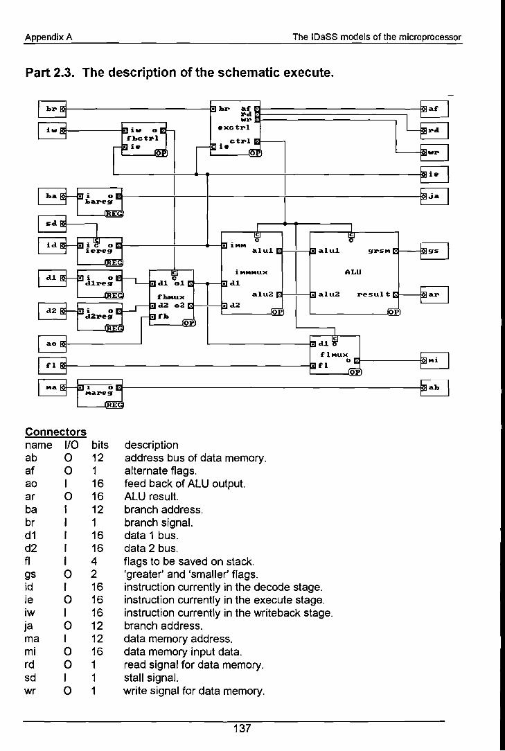
Appendix A The IDaSS models of the microprocessor
Part 2.3. The description of the schematic execute.
I bZO:: ;B: bzo af - ~af Izod
I iw~Wl/'_
zod. I:5:iw oEf- exctzol..,fbctzol tg. ctzol::
.- lEI ieroP
- C Ie mi~wzo IOP
~ie II I
~t.r.!j EJr sd lZj I .1 I
~ ~
I id '*- lEIi~ 0" ';'" iMM Cc
iezoeg - - aluJ.:: ::: al uJ. gZOSM :: b.. gS Ir'...J'REG
I d1.12j-\C~ iMMMUX iA LU
lEI i 013~ lEI dJ. coJ. = :::: dJ.dJ.zoeg
...J'REG alu2 :: ;:: al u2 zoesul t:: k. azo IfbMUX FI 12j-' ~IEId2 02::: ::: d2roP 'oPd2 • 1 0
!:Jd2ZOegl3 -lEIfb fMJïfE'( OP
I
I ao ~ ::: dJ. ~
IEl~
flMUXo
_ b.. Mi I':'fl ... r'~ roP
B-t~-l'J--------------------------iEJ
Connectorsname 1/0 bitsab 0 12at 0 1ao I 16ar 0 16ba I 12br I 1d1 I 16d2 I 16ti I 4gs 0 2id I 16ie 0 16iw I 16ja 0 12ma I 12mi 0 16rd 0 1sd I 1wr 0 1
descriptionaddress bus ot data memory.alternate tlags.teed back ot ALU output.ALU result.branch address.branch signa!.data 1 bus.data 2 bus.tlags to be saved on stack.'greater' and 'smaller' tlags.instruction currently in the decode stage.instruction currently in the execute stage.instruction currently in the writeback stage.branch address.data memory address.data memory input data.read signal tor data memory.stall signa!.write signal tor data memory.
137

Appendix A
Blocks
The IDaSS models of the microprocessor
ALU : operatorPurpose: Arithmetic Logic Unit; This block can perform 16 different arithmetic
operations. The following table shows the encoding of the functions of thisbloek.
This block also generates two flags. They form the output 'grsm' (greater and smaller).The input 'alu1' will always be compared with input 'alu2'. The coding ofthe signal 'grsm'is shown in the following tabel.
alü1=alu2alU1 >é11L/2 .alÜ1<alü2
Inputs: 'alu1', 16 bits; input 1 of the ALU.'alu2', 16 bits; input 2 ofthe ALU.'c', 7 bits, only bits 2,3,4 and 5 are used; the control connector.
Outputs: 'grsm', 2 bits; the flags 'greater' and 'smaller'.'result', 16 bits; the result of the arithmetic operation.
IDaSS description:
138

Appendix A The IDaSS models of the microprocessor
System-defined timing for this input 'c':Bus to command delay: 6n sec
System-defined timing for output 'grsm':Data transfer delay: 2n sec
System-defined timing for output 'result':Data transfer delay: 2n sec
System-defined output multiplexer delays:For output 'result': 7n sec
Text for function 'add':"Bé:l~ic add operation"... .. .
!!~~~1d~:~1i:~~roès) + (afÓ~, 1i~rdès) ..gr'sfrf;Ë(8/Û1·> aIÛ2),(alu1 <·8Iu2)
Internal time delays for function 'add':From 'alu1' to 'result': 14n secFrom 'alu2' to 'result': 14n secFrom 'alu1' to 'grsm': 11n secFrom 'alu2' to 'grsm': 11 n sec
Text for function 'and':l'B~sÎcàl1çfÓperàtion" .
Internal time delays for function 'and':From 'alu1' to 'result': 3n secFrom 'alu2' to 'result': 3n secFrom 'alu1' to 'grsm': 11 n secFrom 'alu2' to 'grsm': 11 n sec
139

Appendix A The IDaSS models of the microprocessor
Internal time delays for function 'cmp':From 'alu1' to 'grsm': 11 n secFrom 'alu2' to 'grsm': 11 n sec
Internal time delays for function 'epi':From 'alu1' to 'result': 2n secFrom 'alu1' to 'grsm': 11 n secFrom 'alu2' to 'grsm': 11 n sec
Text for function 'dec':"E3é1slcdecrement operatioh"
r~~~lt:::JaIÜ1,1ZerOeS)+ (160nès,rZ~"oes)<rrOm:1 to:f6. . .
gt~m:~(alu1> alu2),(alu1<aILl2)
Internal time delays for function 'dec':From 'alu1' to 'result': 14n secFrom 'alu1' to 'grsm': 11 n secFrom 'alu2' to 'grsm': 11 n sec
Text for function 'mhi':"rJl§\(~~§ltêl trom theinpÛtALU t. töthepyipLJt"
~llltr;~I~~'':~'d2):(::~1<.alu~;3i·Internal time delays for function 'mhi':
From 'alu1' to 'grsm': 11 n secFrom 'alu2' to 'grsm': 11 n sec
Text for function 'mov':"m9\jefdatêl frominpYt,ALÛ1........................................
...···.·.·.···.···.·.·.··l···t>(> ··.·.······1 ··>2reSLJ;= au.
140
Appendix A The IDaSS models of the microprocessor
l·grsm •••:#(ál.U·1··· ··;:.-····a lu21,·(ald1•••• <allj21•••• <>•• >•• >·.<>······ . ······························<.····.·••••u··>il
Internal time delays for function 'mov':From 'alu1' to 'grsm': 11 n secFrom 'alu2' to 'grsm': 11 n sec
Internal time delays for function 'or':From 'alu1' to 'result': 3n secFrom 'alu2' to 'result': 3n secFrom 'alu1' to 'grsm': 11 n secFrom 'alu2' to 'grsm': 11 n sec
"UHflry~eleçt seçond nible operatiön"Text for function 'seI2':
:<>:,.. <.: '::>::;::«<.:.:' :,,«::<.:.:.
j[ffflP:==äJurshr: 4.·rê$lJlt:S trllP l\%OOOOOOOÖ0000111J.§rsm:#:(álü1> àlu2),(aIU1 < alu2)
Internal time delays for function 'seI2':From '_tmp' to 'result': 3n secFrom 'alu1' to 'grsm': 11 n secFrom 'alu2' to 'grsm': 11 n sec
Text for function 'seI3':"Un~ryS~lëct third nible öperation'L
~f'i'!~~fJ+~hr'8. ..., ····i,;;i~'f)}i
.~;~~~:~(~~·df ••~~G02~~~~g1o~O~E~.~ •••1•••1••J••.••••.•.••••••••••.••••••••••••••••••.•••.•.............
Internal time delays for function 'seI3':From '_tmp' to 'result': 3n secFrom 'alu1' to 'grsm': 11 n secFrom 'alu2' to 'grsm': 11 n sec
Text for function 'set':"Unf:irysetöperation"<
Internal time delays for function 'set':
141

Appendix A The IDaSS models of the microprocessor
From 'alu1' to 'grsm': 11 n secFrom 'alu2' to 'grsm': 11 n sec
Text for function 'shI8':
Internal time delays for function 'shI8':From 'alu1' to 'grsm': 11 n secFrom 'alu2' to 'grsm': 11 n sec
Text for function 'shr':"UnarYsbiffright···opèfaHoh"« .
:-:.:-:::.:-:::::-:-:-..:.. ::-:.<::::::- :.. : .
i~~ult:==~IU1· shr:1·,grshl :=(älu1>alu2), (a1u1o<àlu2)
Internal time delays for function 'shr':From 'alu1' to 'grsm': 11 n secFrom 'alu2' to 'grsm': 11 n sec
Text for function 'shr8':"qnêrYshift right·over 8 bits operátióh'\
fg~8It:=áll.ltshr:·8.grsl'l1:~(áI1.l1 > alu2),(aluf<alu2) ..
Internal time delays for function 'shr8':From 'alu1' to 'grsm': 11 n secFrom 'alu2' to 'grsm': 11 n sec
Text for function 'sub':I "R~c:::;ii"'c",htr'o:l,,.t operation"
Internal time delays for function 'sub':From 'alu1' to 'result': 14n secFrom 'alu2' to 'result': 16n secFrom 'alu1' to 'grsm': 11 n secFrom 'alu2' to 'grsm': 11 n sec
Text for function 'xor':Il'sàSiêeXlusiveÖroperation"i>·< .
1<··<······IrésÜlf:=áILJ1 ·>.<àlu2>>
142

Appendix A
Internal time delays for function 'xor':From 'alu1' to 'result': 4n secFrom 'alu2' to 'result': 4n secFrom 'alu1' to 'grsm': 11 n secFrom 'alu2' to 'grsm': 11 n sec
The IDaSS modeIs of the microprocessor
bareg: registerPurpose: branch address register; This is the pipeline register for the branch address.
Inputs: 'i', 12 bits;Outputs: '0', 12 bits;
IDaSS description:
Default function: 'Ioad'Reset value: 4095 (OFFFh)System-defined timing for output '0':
Data transfer delay: 2n sec
System-defined timing for this register:Clock to data delay: Sn secClock to status delay: 7n secData setup time: 12n secCommand setup time: 7n sec
d1 reg: registerPurpose: data 1 register; This is the pipeline register for the data 1 bus.
Inputs: 'i', 16 bits.Outputs: '0', 16 bits.
IDaSS description:
Default function: 'Ioad'Reset value: 0
System-defined timing for output '0':Data transfer delay: 2n sec
System-defined timing for this register:Clock to data delay: Sn secClock to status delay: 7n secData setup time: 12n secCommand setup time: 7n sec
143

Appendix A The IDaSS models of the microprocessor
d2reg : registerPurpose: data 2 register; This is the pipeline register for the data 2 bus.
Inputs: 'i', 16 bits.Outputs: '0', 16 bits.
IDaSS description:
Default function: 'Ioad'Reset value: 0
System-defined timing for output '0':Data transfer delay: 2n sec
System-defined timing for this register:Clock to data delay: 8n secClock to status delay: 7n secData setup time: 12n secCommand setup time: 7n sec
exctrl : operatorPurpose: execute stage controller; This block is the instruction decoder for the execute
stage. It contrals the blocks ALU, flmux and immmux and also generates thecontro! signals for the data memory. The following table shows the severaltypes of instructions and the functions of the logic blocks for each of thosetypes. The readmem and wrifemem signals are the 'read' and 'write' controlsignals for the Data Memory. The a/tflag signa! is used in the Write-backstage and denotes that the flags may be altered by that instruction.Next to the instruction input 'ie' this logic block has another input. This is input'br'. This input will be 1 if a branch occurs. In those cases the Execute stagemust switch to a passive state. This is done by making all the control signalszero, except the read signalof the Data Memory which will be one.
144

Appendix A The IDaSS models of the microprocessor
···%OOOxxxxxxxxxxxxx.•·•••· ....!n8~X~.q.RiÓ~.r>' •••m9Y8B~.r~!i8n·~Q91_ ••••••••••9it~Ç[Rip~l"YmpY9P~t~tipQ.·.~q1.~i ••••imm~gi~~~RiQ~tX ••9R~t~li9Q$·.·· .•~lPqq~j@npiP$ttqctiQh..>
>%10ö1XXXXXXxxxxXX···· Jümpsû~t9ûtiJ)è.?>
%1chö_..••··· cönqiJiÖQ~ljump ....
.•...•..••..••..••.... oo.•..~o.11.•·.•....·.01..·...• ··••0101Xxxxxx··.·.·x·.·.·.x•• ·•· •.•xxx.··.··•• ·•·•· •.·.o···.·.xxxxxxxx..... oxxx· ..•... the djnziristruction,cthepöpTnstnjctiöH .~J1goXX}()Q<6xx1XXX>/thêpü$6iriStrÛêfiön··········· .}Yo1100)()()()QS1XXXXXX othërünarY9P~r~ti()ris·%l1b1)()()()öö()()() ..•••• reg. tbreg.Rin~rYtjperatiöns>~i1J)()()()()()<5<öooxxx . .•• tre fillipstrüçti6d .. .. .o~r11~q01xxx ··movet6IB8,DêRtj(SPR .%1j1~91 oxxx jUmp t(jihter[up(röqlihe%1f1~1XOXXXrefurnfrQmiritlsubroutirie
%111:>oöOööO<f11 xxx the nóinstructiörl>
note a) : bits 5..3 of instruction word ie.note b) : bit 3 of instruction word ie.note c) : inverted bit 3 of instruction word ie.note d) : ((ie from: 4 to: 5)-=%00),((ie from: 3 to: 5)=%001)
1·11 eX ç)
:•...••.1...•.:.:...:..:.••0•.1:.•.••.••..•.••..•l~~ .: •• ::••~iJ ~Il
•••• ,1 .·.iQ ... f>>6 <ff /iUp..••••. o. ··rf/011110>'·
.······.·.1. 11 ..•••..• () ..>11 ·11//1 >0
1·······11</011t1 /01>1/111.0
&>~l\~6•· ••• 0·. 11//0U 1.0··· 11>0>1
Inputs: 'br', 1 bit; the branch signa!.'ie', 16 bits; instruction in the execute stage, configured as a control connector.
Outputs: 'af, 1 bit; acontrol signal that denotes that the flags may be changed.'ctrl', 7 bits; the control word for the execute stage.'rd', 1 bit; the 'read' signal for the data memory.'wr', 1 bit; the 'write' signal for the data memory.
IDaSS description:
Control s ecification:
'~ê~Ç99~lb~Îhstrûçtiorl··.ld~6·•.Ë~hV91~ign~.!§il.. ••••••U••·.>i ·.L · .
•~b~~~~··."·'·hdèxed••••móvè"............................................................................. .
.·~lli~J.~••I.'Di.rect••••rT1ó~el,.................................................... .. ..•.•.••.•........ ..
·.I~~~ •••'II.~.k.~.~.iat; ••••~.~.~.rsti.~.~" •••••••••••••••••••••••••••••••••••••••••••••.•••••.•••.•.•••.••..••••.••••••.•.••.•.........••.•••...~1888~"Jümpql1~9riqi!iQb~l'i>····
.·]mp?? .••••.•••••>·.·.·.···········
145

Appendix A The IDaSS models of the microprocessor
System-defined timing for output 'af':Data transfer delay: 2n sec
System-defined timing for output 'ctrl':Data transfer delay: 2n sec
System-defined timing for control input 'ie':Bus to command delay: 6n sec
System-defined timing for output 'rd':Data transfer delay: 2n sec
System-defined timing for output 'wr':Data transfer delay: 2n sec
System-defined output multiplexer delays:For output 'af: 4n secFor output 'ctrl': 7n secFor output 'rd': 4n secFor output 'wr': 4n sec
146

Appendix A The IDaSS modeIs of the microprocessor
Internal time delays for function 'dir':From 'br' to 'ctrl': Sn secFrom 'ie' to 'ctrl': Sn secFrom 'br' to 'af: 2n secFrom 'br' to 'wr': Sn secFrom 'ie' to 'wr': Sn secFrom 'br' to 'rd': Sn secFrom 'ie' to 'rd': 7n sec
..." " .. "::.: .:.:-:.:.) :: .
',~émrÎ1lJ)ch();rnal" .·::AALL<UU?~h~2'têe"'i···« ..
. opera Ionli66rmálröüté·'
Internal time delays for function 'djnz':From 'br' to 'ctrl': Sn secFrom 'br' to 'af: 2n sec
147

Appendix A The IDaSS models of the microprocessor
Internal time delays for function 'fill':From 'br' to 'ctrl': Sn secFrom 'ie' to 'ctrl': Sn secFrom 'br' to 'af: 2n secFrom 'br' to 'wr': 2n sec
Internal time delays for function 'imm':From 'br' to 'ctrl': Sn secFrom 'ie' to 'ctrl': 13n secFrom 'br' to 'af: 2n sec
148

Appendix A The IDaSS models of the microprocessor
Internal time delays for function 'ind':From 'br' to 'ctrl': 5n secFrom 'ie' to 'ctrl': 5n secFrom 'br' to 'af: 2n secFrom 'br' to 'wr': 5n secFrom 'ie' to 'wr': 5n secFrom 'br' to 'rd': 5n secFrom 'ie' to 'rd': 7n sec
Text for function 'int':'P9rrypinterrupt subroutineoperation"· .....
1 ones, ....1 zeroes,
.. (ie from: 3 to: 5),20ries7:z:eroes,
Internal time delays for function 'int':From 'br' to 'ctrl': 5n secFrom 'ie' to 'ctrl': 5n secFrom 'br' to 'wr': 2n sec
149
Appendix A The IDaSS models of the microprocessor
Internal time delays for function 'je':From 'br' to 'ctrl': Sn secFrom 'ie' to 'ctrl': Sn sec
1 zeroes,
CU >i U•••.•.••••••••••••••••·•.•.1zeroes, ..(ie from:3to: 5),20nes7 zeroes.
Internal time delays for function 'jmp':From 'br' to 'ctrl': Sn secFrom 'ie' to 'ctrl': 5n sec
150

Appendix A
. "rnem write" ....................•..•..........•.................... . .
..•• ·:·:·:::)"ng~~~~é~&"·:· ..••.
Internal time delays for function 'jsr':From 'br' to 'ctrl': 5n secFrom 'ie' to 'ctrl': 5n secFrom 'br' to 'wr': 2n sec
"flags l"I'lay él1ter'i
Internal time delays for function 'movreg':From 'br' to 'ctrl': 5n secFrom 'ie' to 'ctrl': 5n secFrom 'br' to 'af: 2n sec
Text for function 'no ':"f'Jo Operätion: nothing may charge" ....
151
The IDaSS models of the microprocessor

Appendix A The IDaSS models of the microprocessor
Internal time delays for function 'pop':From 'br' to 'ctrl': Sn secFrom 'ie' to 'ctrl': Sn secFrom 'br' to 'af: 2n sec
Text for function' ush':."PLlsh óperation"
Internal time delays for function 'push':From 'br' to 'ctrl': Sn secFrom 'ie' to 'ctrl': Sn secFrom 'br' to 'af: 2n secFrom 'br' to 'wr': 2n sec
152
Appendix A The IDaSS models of the microprocessor
Internal time delays for function 'reg':From 'br' to 'ctrl': Sn secFrom 'ie' to 'ctrl': Sn secFrom 'br' to 'af: 2n sec
Internal time delays for function 'return':From 'br' to 'ctrl': Sn secFrom 'ie' to 'ctrl': Sn sec
Text for function 'uno ':"üther unary operations"
Internal time delays for function 'unop':From 'br' to 'ctrl': Sn secFrom 'ie' to 'ctrl': Sn secFrom 'br' to 'af: 2n sec
153
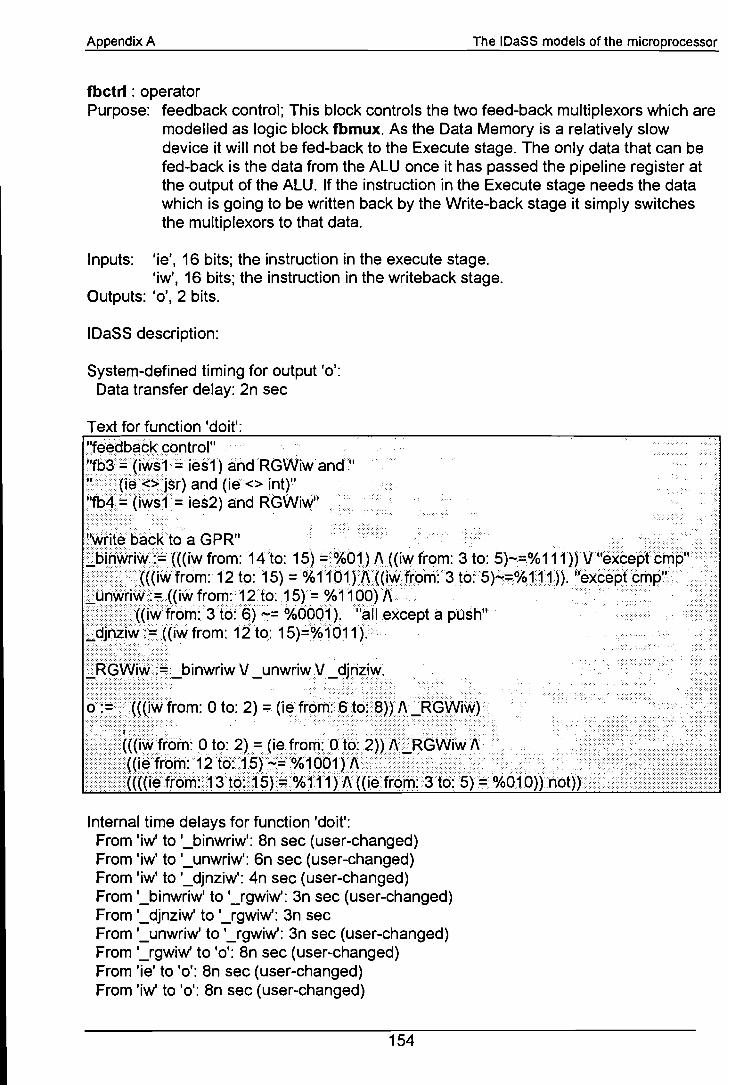
Appendix A The IDaSS models of the microprocessor
fbctrl : operatorPurpose: feedback control; This block contrals the two feed-back multiplexors which are
modelied as logic block fbrnux. As the Data Memory is a relatively slowdevice it will not be fed-back to the Execute stage. The only data that can befed-back is the data from the ALU once it has passed the pipeline register atthe output of the ALU. If the instruction in the Execute stage needs the datawhich is going to be written back by the Write-back stage it simply switchesthe multiplexors to that data.
Inputs: 'ie', 16 bits; the instruction in the execute stage.'iw' I 16 bits; the instruction in the writeback stage.
Outputs: '0', 2 bits.
IDaSS description:
System-defined timing for output '0':Data transfer delay: 2n sec
Text for function 'doit':
::::::::::::::::::::::::=::::::::::::::::::::::::::::::::::.-..... ".:
d::::«óWfrom: 0 to: 2) ={i~·•. fr()m:6to:t3))I\ __R<3VViwJnl.. .. .. . .....•.....··i> .•••.••••.•.. ...••..•••.•••.•.•.•••••.•.•.•...•. .... .... .«. ....>.>?••••••••
({(iWfról11: 0 to:2)=(i~frollJ:PJC);2))I\ __RGWiwl\>. . .. ...< .«(i~frc>[r1:1?t?:1pJHÊ%1991J~i>
. ((((ièfróHï:13tQ:1 t5)#%111 )1\ (( ieJrQHï:3 tö: 5):: %010Hnot)}
::::::::::::::::::::::~<:::::::::::;}:.. >.::::::::::;::::.
ÊRGv\IiW:#_binwriw V_unwriwV_djn?:hv.
"feedbáêk control""tb3=(hlv's1:::ièS1) áhdRGWiw and i'"(i~')~jsr)and (ie<> int)" ."fb4:::{iwsf= ies2) and RGWi'v\'f1
"wtit~backlo a GPR" .. . ... ... . . ......bifiwriW:= (((iw from:14to:15) =%Ö1)J\Ww from: 3 to: 5)-=%111))V"excepfêrnp"
i.·.····(((iwfrom:·12 to:··15) =%11ö1rÎ\((iWf~orn:3 to:5)4:;:%111})."èxcepfcrnp"Î.üI1Wriw:=r((iw from:J2lo:15)=%ftÖó)Jt· .
(iwfrórn:3tó:6)·~= %Ó001)~.i'áll .. except a push".2djhziw:§:((iw from: 12to: 15):::%1011).
Internal time delays for function 'doit':From 'iw' to '_binwriw': 8n sec (user-changed)From 'iw' to '_unwriw'; 6n sec (user-changed)From 'iw' to '_djnziw': 4n sec (user-changed)From '_binwriw' to '_rgwiw': 3n sec (user-changed)From '_djnziw' to '_rgwiw': 3n secFrom '_unwriw' to '_rgwiw': 3n sec (user-changed)From '_rgwiw' to '0': 8n sec (user-changed)From 'ie' to '0': 8n sec (user-changed)From 'iw' to '0': 8n sec (user-changed)
154
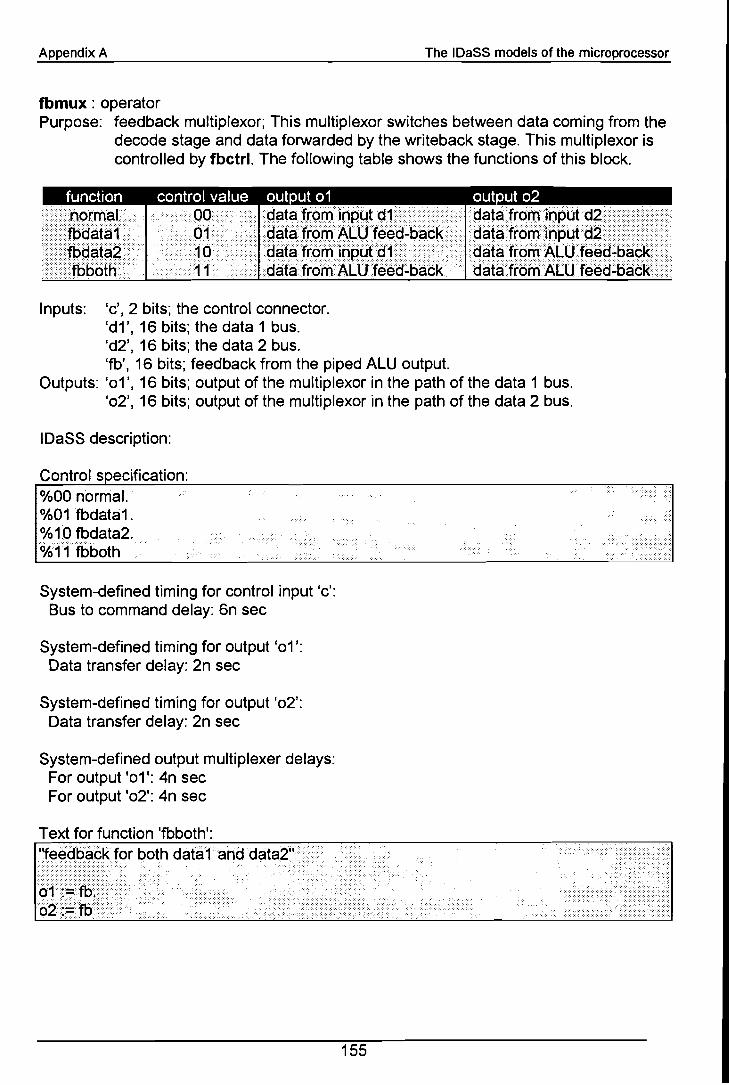
Appendix A The IDaSS models of the microprocessor
fbrnux : operatorPurpose: feedback multiplexor; This multiplexor switches between data coming from the
decode stage and data forwarded by the writeback stage. This multiplexor iscontrolled by fbctrl. The following table shows the functions of this block.
Inputs: 'c', 2 bits; the contro\ connector.'d1', 16 bits; the data 1 bus.'d2' I 16 bits; the data 2 bus.'fb', 16 bits; feedback from the piped ALU output.
Outputs: '01', 16 bits; output of the multiplexor in the path of the data 1 bus.'02', 16 bits; output of the multiplexor in the path of the data 2 bus.
IDaSS description:
Control s ecification:%00 normaL%01fbdata1.°/Ó1gn>data2.%11· fbboth
System-defined timing for control input 'c':Bus to command delay: 6n sec
System-defined timing for output '01':Data transfer delay: 2n sec
System-defined timing for output '02':Data transfer delay: 2n sec
System-defined output multiplexer delays:For output '01': 4n secFor output '02': 4n sec
Text for function 'fbboth':"feedbäck for both
155

Appendix A
Text for function 'fbdata1':
1''fè~dbai:Kf9f dálá1diîfy"
:~!!lili;~'Fi:,:ii"
The IDaSS models of the microprocessor
Text for function 'normal':
flmux: operatorPurpose: flag multiplexor; This block always passes the lower 12 bits of input d1. The
upper 4 bits can come from input d1 or from input fl. The latter will be selectedif the instruction is int. Switching is controlled by exctrl. The following tableshows the functions of this bloek.
Inputs: 'c' J 7 bits, only bit 6 is used; the control connector.'d1', 16 bits; the data 1 bus.'fl' J 4 bits; the flags from the writeback stage.
Outputs: '0', 16 bits; the data to be written to the data memory.
System-defined timing for contral input 'c':Bus to command delay: 6n sec
System-defined timing for this output:Data transfer delay: 2n sec
System-defined output multiplexer delays:For output '0': 4n sec
156

Appendix A
Text for function 'normal':.i'Wh~Qa~télWill·.be··WfittE3d•••tq•••m~rlib,yt' ••••••••••• •· •••• •·········· ...••~•••[.~ •••~.~ ••••••••••••••••.•••••••....•......
Text for function 'save':
The IDaSS models of the microprocessor
iereg : registerPurpose: This register will hold the instruction currently in the execute stage. It can be
'reset' by the stall signal 'sd'.
Inputs: 'c', 1 bits; the control connector.'i', 16 bits;
Outputs: '0', 16 bits;
IDaSS description:
Default function: 'Ioad'Reset value: 65535 (OFFFFh)Reset command value: 65535 (OFFFFh)
Control s ecification:•• 0'" ,. •
"onsfáll lead a NOP instruction".:.::::::::: ..:::;:; ..;.::.:::.::;::.... ::;:;:;:;:::;:;:;:;::::.
~ÓIB~d.·······
%fsétf6:$ffff
System-defined timing for this control input:Bus to command delay: 6n sec
System-defined timing for output '0':Data transfer delay: 2n sec
System-defined timing for this register:Clock to data delay: 8n secClock to status delay: 7n secData setup time: 12n secCommand setup time: 7n sec
157

Appendix A The IDaSS models of the microprocessor
immmux : operatorPurpose: immediate operations multiplexor; This block is the multiplexor that switches
between normal data feed-through or data modifications concerningimmediate data operations. This logic block contains two multiplexors that areswitched by two control signals from exctrl. The functions of this block areshown in the following tabie.
Inputs: 'c', 7 bits, only bits 0 and 1 are used; the control connector.'d1', 16 bits; the data 1 bus.'d2', 16 bits; the data 2 bus.'imm', 16 bits, only bits 6 .. 13 are used; the immediate value from the
instruction.Outputs: 'alu1', 16 bits; the first operand for the ALU.
'alu2', 16 bits; the second operand for the ALU.
IDaSS description:
Control s ecification:
System-defined timing for output 'alu1 ':Data transfer delay: 2n sec
System-defined timing for output 'alu2':Data transfer delay: 2n sec
System-defined timing for control input 'c':Bus to command delay: 6n sec
System-defined output multiplexer delays:For output 'alu1 ': 4n secFor output 'alu2': 4n sec
Text for function 'immhi h':
1l~~t§r9Ûtrr1gjncáseof an." ."i.rnrn~diat~m()Vê·t"Iigh···Opetêtion"·················
!igfIIglil!lib~:~i6: 13;,;§~f(6~:§i&i~'i;;l;j{i
158
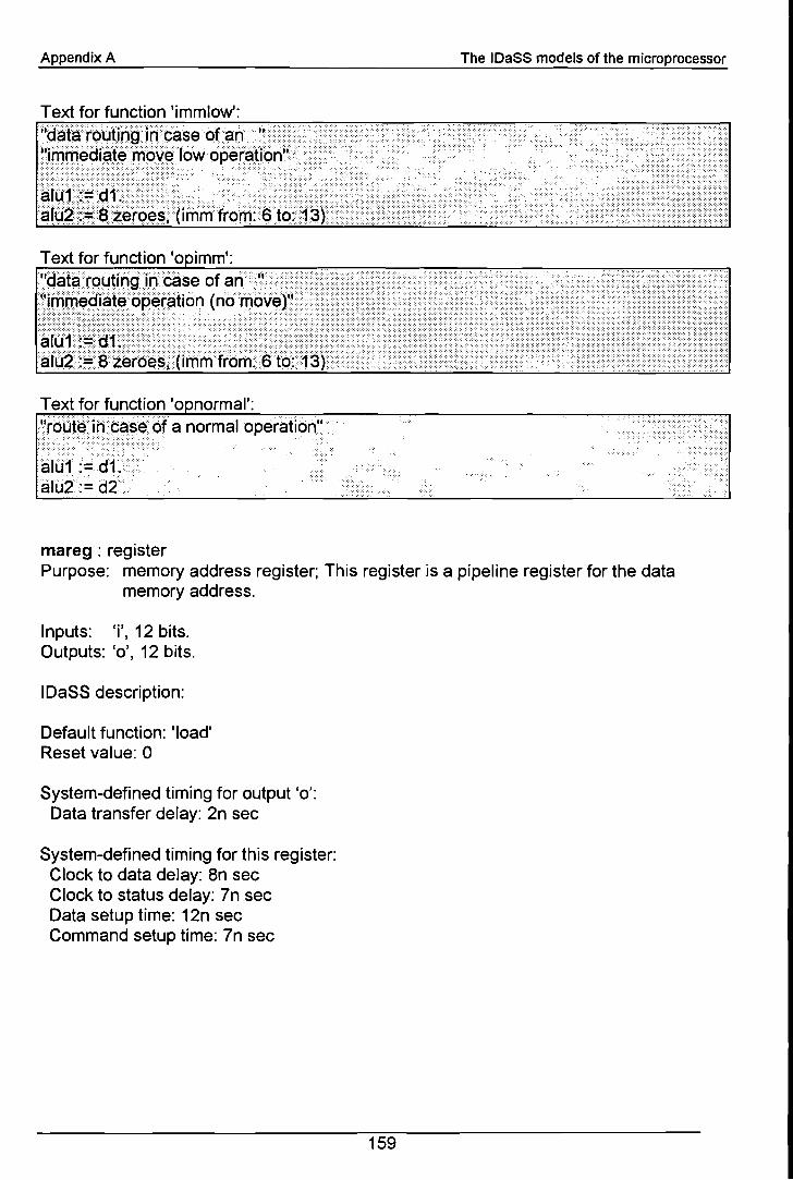
Appendix A
Text for function 'immlow':
The IDaSS models of the microprocessor
Text for function '0 normal':IIroÛt&JoP§$eOf a normal operation"<}::::\.<:~;.;~<.:-:::::><":~::::::::/:/<:::::::::::>:>
aIU1:=d1.... ·.älü2:= d2
mareg: registerPurpose: memory address register; This register is a pipeline register for the data
memory address.
Inputs: 'i', 12 bits.Outputs: '0', 12 bits.
IDaSS description:
Default function: 'Ioad'Reset value: 0
System-defined timing for output '0':Data transfer delay: 2n sec
System-defined timing for this register:Clock to data delay: 8n secClock to status delay: 7n secData setup time: 12n secCommand setup time: 7n sec
159

Appendix A The IDaSS models of the microprocessor
Part 2.4. The description of the schematic writeback.
IJa~~arej---__~La I
L[:Ji 0- b'- l I.. i''-1X"eg
-mEG
I gs ~ :E:i omI - l!JolclgsX"eg l!J gX"SM
JREG~;:: al t tlags m -
I at ~ ':"i omtlgen
....[:] MOatX"eg'""ao
JREG ~
- [!JiN e
I MO rrI Fc1rQPI
I aX" rrI ... o-I
~I ..:E:iN om -aX"X"egtletX"1
J'R"EGfOP
LtEltlI ie =' Ti 0-'.I.j '"'" ..
I-r, LX" IiNX"egLX" =e i'
rCJtR"EC' ... LX"logie.:.,IN
':" ao
I....
fOP
I ~iW Iba~ Ii'
Connectorsname 1/0 bitsaf I 1ao 0 16ar I 16ba 0 12br 0 1fl 0 4gs I 2ie I 16iw 0 16ja I 12mo I 16
descriptionif active this signal permits the flags to change.the piped output of the ALU.the direct output of the ALU.the piped branch address.the branch signa!.the flags.the 'greater' and 'smaller' flags.the instruction currently in the execute stage.the instruction currently in the writeback stage.the branch address.the output of the data memory.
160

Appendix A
Blacks
The IDaSS models of the microprocessor
afreg : registerPurpose: alternate flags register; This is the pipeline register for the signal that permits
logic block flgen to change the value of the flags.
Inputs: 'j' I 1 bit.Outputs: '0', 1 bit.
IDaSS description:
Default function: 'Ioad'Reset value: 0
System-defined timing for output '0':Data transfer delay: 2n sec
System-defined timing for this register:Cloek to data delay: 8n secClock to status delay: 7n secData setup time: 12n secCommand setup time: 7n sec
arreg : registerPurpose: ALU result register; This is the pipeline register for the ALU result.
Inputs: 'i', 16 bits.Outputs: '0', 16 bits.
IDaSS description:
Default function: 'Ioad'Reset value: 0
System-defined timing for output '0':Data transfer delay: 2n sec
System-defined timing for this register:Clock to data delay: 8n secClock to status delay: 7n secData setup time: 12n secCommand setup time: 7n sec
161

Appendix A The IDaSS models of the microprocessor
brlogic: operatorPurpose: branch logic; This block generates the 'br' signal (branch). If this signal is
active it indicates that all instructions in the pipeline must be flushed and thatthe branch address must be loaded by the Program Counter Register. Thebranch signal can only be activated by conditional branch instructions. Thefollowing table shows these instructions and the flag conditions on which thebranch signal must be activated.
instruction encoding flag conditions
1~~····i··ggg~·• ••••J'8.·.·.·. < .. ....../·.·jêl~.· ••.••.•••••••••••••••••••••••••••••.••••••..••.gg.~ .•~•.••••jêf ····0106~ge .. ... 9101JZ . 0110.·jnz 0111js· 1000'ns/ 1001
Inputs: 'ao', 16 bits; the piped output ofthe ALU.'fl', 4 bits; the flags.'iw', 16 bits; the instruction in the writeback stage.
Outputs: 'br', 1 bit; the branch signa!.
IDaSS description:
System-defined timing for output 'br':Data transfer delay: 2n sec
•••••~.6[~ ••~~ •••0~]~.1 ••••••••••••••••9~18~>abóVéptéqüäreqüàl<
·t·······················:·I····· .no equazer9nófierosetnotset
Text for function 'branch':'I;rhédqtpyfJndicates a.brarich tobetak~n"i>\:/iU:C::i/..··· :::<:/:"., :··:\::":··\::::::C ":::::"::.:' . :::>:"".. ::::.
L~t:.::((iwfröni: 12 tO:<15) = %101(»).êdjlÎz:§(nWftom:f2Jo:·15)=%1Qj1).< ...2.alün()tZ~r(): =(ao-=$OOOP). . .
162
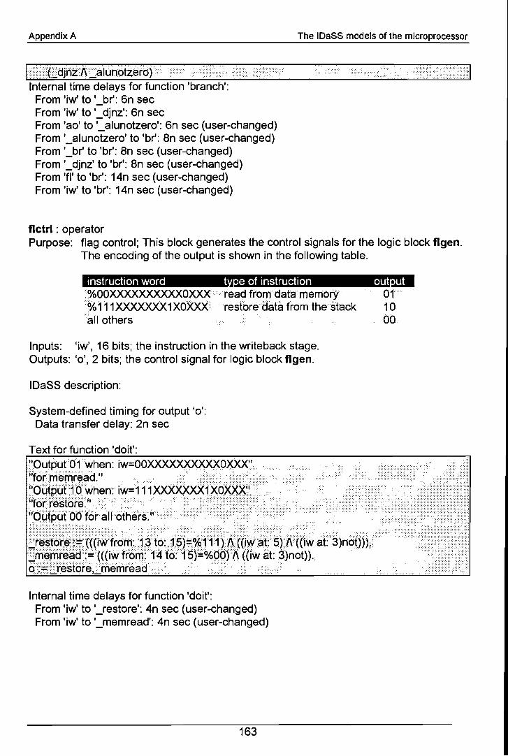
Appendix A The IDaSS models of the microprocessor
·...••••••• ?.••.••••••.••••••••••••••••••••••••••••••IInternal time delays for function 'branch':From 'iw' to '_br': 6n secFrom 'iw' to '_djnz': 6n secFrom 'ao' to '_alunotzero': 6n sec (user-changed)From '_alunotzero' to 'br': 8n sec (user-changed)From '_br' to 'br': 8n sec (user-changed)From '_djnz' to 'br': 8n sec (user-changed)From 'fl' to 'br': 14n sec (user-changed)From 'iw' to 'br': 14n sec (user-changed)
flctrl : operatorPurpose: flag control; This block generates the control signals for the logic block flgen.
The encoding of the output is shown in the following tabie.
instruction word t e of instruction out ut%OOXXXXXXXXXXOXXXread ffomdata memorY 01%111XXXXXXX1XOxxx. restÓrsdatà from theStack 10all others 00
Inputs: 'iw', 16 bits; the instruction in the writeback stage.Outputs: '0', 2 bits; the control signal for logic block flgen.
IDaSS description:
System-defined timing for output '0':
Data transfer delay: 2n sec
Text for function 'doit':"Outür01when: iw=OOXXXXXXXXXXOXXX""f6r~èrlîl'~ad." .. .>\u./1I0û!pqr~q'Nhen:iw=111 )()()ö()()ö(1Xq?Q9S'\
;:~~f;5:~6;6r~IIÓthêrs.ÎI<..>·
~~~~tg~~ ••••:.~ ••••((ti~·.·fro·m.: ...••1.3·.·.tÓ·:••••.1.S):o41···1·••1.·)..·d•••(.(.iw•••at:···.$)...."'...·(lW .at:·····S)not»).•••••••••·•••·•··•• .... < \mêrnr~à~:={((iW Hom:14l6:1s):f%Qö)i\ (OW àt:3)not)). . ........•..••..••••.•.•.••• ......j
ó;Ërrfêslofê,Lmemrêad ..... ...... .. .. .. . .
Internal time delays for function 'doit':From 'iw' to '_restore': 4n sec (user-changed)From 'iw' to '_memread': 4n sec (user-changed)
163

Appendix A The IDaSS models of the microprocessor
flgen : operatorPurpose: flag generator; This logic block determines the flags from the ALU and
memory outputs. There are 4 flag bits:flag bit 0: all zeroflag bit 1: all setflag bit 2: smallerflag bit 3: greater
This functions of this block are shown in the following tabie.
Inputs: 'alt', 1 bit; if this signal is active the flags are allowed to change.'ao', 16 bits; the piped output of the ALU.'c', 2 bits; the control connector.'grsm', 2 bits; the 'greater' and 'smaller' flags.'iw', 16 bits; the instruction in the writeback stage.'mo', 16 bits; the output of the data memory.'old', 4 bits; the flags generated by the former instruction.
Outputs: 'flags', 4 bits; the new flags.
IDaSS description.
Control s ecification:%PQ"feèdthrough Of flags".H.§rrTÎ~/... .. . . ..< . ...< •.. . .%01"détetniiheflagsfrorTl mèmreél9"reàdmèm. . ...•.. . .%lC)",.estqre flags from sfack
j; .•.
rêstdrè<
System-defined timing for control input 'c':Bus to command delay: 6n sec
System-defined timing for output 'flags':Data transfer delay: 2n sec
System-defined output multiplexer delays:For output 'flags': 4n sec
164
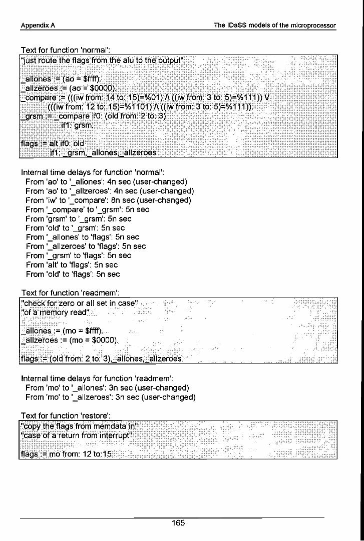
Appendix A The IDaSS models of the microprocessor
Internal time delays for function 'normal':From 'ao' to '_allones': 4n sec (user-changed)From 'ao' to '_allzeroes': 4n sec (user-changed)From 'iw' to '_compare': 8n sec (user-changed)From '_compare' to '_grsm': Sn secFrom 'grsm' to '_grsm': Sn secFrom 'old' to '_grsm': Sn secFrom '_allones' to 'flags': Sn secFrom '_allzeroes' to 'flags': Sn secFrom '_grsm' to 'flags': Sn secFrom 'alt' to 'flags': Sn secFrom 'old' to 'flags': Sn sec
Text for function 'readmem':"chécKforteroor all set in case'~ <;'6fi3mêm()ry rëad'.'< . .. . ......... .
=~IIOri~~:~(mo = ;ffff); ...•....:.àll:iêroes := (mo = $0000).
Internal time delays for function 'readmem':From 'mo' to '_allones': 3n sec (user-changed)From 'mo' to '_allzeroes': 3n sec (user-changed)
Text for function 'restore':"'ç9Pytb~fléJgsJr9m..•.._. ,.__.-"êásê6fafétûrn from
;I~~~:~~gfr~m: t~to:1$<
16S
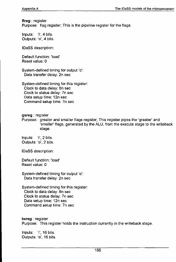
Appendix A The IDaSS models of the microprocessor
flreg : registerPurpose: flag register; This is the pipeline register for the flags.
Inputs: 'i', 4 bits.Outputs: '0', 4 bits.
IDaSS description:
Default function: 'Ioad'Reset value: 0
System-defined timing for output '0':Data transfer delay: 2n sec
System-defined timing for this register:Clock to data delay: 8n secClock to status delay: 7n secData setup time: 12n secCommand setup time: 7n sec
gsreg: registerPurpose: greater and smaller flags register; This register pipes the 'greater' and
'smaller' flags, generated by the ALU, from the execute stage to the writebackstage.
Inputs: 'j', 2 bits.Outputs: '0', 2 bits.
IDaSS description:
Default function: 'load'Reset value: 0
System-defined timing for output '0':Data transfer delay: 2n sec
System-defined timing for this register:Clock to data delay: 8n secClock to status delay: 7n secData setup time: 12n secCommand setup time: 7n sec
iwreg : registerPurpose: This register holds the instruction currently in the writeback stage.
Inputs: 'i', 16 bits.Outputs: '0', 16 bits.
166

Appendix A
IDaSS description:
Default function: 'Ioad'Reset value: 65535 (OFFFFh)
The IDaSS models of the microprocessor
System-defined timing for control input 'c':Bus to command delay: 6n sec
System-defined timing for output '0':Data transfer delay: 2n sec
System-defined timing for this register:Clock to data delay: 8n secClock to status delay: 7n secData setup time: 12n secCommand setup time: 7n sec
jareg : registerPurpose: This is the pipeline register for the branch address.
Inputs: 'j', 12 bits.Outputs: '0', 12 bits.
IDaSS description:
Default function: 'Ioad'Reset value: 4095 (OFFFh)
System-defined timing for output '0':Data transfer delay: 2n sec
System-defined timing for this register:Clock to data delay: 8n secClock to status delay: 7n secData setup time: 12n secCommand setup time: 7n sec
167

Appendix 8 The assembler code tor testing the instruction set
Appendix B.
The assembler code for testing the instruction set.0000: 8006 s~ar~up jmp s~ar~
0001: 80AC iD~s~r~ jmp iD~rou~
0002: ~
0002: 4054 ~es~jsr iDC r4 ~his is some code ~o
0003: D17C cmp r4,r5 ~es~ ~he jumpiDg from0004: D085 mov r5,r2 address 0000 ~o label0005: 1:030 r~s sur~.
0006: 4000 sur~ clr rO rO :- OOOOh0007: 43C8 mhi rO,Ofh rO :- OfOOh0008: 4441 mov r1,llh r1 :- OOllh0009: 4882 mov r2,22h r2 :- 0022hOOOA: 488A mhi r2,22h r2 :- 2222h0008: 4CC34CC8 movd r3,3333h r3 :- 3333hOOOD: DOC4 mov r4,r3 r4 :- 3333hOOOE: D085 mov r5,r2 r5 :- 2222hOOOF: D142 mov r2,r5 r2 :- 2222h0010: D046 mov r6,r1 r6 :- OOllh0011: D186 mov r6,r6 r6 :- OOllh0012: D007 mov r7,rO r7 :- OfOOh0013 : 1:04F mov bO,r7 bO :- fOOh0014: 1:24F mov b1,r7 b1 :- fOOh0015: E24E mov b1,r6 b1 :- Ollh0016: E44D mov b2,r5 b2 :- 222h0017 : E08D mov dO,r5 dO :- 222h0018: F08C mov d1,r4 dl :- 333h0019: E108 mov sp,r3 sp :- 333h001A: E10A mov sp,r2 sp :- 222h0018: 40004208 movd rO,0800h rO :- 0800h001D: 40014249 movd r1,0900h r1 :- 0900h001F: E088 mov dO,rO dO :- 800h0020: F089 mov d1,r1 dl :- 900h0021: 7F8243CA movd r2,Offeh r2 :- Offeh0023: E10A mov sp,r2 sp :- ffeh0024: 2409 mov dO[10h],r1 mem[810h] :- 0900h0025: 304A mov d1[01h],r2 mem[901h] :- Offeh0026: 2402 mov r2,dO[10h] r2 :- mem[810h]-0900h0027: 244A mov dO[llh] ,r2 mem[811h] :- 0900h0028: 0009 mov bO[rO],r1 mem[700h] :- 0900h0029: 0248 mov b1[r1],rO mem[911h] :- 0800h002A: 0007 mov r7, bO [rOl r7 :- mem[700h]-0900h0028: 004F mov bO[r1],r7 mem[800h] :- 0900h002C: 0046 mov r6,bO[r1] r6 :- mem[800h]-0900h002D: 0045 mov r5,bO[r1] ~ r5 :- mem[800h]-0900h002E: DOW ~es~ ~he o~her biDary opera~ioDs
002E: D010 add rO,rO rO :- 1000h002F: D1D5 add r5,r7 r5 :- 1200h0030: D157 add r7,r5 r7 :- 1bOOh0031: 4057 iDC r7 r7 :- 1b01h0032: 4057 add r7,l r7 :- 1b02h0033: 43E7 aDd r7,Ofh r7 :- 0002h0034: DOA5 aDd r5,r2 r5 :- OOOOh0035: D138 cmp r3,r4 equal0036: D038 cmp r3,rO grea~er
0037 : DOF8 cmp rO,r3 smaller0038: 407F cmp r7,Olh grea~er
0039: 408F cmp r7,02h equal003A: 40FF cmp r7,03h smaller0038: 7C2F or r7,OfOh r7 :- 00f2h003C: D028 or r3,rO r3 :- 3333h003D: D033 xor r3,rO r3 :- 2333h003E: 7FF4 xor r4,Offh r4 :- 33cch003F: DllF sub r7,r4 r7 :- cd26h0040: 405E dec r6 r6 :- 08ffh
169

Appendix B The assembler code tor testing the instruction set
0041: ;t.est.iIl9 of t.he fil! illst.ruct.ioll0041: 4004404C IDOvd r4,0100h r4 :- OlOOh0043: 4443444B mavd r3,llllh r3 :- lll1h0045: 43CS mav rS,Ofh rS :- OOOfh0046: ES4C mav b4,r4 b4 :- OlOOh0047: E943 fil! b4[rS],r3 ; mem[0100h •• 010fh] :- 1111h004S: ; t.est.iIl9 of t.he ullary operat.iolls004S: COOB push r30049: COOC push r4 ;swit.ch r3 alld r4004A: C003 pop r3 r3 :- 0100h004B: C004 pop r4 r4 :- lll1h004C: COS4 cpl r4 r4 :- eeeeh004D: COSD set. rS rS :- ffffh004E: 40SD dec rS rS :- fffeh004F: C06D shr rS r5 :- 7fffh0050: C075 shlS rS rS :- ffOOh0051: C07D shrS rS rS :- OOffh0052: 4D0444SC mavd r4,1234h r4 :- 1234h0054: 770S7FSD mavd rS,Ofedch rS :- fedch0056: C044 sel2 r4 r4 :- 0003h0057: C04D sel3 rS ; rS :- 001ehOOSS: ;t.est.iIl9 of t.he cOlldit.iollal braDch iDst.ruct.ioDS.OOSS: 4100 mav rO,40059: 4101 mav r1,4OOSA: 4102 IDOV r2,4OOSB: 40SS label1 dec rOOOSC: AFE7 jllz label1OOSD: 4100 mav rO,4OOSE: A026 label2 jz label3OOSF: 40SS dec rO0060: SOSE jmp label20061: 4059 label3 dec r10062: AFE9 jlls label30063: 4101 mav r1,40064: A02S label4 js labelS0065: 4059 dec r10066: S064 jmp label40067: 4050 labelS iDC rO006S: 4051 illc r10069: BFD2 djDz r2,labelS006A: A046 jz label7006B: 41CO label6 mav rO,7006C: 4101 mav r1,4006D: 41C2 mav r2,7006E: E030 rt.s006F: 9002 label7 jsr t.est.jsr0070: 4051 labelS iDC r10071: D039 cmp rl,rO0072: AFDO jbe labelS0073: 4051 illc r10074: 4050 label9 iDC rO0075: D039 cmp r1,rO0076: AFD3 jae label90077: 4059 lab10 dec r1007S: DOB9 cmp r1,r20079: AFDl ja lab10007A: 4051 labll iDC r1007B: D039 cmp rl,rO007C: AFD2 jb labll007D: 4059 lab12 dec rl007E: DOB9 cmp rl,r2007F: AFDS jlle lab12OOSO: D039 lab13 cmp rl,rOOOSl: A024 je lab1400S2: 4051 illc r100S3: SOSO jmp lab1300S4: 906B labl4 jsr label6ooss: 90S7 jsr lablS00S6: SOSA jmp lab1600S7: 4059 lab15 dec r1
170

Appendix B The assembler code tor testing the instruction set
OOSS: AFE7 jnz lab1S00S9: E030 rt.sOOSA: 90SC lab16 jsr lab17OOSB: S090 jmp lab19oosc: 40SA lab17 dec r2OOSD: A016 jz lab1SOOSE: 90SC jsr lab17OOSF: E030 lab1S rt.s0090: 4000 lab19 clr rO0091: 4001 clr r10092: D07S cmp rO,r10093: A04S jne lab200094: A03S jne lab200095: A02S jne lab200096: A014 je lab200097: 4001 clr r1009S: 4051 lab20 inc r10099: 4039 cmp r1,0009A: A014 je lab21009B: A004 je lab21009C: 43CS lab21 mov rS,Ofh009D: 4051 inc r1009E: 4000 clr rO009F: 403S cmp rO,OOOAO: A04S jne lab2200A1: D07S cmp rO,r100A2: E943 til! b4[rS],r300A3: 4000 clr rO00A4: 40C1 mov r1,3OOAS: 4050 lab22 inc rO00A6: D07S cmp rO,r100A7 : AOll ja lab23OOAS: SOAS jmp lab2200A9: 4040 lab23 mov rO,lOOAA: 4041 mov r1,1OOAB: S006 endlab jmp st.art.OOAC: ;OOAC: 4007 int.rout. clr r7OOAD: EE4F mov b7,r7OOAE: 407F cmp r7,1OOM: E020 rt.iOOBO:
SYMBOL TABLEENDLAB P OOab IN'rROUT P OOac IN'rSTRT P 0001 LAB10 P 0077
LABll P 007a LAB12 P 007d LAB13 P OOSO LAB14 P 0084LAB1S P 00S7 LAB16 P OOSa LAB17 P OOSc LAB1S P OOSfLAB19 P 0090 LAB20 P 009S LAB21 P 009c LAB22 P OOaSLAB23 P 00a9 LABEL1 P OOSb LABEL2 P OOSe LABEL3 P 0061
LABEL4 P 0064 LABELS P 0067 LABEL6 P 006b LABEL7 P 006fLABELS P 0070 LABEL9 P 0074 START P 0006 STARTUP P 0000
TESTJSR P 0002
171

Appendix C The assembler code of a realistic program
Appendix C.
The assembler code of a realistic program.This program was written by ir. L.C. Benschop to calculate the length/literals of a blockof data.
;freqtolen, compute code word lengths from frequency
belongs to pass 1 of bin sort.iszero mov b1[r2],r1
jmp pas1cont
;rO Number of symbols.;bO Address where frequencies reside.;b1 Address where lengths come.
mov r7,rOregisters.
movd r3,binheadsmov b2,r3movd r3,binlistmov b3,r3movd r3,bintailsmov b4,r3movd r3,binheads1mov b5,r3movd r3,binlist1mov b6,r3movd r3,sfreqsmov b7,r3movd r3,nclass
;Set length to zero for
;Direct page area.
;Initialize direct memory base
movd r1,Oa80hmov d1,r1 ;Initialize 1/0 base register.movd r3,freqsmov bO,r3movd r3,lengthsmov b1,r3movd rO,512jsr freqtolenmovd rO,512jsr lentocodejmp 4095
clr rOmov dO,rO
equ 0800hdorg OcOOhds 1024
dorg 0ds 64ds 16ds 0ds 32ds 16ds 32ds 32ds 512ds 512equ 0600h
initialize
sfreqs
; Memoryareas.directpgstackstaktopbinheadsbinheads1bintailsnclassbinlistbinlist1lengths
freqs
freqtolen; Set the base
0000:0000:0000:0040:0050:0050:0070:0080:OOAO:OOCO:02CO:0600:0000:0800:OCOO:OCOO:0000:0000: 40000001: E088register.0002: 600142890004: F0890005: 400342080007: E0480008: 40034188OOOA: E2480008: 40004088OOOD: 9014OOOE: 400040880010: 90D90011: 8FFF0012:0012:distribution.0012:0012 :0012 :0012 :0012:0012:0012: 02890013: 803Czero-freq0014:0014: D0070015:0015: 540340080017: E4480018: 70034008001A: E6480018: 60034008001D: E848001E: 5C0340080020: EA480021: 700340880023: EC480024: 400343080026: EE480027: 68034008
173

Appendix C The assembler code of a realistic program
0029: F04B mov b8,r3002A: C051: set r6002B: Prepare for pass 1 of the bin sort.002B: 43C2 mov r2,15002C: 1:486 fill b2[r2] ,r6 ;Set heads array.0020: 4001 clr r10021:: 4002 clr r2002F: 4004 clr r40030: 0083 pas1loop mov r3,bO[r2]0031: AE06 jz iszero0032: 4054 inc r40033: 431:3 and r3,150034: 04C5 mov r5,b2[r3]0035: A029 jns paslels0036: 04CA mov b2[r3] ,r20037: 803A jmp pas1endi0038: 08C5 paslels mov r5,b4[r3]0039: 074A mov b3[r5],r2003A: 08CA pas1endi mov b4[r3],r2003B: 0681: mov b3 [r2], r6003C: 4052 pas1cont inc r20030: 01FA cmp r2,r70031:: AF15 jne pas1loop003F: Prepare for pass 2 of the bin sort.003F: 43C2 mov r2,150040: I:A86 fill b5[r2] ,r6 ;Set binheads1 array.0041: 43C1 mov r1,150042: 0442 pas2loop mov r2,b2[r1]0043: AOC8 js pas2next0044: 0083 pas2inn mov r3,bO[r2]0045: C043 se12 r30046: OAC5 mov r5,b5[r3]0047: A029 jns pas2else0048: OACA mov b5 [r3], r20049: 804C jmp pas2endi004A: 08C5 pas2else mov r5,b4[r3]004B: 004A mov b6[r5],r2004C: 08CA pas2endi mov b4[r3],r20040: OC81: mov b6[r2],r60041:: 0682 mov r2 ,b3 [r2]004F: AF49 jns pas2inn0050: 4059 pas2next dec r10051: AF09 jns pas2loop0052: ; Prepare for pass 3 of the bin sort.0052: 47C2 mov r2,310053: 1:486 till b2 [r2], r6 ;Set binheads array.0054: 43C1 mov r1,150055: OA42 pas3loop mov r2,b5[r1]0056: AOC8 js pas3next0057: 0083 pas3inn mov r3,bO[r2]0058: C04B se13 r30059: 04C5 mov r5,b2[r3]005A: A029 jns pas3else005B: 04CA mov b2 [r3], r2005C: 805F jmp pas3endi0050: 08C5 pas3else mov r5,b4[r3]0051:: 074A mov b3[r5],r2005F: 08CA pas3endi mov b4[r3],r20060: 0681: mov b3[r2],r60061: OC82 mov r2,b6[r2]0062: AF49 jns pas3inn0063: 4059 pas3next dec r10064: AF09 jns pas3loop0065: ; Bin sort done. Place sorted frequencies in sfreqs array.0065: 4002 clr r20066: 47C1 mov r1,3l0067: 0443 wsortloop mov r3,b2 [rl]0068: A058 js wsortnext0069: 00C5 wsortinn mov r5,bO[r3]006A: 01:80 mov b7[r2],r5
174
Appendix C The assembler code of a realistic program
006B: .052 iDC r2006C: 06C3 mov r3,b3[r3]006D: AFB9 jDs wsort:iDD006E: .059 wsort:Dext: dec r1006F: AF79 JDS wsort:loop0070: Now ready for t:he Lu/CheD Algorit:hm0070: CODt:ract:ioD St:age.0070: i-rl Ip-r2 m-r30070: t:ot:-r. aux-rS0070: .041 mov r1,10071: D102 mov r2,r.0072: .ODA sub r2,30073 : .003 clr r3007.: D106 mov r6,r.0075: .OSE dec r60076: OF8S mov rS,b7[r6]0077: .OSE dec r60078: OF86 mov r6,b7[r6]0079: D19S add rS,r6007A: OE86 cODt:rloop mov r6,b7[r2]007B: D1BD cmp rS,r6007C: AOA2 jb cODt:relse007D: OE80 mov rO,b7[r2]007E: D086 mov r6,r2007F: DU6 add r6,r.0080: DOSE sub r6,r10081: .09E sub r6,20082: OF88 mov b7[r6],rO0083: .053 iDC r3008.: .OSA dec r20085: A1E8 js cODt:reDd0086: 807A jmp cODt:rloop0087 : D086 cODt:relse mov r6,r20088: DU6 add r6,r.0089: DOSE sub r6,r1008A: .09E sub r6,2008B: OF8D mov b7 [r6], rS008C: OC.B mov b6[r1],r3008D: .051 iDC r1008E: D106 mov r6,r.008F: .09E sub r6,20090: D1B9 cmp r1,r60091: A12. je cODt:reDd0092: D106 mov r6,r.0093: DOSE sub r6,r1009.: .OSE dec r60095: D1BA cmp r2,r60096: A06S jDe cODt:2else0097: OE8S mov rS,b7[r2]0098: D196 shl r60099: OF86 mov r6,b7[r6]009A: D19S add rS,r6009B: .OSA dec r2009C: 807A jmp cODt:rloop009D: D196 cODt:2else shl r6009E: OF8S mov rS,b7[r6]009F: .OSE dec r6OOAO: OF86 mov r6,b7[r6]00A1: D19S add rS,r600A2: .OSB dec r300A3: 807A jmp cODt:rloopOOA.: D10S CODt:reDd mov rS,r.OOAS: .09D sub rS,200A6: 80AA jmp cODt:2Dext:00A7: OC.B CODt:21oop mov b6[r1],r300A8: .OSB dec r300A9: .051 iDC r1OOAA: D179 cODt:2Dext: cmp r1,rSOOAB: AFB2 jb cODt:2loopOOAC: ~ Next: t:he expaDsioD st:age.
175

Appendix C The assembler code of a realistic program
;LeDtocode Compute caDoDical HuffmaD codes from leDgths.;b1 poiDts to array of code word leDgths, b7 POiDts to area;where code words are stored, rO is Dumher of code words.leDtocode mov r7,rO
set r6; First Pass: collect the code word leDgths iD each iD their OWD
OOAC:OOAC: 4042OOAD: 108AOOAE: 4052OOAF: 108A0080: 40830081: D1010082: 40D90083: A1460084: 10850085: OC460086: D17E0087: A0630088: 10860089: 405EOOBA: 108E0088: 4052OOBC: 1088008D: 80C6008E: D085008F: 405DOOCO: 114600C1: 4051:00C2: 114E00C3: 108600C4: 409600C5: 108E00C6: 405900C7: AEC700C8:00C8: 404300C9: lOCSOOCA: 47C100C8: 0442OOCC: A098OOCD: 403DOOCE: A035OOCF: 4053OODO: lOCS00D1: AFD600D2: 028800D3: 405D00D4: 068200D5: AF7900D6: 405900D7: AF3900D8: E03000D9:00D9:00D9:00D9:00D9: D007OODA: C05E00D8:biD.00D8: 4442OODC: E486OODD: 4002OODE: 0283OODF: A086OOEO: 04C400E1: A02900E2: 04CA00E3: 80E600E4: 08C400E5: 070A00E6: 08CA00E7: 068E00E8: 405200E9: D1FA
exploop
expelse
expeDdi
;FiDallyexpeDd
IgeDloop
IgeDiDD
IgeDwhile
IgeDeDdwh
IgeDcoDt
ltclloop
ltclelse
ItcleDdi
ItclcoDt
mov r2,lmov b8[r2],r2iDC r2mov b8[r2],r2mov r3,2mov rl,r4sub rl,3jz expeDdmov r5,b8[r2]mov r6,b6[rl]cmp r6,r5jae expelsemov r6,b8[r2]dec r6mov b8[r2],r6iDC r2mov b8 [r2] , r3jmp expeDdimov r5,r2dec r5mov r6,b8[r5]dec r6mov b8[r5],r6mov r6,b8[r2]add r6,2mov b8[r2],r6dec r1jDZ exploop
geDerate the code wordmov r3,lmov r5,b8[r3]mov rl,3lmov r2,b2 [rl]js IgeDcoDtcmp r5,0jDe IgeDeDdwhiDC r3mov r5,b8[r3]jz IgeDwhilemov bl [r2] , r3dec r5mov r2,b3[r2]jDs IgeDiDDdec rlJDS IgeDlooprts
mov r2,l7till b2[r2],r6clr r2mov r3,bl[r2]jz ItclcoDtmov r4,b2[r3]JDS Itc1elsemov b2[r3],r2jmp ItcleDdimov r4,b4[r3]mov b3[r4],r2mov b4[r3],r2mov b3[r2],r6iDC r2cmp r2,r7
leDgths.
176

Appendix C
OOEA: AF35OOEB:OOEB: "00"600COOED: "005OOEE: "042OOEF: ""OlOOFO: 0"S300F1: AO"S00F2: OECD00F3: D1l5OOF": 06C300F5: AFC900F6: C06C00F7: "052OOFS: "05900F9: AF67OOFA: E030OOFB:
The assembler code of a realistic program
jlle lt.elloopSeeolld Pass: Assigll code words t.o illereasillg lellgt.hs.
movd r4,SOOOhelr r5mov r2,1mov rl,16
lt.e21oop mov r3,h2[r2]js lt.e2eollt.
lt.e2illll mov h7[r3],r5add r5,r4mov r3,h3[r3]jlls lt.e2illll
lt.e2eollt. shr r"ille r2dec rljllz lt.e21ooprt.s
SYMBOL TABLEBINHEADS D 0050 BINHEADSl D 0070 BINLIST D OOeO BINLISTl D 02eOBINTAILS D OOSO CONT2ELSE P 009d CONT2LOOP P 00a7 CONT2NEXT P OOaa
CONTRELSE P 00S7 CONTREND P OOa" CONTRLOOP P 007a DlRECTPG D 0000EXPELSE P OOhe EXPEND P OOeS EXPENDI P 00e6 EXPLOOP P 00h4
FREQS C OSOO FREQTOLEN P 0014INITIALIZE P 0000 ISZERO P 0012LENGTHS C 0600 LENTOCODE P 00d9 LGENCONT P 00d6 LGENENDWH P 00d2LGENINN P OOed LGENLOOP P OOeh LGENWHILE P OOef LTC1CONT P OOeS
LTC1ELSE P 00e4 LTC1ENDI P 00e6 LTC1LOOP P OOde LTC2CONT P 00f6LTC2INN P 00f2 LTC2LOOP P OOfO NCLASS D OOaO PAS1CONT P 003ePASlELS P 003S PAS1ENDI P 003a PAS1LOOP P 0030 PAS2ELSE P 004a
PAS2ENDI P 004e PAS2INN P 0044 PAS2LOOP P 0042 PAS2NEXT P 0050PAS3ELSE P 005d PAS3ENDI P 005f PAS3INN P 0057 PAS3LOOP P 0055PAS3NEXT P 0063 SFREQS D OeOO STACK D 0040 STAKTOP D 0050WSORTINN P 0069 WSORTLOOP P 0067 WSORTNEXT P 006e
177