tibpal20l8-15c, tibpal20r4-15c, tibpal20r6-15c, …
TRANSCRIPT
TIBPAL20L8-15C, TIBPAL20R4-15C, TIBPAL20R6-15C, TIBPAL20R8-15CTIBPAL20L8-20M, TIBPAL20R4-20M, TIBPAL20R6-20M, TIBPAL20R8-20M
HIGH-PERFORMANCE IMPACT�™ PAL® CIRCUITSSRPS021A − D2920, JUNE 1986 − REVISED DECEMBER 2010
POST OFFICE BOX 655303 • DALLAS, TEXAS 75265
Copyright © 2010, Texas Instruments Incorporated
1
PRODUCTION DATA information is current as of publication date.Products conform to specifications per the terms of Texas Instrumentsstandard warranty. Production processing does not necessarilyinclude testing of all parameters.
• High-Performance: fmax (w/o feedback)TIBPAL20R’ -15C Series . . . 45 MHzTIBPAL20R’ -20M Series . . . 41.6 MHz
• High-Performance . . . 45 MHz Min
• Reduced ICC of 180 mA Max
• Functionally Equivalent, but Faster ThanPAL20L8, PAL20R4, PAL20R6, PAL20R8
• Power-Up Clear on Registered Devices (AllRegister Outputs are Set Low, but VoltageLevels at the Output Pins Go High)
• Preload Capability on Output RegistersSimplifies Testing
• Package Options Include Both Plastic andCeramic Chip Carriers in Addition to Plasticand Ceramic DIPs
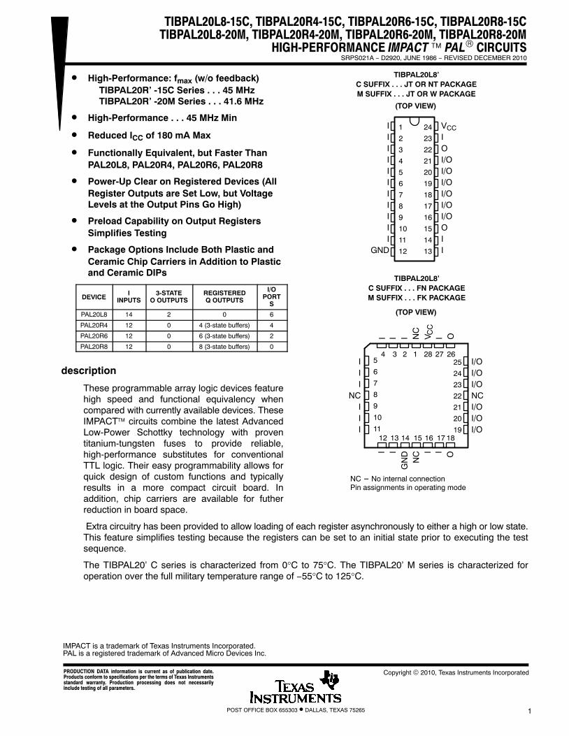
DEVICEI
INPUTS3-STATE
O OUTPUTSREGISTEREDQ OUTPUTS
I/OPORT
S
PAL20L8 14 2 0 6
PAL20R4 12 0 4 (3-state buffers) 4
PAL20R6 12 0 6 (3-state buffers) 2
PAL20R8 12 0 8 (3-state buffers) 0
description
These programmable array logic devices featurehigh speed and functional equivalency whencompared with currently available devices. TheseIMPACT™ circuits combine the latest AdvancedLow-Power Schottky technology with proventitanium-tungsten fuses to provide reliable,high-performance substitutes for conventionalTTL logic. Their easy programmability allows forquick design of custom functions and typicallyresults in a more compact circuit board. Inaddition, chip carriers are available for futherreduction in board space.
Extra circuitry has been provided to allow loading of each register asynchronously to either a high or low state.This feature simplifies testing because the registers can be set to an initial state prior to executing the testsequence.
The TIBPAL20’ C series is characterized from 0°C to 75°C. The TIBPAL20’ M series is characterized foroperation over the full military temperature range of −55°C to 125°C.
IMPACT is a trademark of Texas Instruments Incorporated.PAL is a registered trademark of Advanced Micro Devices Inc.
1
2
3
4
5
6
7
8
9
10
11
12
24
23
22
21
20
19
18
17
16
15
14
13
IIIIIIIIIII
GND
VCCIOI/OI/OI/OI/OI/OI/OOII
TIBPAL20L8’C SUFFIX . . . JT OR NT PACKAGEM SUFFIX . . . JT OR W PACKAGE
(TOP VIEW)
3 2 1 28 27
12 13
5
6
7
8
9
10
11
25
24
23
22
21
20
19
I/OI/OI/ONCI/OI/OI/O
III
NCIII
4 26
14 15 16 17 18
I IG
ND
NC I I O
I I I NC
I O
TIBPAL20L8’C SUFFIX . . . FN PACKAGEM SUFFIX . . . FK PACKAGE
(TOP VIEW)
NC − No internal connectionPin assignments in operating mode
V CC
TIBPAL20R4-15C, TIBPAL20R6-15C, TIBPAL20R8-15CTIBPAL20R4-20M, TIBPAL20R6-20M, TIBPAL20R8-20MHIGH-PERFORMANCE IMPACT�™ PAL® CIRCUITSSRPS021A − D2920, JUNE 1986 − REVISED DECEMBER 2010
POST OFFICE BOX 655303 • DALLAS, TEXAS 752652
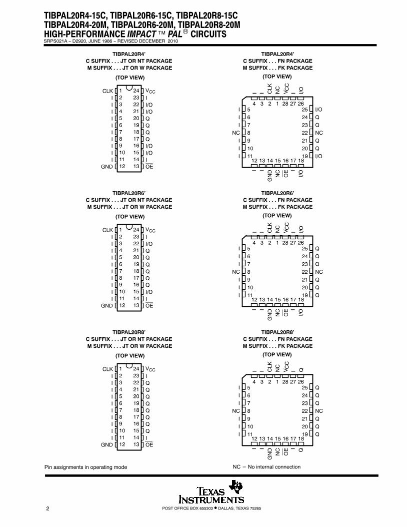
CLKIIIIIIIIII
GND
II/OI/OQQQQI/OI/OI
123456789101112
242322212019181716151413
VCC
OE
TIBPAL20R4’C SUFFIX . . . JT OR NT PACKAGE M SUFFIX . . . JT OR W PACKAGE
(TOP VIEW)
I I
GN
D
NC I
I/O
I I CLK
NC
I I/O
(TOP VIEW)
V CC
11 1912 13 14 15 16 17 18
4
10
9
8
7
6
5 I/O
20
21
22
23
24
253 2 1 28 27 26
I
I
I
NC
I
I
I
Q
Q
NC
Q
Q
I/O
TIBPAL20R4’C SUFFIX . . . FN PACKAGEM SUFFIX . . . FK PACKAGE
NC − No internal connection
OE
CLKIIIIIIIIII
GND
II/OQQQQQQI/OI
123456789101112
242322212019181716151413 OE I I
GN
D
NC I
I/O
I I CLK
NC
I I/OV CC
11 1912 13 14 15 16 17 18
4
10
9
8
7
6
5 Q
20
21
22
23
24
253 2 1 28 27 26
I
I
I
NC
I
I
I
Q
Q
NC
Q
Q
Q
OE
VCC
(TOP VIEW)
TIBPAL20R6’C SUFFIX . . . JT OR NT PACKAGE M SUFFIX . . . JT OR W PACKAGE
(TOP VIEW)
TIBPAL20R6’C SUFFIX . . . FN PACKAGEM SUFFIX . . . FK PACKAGE
CLKIIIIIIIIII
GND
IQQQQQQQQI
123456789101112
242322212019181716151413 OE I I
GN
D
NC I Q
I I CLK
NC
I QV CC
11 1912 13 14 15 16 17 18
4
10
9
8
7
6
5 Q
20
21
22
23
24
253 2 1 28 27 26
I
I
I
NC
I
I
I
Q
Q
NC
Q
Q
Q
OE
VCC
(TOP VIEW)
TIBPAL20R8’C SUFFIX . . . JT OR NT PACKAGE M SUFFIX . . . JT OR W PACKAGE
(TOP VIEW)
TIBPAL20R8’C SUFFIX . . . FN PACKAGEM SUFFIX . . . FK PACKAGE
Pin assignments in operating mode
TIBPAL20L8-15C, TIBPAL20R4-15CTIBPAL20L8-20M, TIBPAL20R4-20M
HIGH-PERFORMANCE IMPACT�™ PAL® CIRCUITSSRPS021A − D2920, JUNE 1986 − REVISED DECEMBER 2010
POST OFFICE BOX 655303 • DALLAS, TEXAS 75265 3
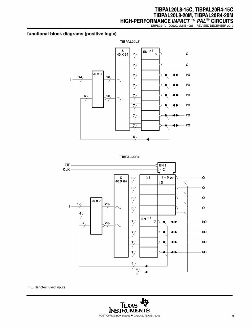
functional block diagrams (positive logic)
O
O
I/O
I/O
I/O
I/O
I/O
I/O
I
EN ≥1&40 X 64
14 20
206
7
7
7
7
7
7
7
7
6
20 x
denotes fused inputs
Q
I/O
I/O
I/O
I/O
I
EN
12 20
204
7
7
7
8
8
8
7
4
20 x
≥1
&40 X 64
≥1
8
Q
Q
Q
4
1D
I = 0 2
CLK C1EN 2OE
4
TIBPAL20L8’
TIBPAL20R4’

TIBPAL20R6-15C, TIBPAL20R8-15CTIBPAL20R6-20M, TIBPAL20R8-20MHIGH-PERFORMANCE IMPACT�™ PAL® CIRCUITSSRPS021A − D2920, JUNE 1986 − REVISED DECEMBER 2010
POST OFFICE BOX 655303 • DALLAS, TEXAS 752654
functional block diagrams (positive logic)
denotes fused inputs
TIBPAL20R6’
TIBPAL20R8’
Q
I/O
I/O
I
EN
12 20
202
7
8
8
8
7
2
20 x
≥1
&40 X 64
≥1
8
Q
Q
Q
6
1D
I = 0 2
CLK C1EN 2OE
6
8 Q
8 Q
Q
I12 20
208
8
8
8
8
20 x
8
Q
Q
Q
1D
I = 0 2
CLK C1EN 2
8 Q
8 Q
&40 X 64
≥1
OE
8 Q
8 Q
4 8 12 16 20 24 28 32
I3
I4
I5
I6
I7
I8
I9
I10
O22
I/O21
I/O20
I/O19
I/O18
I/O17
I/O16
O15
I14
IncrementI
1
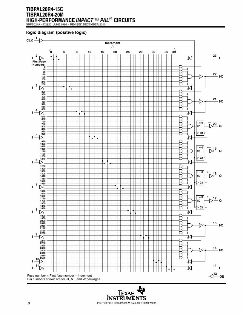
Fuse number = First fuse number + IncrementPin numbers shown are for JT, NT, and W packages.
04080
120160200240280
320360400440480520560600
640680720760800840880920
9601000104010801120116012001240
12801320136014001440148015201560
16001640168017201760180018401880
19201960200020402080212021602200
22402280232023602400244024802520
First FuseNumbers
36 390
I2
I23
I11
I13
TIBPAL20L8-15CTIBPAL20L8-20M
HIGH-PERFORMANCE IMPACT�™ PAL® CIRCUITSSRPS021A − D2920, JUNE 1986 − REVISED DECEMBER 2010
POST OFFICE BOX 655303 • DALLAS, TEXAS 75265 5
logic diagram (positive logic)
Fuse number = First fuse number + IncrementPin numbers shown are for JT, NT, and W packages.
4 8 12 16 20 24 28 32
I3
I4
I5
I6
I7
I8
I9
I10
I/O22
I/O21
I/O16
I/O15
Increment
04080
120160200240280
320360400440480520560600
640680720760800840880920
9601000104010801120116012001240
12801320136014001440148015201560
16001640168017201760180018401880
19201960200020402080212021602200
22402280232023602400244024802520
First FuseNumbers
36 390
I2
I23
I11
I14
Q20
Q19
Q18
Q17
C1
1DI = 0
C1
1DI = 0
C1
1DI = 0
C1
1DI = 0
13OE
CLK1
TIBPAL20R4-15CTIBPAL20R4-20MHIGH-PERFORMANCE IMPACT�™ PAL® CIRCUITSSRPS021A − D2920, JUNE 1986 − REVISED DECEMBER 2010
POST OFFICE BOX 655303 • DALLAS, TEXAS 752656
logic diagram (positive logic)

Fuse number = First fuse number + IncrementPin numbers shown are for JT, NT, and W packages.
4 8 12 16 20 24 28 32
I3
I4
I5
I6
I7
I8
I9
I10
I/O22
I/O15
Increment
04080
120160200240280
320360400440480520560600
640680720760800840880920
9601000104010801120116012001240
12801320136014001440148015201560
16001640168017201760180018401880
19201960200020402080212021602200
22402280232023602400244024802520
First FuseNumbers
36 390
I2
I23
I11
I14
Q20
Q19
Q18
Q17
C1
1DI = 0
C1
1DI = 0
C1
1DI = 0
C1
1DI = 0
13OE
CLK1
Q21
C1
1DI = 0
Q16
C1
1DI = 0
TIBPAL20R6-15CTIBPAL20R6-20M
HIGH-PERFORMANCE IMPACT�™ PAL® CIRCUITSSRPS021A − D2920, JUNE 1986 − REVISED DECEMBER 2010
POST OFFICE BOX 655303 • DALLAS, TEXAS 75265 7
logic diagram (positive logic)
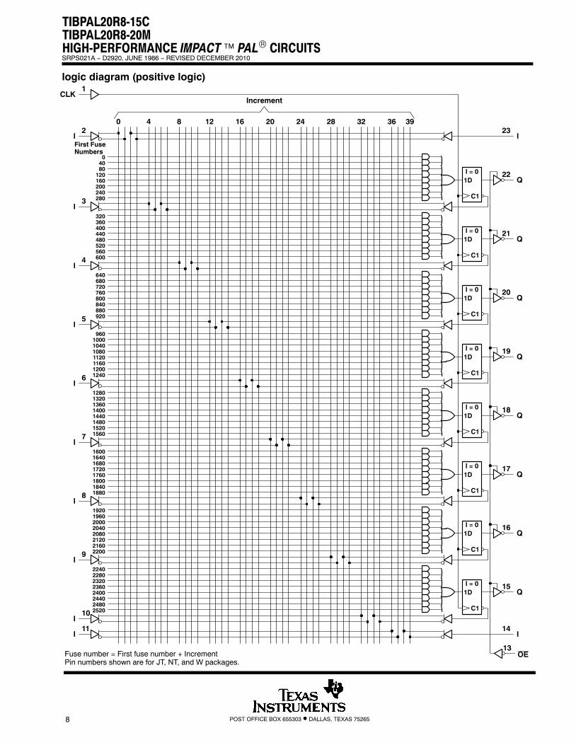
Fuse number = First fuse number + IncrementPin numbers shown are for JT, NT, and W packages.
4 8 12 16 20 24 28 32
I3
I4
I5
I6
I7
I8
I9
I10
Increment
04080
120160200240280
320360400440480520560600
640680720760800840880920
9601000104010801120116012001240
12801320136014001440148015201560
16001640168017201760180018401880
19201960200020402080212021602200
22402280232023602400244024802520
First FuseNumbers
36 390
I2
I23
I11
I14
Q20
Q19
Q18
Q17
C1
1DI = 0
C1
1DI = 0
C1
1DI = 0
C1
1DI = 0
13OE
CLK1
Q21
C1
1DI = 0
Q16
C1
1DI = 0
Q22
C1
1DI = 0
Q15
C1
1DI = 0
TIBPAL20R8-15CTIBPAL20R8-20MHIGH-PERFORMANCE IMPACT�™ PAL® CIRCUITSSRPS021A − D2920, JUNE 1986 − REVISED DECEMBER 2010
POST OFFICE BOX 655303 • DALLAS, TEXAS 752658
logic diagram (positive logic)
TIBPAL20L8-15C, TIBPAL20R4-15C, TIBPAL20R6-15C, TIBPAL20R8-15CHIGH-PERFORMANCE IMPACT�™ PAL® CIRCUITS
SRPS021A − D2920, JUNE 1986 − REVISED DECEMBER 2010
POST OFFICE BOX 655303 • DALLAS, TEXAS 75265 9
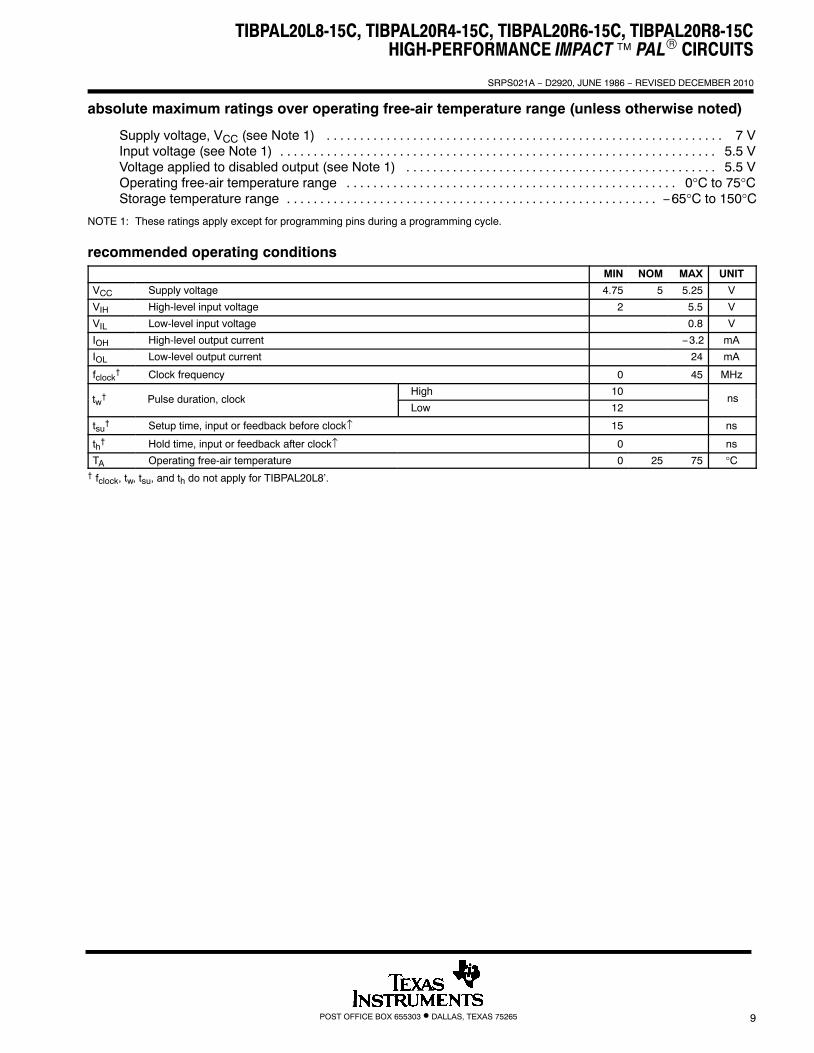
absolute maximum ratings over operating free-air temperature range (unless otherwise noted)
Supply voltage, VCC (see Note 1) 7 V. . . . . . . . . . . . . . . . . . . . . . . . . . . . . . . . . . . . . . . . . . . . . . . . . . . . . . . . . . . . Input voltage (see Note 1) 5.5 V. . . . . . . . . . . . . . . . . . . . . . . . . . . . . . . . . . . . . . . . . . . . . . . . . . . . . . . . . . . . . . . . . . Voltage applied to disabled output (see Note 1) 5.5 V. . . . . . . . . . . . . . . . . . . . . . . . . . . . . . . . . . . . . . . . . . . . . . . Operating free-air temperature range 0°C to 75°C. . . . . . . . . . . . . . . . . . . . . . . . . . . . . . . . . . . . . . . . . . . . . . . . . . Storage temperature range −65°C to 150°C. . . . . . . . . . . . . . . . . . . . . . . . . . . . . . . . . . . . . . . . . . . . . . . . . . . . . . . .
NOTE 1: These ratings apply except for programming pins during a programming cycle.
recommended operating conditionsMIN NOM MAX UNIT
VCC Supply voltage 4.75 5 5.25 V
VIH High-level input voltage 2 5.5 V
VIL Low-level input voltage 0.8 V
IOH High-level output current −3.2 mA
IOL Low-level output current 24 mA
fclock† Clock frequency 0 45 MHz
High 10
Low 12
tsu† Setup time, input or feedback before clock↑ 15 ns
th† Hold time, input or feedback after clock↑ 0 ns
TA Operating free-air temperature 0 25 75 °C† fclock, tw, tsu, and th do not apply for TIBPAL20L8’.
nsPulse duration, clock tw†
VO = 0.4 VIOZL VCC = 5.25 V, μA
VO = 2.7 VIOZH VCC = 5.25 V, μA
fmax¶ MHz
TIBPAL20L8-15C, TIBPAL20R4-15C, TIBPAL20R6-15C, TIBPAL20R8-15CHIGH-PERFORMANCE IMPACT�™ PAL® CIRCUITS
SRPS021A − D2920, JUNE 1986 − REVISED DECEMBER 2010
POST OFFICE BOX 655303 • DALLAS, TEXAS 7526510
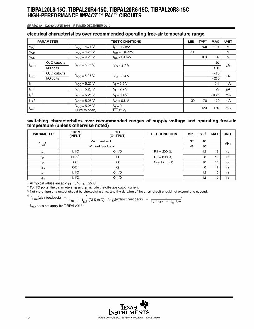
electrical characteristics over recommended operating free-air temperature range
PARAMETER TEST CONDITIONS MIN TYP† MAX UNIT
VIK VCC = 4.75 V, II = −18 mA −0.8 −1.5 V
VOH VCC = 4.75 V, IOH = −3.2 mA 2.4 V
VOL VCC = 4.75 V, IOL = 24 mA 0.3 0.5 V
O, Q outputs 20
I/O ports 100
O, Q outputs −20
I/O ports −250
II VCC = 5.25 V, VI = 5.5 V 0.1 mA
IIH‡ VCC = 5.25 V, VI = 2.7 V 25 μA
IIL‡ VCC = 5.25 V, VI = 0.4 V −0.25 mA
IOS§ VCC = 5.25 V, VO = 0.5 V −30 −70 −130 mA
ICCVCC = 5.25 V,Outputs open,
VI = 0,OE at VIH
120 180 mA
switching characteristics over recommended ranges of supply voltage and operating free-airtemperature (unless otherwise noted)
PARAMETERFROM
(INPUT)TO
(OUTPUT) TEST CONDITION MIN TYP† MAX UNIT
With feedback 37 40
Without feedback 45 50
tpd I, I/O O, I/O R1 = 200 Ω, 12 15 ns
tpd CLK↑ Q R2 = 390 Ω, 8 12 ns
ten OE Q See Figure 3 10 15 ns
tdis OE↑ Q 8 12 ns
ten I, I/O O, I/O 12 18 ns
tdis I, I/O O, I/O 12 15 ns† All typical values are at VCC = 5 V, TA = 25°C.‡ For I/O ports, the parameters IIH and IIL include the off-state output current.§ Not more than one output should be shorted at a time, and the duration of the short-circuit should not exceed one second.¶
fmax(with feedback) �1
tsu � tpd (CLK to Q),
fmax(without feedback) �1
tw high � tw low
,
fmax does not apply for TIBPAL20L8,.
TIBPAL20L8-20M, TIBPAL20R4-20M, TIBPAL20R6-20M, TIBPAL20R8-20MHIGH-PERFORMANCE IMPACT�™ PAL® CIRCUITS
SRPS021A − D2920, JUNE 1986 − REVISED DECEMBER 2010
POST OFFICE BOX 655303 • DALLAS, TEXAS 75265 11
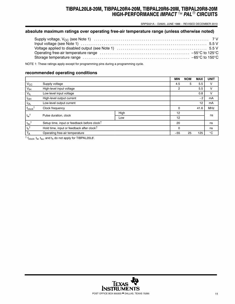
absolute maximum ratings over operating free-air temperature range (unless otherwise noted)
Supply voltage, VCC (see Note 1) 7 V. . . . . . . . . . . . . . . . . . . . . . . . . . . . . . . . . . . . . . . . . . . . . . . . . . . . . . . . . . . . Input voltage (see Note 1) 5.5 V. . . . . . . . . . . . . . . . . . . . . . . . . . . . . . . . . . . . . . . . . . . . . . . . . . . . . . . . . . . . . . . . . . Voltage applied to disabled output (see Note 1) 5.5 V. . . . . . . . . . . . . . . . . . . . . . . . . . . . . . . . . . . . . . . . . . . . . . . Operating free-air temperature range −55°C to 125°C. . . . . . . . . . . . . . . . . . . . . . . . . . . . . . . . . . . . . . . . . . . . . . . Storage temperature range −65°C to 150°C. . . . . . . . . . . . . . . . . . . . . . . . . . . . . . . . . . . . . . . . . . . . . . . . . . . . . . . .
NOTE 1: These ratings apply except for programming pins during a programming cycle.
recommended operating conditionsMIN NOM MAX UNIT
VCC Supply voltage 4.5 5 5.5 V
VIH High-level input voltage 2 5.5 V
VIL Low-level input voltage 0.8 V
IOH High-level output current −2 mA
IOL Low-level output current 12 mA
fclock† Clock frequency 0 41.6 MHz
High 12
Low 12
tsu† Setup time, input or feedback before clock↑ 20 ns
th† Hold time, input or feedback after clock↑ 0 ns
TA Operating free-air temperature −55 25 125 °C† fclock, tw, tsu, and th do not apply for TIBPAL20L8’.
nsPulse duration, clock tw†
μAVI = 2.7 V
VO = 0.4 V
VCC = 5.5 V,IIH‡
IOZL‡ VCC = 5.5 V, μA
fmax¶ MHz
TIBPAL20L8-20M, TIBPAL20R4-20M, TIBPAL20R6-20M, TIBPAL20R8-20MHIGH-PERFORMANCE IMPACT�™ PAL® CIRCUITS
SRPS021A − D2920, JUNE 1986 − REVISED DECEMBER 2010
POST OFFICE BOX 655303 • DALLAS, TEXAS 7526512
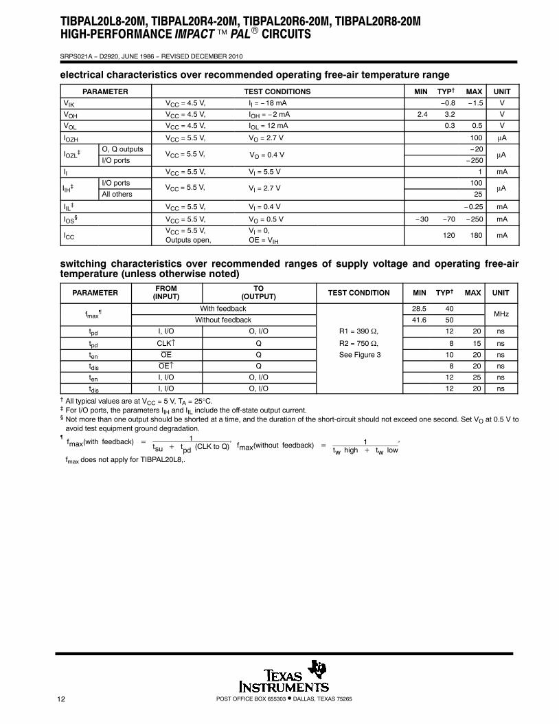
electrical characteristics over recommended operating free-air temperature range
PARAMETER TEST CONDITIONS MIN TYP† MAX UNIT
VIK VCC = 4.5 V, II = −18 mA −0.8 −1.5 V
VOH VCC = 4.5 V, IOH = −2 mA 2.4 3.2 V
VOL VCC = 4.5 V, IOL = 12 mA 0.3 0.5 V
IOZH VCC = 5.5 V, VO = 2.7 V 100 μA
O, Q outputs −20
I/O ports −250
II VCC = 5.5 V, VI = 5.5 V 1 mA
I/O ports 100
All others 25
IIL‡ VCC = 5.5 V, VI = 0.4 V −0.25 mA
IOS§ VCC = 5.5 V, VO = 0.5 V −30 −70 −250 mA
ICCVCC = 5.5 V,Outputs open,
VI = 0,OE = VIH
120 180 mA
switching characteristics over recommended ranges of supply voltage and operating free-airtemperature (unless otherwise noted)
PARAMETERFROM
(INPUT)TO
(OUTPUT) TEST CONDITION MIN TYP† MAX UNIT
With feedback 28.5 40
Without feedback 41.6 50
tpd I, I/O O, I/O R1 = 390 Ω, 12 20 ns
tpd CLK↑ Q R2 = 750 Ω, 8 15 ns
ten OE Q See Figure 3 10 20 ns
tdis OE↑ Q 8 20 ns
ten I, I/O O, I/O 12 25 ns
tdis I, I/O O, I/O 12 20 ns† All typical values are at VCC = 5 V, TA = 25°C.‡ For I/O ports, the parameters IIH and IIL include the off-state output current.§ Not more than one output should be shorted at a time, and the duration of the short-circuit should not exceed one second. Set VO at 0.5 V to
avoid test equipment ground degradation.¶
fmax(with feedback) �1
tsu � tpd (CLK to Q),
fmax(without feedback) �1
tw high � tw low
,
fmax does not apply for TIBPAL20L8,.
TIBPAL20L8-15C, TIBPAL20R4-15C, TIBPAL20R6-15C, TIBPAL20R8-15CTIBPAL20L8-20M, TIBPAL20R4-20M, TIBPAL20R6-20M, TIBPAL20R8-20M
HIGH-PERFORMANCE IMPACT�™ PAL® CIRCUITSSRPS021A − D2920, JUNE 1986 − REVISED DECEMBER 2010
POST OFFICE BOX 655303 • DALLAS, TEXAS 75265 13
programming information
Texas Instruments programmable logic devices can be programmed using widely available software andinexpensive device programmers.
Complete programming specifications, algorithms, and the latest information on hardware, software, andfirmware are available upon request. Information on programmers capable of programming Texas Instrumentsprogrammable logic is also available, upon request, from the nearest TI field sales office, local authorized TIdistributor, or by calling Texas Instruments at (214) 997-5666.
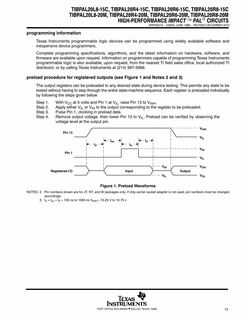
preload procedure for registered outputs (see Figure 1 and Notes 2 and 3)
The output registers can be preloaded to any desired state during device testing. This permits any state to betested without having to step through the entire state-machine sequence. Each register is preloaded individuallyby following the steps given below.
Step 1. With VCC at 5 volts and Pin 1 at VIL, raise Pin 13 to VIHH.Step 2. Apply either VIL or VIH to the output corresponding to the register to be preloaded.Step 3. Pulse Pin 1, clocking in preload data.Step 4. Remove output voltage, then lower Pin 13 to VIL. Preload can be verified by observing the
voltage level at the output pin.
tdtsu
twtd
VIHH
VIL
VIL
VOL
VOH
VIH
Pin 13
Pin 1
Registered I/O Input OutputVIH
VIL
Figure 1. Preload WaveformsNOTES: 2. Pin numbers shown are for JT, NT, and W packages only. If chip carrier socket adapter is not used, pin numbers must be changed
accordingly.3. td = tsu = th = 100 ns to 1000 ns VIHH = 10.25 V to 10.75 v
TIBPAL20L8-15C, TIBPAL20R4-15C, TIBPAL20R6-15C, TIBPAL20R8-15CTIBPAL20L8-20M, TIBPAL20R4-20M, TIBPAL20R6-20M, TIBPAL20R8-20MHIGH-PERFORMANCE IMPACT�™ PAL® CIRCUITSSRPS021 D− D2920, JUNE 1986 − REVISED DECEMBER 2010
POST OFFICE BOX 655303 • DALLAS, TEXAS 7526514
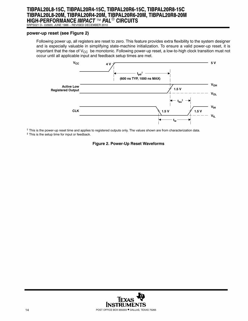
power-up reset (see Figure 2)
Following power up, all registers are reset to zero. This feature provides extra flexibility to the system designerand is especially valuable in simplifying state-machine initialization. To ensure a valid power-up reset, it isimportant that the rise of VCC be monotonic. Following power-up reset, a low-to-high clock transition must notoccur until all applicable input and feedback setup times are met.
1.5 V
tsu‡
tpd†
tw
VIL
VIH
5 VVCC
Active LowRegistered Output
CLK
4 V
VOH
VOL
1.5 V
(600 ns TYP, 1000 ns MAX)
1.5 V
† This is the power-up reset time and applies to registered outputs only. The values shown are from characterization data.‡ This is the setup time for input or feedback.
Figure 2. Power-Up Reset Waveforms
TIBPAL20L8-15C, TIBPAL20R4-15C, TIBPAL20R6-15C, TIBPAL20R8-15CTIBPAL20L8-20M, TIBPAL20R4-20M, TIBPAL20R6-20M, TIBPAL20R8-20M
HIGH-PERFORMANCE IMPACT�™ PAL® CIRCUITSSRPS021A − D2920, JUNE 1986 − REVISED DECEMBER 2010
POST OFFICE BOX 655303 • DALLAS, TEXAS 75265 15
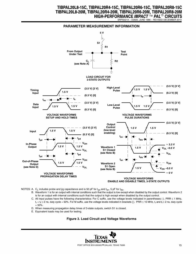
PARAMETER MEASUREMENT INFORMATION
tsu
S1
R2CL(see Note A)
LOAD CIRCUIT FOR3-STATE OUTPUTS
(3.5 V) [3 V]
(0.3 V) [0]
1.5 V
1.5 V
th
1.5 V
tpd
tpd
tpd
tpd
VOLTAGE WAVEFORMSSETUP AND HOLD TIMES
VOLTAGE WAVEFORMSPROPAGATION DELAY TIMES
VOH
VOH
VOL
VOL
1.5 V 1.5 V
1.5 V 1.5 V
tw
1.5 V 1.5 V
≈ 3.3 V
VOL
VOH
VOH −0.5 V
≈ 0 V
ten
ten
tdis
tdis
VOLTAGE WAVEFORMSENABLE AND DISABLE TIMES, 3-STATE OUTPUTS
VOLTAGE WAVEFORMSPULSE DURATIONS
1.5 V 1.5 V
1.5 V
1.5 V 1.5 V
1.5 V 1.5 V
1.5 V
R1
VOL +0.5 V
5 V
(3.5 V) [3 V]
(0.3 V) [0]
(3.5 V) [3 V]
(0.3 V) [0]
(3.5 V) [3 V]
(0.3 V) [0]
(3.5 V) [3 V]
(0.3 V) [0]
(3.5 V) [3 V]
(0.3 V) [0]
From Output Under Test
TestPoint
Input
Out-of-PhaseOutput
(see Note D)
TimingInput
DataInput
In-PhaseOutput
High-LevelPulse
Low-LevelPulse
OutputControl
(low-levelenabling)
Waveform 1S1 Closed
(see Note B)
Waveform 2S1 Open
(see Note B)
NOTES: A. CL includes probe and jig capacitance and is 50 pF for tpd and ten, 5 pF for tdis.B. Waveform 1 is for an output with internal conditions such that the output is low except when disabled by the output control. Waveform 2
is for an output with internal conditions such that the output is high except when disabled by the output control.C. All input pulses have the following characteristics: For C suffix, use the voltage levels indicated in parentheses ( ). PRR ≤ 1 MHz,
tr = tf ≤ 2 ns, duty cycle = 50%. For M suffix, use the voltage levels indicated in brackets [ ]. PRR ≤ 10 MHz, tr and tf ≤ 2 ns, duty cycle= 50%.
D. When measuring propagation delay times of 3-state outputs, switch S1 is closed.E. Equivalent loads may be used for testing.
Figure 3. Load Circuit and Voltage Waveforms
D0892
North AmericanTI Authorized
Distributors
CustomerResponse CenterTOLL FREE: (800) 336-5236OUTSIDE USA: (214) 995-6611
(8:00 a.m. − 5:00 p.m. CST)
TI Die ProcessorsChip Supply (407) 298-7100Elmo Semiconductor (818) 768-7400Minco Technology Labs (512) 834-2022
©1992 Texas Instruments Incorporated
SRPS021
TI NorthAmerican SalesOfficesALABAMA: Huntsville: (205) 837-7530ARIZONA: Phoenix: (602) 995-1007CALIFORNIA: Irvine: (714) 660-1200San Diego: (619) 278-9600Santa Clara: (408) 980-9000Woodland Hills: (818) 704-8100COLORADO: Aurora: (303) 368-8000CONNECTICUT: Wallingford: (203) 269-0074FLORIDA: Altamonte Springs: (407) 260-2116Fort Lauderdale: (305) 973-8502Tampa: (813) 885-7588GEORGIA: Norcross: (404) 662-7967ILLINOIS: Arlington Heights: (708) 640-3000INDIANA: Carmel: (317) 573-6400Fort Wayne: (219) 489-4697KANSAS: Overland Park: (913) 451-4511MARYLAND: Columbia: (410) 964-2003MASSACHUSETTS: Waltham: (617) 895-9100MICHIGAN: Farmington Hills: (313) 553-1581MINNESOTA: Eden Prairie: (612) 828-9300MISSOURI: St. Louis: (314) 821-8400NEW JERSEY: Iselin: (908) 750-1050NEW MEXICO: Albuquerque: (505) 345-2555NEW YORK: East Syracuse: (315) 463-9291Fishkill: (914) 897-2900Melville: (516) 454-6600Pittsford: (716) 385-6770NORTH CAROLINA: Charlotte: (704) 527-0930Raleigh: (919) 876-2725OHIO: Beachwood: (216) 765-7258Beavercreek: (513) 427-6200OREGON: Beaverton: (503) 643-6758PENNSYLVANIA: Blue Bell: (215) 825-9500PUERTO RICO: Hato Rey: (809) 753-8700TEXAS: Austin: (512) 250-6769Dallas: (214) 917-1264Houston: (713) 778-6592Midland: (915) 561-7137UTAH: Salt Lake CIty: (801) 466-8972WISCONSIN: Waukesha: (414) 798-1001CANADA: Nepean: (613) 726-1970Richmond Hill: (416) 884-9181St. Laurent: (514) 335-8392
TI RegionalTechnologyCentersCALIFORNIA: Irvine: (714) 660-8140 Santa Clara: (408) 748-2222GEORGIA: Norcross: (404) 662-7945ILLINOIS: Arlington Heights: (708) 640-2909INDIANA: Indianapolis: (317) 573-6400MASSACHUSETTS: Waltham: (617) 895-9196MEXICO: Mexico City: 491-70834MINNESOTA: Minneapolis: (612) 828-9300TEXAS: Dallas: (214) 917-3881CANADA: Nepean: (613) 726-1970
Alliance Electronics, Inc. (military product only)Almac/ArrowAnthem Electronics Arrow/SchweberFuture Electronics (Canada) GRS Electronics Co., Inc. Hall-Mark Electronics Marshall Industries Newark Electronics Rochester Electronics, Inc. (obsolete product only (508) 462-9332) Wyle Laboratories Zeus Components
TI DistributorsALABAMA: Arrow/Schweber (205) 837-6955; Hall-Mark(205) 837-8700; Marshall (205) 881-9235.ARIZONA: Anthem (602) 966-6600; Arrow/Schweber (602)437-0750; Hall-Mark (602) 431-0030; Marshall (602)496-0290; Wyle (602) 437-2088.CALIFORNIA: Los Angeles/Orange County: Anthem(818) 775-1333, (714) 768-4444; Arrow/Schweber (818)380-9686, (714) 838-5422; Hall-Mark (818) 773-4500, (714)727-6000; Marshall (818) 878-7000, (714) 458-5301; Wyle(818) 880-9000, (714) 863-9953; Zeus (714) 921-9000,(818) 889-3838;Sacramento: Anthem (916) 624-9744; Hall-Mark (916)624-9781; Marshall (916) 635-9700; Wyle (916) 638-5282;San Diego: Anthem (619) 453-9005; Arrow/Schweber(619) 565-4800; Hall-Mark (619) 268-1201; Marshall (619)578-9600; Wyle (619) 565-9171; Zeus (619) 277-9681.San Francisco Bay Area: Anthem (408) 453-1200;Arrow/Schweber (408) 441-9700, (510) 490-9477;Hall-Mark (408) 432-4000; Marshall (408) 942-4600;Wyle (408) 727-2500; Zeus (408) 629-4789.COLORADO: Anthem (303) 790-4500; Arrow/Schweber(303) 799-0258; Hall-Mark (303) 790-1662; Marshall (303)451-8383; Wyle (303) 457-9953.CONNECTICUT: Anthem (203) 575-1575; Arrow/Schweber(203) 265-7741; Hall-Mark (203) 271-2844; Marshall (203)265-3822.FLORIDA: Fort Lauderdale: Arrow/Schweber (305)429-8200; Halll-Mark (305) 971-9280; Marshall (305)977-4880.Orlando: Arrow/Schweber (407) 333-9300; Hall-Mark (407)830-5855; Marshall (407) 767-8585; Zeus (407) 788-9100.Tampa: Hall-Mark (813) 541-7440; Marshall (813)573-1399.GEORGIA: Arrow/Schweber (404) 497-1300; Hall-Mark(404) 623-4400; Marshall (404) 923-5750.ILLINOIS: Anthem (708) 884-0200; Arrow/Schweber (708)250-0500; Hall-Mark (312) 860-3800; Marshall (708)490-0155; Newark (312)784-5100.INDIANA: Arrow/Schweber (317) 299-2071; Hall-Mark(317) 872-8875; Marshall (317) 297-0483.IOWA: Arrow/Schweber (319) 395-7230.KANSAS: Arrow/Schweber (913) 541-9542; Hall-Mark(913) 888-4747; Marshall (913) 492-3121.MARYLAND: Anthem (301) 995-6640; Arrow/Schweber(301) 596-7800; Hall-Mark (301) 988-9800; Marshall (301)622-1118; Zeus (301) 997-1118.MASSACHUSETTS: Anthem (508) 657-5170;Arrow/Schweber (508) 658-0900; Hall-Mark (508)667-0902; Marshall (508) 658-0810; Wyle (617) 272-7300;Zeus (617) 246-8200.
MICHIGAN: Detroit: Arrow/Schweber (313) 462-2290;Hall-Mark (313) 416-5800; Marshall (313) 525-5850;Newark (313) 967-0600.MINNESOTA: Anthem (612) 944-5454; Arrow/Schweber(612) 941-5280; Hall-Mark (612) 881-2600; Marshall (612)559-2211.MISSOURI: Arrow/Schweber (314) 567-6888; Hall-Mark(314) 291-5350; Marshall (314) 291-4650.NEW JERSEY: Anthem (201) 227-7960; Arrow/Schweber(201) 227-7880, (609) 596-8000; Hall-Mark (201) 515-3000,(609) 235-1900; Marshall (201) 882-0320, (609) 234-9100.NEW MEXICO: Alliance (505) 292-3360.NEW YORK: Long Island: Anthem (516) 864-6600;Arrow/Schweber (516) 231-1000; Hall-Mark (516)737-0600; Marshall (516) 273-2424; Zeus (914) 937-7400.Rochester: Arrow/Schweber (716) 427-0300; Hall-Mark(716) 425-3300; Marshall (716) 235-7620.Syracuse: Marshall (607) 785-2345.NORTH CAROLINA: Arrow/Schweber (919) 876-3132;Hall-Mark (919) 872-0712; Marshall (919) 878-9882.OHIO: Cleveland: Arrow/Schweber (216) 248-3990;Hall-Mark (216) 349-4632; Marshall (216) 248-1788.Columbus: Hall-Mark (614) 888-3313.Dayton: Arrow/Schweber (513) 435-5563; Marshall (513)898-4480; Zeus (513) 293-6162.OKLAHOMA: Arrow/Schweber (918) 252-7537; Hall-Mark(918) 254-6110.OREGON: Almac/Arrow (503) 629-8090; Anthem (503)643-1114; Marshall (503) 644-5050; Wyle (503) 643-7900.PENNSYLVANIA: Anthem (215) 443-5150;Arrow/Schweber (215) 928-1800; GRS (215) 922-7037;(609) 964-8560; Marshall (412) 788-0441.TEXAS: Austin: Arrow/Schweber (512) 835-4180;Hall-Mark (512) 258-8848; Marshall (512) 837-1991; Wyle(512) 345-8853;Dallas: Anthem (214) 238-7100; Arrow/Schweber (214)380-6464; Hall-Mark (214) 553-4300; Marshall (214)233-5200; Wyle (214) 235-9953; Zeus (214) 783-7010;Houston: Arrow/Schweber (713) 530-4700; Hall-Mark (713) 781-6100; Marshall (713) 467-1666; Wyle (713)879-9953.UTAH: Anthem (801) 973-8555; Arrow/Schweber (801)973-6913; Marshall (801) 973-2288; Wyle (801) 974-9953.WASHINGTON: Almac/Arrow (206) 643-9992, Anthem(206) 483-1700; Marshall (206) 486-5747; Wyle (206)881-1150.WISCONSIN: Arrow/Schweber (414) 792-0150; Hall-Mark(414) 797-7844; Marshall (414) 797-8400.CANADA: Calgary: Future (403) 235-5325;Edmonton: Future (403) 438-2858;Montreal: Arrow/Schweber (514) 421-7411; Future (514)694-7710; Marshall (514) 694-8142Ottawa: Arrow/Schweber (613) 226-6903; Future (613)820-8313.Quebec: Future (418) 897-6666.Toronto: Arrow/Schweber (416) 670-7769; Future (416) 612-9200; Marshall (416) 458-8046.Vancouver: Arrow/Schweber (604) 421-2333; Future (604) 294-1166.
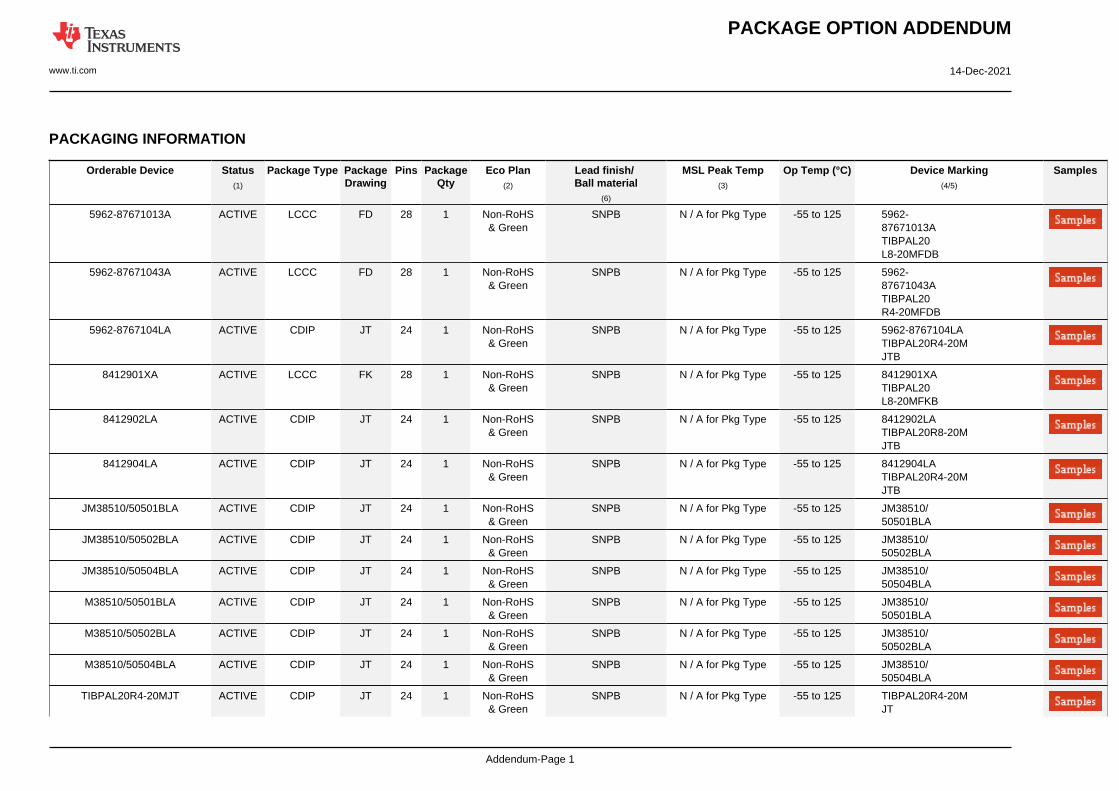
PACKAGE OPTION ADDENDUM
www.ti.com 14-Dec-2021
Addendum-Page 1
PACKAGING INFORMATION
Orderable Device Status(1)
Package Type PackageDrawing
Pins PackageQty
Eco Plan(2)
Lead finish/Ball material
(6)
MSL Peak Temp(3)
Op Temp (°C) Device Marking(4/5)
Samples
5962-87671013A ACTIVE LCCC FD 28 1 Non-RoHS& Green
SNPB N / A for Pkg Type -55 to 125 5962-87671013ATIBPAL20L8-20MFDB
5962-87671043A ACTIVE LCCC FD 28 1 Non-RoHS& Green
SNPB N / A for Pkg Type -55 to 125 5962-87671043ATIBPAL20R4-20MFDB
5962-8767104LA ACTIVE CDIP JT 24 1 Non-RoHS& Green
SNPB N / A for Pkg Type -55 to 125 5962-8767104LATIBPAL20R4-20MJTB
8412901XA ACTIVE LCCC FK 28 1 Non-RoHS& Green
SNPB N / A for Pkg Type -55 to 125 8412901XATIBPAL20L8-20MFKB
8412902LA ACTIVE CDIP JT 24 1 Non-RoHS& Green
SNPB N / A for Pkg Type -55 to 125 8412902LATIBPAL20R8-20MJTB
8412904LA ACTIVE CDIP JT 24 1 Non-RoHS& Green
SNPB N / A for Pkg Type -55 to 125 8412904LATIBPAL20R4-20MJTB
JM38510/50501BLA ACTIVE CDIP JT 24 1 Non-RoHS& Green
SNPB N / A for Pkg Type -55 to 125 JM38510/50501BLA
JM38510/50502BLA ACTIVE CDIP JT 24 1 Non-RoHS& Green
SNPB N / A for Pkg Type -55 to 125 JM38510/50502BLA
JM38510/50504BLA ACTIVE CDIP JT 24 1 Non-RoHS& Green
SNPB N / A for Pkg Type -55 to 125 JM38510/50504BLA
M38510/50501BLA ACTIVE CDIP JT 24 1 Non-RoHS& Green
SNPB N / A for Pkg Type -55 to 125 JM38510/50501BLA
M38510/50502BLA ACTIVE CDIP JT 24 1 Non-RoHS& Green
SNPB N / A for Pkg Type -55 to 125 JM38510/50502BLA
M38510/50504BLA ACTIVE CDIP JT 24 1 Non-RoHS& Green
SNPB N / A for Pkg Type -55 to 125 JM38510/50504BLA
TIBPAL20R4-20MJT ACTIVE CDIP JT 24 1 Non-RoHS& Green
SNPB N / A for Pkg Type -55 to 125 TIBPAL20R4-20MJT
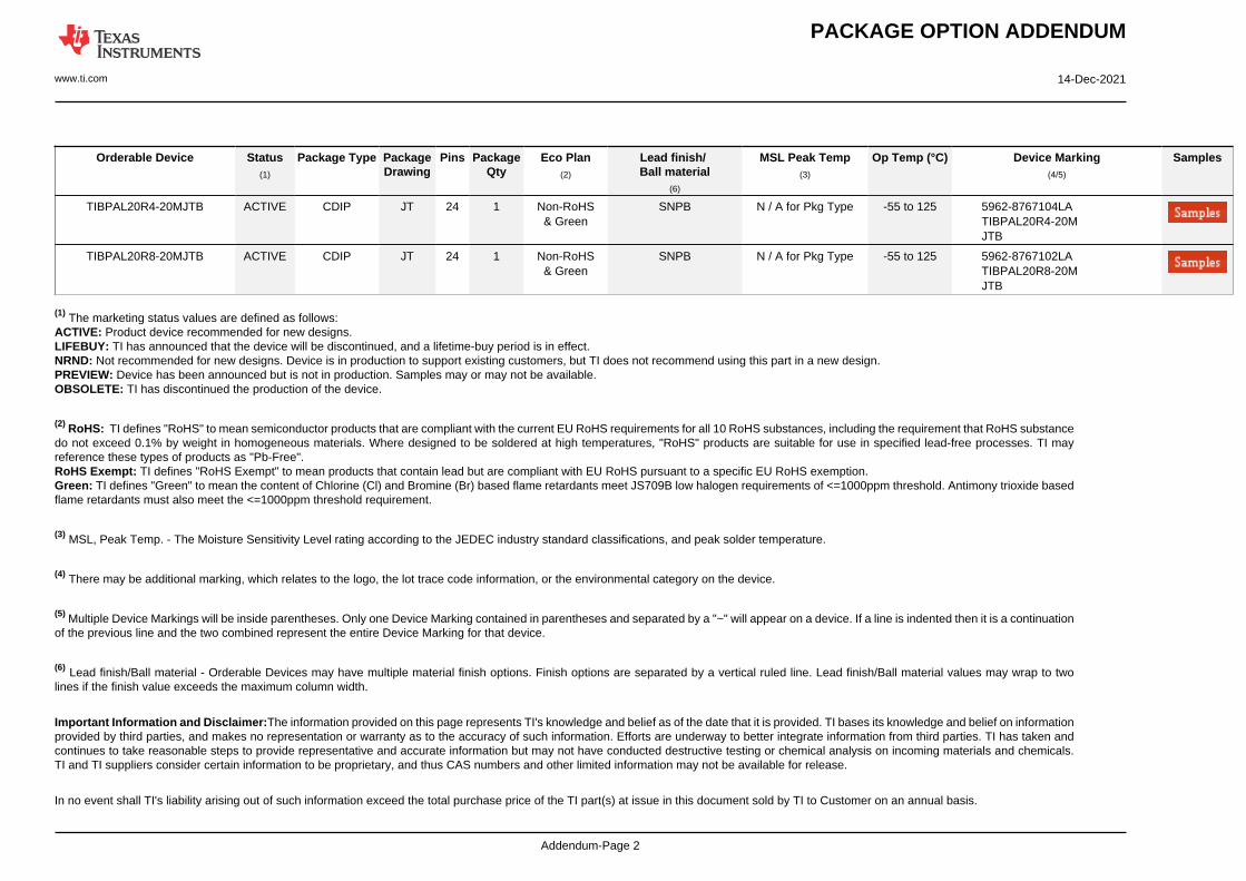
PACKAGE OPTION ADDENDUM
www.ti.com 14-Dec-2021
Addendum-Page 2
Orderable Device Status(1)
Package Type PackageDrawing
Pins PackageQty
Eco Plan(2)
Lead finish/Ball material
(6)
MSL Peak Temp(3)
Op Temp (°C) Device Marking(4/5)
Samples
TIBPAL20R4-20MJTB ACTIVE CDIP JT 24 1 Non-RoHS& Green
SNPB N / A for Pkg Type -55 to 125 5962-8767104LATIBPAL20R4-20MJTB
TIBPAL20R8-20MJTB ACTIVE CDIP JT 24 1 Non-RoHS& Green
SNPB N / A for Pkg Type -55 to 125 5962-8767102LATIBPAL20R8-20MJTB
(1) The marketing status values are defined as follows:ACTIVE: Product device recommended for new designs.LIFEBUY: TI has announced that the device will be discontinued, and a lifetime-buy period is in effect.NRND: Not recommended for new designs. Device is in production to support existing customers, but TI does not recommend using this part in a new design.PREVIEW: Device has been announced but is not in production. Samples may or may not be available.OBSOLETE: TI has discontinued the production of the device.
(2) RoHS: TI defines "RoHS" to mean semiconductor products that are compliant with the current EU RoHS requirements for all 10 RoHS substances, including the requirement that RoHS substancedo not exceed 0.1% by weight in homogeneous materials. Where designed to be soldered at high temperatures, "RoHS" products are suitable for use in specified lead-free processes. TI mayreference these types of products as "Pb-Free".RoHS Exempt: TI defines "RoHS Exempt" to mean products that contain lead but are compliant with EU RoHS pursuant to a specific EU RoHS exemption.Green: TI defines "Green" to mean the content of Chlorine (Cl) and Bromine (Br) based flame retardants meet JS709B low halogen requirements of <=1000ppm threshold. Antimony trioxide basedflame retardants must also meet the <=1000ppm threshold requirement.
(3) MSL, Peak Temp. - The Moisture Sensitivity Level rating according to the JEDEC industry standard classifications, and peak solder temperature.
(4) There may be additional marking, which relates to the logo, the lot trace code information, or the environmental category on the device.
(5) Multiple Device Markings will be inside parentheses. Only one Device Marking contained in parentheses and separated by a "~" will appear on a device. If a line is indented then it is a continuationof the previous line and the two combined represent the entire Device Marking for that device.
(6) Lead finish/Ball material - Orderable Devices may have multiple material finish options. Finish options are separated by a vertical ruled line. Lead finish/Ball material values may wrap to twolines if the finish value exceeds the maximum column width.
Important Information and Disclaimer:The information provided on this page represents TI's knowledge and belief as of the date that it is provided. TI bases its knowledge and belief on informationprovided by third parties, and makes no representation or warranty as to the accuracy of such information. Efforts are underway to better integrate information from third parties. TI has taken andcontinues to take reasonable steps to provide representative and accurate information but may not have conducted destructive testing or chemical analysis on incoming materials and chemicals.TI and TI suppliers consider certain information to be proprietary, and thus CAS numbers and other limited information may not be available for release.
In no event shall TI's liability arising out of such information exceed the total purchase price of the TI part(s) at issue in this document sold by TI to Customer on an annual basis.
PACKAGE OPTION ADDENDUM
www.ti.com 14-Dec-2021
Addendum-Page 3
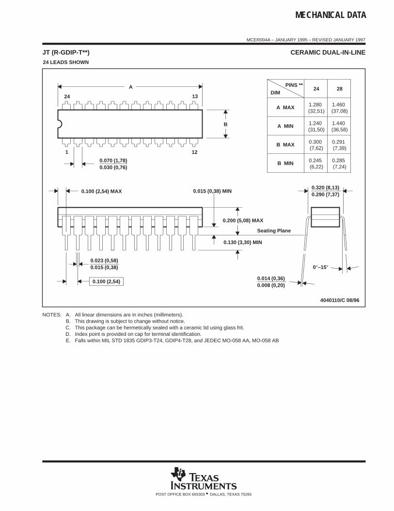
MECHANICAL DATA
MCER004A – JANUARY 1995 – REVISED JANUARY 1997
POST OFFICE BOX 655303 • DALLAS, TEXAS 75265
JT (R-GDIP-T**) CERAMIC DUAL-IN-LINE24 LEADS SHOWN
4040110/C 08/96
B
0.200 (5,08) MAX
0.320 (8,13)0.290 (7,37)
0.130 (3,30) MIN
0.008 (0,20)0.014 (0,36)
Seating Plane
13
12
0.030 (0,76)0.070 (1,78)
0.015 (0,38) MIN
A
24
1
0.100 (2,54) MAX
0.023 (0,58)0.015 (0,38)
0.100 (2,54)
0°–15°
1.440
(37,08) 1.460
0.285
(7,39) 0.291
(36,58)
(7,24)
28PINS **
1.280
1.240
0.300
0.245
(7,62)
DIM
B MAX
A MAX
A MIN
B MIN(6,22)
24
(32,51)
(31,50)
NOTES: A. All linear dimensions are in inches (millimeters).B. This drawing is subject to change without notice.C. This package can be hermetically sealed with a ceramic lid using glass frit.D. Index point is provided on cap for terminal identification.E. Falls within MIL STD 1835 GDIP3-T24, GDIP4-T28, and JEDEC MO-058 AA, MO-058 AB

IMPORTANT NOTICE AND DISCLAIMERTI PROVIDES TECHNICAL AND RELIABILITY DATA (INCLUDING DATA SHEETS), DESIGN RESOURCES (INCLUDING REFERENCE DESIGNS), APPLICATION OR OTHER DESIGN ADVICE, WEB TOOLS, SAFETY INFORMATION, AND OTHER RESOURCES “AS IS” AND WITH ALL FAULTS, AND DISCLAIMS ALL WARRANTIES, EXPRESS AND IMPLIED, INCLUDING WITHOUT LIMITATION ANY IMPLIED WARRANTIES OF MERCHANTABILITY, FITNESS FOR A PARTICULAR PURPOSE OR NON-INFRINGEMENT OF THIRD PARTY INTELLECTUAL PROPERTY RIGHTS.These resources are intended for skilled developers designing with TI products. You are solely responsible for (1) selecting the appropriate TI products for your application, (2) designing, validating and testing your application, and (3) ensuring your application meets applicable standards, and any other safety, security, regulatory or other requirements.These resources are subject to change without notice. TI grants you permission to use these resources only for development of an application that uses the TI products described in the resource. Other reproduction and display of these resources is prohibited. No license is granted to any other TI intellectual property right or to any third party intellectual property right. TI disclaims responsibility for, and you will fully indemnify TI and its representatives against, any claims, damages, costs, losses, and liabilities arising out of your use of these resources.TI’s products are provided subject to TI’s Terms of Sale or other applicable terms available either on ti.com or provided in conjunction with such TI products. TI’s provision of these resources does not expand or otherwise alter TI’s applicable warranties or warranty disclaimers for TI products.TI objects to and rejects any additional or different terms you may have proposed. IMPORTANT NOTICE
Mailing Address: Texas Instruments, Post Office Box 655303, Dallas, Texas 75265Copyright © 2021, Texas Instruments Incorporated