the measurement of thin film stress using phase shifting interferometry
TRANSCRIPT

This article was downloaded by: [Tufts University]On: 06 October 2014, At: 16:05Publisher: Taylor & FrancisInforma Ltd Registered in England and Wales Registered Number: 1072954Registered office: Mortimer House, 37-41 Mortimer Street, London W1T 3JH, UK
Journal of Modern OpticsPublication details, including instructions for authors andsubscription information:http://www.tandfonline.com/loi/tmop20
The measurement of thin film stressusing phase shifting interferometryChuen-Lin Tien a , Cheng-Chung Lee a & Cheng-Chung Jaing ba Institute of Optical Sciences, National Central University ,Chung-Li, 320, Taiwanb Research & Development Division , Precision InstrumentDevelopment Centre, National Science Council , Hsin-Chu,300, TaiwanPublished online: 03 Jul 2009.
To cite this article: Chuen-Lin Tien , Cheng-Chung Lee & Cheng-Chung Jaing (2000) Themeasurement of thin film stress using phase shifting interferometry, Journal of Modern Optics,47:5, 839-849
To link to this article: http://dx.doi.org/10.1080/09500340008235094
PLEASE SCROLL DOWN FOR ARTICLE
Taylor & Francis makes every effort to ensure the accuracy of all the information(the “Content”) contained in the publications on our platform. However, Taylor& Francis, our agents, and our licensors make no representations or warrantieswhatsoever as to the accuracy, completeness, or suitability for any purpose of theContent. Any opinions and views expressed in this publication are the opinions andviews of the authors, and are not the views of or endorsed by Taylor & Francis. Theaccuracy of the Content should not be relied upon and should be independentlyverified with primary sources of information. Taylor and Francis shall not be liablefor any losses, actions, claims, proceedings, demands, costs, expenses, damages,and other liabilities whatsoever or howsoever caused arising directly or indirectly inconnection with, in relation to or arising out of the use of the Content.
This article may be used for research, teaching, and private study purposes. Anysubstantial or systematic reproduction, redistribution, reselling, loan, sub-licensing,systematic supply, or distribution in any form to anyone is expressly forbidden.
Terms & Conditions of access and use can be found at http://www.tandfonline.com/page/terms-and-conditions
Dow
nloa
ded
by [
Tuf
ts U
nive
rsity
] at
16:
05 0
6 O
ctob
er 2
014

JOURNAL OF MODERN omcs, 2000, VOL. 47, NO. 5, 839-849
The measurement of thin film stress using phase shifting interferometry
CHUEN-LIN TIENt, CHENG-CHUNG LEE? and
t Institute of Optical Sciences, National Central University, Chung-Li, 320, Taiwan 1 Research & Development Division, Precision Instrument Development Centre, National Science Council, Hsin-Chu,
CHENG-CHUNG JAINGS
300, Taiwan
(Received 5 May 1999; revision received 20 September 999)
Abstract. A new technique for determining the stress of thin films is described. This technique combines digital phase shifting interferometry with image-processing software. A circular disc polished on one side is used as the coated substrate during film deposition. The average stress in thin films can be derived by comparing the deflection of the substrate before and after film deposition. The deflection of the substrate by the deposited film is obtained by the phase map. Using the Zernike polynomial fitting algorithm, a three- dimensional contour map is generated from the polynomial coefficients to visualize the deformation of the thin film and to examine the tensile or compressive stress after film deposition. Four oxide films prepared by ion- beam sputter deposition are investigated for their film stresses. The experi- mental results show that the stress values are concordant with measurements using other methods.
1. Introduction T h e stress behaviour of thin films is very important in all optical coating
applications. I t is well known that almost all thin films, produced by the various deposition techniques, have mechanical stresses. Stress in thin films is primarily composed of a thermal stress and an intrinsic stress [l]. T h e thermal stress is due to the difference in the thermal expansion coefficients between the coating and the substrate materials. T h e intrinsic stress is induced during the film-growth process, but the mechanisms are complex, and not yet fully understood. Film stress causes many undesirable phenomena, for example, the cracking or peeling of the film and the bending of the substrate. T o study thin film stress issues, it is necessary to understand the stress mechanisms and their effects. Therefore, the precise meas- urement of stress in thin films is of considerable importance in numerous industrial applications.
Many experimental techniques have been used to measure stress in thin films, including the interferometric technique [2-4], the cantilever beam (bending beam) technique [5-91, the X-ray diffraction technique [lo], the optically levered laser technique [l l-161 and the thermoelastic bending technique [17] etc. Most of these
Journal of Modern Optics ISSN 095C-0340 print/ISSN 1362-3044 online 0 2000 Taylor & Francis Ltd http://www.tandf.co.uk/journals/tf/O950034O.htrnl
Dow
nloa
ded
by [
Tuf
ts U
nive
rsity
] at
16:
05 0
6 O
ctob
er 2
014
840 C.-L. Tien et al.
techniques are based on the measurement of the curvature of a very thin substrate induced by the stress in the film, or based on the direct measurement of the bending force and the displacement, by traditional mechanical testing techniques. On the other hand, X-ray diffraction has been used to measure changes in the lattice spacing. The diffraction method is also suitable for measuring the strain- stress behaviour in thin films, but it is an indirect method, where the stress is calculated from the elastic strain. All the above methods are somewhat elaborate and need a special thin substrate or cantilever strip. In the traditional interfero- metry method, the stress of the thin film is measured by the interference fringes between a thin substrate and an optical flat, which are used to determine the deflection of the substrate. However it is difficult to find substrates with a thickness of -0.1 mm which are perfectly flat and the sensitivity is limited by the usable substrate thickness [3, 41. Therefore in this article, we shall develop a reliable and accurate phase shifting interferometry (PSI) technique, combined with image processing software, to measure the stress of thin films. The stress of optical coatings with ion beam sputter deposition is investigated. The measured stress of SiOz, TiOz, Taz05 and NbZOs films, deposited on a BK-7 substrate, is quite consistent with previous experiments using different techniques.
2. Method 2.1. Measurement technique
The optical arrangement for the PSI technique is based on a Twyman-Green interferometer, as shown in figure 1. A He-Ne laser passing through a micro- objective and a pinhole, acting as a spatial filter, form a point source and then propagate through a collimating lens to form a plane wavefront. The wavefront is divided in amplitude by a beam splitter. The reflected and transmitted beams travel to a reference plate and a test plate (a BK-7 substrate 25.4mm in diameter and 1.5 mm in thickness). The substrate is mounted on a sample holder and acts as a test plate. After being reflected by both the reference plate and the test plate, the beams recombine at the beam splitter and travel toward the detector (CCD). The interference pattern can be seen on a monitor through the CCD camera. We use a phase shifting Twyman-Green interferometer to measure the deformation of the fringes of a coated substrate. The phase shifting measurement principles follow Hariharan's algorithm [18] to detect the phase of the fringes. We set up a PC-based stress measurement system to determine the film stress. The phase shifting fringe patterns are obtained by moving the reference plate to five equally spaced positions of X/8, with a computer-controlled piezoelectric transducer (PZT) translation device. A programmable power supply controlled by a computer provides the PZT voltage.
For image acquisition and processing, the Hariharan algorithm requires that five separate interferograms of the part under test are recorded and digitized. A 90" phase shift is introduced into the reference beam between each sequential inter- ferogram recorded by a PC-based frame grabber board. In practise, there are five interferograms, with a constant phase difference (i.e. O", 90", 180", 270" and 360") between frames, used to generate the phase map of the fringe patterns. The phase of the fringe is calculated from the digitized intensities at each point in the interferograms using the following equation [ 181
Dow
nloa
ded
by [
Tuf
ts U
nive
rsity
] at
16:
05 0
6 O
ctob
er 2
014

The measurement of thin fi lm stress
Figure 1. Schematic of a phase shifting Twyman-Green interferometer.
841
where @ ( x , y ) is a phase function and I1 to 15 represent the digitized intensity at a particular point on the five interferograms. The above equation is evaluated at each measurement point to obtain a phase map of the measured wavefront. This wavefront is related to the surface height of the test plate or the optical path difference (OPD). For example, a surface with height errors of h ( x , y ) , tested by reflection, produces a wavefront phase @ ( x , y ) . The height errors or the OPD between the reference and the object wavefronts can be found from the phase by the following expression
where x and y are the spatial coordinates and A is the wavelength of the laser beam. If we define @, to be the wavefront phase at a distance r from the centre of a
circular substrate with radius p ( Y 5 p) , and @= is the wavefront phase at the centre of the substrate, then, assuming that the coating is thin with respect to the substrate thickness, the relative deflection of a circular substrate with parallel surfaces can be expressed as a function of the wavefront phase difference. We obtain
Dow
nloa
ded
by [
Tuf
ts U
nive
rsity
] at
16:
05 0
6 O
ctob
er 2
014

842 C.-L. Tien et al.
where Ah is the relative deflection at a distance Y from the centre of a circular substrate, and X is the wavelength of the He-Ne laser. Thin films deposited on a substrate will bend the substrate because of the stress. By measuring the difference in deflection between the substrate before and after thin film deposition, and assuming that the stress is isotropic, the stress in a thin film deposited on a substrate results in substrate deformation proportional to the film stress. Let 6 = (l/N)Ez, Ah,, where Ah, is the relative deflection at any position i at distance Y from the centre, and N is the number of sampling points. The film stress D can then be related to the deflection of the substrate at a distance Y from the centre of the substrate, by using the modified Stoney’s formulae [19, 201
E,d:6 D =
3y2(1 - v,)df’ (4)
where D is the stress in the thin film, 6 is the average deflection as defined above, and Y is the measured radius on the substrate. E, and v, are the Young’s modulus and the Poisson’s ratio of the substrate, respectively. d, is the thickness of the substrate and df (d f << d,) is the film thickness. The film thickness is determined by the envelope method of the optical transmission measurements. This treatment assumes an isotropic homogeneous stress distribution in the coating in which deformations of the substrate are small compared to the substrate thickness.
By convention, D is negative for compressive stress and positive for tensile stress. Tensile stress is present in the film if the curvature of the substrate is concave, conversely, the stress is compressive if the curvature of the substrate is convex. In other words, the deflection is downward for tensile stress and upward for compressive stress, as shown in figure 2. For this configuration, a sign of downward deflection is specified as positive.
Film Substrate
Film Substrate
Film Substrate
COMPRESSIVE S W S S
in the thin film. Figure 2. Deflection of a film-substrate combination due to compressive or tensile stress
Dow
nloa
ded
by [
Tuf
ts U
nive
rsity
] at
16:
05 0
6 O
ctob
er 2
014
The measurement of thin film stress 843
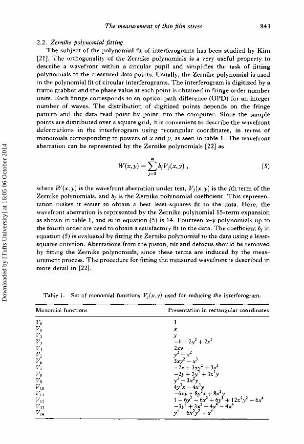
2 .2 . Zernike polynomial fitting The subject of the polynomial fit of interferograms has been studied by Kim
[21]. The orthogonality of the Zernike polynomials is a very useful property to describe a wavefront within a circular pupil and simplifies the task of fitting polynomials to the measured data points. Usually, the Zernike polynomial is used in the polynomial fit of circular interferograms. The interferogram is digitized by a frame grabber and the phase value at each point is obtained in fringe order number units. Each fringe corresponds to an optical path difference (OPD) for an integer number of waves. The distribution of digitized points depends on the fringe pattern and the data read point by point into the computer. Since the sample points are distributed over a square grid, it is convenient to describe the wavefront deformations in the interferogram using rectangular coordinates, in terms of monomials corresponding to powers of x and y , as seen in table 1 . The wavefront aberration can be represented by the Zernike polynomials [22] as
m
j = O
where W ( x , y ) is the wavefront aberration under test, V j ( x , y ) is thej th term of the Zernike polynomials, and bj is the Zernike polynomial coefficient. This represen- tation makes it easier to obtain a best least-squares fit to the data. Here, the wavefront aberration is represented by the Zernike polynomial 15-term expansion as shown in table 1, and m in equation ( 5 ) is 14. Fourteen x-y polynomials up to the fourth order are used to obtain a satisfactory fit to the data. The coefficient bj in equation ( 5 ) is evaluated by fitting the Zernike polynomial to the data using a least- squares criterion. Aberrations from the piston, tilt and defocus should be removed by fitting the Zernike polynomials, since these terms are induced by the meas- urement process. The procedure for fitting the measured wavefront is described in more detail in [22].
Table 1 . Set of monomial functions V,(x,y) used for reducing the interferogram.
Monomial functions Presentation in rectangular coordinates
v10 v11 VI 2 v1 3 vI 4
1
Y X
-1 + 2y2 + 2x2 2;Y y -x2 3xy2 - x3 -2x + 3xy2 + 3x3 -2y+ ;y + 3x2y y3 - 3x y
Y 4y3x - 4x3
-3y2 + 3x2 + 4y4 - 4x4 a, -6xy f 8y x + 8x3
1 - byz - 6x2 + 6y + 12x2y2 + 6x4 y4 - 6x2y2 + x4
Dow
nloa
ded
by [
Tuf
ts U
nive
rsity
] at
16:
05 0
6 O
ctob
er 2
014

844 C.-L. Tien et al.
2.3. Image processing software The image processing software for phase shifting fringe analysis was developed
by using the Microsoft C language. The function of this software includes grabbing five interferograms and digitizing each frame, to calculate the phase reduction and to generate a phase map from the phase shifting fringe patterns. The deflection of a thin film is obtained by subtracting the deformation of a circular substrate before and after film deposition. The average deflection 6 is calculated by the deformations at a distance of r = 10 mm from the centre of a circular substrate. Finally, the film stress can be derived from the average deflection by using equation (4).
3. Experimental results Thin films of SiOz, TiO2, TazOs and Nb2O5 are deposited on unheated BK-7
substrates in a cryo-pumped vacuum chamber by ion beam sputter deposition (IBSD). The diameter of the substrate is one inch and is polished to a flatness of one wavelength. In the IBSD process, oxygen is fed near the substrate, regulated by a needle valve. Before each deposition the vacuum chamber is pumped down to a base pressure of less than 6.0 x lo-' Torr. The oxygen partial pressure (Po2) is 3.0 x lO-'Torr for Si02, 2.5 x lo-' Torr for TiO2,3.0 x lO-'Torr for Ta205 and 6.0 x lo-' Torr for Nb2O5, respectively. The background pressure during the deposition is kept at approximately 1.0 x lop4 Torr. The ion beam voltage is 1000 to llOOV and the ion current is 30mA. The system is equipped with a quartz crystal and an optical monitor for the deposition rate and film thickness control. During the deposition of thin films the temperature of a 1 . 5 mm thick substrate is cooled to the ambient temperature. Due to the substrate being unheated and film stress being measured at room temperature, the difference in temperature between the film deposition and measurement is very small. The thermal expansion coefficients are on the order of 7.4 x for BK-7 substrate and silicon dioxide films [ l 11, respectively. Under these conditions, such a thermal stress is negligible in comparison with the film stress.
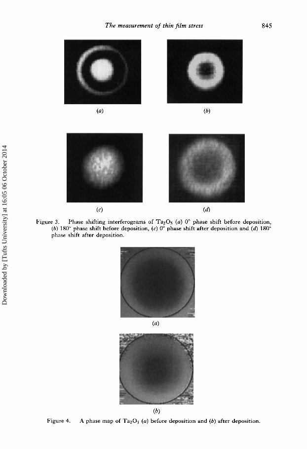
In the present work, we use the PSI technique to develop a PC-based stress measurement system. Film stress is measured by a phase shifting Twyman-Green interferometer (figure 1). The uncoated or coated substrate is mounted vertically at the centre of the sample holder used as the test plate. The sample holder has a circular aperture through which the incident beam passes and is then reflected onto the substrate surface. After two beam reflections, interference fringes of equal thickness arise between the surface of the reference plate and the surface of the substrate. The interference fringes show contours like the shape of the substrate surface. The PSI technique is used to provide fringe patterns with phase shifting. A computer-controlled image frame grabber captures the active images and digitizes them. The computer can also control the programmable dc power supply to provide the voltage to drive the PZT. The PZT stage generates a 79.1 nm displacement and shifts the fringes to a quarter fringe. Five interferograms with constant phase difference (7r/2) between the frames are obtained. We shall choose a Ta2O5 film as an example, to demonstrate the PSI method of film stress determination. Fringe patterns of 0" and a 180" phase shift before Ta2O5 deposi- tion are shown in figures 3 ( a ) and (b ) , and those of 0" and a 180" phase shift after TazOs deposition are shown in figures 3(c) and (4. Since there is a 180" phase
and 0.6 x
Dow
nloa
ded
by [
Tuf
ts U
nive
rsity
] at
16:
05 0
6 O
ctob
er 2
014
The measurement of thin jilm stress 845
Figure 3 . Phase shifting interferograms of Ta205 (a ) 0" phase shift before deposition, ( b ) 180" phase shift before deposition, (c) 0" phase shift after deposition and (d) 180" phase shift after deposition.
( b ) Figure 4. A phase map of T a 2 0 5 (a) before deposition and (b ) after deposition.
Dow
nloa
ded
by [
Tuf
ts U
nive
rsity
] at
16:
05 0
6 O
ctob
er 2
014
846 C.-L. Tien et al.
(4
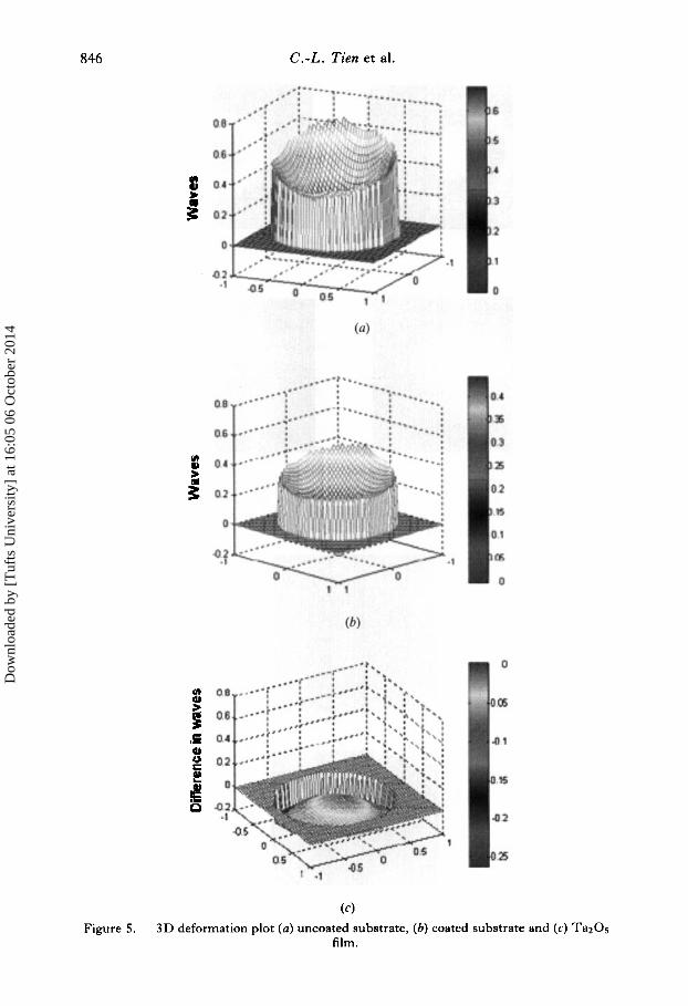
film. Figure 5 . 3D deformation plot (a) uncoated substrate, (b ) coated substrate and (c) Ta205
Dow
nloa
ded
by [
Tuf
ts U
nive
rsity
] at
16:
05 0
6 O
ctob
er 2
014

Tab
le 2
. C
ompa
riso
n of
thi
n fil
m s
tres
s us
ing
diff
eren
t te
chni
ques
2 m :
2 th
ickn
ess
stre
ss
Site
s*
McN
eilb
M
artin
b St
raus
d E
dlin
ger'
5
(GW
(G
Pa)
(G
W
(GP
a)
(GP
a)
(GP
a)
tb 2
Mat
eria
l (P
m)
Si02
0.
270
-0.5
21
-0.7
N -0
.8
-0.6
1 N -1
.6
-0.7
5
Ti0
2 0.
279
-0.4
70
-0.4
-0
.54
%
0.18
9 -0
.489
-0
.4 N
-0
.5
-0.2
N -0
.4
-0.5
5 0
0.27
4 -0
.328
-0
.2 N
-0
.5
$
Thi
n fil
m
Mea
sure
d
Ta2
05
Nb
20S
a Pr
epar
ed b
y io
n be
am s
putt
er d
epos
itio
n.
Prep
ared
by
ion
beam
dep
osit
ion.
Pr
epar
ed b
y re
activ
e lo
w v
olta
ge io
n pl
atin
g.
Dow
nloa
ded
by [
Tuf
ts U
nive
rsity
] at
16:
05 0
6 O
ctob
er 2
014

848 C.-L. Tien et al.
shift between the first and the third frames, they appear nominally out of phase. The program sets a 200 grey-level to present the fringe pattern waves. Phase maps before and after film deposition are shown in figure 4. By using the Zernike polynomial fitting for the wavefront being tested, wavefronts for the uncoated and coated substrates are obtained. Figures 5 (a) and ( b ) show the three-dimensional (3D) contour plot of wavefronts before and after Ta205 deposition, respectively. Subtracting the wavefront in figure 5 (b) from figure 5 (a) , the wavefront difference is obtained, shown in figure 5 ( c ) . From figure S ( c ) , the film deformation is obtained and the average stress is calculated.
The measurement of the stress in Si02, Ti02 and Nb205 follows the same proceedings. The results show that the intrinsic stresses of the four oxide films are compressive. Both the tensile and compressive stresses are observed for a given material, depending upon the deposition conditions and the chemical reactivity of the material. Efforts have been made to explain the mechanisms that induce these stresses. While no one model can explain all the experimental data, the ion peening model proposed by d’Herule [23] successfully explains stresses observed in sputtered films. The intrinsic stresses in the four oxide films are determined by the PSI technique described above, the measured stresses are -0.521 GPa for Si02, -0.470 GPa for TiO2, -0.489 GPa for Ta205 and -0.328 GPa for Nb205. Table 2 summarizes the results for the four oxides’ film stresses measured by the PSI technique. For comparison, the table also lists the literature values for the same films, and from the work of Sites et al. [24], McNeil et al. [25], Martin et al. [26], Strauss et al. [27], and Edlinger et al. [28]. By comparing data for the same type of oxide film, but measured and deposited by different techniques, we find that the results from the PSI method agree well with previous measurements.
4. Conclusion We have developed a novel measurement system for film stress measurement
by using phase shifting interferometry. The PSI technique is well suited to the precise and localized measurement of thin film stress. It has the advantages of inherently high sensitivity, accuracy, easy operation and reproducible perform- ance. In particular the Zernike polynomial fitting algorithm can generate a 3D contour plot of film deformation, indicates tensile stress (downward deflection) or compressive stress (upward deflection). We also show that the measured stress values are in agreement with those of other techniques. Hence, the proposed technique should be useful in measuring stress in thin films.
References [l] THORNTON, J. A. and HOFFMAN, D. W., 1989, Thin Solid Films, 171, 5. [ 2 ] FINEGAN, J. D. and HOFFMAN, R. W., 1959, J . Appl. Phys., 30, 597. [3] ENNOS, A. E., 1966, Appl. Optics, 5 , 51. [4] ROLL, K. and HOFFMANN, H., 1976, Reo. SEE’. Znstrum., 47, 1183. [S] KLOKHOLM, E., 1969, Rev. Sci. Znstrum., 40, 1054. [6] KINOSITA, K., 1972, Thin Solid Films, 12, 17. [7] HOFFMAN, R. W., 1976, Thin Solid Films, 34, 185. [S] SAHU, S. N., SCARMINIO, J. and DECKER, F., 1990, J . Electrochem. SOC., 137, 1150. [9] SADER, D., ENDERS, A. and KIRSCHNER, J., 1995, Rew. Sci. Znstrum., 66, 4734.
Dow
nloa
ded
by [
Tuf
ts U
nive
rsity
] at
16:
05 0
6 O
ctob
er 2
014
The measurement of thin fi lm stress 849
[lo] CAMBELL, D. S., 1970, Handbook of Thin Film Technology, edited by L. I. Massel and
[ l l ] SINHA, A. K., LEVINSTEIN, H. J. and SMITH, T. E., 1978, J. Appl. Phys., 49, 2423. [12] AOKI, T., NISHIKAWA, Y. and KATO, S., 1989, Jpn. J . Appl. Phys., 28, 299. [13] MACK, L. M., REISMAN, A. and BHATTACHARYA, P. K., 1989, J . Electrochem. SOC., 136,
[14] GARDNER, D. S. and FLINN, P. A,, 1990, J. Appl. Phys., 67, 1831. [15] FAHNLINE, D. E., MASTERS, C. B. and SALAMON, N. J., 1991, J . Vac. Sci. Technol., A9,
[16] KOBEDA, E. and IRENE, E. A., 1986, J. Vac. Sci. Technol., B4, 720. [17] ASKRABA, S., CUSSEN, L. D. and SZAJMAN, J., 1996, Meas. Sci. Technol., 7, 939. [18] HARIHARAN, P., OREB, B. F. and EIJU, T., 1987, Appl. Optics, 26, 2504. [19] STONEY, G. G., 1909, Proc. R. SOC. London Ser., A82, 172. [20] DAVIDENKOV, N. N., 1961, Sov. Phys.: Solid State, 2, 2595. [21] KIM, C. J., 1982, Appl. Optics, 21, 4521. [22] MALACARA, D. and DEVORE, S. L., 1992, Optical Shop Testing, edited by D. Malacara
(New York: Wiley), pp. 456-484. [23] D'HERULE, F. M., 1970, Met. Trans., 1, 725. [24] SITES, J. R., GILSTRAP, P. and RUJKORAKARN, R., 1983, Opt. Eng., 22, 447. [25] MCNEIL, J. R., BARRON, A. C., WILSON, S. R. and HERMANN, W. C., 1984, Appl. Optics,
[26] MARTIN, P. J., BENDAVID, A,, SWAIN, M., et al., 1994, Thin Solid Films, 239, 181. [27] STRAWS, G. N., DANH, N. Q. and PULKER, H. K., 1997, J . Non-Cryst. Solids, 218, 256. [28] EDLINGER, J., RAMM, J. and PULKER, H. K., 1989, Thin Solid Films, 175, 207.
R. Glang (New York: McGraw-Hill), pp. 12-30.
3433.
2483.
23, 552.
Dow
nloa
ded
by [
Tuf
ts U
nive
rsity
] at
16:
05 0
6 O
ctob
er 2
014