soc encounter provides smart solution for 90nm … · soc encounter provides smart solution for...
TRANSCRIPT
SoC Encounter Provides Smart Solution for 90nm Dragon-Ball Chip
Wei Sufen
Asia Pacific Region Wireless & Mobile System Group
Freescale Semiconductor
Abstract By employing the solutions provided by Cadence SoC Encounter (SOC.41), the physical integration team at Freescale Suzhou division has developed a smart semi-automatic physical implementation flow. This environment employs the technologies developed in Encounter to address the challenge of physical partition implementation with respect to the key factors of area, timing, power, and signal integrity. This flow has been successfully used to perform physical implementation of a System-On-Chip Dragon-ball product designed in 90nm technology with 7 metal layers involving 5.5 millions of gate-account. The robustness and the capacity of the flow is an asset with regards to the size of physical partitions and the aggressive time-to-market pressure. And it gives designers a very accurate control of runtime against of Quality of Result. This paper discusses the whole flow, which includes from hierarchical floorplan by First Encounter; chip level clock tree generation by Encounter-CTS; signal route by NanoRoute; and post optimization and SI fix by Encounter.
CDNLive! 2005 1 SOC Encounter Provides Smart Solution for 90nm Dragon-Ball Chip

1 Introduction System on Chip (SoC) design development is a challenging activity, especially when geometry scaled down to 90nm and 65nm, the cell accounts are over multi-million gates, the fastest clock frequency is over 400Mhz. The design turn around time, the intermediate data release time-phase, and tape-out are all decided by more factors as: area, timing closure, SI closure, power reduction, and function verification pass. In these years, considerable improvements have been achieved on the methodology development for deep-submicron SoC design to fasten the steps from gate-level netlist to final tape-out GDSII. It covers: actually automatic partitioning; the sound design floor-planning; power-grid analysis; better clock tree insertion; optimized route, post-route timing fix; and SI repair. By a real product, this paper shows what the value and efficiency the flow demonstrates by employing the solutions SoC-Encounter (Cadence-SoC-4.1) provides for whole chip physical integration. 1.1 Introduction of Physical integration flow Working in a multi-design-center context on very large and complex systems-on-chip, a hierarchical top-down approach is a must, leading to multiple physical partitions to deal with as well as the database multiplication. One of our first goals is to standardize and increase productivity of the implementation process, by creating whole standard scripts for all single-pass flow for every partition’s physical designers, as well as for chip physical designers. It covers the standard synthesis scripts, the demo floor-plan scripts, the clock tree scripts, place and route scripts, post optimization scripts and SI repair scripts. Most scripts are TCL based, and aided by PERL in some places. This solution provides a skeleton of code to increase the ease of use and decrease the user’s error factor. On the other hand, criterions are set up for all hard-module’s deliveries for finally building up the whole chip. Fig 1.1 shows the whole physical integration flow for our methodology. It sticks to Encounter environment for whole physical integration except the physical synthesis, which is done by Physical-Compiler. Currently, the evaluation is ongoing in our team for comparison the synthesis QOR between Physical-Compiler and RTL Compiler. Maybe we can discuss and share the result in next presentation. Flow consists of:
— Chip Partition, and the detail chip floorplan. Then performs in parallel the detailed flooplan for every partitioned hard-block. Done by First Encounter.
— Chip level synthesis and Place. Done by Physical Compiler. — Whole physical implementation for every partitions, then deliver timing and physical views
to chip level. — Chip level clock tree generation. Done by Encounter-CTS. — Chip level signal route. Done by Encounter NanoRoute.
CDNLive! 2005 2 SOC Encounter Provides Smart Solution for 90nm Dragon-Ball Chip

— Chip level post optimization and SI repair. Done by Prime-time, Clarinet (Freescale internal tool for SI), and Encounter.
— Post functional ECO route. — Logic Equivalence Check. Done by Comformal LEC. — IR drop analysis for chip level and for hard-blocks. Done by Voltage-Storm. — DRC and LVS. Done by Calibre.
Fig 1: Physical implementation flow chart
Tape-out GDSII
StarRC-XT
Clarinet
PrimeTime
LEC
IR Drop analysis
LEC
Chip partition and floorplan
SOG clock tree generation
SOG signal route
Chip flatten
Timing Opt & SI Repair
Functional ECO
Whole chip timing and SI closure
SOG physical synthesis
Hard-module foorplan
Hard-module physical synthesis
Hard-module Clock-tree synthesis
Hard-module signal route
Hard-module timing and SI closure
CDNLive! 2005 3 SOC Encounter Provides Smart Solution for 90nm Dragon-Ball Chip
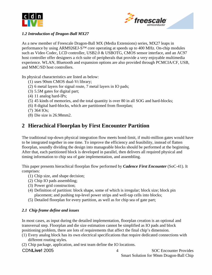
1.2 Introduction of Dragon-Ball MX27 As a new member of Freescale Dragon-Ball MX (Media Extensions) series, MX27 leaps in performance by using ARM926EJ-S™ core operating at speeds up to 400 MHz. On-chip modules such as Video Codec, LCD controller, USB2.0 & USBOTG, CMOS sensor interface, and an AC97 host controller offer designers a rich suite of peripherals that provide a very enjoyable multimedia experience. WLAN, Bluetooth and expansion options are also provided through PCMCIA/CF, USB, and MMC/SD host controllers. Its physical characteristics are listed as below:
(1) uses 90nm CMOS dual-Vt library; (2) 6 metal layers for signal route, 7 metal layers in IO pads; (3) 5.5M gates for digital part; (4) 11 analog hard-IPs; (5) 45 kinds of memories, and the total quantity is over 80 in all SOG and hard-blocks; (6) 8 digital hard-blocks, which are partitioned from floorplan; (7) 364 IOs; (8) Die size is 26.98mm2.
2 Hierachical Floorplan by First Encounter Partition The traditional top-down physical integration flow meets bond-limit, if multi-million gates would have to be integrated together in one time. To improve the efficiency and feasibility, instead of flatten floorplan, soundly dividing the design into manageable blocks should be performed at the beginning. After that, each partitioned block is developed in parallel, then delivers all required physical and timing information to chip sea of gate implementation, and assembling. This paper presents hierachical floorplan flow performed by Cadence First Encounter (SoC-41). It comprises:
(1) Chip size, and shape decision; (2) Chip IO pads assembling; (3) Power grid construction; (4) Definition of partition: block shape, some of which is irregular; block size; block pin
placement; and pushing top-level power strips and well-tap cells into blocks; (5) Detailed floorplan for every partition, as well as for chip sea of gate part;
2.1 Chip frame define and issues In most cases, as input during the detailed implementation, floorplan creation is an optional and transversal step. Floorplan and die size estimation cannot be simplified as IO pads and block positioning problem, there are lots of requirements that affect the final chip’s dimension. (1) Every analog block has its own electrical specifications that require dedicated connections with
different routing styles. (2) Chip package, application, and test team define the IO locations. CDNLive! 2005 4 SOC Encounter Provides
Smart Solution for 90nm Dragon-Ball Chip

(3) Every digital block’s absolute location and relevant placement are decided by IO boundary, and by intra-connection among them. To trim the intra block channel dimensions without wasting silicon area, the pre routing should be created with an acceptable level of accuracy.
(4) After each step, whole trial routing is good estimation to verify design’s route-ability and roughly check congestion map and timing convergence.
At the beginning phase of the project definition step, when the netlist is not stable, IO can be modified, the die size needs to be taken under the value of forecast. On another point of view, the earlier a die size fixed and the optimized floorplan completed, the more helpful to allows a further designer to develop the later implementation. Several iterations are required, so it is very important prepare a suit of easily used scripts. MX27 has 364 IO pads. Its size is 26.98mm with an almost square shape: 5100um * 5290um. 2.2 Power plan and special nets route MX27 has intensive power grids: using comb-structure power strip from m2 to m6 with very narrow steps. This close power net-works are pushed from top-level to partitions. As a result, almost no additional block rings are needed for specific blocks in main functional power domain. However, there is still some critical block (ARM926EJ-S™ platform) that requires dedicated network even if starting from the same pads. Other parts of the system work with a separate power domain at different or same voltage. Also, internal voltage level shifter cells are included, they must be connected under strong specifications about maximum net resistance in order to avoid unbalanced voltage drop.
Figure 2-1 Intensive power grid demo Figure 2-2 Separate power domain First Encounter is user friendly in power plan. It is doing good jobs, no matter in primary chip studying phase by Graphic-User-Interface, or in later floorplan refine-tune by automatic scripting. It can draw proper core rings, core strips, and drop well shaped stack vias. And by using special net route CDNLive! 2005 5 SOC Encounter Provides
Smart Solution for 90nm Dragon-Ball Chip

function, it works smartly in connecting specific pad-power-pin to corresponding core ring, connecting block-ring-pin to strips, and then repairing and refining special nets. Finally, the power distribution for our project is a dedicated structure made with a compound of well-proportioned grids, meshes, ripples and point to point connections using different routing styles. 2.3 Perform partition Generally, partition is done after chip frame is decided, and power plan completed. The original soft modules are converted to fences, then into hard-blocks after partition. MX27 partition flow consists of:
(1) Import the entire design. In the very early design phase, there are only stub netlists instead of detailed compiled netlists for some modules, so they are represented as block-box. Shape and size of black-box need to be adjusted according to cell size estimation.
(2) Layout the floorplan by definition of design frame, IO location, manually pre-place all hard-IPs and modules which will eventually becomes partitions. Pre-place the well-tap cells.
(3) Do whole chip power planning. (4) Run Amoeba Place. (5) Run trail route for prototyping, and also trail route is prerequisite to perform partition pin
placement. (6) Partition the design. In this step, the partitioned modules are converted to blocks, and blocks
pins are placed according chip connection. Moreover chip level power strips and well-taps, which are pre-placed and routed, are push down into partition. It helps to avoid the IR drop and physical DRC issue in later assembling phase. Aside to automatic partitioning pin assignment based on trial route information, the more detailed location specification and adjustment are done by group pin constraints, and set pin placement constraints. Route resources are reserved partially inside partitions for top level connections.
(7) Save the Partition. This action creates one directory for each block, and saves its netlist, floorplan, and budgeted timing constraints to it. For top-level designs, this also creates a directory containing the top-level netlist, floorplan, simple timing model, and physical abstract (LEF file) for each partition block or black-boxes. Subsequent work should be done in these block-level and top-level directories for implementing the block-level and top-level designs, respectively.
In MX27, there are 8 partitioned digital blocks. They are: ARM926EJ-S™ platform; H264 module (a video encoding and decoding IP); eMMA module (a multi-media pre-processing and post-processing IP); SAHARA module (chip encrypting IP); EMI module (the key module for all external memory interface controllers); USB module; RTC-SCC module (it is partitioned for working in a separate power domain. When chip enters sleep mode, the main power domain will be shut down, only RTC_SCC works with osc32k.); CMR_CKGATE module (which is the clock heart of the chip comprised of dividers and clock gating cells). Figure 2-3 shows the primary shapes before implement partition. The modules with pink color are fence property. Figure 2-4 shows the finally shapes after partition. As converting to green, the partitioned module becomes hard blocks. The shape and size of partitions have to be adjusted in later phase to match the chip size change.
CDNLive! 2005 6 SOC Encounter Provides Smart Solution for 90nm Dragon-Ball Chip

Figure 2-3 Primary fences before partition
.
Figure 2-4 Hard-blocks after partition CDNLive! 2005 7 SOC Encounter Provides
Smart Solution for 90nm Dragon-Ball Chip

2.5 detailed floorplan after partition From floorplan point of view, there are still lots of work to do after partition, either for chip SOG part, or for blocks. The main tasks are placement for memories and internal hard-macros; memory power connection. The strips network from top level have to be trimmed carefully for memory placement, and well-tap cell need to be deleted or complemented as well. Amoeba Place and Trial Route need to be run to estimate and verify the rationality. Placement blockages and route blockages need to be pre-placed in specific area for saving the resource in chip place and route. 3 Chip level clock tree synthesis by Encounter-CTS Encounter-CTS is the clock tree generation tool for our project. It analyzes the specified clocks in the design, inserts buffers and inverters to eliminate or reduce the clock skew. Meanwhile, clock nets are routed in clock tree building process, and clock tree ECO (by ckECO command) is done after clock nets routed to minish the clock skew. Figure 4-1 is the simplified clock structure diagram for MX27.
scan clock
scan clock
clock gate
clock gate
clock gate
clock gate
clock gate
mpll clock root
1b divider
3b divider
4b divider
6b flp divider
5b divider
3b divider clock gate
clock gate
clock gate
clock gate
clock gate
UPLL
MPLL
from osc32k
CRM-CKGATE
clock gate
clock gate
upll clock root
Figure 4-1: chip clock structure CDNLive! 2005 8 SOC Encounter Provides
Smart Solution for 90nm Dragon-Ball Chip

MX27 constrains two digital-plls inside. One is called upll which is the clock source for 60M Hz frequency USB module. The other one is mpll, which provides the clock source for all modules except USB. Odd number divider, even number divider, and decimal fraction divider are used after the mpll to generate diverse clock frequencies for 400M Hz ARM926EJ-S™ platform, 133M Hz AHB-bus, 66.5M Hz IP-bus, and different baud clocks. To save power, latch-based clock gating cells are instantiated after dividers. So clock will be turned off directly after the divider when the corresponding module enable signal is disabled. All clock dividers and gating cells are grouped together and form CRM_CKGATE module. CRM_CKGATE is also partitioned as hard-block in order to get the best optimized clock source structure and timing from the beginning. External-timing-model (.lib) of CRM_CKGATE is used in CTS. The mpll clock domain is the main and biggest domain for clock tree synthesis. Clock root for main mpll clock domain is set at the output clock of mpll, before the dividers. Encounter-CTS has to trace through two levels latch-based clock gating cells to reach every clock sync pin. The first level clock gating is inside CRM_CKGATE, the second level clock gating cells are inserted by Power-Compiler in synthesis step and disperse over sea of gate. There are 55810 sync pins for mpll clock domains, and contains rising edge clocks, inverted rising edge clock, and falling edge clocks. The input clock pins for every hard-block are also treated as sync pins for top-level clock tree building. Their clock insertion delay value and pin capacitance are presented by MacroModel definition statements. The target clock skew value for mpll clock is less than 300ps, the max insertion delay is less than 5000ps. Clock constraints for building mpll tree are listed in Appendix A. Clock tree post-optimization is done right after the primary tree building, and clock trees are routed inside CTS to get better correlated clock RC delay. By defaults, clock nets are routed in middle metal layers: M3 and M4, and double space rule (extra space 1) is chosen to avoid SI affect on clock nets. Also to achieve smaller trigger edge skew, Encounter-CTS is capable to size the combinational cells and gating cells on clock paths, even flip-flops can be moved a little bit space. Of course, all these default optimization behaviors can be override by setCTSMode command. After the whole clock tree generation procedure completed, Encounter-CTS can also perform ckECO function in post-clock tree stage, in clock route stage, or in all nets routed stage. MX27 chooses to do ckECO right after clock tree routed. ckECO accepts spef file as clock RC input from the external 3-part tool (for example StarRC-XT). Table 4-1 compares the clock result in Encounter after clock synthesis (ckSynthesis) and clock ECO (ckECO). From the reports, a conclusion can be draw that trig-edge skew is the first priority target in clock optimization and ckECO function, and finally CTS really gets it! Asides from calculating RC based on the technology lef file, Encounter also read in the refined 3D extended-capacitance-table. Resistance, default Cap, detailed Cap, and crossed Cap values can be adjusted manually. It is based on the detailed RC, which is extracted from Encounter after clock nets routed or all signal nets routed, compares to the extracted RC from the RC sign-off tool. This comparison can be done by Ostrich inside Encounter. Figure 4-2 shows the detailed capacitance comparison statistic curve between Encounter and StarRC-XT, the calculated value is 1.02. As the extended-cap-table is used, after Ostrich correlation, the default cap, detailed cap, x-cap, and resistance value are all set to default 1 to get a best clock tree result. CDNLive! 2005 9 SOC Encounter Provides
Smart Solution for 90nm Dragon-Ball Chip
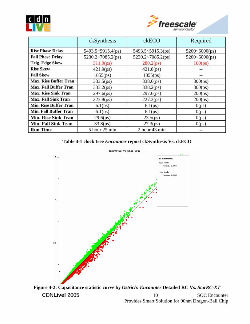
ckSynthesis ckECO Required
Rise Phase Delay 5493.5~5915.4(ps) 5493.5~5915.3(ps) 5200~6000(ps) Fall Phase Delay 5230.2~7085.2(ps) 5230.2~7085.2(ps) 5200~6000(ps) Trig. Edge Skew 311.9(ps) 280.2(ps) 100(ps) Rise Skew 421.9(ps) 421.8(ps) -- Fall Skew 1855(ps) 1855(ps) -- Max. Rise Buffer Tran 333.5(ps) 338.6(ps) 300(ps) Max. Fall Buffer Tran 333.2(ps) 338.2(ps) 300(ps) Max. Rise Sink Tran 297.6(ps) 297.6(ps) 200(ps) Max. Fall Sink Tran 223.8(ps) 227.3(ps) 200(ps) Min. Rise Buffer Tran 6.1(ps) 6.1(ps) 0(ps) Min. Fall Buffer Tran 6.1(ps) 6.1(ps) 0(ps) Min. Rise Sink Tran 29.6(ps) 23.5(ps) 0(ps) Min. Fall Sink Tran 33.8(ps) 27.3(ps) 0(ps) Run Time 5 hour 25 min 2 hour 43 min --
Table 4-1 clock tree Encounter report ckSynthesis Vs. ckECO
Figure 4-2: Capacitance statistic curve by Ostrich: Encounter Detailed RC Vs. StarRC-XT
CDNLive! 2005 10 SOC Encounter Provides Smart Solution for 90nm Dragon-Ball Chip

4 Chip level route by NanoRoute In MX27, all blocks and top level sea of gate parts use Encounter NanoRoute as signal route tool. NanRoute has below features to take ascendant on deep-submicron SOC route:
(1) It performs concurrent signal integrity, timing-driven, and manufacturing aware routing, which are called S.M.A.R.T routing technology. (2) Support 180 nm, 130 nm, and 90 nm process. (3) Can handle more than 300K instances or nets and at least five routing layers. There are 6 metal route layers in MX27, with 350K instances in chip SOG part, and 350K instance in one bigger hard-block, H264 module. (4) To improve the run efficiency, it performs distributed routing on multiple workstations running multi-threading (super threading). (5) Complex wide wire spacing rule support, density checking and fill, minimum area and notch (donut) avoidance (6) Via stacking, diagonal spacing, and density rule support (7) LEF file optimization (8) Automatic track generation (9) Manufacturing-aware routing support, including wire spreading and support for redundant vias (10) Open timing architecture, including support for Encounter common timing engine (CTE) and external timing engines such as PrimeTime. (11) Support for third-party data files, including customized LEF technology files and Astro files, and older-syntax LEF files.
Our project has three route phases:
(1) The first phase is the first global and detail route after clock tree complete. Of course, the design should be fully placed, and all special nets should be routed correctly. The command “checkPlace” is recommended to use in any phase in Encounter to check the placement statue: are there any over-lapped cells, or any un-placed cells? And “checkUnique” checks whether design is properly uniquified after synthesis. During the global route step, NanoRoute breaks the design into rectangles called global routing cells (gcells). It finds connections for the regular nets defined in the NETS section of the DEF file by assigning them to the gcells. The goals of global routing are to distribute and minimize congestion and to minimize the number of gcells that have more nets assigned than routing resources available. Then, it updates the congestion map. In the detail route step, Nanoroute follows the global routing plan and lays down actual wires that connect the pins to their corresponding nets. The detailed router is less conservative than the global router—it creates shorts or spacing violations rather than leave unconnected nets. Then it keeps running search-and-repair routing technology during detailed routing. During search and repair, it locates shorts and spacing violations and reroutes the areas to eliminate as many violations and shorts as possible. The primary goal of detailed routing is to complete all of the required interconnect without leaving shorts or spacing violations.
CDNLive! 2005 11 SOC Encounter Provides Smart Solution for 90nm Dragon-Ball Chip

The command “setNanoRouteMode” controls route mode. Such as: if using timing-driven route; if using SI-driven route; if fixing antenna violations during route. And “setAttribute” command set specific characters on selected nets during route. For example, it is widely used to keep double-space route attribute on all clock nets and SI victim nets, and to avoid detour routing for them. Appendix B shows the demo setting for globalDetailRoute.
(2) The second phase is functional ECO route. ECO route is often chosen when any ECO place is done under post-route phase. Both global and detailed route are run in ECO route, NanoRoute makes as minimal changes as possible to the topology of fully routed nets.
(3) The third phase is another round of ECO route to make the physical design rule clean. Since
the first round of global and detail route may leave some short and space violations, the violations nets can be deleted by command “editDeleteViolations”, then reroute these nets by ECO route. Antenna violation can also be fixed by jog metal layers, by inserting antenna diode, or by sizing up the receiver cell to containing bigger gate area. Density violation can be fixed in NanoRoute too. In our library, there are special decap filler cell and OD filler cell to be inserted to alleviate metal and AP layer density violations.
The Table 5-1 shows the run time, and DRC result for NanoRoute in first globalDetailRoute, and two more rounds of ECO route to fix DRC. In the first 2 route, clock nets are kept the fixed property, in the third route, they are changed to place attribute. The reason is that there is a library issue for one size of clock gating cell in clock path. Its pin in metal 1 protrudes a little branch exposing to 90 degree direction, which is easily shorted with other signal nets. About 35 percent of DRC violations come from such short error. To solve this problem, clock nets are trying to keep be fixed in the primary globalDetailRoute and the succedent ECO Route, then change to route attribute in the later route of ECO route, it is a trade-off tactic for keeping clock integrality and solving DRC error.
First globalDetailroute
ECO Route Run1
ECO Route Run2
DRC Error Left 2350 470 55
Run Time 12 hour 35min 5 hour 3 hour 30 min
Table 5-1 DRC Error and Runtime Comparison Tabel
5 Post-Opt and SI fix by Encounter Post optimization always need be done to achieve timing and SI closure. There are two targets in our projects: (1) Setup timing clean before taking account of SI induced timing violations; (2) Fix SI timing violation, which includes setup and hold fix, and SI functional noise repair.
CDNLive! 2005 12 SOC Encounter Provides Smart Solution for 90nm Dragon-Ball Chip
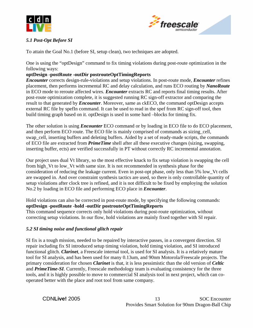
5.1 Post-Opt Before SI To attain the Goal No.1 (before SI, setup clean), two techniques are adopted. One is using the “optDesign” command to fix timing violations during post-route optimization in the following ways: optDesign -postRoute -outDir postrouteOptTimingReports Encounter corrects design-rule-violations and setup violations. In post-route mode, Encounter refines placement, then performs incremental RC and delay calculation, and runs ECO routing by NanoRoute in ECO mode to reroute affected wires. Encounter extracts RC and reports final timing results. After post-route optimization complete, it is suggested running RC sign-off extractor and comparing the result to that generated by Encounter. Moreover, same as ckECO, the command optDesign accepts external RC file by spefIn command. It can be used to read in the spef from RC sign-off tool, then build timing graph based on it. optDesign is used in some hard –blocks for timing fix. The other solution is using Encounter ECO command or by loading in ECO file to do ECO placement, and then perform ECO route. The ECO file is mainly comprised of commands as sizing_cell, swap_cell, inserting buffers and deleting buffers. Aided by a set of ready-made scripts, the commands of ECO file are extracted from PrimeTime shell after all these executive changes (sizing, swapping, inserting buffer, ects) are verified successfully in PT without correctly RC incremental annotation. Our project uses dual Vt library, so the most effective knack to fix setup violation is swapping the cell from high_Vt to low_Vt with same size. It is not recommended in synthesis phase for the consideration of reducing the leakage current. Even in post-opt phase, only less than 5% low_Vt cells are swapped in. And over constraint synthesis tactics are used, so there is only controllable quantity of setup violations after clock tree is refined, and it is not difficult to be fixed by employing the solution No.2 by loading in ECO file and performing ECO place in Encounter. Hold violations can also be corrected in post-route mode, by specifying the following commands: optDesign -postRoute -hold -outDir postrouteOptTimingReports This command sequence corrects only hold violations during post-route optimization, without correcting setup violations. In our flow, hold violations are mainly fixed together with SI repair. 5.2 SI timing noise and functional glitch repair SI fix is a tough mission, needed to be repaired by interactive passes, in a convergent direction. SI repair including fix SI introduced setup timing violation, hold timing violation, and SI introduced functional glitch. Clarinet, a Freescale internal tool, is used for SI analysis. It is a relatively mature tool for SI analysis, and has been used for many 0.13um, and 90nm Motorola/Freescale projects. The primary consideration for chosen Clarinet is that, it is less pessimistic than the old version of Celtic and PrimeTime-SI. Currently, Freescale methodology team is evaluating consistency for the three tools, and it is highly possible to move to commercial SI analysis tool in next project, which can co-operated better with the place and root tool from same company.
CDNLive! 2005 13 SOC Encounter Provides Smart Solution for 90nm Dragon-Ball Chip

SI analysis and repair is a complex flow, so in our project, we build a whole automatic environment to integrate StarRC-XT, Clarinet, PrimeTime, and Encounter together. SI functional failed nets are extracted from Clarinet by two rounds of iterations to reduce conservative. SI repair solutions are mainly comprised of:
(1) double-space nets; (2) sizing driven cells; (3) insert buffer in victim nets.
The repair directives are verified in Clarinet, and then feed to Encounter. SI delay analysis combines Clarinet and Primetime together. The SI introduced delta delays are calculated by two iterations in Clarinet, and then annotated back to Primetime. Scripts are used in PT shell to sizing_cell, swap_cell, re-route nets, insert-buffers to fix setup, hold, and transition violation. And all the commands are summarized and merged with functional directives for Encounter in one fix. Figure6-1 shows the SI analysis and repair flow for setup timing; Figure6-2 shows the flow for hold timing; Figure6-3 shows the flow for function noise
Figure 6-1 SI setup delay analysis and repair flow
CDNLive! 2005 14 SOC Encounter Provides Smart Solution for 90nm Dragon-Ball Chip

Figure 6-2 SI hold delay analysis and repair flow
Fig 6-3 SI function analysis/repair flow
CDNLive! 2005 15 SOC Encounter Provides Smart Solution for 90nm Dragon-Ball Chip

6 Conclusion Through the links of scripts, in a semi-automatic flow, Encounter helps us to tape-out a very critical and challenging 90nm new dragon-ball design for a hand-set application. Nevertheless, in a close partnership with Cadence SOC Encounter, we are keeping working to improve the solution. Here we present the issues, and suggestions for both methodology and tool enhancement.
(1) In Encounter linux version, Sroute in floorplan may crash. So we have to stick to solaris binary for Sroute.
(2) In clock tree synthesis step, Encounter-CTS can balance trigger edge skew. However, in our
project, in some hard block, from the same clock input pin, the clock tree connects to both rising edge triggered flip-flops, and falling edge flip-flops, and there is timing check between them. In chip-level clock tree building phase, Encounter-CTS can not balance the rising edge skew of this hard block’s clock pin to falling edge skew of itself. So it has to be done by manually ECO to adjust the clock buffer/inverter to get symmetrical rising and falling clock delay.
(3) As timing sign-off by Primetime, there is a timing co-relation issue between Encounter timing
engine and PT timing engine. It must be careful to use the command optDesign in Encounter : we should adjust RC in Encounter to get consistent timing result with Primetime before we perform timing optimization automatically in Encounter. Else, we may over-action, or perform an un-sufficient repair.
(4) We need to further improve our methodology in tools link-up, in order to get a robust,
predictable, and convergent flow, able to resolve our time-to-market constraints in a push-button way.
7 Reference [1] “Encounter User Guide”, Product Version 4.1, June 2004 [2] “Encounter Test Command Reference” Product Version 4.1, June 2004 [3] “Encounter Timing Closure Guide”, Product Version 4.1, June 2004 [4] “Encounter Database Access Command Reference”, Product Version 4.1, June 2004
8 Appendix 8.1 Appendix A: mpll clock tree synthesis demo constraint for Encounter-CTS ############################### # Routing section # ############################### RouteTypeName FE_CTS_USER1 NonDefaultRule double_space TopPreferredLayer 4 BottomPreferredLayer 3
CDNLive! 2005 16 SOC Encounter Provides Smart Solution for 90nm Dragon-Ball Chip

End ################################ # CLOCKS from crm_mux_mpll_clk # ################################ AutoCTSRootPin bono_coremux/bono_core/crm/crm_synth/crm_clkc_ip/U_mux_mpll_buf2/x MaxDelay 6000ps MinDelay 5200ps SinkMaxTran 200ps BufMaxTran 300ps MaxSkew 100ps MaxFanout 30 NoGating NO RouteType FE_CTS_USER1 LeafRouteType default RouteClkNet YES Obstruction YES DetailReport YES PostOpt YES OptAddBuffer YES OptAddBufferLimit 20 Buffer buf_s_hivt_8 buf_s_hivt_16 buf_s_hivt_24 inv_s_hivt_8 inv_s_hivt_16 inv_s_hivt_24 LeafPin #clk_always_a926p + bono_coremux/bono_core/a926p/clk_always rising + bono_coremux/bono_core/a926p/ipt_clk_wrapper[0] rising …… ThroughPin + bono_coremux/bono_core/crm/crm_synth/crm_clkc_ip/crm_ckgate/crm_mux_mpll_clk ExcludedPin #hclken_a926p + bono_coremux/bono_core/a926p/hclken …… …… End 8.2 Appendix B: NanoRoute globalDetaiRoute command demo
setAttribute -net @CLOCK -non_default_rule double_space -avoid_detour true setNanoRouteMode -quiet drouteFixAntenna true setNanoRouteMode -quiet routeInsertAntennaDiode false setNanoRouteMode -quiet routeAntennaCellName default setNanoRouteMode -quiet routeWithTimingDriven true setNanoRouteMode -quiet routeWithTimingOpt false setNanoRouteMode -quiet optimizeBi false setNanoRouteMode -quiet optimizeGs false setNanoRouteMode -quiet optimizeFixSetupTime false setNanoRouteMode -quiet optimizeTargetSetupSlack 0.000000
CDNLive! 2005 17 SOC Encounter Provides Smart Solution for 90nm Dragon-Ball Chip

setNanoRouteMode -quiet optimizeFixHoldTime false setNanoRouteMode -quiet optimizeTargetHoldSlack 0.000000 setNanoRouteMode -quiet routeWithSiDriven true setNanoRouteMode -quiet routeSiEffort high setNanoRouteMode -quiet routeWithSiPostRouteFix false setNanoRouteMode -quiet drouteAutoStop false setNanoRouteMode -quiet drouteStartIteration default setNanoRouteMode -quiet routeTopRoutingLayer 6 setNanoRouteMode -quiet envNumberProcessor 10 setNanoRouteMode -quiet drouteEndIteration default setNanoRouteMode -quiet routeSelectedNetOnly false setNanoRouteMode -quiet grouteMinimizeCongestion true setNanoRouteMode -quiet drouteHonorMinFeature true setNanoRouteMode -quiet routeAutoGgrid true setNanoRouteMode -quiet routeWithEco false getNanoRouteMode -quiet routeSiEffort getNanoRouteMode -quiet globalDetailRoute
9 Acknowledgements Here presents the earnest appreciation to our physical design team and CAD member for developing the flow, contributing to born this paper out. The paper consecrates to our product: MX27, whose nick name is Bono. Hope she first-silicon pass successful. Wei Sufen (Stella Wei) Senior Digital IC design engineer with Wireless & Mobile Sector, Freescale Semiconductor, SuZhou Design Center; Has being working with Motorola-Freescale for more than 5 years, in the field of DFT and physical integration; Has extensive experience with logical synthesis, physical synthesis, floorplan, place & route, clock tree synthesis, Static timing analysis (STA), signal integrity(SI) analysis/fix, post layout optimization, and DRC/LVS for both hard macro and entire chip level tapeout; Winner of the “Best Paper” prize for 2003 Synopsys SNUG in China; Obtained MSEE in 2001 and BSEE in 1998, both from XianJiaoTong University, China.
CDNLive! 2005 18 SOC Encounter Provides Smart Solution for 90nm Dragon-Ball Chip